EP1796373A1 - Imaging method with an image sensor with a high dynamic range - Google Patents
Imaging method with an image sensor with a high dynamic rangeDownload PDFInfo
- Publication number
- EP1796373A1 EP1796373A1EP05111984AEP05111984AEP1796373A1EP 1796373 A1EP1796373 A1EP 1796373A1EP 05111984 AEP05111984 AEP 05111984AEP 05111984 AEP05111984 AEP 05111984AEP 1796373 A1EP1796373 A1EP 1796373A1
- Authority
- EP
- European Patent Office
- Prior art keywords
- transistor
- voltage
- photodiode
- initialization
- terminal
- Prior art date
- Legal status (The legal status is an assumption and is not a legal conclusion. Google has not performed a legal analysis and makes no representation as to the accuracy of the status listed.)
- Withdrawn
Links
- 238000003384imaging methodMethods0.000titledescription4
- 239000003990capacitorSubstances0.000claimsabstractdescription54
- 238000000034methodMethods0.000claimsabstractdescription41
- 238000005286illuminationMethods0.000claimsabstractdescription26
- 238000005070samplingMethods0.000claimsabstractdescription18
- 239000002800charge carrierSubstances0.000claimsabstractdescription8
- 238000005516engineering processMethods0.000claimsdescription5
- FGUUSXIOTUKUDN-IBGZPJMESA-NC1(=CC=CC=C1)N1C2=C(NC([C@H](C1)NC=1OC(=NN=1)C1=CC=CC=C1)=O)C=CC=C2Chemical compoundC1(=CC=CC=C1)N1C2=C(NC([C@H](C1)NC=1OC(=NN=1)C1=CC=CC=C1)=O)C=CC=C2FGUUSXIOTUKUDN-IBGZPJMESA-N0.000claims1
- 238000005259measurementMethods0.000claims1
- 238000010586diagramMethods0.000description7
- 239000011159matrix materialSubstances0.000description6
- 230000010354integrationEffects0.000description4
- 230000006870functionEffects0.000description3
- 238000009792diffusion processMethods0.000description2
- 230000000694effectsEffects0.000description2
- 238000004519manufacturing processMethods0.000description2
- 101150018075sel-2 geneProteins0.000description2
- 239000004065semiconductorSubstances0.000description2
- 239000000758substrateSubstances0.000description2
- 230000001419dependent effectEffects0.000description1
- 238000002955isolationMethods0.000description1
- 230000010287polarizationEffects0.000description1
- 229920006395saturated elastomerPolymers0.000description1
- 230000002123temporal effectEffects0.000description1
Images

Classifications
- H—ELECTRICITY
- H04—ELECTRIC COMMUNICATION TECHNIQUE
- H04N—PICTORIAL COMMUNICATION, e.g. TELEVISION
- H04N25/00—Circuitry of solid-state image sensors [SSIS]; Control thereof
- H04N25/50—Control of the SSIS exposure
- H04N25/57—Control of the dynamic range
- H04N25/571—Control of the dynamic range involving a non-linear response
- H04N25/575—Control of the dynamic range involving a non-linear response with a response composed of multiple slopes
- H—ELECTRICITY
- H04—ELECTRIC COMMUNICATION TECHNIQUE
- H04N—PICTORIAL COMMUNICATION, e.g. TELEVISION
- H04N25/00—Circuitry of solid-state image sensors [SSIS]; Control thereof
- H04N25/50—Control of the SSIS exposure
- H04N25/57—Control of the dynamic range
- H—ELECTRICITY
- H04—ELECTRIC COMMUNICATION TECHNIQUE
- H04N—PICTORIAL COMMUNICATION, e.g. TELEVISION
- H04N25/00—Circuitry of solid-state image sensors [SSIS]; Control thereof
- H04N25/50—Control of the SSIS exposure
- H04N25/57—Control of the dynamic range
- H04N25/58—Control of the dynamic range involving two or more exposures
- H—ELECTRICITY
- H04—ELECTRIC COMMUNICATION TECHNIQUE
- H04N—PICTORIAL COMMUNICATION, e.g. TELEVISION
- H04N25/00—Circuitry of solid-state image sensors [SSIS]; Control thereof
- H04N25/50—Control of the SSIS exposure
- H04N25/57—Control of the dynamic range
- H04N25/59—Control of the dynamic range by controlling the amount of charge storable in the pixel, e.g. modification of the charge conversion ratio of the floating node capacitance
- H—ELECTRICITY
- H04—ELECTRIC COMMUNICATION TECHNIQUE
- H04N—PICTORIAL COMMUNICATION, e.g. TELEVISION
- H04N25/00—Circuitry of solid-state image sensors [SSIS]; Control thereof
- H04N25/70—SSIS architectures; Circuits associated therewith
- H04N25/76—Addressed sensors, e.g. MOS or CMOS sensors
- H—ELECTRICITY
- H04—ELECTRIC COMMUNICATION TECHNIQUE
- H04N—PICTORIAL COMMUNICATION, e.g. TELEVISION
- H04N25/00—Circuitry of solid-state image sensors [SSIS]; Control thereof
- H04N25/70—SSIS architectures; Circuits associated therewith
- H04N25/76—Addressed sensors, e.g. MOS or CMOS sensors
- H04N25/77—Pixel circuitry, e.g. memories, A/D converters, pixel amplifiers, shared circuits or shared components
Definitions
- the inventionrelates to a method for obtaining an image using an extended dynamic range image sensor.
- the image sensorcan be easily made for example in a technology of the CMOS type.
- CMOS image sensorsare intended for example for the production of photographic devices that can equip small portable instruments, such as wristwatches. In such instruments powered by a battery or accumulator, it is necessary to reduce the power consumption of each electronic component. As a result, the image sensor must be designed in such a way as to consume little electrical energy during imaging or processing operations.
- such an image sensorcomprises, on the same chip, a photosensitive cell formed of a set of pixels, and a processing component intended to perform the imaging and reading operations.
- information captured by the photosensitive cellPixels are typically organized as a matrix arranged in rows and columns. The matrix occupies most of the surface of the sensor.
- an addressing of the corresponding line and columnis carried out.
- the sensortraditionally comprises a line addressing circuit coupled to the lines of the matrix and an output bus coupled to the columns of the matrix, both controlled by a control circuit.
- Photo-detecting elements of the pixels of the cellmay consist of p-n junction capabilities of a semiconductor substrate for capturing photons. These junction capabilities are commonly referred to as photodiodes, which have the advantage of being compatible with standard CMOS manufacturing processes.
- each photodiodeIn normal operation, each photodiode is inversely polarized at a given voltage for example between 0 and 2 V.
- the photons picked up by the photodiodedischarge a capacitance of the photodiode by generating electron-hole pairs. These electron-hole pairs are collected by the opposite electrodes of the capacitance and therefore reduce the voltage deviation across the capacitance in a given dynamic range of sensor voltage.
- This dynamic range of voltage of the sensoris lower than the polarization voltage of the photodiode, for example equal to 1.5 V, but this condition is however not limiting.
- Each pixel of the matrixmay have a structure according to the illustration of Figure 1 equivalent to the structure of Figure 2B of the document EP 1 128 661 of same Applicant, whose description relating to this FIG. 2B and the method of obtaining an image is incorporated herein by reference.
- This pixel 1comprises a photodetector element, such as an inversely polarized photodiode PD, a storage means, such as a capacitor C1 and five transistors M1 to M5, for example of the n-MOS type.
- the photodiodemakes it possible to collect the photo-generated electrons during a so-called integration or exposure period, whereas the storage means makes it possible to memorize the voltage value present at the terminals of the photodiode PD during a sampling phase.
- the transistor M1is connected in series with the photodiode between a high power supply terminal V DD and a low power supply terminal V SS of a not shown voltage source. According to the prior art, this transistor M1, which is controlled by an initialization signal TI on its gate terminal, ensures the initialization of the photodiode PD at a determined voltage before each integration or exposure period.
- the transistor M2connects the capacitor C1 to the connection node between the transistor M1 and the photodiode PD.
- This transistor M2which is controlled by a sampling signal SH, samples the charge accumulated by the photodiode PD and the storage of the signal thus sampled on the capacitor.
- This transistor M2also ensures isolation or decoupling of the photodiode PD and the capacitor C1.
- the transistor M3is connected in series with the capacitor C1 between the two power supply terminals V DD and V SS . According to the prior art, this transistor M3, which is controlled by an initialization signal RST, notably ensures the initialization of the capacitor at a determined voltage.
- the transistor M4is a transistor "source follower transistor” whose gate terminal is connected to the connection node between the source terminal of the transistor M3 and the capacitor C1, and the drain terminal is connected to the high power supply terminal V DD .
- the transistor M4is arranged in series with the transistor M5, which is a line selection transistor.
- the transistor M5, which is controlled by a line selection signal RSEL,ensures, during the reading process, the transfer of the voltage of the transistor M4 to an output bus common to all the pixels in a column.
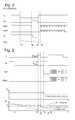
- FIG. 2With reference to FIG. 2, the traditional method of obtaining an image using an image sensor, the structure of each pixel of which is shown in FIG. 1, is described. a temporal diagram of the evolution of the control signals TI, SH, RST and RSEL making it possible to operate the pixel structure of FIG. 1, as well as schematically the evolution of the voltage V PD of the photodiode PD and the evolution of the voltage V 1 on the capacitor C1.
- the first and second initialization signals TI and RSTare both brought to a high positive voltage level close to V DD .
- an initialization respectively of the photodiode PD and the capacitor C1 of each pixelis performed at a determined initialization voltage.
- the sampling signal SHis itself at a low level such that the transistor M2 is not conducting, which makes it possible to decouple the photodiode PD and the capacitor C1.
- the line selection signal RSELis at a low level so that the line selection transistor M5 is not conducting.
- the resulting voltages V PD and V 1 on the photodiode PD and the capacitor C1are therefore at levels substantially equal to the determined initialization voltage.
- the first initialization signal TIgoes to a low level making the transistor M1 non-conductive, which starts the period of exposure or integration of the photodiodes PD of the sensor. images.
- the PD photodiodesbegin to discharge in proportion to the amount of light that each of them receives as shown by the evolution of the voltage V PD between t1 and t3.
- the initialization signal RSTis kept high to maintain the capacitor C1 at a constant voltage level close to V DD .
- the second initialization signal RSTgoes to a low level, thus releasing the memory node on capacitor C1.
- the sampling signal SHthen briefly goes to a high level making the transistor M2 conductive. This allows the sampling of the voltage value present on the photodiode PD and its storage on the capacitor C1.
- the voltage V 1 across the capacitor C1changes as shown in Figure 2.
- the exposure time of the sensorends.
- the capacitor of each pixelkeeps in memory the voltage value of the photodiode as a function of its illumination as soon as the transistor M2 is made non-conductive.
- the first initialization signal TIis brought back to a level such that each photodiode is again initialized at a voltage substantially equal to the initialization voltage close to V DD .
- the sampled voltage stored on the capacitor of each pixel of the sensoris thus not disturbed by the charge carrier diffusion phenomenon, so that the voltage present on this capacitor remains constant.
- a Reading phase of the stored voltage value on the capacitoroccurs at time t4 for each row of pixels of the sensor successively.
- the capacitance of the photodiodeis rapidly discharged to a minimum value of voltage depending on the dynamic range of voltage of the sensor, which is not illustrated in FIG. in case of low or medium illumination of the photodiode, the voltage across the capacitance of the photodiode makes it possible to give a significant information of the captured image.
- the sensorIn order to obtain at the end of a defined exposure period a significant information of the image captured in strong and low illumination, the sensor must include means for increasing its dynamic range of voltage.
- One of the methodsconsists, for example, of fusing two images taken at different exposure times with digital processing. As this requires storing an image in memory, a lot of room on the circuit is used. This is therefore not applicable to an image sensor capable of equipping a small volume instrument. It is also possible to add several electronic components in the pixels of the photosensitive cell of the image sensor to increase the dynamic range. However, in this case, this considerably reduces the light collector area ratio on the pixel surface, which is a disadvantage.
- a second initialization or reset operation of the photodiodeis performed by the MOS transistor at a level below the first initialization voltage.
- this second initialization operationhas no influence on the voltage level of the photodiode.
- the voltage level of the photodiodeis reset to a second initialization voltage lower than the first initialization voltage. The MOS transistor is then disconnected again to begin a second short period of exposure of the photodiode.
- a reading operation of the charge accumulated on the capacitoris performed by means of a mounting of follower transistors. Thanks to at least two exposure periods of the photodiode, it is thus possible to obtain significant information for a weakly, moderately or strongly illuminated photodiode, which has the effect of extending the dynamic range of the sensor voltage. images.
- a disadvantage of the solution proposed in the document WO 2004/064386is that the charge storage capacitor is directly connected to the photodiode. Therefore, at each initialization operation of the photodiode, the capacitor is also initialized at the voltage level of the photodiode. Several operations for reading the value of the voltage on the capacitor must therefore be performed, which complicates the processing of the information provided by each pixel.
- the main purpose of the inventionis thus to provide a method of obtaining an image using an extended dynamic range image sensor by simple means in order to obtain a well-contrasted image at any level of image. illumination by overcoming the disadvantages of the prior art mentioned above.
- the method of obtaining an imagemakes it possible to operate the image sensor by reducing as much as possible its power consumption so as to equip a small volume instrument, such as a watch.
- the inventionrelates to a method for obtaining an image using an extended dynamic range image sensor cited above, which comprises the features mentioned in claim 1.
- An advantage of the method of obtaining an imagelies in the fact that the two initialization operations of the photo-detector element are carried out by the control of two different transistors.
- the second initialization operation of the photo-detector elementis carried out in particular by controlling only the first initialization transistor by a well-defined control voltage applied to its control terminal. This makes it possible to provide a second initialization voltage to the photo-detector element, such as an inversely polarized photodiode, which is lower than the first initialization voltage.
- the second initialization voltagecan be determined by selecting one of a plurality of voltage levels of a control circuit that provides the control signal to the control terminal of the first transistor.
- the different voltage levels of the control circuitare obtained by means of a resistive divider, which preferably comprises more than two resistors connected in series between the two power supply terminals of a DC voltage source of each pixel. .
- the choice of a voltage levelis obtained by controlling a switching transistor connecting a connection node of two adjacent resistors and the control terminal of the first transistor.
- the second exposure period of each photo-detector elementsuch as a photodiode
- the duration of the second exposure periodis 20 times less than the duration of the first exposure period, which makes it possible to speak of an extended dynamic range image sensor.
- the method of obtaining an image using an extended dynamic range image sensorwill be described preferably below on the basis of a pixel structure as shown in FIG. 1 described above.
- the five transistors M1 to M5are preferably n-MOS transistors made in a CMOS technology.
- the drain terminal of the first initialization transistor M1is connected to the high power supply terminal V DD of a DC voltage source not shown.
- the source terminal of the transistor M1is connected to a photo-detector element, which is an inversely polarized PD photodiode connected to the low supply terminal V S of the voltage source.
- the conduction of the transistor M1is controlled by a control signal TI applied to its gate terminal.
- the high voltage level of the control signal TIcan be adapted as explained below with reference to FIG. 4 as a function of the general illumination level of an image pickup by the photosensitive cell of the sensor.
- the drain terminal of the second sampling transistor M2is connected to the connection node of the first transistor M1 and the photodiode PD, whereas the source terminal of the second transistor M2 is connected to a terminal of a capacitor C1, acting as storage medium.
- the conduction of this second transistor M2is controlled by a sampling signal SH applied to its gate terminal.
- Capacitor C1may consist only of p-n junctions across the semiconductor substrate at the memory node.
- the drain terminal of the third initialization transistor M3is connected to the high power supply terminal V DD , while its source terminal is connected to a storage node of the capacitor C1.
- the conduction of this third transistor M3is controlled by a control signal RST applied to its gate terminal.
- the drain terminal of the fourth follower transistor M4is connected to the high power supply terminal V DD .
- the gate terminal of the transistor M4is connected to the storage node of the capacitor C1, while its source terminal is connected to the drain terminal of the transistor M5.
- the source terminal of this transistor M5is capable of providing an OUTPUT output signal on an output bus common to all the pixels in a column of the array of the photosensitive cell.
- the reading of the voltage level stored by the capacitoris performed by the conduction of the transistor M5 by means of a line selection signal RSEL applied to its gate terminal.
- All control signals of the gate terminals of the five transistors M1 to M5are managed by a microprocessor unit of the image sensor which is not shown in the drawings. No information on how to process the signals by the microprocessor unit is given in the description, since it is part of the general knowledge of a person skilled in this technical field.
- the methodcan be applied analogously to any other type of pixel structure, which comprises an arrangement of five transistors M1 to M5, a photodetector element PD and a storage means C1 of another type.
- the transistorsmay be p-MOS transistors and the photodiode PD may be connected to the high power supply terminal V DD of the voltage source.
- Other types of transistors, such as bipolar transistorscan also be envisaged.
- these bipolar transistorsconsume more electrical energy than the MOS transistors as shown in FIG. 1. As a result, they are not suitable for producing an image sensor capable of equipping a small portable instrument. volume, such as a wristwatch.
- FIG. 3the various steps of the method for obtaining an image using an extended dynamic range sensor will now be described with reference to the pixel structure of FIG. 1.
- the exposure periods of the photodiodes of the photosensitive cell of the image sensorare generally adapted. according to a mean level of illumination of an image to be captured.
- the first exposure periodcan be defined between 35 ⁇ s and 5 s depending on the average level of illumination.
- a first initialization of each photodiode, as well as of each capacitor,is performed globally on the pixels of the image sensor at the beginning of the imaging operations.
- the sampling signal SH, as well as the first initialization control signal RST, which are applied to the gate terminals respectively of the transistors M3 and M2 shown in FIG. 1are in a high state close to the high voltage V DD of the DC voltage source of the pixels.
- the second sampling transistor and the third initialization transistorare in a conducting state.
- a first initialization voltage close to V DDis therefore imposed on the photodiode, as represented by the diagram V PD , and on the capacitor, as shown by the diagram V 1 .
- the control signal TI of the gate terminal of the first initialization transistor M1is in a low state close to the low voltage V SS of the voltage source to make the first transistor non-conductive .
- the follower transistors M4 and M5 for reading information stored on the capacitorare also in a non-conductive state.
- a first exposure period of each photodiodestarts at time t1.
- the sampling signal SHgoes low in order to make the second sampling transistor non-conductive and to decouple the photodiode from the capacitor.
- Each photodiode initially charged to a first initialization voltage close to V DDaccumulates charge carriers, that is to say captures a certain amount of photons representative of a given illumination level. As a result, the photodiode gradually discharges during the first exposure period according to a slope depending on the level of its illumination.
- the photodiodeIn case of strong illumination, the photodiode is rapidly discharged to a minimum voltage value of the dynamic range before the end of the first exposure period as shown by the solid line curve of the V PD voltage diagram. This represents a state of saturation of the photodiode for which there is a loss of information of the highly illuminated pixel. On the other hand, in case of low or medium illumination, the photodiode gradually discharges during the entire duration of the first exposure period until time t2 without reaching the minimum voltage value as shown by the dashed lines.
- a second initialization operation of each photodiodeis performed via only the first M1 initialization transistor of FIG. 1.
- This first transistoris intended to work in a single mode. saturated above its threshold voltage.
- the initialization signal TIgoes high to a voltage below V DD for a very short period of time at time t2 and up to time t3.
- This very short period of time of the second initialization of the photodiodemakes it possible not to introduce into the captured image a perturbation of the spatial information.
- the high voltage level of the initialization signal TI for making the first transistor conductivecan be selected as described below with reference to FIG. 4.
- the second initialization voltage V 2 of the photodiodeis set lower than the first initialization voltage close to V DD according to a characteristic principle of the method according to the invention.
- the voltage level of the photodiodeis therefore reduced to this second voltage V 2 for a high or medium-illuminated photodiode, as shown in FIG. 3.
- the voltage levelremains greater than this second initialization voltage V 2 .
- This level of voltageremains constant during the short initialization period of t2 to t3, but with a slight increase in level voltage of the photodiode due to positive charges in the channel of the first transistor, which are injected in part to V DD and partly to the photodiode.
- each photodiodedischarges from the voltage level defined during the second initialization according to the level of its illumination, and up to the time t5.
- the second exposure periodis defined much shorter than the first exposure period for example in a ratio 1/20 so that each highly illuminated photodiode does not reach the minimum value of saturation voltage. This ratio can be set between 1/4 and 1/100. In this way, it is possible to obtain at the end of the two exposure periods specific information both for a strongly illuminated photodiode and for a moderately or poorly illuminated photodiode. A well-contrasted image at any level of illumination can thus be obtained by the image sensor by means of the method according to the invention.
- the initialization signal RSTwhich is applied to the gate terminal of the third transistor, must first go from a high state to a low state at time t4.
- the third transistorthus becomes non-conducting at time t4 in order to release the previously held capacitor to a first initialization voltage close to V DD as shown in the diagram V 1 .
- the second sampling transistormust then be briefly turned on towards the end of the second sampling period between time t4 and time t5.
- the sampling signal SHwhich is imposed on the gate terminal of the second transistor, must therefore briefly go from a low state to a high state close to the voltage V DD . While the second transistor is in a conductive state, a charge transfer is made from the photodiode to the capacitor. This makes it possible to memorize the voltage value of the photodiode on the capacitor as soon as the sampling signal SH goes back to the low state.
- each capacitormakes it possible to provide specific information according to the level of illumination sensed by each photodiode throughout the duration of the exposure periods. Thanks to this double exposure corresponding to a sensor with extended dynamic range, it is possible to obtain a well contrasted image at any level of illumination.
- each photodiodeBefore a read operation of the voltage value stored on each capacitor, each photodiode is reset to the second initialization voltage at time t5. To do this, the initialization signal TI goes from the low state to the high state, whose voltage level is adapted lower than V DD , in order to make the first transistor conductive. The voltage value stored on the capacitor of each pixel is thus not disturbed by the charge carrier diffusion phenomenon. The voltage value present on this capacitor therefore remains constant.
- a read operation of the voltage value stored on each capacitorcan begin.
- This reading operationis carried out according to a well-known technique as explained also in the document EP 1 128 661 whose description of this operation is incorporated herein by reference.
- an RSEL line selection signalis applied line by line during the reading process on the gate terminal of each fifth transistor M5 of FIG. 1.
- the initialization signal TI of the first transistorcan be brought low to make the first transistor nonconductive. In this way after the read operation, a new image taking operation can be performed.
- FIG. 4represents a control circuit capable of supplying a well-defined initialization signal TI to the gate terminal of the first initialization transistor of a pixel structure of FIG. 1 for carrying out the method according to FIG. invention.
- the voltage applied to the gate terminal of the first conducting transistor to be turned onmust be adapted to a value lower than the first initialization voltage close to V DD so as to initialize the photodiode before the second exposure period.
- the supply voltage V DDis for example equal to 2.5 V for a sensor which is produced in particular in a TSMC technology at 0.25 ⁇ m.
- the circuitcomprises a resistive divider, which is composed of at least two resistors connected in series between the power supply terminals V DD and V SS .
- the resistive dividercomprises 5 resistors R1 to R5 connected in series, the value of each resistor is chosen to have several DC voltage levels well adapted to the second initialization of the photodiode.
- the value of the resistor R5may for example be equal to the addition of the value of the four resistors R1 to R4, which each have the same value.
- V DDsupply voltage
- the voltage at the connection node between the resistors R4 and R5, which is connected to the drain terminal of a n-MOS type transistor N4is equal to 1.25 V.
- the voltage at the connection node between the resistors R3 and R4, which is connected to the drain terminal of a n-MOS type switch transistor N3,is equal to 1.56 V.
- the voltage at the connection node between the resistors R2 and R3, which is connected to the drain terminal of a n-MOS type switch transistor N2,is 1.87 V.
- the voltage at the node connection between the resistors R1 and R2, which is connected to the drain terminal of a n-MOS type switch transistor N1is equal to 2.18 V.
- the source terminal of the transistors N1, N2, N3 and N4is connected in common to the gate terminal of the first transistor, not shown in this FIG. 4. According to a programming conventionally carried out in a microprocessor unit of the image sensor, a single of the four transistors N1, N2, N3 and N4 is controlled on its gate terminal by a control signal Sel 1, Sel 2, Sel 3 or Sel 4 to provide the initialization signal TI.
- Each control signal Sel 1, Sel 2, Sel 3 or Sel 4 of a switching transistor N1, N2, N3 or N4is of equivalent shape to the control signal TI of the gate terminal of the first transistor.
- the control signal of the selected switching transistor N1, N2, N3 or N4is in the high state close to V DD by electronic simplification to make said transistor switch conductive
- the voltage present at the connection node of two resistors, which is connected to the selected switch transistoris supplied to the gate terminal of the first transistor.
- the first photodiode initialization transistoris easily made conductive by a gate voltage adapted by the control circuit to obtain a second desired initialization voltage of the photodiode.
- a resistor R SSwhich is connected between the gate terminal of the first transistor and the low voltage terminal V SS , makes it possible to easily pass the first transistor into a non-conductive state, when the control signal of the selected switch transistor is at the low state.
Landscapes
- Engineering & Computer Science (AREA)
- Multimedia (AREA)
- Signal Processing (AREA)
- Physics & Mathematics (AREA)
- Nonlinear Science (AREA)
- Transforming Light Signals Into Electric Signals (AREA)
- Solid State Image Pick-Up Elements (AREA)
Abstract
Translated fromFrench

Description
Translated fromFrenchL'invention concerne un procédé pour obtenir une image à l'aide d'un capteur d'images à gamme dynamique étendue.The invention relates to a method for obtaining an image using an extended dynamic range image sensor.
Le capteur d'images peut être facilement réalisé par exemple dans une technologie du type CMOS. De tels capteurs d'image CMOS sont destinés par exemple à la réalisation de dispositifs photographiques qui peuvent équiper des instruments portables de petite taille, tels que des montres-bracelets. Dans de tels instruments alimentés par une pile ou un accumulateur, il est nécessaire de réduire la consommation électrique de chaque composant électronique. De ce fait, le capteur d'images doit être réalisé de manière à consommer peu d'énergie électrique lors des opérations de prise d'images ou de leur traitement.The image sensor can be easily made for example in a technology of the CMOS type. Such CMOS image sensors are intended for example for the production of photographic devices that can equip small portable instruments, such as wristwatches. In such instruments powered by a battery or accumulator, it is necessary to reduce the power consumption of each electronic component. As a result, the image sensor must be designed in such a way as to consume little electrical energy during imaging or processing operations.
Grâce aux technologies actuelles d'intégration, un tel capteur d'images comprend, sur une même puce, une cellule photosensible formée d'un ensemble de pixels, et un composant de traitement destiné à assurer les opérations de prise d'images et de lecture de l'information capturée par la cellule photosensible. Les pixels sont organisés typiquement sous forme d'une matrice agencée en lignes et en colonnes. La matrice occupe la majeure partie de la surface du capteur. Pour la lecture d'un pixel particulier de la matrice, il est effectué un adressage de la ligne et de la colonne correspondantes. A cet effet, le capteur comprend traditionnellement un circuit d'adressage de ligne couplé aux lignes de la matrice et un bus de sortie couplé aux colonnes de la matrice, tous deux commandés par un circuit de commande.Thanks to the current integration technologies, such an image sensor comprises, on the same chip, a photosensitive cell formed of a set of pixels, and a processing component intended to perform the imaging and reading operations. information captured by the photosensitive cell. Pixels are typically organized as a matrix arranged in rows and columns. The matrix occupies most of the surface of the sensor. For the reading of a particular pixel of the matrix, an addressing of the corresponding line and column is carried out. For this purpose, the sensor traditionally comprises a line addressing circuit coupled to the lines of the matrix and an output bus coupled to the columns of the matrix, both controlled by a control circuit.
Des éléments photo-détecteurs des pixels de la cellule peuvent être constitués de capacités à jonction p-n d'un substrat semi-conducteur pour capter des photons. Ces capacités à jonction sont communément dénommées photodiodes, qui ont l'avantage d'être compatibles avec les processus de fabrication CMOS standard.Photo-detecting elements of the pixels of the cell may consist of p-n junction capabilities of a semiconductor substrate for capturing photons. These junction capabilities are commonly referred to as photodiodes, which have the advantage of being compatible with standard CMOS manufacturing processes.
Dans un fonctionnement normal, chaque photodiode est inversement polarisée à une tension donnée par exemple entre 0 et 2 V. Les photons captés par la photodiode déchargent une capacité de la photodiode en générant des paires électron-trou. Ces paires électron-trou sont collectées par les électrodes opposées de la capacité et par conséquent réduisent l'écart de tension aux bornes de la capacité dans une gamme dynamique déterminée de tension du capteur. Cette gamme dynamique de tension du capteur est inférieure à la tension de polarisation de la photodiode, par exemple égale à 1,5 V, mais cette condition n'est cependant pas limitative.In normal operation, each photodiode is inversely polarized at a given voltage for example between 0 and 2 V. The photons picked up by the photodiode discharge a capacitance of the photodiode by generating electron-hole pairs. These electron-hole pairs are collected by the opposite electrodes of the capacitance and therefore reduce the voltage deviation across the capacitance in a given dynamic range of sensor voltage. This dynamic range of voltage of the sensor is lower than the polarization voltage of the photodiode, for example equal to 1.5 V, but this condition is however not limiting.
Chaque pixel de la matrice peut posséder une structure conforme à l'illustration de la figure 1 équivalente à la structure de la figure 2B du document
Le transistor M1 est connecté en série avec la photodiode entre une borne d'alimentation électrique haute VDD et une borne d'alimentation électrique basse VSS d'une source de tension non représentée. Selon l'art antérieur, ce transistor M1, qui est commandé par un signal d'initialisation TI sur sa borne de grille, assure l'initialisation de la photodiode PD à une tension déterminée avant chaque période d'intégration ou d'exposition.The transistor M1 is connected in series with the photodiode between a high power supply terminal VDD and a low power supply terminal VSS of a not shown voltage source. According to the prior art, this transistor M1, which is controlled by an initialization signal TI on its gate terminal, ensures the initialization of the photodiode PD at a determined voltage before each integration or exposure period.
Le transistor M2 relie le condensateur C1 au noeud de connexion entre le transistor M1 et la photodiode PD. Ce transistor M2, qui est commandé par un signal d'échantillonnage SH, assure l'échantillonnage de la charge accumulée par la photodiode PD et la mémorisation du signal ainsi échantillonné sur le condensateur. Ce transistor M2 assure par ailleurs un isolement ou découplage de la photodiode PD et du condensateur C1.The transistor M2 connects the capacitor C1 to the connection node between the transistor M1 and the photodiode PD. This transistor M2, which is controlled by a sampling signal SH, samples the charge accumulated by the photodiode PD and the storage of the signal thus sampled on the capacitor. This transistor M2 also ensures isolation or decoupling of the photodiode PD and the capacitor C1.
Le transistor M3 est relié en série avec le condensateur C1 entre les deux bornes d'alimentation électrique VDD et VSS. Selon l'art antérieur, ce transistor M3, qui est commandé par un signal d'initialisation RST, assure notamment l'initialisation du condensateur à une tension déterminée.The transistor M3 is connected in series with the capacitor C1 between the two power supply terminals VDD and VSS . According to the prior art, this transistor M3, which is controlled by an initialization signal RST, notably ensures the initialization of the capacitor at a determined voltage.
Le transistor M4 est un transistor à "source suiveuse" ("source follower transistor") dont la borne de grille est reliée au noeud de connexion entre la borne de source du transistor M3 et le condensateur C1, et la borne de drain est connectée à la borne d'alimentation électrique haute VDD. Le transistor M4 est disposé en série avec le transistor M5, qui est un transistor de sélection de ligne. Le transistor M5, qui est commandé par un signal de sélection de ligne RSEL, assure, lors du processus de lecture, le transfert de la tension du transistor M4 sur un bus de sortie commun à tous les pixels dans une colonne.The transistor M4 is a transistor "source follower transistor" whose gate terminal is connected to the connection node between the source terminal of the transistor M3 and the capacitor C1, and the drain terminal is connected to the high power supply terminal VDD . The transistor M4 is arranged in series with the transistor M5, which is a line selection transistor. The transistor M5, which is controlled by a line selection signal RSEL, ensures, during the reading process, the transfer of the voltage of the transistor M4 to an output bus common to all the pixels in a column.
En référence à la figure 2, il est décrit le procédé traditionnel d'obtention d'une image à l'aide d'un capteur d'images, dont la structure de chaque pixel est représentée à la figure 1. Cette figure 2 représente ainsi un diagramme temporel de l'évolution des signaux de commande TI, SH, RST et RSEL permettant d'opérer la structure de pixel de la figure 1, ainsi que schématiquement l'évolution de la tension VPD de la photodiode PD et l'évolution de la tension V1 sur le condensateur C1.With reference to FIG. 2, the traditional method of obtaining an image using an image sensor, the structure of each pixel of which is shown in FIG. 1, is described. a temporal diagram of the evolution of the control signals TI, SH, RST and RSEL making it possible to operate the pixel structure of FIG. 1, as well as schematically the evolution of the voltage VPD of the photodiode PD and the evolution of the voltage V1 on the capacitor C1.
Lors d'une première phase d'initialisation, les premier et second signaux d'initialisation TI et RST sont tous deux amener à un niveau de tension positif haut proche de VDD. De cette manière, une initialisation respectivement de la photodiode PD et du condensateur C1 de chaque pixel est effectuée à une tension d'initialisation déterminée. Le signal d'échantillonnage SH est quant à lui à un niveau bas tel que le transistor M2 n'est pas conducteur, ce qui permet de découpler la photodiode PD et le condensateur C1. De même, le signal de sélection de ligne RSEL est à un niveau bas de sorte que le transistor de sélection de ligne M5 n'est pas conducteur. Les tensions résultantes VPD et V1 sur la photodiode PD et le condensateur C1 se trouvent donc à des niveaux sensiblement égaux à la tension d'initialisation déterminée.During a first initialization phase, the first and second initialization signals TI and RST are both brought to a high positive voltage level close to VDD . In this way, an initialization respectively of the photodiode PD and the capacitor C1 of each pixel is performed at a determined initialization voltage. The sampling signal SH is itself at a low level such that the transistor M2 is not conducting, which makes it possible to decouple the photodiode PD and the capacitor C1. Likewise, the line selection signal RSEL is at a low level so that the line selection transistor M5 is not conducting. The resulting voltages VPD and V1 on the photodiode PD and the capacitor C1 are therefore at levels substantially equal to the determined initialization voltage.
Au terme de la phase d'initialisation au temps t1, le premier signal d'initialisation TI passe à un niveau bas rendant le transistor M1 non conducteur, ce qui débute la période d'exposition ou d'intégration des photodiodes PD du capteur d'images. Sous l'effet d'une illumination, les photodiodes PD commencent à se décharger proportionnellement à la quantité de lumière que chacune d'entre elles reçoit comme le montre l'évolution de la tension VPD entre t1 et t3. Le signal d'initialisation RST est maintenu à l'état haut pour maintenir le condensateur C1 à un niveau de tension constant proche de VDD.At the end of the initialization phase at time t1, the first initialization signal TI goes to a low level making the transistor M1 non-conductive, which starts the period of exposure or integration of the photodiodes PD of the sensor. images. Under the effect of illumination, the PD photodiodes begin to discharge in proportion to the amount of light that each of them receives as shown by the evolution of the voltage VPD between t1 and t3. The initialization signal RST is kept high to maintain the capacitor C1 at a constant voltage level close to VDD .
Après une période d'exposition déterminée au temps t2, le second signal d'initialisation RST passe à un niveau bas, libérant ainsi le noeud mémoire sur le condensateur C1. Le signal d'échantillonnage SH passe ensuite brièvement à un niveau haut permettant de rendre le transistor M2 conducteur. Ceci permet l'échantillonnage de la valeur de tension présente sur la photodiode PD et sa mémorisation sur le condensateur C1. La tension V1 aux bornes du condensateur C1 évolue ainsi comme le montre la figure 2. Au temps t3, la durée d'exposition du capteur se termine. Le condensateur de chaque pixel garde en mémoire la valeur de tension de la photodiode en fonction de son illumination dès que le transistor M2 est rendu non conducteur.After an exposure period determined at time t2, the second initialization signal RST goes to a low level, thus releasing the memory node on capacitor C1. The sampling signal SH then briefly goes to a high level making the transistor M2 conductive. This allows the sampling of the voltage value present on the photodiode PD and its storage on the capacitor C1. The voltage V1 across the capacitor C1 changes as shown in Figure 2. At time t3, the exposure time of the sensor ends. The capacitor of each pixel keeps in memory the voltage value of the photodiode as a function of its illumination as soon as the transistor M2 is made non-conductive.
Une fois la valeur de tension mémorisée sur le condensateur C1, le premier signal d'initialisation TI est amené à nouveau à un niveau tel que chaque photodiode est à nouveau initialisée à une tension sensiblement égale à la tension d'initialisation proche de VDD. La tension échantillonnée mémorisée sur le condensateur de chaque pixel du capteur n'est ainsi pas perturbée par le phénomène de diffusion de porteurs de charge, de sorte que la tension présente sur ce condensateur reste constante. Une phase de lecture de la valeur de tension mémorisée sur le condensateur intervient au temps t4 pour chaque ligne de pixels du capteur successivement.Once the voltage value is stored on the capacitor C1, the first initialization signal TI is brought back to a level such that each photodiode is again initialized at a voltage substantially equal to the initialization voltage close to VDD . The sampled voltage stored on the capacitor of each pixel of the sensor is thus not disturbed by the charge carrier diffusion phenomenon, so that the voltage present on this capacitor remains constant. A Reading phase of the stored voltage value on the capacitor occurs at time t4 for each row of pixels of the sensor successively.
Dans une période d'exposition déterminée lors d'une prise d'image, plus le nombre de photons captés par chaque photodiode est important, et plus la capacité de la photodiode se décharge rapidement. Généralement en cas de forte illumination de la photodiode, la capacité de la photodiode se décharge rapidement jusqu'à une valeur minimale de tension fonction de la gamme dynamique de tension du capteur, ce qui n'est pas illustré par la figure 2. Par contre en cas de faible ou moyenne illumination de la photodiode, la tension aux bornes de la capacité de la photodiode permet de donner une information significative de l'image captée. De manière à obtenir au terme d'une période d'exposition définie une information significative de l'image captée en forte et en faible illumination, le capteur doit comprendre des moyens permettant d'augmenter sa gamme dynamique de tension.In a given exposure period during an image, the higher the number of photons captured by each photodiode, and the faster the capacity of the photodiode. Generally in case of strong illumination of the photodiode, the capacitance of the photodiode is rapidly discharged to a minimum value of voltage depending on the dynamic range of voltage of the sensor, which is not illustrated in FIG. in case of low or medium illumination of the photodiode, the voltage across the capacitance of the photodiode makes it possible to give a significant information of the captured image. In order to obtain at the end of a defined exposure period a significant information of the image captured in strong and low illumination, the sensor must include means for increasing its dynamic range of voltage.
A ce titre, différents procédés pour augmenter la gamme dynamique d'un capteur d'images ont déjà été proposés. Un des procédés consiste par exemple à fusionner à l'aide d'un traitement numérique deux images prises à des temps d'exposition différents. Comme cela nécessite de stocker une image en mémoire, beaucoup de place sur le circuit est utilisée. Ceci n'est donc pas applicable à un capteur d'images susceptible d'équiper un instrument de petit volume. Il est possible également d'ajouter plusieurs composants électroniques dans les pixels de la cellule photosensible du capteur d'images pour augmenter la gamme dynamique. Cependant dans ce cas, cela réduit considérablement le rapport surface collectrice de lumière sur la surface du pixel, ce qui est un inconvénient.As such, various methods for increasing the dynamic range of an image sensor have already been proposed. One of the methods consists, for example, of fusing two images taken at different exposure times with digital processing. As this requires storing an image in memory, a lot of room on the circuit is used. This is therefore not applicable to an image sensor capable of equipping a small volume instrument. It is also possible to add several electronic components in the pixels of the photosensitive cell of the image sensor to increase the dynamic range. However, in this case, this considerably reduces the light collector area ratio on the pixel surface, which is a disadvantage.
On peut citer également le document
Une seconde opération d'initialisation ou de reset de la photodiode est effectuée par le transistor MOS à un niveau inférieur à la première tension d'initialisation. Dans le cas d'une faible illumination de la photodiode, cette seconde opération d'initialisation n'a aucune influence sur le niveau de tension de la photodiode. Par contre dans le cas d'une forte illumination de la photodiode, le niveau de tension de la photodiode est réinitialisée à une seconde tension d'initialisation inférieure à la première tension d'initialisation. Le transistor MOS est ensuite à nouveau déconnecté pour débuter une seconde période courte d'exposition de la photodiode.A second initialization or reset operation of the photodiode is performed by the MOS transistor at a level below the first initialization voltage. In the case of low illumination of the photodiode, this second initialization operation has no influence on the voltage level of the photodiode. On the other hand, in the case of strong illumination of the photodiode, the voltage level of the photodiode is reset to a second initialization voltage lower than the first initialization voltage. The MOS transistor is then disconnected again to begin a second short period of exposure of the photodiode.
Pendant les différentes périodes d'exposition de la photodiode une opération de lecture de la charge accumulée sur le condensateur est effectuée par l'intermédiaire d'un montage de transistors suiveurs. Grâce à au moins deux périodes d'exposition de la photodiode, il est ainsi possible d'obtenir une information significative pour une photodiode faiblement, moyennement ou fortement illuminée, ce qui a pour effet d'étendre la gamme dynamique de tension du capteur d'images.During the different periods of exposure of the photodiode, a reading operation of the charge accumulated on the capacitor is performed by means of a mounting of follower transistors. Thanks to at least two exposure periods of the photodiode, it is thus possible to obtain significant information for a weakly, moderately or strongly illuminated photodiode, which has the effect of extending the dynamic range of the sensor voltage. images.
Un inconvénient de la solution proposée dans le document
Il est à noter également qu'un unique transistor d'initialisation est utilisé pour initialiser la photodiode avant chaque période d'exposition. De ce fait, il est nécessaire d'ajuster la tension de grille du transistor MOS à des niveaux différents de tension lors des différentes opérations d'initialisation de la photodiode, ce qui peut compliquer la réalisation du capteur d'image.It should also be noted that a single initialization transistor is used to initialize the photodiode before each exposure period. Therefore, it is necessary to adjust the gate voltage of the MOS transistor at different voltage levels during the different initialization operations of the photodiode, which can complicate the realization of the image sensor.
L'invention a donc pour but principal de fournir un procédé d'obtention d'une image à l'aide d'un capteur d'images à gamme dynamique étendue par des moyens simples afin d'obtenir une image bien contrastée à tout niveau d'illumination en palliant les inconvénients de l'art antérieur cités ci-dessus. De plus, le procédé d'obtention d'une image permet d'opérer le capteur d'images en réduisant au maximum sa consommation électrique de manière à équiper un instrument de petit volume, tel qu'une montre.The main purpose of the invention is thus to provide a method of obtaining an image using an extended dynamic range image sensor by simple means in order to obtain a well-contrasted image at any level of image. illumination by overcoming the disadvantages of the prior art mentioned above. In addition, the method of obtaining an image makes it possible to operate the image sensor by reducing as much as possible its power consumption so as to equip a small volume instrument, such as a watch.
A cet effet, l'invention concerne un procédé d'obtention d'une image à l'aide d'un capteur d'images à gamme dynamique étendue cité ci-devant, qui comprend les caractéristiques mentionnées dans la revendication 1.To this end, the invention relates to a method for obtaining an image using an extended dynamic range image sensor cited above, which comprises the features mentioned in
Des formes d'exécution avantageuses sont définies dans les revendications dépendantes 2 à 7.Advantageous embodiments are defined in
Un avantage du procédé d'obtention d'une image réside dans le fait que les deux opérations d'initialisation de l'élément photo-détecteur sont réalisées par la commande de deux transistors différents. La seconde opération d'initialisation de l'élément photo-détecteur est réalisée notamment en commandant uniquement le premier transistor d'initialisation par une tension de commande bien définie appliquée sur sa borne de commande. Ceci permet de fournir une seconde tension d'initialisation à l'élément photo-détecteur, tel qu'une photodiode inversement polarisée, qui est inférieure à la première tension d'initialisation.An advantage of the method of obtaining an image lies in the fact that the two initialization operations of the photo-detector element are carried out by the control of two different transistors. The second initialization operation of the photo-detector element is carried out in particular by controlling only the first initialization transistor by a well-defined control voltage applied to its control terminal. This makes it possible to provide a second initialization voltage to the photo-detector element, such as an inversely polarized photodiode, which is lower than the first initialization voltage.
La seconde tension d'initialisation peut être déterminée en sélectionnant un parmi plusieurs niveaux de tension d'un circuit de commande qui fournit le signal de commande à la borne de commande du premier transistor. Les différents niveaux de tension du circuit de commande sont obtenus à l'aide d'un diviseur résistif, qui comprend de préférence plus de deux résistances connectées en série entre les deux bornes d'alimentation électrique d'une source de tension continue de chaque pixel. Le choix d'un niveau de tension est obtenu par la commande d'un transistor commutateur reliant un noeud de connexion de deux résistances adjacentes et la borne de commande du premier transistor.The second initialization voltage can be determined by selecting one of a plurality of voltage levels of a control circuit that provides the control signal to the control terminal of the first transistor. The different voltage levels of the control circuit are obtained by means of a resistive divider, which preferably comprises more than two resistors connected in series between the two power supply terminals of a DC voltage source of each pixel. . The choice of a voltage level is obtained by controlling a switching transistor connecting a connection node of two adjacent resistors and the control terminal of the first transistor.
Avantageusement, la seconde période d'exposition de chaque élément photo-détecteur, tel qu'une photodiode, est de durée bien plus courte que la première période d'exposition de manière à obtenir une information à la fin des deux périodes d'exposition aussi bien pour une photodiode fortement illuminée que pour une photodiode faiblement illuminée. De préférence, la durée de la seconde période d'exposition est 20 fois inférieure à la durée de la première période d'exposition, ce qui permet de parler d'un capteur d'images à gamme dynamique étendue.Advantageously, the second exposure period of each photo-detector element, such as a photodiode, is of much shorter duration than the first exposure period so as to obtain information at the end of the two exposure periods as well. good for a strongly illuminated photodiode than for a weakly illuminated photodiode. Preferably, the duration of the second exposure period is 20 times less than the duration of the first exposure period, which makes it possible to speak of an extended dynamic range image sensor.
Les buts, avantages et caractéristiques du procédé d'obtention d'une image à l'aide d'un capteur d'images à gamme dynamique étendue apparaîtront mieux dans la description suivante en regard des dessins sur lesquels :
- la figure 1 déjà citée représente schématiquement une structure connue d'un pixel du capteur d'images pour la mise en oeuvre du procédé selon l'invention,
- la figure 2 déjà citée représente un diagramme temporel illustrant la séquence de signaux appliqués sur la structure du pixel de la figure 1 et la tension aux bornes du moyen de stockage et de l'élément photo-détecteur d'un procédé de l'art antérieur,
- la figure 3 représente un diagramme temporel illustrant la séquence de signaux appliqués sur la structure du pixel de la figure 1 durant au moins deux périodes d'exposition et la tension aux bornes du moyen de stockage et de l'élément photo-détecteur du procédé selon l'invention, et
- la figure 4 représente un circuit de commande d'un transistor d'initialisation d'un pixel du capteur d'images pour la mise en oeuvre du procédé selon l'invention.
- FIG. 1 already mentioned schematically represents a known structure of a pixel of the image sensor for implementing the method according to the invention,
- FIG. 2 already cited represents a time diagram illustrating the sequence of signals applied to the structure of the pixel of FIG. 1 and the voltage at the terminals of the storage means and the photo-detector element of a method of the prior art. ,
- FIG. 3 represents a timing diagram illustrating the sequence of signals applied to the structure of the pixel of FIG. 1 during at least two exposure periods and the voltage at the terminals of the storage means and the photo-detector element of the method according to the invention, and
- FIG. 4 represents a control circuit of an initialization transistor of a pixel of the image sensor for implementing the method according to the invention.
Le procédé d'obtention d'une image à l'aide d'un capteur d'images à gamme dynamique étendue sera décrit préférablement ci-après sur la base d'une structure de pixel telle que présentée à la figure 1 décrite ci-devant. Dans cette forme d'exécution de la figure 1, les cinq transistors M1 à M5 sont de préférence des transistors n-MOS réalisés dans une technologie CMOS.The method of obtaining an image using an extended dynamic range image sensor will be described preferably below on the basis of a pixel structure as shown in FIG. 1 described above. . In this embodiment of FIG. 1, the five transistors M1 to M5 are preferably n-MOS transistors made in a CMOS technology.
La borne de drain du premier transistor d'initialisation M1 est connectée à la borne d'alimentation électrique haute VDD d'une source de tension continue non représentée. La borne de source du transistor M1 est connectée à un élément photo-détecteur, qui est une photodiode PD inversement polarisée reliée à la borne d'alimentation basse VS de la source de tension. La conduction du transistor M1 est commandée par un signal de commande TI appliqué sur sa borne de grille. Le niveau de tension haut du signal de commande TI peut être adapté comme expliqué ci-après en référence à la figure 4 en fonction du niveau d'illumination général d'une prise d'image par la cellule photosensible du capteur.The drain terminal of the first initialization transistor M1 is connected to the high power supply terminal VDD of a DC voltage source not shown. The source terminal of the transistor M1 is connected to a photo-detector element, which is an inversely polarized PD photodiode connected to the low supply terminal VS of the voltage source. The conduction of the transistor M1 is controlled by a control signal TI applied to its gate terminal. The high voltage level of the control signal TI can be adapted as explained below with reference to FIG. 4 as a function of the general illumination level of an image pickup by the photosensitive cell of the sensor.
La borne de drain du second transistor d'échantillonnage M2 est connectée au noeud de connexion du premier transistor M1 et de la photodiode PD, alors que la borne de source du second transistor M2 est connectée à une borne d'un condensateur C1, agissant comme moyen de stockage. La conduction de ce second transistor M2 est commandée par un signal d'échantillonnage SH appliqué sur sa borne de grille. Le condensateur C1 peut n'être constitué que de jonctions p-n à travers le substrat semi-conducteur au niveau du noeud mémoire.The drain terminal of the second sampling transistor M2 is connected to the connection node of the first transistor M1 and the photodiode PD, whereas the source terminal of the second transistor M2 is connected to a terminal of a capacitor C1, acting as storage medium. The conduction of this second transistor M2 is controlled by a sampling signal SH applied to its gate terminal. Capacitor C1 may consist only of p-n junctions across the semiconductor substrate at the memory node.
La borne de drain du troisième transistor d'initialisation M3 est connectée à la borne d'alimentation haute VDD, alors que sa borne de source est connectée à un noeud de mémorisation du condensateur C1. La conduction de ce troisième transistor M3 est commandée par un signal de commande RST appliqué sur sa borne de grille.The drain terminal of the third initialization transistor M3 is connected to the high power supply terminal VDD , while its source terminal is connected to a storage node of the capacitor C1. The conduction of this third transistor M3 is controlled by a control signal RST applied to its gate terminal.
La borne de drain du quatrième transistor suiveur M4 est connectée à la borne d'alimentation haute VDD. La borne de grille du transistor M4 est reliée au noeud de mémorisation du condensateur C1, alors que sa borne de source est connectée à la borne de drain du transistor M5. La borne de source de ce transistor M5 est susceptible de fournir un signal de sortie OUTPUT sur un bus de sortie commun à tous les pixels dans une colonne de la matrice de la cellule photosensible. La lecture du niveau de tension mémorisé par le condensateur est effectuée par la conduction du transistor M5 à l'aide d'un signal de sélection de ligne RSEL appliqué sur sa borne de grille.The drain terminal of the fourth follower transistor M4 is connected to the high power supply terminal VDD . The gate terminal of the transistor M4 is connected to the storage node of the capacitor C1, while its source terminal is connected to the drain terminal of the transistor M5. The source terminal of this transistor M5 is capable of providing an OUTPUT output signal on an output bus common to all the pixels in a column of the array of the photosensitive cell. The reading of the voltage level stored by the capacitor is performed by the conduction of the transistor M5 by means of a line selection signal RSEL applied to its gate terminal.
Tous les signaux de commande des bornes de grille des cinq transistors M1 à M5 sont gérés par une unité à microprocesseur du capteur d'images qui n'est pas représentée sur les dessins. Aucune information sur la manière de traiter les signaux par l'unité à microprocesseur n'est donnée dans la description, car elle fait partie des connaissances générales d'un homme du métier dans ce domaine technique.All control signals of the gate terminals of the five transistors M1 to M5 are managed by a microprocessor unit of the image sensor which is not shown in the drawings. No information on how to process the signals by the microprocessor unit is given in the description, since it is part of the general knowledge of a person skilled in this technical field.
Il est à noter que le procédé peut être appliqué de manière analogue à tout autre type de structure de pixel, qui comprend un agencement de cinq transistors M1 à M5, un élément photo-détecteur PD et un moyen de stockage C1 d'un autre type. Les transistors peuvent être des transistors p-MOS et la photodiode PD peut être connectée à la borne d'alimentation haute VDD de la source de tension. D'autres types de transistors, tels que des transistors bipolaires peuvent également être envisagés. Cependant ces transistors bipolaires consomment plus d'énergie électrique que les transistors MOS tels que présentés à la figure 1. De ce fait, ils ne sont pas adaptés à la réalisation d'un capteur d'images susceptibles d'équiper un instrument portable de petit volume, tel qu'une montre-bracelet.It should be noted that the method can be applied analogously to any other type of pixel structure, which comprises an arrangement of five transistors M1 to M5, a photodetector element PD and a storage means C1 of another type. . The transistors may be p-MOS transistors and the photodiode PD may be connected to the high power supply terminal VDD of the voltage source. Other types of transistors, such as bipolar transistors can also be envisaged. However, these bipolar transistors consume more electrical energy than the MOS transistors as shown in FIG. 1. As a result, they are not suitable for producing an image sensor capable of equipping a small portable instrument. volume, such as a wristwatch.
A la figure 3, les différentes étapes du procédé d'obtention d'une image à l'aide d'un capteur à gamme dynamique étendue seront maintenant décrites en référence à la structure de pixel de la figure 1. De manière à simplifier la description des étapes du procédé d'obtention d'une image, les différentes durées temporelles de chaque phase ne sont pas indiquées de manière exacte sur cette figure 3. Les périodes d'exposition des photodiodes de la cellule photosensible du capteur d'images sont généralement adaptées en fonction d'un niveau moyen d'illumination d'une image à capter. La première période d'exposition peut être définie entre 35 µs et 5 s fonction du niveau moyen d'illumination.In FIG. 3, the various steps of the method for obtaining an image using an extended dynamic range sensor will now be described with reference to the pixel structure of FIG. 1. In order to simplify the description of the steps of the method of obtaining an image, the different time durations of each phase are not exactly indicated in this FIG. 3. The exposure periods of the photodiodes of the photosensitive cell of the image sensor are generally adapted. according to a mean level of illumination of an image to be captured. The first exposure period can be defined between 35 μs and 5 s depending on the average level of illumination.
Une première initialisation de chaque photodiode, ainsi que de chaque condensateur est effectuée de manière globale sur les pixels du capteur d'images au début des opérations de prise d'image. Pour ce faire, le signal d'échantillonnage SH, ainsi que le premier signal de commande d'initialisation RST, qui sont appliqués sur les bornes de grille respectivement des transistors M3 et M2 montrés à la figure 1, sont dans un état haut proche de la tension haute VDD de la source d'alimentation en tension continue des pixels. Dans cet état haut, le second transistor d'échantillonnage et le troisième transistor d'initialisation sont dans un état conducteur. Une première tension d'initialisation proche de VDD est donc imposée à la photodiode, comme représenté par le diagramme VPD, et au condensateur, comme montré par le diagramme V1. Dans la première phase d'initialisation, le signal de commande TI de la borne de grille du premier transistor d'initialisation M1, est dans un état bas proche de la tension basse VSS de la source de tension pour rendre le premier transistor non conducteur. Les transistors suiveurs M4 et M5 de lecture d'une information mémorisée sur le condensateur sont également dans un état non conducteur.A first initialization of each photodiode, as well as of each capacitor, is performed globally on the pixels of the image sensor at the beginning of the imaging operations. For this purpose, the sampling signal SH, as well as the first initialization control signal RST, which are applied to the gate terminals respectively of the transistors M3 and M2 shown in FIG. 1, are in a high state close to the high voltage VDD of theDC voltage source of the pixels. In this high state, the second sampling transistor and the third initialization transistor are in a conducting state. A first initialization voltage close to VDD is therefore imposed on the photodiode, as represented by the diagram VPD , and on the capacitor, as shown by the diagram V1 . In the first initialization phase, the control signal TI of the gate terminal of the first initialization transistor M1 is in a low state close to the low voltage VSS of the voltage source to make the first transistor non-conductive . The follower transistors M4 and M5 for reading information stored on the capacitor are also in a non-conductive state.
Une première période d'exposition de chaque photodiode débute au temps t1. Pour cela, le signal d'échantillonnage SH passe à l'état bas afin de rendre le second transistor d'échantillonnage non conducteur et permettre de découpler la photodiode du condensateur. Chaque photodiode initialement chargée à une première tension d'initialisation proche de VDD accumule des porteurs de charge, c'est-à-dire capte une certaine quantité de photons représentatifs d'un niveau d'illumination déterminé. De ce fait, la photodiode se décharge progressivement pendant la première période d'exposition selon une pente fonction du niveau de son illumination.A first exposure period of each photodiode starts at time t1. For this, the sampling signal SH goes low in order to make the second sampling transistor non-conductive and to decouple the photodiode from the capacitor. Each photodiode initially charged to a first initialization voltage close to VDD accumulates charge carriers, that is to say captures a certain amount of photons representative of a given illumination level. As a result, the photodiode gradually discharges during the first exposure period according to a slope depending on the level of its illumination.
En cas de forte illumination, la photodiode se décharge rapidement jusqu'à une valeur minimale de tension de la gamme dynamique avant le terme de la première période d'exposition comme montré par la courbe en trait plein du diagramme de la tension VPD. Ceci représente un état de saturation de la photodiode pour lequel il est constaté une perte d'information du pixel fortement illuminé. Par contre en cas de faible ou moyenne illumination, la photodiode se décharge progressivement pendant toute la durée de la première période d'exposition jusqu'au temps t2 sans atteindre la valeur minimale de tension comme montré par les courbes en traits interrompus.In case of strong illumination, the photodiode is rapidly discharged to a minimum voltage value of the dynamic range before the end of the first exposure period as shown by the solid line curve of the VPD voltage diagram. This represents a state of saturation of the photodiode for which there is a loss of information of the highly illuminated pixel. On the other hand, in case of low or medium illumination, the photodiode gradually discharges during the entire duration of the first exposure period until time t2 without reaching the minimum voltage value as shown by the dashed lines.
Au terme de la première période d'exposition au temps t2, une seconde opération d'initialisation de chaque photodiode est effectuée par l'intermédiaire uniquement du premier transistor d'initialisation M1 de la figure 1. Ce premier transistor est destiné à travailler en mode saturé en dessus de sa tension de seuil. Pour ce faire, le signal d'initialisation TI passe à l'état haut à une tension inférieure à VDD pendant un laps de temps très court à l'instant t2 et jusqu'au temps t3. Ce laps de temps très court de la seconde initialisation de la photodiode permet de ne pas introduire dans l'image captée une perturbation de l'information spatiale. Le niveau de tension à l'état haut du signal d'initialisation TI pour rendre conducteur le premier transistor peut être sélectionné comme décrit ci-après en référence à la figure 4.At the end of the first exposure period at time t2, a second initialization operation of each photodiode is performed via only the first M1 initialization transistor of FIG. 1. This first transistor is intended to work in a single mode. saturated above its threshold voltage. To do this, the initialization signal TI goes high to a voltage below VDD for a very short period of time at time t2 and up to time t3. This very short period of time of the second initialization of the photodiode makes it possible not to introduce into the captured image a perturbation of the spatial information. The high voltage level of the initialization signal TI for making the first transistor conductive can be selected as described below with reference to FIG. 4.
Etant donné que la tension de grille du premier transistor est ajustée à un niveau inférieur à la tension VDD, la seconde tension d'initialisation V2 de la photodiode est définie inférieure à la première tension d'initialisation proche de VDD selon une caractéristique principale du procédé selon l'invention. Le niveau de tension de la photodiode est donc ramené à cette seconde tension V2 pour une photodiode fortement ou moyennement illuminée, comme montré à la figure 3. Par contre dans le cas d'une faible illumination de la photodiode, le niveau de tension reste supérieur à cette seconde tension d'initialisation V2. Ce niveau de tension reste constant pendant la courte période d'initialisation de t2 à t3, mais avec une légère augmentation du niveau de tension de la photodiode dû à des charges positives se trouvant dans le canal du premier transistor, qui sont injectées en partie vers VDD et en partie vers la photodiode.Since the gate voltage of the first transistor is adjusted to a level below the voltage VDD , the second initialization voltage V2 of the photodiode is set lower than the first initialization voltage close to VDD according to a characteristic principle of the method according to the invention. The voltage level of the photodiode is therefore reduced to this second voltage V2 for a high or medium-illuminated photodiode, as shown in FIG. 3. On the other hand, in the case of a low illumination of the photodiode, the voltage level remains greater than this second initialization voltage V2 . This level of voltage remains constant during the short initialization period of t2 to t3, but with a slight increase in level voltage of the photodiode due to positive charges in the channel of the first transistor, which are injected in part to VDD and partly to the photodiode.
Au temps t3, une seconde période d'exposition de chaque photodiode débute dans laquelle le premier transistor est rendu non conducteur par le signal d'initialisation TI passant à l'état bas proche de la tension basse VSS. Dès cet instant, chaque photodiode se décharge depuis le niveau de tension défini lors de la seconde initialisation en fonction du niveau de son illumination, et jusqu'au temps t5. La seconde période d'exposition est définie beaucoup plus courte que la première période d'exposition par exemple dans un rapport 1/20 pour que chaque photodiode fortement illuminée n'atteigne pas la valeur minimale de tension de saturation. Ce rapport peut être défini entre 1/4 et 1/100. De cette manière, il est possible d'obtenir au terme des deux périodes d'exposition une information spécifique aussi bien pour une photodiode fortement illuminée que pour une photodiode moyennement ou faiblement illuminée. Une image bien contrastée à tout niveau d'illumination peut ainsi être obtenue par le capteur d'images grâce au procédé selon l'invention.At time t3, a second exposure period of each photodiode starts in which the first transistor is made non-conductive by the initialization signal TI passing to the low state close to the low voltage VSS . From this moment, each photodiode discharges from the voltage level defined during the second initialization according to the level of its illumination, and up to the time t5. The second exposure period is defined much shorter than the first exposure period for example in a
Pendant la seconde période d'exposition, une mémorisation sur le condensateur de la valeur de tension de la photodiode VPD doit être effectuée. Pour ce faire, le signal d'initialisation RST, qui est appliqué à la borne de grille du troisième transistor, doit tout d'abord passer d'un état haut à un état bas au temps t4. Le troisième transistor devient ainsi non conducteur au temps t4 afin de libérer le condensateur préalablement maintenu à une première tension d'initialisation proche de VDD comme montré sur le diagramme V1. Le second transistor d'échantillonnage doit ensuite être rendu conducteur brièvement vers la fin de la seconde période d'échantillonnage entre le temps t4 et le temps t5. Le signal d'échantillonnage SH, qui est imposé à la borne de grille du second transistor, doit donc passer brièvement d'un état bas à un état haut proche de la tension VDD. Pendant que le second transistor est dans un état conducteur, un transfert de charges est réalisé de la photodiode au condensateur. Ceci permet de mémoriser la valeur de tension de la photodiode sur le condensateur dès que le signal d'échantillonnage SH passe à nouveau à l'état bas.During the second exposure period, a storage on the capacitor of the voltage value of the photodiode VPD must be performed. To do this, the initialization signal RST, which is applied to the gate terminal of the third transistor, must first go from a high state to a low state at time t4. The third transistor thus becomes non-conducting at time t4 in order to release the previously held capacitor to a first initialization voltage close to VDD as shown in the diagram V1 . The second sampling transistor must then be briefly turned on towards the end of the second sampling period between time t4 and time t5. The sampling signal SH, which is imposed on the gate terminal of the second transistor, must therefore briefly go from a low state to a high state close to the voltage VDD . While the second transistor is in a conductive state, a charge transfer is made from the photodiode to the capacitor. This makes it possible to memorize the voltage value of the photodiode on the capacitor as soon as the sampling signal SH goes back to the low state.
La valeur de tension mémorisée sur chaque condensateur permet de fournir une information spécifique fonction du niveau d'illumination capté par chaque photodiode pendant toute la durée des périodes d'exposition. Grâce à cette double exposition correspondant à un capteur à gamme dynamique étendue, il est possible d'obtenir une image bien contrastée à tout niveau d'illumination.The voltage value stored on each capacitor makes it possible to provide specific information according to the level of illumination sensed by each photodiode throughout the duration of the exposure periods. Thanks to this double exposure corresponding to a sensor with extended dynamic range, it is possible to obtain a well contrasted image at any level of illumination.
Avant une opération de lecture de la valeur de tension mémorisée sur chaque condensateur, chaque photodiode est réinitialisée à la seconde tension d'initialisation au temps t5. Pour ce faire, le signal d'initialisation TI passe de l'état bas à l'état haut, dont le niveau de tension est adapté inférieur à VDD, afin de rendre conducteur le premier transistor. La valeur de tension mémorisée sur le condensateur de chaque pixel n'est ainsi pas perturbée par le phénomène de diffusion de porteurs de charge. La valeur de tension présente sur ce condensateur reste donc constante.Before a read operation of the voltage value stored on each capacitor, each photodiode is reset to the second initialization voltage at time t5. To do this, the initialization signal TI goes from the low state to the high state, whose voltage level is adapted lower than VDD , in order to make the first transistor conductive. The voltage value stored on the capacitor of each pixel is thus not disturbed by the charge carrier diffusion phenomenon. The voltage value present on this capacitor therefore remains constant.
Au temps t6, une opération de lecture de la valeur de tension mémorisée sur chaque condensateur peut débuter. Cette opération de lecture s'effectue selon une technique bien connue comme expliquée également dans le document
La figure 4 représente un circuit de commande susceptible de fournir un signal d'initialisation TI bien défini à la borne de grille du premier transistor d'initialisation d'une structure de pixel de la figure 1 pour la mise en oeuvre du procédé selon l'invention. La tension appliquée à la borne de grille du premier transistor d'initialisation à rendre conducteur doit être adaptée à une valeur inférieure à la première tension d'initialisation proche de VDD de manière à initialiser la photodiode avant la seconde période d'exposition. La tension d'alimentation VDD est par exemple égale à 2.5 V pour un capteur qui est réalisé notamment dans une technologie TSMC à 0.25 µm. Pour ce faire, le circuit comprend un diviseur résistif, qui est composé d'au moins deux résistances connectées en série entre les bornes d'alimentation VDD et VSS. Dans cet exemple, le diviseur résistif comprend 5 résistances R1 à R5 connectées en série dont la valeur de chaque résistance est choisie pour disposer de plusieurs niveaux de tension continue bien adaptés à la seconde initialisation de la photodiode.FIG. 4 represents a control circuit capable of supplying a well-defined initialization signal TI to the gate terminal of the first initialization transistor of a pixel structure of FIG. 1 for carrying out the method according to FIG. invention. The voltage applied to the gate terminal of the first conducting transistor to be turned on must be adapted to a value lower than the first initialization voltage close to VDD so as to initialize the photodiode before the second exposure period. The supply voltage VDD is for example equal to 2.5 V for a sensor which is produced in particular in a TSMC technology at 0.25 μm. To do this, the circuit comprises a resistive divider, which is composed of at least two resistors connected in series between the power supply terminals VDD and VSS . In this example, the resistive divider comprises 5 resistors R1 to R5 connected in series, the value of each resistor is chosen to have several DC voltage levels well adapted to the second initialization of the photodiode.
La valeur de la résistance R5 peut être par exemple égale à l'addition de la valeur des quatre résistances R1 à R4, qui ont chacune la même valeur. Dans ce cas pour une tension d'alimentation VDD égale à 2.5 V, la tension au noeud de connexion entre les résistances R4 et R5, qui est relié à la borne de drain d'un transistor commutateur N4 du type n-MOS, est égale à 1.25 V. La tension au noeud de connexion entre les résistances R3 et R4, qui est relié à la borne de drain d'un transistor commutateur N3 de type n-MOS, est égale à 1.56 V. La tension au noeud de connexion entre les résistances R2 et R3, qui est relié à la borne de drain d'un transistor commutateur N2 de type n-MOS, est égale à 1.87 V. Finalement, la tension au noeud de connexion entre les résistances R1 et R2, qui est relié à la borne de drain d'un transistor commutateur N1 de type n-MOS, est égale à 2.18 V.The value of the resistor R5 may for example be equal to the addition of the value of the four resistors R1 to R4, which each have the same value. In this case, for a supply voltage VDD equal to 2.5 V, the voltage at the connection node between the resistors R4 and R5, which is connected to the drain terminal of a n-MOS type transistor N4, is equal to 1.25 V. The voltage at the connection node between the resistors R3 and R4, which is connected to the drain terminal of a n-MOS type switch transistor N3, is equal to 1.56 V. The voltage at the connection node between the resistors R2 and R3, which is connected to the drain terminal of a n-MOS type switch transistor N2, is 1.87 V. Finally, the voltage at the node connection between the resistors R1 and R2, which is connected to the drain terminal of a n-MOS type switch transistor N1, is equal to 2.18 V.
La borne de source des transistors N1, N2, N3 et N4 est reliée en commun à la borne de grille du premier transistor non représenté sur cette figure 4. Selon une programmation effectuée classiquement dans une unité à microprocesseur du capteur d'images, un seul des quatre transistors N1, N2, N3 et N4 est commandé sur sa borne de grille par un signal de commande Sel 1, Sel 2, Sel 3 ou Sel 4 pour fournir le signal d'initialisation TI.The source terminal of the transistors N1, N2, N3 and N4 is connected in common to the gate terminal of the first transistor, not shown in this FIG. 4. According to a programming conventionally carried out in a microprocessor unit of the image sensor, a single of the four transistors N1, N2, N3 and N4 is controlled on its gate terminal by a
Chaque signal de commande Sel 1, Sel 2, Sel 3 ou Sel 4 d'un transistor commutateur N1, N2, N3 ou N4 est de forme équivalente au signal de commande TI de la borne de grille du premier transistor. Lorsque le signal de commande du transistor commutateur sélectionné N1, N2, N3 ou N4 est à l'état haut proche de VDD par simplification électronique pour rendre conducteur ledit transistor commutateur, la tension présente au noeud de connexion de deux résistances, qui est relié au transistor commutateur sélectionné, est fournie à la borne de grille du premier transistor. De cette façon, le premier transistor d'initialisation de la photodiode est facilement rendu conducteur par une tension de grille adaptée par le circuit de commande pour obtenir une seconde tension d'initialisation désirée de la photodiode. Une résistance RSS, qui est connectée entre la borne de grille du premier transistor et la borne de tension basse VSS, permet de faire passer facilement le premier transistor dans un état non conducteur, quand le signal de commande du transistor commutateur sélectionné est à l'état bas.Each
A partir de la description qui vient d'être faite, de multiples variantes du procédé d'obtention d'une image à l'aide d'un capteur d'images à gamme dynamique étendue peuvent être conçues par l'homme du métier sans sortir du cadre de l'invention définie par les revendications. Plus de deux périodes d'exposition de chaque photodiode peuvent être envisagées pour l'obtention d'une image tout en effectuant la première initialisation à l'aide du troisième transistor et la seconde ou suivante initialisation à l'aide du premier transistor. La seconde tension d'initialisation de chaque photodiode peut être changée facilement d'une image à l'autre à l'aide du circuit de commande fonction du niveau de l'illumination.From the description that has just been given, multiple variants of the method of obtaining an image using an image sensor with extended dynamic range can be designed by the person skilled in the art without leaving of the scope of the invention defined by the claims. More than two exposure periods of each photodiode can be envisaged for obtaining an image while performing the first initialization using the third transistor and the second or subsequent initialization using the first transistor. The second initialization voltage of each photodiode can be easily changed from one image to another by means of the control circuit depending on the level of illumination.
Claims (7)
Translated fromFrenchPriority Applications (6)
| Application Number | Priority Date | Filing Date | Title |
|---|---|---|---|
| EP05111984AEP1796373A1 (en) | 2005-12-12 | 2005-12-12 | Imaging method with an image sensor with a high dynamic range |
| KR1020060117983AKR20070062410A (en) | 2005-12-12 | 2006-11-28 | How to Acquire an Image Using an Image Sensor with Wide Dynamic Range |
| TW095144005ATW200808047A (en) | 2005-12-12 | 2006-11-28 | Method of obtaining an image using an image sensor with a broad dynamic range |
| US11/566,398US7583304B2 (en) | 2005-12-12 | 2006-12-04 | Method of obtaining an image using an image sensor with a broad dynamic range |
| JP2006330253AJP2007166609A (en) | 2005-12-12 | 2006-12-07 | A method for obtaining an image using a wide dynamic range image sensor |
| CNA2006101656850ACN1984230A (en) | 2005-12-12 | 2006-12-12 | Method of obtaining an image using an image sensor with broad dynamic range |
Applications Claiming Priority (1)
| Application Number | Priority Date | Filing Date | Title |
|---|---|---|---|
| EP05111984AEP1796373A1 (en) | 2005-12-12 | 2005-12-12 | Imaging method with an image sensor with a high dynamic range |
Publications (1)
| Publication Number | Publication Date |
|---|---|
| EP1796373A1true EP1796373A1 (en) | 2007-06-13 |
Family
ID=35736427
Family Applications (1)
| Application Number | Title | Priority Date | Filing Date |
|---|---|---|---|
| EP05111984AWithdrawnEP1796373A1 (en) | 2005-12-12 | 2005-12-12 | Imaging method with an image sensor with a high dynamic range |
Country Status (6)
| Country | Link |
|---|---|
| US (1) | US7583304B2 (en) |
| EP (1) | EP1796373A1 (en) |
| JP (1) | JP2007166609A (en) |
| KR (1) | KR20070062410A (en) |
| CN (1) | CN1984230A (en) |
| TW (1) | TW200808047A (en) |
Families Citing this family (11)
| Publication number | Priority date | Publication date | Assignee | Title |
|---|---|---|---|---|
| CN101680879B (en) | 2007-06-25 | 2014-05-21 | 希森美康株式会社 | Analytical reagents and analytical kits for immature leukocytes |
| KR100957947B1 (en)* | 2008-01-09 | 2010-05-13 | 삼성모바일디스플레이주식회사 | Optical sensor and flat panel display device using the same |
| WO2009086849A1 (en)* | 2008-01-09 | 2009-07-16 | European Space Agency | Active pixel sensor apparatus for use in a star tracker device |
| US7655966B2 (en)* | 2008-03-19 | 2010-02-02 | International Business Machines Corporation | High efficiency CMOS image sensor pixel employing dynamic voltage supply |
| CN101330577B (en)* | 2008-08-01 | 2010-04-07 | 李斌桥 | CMOS image sensor capable of changing operation mode |
| JP2012147183A (en)* | 2011-01-11 | 2012-08-02 | Canon Inc | Photoelectric converter |
| TWI525307B (en) | 2015-02-10 | 2016-03-11 | 聯詠科技股份有限公司 | Photosensitive unit for image sensor and its photosensitive circuit |
| CN105991944B (en)* | 2015-02-23 | 2019-03-22 | 联咏科技股份有限公司 | Photosensitive unit and its photosensitive circuit for image sensor |
| CN106158886A (en)* | 2015-03-30 | 2016-11-23 | 中航(重庆)微电子有限公司 | Integrated morphology and pixel circuit with thermistor array |
| FR3085246B1 (en) | 2018-08-23 | 2020-09-18 | St Microelectronics Crolles 2 Sas | BUILT-IN IMAGE SENSOR WITH GLOBAL SHUTTER SUITABLE FOR THE ACHIEVEMENT OF LARGE DYNAMIC RANGE IMAGES |
| WO2021106402A1 (en)* | 2019-11-29 | 2021-06-03 | ソニーセミコンダクタソリューションズ株式会社 | Semiconductor device, image capture element, and electronic equipment |
Citations (4)
| Publication number | Priority date | Publication date | Assignee | Title |
|---|---|---|---|---|
| EP1128661A1 (en)* | 2000-02-22 | 2001-08-29 | Asulab S.A. | Method for driving a CMOS sensor |
| WO2002011426A1 (en)* | 2000-07-28 | 2002-02-07 | Smal Camera Technologies, Inc. | Precise mos imager transfer function control for expanded dynamic range imaging |
| US6348681B1 (en)* | 2000-06-05 | 2002-02-19 | National Semiconductor Corporation | Method and circuit for setting breakpoints for active pixel sensor cell to achieve piecewise linear transfer function |
| US20040174754A1 (en)* | 2003-01-08 | 2004-09-09 | Hae-Seung Lee | Precise CMOS imager transfer function control for expanded dynamic range imaging using variable-height multiple reset pulses |
Family Cites Families (6)
| Publication number | Priority date | Publication date | Assignee | Title |
|---|---|---|---|---|
| JPH08242408A (en)* | 1995-03-06 | 1996-09-17 | Nikon Corp | Imaging device |
| US6522357B2 (en)* | 1997-09-30 | 2003-02-18 | Intel Corporation | Method and apparatus for increasing retention time in image sensors having an electronic shutter |
| EP0991128B1 (en)* | 1998-09-25 | 2009-11-25 | BAE SYSTEMS Information and Electronic Systems Integration Inc. | Dynamic range extension of CCD imagers |
| EP1265291A1 (en)* | 2001-06-08 | 2002-12-11 | EM Microelectronic-Marin SA | CMOS image sensor and method for driving a CMOS image sensor with increased dynamic range |
| JP4192510B2 (en)* | 2002-06-14 | 2008-12-10 | 日本電気株式会社 | Semiconductor device |
| JP4403687B2 (en)* | 2002-09-18 | 2010-01-27 | ソニー株式会社 | Solid-state imaging device and drive control method thereof |
- 2005
- 2005-12-12EPEP05111984Apatent/EP1796373A1/ennot_activeWithdrawn
- 2006
- 2006-11-28KRKR1020060117983Apatent/KR20070062410A/ennot_activeWithdrawn
- 2006-11-28TWTW095144005Apatent/TW200808047A/enunknown
- 2006-12-04USUS11/566,398patent/US7583304B2/ennot_activeExpired - Fee Related
- 2006-12-07JPJP2006330253Apatent/JP2007166609A/enactivePending
- 2006-12-12CNCNA2006101656850Apatent/CN1984230A/enactivePending
Patent Citations (4)
| Publication number | Priority date | Publication date | Assignee | Title |
|---|---|---|---|---|
| EP1128661A1 (en)* | 2000-02-22 | 2001-08-29 | Asulab S.A. | Method for driving a CMOS sensor |
| US6348681B1 (en)* | 2000-06-05 | 2002-02-19 | National Semiconductor Corporation | Method and circuit for setting breakpoints for active pixel sensor cell to achieve piecewise linear transfer function |
| WO2002011426A1 (en)* | 2000-07-28 | 2002-02-07 | Smal Camera Technologies, Inc. | Precise mos imager transfer function control for expanded dynamic range imaging |
| US20040174754A1 (en)* | 2003-01-08 | 2004-09-09 | Hae-Seung Lee | Precise CMOS imager transfer function control for expanded dynamic range imaging using variable-height multiple reset pulses |
Also Published As
| Publication number | Publication date |
|---|---|
| TW200808047A (en) | 2008-02-01 |
| US20070132869A1 (en) | 2007-06-14 |
| KR20070062410A (en) | 2007-06-15 |
| JP2007166609A (en) | 2007-06-28 |
| CN1984230A (en) | 2007-06-20 |
| US7583304B2 (en) | 2009-09-01 |
Similar Documents
| Publication | Publication Date | Title |
|---|---|---|
| EP2477393B1 (en) | Imaging device with wide dynamic range | |
| EP3332548B1 (en) | Method for controlling an active pixel image sensor | |
| EP1265291A1 (en) | CMOS image sensor and method for driving a CMOS image sensor with increased dynamic range | |
| EP2687020B1 (en) | Imaging device | |
| EP3140906B1 (en) | High dynamic range device for integrating an electrical current | |
| US7583304B2 (en) | Method of obtaining an image using an image sensor with a broad dynamic range | |
| FR2783355A1 (en) | CMOS IMAGE SENSORS COMPRISING COMMON OUTPUT TRANSISTORS AND ITS CONTROL METHOD | |
| FR2961021A1 (en) | LINEAR IMAGE SENSOR IN CMOS TECHNOLOGY WITH THREAD EFFECT COMPENSATION | |
| EP2356810A1 (en) | Image sensor with double charge transfer for large dynamic range and method of reading | |
| EP3386186B1 (en) | Image sensor | |
| EP2064868A1 (en) | Cmos linear image sensor operating by charge transfer | |
| EP0331546B1 (en) | Photosensitive matrix with two diodes at each point, without any specific reset lead | |
| WO1998041010A1 (en) | Method for controlling a photosensitive device with low image retention, and photosensitive device implementing same | |
| EP1425903B1 (en) | Method for controlling a photosensitive device | |
| FR2634947A1 (en) | PHOTOSENSITIVE MATRIX WITH TWO DIODES OF THE SAME POLARITY AND A PHOTOSENSITIVE POINT CAPABILITY | |
| EP1128661A1 (en) | Method for driving a CMOS sensor | |
| EP3026890A1 (en) | Control of the integration time in a photosensitive device | |
| WO2020049460A1 (en) | Imaging device with a high acquisition speed and an extended dynamic range | |
| EP1195049A1 (en) | Method for controlling a photosensitive device for producing good quality images | |
| WO2015063220A1 (en) | Silicon-based image sensor with improved reading dynamics | |
| EP1265290A1 (en) | Method for driving a CMOS image sensor with increased sensitivity | |
| HK1107623A (en) | Method of obtaining an image using an image sensor with a broad dynamic range | |
| FR2608340A1 (en) | CIRCUIT FOR READING A LINE TRANSFER PHOTOSENSITIVE DEVICE, LINE TRANSFER PHOTOSENSITIVE DEVICE COMPRISING SUCH A CIRCUIT, AND METHOD FOR READING SUCH A DEVICE | |
| FR3084553A1 (en) | OPTICAL SENSOR | |
| EP1662772A1 (en) | Photosensitive cell and matrix of such cells for photosensitive image pickup devices |
Legal Events
| Date | Code | Title | Description |
|---|---|---|---|
| PUAI | Public reference made under article 153(3) epc to a published international application that has entered the european phase | Free format text:ORIGINAL CODE: 0009012 | |
| AK | Designated contracting states | Kind code of ref document:A1 Designated state(s):AT BE BG CH CY CZ DE DK EE ES FI FR GB GR HU IE IS IT LI LT LU LV MC NL PL PT RO SE SI SK TR | |
| AX | Request for extension of the european patent | Extension state:AL BA HR MK YU | |
| 17P | Request for examination filed | Effective date:20071213 | |
| AKX | Designation fees paid | Designated state(s):CH DE FR GB IT LI NL | |
| 17Q | First examination report despatched | Effective date:20080207 | |
| STAA | Information on the status of an ep patent application or granted ep patent | Free format text:STATUS: THE APPLICATION IS DEEMED TO BE WITHDRAWN | |
| 18D | Application deemed to be withdrawn | Effective date:20110701 |