EP1783779A1 - Integrated circuit with integrated test aid sub-circuit - Google Patents
Integrated circuit with integrated test aid sub-circuitDownload PDFInfo
- Publication number
- EP1783779A1 EP1783779A1EP06022111AEP06022111AEP1783779A1EP 1783779 A1EP1783779 A1EP 1783779A1EP 06022111 AEP06022111 AEP 06022111AEP 06022111 AEP06022111 AEP 06022111AEP 1783779 A1EP1783779 A1EP 1783779A1
- Authority
- EP
- European Patent Office
- Prior art keywords
- circuit
- input
- signal
- current
- pull
- Prior art date
- Legal status (The legal status is an assumption and is not a legal conclusion. Google has not performed a legal analysis and makes no representation as to the accuracy of the status listed.)
- Granted
Links
- 238000012360testing methodMethods0.000titleclaimsabstractdescription13
- 238000000034methodMethods0.000claimsabstractdescription9
- 238000003745diagnosisMethods0.000claimsdescription2
- 230000002123temporal effectEffects0.000claimsdescription2
- 238000010998test methodMethods0.000claims1
- 238000005259measurementMethods0.000description4
- 230000007613environmental effectEffects0.000description2
- 238000004519manufacturing processMethods0.000description2
- 238000013461designMethods0.000description1
- 238000001514detection methodMethods0.000description1
- 238000011990functional testingMethods0.000description1
- 238000002955isolationMethods0.000description1
- 238000012545processingMethods0.000description1
Images

Classifications
- G—PHYSICS
- G11—INFORMATION STORAGE
- G11C—STATIC STORES
- G11C29/00—Checking stores for correct operation ; Subsequent repair; Testing stores during standby or offline operation
- G11C29/04—Detection or location of defective memory elements, e.g. cell constructio details, timing of test signals
- G11C29/08—Functional testing, e.g. testing during refresh, power-on self testing [POST] or distributed testing
- G11C29/48—Arrangements in static stores specially adapted for testing by means external to the store, e.g. using direct memory access [DMA] or using auxiliary access paths
- G—PHYSICS
- G01—MEASURING; TESTING
- G01R—MEASURING ELECTRIC VARIABLES; MEASURING MAGNETIC VARIABLES
- G01R31/00—Arrangements for testing electric properties; Arrangements for locating electric faults; Arrangements for electrical testing characterised by what is being tested not provided for elsewhere
- G01R31/28—Testing of electronic circuits, e.g. by signal tracer
- G01R31/317—Testing of digital circuits
- G01R31/31701—Arrangements for setting the Unit Under Test [UUT] in a test mode
- G—PHYSICS
- G11—INFORMATION STORAGE
- G11C—STATIC STORES
- G11C29/00—Checking stores for correct operation ; Subsequent repair; Testing stores during standby or offline operation
- G11C29/04—Detection or location of defective memory elements, e.g. cell constructio details, timing of test signals
- G11C29/08—Functional testing, e.g. testing during refresh, power-on self testing [POST] or distributed testing
- G11C29/12—Built-in arrangements for testing, e.g. built-in self testing [BIST] or interconnection details
- G11C29/1201—Built-in arrangements for testing, e.g. built-in self testing [BIST] or interconnection details comprising I/O circuitry
Definitions
- the inventionrelates to an integrated circuit having at least one digital input and a first sub-circuit, which has a current-voltage characteristic and holds a potential at the input in the absence of input signal to a defined value, and a second sub-circuit, the provides in-circuit signal whose state is not directly at an output of the circuit.
- the inventionfurther relates to a method for testing such an integrated circuit.
- a digital inputis understood as meaning an input having a threshold value switch, which only forwards an input signal to internal signal processing when the input signal exceeds a predetermined threshold value. If no input signal is supplied to the input, environmental environmental influences may in principle produce potential fluctuations at the input that exceed the threshold. This is undesirable.
- the subcircuitincludes, for example, a current sink capable of drawing a current of predetermined maximum magnitude from the input. The threshold value can only be exceeded if a signal current flowing into the input is greater than the current of the current sink.
- a current sinkalso referred to as pull-down current source, holds the potential at the input at a value below the threshold value.
- a pull-up power sourceholds the potential above the threshold.
- Another way to verify an internal signalis to analyze the input-output signal behavior of the integrated circuit.
- the internal signalmay be only very indirectly and with a large time delay in a regular output signal, so that internal signals can be detected only incomplete or with a high measurement time, which in particular at a band end check to a Production rate reduction can result.
- a circuit and a method of the type mentionedis in each case from the DE 100 64 478 A1 known.
- This documentaddresses the problem that measurement pad areas within the circuit and additional pins needed for external measurement of signals account for a significant portion of the total area of the circuit, especially in large scale integrated circuits. Due to the large proportion of the total chip area, the proportion of the total cost of a circuit caused thereby is significant, which has a negative impact on the economy.
- the object of the inventionis the specification of an integrated circuit, which allows a check of states of internal signals without additional connections and with a reduced measurement time.
- This objectis achieved in an integrated circuit of the type mentioned above in that the first subcircuit has a control input for a control signal and is adapted to change their current-voltage characteristic when the control signal is applied to the control input. Furthermore, this object is achieved by a method of the type mentioned in that an electrical test signal is applied to the at least one input and a temporal behavior of the current-voltage characteristic is evaluated for diagnosis.
- the subcircuitis coupled to an already existing input. Their current-voltage characteristic is therefore in principle detectable via the input. By changing the current-voltage characteristic as a function of the internal signal, the change in the state of the internal signal is reflected in a signal behavior at the input and can be read out without an additional connection.
- the circuit-internal signalis the control signal.
- This refinementis particularly simple to implement in terms of circuitry. Accordingly, the corresponding method design is easy to perform.
- control signalis the result of an AND operation of a Enable signal with the circuit-internal signal is.
- an enable signalit can be determined when the change of the current-voltage characteristic is permitted. This is useful if the change could affect normal operation.
- a further embodimentprovides that the digital input has a first pull-down current source, which draws a first current from an input of a threshold switch and that the sub-circuit has a switchable pull-down current source, which is switched by the circuit-internal signal and a second current of the Input of the threshold switch pulls.
- the digital inputcomprises a first pull up current source providing a first current to an input of a threshold switch and the subcircuit having a switchable pull up current source switched by the in circuit signal and a second current to the input of the circuit Threshold switch provides.
- the digital inputhas a first pull-down resistor (Pull Up Resistor) that is between an input of a threshold switch and a first (second) reference potential and that the sub-circuit has a switchable pull-down resistor (Pull Up Resistor) which is switched by the in-circuit signal and lies between the input of the threshold switch and the first (second) reference potential.
- Pull Up Resistorfirst pull-down resistor
- Pull Up Resistorswitchable pull-down resistor
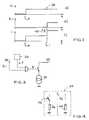
- the digital input 12has an input pad 14 through which signals are fed to the integrated circuit 10, a threshold switch 16 and a pull-down current source 18.
- the threshold switch 16is typically implemented as a Schmitt trigger. Input signals applied to the input pad 14 which exceed the threshold value of the threshold switch 16 are transferred to a digital part 20 of the integrated circuit 10.
- the digital part 20processes the input signals taking into account further signals to one or more digital output signals. Such a digital output signal can be converted via the analog / digital converter 22 into an analog signal and transferred to an output pad 24.
- the digital output signalis formed in particular taking into account the output signal of the threshold value switch 16 and an in-circuit signal S_i which is output by an analogue part 26.
- the analog partis an example of a second subcircuit.
- the in-circuit signal S_iis an example of a signal that occurs inside the integrated circuit 10 but is not directly removable on any of the input pads or output pads of the integrated circuit 10.
- the circuit-internal signal S_i z. B.formed with a certain time delay when a predetermined signal occurs at an analog input 28 of the integrated circuit 10.
- the integrated circuit 10further includes a switchable pull-down current source 30.
- While the pull down power source 18is continuously receiving a first stream from a node 32 pulls the digital input 12, a second current that can pull the second pull down current source 30, only with pull down power source 30 is disconnected from the node 32.
- the two pull-down current sources 18 and 30 interconnected via the node 32together constitute a first sub-circuit 34 of variable current-voltage characteristic having a potential at the input 12, ie at the input pad 14 or node 32, in the absence of an input signal keeps at a defined value.
- the first subcircuit 34has the said variable current-voltage characteristic.
- the first subcircuit 34has a control input 36 for a control signal with which the switchable pull-down current source 30 can be switched on.
- the circuit-internal signal S_i already mentionedserves as a control signal for the first subcircuit 34.
- FIG. 2 ashows the time profile of a voltage signal 38 at the input pad 14, as can be generated by connecting a constant voltage source to the input pad 14.
- the constant voltage sourceis turned on.
- a current iflows from the constant voltage source into the digital input 12 to the node 32.
- the current iexactly replaces the outflows in the threshold switches 16 and in the pull down current source 18.
- the switchable pull down current source 30is initially switched off because at the control input 36 of the first subcircuit 34 is still present no control signal.
- the current ithen adjusts, for example, to a constant value, as shown qualitatively in FIG. 2c between times t_0 and t_1.
- the circuit-internal signal S_iis output from the analog part 26.
- the signal S_imay, however, also be a signal which is formed within the digital part 20 of the integrated circuit 10. As an internal signal this occurs Signal S_i not at inputs or outputs of the integrated circuit 10, so that it can not be detected directly.
- the internal signal S_1is used in the embodiment of FIG. 1 via the control input 36 of the first subcircuit 34 for switching on the switchable pull-down current source 30. Consequently, the switchable pull-down current source 30 is turned on at the occurrence of the in-circuit signal S_i at time t_1.
- the occurrence of the circuit-internal signal S_1 at time t_1is shown in FIG. 2c.
- Switching on the switchable pull-down current source 30changes the voltage characteristic of the first subcircuit 34.
- the switchable pull-down current source 30draws an additional current from the node 32 of the digital input 12.
- the constant voltage source connected to the input pad 14must replace this additional current flowing from the node 32 in order to keep the voltage at the input pad 14 constant.
- the constant voltage sourcemust therefore supply a higher current from the time t_1 than in the period between t_0 and t_1. This higher current flow over the input pad 14 is measurable and qualitatively represented in FIG. 2c by the step-shaped rise 40 at the instant t_1.
- the occurrence of the stage in the current signal itherefore indicates the occurrence of the circuit-internal signal S_i in the interior of the integrated circuit.
- the first subcircuit 34can therefore also be regarded as a test assistance circuit.
- the variation of the input current by switching on the switchable pull-down current source 30is normally unproblematic as long as the specification values of the circuit are maintained.
- the variation of the input currentcan still be influenced by an enable signal S_f.
- a control signal Swhich switches on the switchable pull-down current source 30, is output only if the signal S_i of the analog part 26, which is present at the control input 36, and the enable signal S_f, for example, from the digital part 20 is issued simultaneously. In FIG. 3 this is represented by the AND operation 42.
- first sub-circuit 34instead of pull-down current sources 18 and 30 may also have pull-up power sources.
- FIG. 4shows an alternative first subcircuit 34 with a pull-down resistor 44 which replaces the current source 18 from FIG.
- the switchable pull-down current source 30is replaced from the figure 1 by a switchable pull-down resistor 46, as also shown in Fig. 4.
- the pull down resistors 44, 46can also be replaced by pull up resistors.
Landscapes
- Engineering & Computer Science (AREA)
- General Engineering & Computer Science (AREA)
- Physics & Mathematics (AREA)
- General Physics & Mathematics (AREA)
- Semiconductor Integrated Circuits (AREA)
- Tests Of Electronic Circuits (AREA)
- Logic Circuits (AREA)
Abstract
Description
Translated fromGermanDie Erfindung betrifft eine Integrierte Schaltung, die wenigstens einen digitalen Eingang und eine erste Teilschaltung aufweist, die eine Strom-Spannungs-Charakteristik besitzt und die ein Potenzial an dem Eingang bei fehlendem Eingangssignal auf einem definierten Wert hält, und mit einer zweiten Teilschaltung, die ein schaltungsinternes Signal bereitstellt, dessen Zustand sich nicht unmittelbar an einem Ausgang der Schaltung zeigt. Die Erfindung betrifft ferner ein Verfahren zur Prüfung einer solchen Integrierten Schaltung.The invention relates to an integrated circuit having at least one digital input and a first sub-circuit, which has a current-voltage characteristic and holds a potential at the input in the absence of input signal to a defined value, and a second sub-circuit, the provides in-circuit signal whose state is not directly at an output of the circuit. The invention further relates to a method for testing such an integrated circuit.
Unter einem digitalen Eingang wird dabei ein Eingang mit einem Schwellenwertschalter verstanden, der ein Eingangssignal erst dann an eine interne Signalverarbeitung weiterleitet, wenn das Eingangssignal einen vorgegebenen Schwellenwert überschreitet. Wenn dem Eingang kein Eingangssignal zugeführt wird, können elektromagnetische Einflüsse aus der Umgebung grundsätzlich Potenzialschwankungen an dem Eingang erzeugen, die den Schwellenwert überschreiten. Dies ist unerwünscht. Zur Vermeidung der unerwünschten Zustände dient die genannte Teilschaltung. Die Teilschaltung weist zum Beispiel eine Stromsenke auf, die in der Lage ist, einen Strom vorbestimmter Maximalstärke von dem Eingang zu ziehen. Der Schwellenwert kann erst dann überschritten wenn, wenn ein in den Eingang hineinfließender Signalstrom größer als der Strom der Stromsenke ist. Ein solche auch als Pull Down Stromquelle bezeichnete Stromsenke hält das Potenzial am Eingang auf einem Wert unterhalb des Schwellenwertes fest. Analog hält eine Pull Up Stromquelle das Potenzial oberhalb des Schwellenwerts fest.In this case, a digital input is understood as meaning an input having a threshold value switch, which only forwards an input signal to internal signal processing when the input signal exceeds a predetermined threshold value. If no input signal is supplied to the input, environmental environmental influences may in principle produce potential fluctuations at the input that exceed the threshold. This is undesirable. To avoid the unwanted States serves the said subcircuit. The subcircuit includes, for example, a current sink capable of drawing a current of predetermined maximum magnitude from the input. The threshold value can only be exceeded if a signal current flowing into the input is greater than the current of the current sink. Such a current sink, also referred to as pull-down current source, holds the potential at the input at a value below the threshold value. Likewise, a pull-up power source holds the potential above the threshold.
Im Betrieb Integrierter Schaltung treten Änderungen von Zuständen schaltungsinterner Signale auf, die sich nicht unmittelbar im Verhalten der Eingangssignale und Ausgangssignale der Integrierten Schaltung abbilden. Für eine Funktionsprüfung der Schaltung am Ende eines Fertigungsprozesses kann die Frage, ob und gegebenenfalls zu welchem Zeitpunkt eine solche Zustandsänderung auftritt, wichtig sein. Grundsätzlich kann für das interne Signal ein eigener Anschluss vorgesehen werden, an dem das interne Signal zu Testzwecken abgegriffen werden kann. Bei einer vorgegebenen Schaltung ist die Zahl möglicher Anschlüsse jedoch bereits aus Platzgründen beschränkt. Außerdem stellt jeder Anschluss einen unerwünschten Eingang für Störeinflüsse wie ESD-Impulse dar.In the operation of integrated circuit changes of states of in-circuit signals occur that do not reflect directly in the behavior of the input signals and output signals of the integrated circuit. For a functional test of the circuit at the end of a production process, the question of whether and, if so, at what time such a change in state occurs, may be important. In principle, a separate connection can be provided for the internal signal, at which the internal signal can be tapped for test purposes. For a given circuit, however, the number of possible connections is already limited for reasons of space. In addition, each port is an unwanted input for disturbances such as ESD pulses.
Eine weitere Möglichkeit zur Überprüfung eines internen Signals besteht in der Analyse des Eingangs-Ausgangssignal-Verhaltens der Integrierten Schaltung. Dabei ist jedoch problematisch, dass sich das interne Signal unter Umständen nur sehr indirekt und mit großer zeitlicher Verzögerung in einem regulären Ausgangssignal abbildet, so dass interne Signale nur unvollständig oder mit einem hohen Messzeitaufwand erfasst werden können, was insbesondere bei einer Bandende-Prüfung zu einer Produktionsraten-Verringerung führen kann.Another way to verify an internal signal is to analyze the input-output signal behavior of the integrated circuit. However, it is problematic that the internal signal may be only very indirectly and with a large time delay in a regular output signal, so that internal signals can be detected only incomplete or with a high measurement time, which in particular at a band end check to a Production rate reduction can result.
Eine Schaltung und ein Verfahren der eingangs genannten Art ist jeweils aus der
Wenn ein internes Prüfsignal auf einen Ausgang geschaltet wird, kann das reguläre Ausgangssignal nicht gleichzeitig abgenommen werden. Prüfungen, bei denen das interne Signal und das reguläre Ausgangssignal erforderlich sind, können daher nur nacheinander ausgeführt werden, was die Messzeit erhöht.When an internal test signal is switched to an output, the regular output signal can not be picked up at the same time. Tests that require the internal signal and the regular output signal can therefore only be performed consecutively, which increases the measuring time.
Vor diesem Hintergrund besteht die Aufgabe der Erfindung in der Angabe einer Integrierten Schaltung, die eine Überprüfung von Zuständen interner Signale ohne zusätzliche Anschlüsse und mit einem verringerten Messzeitaufwand erlaubt.Against this background, the object of the invention is the specification of an integrated circuit, which allows a check of states of internal signals without additional connections and with a reduced measurement time.
Diese Aufgabe wird bei einer Integrierten Schaltung der eingangs genannten Art dadurch gelöst, dass die erste Teilschaltung einen Steuereingang für ein Steuersignal aufweist und dazu ausgestaltet ist, ihre Strom-Spannungs-Charakteristik zu ändern, wenn das Steuersignal am Steuereingang anliegt. Ferner wird diese Aufgabe mit einem Verfahren der eingangs genannten Art dadurch gelöst, dass ein elektrisches Prüfsignal an den wenigstens einen Eingang angelegt wird und ein zeitliches Verhalten der Strom-Spannungs-Charakteristik zur Diagnose ausgewertet wird.This object is achieved in an integrated circuit of the type mentioned above in that the first subcircuit has a control input for a control signal and is adapted to change their current-voltage characteristic when the control signal is applied to the control input. Furthermore, this object is achieved by a method of the type mentioned in that an electrical test signal is applied to the at least one input and a temporal behavior of the current-voltage characteristic is evaluated for diagnosis.
Die Teilschaltung ist mit einem ohnehin vorhandenen Eingang gekoppelt. Ihre Strom-Spannungs-Charakteristik ist daher prinzipiell über den Eingang erfassbar. Durch die Änderung der Strom-Spannungs-Charakteristik als Funktion des internen Signals wird die Änderung des Zustandes des internen Signals in ein Signalverhalten an dem Eingang abgebildet und kann ohne zusätzlichen Anschluss ausgelesen werden.The subcircuit is coupled to an already existing input. Their current-voltage characteristic is therefore in principle detectable via the input. By changing the current-voltage characteristic as a function of the internal signal, the change in the state of the internal signal is reflected in a signal behavior at the input and can be read out without an additional connection.
Mit Blick auf Ausgestaltungen der Schaltung ist bevorzugt, dass das schaltungsinterne Signal das Steuersignal ist. Diese Ausgestaltung ist schaltungstechnisch besonders einfach zu realisieren. Entsprechend ist die korrespondierende Verfahrensausgestaltung einfach durchzuführen.With regard to embodiments of the circuit, it is preferred that the circuit-internal signal is the control signal. This refinement is particularly simple to implement in terms of circuitry. Accordingly, the corresponding method design is easy to perform.
Bevorzugt ist auch, dass das Steuersignal das Ergebnis einer UND-Verknüpfung eines Freigabesignals mit dem schaltungsinternen Signal ist. Durch ein solches Freigabesignal kann festgelegt werden, wann die Änderung der Strom-Spannungs-Charakteristik erlaubt ist. Dies ist hilfreich, wenn die Änderung den Normalbetrieb beeinflussen könnte.It is also preferred that the control signal is the result of an AND operation of a Enable signal with the circuit-internal signal is. By means of such an enable signal it can be determined when the change of the current-voltage characteristic is permitted. This is useful if the change could affect normal operation.
Eine weitere Ausgestaltung sieht vor, dass der digitale Eingang eine erste Pull Down Stromquelle aufweist, die einen ersten Strom von einem Eingang eines Schwellenwertschalters zieht und dass die Teilschaltung eine schaltbare Pull Down Stromquelle aufweist, die vom schaltungsinternen Signal geschaltet wird und einen zweiten Strom von dem Eingang des Schwellenwertschalters zieht.A further embodiment provides that the digital input has a first pull-down current source, which draws a first current from an input of a threshold switch and that the sub-circuit has a switchable pull-down current source, which is switched by the circuit-internal signal and a second current of the Input of the threshold switch pulls.
Alternativ ist bevorzugt, dass der digitale Eingang eine erste Pull Up Stromquelle aufweist, die einen ersten Strom an einen Eingang eines Schwellenwertschalters liefert und dass die Teilschaltung eine schaltbare Pull Up Stromquelle aufweist, die vom schaltungsinternen Signal geschaltet wird und einen zweiten Strom an den Eingang des Schwellenwertschalters liefert.Alternatively, it is preferred that the digital input comprises a first pull up current source providing a first current to an input of a threshold switch and the subcircuit having a switchable pull up current source switched by the in circuit signal and a second current to the input of the circuit Threshold switch provides.
Weitere Alternativen sehen vor, dass der digitale Eingang einen ersten Pull Down Widerstand (Pull Up Widerstand) aufweist, der zwischen einem Eingang eines Schwellenwertschalters und einem ersten (zweiten) Bezugspotenzial liegt und dass die Teilschaltung einen schaltbaren Pull Down Widerstand (Pull Up Widerstand) aufweist, der vom schaltungsinternen Signal geschaltet wird und zwischen dem Eingang des Schwellenwertschalters und dem ersten (zweiten) Bezugspotenzial liegt.Other alternatives provide that the digital input has a first pull-down resistor (Pull Up Resistor) that is between an input of a threshold switch and a first (second) reference potential and that the sub-circuit has a switchable pull-down resistor (Pull Up Resistor) which is switched by the in-circuit signal and lies between the input of the threshold switch and the first (second) reference potential.
Diese Ausgestaltungen belegen die breite Verwendbarkeit der Erfindung. Weitere Vorteile ergeben sich aus der Beschreibung und den beigefügten Figuren.These embodiments demonstrate the broad applicability of the invention. Further advantages will become apparent from the description and the accompanying figures.
Es versteht sich, dass die vorstehend genannten und die nachstehend noch zu erläuternden Merkmale nicht nur in der jeweils angegebenen Kombination, sondern auch in anderen Kombinationen oder in Alleinstellung verwendbar sind, ohne den Rahmen der vorliegenden Erfindung zu verlassen.It is understood that the features mentioned above and those yet to be explained below can be used not only in the particular combination given, but also in other combinations or in isolation, without departing from the scope of the present invention.
Ausführungsbeispiele der Erfindung sind in den Zeichnungen dargestellt und werden in der nachfolgenden Beschreibung näher erläutert. Es zeigen, jeweils in schematischer Form:
- Fig. 1
- eine Integrierte Schaltung mit einer ersten Ausgestaltung der Erfindung;
- Fig. 2
- zeitliche Verläufe von Signalen, wie sie in der Ausgestaltung der Fig. 1 bei einer Durchführung des Verfahrens auftreten;
- Fig. 3
- eine Ausgestaltung der Schaltung, die mit einem Freigabesignal arbeitet; und
- Fig. 4
- eine Ausgestaltung der ersten Teilschaltung mit Pull Down Widerständen.
- Fig. 1
- an integrated circuit with a first embodiment of the invention;
- Fig. 2
- time courses of signals, as they occur in the embodiment of Figure 1 in an implementation of the method.
- Fig. 3
- an embodiment of the circuit which operates with an enable signal; and
- Fig. 4
- an embodiment of the first sub-circuit with pull-down resistors.
Im Einzelnen zeigt Figur 1 einen Ausschnitt aus einer integrierten Schaltung 10 mit einem digitalen Eingang 12. Es versteht sich, dass die Integrierte Schaltung 10 im Allgemeinen weitere digitale Eingänge aufweist. Der digitale Eingang 12 besitzt ein Eingangspad 14, über das Signale in die Integrierte Schaltung 10 eingespeist werden, einen Schwellenwertschalter 16 und eine Pull Down Stromquelle 18. Der Schwellenschalter 16 ist in der Regel als Schmitt-Trigger realisiert. Am Eingangspad 14 anliegende Eingangssignale, die den Schwellenwert des Schwellenwertschalters 16 überschreiten, werden an einen Digitalteil 20 der integrierten Schaltung 10 übergeben. Der Digitalteil 20 verarbeitet die Eingangssignale unter Berücksichtigung weiterer Signale zu einem oder mehreren digitalen Ausgangssignalen. Ein solches digitales Ausgangssignal kann über den Analog/Digitalwandler 22 in ein Analogsignal umgewandelt und an ein Ausgangspad 24 übergeben werden.1 shows a detail of an integrated
In der Ausgestaltung der Figur 1 wird das digitale Ausgangssignal insbesondere unter Berücksichtigung des Ausgangssignals des Schwellenwertschalters 16 und eines schaltungsinternen Signals S_i gebildet, das von einem Analogteil 26 ausgegeben wird. Der Analogteil stellt ein Beispiel einer zweiten Teilschaltung dar. Das schaltungsinterne Signal S_i ist ein Beispiel für ein Signal, das im Inneren der integrierten Schaltung 10 auftritt, jedoch nicht direkt an einem der Eingangspads oder Ausgangspads der integrierten Schaltung 10 abnehmbar ist. In der Ausgestaltung der Figur 1 wird das schaltungsinterne Signal S_i z. B. mit einer gewissen Zeitverzögerung dann gebildet, wenn an einem Analogeingang 28 der integrierten Schaltung 10 ein vorbestimmtes Signal auftritt. Die Integrierte Schaltung 10 weist ferner eine schaltbare Pull Down Stromquelle 30 auf.In the embodiment of FIG. 1, the digital output signal is formed in particular taking into account the output signal of the
Während die Pull Down Stromquelle 18 kontinuierlich einen ersten Strom von einem Knoten 32 des digitalen Eingangs 12 zieht, wird ein zweiter Strom, den die zweite Pull Down Stromquelle 30 ziehen kann, nur bei eingeschalteter Pull Down Stromquelle 30 von dem Knoten 32 abgezogen. Die beiden über den Knoten 32 zusammengeschalteten Pull Down Stromquellen 18 und 30 stellen zusammen eine erste Teilschaltung 34 mit veränderlicher Strom-Spannungs-Charakteristik dar, die ein Potenzial an dem Eingang 12, das heißt an dem Eingangspad 14 oder dem Knoten 32, bei fehlendem Eingangssignal auf einem definierten Wert hält.While the pull down
Wenn man an das Eingangspad 14 ein Eingangssignal mit einer konstanten Spannung u anlegt, ändert sich der Signalstrom vom Eingangspad 14 zum Knoten 32 je nachdem, ob die schaltbare Stromquelle 30 eingeschaltet oder ausgeschaltet ist. Insofern besitzt die erste Teilschaltung 34 die genannte veränderliche Strom-Spannungs-Charakteristik. Die erste Teilschaltung 34 weist einen Steuereingang 36 für ein Steuersignal auf, mit dem die schaltbare Pull Down Stromquelle 30 eingeschaltet werden kann. In der Ausgestaltung der Figur 1 dient das bereits genannte schaltungsinterne Signal S_i als Steuersignal für die erste Teilschaltung 34.By applying an input signal to the
Figur 2a zeigt den zeitlichen Verlauf eines Spannungssignals 38 am Eingangspad 14, wie es durch Anschluss einer Konstantspannungsquelle an das Eingangspad 14 erzeugt werden kann. Zum Zeitpunkt t_0 wird die Konstantspannungsquelle eingeschaltet. Dann fließt ein Strom i von der Konstantspannungsquelle in den digitalen Eingang 12 zum Knoten 32. Der Strom i ersetzt genau die Abflüsse in den Schwellenwertschaltern 16 und in die Pull Down Stromquelle 18. Die schaltbare Pull Down Stromquelle 30 ist dabei zunächst ausgeschaltet, weil am Steuereingang 36 der ersten Teilschaltung 34 noch kein Steuersignal anliegt. Der Strom i stellt sich dann zum Beispiel auf einen konstanten Wert ein, wie er qualitativ in der Figur 2c zwischen den Zeiten t_0 und t_1 dargestellt ist.FIG. 2 a shows the time profile of a
Zum Zeitpunkt t_1 tritt dann innerhalb der integrierten Schaltung 10 das schaltungsinterne Signal S_i auf. In der Ausgestaltung der Figur 1 wird das Signal S_i von dem Analogteil 26 ausgegeben. Bei dem Signal S_i kann es sich aber auch um ein Signal handeln, das innerhalb des Digitalteils 20 der integrierten Schaltung 10 gebildet wird. Als internes Signal tritt dieses Signal S_i nicht an Eingängen oder Ausgängen der integrierten Schaltung 10 auf, so dass es nicht direkt detektiert werden kann. Um trotzdem eine Detektion zu ermöglichen, wird das interne Signal S_1 bei der Ausgestaltung der Figur 1 über den Steuereingang 36 der ersten Teilschaltung 34 zum Einschalten der schaltbaren Pull Down Stromquelle 30 genutzt. Folglich wird die schaltbare Pull Down Stromquelle 30 beim Auftreten des schaltungsinternen Signals S_i zum Zeitpunkt t_1 eingeschaltet. Das Auftreten des schaltungsinternen Signals S_1 zum Zeitpunkt t_1 ist in der Fig. 2c dargestellt.At the time t_1 then occurs within the integrated
Durch das Einschalten der schaltbaren Pull Down Stromquelle 30 ändert sich die Spannungscharakteristik der ersten Teilschaltung 34. Die schaltbare Pull Down Stromquelle 30 zieht einen zusätzlichen Strom von dem Knoten 32 des digitalen Eingangs 12 ab. Die an dem Eingangspad 14 angeschlossene Konstantspannungsquelle muss diesen zusätzlich vom Knoten 32 abfließenden Strom ersetzen, um die Spannung am Eingangspad 14 konstant zu halten. Die Konstantspannungsquelle muss daher ab dem Zeitpunkt t_1 einen höheren Strom liefern als im Zeitraum zwischen t_0 und t_1. Dieser höhere Stromfluss über den Eingangspad 14 ist messbar und in der Figur 2c qualitativ durch den stufenförmigen Anstieg 40 zum Zeitpunkt t_1 dargestellt. Das Auftreten der Stufe im Stromsignal i zeigt daher das Auftreten des schaltungsinternen Signals S_i im Inneren der integrierten Schaltung an.Switching on the switchable pull-down
Die erste Teilschaltung 34 kann daher auch als Testhilfe-Schaltung betrachtet werden. Die Variation des Eingangsstroms durch Zuschalten der schaltbaren Pull Down Stromquelle 30 ist normalerweise unproblematisch, solange die Spezifikationswerte der Schaltung eingehalten werden. Die Variation des Eingangsstroms kann in einer Ausgestaltung der Figur 1, wie sie ausschnittsweise in der Figur 3 dargestellt ist, noch durch ein Freigabesignal S_f beeinflusst werden. In der Ausgestaltung der Figur 3 wird ein Steuersignal S, das die schaltbare Pull Down Stromquelle 30 zuschaltet, nur dann ausgegeben, wenn gleichzeitig das Signal S_i des Analogteils 26, das am Steuereingang 36 anliegt, und das Freigabesignal S_f, das bspw. von dem Digitalteil 20 ausgegeben wird, gleichzeitig vorliegen. In der Figur 3 wird dies durch die UND-Verknüpfung 42 repräsentiert.The
Es versteht sich, dass die erste Teilschaltung 34 anstelle von Pull Down Stromquellen 18 und 30 auch Pull Up Stromquellen aufweisen kann. Eine weitere Alternative ist in der Figur 4 dargestellt. Figur 4 zeigt eine alternative erste Teilschaltung 34 mit einem einen Pull Down Widerstand 44, der die Stromquelle 18 aus der Figur 1 ersetzt. In diesem Fall wird die schaltbare Pull Down Stromquelle 30 aus der Figur 1 durch einen schaltbaren Pull Down Widerstand 46 ersetzt, wie er ebenfalls in der Fig. 4 dargestellt ist. Die Pull Down Widerstände 44, 46 können auch durch Pull Up Widerstände ersetzt werden.It is understood that the first sub-circuit 34 instead of pull-down
Claims (10)
Translated fromGermanApplications Claiming Priority (1)
| Application Number | Priority Date | Filing Date | Title |
|---|---|---|---|
| DE102005052269ADE102005052269A1 (en) | 2005-10-27 | 2005-10-27 | Integrated circuit with integrated test help subcircuit |
Publications (2)
| Publication Number | Publication Date |
|---|---|
| EP1783779A1true EP1783779A1 (en) | 2007-05-09 |
| EP1783779B1 EP1783779B1 (en) | 2008-07-02 |
Family
ID=37684904
Family Applications (1)
| Application Number | Title | Priority Date | Filing Date |
|---|---|---|---|
| EP06022111AExpired - Fee RelatedEP1783779B1 (en) | 2005-10-27 | 2006-10-21 | Integrated circuit with integrated test aid sub-circuit |
Country Status (3)
| Country | Link |
|---|---|
| US (1) | US7535245B2 (en) |
| EP (1) | EP1783779B1 (en) |
| DE (2) | DE102005052269A1 (en) |
Families Citing this family (1)
| Publication number | Priority date | Publication date | Assignee | Title |
|---|---|---|---|---|
| US8255707B2 (en)* | 2008-03-06 | 2012-08-28 | Fujitsu Limited | System and method for providing a one-step testing architecture |
Citations (6)
| Publication number | Priority date | Publication date | Assignee | Title |
|---|---|---|---|---|
| US5132937A (en)* | 1989-06-01 | 1992-07-21 | Mitsubishi Denki Kabushiki Kaisha | Semiconductor memory device having on-chip test circuit and operating method thereof |
| US5600271A (en)* | 1995-09-15 | 1997-02-04 | Xilinx, Inc. | Input signal interface with independently controllable pull-up and pull-down circuitry |
| US6356105B1 (en)* | 2000-06-28 | 2002-03-12 | Intel Corporation | Impedance control system for a center tapped termination bus |
| DE10064478A1 (en)* | 2000-12-22 | 2002-07-04 | Atmel Germany Gmbh | Method for testing an integrated circuit |
| US20030160620A1 (en)* | 2002-02-25 | 2003-08-28 | Miesterfeld Frederick O. | Addressable open connector test circuit |
| US6624656B1 (en)* | 1999-10-15 | 2003-09-23 | Triscend Corporation | Input/output circuit with user programmable functions |
Family Cites Families (3)
| Publication number | Priority date | Publication date | Assignee | Title |
|---|---|---|---|---|
| JP2000012639A (en)* | 1998-06-24 | 2000-01-14 | Toshiba Corp | Monitor TEG test circuit |
| DE10134215B4 (en)* | 2001-07-13 | 2004-08-05 | Infineon Technologies Ag | Method for switching from a first operating state of an integrated circuit to a second operating state of the integrated circuit and integrated circuit with a circuit arrangement for switching |
| US6940271B2 (en)* | 2001-08-17 | 2005-09-06 | Nptest, Inc. | Pin electronics interface circuit |
- 2005
- 2005-10-27DEDE102005052269Apatent/DE102005052269A1/ennot_activeCeased
- 2006
- 2006-10-21DEDE502006001021Tpatent/DE502006001021D1/enactiveActive
- 2006-10-21EPEP06022111Apatent/EP1783779B1/ennot_activeExpired - Fee Related
- 2006-10-26USUS11/586,710patent/US7535245B2/enactiveActive
Patent Citations (6)
| Publication number | Priority date | Publication date | Assignee | Title |
|---|---|---|---|---|
| US5132937A (en)* | 1989-06-01 | 1992-07-21 | Mitsubishi Denki Kabushiki Kaisha | Semiconductor memory device having on-chip test circuit and operating method thereof |
| US5600271A (en)* | 1995-09-15 | 1997-02-04 | Xilinx, Inc. | Input signal interface with independently controllable pull-up and pull-down circuitry |
| US6624656B1 (en)* | 1999-10-15 | 2003-09-23 | Triscend Corporation | Input/output circuit with user programmable functions |
| US6356105B1 (en)* | 2000-06-28 | 2002-03-12 | Intel Corporation | Impedance control system for a center tapped termination bus |
| DE10064478A1 (en)* | 2000-12-22 | 2002-07-04 | Atmel Germany Gmbh | Method for testing an integrated circuit |
| US20030160620A1 (en)* | 2002-02-25 | 2003-08-28 | Miesterfeld Frederick O. | Addressable open connector test circuit |
Also Published As
| Publication number | Publication date |
|---|---|
| DE102005052269A1 (en) | 2007-05-10 |
| DE502006001021D1 (en) | 2008-08-14 |
| EP1783779B1 (en) | 2008-07-02 |
| US20070096960A1 (en) | 2007-05-03 |
| US7535245B2 (en) | 2009-05-19 |
Similar Documents
| Publication | Publication Date | Title |
|---|---|---|
| DE69733789T2 (en) | High resolution power supply test system | |
| DE102019121794A1 (en) | INTELLIGENT ELECTRONIC SWITCH | |
| EP3111284B1 (en) | Input circuit that can be made redundant, input circuit unit having at least one input circuit, and method for operating such an input circuit unit | |
| EP3740771B1 (en) | Electrical circuit for testing primary internal signals on an asic | |
| WO2014009207A1 (en) | Apparatus for diagnosing a circuit arrangement | |
| DE102019132242B4 (en) | Uses of a circuit arrangement with active measuring voltage to determine an insulation resistance in one or more ungrounded power supply system (s) | |
| EP3649476B1 (en) | Device and method for checking the functionality of a system resistor of a battery system | |
| EP2616827B1 (en) | Apparatus for monitoring operating parameters of integrated circuits and integrated circuit with operating parameter monitoring | |
| DE10064478B4 (en) | Method for testing an integrated circuit and circuit arrangement | |
| EP3436834B1 (en) | Arrangement with at least two redundant analog input units for a measuring current | |
| DE102005016127B4 (en) | sensor system | |
| EP1783779B1 (en) | Integrated circuit with integrated test aid sub-circuit | |
| DE20101605U1 (en) | Device for providing an input signal for a line mismatched on the output side | |
| EP3404430B1 (en) | Method for monitoring an operation of a binary interface and related binary interface | |
| DE3715163A1 (en) | ELECTRICAL TEST CIRCUIT | |
| EP0757254A2 (en) | Integrated circuit | |
| DE102017208171B3 (en) | Method for monitoring operation of a binary interface and corresponding binary interface | |
| EP4361651B1 (en) | Operating device with functional monitoring of the detection of the switching state of at least one associated operable switching element, associated use and method | |
| EP3701276A1 (en) | Integrated circuit and asic | |
| DE102005059489B4 (en) | Circuit and method for input signal determination | |
| DE4303048A1 (en) | Alarm recognition apparatus for redundant layout circuit in radio equipment - has input circuits delaying alarm recognition signals when circuits are switched to be operational systems | |
| EP3997466A1 (en) | Device for measuring the current and voltage of an input signal | |
| DE202014010494U1 (en) | measuring device | |
| DE102010031096A1 (en) | Method for testing production mistakes and increased leakage currents in semiconductor circuit utilized in integrated circuit, involves outputting error signal when remaining voltage is ramped down faster than predetermined wave speed | |
| DE102004012267A1 (en) | A sensor for measuring physical quantities and for passing the measured quantity, a circuit comprising such a sensor and methods for operating the sensor and the circuit |
Legal Events
| Date | Code | Title | Description |
|---|---|---|---|
| PUAI | Public reference made under article 153(3) epc to a published international application that has entered the european phase | Free format text:ORIGINAL CODE: 0009012 | |
| 17P | Request for examination filed | Effective date:20061021 | |
| AK | Designated contracting states | Kind code of ref document:A1 Designated state(s):AT BE BG CH CY CZ DE DK EE ES FI FR GB GR HU IE IS IT LI LT LU LV MC NL PL PT RO SE SI SK TR | |
| AX | Request for extension of the european patent | Extension state:AL BA HR MK YU | |
| AKX | Designation fees paid | Designated state(s):DE FR | |
| GRAP | Despatch of communication of intention to grant a patent | Free format text:ORIGINAL CODE: EPIDOSNIGR1 | |
| GRAS | Grant fee paid | Free format text:ORIGINAL CODE: EPIDOSNIGR3 | |
| GRAA | (expected) grant | Free format text:ORIGINAL CODE: 0009210 | |
| AK | Designated contracting states | Kind code of ref document:B1 Designated state(s):DE FR | |
| REF | Corresponds to: | Ref document number:502006001021 Country of ref document:DE Date of ref document:20080814 Kind code of ref document:P | |
| PLBE | No opposition filed within time limit | Free format text:ORIGINAL CODE: 0009261 | |
| STAA | Information on the status of an ep patent application or granted ep patent | Free format text:STATUS: NO OPPOSITION FILED WITHIN TIME LIMIT | |
| 26N | No opposition filed | Effective date:20090403 | |
| PGFP | Annual fee paid to national office [announced via postgrant information from national office to epo] | Ref country code:FR Payment date:20091110 Year of fee payment:4 | |
| PGFP | Annual fee paid to national office [announced via postgrant information from national office to epo] | Ref country code:DE Payment date:20101027 Year of fee payment:5 | |
| PG25 | Lapsed in a contracting state [announced via postgrant information from national office to epo] | Ref country code:FR Free format text:LAPSE BECAUSE OF NON-PAYMENT OF DUE FEES Effective date:20101102 | |
| REG | Reference to a national code | Ref country code:FR Ref legal event code:ST Effective date:20110630 | |
| PG25 | Lapsed in a contracting state [announced via postgrant information from national office to epo] | Ref country code:DE Free format text:LAPSE BECAUSE OF NON-PAYMENT OF DUE FEES Effective date:20120501 | |
| REG | Reference to a national code | Ref country code:DE Ref legal event code:R119 Ref document number:502006001021 Country of ref document:DE Effective date:20120501 |