EP1766697B1 - Light emitting devices having current blocking structures and methods of fabricating light emitting devices having current blocking structures - Google Patents
Light emitting devices having current blocking structures and methods of fabricating light emitting devices having current blocking structuresDownload PDFInfo
- Publication number
- EP1766697B1 EP1766697B1EP05763653AEP05763653AEP1766697B1EP 1766697 B1EP1766697 B1EP 1766697B1EP 05763653 AEP05763653 AEP 05763653AEP 05763653 AEP05763653 AEP 05763653AEP 1766697 B1EP1766697 B1EP 1766697B1
- Authority
- EP
- European Patent Office
- Prior art keywords
- region
- active region
- bond pad
- light emitting
- contact
- Prior art date
- Legal status (The legal status is an assumption and is not a legal conclusion. Google has not performed a legal analysis and makes no representation as to the accuracy of the status listed.)
- Expired - Lifetime
Links
- 238000000034methodMethods0.000titleclaimsabstractdescription10
- 230000000903blocking effectEffects0.000titleabstractdescription11
- 239000004065semiconductorSubstances0.000claimsabstractdescription34
- 229910052751metalInorganic materials0.000claimsdescription26
- 239000002184metalSubstances0.000claimsdescription26
- 239000000463materialSubstances0.000claimsdescription15
- 238000004519manufacturing processMethods0.000claimsdescription9
- BASFCYQUMIYNBI-UHFFFAOYSA-NplatinumChemical compound[Pt]BASFCYQUMIYNBI-UHFFFAOYSA-N0.000claims4
- 229910052697platinumInorganic materials0.000claims2
- 230000007246mechanismEffects0.000abstractdescription6
- 239000010410layerSubstances0.000description70
- 239000000758substrateSubstances0.000description27
- 229910002601GaNInorganic materials0.000description17
- JMASRVWKEDWRBT-UHFFFAOYSA-NGallium nitrideChemical compound[Ga]#NJMASRVWKEDWRBT-UHFFFAOYSA-N0.000description10
- HBMJWWWQQXIZIP-UHFFFAOYSA-Nsilicon carbideChemical compound[Si+]#[C-]HBMJWWWQQXIZIP-UHFFFAOYSA-N0.000description10
- 229910010271silicon carbideInorganic materials0.000description10
- IJGRMHOSHXDMSA-UHFFFAOYSA-NAtomic nitrogenChemical compoundN#NIJGRMHOSHXDMSA-UHFFFAOYSA-N0.000description8
- 239000007943implantSubstances0.000description7
- 150000004767nitridesChemical class0.000description6
- XUIMIQQOPSSXEZ-UHFFFAOYSA-NSiliconChemical compound[Si]XUIMIQQOPSSXEZ-UHFFFAOYSA-N0.000description5
- 229910052710siliconInorganic materials0.000description5
- 239000010703siliconSubstances0.000description5
- JBRZTFJDHDCESZ-UHFFFAOYSA-NAsGaChemical compound[As]#[Ga]JBRZTFJDHDCESZ-UHFFFAOYSA-N0.000description4
- 229910001218Gallium arsenideInorganic materials0.000description4
- 150000001875compoundsChemical class0.000description4
- 229910052757nitrogenInorganic materials0.000description4
- 229910052594sapphireInorganic materials0.000description4
- 239000010980sapphireSubstances0.000description4
- 229910002704AlGaNInorganic materials0.000description3
- 238000002347injectionMethods0.000description3
- 239000007924injectionSubstances0.000description3
- 238000004377microelectronicMethods0.000description3
- 239000000203mixtureSubstances0.000description3
- 230000006798recombinationEffects0.000description3
- 238000005215recombinationMethods0.000description3
- 238000003892spreadingMethods0.000description3
- 229910005540GaPInorganic materials0.000description2
- VYPSYNLAJGMNEJ-UHFFFAOYSA-NSilicium dioxideChemical compoundO=[Si]=OVYPSYNLAJGMNEJ-UHFFFAOYSA-N0.000description2
- 238000011161developmentMethods0.000description2
- 230000018109developmental processEffects0.000description2
- 238000000605extractionMethods0.000description2
- 238000002513implantationMethods0.000description2
- 238000005468ion implantationMethods0.000description2
- 239000011777magnesiumSubstances0.000description2
- 238000001429visible spectrumMethods0.000description2
- GYHNNYVSQQEPJS-UHFFFAOYSA-NGalliumChemical compound[Ga]GYHNNYVSQQEPJS-UHFFFAOYSA-N0.000description1
- FYYHWMGAXLPEAU-UHFFFAOYSA-NMagnesiumChemical compound[Mg]FYYHWMGAXLPEAU-UHFFFAOYSA-N0.000description1
- OAICVXFJPJFONN-UHFFFAOYSA-NPhosphorusChemical compound[P]OAICVXFJPJFONN-UHFFFAOYSA-N0.000description1
- 238000010521absorption reactionMethods0.000description1
- 229910045601alloyInorganic materials0.000description1
- 239000000956alloySubstances0.000description1
- 229910052782aluminiumInorganic materials0.000description1
- XAGFODPZIPBFFR-UHFFFAOYSA-NaluminiumChemical compound[Al]XAGFODPZIPBFFR-UHFFFAOYSA-N0.000description1
- 230000015572biosynthetic processEffects0.000description1
- 239000000969carrierSubstances0.000description1
- 229910052681coesiteInorganic materials0.000description1
- 230000001427coherent effectEffects0.000description1
- 239000012141concentrateSubstances0.000description1
- 229910052906cristobaliteInorganic materials0.000description1
- 230000000694effectsEffects0.000description1
- 238000005516engineering processMethods0.000description1
- 229910052733galliumInorganic materials0.000description1
- HZXMRANICFIONG-UHFFFAOYSA-Ngallium phosphideChemical compound[Ga]#PHZXMRANICFIONG-UHFFFAOYSA-N0.000description1
- 229910052738indiumInorganic materials0.000description1
- APFVFJFRJDLVQX-UHFFFAOYSA-Nindium atomChemical compound[In]APFVFJFRJDLVQX-UHFFFAOYSA-N0.000description1
- 239000011810insulating materialSubstances0.000description1
- 238000002955isolationMethods0.000description1
- 229910052749magnesiumInorganic materials0.000description1
- 229910001092metal group alloyInorganic materials0.000description1
- 238000012986modificationMethods0.000description1
- 230000004048modificationEffects0.000description1
- 230000003287optical effectEffects0.000description1
- 238000002161passivationMethods0.000description1
- 230000000737periodic effectEffects0.000description1
- 230000005855radiationEffects0.000description1
- 239000000377silicon dioxideSubstances0.000description1
- 239000002356single layerSubstances0.000description1
- 239000007787solidSubstances0.000description1
- 229910052682stishoviteInorganic materials0.000description1
- 229910052905tridymiteInorganic materials0.000description1
- 230000005641tunnelingEffects0.000description1
Images


Classifications
- H—ELECTRICITY
- H10—SEMICONDUCTOR DEVICES; ELECTRIC SOLID-STATE DEVICES NOT OTHERWISE PROVIDED FOR
- H10H—INORGANIC LIGHT-EMITTING SEMICONDUCTOR DEVICES HAVING POTENTIAL BARRIERS
- H10H20/00—Individual inorganic light-emitting semiconductor devices having potential barriers, e.g. light-emitting diodes [LED]
- H10H20/80—Constructional details
- H10H20/83—Electrodes
- H—ELECTRICITY
- H10—SEMICONDUCTOR DEVICES; ELECTRIC SOLID-STATE DEVICES NOT OTHERWISE PROVIDED FOR
- H10H—INORGANIC LIGHT-EMITTING SEMICONDUCTOR DEVICES HAVING POTENTIAL BARRIERS
- H10H20/00—Individual inorganic light-emitting semiconductor devices having potential barriers, e.g. light-emitting diodes [LED]
- H10H20/80—Constructional details
- H10H20/81—Bodies
- H10H20/816—Bodies having carrier transport control structures, e.g. highly-doped semiconductor layers or current-blocking structures
- H10H20/8162—Current-blocking structures
- H—ELECTRICITY
- H01—ELECTRIC ELEMENTS
- H01S—DEVICES USING THE PROCESS OF LIGHT AMPLIFICATION BY STIMULATED EMISSION OF RADIATION [LASER] TO AMPLIFY OR GENERATE LIGHT; DEVICES USING STIMULATED EMISSION OF ELECTROMAGNETIC RADIATION IN WAVE RANGES OTHER THAN OPTICAL
- H01S5/00—Semiconductor lasers
- H01S5/04—Processes or apparatus for excitation, e.g. pumping, e.g. by electron beams
- H01S5/042—Electrical excitation ; Circuits therefor
- H01S5/0421—Electrical excitation ; Circuits therefor characterised by the semiconducting contacting layers
- H—ELECTRICITY
- H01—ELECTRIC ELEMENTS
- H01S—DEVICES USING THE PROCESS OF LIGHT AMPLIFICATION BY STIMULATED EMISSION OF RADIATION [LASER] TO AMPLIFY OR GENERATE LIGHT; DEVICES USING STIMULATED EMISSION OF ELECTROMAGNETIC RADIATION IN WAVE RANGES OTHER THAN OPTICAL
- H01S5/00—Semiconductor lasers
- H01S5/20—Structure or shape of the semiconductor body to guide the optical wave ; Confining structures perpendicular to the optical axis, e.g. index or gain guiding, stripe geometry, broad area lasers, gain tailoring, transverse or lateral reflectors, special cladding structures, MQW barrier reflection layers
- H01S5/2054—Methods of obtaining the confinement
- H01S5/2059—Methods of obtaining the confinement by means of particular conductivity zones, e.g. obtained by particle bombardment or diffusion
- H01S5/2063—Methods of obtaining the confinement by means of particular conductivity zones, e.g. obtained by particle bombardment or diffusion obtained by particle bombardment
- H—ELECTRICITY
- H01—ELECTRIC ELEMENTS
- H01S—DEVICES USING THE PROCESS OF LIGHT AMPLIFICATION BY STIMULATED EMISSION OF RADIATION [LASER] TO AMPLIFY OR GENERATE LIGHT; DEVICES USING STIMULATED EMISSION OF ELECTROMAGNETIC RADIATION IN WAVE RANGES OTHER THAN OPTICAL
- H01S5/00—Semiconductor lasers
- H01S5/20—Structure or shape of the semiconductor body to guide the optical wave ; Confining structures perpendicular to the optical axis, e.g. index or gain guiding, stripe geometry, broad area lasers, gain tailoring, transverse or lateral reflectors, special cladding structures, MQW barrier reflection layers
- H01S5/2054—Methods of obtaining the confinement
- H01S5/2059—Methods of obtaining the confinement by means of particular conductivity zones, e.g. obtained by particle bombardment or diffusion
- H01S5/2068—Methods of obtaining the confinement by means of particular conductivity zones, e.g. obtained by particle bombardment or diffusion obtained by radiation treatment or annealing
- H—ELECTRICITY
- H01—ELECTRIC ELEMENTS
- H01S—DEVICES USING THE PROCESS OF LIGHT AMPLIFICATION BY STIMULATED EMISSION OF RADIATION [LASER] TO AMPLIFY OR GENERATE LIGHT; DEVICES USING STIMULATED EMISSION OF ELECTROMAGNETIC RADIATION IN WAVE RANGES OTHER THAN OPTICAL
- H01S5/00—Semiconductor lasers
- H01S5/30—Structure or shape of the active region; Materials used for the active region
- H01S5/32—Structure or shape of the active region; Materials used for the active region comprising PN junctions, e.g. hetero- or double- heterostructures
- H01S5/323—Structure or shape of the active region; Materials used for the active region comprising PN junctions, e.g. hetero- or double- heterostructures in AIIIBV compounds, e.g. AlGaAs-laser, InP-based laser
- H01S5/32308—Structure or shape of the active region; Materials used for the active region comprising PN junctions, e.g. hetero- or double- heterostructures in AIIIBV compounds, e.g. AlGaAs-laser, InP-based laser emitting light at a wavelength less than 900 nm
- H01S5/32341—Structure or shape of the active region; Materials used for the active region comprising PN junctions, e.g. hetero- or double- heterostructures in AIIIBV compounds, e.g. AlGaAs-laser, InP-based laser emitting light at a wavelength less than 900 nm blue laser based on GaN or GaP
Definitions
- This inventionrelates to semiconductor light emitting diodes and fabricating methods therefor.
- a semiconductor light emitting deviceincludes a semiconductor light emitting element having one or more semiconductor layers that are configured to emit coherent and/or incoherent light upon energization thereof.
- a light emitting diode or laser diodegenerally includes a diode region on a microelectronic substrate.
- the microelectronic substratemay be, for example, gallium arsenide, gallium phosphide, alloys thereof, silicon carbide and/or sapphire.
- LEDsthat are fabricated in or on silicon carbide, because these LEDs can emit radiation in the blue/green portions of the visible spectrum. See, for example, U.S. Patent 5,416,342 to Edmond et al. , entitled Blue Light-Emirting Diode With High External Quantum Efficiency, assigned to the assignee of the present application.
- LEDsthat include gallium nitride-based diode regions on silicon carbide substrates, because these devices also may emit light with high efficiency. See, for example, U.S. Patent 6,177,688 to Linthicum et al. . entitled Pendeoepitaxial Gallium Nitride Semiconductor Layers On Silicon Carbide Substrates.
- the efficiency of conventional LEDsmay be limited by their inability to emit all of the light that is generated by their active region.
- light emitting from its active regionmay be prevented from exiting the LED by, for example, a light absorbing wire bond pad.
- a current spreading contact layeris provided to improve the uniformity of carrier injection across the cross section of the light emitting device. Current is injected into the p-side of the LED through the bond pad and the p-type contact. Light generated in an active region of the device is proportional to the carrier injection.
- substantially uniform photon emission across the active regionmay result from the use of a current spreading layer, such as a substantially transparent p-type contact layer.
- a wire bond padis typically not a transparent structure and, therefore, photons emitted from the active region of the LED that are incident upon the wire bond pad may be absorbed by the wire bond pad. For example, in some instances approximately 70% of the light incident on the wire bond pad may be absorbed. Such photon absorption may reduce the amount of light that escapes from the LED and may decrease the efficiency of the LED.
- Lee et alin an article entitled Characteristics of Top-Surface-Emitting GaAs Quantum-Well Lasers (IEEE Photonics Technology Letters, 2 No.9 September 1990 ) discloses self-aligned, top-surface-emitting, vertical-cavity, GaAs four-quantum-well lasers in which deep buried damaged layers formed by proton implantation are used to control vertical conductivity profiles for efficient current injection at the active region.
- the light outputis through an output window formed in an Au/Zn electrode formed on the surface of the active region. Vertical damaged areas concentrate the current in the active region below the output window.
- WO 03/061021discloses nitride-based semiconductor structures with a ring p-doped contact, in which ion implantation is used to confine the current by selectively disordering the region adjacent the contacts, thus avoiding the emission of light beneath the contacts.
- US-A-2004/0066820discloses a single mode vertical cavity surface emitting laser (VCSEL) wherein a multi-quantum well active region is located between upper and lower mirrors, insulating layers being formed over the upper mirror, light from the active region being caused to pass through an aperture in the insulating layers, an equipotential layer above the insulating layers and dielectric layers on the surface of the laser. Upper electrical contacts are positioned on the surface of the equipotential layer, with isolation regions below them.
- VCSELs having similar current confinement structures formed by ion implantationare disclosed in WO 03/058772 A2 .
- US-A-5245622discloses vertical-cavity surface-emitting lasers wherein light from the active region passes through a stratified electrode comprising high and low doped layers and through a dielectric upper mirror on the surface of the stratified electrode. Electrical contacts are also positioned on the surface of the stratified electrodes, and blocking regions adjacent the active region are positioned below these contacts to confine the current, and hence the light emission, to a region below the upper mirror.
- the active regionincludes a Group III-nitride based active region.
- the insulating regionmay also be a region that is not light absorbing.
- the insulating regionsmay include an implanted region.
- first, second, etc.may be used herein to describe various elements, components, regions, layers and/or sections, these elements, components, regions, layers and/or sections should not be limited by these terms. These terms are only used to distinguish one element, component, region, layer or section from another region, layer or section. Thus, a first element, component, region, layer or section discussed below could be termed a second element, component, region, layer or section without departing from the teachings of the present invention.
- relative termssuch as “lower” or “bottom” and “upper” or “top,” may be used herein to describe one element's relationship to another elements as illustrated in the Figures. It will be understood that relative terms are intended to encompass different orientations of the device in addition to the orientation depicted in the Figures. For example, if the device in the Figures is turned over, elements described as being on the “lower” side of other elements would then be oriented on “upper” sides of the other elements. The exemplary term “lower”, can therefore, encompasses both an orientation of “lower” and “upper,” depending on the particular orientation of the figure.
- Embodiments of the present inventionare described herein with reference to cross-section illustrations that are schematic illustrations of idealized embodiments of the present invention. As such, variations from the shapes of the illustrations as a result, for example, of manufacturing techniques and/or tolerances, are to be expected. Thus, embodiments of the present invention should not be construed as limited to the particular shapes of regions illustrated herein but are to include deviations in shapes that result, for example, from manufacturing. For example, an etched region illustrated or described as a rectangle will, typically, have rounded or curved features. Thus, the regions illustrated in the figures are schematic in nature and their shapes are not intended to illustrate the precise shape of a region of a device and are not intended to limit the scope of the present invention.
- references to a structure or feature that is disposed "adjacent" another featuremay have portions that overlap or underlie the adjacent feature.
- LEDs disclosed hereininclude a substrate
- the crystalline epitaxial growth substrate on which the epitaxial layers comprising an LED are grownmay be removed, and the freestanding epitaxial layers may be mounted on a substitute carrier substrate or submount which may have better thermal, electrical, structural and/or optical characteristics than the original substrate.
- the invention described hereinis not limited to structures having crystallize epitaxial growth substrates and may be utilized in connection with structures in which the epitaxial layers have been removed from their original growth substrates and bonded to substitute carrier substrates.
- Some embodiments of the present inventionmay provide for improved efficacy of a light emitting device by reducing and/or preventing current flow in an active region of the device in a region beneath a wire bond pad or other light absorbing structure.
- some embodiments of the present inventionmay provide light emitting devices and methods of fabricating light emitting devices having a current blocking mechanism below the wire bond pad. By reducing and/or preventing current from being injected directly beneath the wire bond pad, the current may be more likely to be converted to photon emission in areas of the device not under the wire bond pad. Thus, there may be a reduced probability of light being absorbed by the wire bond pad.
- an increase in efficiency of a light emitting device according to some embodiments of the present inventionmay be proportional to the size of the wire bond pad.
- Embodiments of the present inventionmay be particularly well suited for use in nitride-based light emitting devices such as Group III-nitride based devices.
- Group III nitriderefers to those semiconducting compounds formed between nitrogen and the elements in Group III of the periodic table, usually aluminum (Al), gallium (Ga), and/or indium (In).
- Alaluminum
- Gagallium
- Inindium
- the termalso refers to ternary and quaternary compounds such as AlGaN and AlInGaN.
- the Group III elementscan combine with nitrogen to form binary (e.g ., GaN), ternary (e.g ., AlGaN, AlInN), and quaternary (e.g ., AlInGaN) compounds. These compounds all have empirical formulas in which one mole of nitrogen is combined with a total of one mole of the Group III elements. Accordingly, formulas such as Al x Ga 1-x N where 0 ⁇ x ⁇ 1 are often used to describe them.
- embodiments of the present inventionare described herein with reference to Group III-nitride based light emitting devices, such as gallium nitride based light emitting devices, certain embodiments of the present invention may be suitable for use in other semiconductor light emitting devices, such as for example, GaAs and/or GaP based devices.
- Light emitting diodesinclude a light emitting diode which includes one or more semiconductor layers, which may include silicon, silicon carbide, gallium nitride and/or other semiconductor materials, a substrate which may include sapphire, silicon, silicon carbide and/or other microelectronic substrates, and one or more contact layers which may include metal and/or other conductive layers.
- semiconductor layerswhich may include silicon, silicon carbide, gallium nitride and/or other semiconductor materials
- a substratewhich may include sapphire, silicon, silicon carbide and/or other microelectronic substrates
- contact layerswhich may include metal and/or other conductive layers.
- ultraviolet, blue and/or green LEDsmay be provided.
- the design and fabrication of semiconductor light emitting devicesare well known to those having skill in the art and need not be described in detail herein.
- light emitting devicesmay include structures such as the gallium nitride-based LED and/or laser structures fabricated on a silicon carbide substrate such as those devices manufactured and sold by Cree, Inc. of Durham, North Carolina.
- the present inventionmay be suitable for use with LED and/or laser structures that provide active regions such as described in United States Patent Nos.
- the LEDs and/or lasersmay be configured to operate such that light emission occurs through the substrate.
- the substratemay be patterned so as to enhance light output of the devices as is described, for example, in the above-cited U.S. Patent Publication No. US 2002/0123164 A1 .
- These structuresmay be modified as described herein to provide blocking structures according to some embodiments of the present invention.
- embodiments of the present inventionmay be utilized with light emitting devices having bond pads of differing shapes or sizes.
- the light emitting devicesmay be on differing substrates, such as silicon carbide, sapphire, gallium nitride, silicon or other substrate suitable for providing Group III-nitride devices.
- the light emitting devicesmay be suitable for subsequent singulation and mounting on a suitable carrier.
- the light emitting devicesmay include, for example, single quantum well, multi-quantum well and/or bulk active region devices.
- Some embodiments of the present inventionmay be used with devices utilizing a tunneling contact on the p-side of the device.
- Figure 1is a cross-sectional schematic illustration of a light emitting device according to some embodiments of the present invention.
- a substrate 10such as an n-type silicon carbide substrate, has an optional n-type semiconductor layer 12, such as a gallium nitride based layer, provided thereon.
- the n-type semiconductor layer 12may include multiple layers, for example, buffer layers or the like.
- the n-type semiconductor layer 12is provided as a silicon doped AlGaN layer, that may be of uniform or gradient composition, and a silicon doped GaN layer.
- the contact 20may be located, for example, in a recess that contacts the n-type semiconductor layer 12, so as to provide a second contact for the device.
- Other configurationsmay also be utilized.
- an active region 14, such as a single or double heterostructure, quantum well, multi-quantum well or other such active regionmay be provided on the n-type semiconductor layer.
- the term "active region”refers to a region of semiconductor material of a light emitting device, that may be one or more layers and/or portions thereof, where a substantial portion of the photons emitted by the device when in operation are generated by carrier recombination.
- the active regionrefers to a region where substantially all of the photons emitted by the device are generated by carrier recombination.
- the p-ype semiconductor material layer 16may, for example, be a gallium nitride based layer, such as a GaN layer.
- the p-type semiconductor layer 16includes magnesium doped GaN.
- the p-type semiconductor layer 16may include one or multiple layers and may be of uniform or gradient composition.
- a first contact metal layer 18 of contact metal that provides an ohmic contact to the p-type semiconductor material layer 16is also provided.
- the first contact metal layer 18may function as a current spreading layer.
- the first contact metal layer 18may be Pt.
- the first contact metal layer 18is light permeable and in some embodiments is substantially transparent.
- the first contact metal layer 18may be a relatively thin layer of Pt.
- the first contact metal layer 18may be a layer of Pt that is about 54 ⁇ thick.
- a light-absorbing wire bond pad 22is provided on the first contact metal layer 18.
- a second contact metal layer 20 of contact metal that provides an ohmic contact to the n-type semiconductor materialis also provided.
- the second contact metal layer 20may be provided on a side of the substrate 10 opposite the active region 14.
- the second contact metal layermay be provided on a portion of the n-type semiconductor material layer 12, for example, in a recess or at a base of a mesa including the active region.
- an optional back-side implant or additional epitaxial layersmay be provide between the substrate 10 and the second contact metal layer 20.
- a reduced conduction region 30is provided in the active region 14 and is positioned beneath the wire bond pad 22.
- the reduced conduction region 30extends through the active region 14.
- reduced conduction regionrefers to a region with reduced current flow over other portions of the active region.
- the reductionis at least an order of magnitude and in some embodiments, substantially all current flow is blocked in the reduced conduction region.
- the reduced conduction region 30extends through the active region 14.
- the reduced conduction regionextends from the first contact layer 18 into the active region 14.
- the reduced conduction regionextends from the first contact layer 18 through the active region 14.
- the reduced conduction region 30has substantially the same shape and/area as the area of the wire bond pad 22 on the first contact metal layer 18. In other examples not forming part of the present invention, the reduced conduction region 30 has a slightly larger area than the wire bond pad 22 while in said other examples not forming part of the present invention, the reduced conduction region 30 has a slightly smaller area than the wire bond pad 22. In certain embodiments of the present invention, the reduced conduction region 30 does not absorb light or only absorbs a relatively small amount of light. In the present invention, the reduced conduction region 30 is an insulating region.
- the reduced conduction region 30may reduce and/or prevent current flow through the active region 14 in the area beneath the wire bond pad 22 and, therefore, may reduce and/or prevent light generation through carrier recombination in this region. While not being bound by a particular theory of operation, this may be the case because the likelihood that a photon generated in the portion of the active region beneath the wire bond pad 22 is absorbed by the wire bond pad 22 may be higher than if the photon is generated in a portion of the active region that is not beneath the wire bond pad 22. By reducing and/or eliminating the light generated in the active region beneath the wire bond pad 22, the portion of the light generated by the light emitting device that is absorbed by the wire bond pad 22 may be reduced.
- some embodiments of the present inventionprovide a reduced conduction region 30 that extends into and, in some embodiments, through the active region 14 in the area beneath the wire bond pad 22. This may reduce the likelihood that carriers may spread and be injected into the active region 14 beneath the wire bond pad 22 and, thereby, result in photon generation in the area beneath the wire bond pad 22.
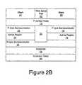
- Figures 2A and 2Billustrated operations according to some embodiments of the present invention for forming light emitting devices having an reduced conduction region as illustrated in Figure 1 .
- the various layers/regions of the light emitting deviceare fabricated. The particular operations in the fabrication of the light emitting device will depend on the structure to be fabricated and are described in the United States Patents and/or Applications cited above and/or are well known to those of skill in the art and, therefore, need not be repeated herein.
- Figure 2Aalso illustrates formation of a mask 40 having a window 42 corresponding to the region where the wire bond pad 22 is to be formed.
- An implantis performed using the mask 40 so as to implant atoms into the active region 14 in the region of the wire bond pad 22 so as to form the reduced conduction region 30 as seen in Figure 2B .
- Such an implantmay, for example, be a nitrogen implant.
- implant conditions of 60keV, 2 x 10 13 cm -3 N 2may produce a non-absorbing and insulating region in Mg doped GaN.
- the particular implant energy and/or atomsmay depend on the structure in which the reduced conduction region 30 is formed.
- the wire bond pad 22may be formed in the window 42.
- the wire bond pad 22 and the reduced conduction region 30are self-aligned.
- the wire bond pad 22may be formed, for example, by forming a layer or layers of the metal from which the wire bond pad 22 is formed and then planarizing the layers to provide the wire bond pad 22.
- the mask 40may subsequently be removed.
- the mask 40may be made of an insulating material, such as SiO 2 and/or AlN, and may remain on the device as, for example, a passivation layer, or be removed.
- bond padrefers to a light absorbing contact structure.
- a bond padmay be a single or multiple layers, may be a metal and/or metal alloy and/or may be of uniform or non-uniform composition.
- the reduced conduction region 30may be formed before or after forming the second contact metal layer 20 .
Landscapes
- Led Devices (AREA)
- Semiconductor Lasers (AREA)
- Luminescent Compositions (AREA)
- Control Of El Displays (AREA)
Abstract
Description
- This invention relates to semiconductor light emitting diodes and fabricating methods therefor.
- Semiconductor light emitting devices, such as Light Emitting Diodes (LEDs) or laser diodes, are widely used for many applications. As is well known to those having skill in the art, a semiconductor light emitting device includes a semiconductor light emitting element having one or more semiconductor layers that are configured to emit coherent and/or incoherent light upon energization thereof. As is well known to those having skill in the art, a light emitting diode or laser diode, generally includes a diode region on a microelectronic substrate. The microelectronic substrate may be, for example, gallium arsenide, gallium phosphide, alloys thereof, silicon carbide and/or sapphire. Continued developments in LEDs have resulted in highly efficient and mechanically robust light sources that can cover the visible spectrum and beyond. These attributes, coupled with the potentially long service life of solid state devices, may enable a variety of new display applications, and may place LEDs in a position to compete with the well entrenched incandescent and fluorescent lamps.
- Much development interest and commercial activity recently has focused on LEDs that are fabricated in or on silicon carbide, because these LEDs can emit radiation in the blue/green portions of the visible spectrum. See, for example,
U.S. Patent 5,416,342 to Edmond et al. , entitledBlue Light-Emirting Diode With High External Quantum Efficiency, assigned to the assignee of the present application. There also has been much interest in LEDs that include gallium nitride-based diode regions on silicon carbide substrates, because these devices also may emit light with high efficiency. See, for example,U.S. Patent 6,177,688 to Linthicum et al. . entitledPendeoepitaxial Gallium Nitride Semiconductor Layers On Silicon Carbide Substrates. - The efficiency of conventional LEDs may be limited by their inability to emit all of the light that is generated by their active region. When an LED is energized, light emitting from its active region (in all directions) may be prevented from exiting the LED by, for example, a light absorbing wire bond pad. Typically in gallium nitride based LEDs, a current spreading contact layer is provided to improve the uniformity of carrier injection across the cross section of the light emitting device. Current is injected into the p-side of the LED through the bond pad and the p-type contact. Light generated in an active region of the device is proportional to the carrier injection. Thus, substantially uniform photon emission across the active region may result from the use of a current spreading layer, such as a substantially transparent p-type contact layer. However, a wire bond pad is typically not a transparent structure and, therefore, photons emitted from the active region of the LED that are incident upon the wire bond pad may be absorbed by the wire bond pad. For example, in some instances approximately 70% of the light incident on the wire bond pad may be absorbed. Such photon absorption may reduce the amount of light that escapes from the LED and may decrease the efficiency of the LED.
- Lee et al, in an article entitled Characteristics of Top-Surface-Emitting GaAs Quantum-Well Lasers (IEEE Photonics Technology Letters, 2 No.9 September 1990) discloses self-aligned, top-surface-emitting, vertical-cavity, GaAs four-quantum-well lasers in which deep buried damaged layers formed by proton implantation are used to control vertical conductivity profiles for efficient current injection at the active region. The light output is through an output window formed in an Au/Zn electrode formed on the surface of the active region. Vertical damaged areas concentrate the current in the active region below the output window.
WO 03/061021 US-A-2004/0066820 discloses a single mode vertical cavity surface emitting laser (VCSEL) wherein a multi-quantum well active region is located between upper and lower mirrors, insulating layers being formed over the upper mirror, light from the active region being caused to pass through an aperture in the insulating layers, an equipotential layer above the insulating layers and dielectric layers on the surface of the laser. Upper electrical contacts are positioned on the surface of the equipotential layer, with isolation regions below them. VCSELs having similar current confinement structures formed by ion implantation are disclosed inWO 03/058772 A2 - Yoo et al (Japanese Journal of Applied Physics, 30, No. 3B, March 1991 pp. L492-L494) disclose front surface emitting laser diodes having both n and p electrodes on the top surface, laser light being emitted through a central aperture in the p electrode. The current flows bypassing high series resistance Distributed Bragg Reflector (DBR) stacks.
US-A-5245622 discloses vertical-cavity surface-emitting lasers wherein light from the active region passes through a stratified electrode comprising high and low doped layers and through a dielectric upper mirror on the surface of the stratified electrode. Electrical contacts are also positioned on the surface of the stratified electrodes, and blocking regions adjacent the active region are positioned below these contacts to confine the current, and hence the light emission, to a region below the upper mirror.- According to the present invention, there is provided a light emitting as defined in claim 1.
- In additional embodiments of the present invention the active region includes a Group III-nitride based active region. The insulating region may also be a region that is not light absorbing. The insulating regions may include an implanted region.
- Also in accordance with the present invention there is provided a method of fabricating a light emitting diode as defined in claim 7.
- Preferred embodiments of the invention will now be described with reference to the accompanying drawings wherein:
Figure 1 is a cross-sectional view illustrating semiconductor light emitting devices having a current blocking structure according to some embodiments of the present invention, andFigures 2A and2B are cross-sectional views illustrating fabrication of semiconductor devices according to some embodiments of the present invention.- In the drawings, the thickness of layers and regions are exaggerated for clarity. Like numbers refer to like elements throughout. As used herein the term "and/or" includes any and all combinations of one or more of the associated listed items.
- The terminology used herein is for the purpose of describing particular embodiments only and is not intended to be limiting of the invention. As used herein, the singular forms "a", "an" and "the" are intended to include the plural forms as well, unless the context clearly indicates otherwise. It will be further understood that the terms "comprises" and/or "comprising," when used in this specification, specify the presence of stated features, integers, steps, operations, elements, and/or components, but do not preclude the presence or addition of one or more other features, integers, steps, operations, elements, components, and/or groups thereof.
- It will be understood that when an element such as a layer, region or substrate is referred to as being "on" or extending "onto" another element, it can be directly on or extend directly onto the other element or intervening elements may also be present. In contrast, when an element is referred to as being "directly on" or extending "directly onto" another element, there are no intervening elements present. It will also be understood that when an element is referred to as being "connected" or "coupled" to another element, it can be directly connected or coupled to the other element or intervening elements may be present. In contrast, when an element is referred to as being "directly connected" or "directly coupled" to another element, there are no intervening elements present. Like numbers refer to like elements throughout the specification.
- It will be understood that, although the terms first, second, etc. may be used herein to describe various elements, components, regions, layers and/or sections, these elements, components, regions, layers and/or sections should not be limited by these terms. These terms are only used to distinguish one element, component, region, layer or section from another region, layer or section. Thus, a first element, component, region, layer or section discussed below could be termed a second element, component, region, layer or section without departing from the teachings of the present invention.
- Furthermore, relative terms, such as "lower" or "bottom" and "upper" or "top," may be used herein to describe one element's relationship to another elements as illustrated in the Figures. It will be understood that relative terms are intended to encompass different orientations of the device in addition to the orientation depicted in the Figures. For example, if the device in the Figures is turned over, elements described as being on the "lower" side of other elements would then be oriented on "upper" sides of the other elements. The exemplary term "lower", can therefore, encompasses both an orientation of "lower" and "upper," depending on the particular orientation of the figure. Similarly, if the device in one of the figures is turned over, elements described as "below" or "beneath" other elements would then be oriented "above" the other elements. The exemplary terms "below" or "beneath" can, therefore, encompass both an orientation of above and below.
- Embodiments of the present invention are described herein with reference to cross-section illustrations that are schematic illustrations of idealized embodiments of the present invention. As such, variations from the shapes of the illustrations as a result, for example, of manufacturing techniques and/or tolerances, are to be expected. Thus, embodiments of the present invention should not be construed as limited to the particular shapes of regions illustrated herein but are to include deviations in shapes that result, for example, from manufacturing. For example, an etched region illustrated or described as a rectangle will, typically, have rounded or curved features. Thus, the regions illustrated in the figures are schematic in nature and their shapes are not intended to illustrate the precise shape of a region of a device and are not intended to limit the scope of the present invention.
- Unless otherwise defined, all terms (including technical and scientific terms) used herein have the same meaning as commonly understood by one of ordinary skill in the art to which this invention belongs. It will be further understood that terms, such as those defined in commonly used dictionaries, should be interpreted as having a meaning that is consistent with their meaning in the context of the relevant art and will not be interpreted in an idealized or overly formal sense unless expressly so defined herein.
- It will also be appreciated by those of skill in the art that references to a structure or feature that is disposed "adjacent" another feature may have portions that overlap or underlie the adjacent feature.
- Although various embodiments of LEDs disclosed herein include a substrate, it will be understood by those skilled in the art that the crystalline epitaxial growth substrate on which the epitaxial layers comprising an LED are grown may be removed, and the freestanding epitaxial layers may be mounted on a substitute carrier substrate or submount which may have better thermal, electrical, structural and/or optical characteristics than the original substrate. The invention described herein is not limited to structures having crystallize epitaxial growth substrates and may be utilized in connection with structures in which the epitaxial layers have been removed from their original growth substrates and bonded to substitute carrier substrates.
- Some embodiments of the present invention may provide for improved efficacy of a light emitting device by reducing and/or preventing current flow in an active region of the device in a region beneath a wire bond pad or other light absorbing structure. Thus, some embodiments of the present invention may provide light emitting devices and methods of fabricating light emitting devices having a current blocking mechanism below the wire bond pad. By reducing and/or preventing current from being injected directly beneath the wire bond pad, the current may be more likely to be converted to photon emission in areas of the device not under the wire bond pad. Thus, there may be a reduced probability of light being absorbed by the wire bond pad. In some embodiments of the present invention, an increase in efficiency of a light emitting device according to some embodiments of the present invention may be proportional to the size of the wire bond pad.
- Embodiments of the present invention may be particularly well suited for use in nitride-based light emitting devices such as Group III-nitride based devices. As used herein, the term "Group III nitride" refers to those semiconducting compounds formed between nitrogen and the elements in Group III of the periodic table, usually aluminum (Al), gallium (Ga), and/or indium (In). The term also refers to ternary and quaternary compounds such as AlGaN and AlInGaN. As is well understood by those in this art, the Group III elements can combine with nitrogen to form binary (e.g., GaN), ternary (e.g., AlGaN, AlInN), and quaternary (e.g., AlInGaN) compounds. These compounds all have empirical formulas in which one mole of nitrogen is combined with a total of one mole of the Group III elements. Accordingly, formulas such as AlxGa1-xN where 0 ≤ x ≤ 1 are often used to describe them. However, while embodiments of the present invention are described herein with reference to Group III-nitride based light emitting devices, such as gallium nitride based light emitting devices, certain embodiments of the present invention may be suitable for use in other semiconductor light emitting devices, such as for example, GaAs and/or GaP based devices.
- Light emitting diodes according to some embodiments of the present invention include a light emitting diode which includes one or more semiconductor layers, which may include silicon, silicon carbide, gallium nitride and/or other semiconductor materials, a substrate which may include sapphire, silicon, silicon carbide and/or other microelectronic substrates, and one or more contact layers which may include metal and/or other conductive layers. In some embodiments, ultraviolet, blue and/or green LEDs may be provided. The design and fabrication of semiconductor light emitting devices are well known to those having skill in the art and need not be described in detail herein.
- For example, light emitting devices according to some embodiments of the present invention may include structures such as the gallium nitride-based LED and/or laser structures fabricated on a silicon carbide substrate such as those devices manufactured and sold by Cree, Inc. of Durham, North Carolina. The present invention may be suitable for use with LED and/or laser structures that provide active regions such as described in United States Patent Nos.
6,201,262 ;6,187,606 ;6,120,600 ;5,912,477 ;5,739,554 ;5,631,190 ;5,604,135 ;5,523,589 ;5,416,342 ;5,393,993 ;5,338,944 ;5,210,051 ;5,027,168 ;4,966,862 and/or4,918,497 . Other suitable LED and/or laser structures are described in published U.S. Patent Publication No.US 2003/0006418 A1 entitledGroup III Nitride Based Light Emitting Diode Structures With a Quantum Well and Superlattice, Group III Nitride Based Quantum Well Structures and Group III Nitride Based Superlattice Structures, published January 9, 2003, as well as published U.S. Patent Publication No.US 2002/0123164 A1 entitledLight Emitting Diodes Including Modifications for Light Extraction and Manufacturing Methods Therefor. Furthermore, phosphor coated LEDs, such as those described inU.S. Application Serial No. 10/659,241 US 2002/0123164 A1 . These structures may be modified as described herein to provide blocking structures according to some embodiments of the present invention. - Thus, for example, embodiments of the present invention may be utilized with light emitting devices having bond pads of differing shapes or sizes. The light emitting devices may be on differing substrates, such as silicon carbide, sapphire, gallium nitride, silicon or other substrate suitable for providing Group III-nitride devices. The light emitting devices may be suitable for subsequent singulation and mounting on a suitable carrier. The light emitting devices may include, for example, single quantum well, multi-quantum well and/or bulk active region devices. Some embodiments of the present invention may be used with devices utilizing a tunneling contact on the p-side of the device.
Figure 1 is a cross-sectional schematic illustration of a light emitting device according to some embodiments of the present invention. As seen inFigure 1 , asubstrate 10, such as an n-type silicon carbide substrate, has an optional n-type semiconductor layer 12, such as a gallium nitride based layer, provided thereon. The n-type semiconductor layer 12 may include multiple layers, for example, buffer layers or the like. In some embodiments of the present invention, the n-type semiconductor layer 12 is provided as a silicon doped AlGaN layer, that may be of uniform or gradient composition, and a silicon doped GaN layer.- While described herein with reference to a silicon carbide substrate, in some embodiments of the present invention other substrate materials may be utilized. For example, a sapphire substrate, GaN or other substrate material may be utilized. In such a case, the
contact 20 may be located, for example, in a recess that contacts the n-type semiconductor layer 12, so as to provide a second contact for the device. Other configurations may also be utilized. - An
active region 14, such as a single or double heterostructure, quantum well, multi-quantum well or other such active region may be provided on the n-type semiconductor layer. As used herein, the term "active region" refers to a region of semiconductor material of a light emitting device, that may be one or more layers and/or portions thereof, where a substantial portion of the photons emitted by the device when in operation are generated by carrier recombination. In the present invention, the active region refers to a region where substantially all of the photons emitted by the device are generated by carrier recombination. - Also illustrated in
Figure 1 is a p-type semiconductor layer 16. The p-ypesemiconductor material layer 16 may, for example, be a gallium nitride based layer, such as a GaN layer. In particular embodiments of the present invention, the p-type semiconductor layer 16 includes magnesium doped GaN. The p-type semiconductor layer 16 may include one or multiple layers and may be of uniform or gradient composition. - A first
contact metal layer 18 of contact metal that provides an ohmic contact to the p-typesemiconductor material layer 16 is also provided. In some embodiments, the firstcontact metal layer 18 may function as a current spreading layer. In particular embodiments of the present invention where the p-typesemiconductor material layer 16 is GaN, the firstcontact metal layer 18 may be Pt. The firstcontact metal layer 18 is light permeable and in some embodiments is substantially transparent. In some embodiments, the firstcontact metal layer 18 may be a relatively thin layer of Pt. For example, the firstcontact metal layer 18 may be a layer of Pt that is about 54 Å thick. A light-absorbingwire bond pad 22 is provided on the firstcontact metal layer 18. - A second
contact metal layer 20 of contact metal that provides an ohmic contact to the n-type semiconductor material is also provided. The secondcontact metal layer 20 may be provided on a side of thesubstrate 10 opposite theactive region 14. As discussed above, in some embodiments of the present invention the second contact metal layer may be provided on a portion of the n-typesemiconductor material layer 12, for example, in a recess or at a base of a mesa including the active region. Furthermore, in some embodiments of the present invention, an optional back-side implant or additional epitaxial layers may be provide between thesubstrate 10 and the secondcontact metal layer 20. - As is further illustrated in
Figure 1 , a reducedconduction region 30 is provided in theactive region 14 and is positioned beneath thewire bond pad 22. In some embodiments of the present invention, the reducedconduction region 30 extends through theactive region 14. As used herein, "reduced conduction region" refers to a region with reduced current flow over other portions of the active region. In particular embodiments, the reduction is at least an order of magnitude and in some embodiments, substantially all current flow is blocked in the reduced conduction region. In some embodiments of the present invention the reducedconduction region 30 extends through theactive region 14. In the present invention, the reduced conduction region extends from thefirst contact layer 18 into theactive region 14. In some embodiments, the reduced conduction region extends from thefirst contact layer 18 through theactive region 14. The reducedconduction region 30 has substantially the same shape and/area as the area of thewire bond pad 22 on the firstcontact metal layer 18. In other examples not forming part of the present invention, the reducedconduction region 30 has a slightly larger area than thewire bond pad 22 while in said other examples not forming part of the present invention, the reducedconduction region 30 has a slightly smaller area than thewire bond pad 22. In certain embodiments of the present invention, the reducedconduction region 30 does not absorb light or only absorbs a relatively small amount of light. In the present invention, the reducedconduction region 30 is an insulating region. - The reduced
conduction region 30 may reduce and/or prevent current flow through theactive region 14 in the area beneath thewire bond pad 22 and, therefore, may reduce and/or prevent light generation through carrier recombination in this region. While not being bound by a particular theory of operation, this may be the case because the likelihood that a photon generated in the portion of the active region beneath thewire bond pad 22 is absorbed by thewire bond pad 22 may be higher than if the photon is generated in a portion of the active region that is not beneath thewire bond pad 22. By reducing and/or eliminating the light generated in the active region beneath thewire bond pad 22, the portion of the light generated by the light emitting device that is absorbed by thewire bond pad 22 may be reduced. For a given set of operating conditions, this reduction in the amount of light absorbed by thewire bond pad 22 may result in increased light extraction from the light emitting device as compared to a device operating under the same conditions where light is generated in the region beneath thewire bond pad 22. Thus, some embodiments of the present invention provide a reducedconduction region 30 that extends into and, in some embodiments, through theactive region 14 in the area beneath thewire bond pad 22. This may reduce the likelihood that carriers may spread and be injected into theactive region 14 beneath thewire bond pad 22 and, thereby, result in photon generation in the area beneath thewire bond pad 22. Figures 2A and2B illustrated operations according to some embodiments of the present invention for forming light emitting devices having an reduced conduction region as illustrated inFigure 1 . As seen inFigure 2A , the various layers/regions of the light emitting device are fabricated. The particular operations in the fabrication of the light emitting device will depend on the structure to be fabricated and are described in the United States Patents and/or Applications cited above and/or are well known to those of skill in the art and, therefore, need not be repeated herein.Figure 2A also illustrates formation of amask 40 having awindow 42 corresponding to the region where thewire bond pad 22 is to be formed.- An implant is performed using the
mask 40 so as to implant atoms into theactive region 14 in the region of thewire bond pad 22 so as to form the reducedconduction region 30 as seen inFigure 2B . Such an implant may, for example, be a nitrogen implant. For example, for a gallium nitride based device, implant conditions of 60keV, 2 x 1013 cm-3 N2 may produce a non-absorbing and insulating region in Mg doped GaN. The particular implant energy and/or atoms may depend on the structure in which the reducedconduction region 30 is formed. - As seen in
Figure 2B , after implantation, thewire bond pad 22 may be formed in thewindow 42. Thus, in the present invention, thewire bond pad 22 and the reducedconduction region 30 are self-aligned. Thewire bond pad 22 may be formed, for example, by forming a layer or layers of the metal from which thewire bond pad 22 is formed and then planarizing the layers to provide thewire bond pad 22. Themask 40 may subsequently be removed. Optionally, themask 40 may be made of an insulating material, such as SiO2 and/or AlN, and may remain on the device as, for example, a passivation layer, or be removed. - While embodiments of the present invention are illustrated in
Figures 1 ,2A and2B with reference to particular light emitting device structures, other structures may be provided according to some embodiments of the present invention. Thus, embodiments of the present invention may be provided by any light emitting structure as defined in the independent claims. For example, current blocking mechanisms according to some embodiments of the present invention may be provided in conjunction with the exemplary light emitting device structures discussed in the United States Patents and/or Applications cited above. - Embodiments of the present invention have been described with reference to a
wire bond pad 22. As used herein, the term bond pad refers to a light absorbing contact structure. A bond pad may be a single or multiple layers, may be a metal and/or metal alloy and/or may be of uniform or non-uniform composition. - Furthermore, while embodiments of the present invention have been described with reference to a particular sequence of operations, variations from the described sequence may be provided while still benefiting from the teachings of the present invention. Thus, two or more steps may be combined into a single step or steps performed out of the sequence described herein. For example, the reduced
conduction region 30 may be formed before or after forming the secondcontact metal layer 20.
Claims (11)
- A light emitting diode, comprising:an active region (14) of semiconductor material in which the photons emitted by the device are generated, a first contact on the active region, including a light absorbing bond pad (22);a p-type semiconductor material (16) disposed between the first contact and the active region (14);an insulating region (30) disposed in the active region beneath the bond pad of the first contact and configured to reduce current flow through the active region in the region beneath the bond pad region of the first contact; anda second contact (20) electrically coupled to the active region;wherein the bond pad is formed on a bond pad region of the first contact, the bond pad and the insulating region being aligned with with each other and the insulating region having substantially the same shape, and approximately the same area, as the surface covered by the bond pad,
characterised in that the first contact comprises a light permeable metal layer (18) andin that the insulating region (30) extends from the light permeable metal layer (18) through the p-type semiconductor material into the active region (14). - A light emitting diode according to claim 1, wherein the insulating region (30) extends from the light permeable metal layer (18) through the active region (14).
- A light emitting diode according to any preceding claim, wherein the active region (14) comprises a Group III-nitride based active region.
- A light emitting diode according to any preceding claim, wherein the light permeable metal layer (18) is a layer of platinum.
- A light emitting diode according to any preceding claim, wherein the insulating region (30) comprises a region that is not light absorbing.
- A light emitting diode according to any preceding claim, wherein the insulating region (30) comprises an implanted region.
- A method of fabricating a light emitting diode according to any preceding claim, comprising:forming an active region (14) of semiconductor material;forming a layer of p-type semiconductor material (16) on the active region;forming a first contact comprising a light permeable metal layer (18) on the p-type semiconductor material and forming a light absorbing bond pad (22) on said light permeable metal layer;forming an insulating region (30) in the active region beneath the bond pad, aligned with the bond pad and having substantially the same shape, and approximately the same area, as the surface covered by the bond pad, extending from the first contact (18) into the active region (14), and configured to block current flow through the active region in the region beneath the bond pad; andforming a second contact (20) electrically coupled to the active region.
- A method according to claim 7, wherein the insulating region (30) is formed to extend through the active region (14).
- A method according to claim 7 or claim 8, wherein the active region comprises a Group III-nitride based active region.
- A method according to any of claims 7 to 9, wherein the light permeable metal layer (18) is a layer of platinum.
- A method according to any of claims 7 to 10, wherein the step forming an insulating region (30) comprises:forming a mask layer (40) on the light permeable metal layer (18), the mask layer having an opening (42) corresponding to the bond pad region;implanting atoms in the active region (14) through the opening in the mask layer; andforming the bond pad (22) in the opening (42) in the mask layer (40).
Applications Claiming Priority (2)
| Application Number | Priority Date | Filing Date | Title |
|---|---|---|---|
| US10/881,814US20060002442A1 (en) | 2004-06-30 | 2004-06-30 | Light emitting devices having current blocking structures and methods of fabricating light emitting devices having current blocking structures |
| PCT/US2005/010868WO2006011936A2 (en) | 2004-06-30 | 2005-03-30 | Light emitting devices having current blocking structures and methods of fabricating light emitting devices having current blocking structures |
Publications (2)
| Publication Number | Publication Date |
|---|---|
| EP1766697A2 EP1766697A2 (en) | 2007-03-28 |
| EP1766697B1true EP1766697B1 (en) | 2010-02-24 |
Family
ID=35513875
Family Applications (1)
| Application Number | Title | Priority Date | Filing Date |
|---|---|---|---|
| EP05763653AExpired - LifetimeEP1766697B1 (en) | 2004-06-30 | 2005-03-30 | Light emitting devices having current blocking structures and methods of fabricating light emitting devices having current blocking structures |
Country Status (11)
| Country | Link |
|---|---|
| US (2) | US20060002442A1 (en) |
| EP (1) | EP1766697B1 (en) |
| JP (3) | JP4904261B2 (en) |
| KR (2) | KR101418190B1 (en) |
| CN (2) | CN1977398A (en) |
| AT (1) | ATE459106T1 (en) |
| CA (1) | CA2567794A1 (en) |
| DE (1) | DE602005019569D1 (en) |
| MY (1) | MY143633A (en) |
| TW (2) | TWI451589B (en) |
| WO (1) | WO2006011936A2 (en) |
Families Citing this family (73)
| Publication number | Priority date | Publication date | Assignee | Title |
|---|---|---|---|---|
| US6958497B2 (en)* | 2001-05-30 | 2005-10-25 | Cree, Inc. | Group III nitride based light emitting diode structures with a quantum well and superlattice, group III nitride based quantum well structures and group III nitride based superlattice structures |
| EP1756875A4 (en)* | 2004-04-07 | 2010-12-29 | Tinggi Technologies Private Ltd | FABRICATION OF A RETROFLECTIVE LAYER ON SEMICONDUCTOR ELECTROLUMINESCENT DIODES |
| US7795623B2 (en)* | 2004-06-30 | 2010-09-14 | Cree, Inc. | Light emitting devices having current reducing structures and methods of forming light emitting devices having current reducing structures |
| US20060002442A1 (en)* | 2004-06-30 | 2006-01-05 | Kevin Haberern | Light emitting devices having current blocking structures and methods of fabricating light emitting devices having current blocking structures |
| TWI352437B (en) | 2007-08-27 | 2011-11-11 | Epistar Corp | Optoelectronic semiconductor device |
| US7335920B2 (en) | 2005-01-24 | 2008-02-26 | Cree, Inc. | LED with current confinement structure and surface roughening |
| US8097897B2 (en)* | 2005-06-21 | 2012-01-17 | Epistar Corporation | High-efficiency light-emitting device and manufacturing method thereof |
| SG133432A1 (en) | 2005-12-20 | 2007-07-30 | Tinggi Tech Private Ltd | Localized annealing during semiconductor device fabrication |
| KR100723150B1 (en)* | 2005-12-26 | 2007-05-30 | 삼성전기주식회사 | Vertical nitride semiconductor light emitting device and manufacturing method |
| SG140473A1 (en) | 2006-08-16 | 2008-03-28 | Tinggi Tech Private Ltd | Improvements in external light efficiency of light emitting diodes |
| KR100867529B1 (en)* | 2006-11-14 | 2008-11-10 | 삼성전기주식회사 | Vertical light emitting device |
| US9178121B2 (en)* | 2006-12-15 | 2015-11-03 | Cree, Inc. | Reflective mounting substrates for light emitting diodes |
| DE102007008524A1 (en)* | 2007-02-21 | 2008-08-28 | Osram Opto Semiconductors Gmbh | Radiation emitting chip with at least one semiconductor body |
| US7847312B2 (en)* | 2007-09-14 | 2010-12-07 | Sharp Kabushiki Kaisha | Nitride semiconductor light-emitting device |
| JP5178360B2 (en)* | 2007-09-14 | 2013-04-10 | シャープ株式会社 | Nitride semiconductor light emitting device |
| US8536584B2 (en)* | 2007-11-14 | 2013-09-17 | Cree, Inc. | High voltage wire bond free LEDS |
| US8368100B2 (en) | 2007-11-14 | 2013-02-05 | Cree, Inc. | Semiconductor light emitting diodes having reflective structures and methods of fabricating same |
| US8575633B2 (en)* | 2008-12-08 | 2013-11-05 | Cree, Inc. | Light emitting diode with improved light extraction |
| US9634191B2 (en)* | 2007-11-14 | 2017-04-25 | Cree, Inc. | Wire bond free wafer level LED |
| CN103219415B (en)* | 2007-12-28 | 2016-09-28 | 晶元光电股份有限公司 | Optoelectronic semiconductor device and manufacturing method thereof |
| JP5126884B2 (en)* | 2008-01-16 | 2013-01-23 | シャープ株式会社 | Nitride semiconductor light emitting device and method for manufacturing nitride semiconductor light emitting device |
| EP2280426B1 (en)* | 2008-04-16 | 2017-07-05 | LG Innotek Co., Ltd. | Light-emitting device |
| US8664747B2 (en) | 2008-04-28 | 2014-03-04 | Toshiba Techno Center Inc. | Trenched substrate for crystal growth and wafer bonding |
| US7989834B2 (en)* | 2008-04-30 | 2011-08-02 | Lg Innotek Co., Ltd. | Light emitting device and method for manufacturing the same |
| US8384115B2 (en)* | 2008-08-01 | 2013-02-26 | Cree, Inc. | Bond pad design for enhancing light extraction from LED chips |
| KR101018227B1 (en)* | 2008-10-09 | 2011-02-28 | 삼성엘이디 주식회사 | Vertical structure nitride-based light emitting diode device and manufacturing method thereof |
| KR100992728B1 (en)* | 2008-10-20 | 2010-11-05 | 엘지이노텍 주식회사 | Light emitting device and manufacturing method |
| JP2010140936A (en)* | 2008-12-09 | 2010-06-24 | Sanyo Electric Co Ltd | Photovoltaic device and manufacturing method thereof |
| US8741715B2 (en)* | 2009-04-29 | 2014-06-03 | Cree, Inc. | Gate electrodes for millimeter-wave operation and methods of fabrication |
| JP2010263085A (en)* | 2009-05-07 | 2010-11-18 | Toshiba Corp | Light emitting element |
| US8207547B2 (en) | 2009-06-10 | 2012-06-26 | Brudgelux, Inc. | Thin-film LED with P and N contacts electrically isolated from the substrate |
| US8525221B2 (en) | 2009-11-25 | 2013-09-03 | Toshiba Techno Center, Inc. | LED with improved injection efficiency |
| TWI398965B (en)* | 2009-11-25 | 2013-06-11 | Formosa Epitaxy Inc | Light emitting diode chip and package structure thereof |
| US8604461B2 (en)* | 2009-12-16 | 2013-12-10 | Cree, Inc. | Semiconductor device structures with modulated doping and related methods |
| US8536615B1 (en) | 2009-12-16 | 2013-09-17 | Cree, Inc. | Semiconductor device structures with modulated and delta doping and related methods |
| US8575592B2 (en)* | 2010-02-03 | 2013-11-05 | Cree, Inc. | Group III nitride based light emitting diode structures with multiple quantum well structures having varying well thicknesses |
| KR101039609B1 (en)* | 2010-05-24 | 2011-06-09 | 엘지이노텍 주식회사 | Light emitting device, manufacturing method and light emitting device package |
| US9287452B2 (en) | 2010-08-09 | 2016-03-15 | Micron Technology, Inc. | Solid state lighting devices with dielectric insulation and methods of manufacturing |
| US8502244B2 (en) | 2010-08-31 | 2013-08-06 | Micron Technology, Inc. | Solid state lighting devices with current routing and associated methods of manufacturing |
| US9070851B2 (en) | 2010-09-24 | 2015-06-30 | Seoul Semiconductor Co., Ltd. | Wafer-level light emitting diode package and method of fabricating the same |
| US8455882B2 (en) | 2010-10-15 | 2013-06-04 | Cree, Inc. | High efficiency LEDs |
| TW201236197A (en)* | 2011-02-23 | 2012-09-01 | Genesis Photonics Inc | Light emitting diode structure |
| US8395165B2 (en) | 2011-07-08 | 2013-03-12 | Bridelux, Inc. | Laterally contacted blue LED with superlattice current spreading layer |
| US20130026480A1 (en) | 2011-07-25 | 2013-01-31 | Bridgelux, Inc. | Nucleation of Aluminum Nitride on a Silicon Substrate Using an Ammonia Preflow |
| US8916906B2 (en) | 2011-07-29 | 2014-12-23 | Kabushiki Kaisha Toshiba | Boron-containing buffer layer for growing gallium nitride on silicon |
| US9343641B2 (en) | 2011-08-02 | 2016-05-17 | Manutius Ip, Inc. | Non-reactive barrier metal for eutectic bonding process |
| US9012939B2 (en) | 2011-08-02 | 2015-04-21 | Kabushiki Kaisha Toshiba | N-type gallium-nitride layer having multiple conductive intervening layers |
| US8865565B2 (en) | 2011-08-02 | 2014-10-21 | Kabushiki Kaisha Toshiba | LED having a low defect N-type layer that has grown on a silicon substrate |
| US9142743B2 (en) | 2011-08-02 | 2015-09-22 | Kabushiki Kaisha Toshiba | High temperature gold-free wafer bonding for light emitting diodes |
| US20130032810A1 (en) | 2011-08-03 | 2013-02-07 | Bridgelux, Inc. | Led on silicon substrate using zinc-sulfide as buffer layer |
| US8564010B2 (en) | 2011-08-04 | 2013-10-22 | Toshiba Techno Center Inc. | Distributed current blocking structures for light emitting diodes |
| JP6077201B2 (en) | 2011-08-11 | 2017-02-08 | 昭和電工株式会社 | Light emitting diode and manufacturing method thereof |
| US8624482B2 (en) | 2011-09-01 | 2014-01-07 | Toshiba Techno Center Inc. | Distributed bragg reflector for reflecting light of multiple wavelengths from an LED |
| US8669585B1 (en) | 2011-09-03 | 2014-03-11 | Toshiba Techno Center Inc. | LED that has bounding silicon-doped regions on either side of a strain release layer |
| US8558247B2 (en) | 2011-09-06 | 2013-10-15 | Toshiba Techno Center Inc. | GaN LEDs with improved area and method for making the same |
| US8686430B2 (en) | 2011-09-07 | 2014-04-01 | Toshiba Techno Center Inc. | Buffer layer for GaN-on-Si LED |
| US8853668B2 (en) | 2011-09-29 | 2014-10-07 | Kabushiki Kaisha Toshiba | Light emitting regions for use with light emitting devices |
| US9178114B2 (en) | 2011-09-29 | 2015-11-03 | Manutius Ip, Inc. | P-type doping layers for use with light emitting devices |
| US20130082274A1 (en) | 2011-09-29 | 2013-04-04 | Bridgelux, Inc. | Light emitting devices having dislocation density maintaining buffer layers |
| US8664679B2 (en) | 2011-09-29 | 2014-03-04 | Toshiba Techno Center Inc. | Light emitting devices having light coupling layers with recessed electrodes |
| US9012921B2 (en) | 2011-09-29 | 2015-04-21 | Kabushiki Kaisha Toshiba | Light emitting devices having light coupling layers |
| US8698163B2 (en) | 2011-09-29 | 2014-04-15 | Toshiba Techno Center Inc. | P-type doping layers for use with light emitting devices |
| JP2014532993A (en)* | 2011-11-07 | 2014-12-08 | コーニンクレッカ フィリップス エヌ ヴェ | Improved p-type contact with more uniform injection and less optical loss |
| US8581267B2 (en) | 2011-11-09 | 2013-11-12 | Toshiba Techno Center Inc. | Series connected segmented LED |
| US8552465B2 (en) | 2011-11-09 | 2013-10-08 | Toshiba Techno Center Inc. | Method for reducing stress in epitaxial growth |
| GB201402508D0 (en) | 2014-02-13 | 2014-04-02 | Mled Ltd | Semiconductor modification process and structures |
| USD826871S1 (en) | 2014-12-11 | 2018-08-28 | Cree, Inc. | Light emitting diode device |
| CN205944139U (en) | 2016-03-30 | 2017-02-08 | 首尔伟傲世有限公司 | Ultraviolet ray light -emitting diode spare and contain this emitting diode module |
| DE102017108435A1 (en)* | 2017-04-20 | 2018-10-25 | Osram Opto Semiconductors Gmbh | Semiconductor laser diode and method for producing a semiconductor laser diode |
| US11264539B2 (en) | 2018-12-03 | 2022-03-01 | Nanosys, Inc. | Light emitting diodes containing deactivated regions and methods of making the same |
| JP7424038B2 (en) | 2019-12-23 | 2024-01-30 | セイコーエプソン株式会社 | Light emitting device and projector |
| WO2023285875A1 (en)* | 2021-07-14 | 2023-01-19 | King Abdullah University Of Science And Technology | Iii-nitride-based light emitting device with a passivated layer and a method for manufacturing thereof |
| CN116505370B (en)* | 2023-06-20 | 2023-10-13 | 深圳市柠檬光子科技有限公司 | Edge-emitting laser and method of manufacturing the same |
Family Cites Families (69)
| Publication number | Priority date | Publication date | Assignee | Title |
|---|---|---|---|---|
| US533844A (en)* | 1895-02-05 | Ments | ||
| US4864370A (en)* | 1987-11-16 | 1989-09-05 | Motorola, Inc. | Electrical contact for an LED |
| EP0352221B1 (en)* | 1988-06-14 | 1994-03-09 | Ciba-Geigy Ag | Process for photochemically stabilising dyed or non dyed polypropylene fibres |
| US5027168A (en)* | 1988-12-14 | 1991-06-25 | Cree Research, Inc. | Blue light emitting diode formed in silicon carbide |
| US4918497A (en)* | 1988-12-14 | 1990-04-17 | Cree Research, Inc. | Blue light emitting diode formed in silicon carbide |
| US5048035A (en)* | 1989-05-31 | 1991-09-10 | Kabushiki Kaisha Toshiba | Semiconductor light emitting device |
| US4966862A (en)* | 1989-08-28 | 1990-10-30 | Cree Research, Inc. | Method of production of light emitting diodes |
| US5210051A (en)* | 1990-03-27 | 1993-05-11 | Cree Research, Inc. | High efficiency light emitting diodes from bipolar gallium nitride |
| US5245622A (en)* | 1992-05-07 | 1993-09-14 | Bandgap Technology Corporation | Vertical-cavity surface-emitting lasers with intra-cavity structures |
| JP3323324B2 (en)* | 1993-06-18 | 2002-09-09 | 株式会社リコー | Light emitting diode and light emitting diode array |
| US5416342A (en)* | 1993-06-23 | 1995-05-16 | Cree Research, Inc. | Blue light-emitting diode with high external quantum efficiency |
| JPH0794778A (en)* | 1993-09-22 | 1995-04-07 | Olympus Optical Co Ltd | Light emitting device |
| US5338944A (en)* | 1993-09-22 | 1994-08-16 | Cree Research, Inc. | Blue light-emitting diode with degenerate junction structure |
| US5393993A (en)* | 1993-12-13 | 1995-02-28 | Cree Research, Inc. | Buffer structure between silicon carbide and gallium nitride and resulting semiconductor devices |
| US5604135A (en)* | 1994-08-12 | 1997-02-18 | Cree Research, Inc. | Method of forming green light emitting diode in silicon carbide |
| US5523589A (en)* | 1994-09-20 | 1996-06-04 | Cree Research, Inc. | Vertical geometry light emitting diode with group III nitride active layer and extended lifetime |
| US5631190A (en)* | 1994-10-07 | 1997-05-20 | Cree Research, Inc. | Method for producing high efficiency light-emitting diodes and resulting diode structures |
| JPH08222797A (en)* | 1995-01-17 | 1996-08-30 | Hewlett Packard Co <Hp> | Semiconductor device and manufacturing method thereof |
| JPH08250768A (en)* | 1995-03-13 | 1996-09-27 | Toyoda Gosei Co Ltd | Semiconductor optical device |
| US5739554A (en)* | 1995-05-08 | 1998-04-14 | Cree Research, Inc. | Double heterojunction light emitting diode with gallium nitride active layer |
| DE19629920B4 (en)* | 1995-08-10 | 2006-02-02 | LumiLeds Lighting, U.S., LLC, San Jose | Light-emitting diode with a non-absorbing distributed Bragg reflector |
| JP3916011B2 (en)* | 1997-02-21 | 2007-05-16 | シャープ株式会社 | Gallium nitride compound semiconductor light emitting device and method for manufacturing the same |
| US6057562A (en)* | 1997-04-18 | 2000-05-02 | Epistar Corp. | High efficiency light emitting diode with distributed Bragg reflector |
| JP3912845B2 (en)* | 1997-04-24 | 2007-05-09 | シャープ株式会社 | Gallium nitride compound semiconductor light emitting diode and method for manufacturing the same |
| US5789768A (en)* | 1997-06-23 | 1998-08-04 | Epistar Corporation | Light emitting diode having transparent conductive oxide formed on the contact layer |
| JP3693468B2 (en)* | 1997-07-23 | 2005-09-07 | シャープ株式会社 | Semiconductor light emitting device |
| US6201262B1 (en)* | 1997-10-07 | 2001-03-13 | Cree, Inc. | Group III nitride photonic devices on silicon carbide substrates with conductive buffer interlay structure |
| JPH11135834A (en)* | 1997-10-27 | 1999-05-21 | Matsushita Electric Ind Co Ltd | Light emitting diode device and method of manufacturing the same |
| JP3741528B2 (en)* | 1997-12-15 | 2006-02-01 | シャープ株式会社 | Method for manufacturing gallium nitride based semiconductor device |
| JP3516434B2 (en)* | 1997-12-25 | 2004-04-05 | 昭和電工株式会社 | Compound semiconductor light emitting device |
| JPH11204833A (en)* | 1998-01-08 | 1999-07-30 | Pioneer Electron Corp | Method for manufacturing semiconductor light emitting device |
| JP3653384B2 (en)* | 1998-02-10 | 2005-05-25 | シャープ株式会社 | Manufacturing method of light emitting diode |
| US6177688B1 (en)* | 1998-11-24 | 2001-01-23 | North Carolina State University | Pendeoepitaxial gallium nitride semiconductor layers on silcon carbide substrates |
| US6376269B1 (en)* | 1999-02-02 | 2002-04-23 | Agilent Technologies, Inc. | Vertical cavity surface emitting laser (VCSEL) using buried Bragg reflectors and method for producing same |
| JP4382912B2 (en)* | 1999-08-26 | 2009-12-16 | 昭和電工株式会社 | AlGaInP light emitting diode |
| JP2001077414A (en)* | 1999-09-07 | 2001-03-23 | Showa Denko Kk | Group iii nitride semiconductor light-emitting diode |
| JP2001111103A (en)* | 1999-10-14 | 2001-04-20 | Korai Kagi Kofun Yugenkoshi | Region current density controllable led |
| JP2001274456A (en)* | 2000-01-18 | 2001-10-05 | Sharp Corp | Light emitting diode |
| US6455343B1 (en)* | 2000-03-28 | 2002-09-24 | United Epitaxy Company, Ltd. | Method of manufacturing light emitting diode with current blocking structure |
| JP3975388B2 (en)* | 2000-04-07 | 2007-09-12 | サンケン電気株式会社 | Semiconductor light emitting device |
| US6420732B1 (en)* | 2000-06-26 | 2002-07-16 | Luxnet Corporation | Light emitting diode of improved current blocking and light extraction structure |
| JP2002026386A (en)* | 2000-07-10 | 2002-01-25 | Toyoda Gosei Co Ltd | Group III nitride compound semiconductor light emitting device |
| TW461124B (en)* | 2000-11-14 | 2001-10-21 | Advanced Epitaxy Technology In | Light emitting diode device with high light transmittance |
| US6905900B1 (en) | 2000-11-28 | 2005-06-14 | Finisar Corporation | Versatile method and system for single mode VCSELs |
| US6791119B2 (en)* | 2001-02-01 | 2004-09-14 | Cree, Inc. | Light emitting diodes including modifications for light extraction |
| US6468824B2 (en)* | 2001-03-22 | 2002-10-22 | Uni Light Technology Inc. | Method for forming a semiconductor device having a metallic substrate |
| JP2002329885A (en)* | 2001-05-01 | 2002-11-15 | Rohm Co Ltd | Semiconductor light emitting device |
| US6958497B2 (en)* | 2001-05-30 | 2005-10-25 | Cree, Inc. | Group III nitride based light emitting diode structures with a quantum well and superlattice, group III nitride based quantum well structures and group III nitride based superlattice structures |
| JP2003008055A (en)* | 2001-06-20 | 2003-01-10 | Daido Steel Co Ltd | Method for manufacturing semiconductor light emitting device |
| JP2003017748A (en)* | 2001-06-27 | 2003-01-17 | Seiwa Electric Mfg Co Ltd | Gallium nitride-based compound semiconductor light emitting element and manufacturing method therefor |
| JP4058590B2 (en)* | 2001-06-29 | 2008-03-12 | サンケン電気株式会社 | Semiconductor light emitting device |
| US6740906B2 (en)* | 2001-07-23 | 2004-05-25 | Cree, Inc. | Light emitting diodes including modifications for submount bonding |
| JP4089194B2 (en)* | 2001-09-28 | 2008-05-28 | 日亜化学工業株式会社 | Nitride semiconductor light emitting diode |
| TWI276230B (en)* | 2001-12-04 | 2007-03-11 | Epitech Corp Ltd | Structure and manufacturing method of light emitting diode |
| US20030180980A1 (en)* | 2001-12-21 | 2003-09-25 | Tal Margalith | Implantation for current confinement in nitride-based vertical optoelectronics |
| TW513820B (en)* | 2001-12-26 | 2002-12-11 | United Epitaxy Co Ltd | Light emitting diode and its manufacturing method |
| US6738409B2 (en) | 2001-12-28 | 2004-05-18 | Honeywell International Inc. | Current confinement, capacitance reduction and isolation of VCSELs using deep elemental traps |
| TW513821B (en)* | 2002-02-01 | 2002-12-11 | Hsiu-Hen Chang | Electrode structure of LED and manufacturing the same |
| US6919585B2 (en)* | 2002-05-17 | 2005-07-19 | Lumei Optoelectronics, Inc. | Light-emitting diode with silicon carbide substrate |
| KR101182041B1 (en)* | 2002-09-19 | 2012-09-11 | 크리 인코포레이티드 | Phosphor-coated light emitting diodes including tapered sidewalls, and fabrication methods therefor |
| JP2004165436A (en)* | 2002-11-13 | 2004-06-10 | Rohm Co Ltd | Method of manufacturing semiconductor light emitting device |
| JP2004172189A (en)* | 2002-11-18 | 2004-06-17 | Shiro Sakai | Nitride semiconductor device and its manufacturing method |
| JP3720341B2 (en)* | 2003-02-12 | 2005-11-24 | ローム株式会社 | Semiconductor light emitting device |
| JP4191566B2 (en)* | 2003-09-12 | 2008-12-03 | アトミック エナジー カウンセル − インスティトゥート オブ ニュークリアー エナジー リサーチ | LIGHT EMITTING DIODE HAVING CURRENT BLOCK STRUCTURE AND METHOD FOR MANUFACTURING THE SAME |
| US7009214B2 (en)* | 2003-10-17 | 2006-03-07 | Atomic Energy Council —Institute of Nuclear Energy Research | Light-emitting device with a current blocking structure and method for making the same |
| JP2004096130A (en)* | 2003-12-01 | 2004-03-25 | Showa Denko Kk | Nitride semiconductor light emitting diode |
| US20060002442A1 (en)* | 2004-06-30 | 2006-01-05 | Kevin Haberern | Light emitting devices having current blocking structures and methods of fabricating light emitting devices having current blocking structures |
| JP2006066518A (en)* | 2004-08-25 | 2006-03-09 | Sharp Corp | Semiconductor light emitting device and method for manufacturing semiconductor light emitting device |
| US7335920B2 (en)* | 2005-01-24 | 2008-02-26 | Cree, Inc. | LED with current confinement structure and surface roughening |
- 2004
- 2004-06-30USUS10/881,814patent/US20060002442A1/ennot_activeAbandoned
- 2005
- 2005-03-30CNCNA2005800220829Apatent/CN1977398A/enactivePending
- 2005-03-30EPEP05763653Apatent/EP1766697B1/ennot_activeExpired - Lifetime
- 2005-03-30KRKR1020127014255Apatent/KR101418190B1/ennot_activeExpired - Lifetime
- 2005-03-30CACA002567794Apatent/CA2567794A1/ennot_activeAbandoned
- 2005-03-30DEDE602005019569Tpatent/DE602005019569D1/ennot_activeExpired - Lifetime
- 2005-03-30CNCN200910224555Apatent/CN101714606A/enactivePending
- 2005-03-30JPJP2007519194Apatent/JP4904261B2/ennot_activeExpired - Lifetime
- 2005-03-30KRKR1020137007789Apatent/KR101418224B1/ennot_activeExpired - Lifetime
- 2005-03-30ATAT05763653Tpatent/ATE459106T1/ennot_activeIP Right Cessation
- 2005-03-30WOPCT/US2005/010868patent/WO2006011936A2/ennot_activeApplication Discontinuation
- 2005-04-14MYMYPI20051656Apatent/MY143633A/enunknown
- 2005-04-19TWTW094112476Apatent/TWI451589B/ennot_activeIP Right Cessation
- 2005-04-19TWTW102119636Apatent/TWI506811B/ennot_activeIP Right Cessation
- 2007
- 2007-03-02USUS11/681,410patent/US20070145392A1/ennot_activeAbandoned
- 2008
- 2008-03-12JPJP2008062736Apatent/JP5009841B2/ennot_activeExpired - Lifetime
- 2011
- 2011-10-03JPJP2011218965Apatent/JP2012054570A/enactivePending
Also Published As
| Publication number | Publication date |
|---|---|
| KR20120079172A (en) | 2012-07-11 |
| US20070145392A1 (en) | 2007-06-28 |
| CN101714606A (en) | 2010-05-26 |
| JP5009841B2 (en) | 2012-08-22 |
| TW201403856A (en) | 2014-01-16 |
| DE602005019569D1 (en) | 2010-04-08 |
| JP2008153705A (en) | 2008-07-03 |
| JP4904261B2 (en) | 2012-03-28 |
| MY143633A (en) | 2011-06-15 |
| KR101418224B1 (en) | 2014-07-10 |
| CA2567794A1 (en) | 2006-02-02 |
| TWI451589B (en) | 2014-09-01 |
| JP2008505483A (en) | 2008-02-21 |
| ATE459106T1 (en) | 2010-03-15 |
| KR20130050372A (en) | 2013-05-15 |
| CN1977398A (en) | 2007-06-06 |
| JP2012054570A (en) | 2012-03-15 |
| EP1766697A2 (en) | 2007-03-28 |
| WO2006011936A2 (en) | 2006-02-02 |
| KR101418190B1 (en) | 2014-07-10 |
| TWI506811B (en) | 2015-11-01 |
| TW200605402A (en) | 2006-02-01 |
| WO2006011936A3 (en) | 2006-12-07 |
| US20060002442A1 (en) | 2006-01-05 |
Similar Documents
| Publication | Publication Date | Title |
|---|---|---|
| EP1766697B1 (en) | Light emitting devices having current blocking structures and methods of fabricating light emitting devices having current blocking structures | |
| EP3264475B1 (en) | Light emitting devices having current reducing structures | |
| US8471269B2 (en) | Light emitting devices having roughened/reflective contacts and methods of fabricating same | |
| JP5496104B2 (en) | Contact for semiconductor light emitting devices | |
| KR101170193B1 (en) | Light emitting devices having current blocking structures and methods of fabricating light emitting devices having current blocking structures |
Legal Events
| Date | Code | Title | Description |
|---|---|---|---|
| PUAI | Public reference made under article 153(3) epc to a published international application that has entered the european phase | Free format text:ORIGINAL CODE: 0009012 | |
| 17P | Request for examination filed | Effective date:20061221 | |
| AK | Designated contracting states | Kind code of ref document:A2 Designated state(s):AT BE BG CH CY CZ DE DK EE ES FI FR GB GR HU IE IS IT LI LT LU MC NL PL PT RO SE SI SK TR | |
| AX | Request for extension of the european patent | Extension state:AL BA HR LV MK YU | |
| DAX | Request for extension of the european patent (deleted) | ||
| 17Q | First examination report despatched | Effective date:20071030 | |
| GRAP | Despatch of communication of intention to grant a patent | Free format text:ORIGINAL CODE: EPIDOSNIGR1 | |
| GRAS | Grant fee paid | Free format text:ORIGINAL CODE: EPIDOSNIGR3 | |
| GRAA | (expected) grant | Free format text:ORIGINAL CODE: 0009210 | |
| AK | Designated contracting states | Kind code of ref document:B1 Designated state(s):AT BE BG CH CY CZ DE DK EE ES FI FR GB GR HU IE IS IT LI LT LU MC NL PL PT RO SE SI SK TR | |
| REG | Reference to a national code | Ref country code:GB Ref legal event code:FG4D | |
| REG | Reference to a national code | Ref country code:CH Ref legal event code:EP | |
| REG | Reference to a national code | Ref country code:IE Ref legal event code:FG4D | |
| REF | Corresponds to: | Ref document number:602005019569 Country of ref document:DE Date of ref document:20100408 Kind code of ref document:P | |
| REG | Reference to a national code | Ref country code:NL Ref legal event code:VDEP Effective date:20100224 | |
| LTIE | Lt: invalidation of european patent or patent extension | Effective date:20100224 | |
| PG25 | Lapsed in a contracting state [announced via postgrant information from national office to epo] | Ref country code:PT Free format text:LAPSE BECAUSE OF FAILURE TO SUBMIT A TRANSLATION OF THE DESCRIPTION OR TO PAY THE FEE WITHIN THE PRESCRIBED TIME-LIMIT Effective date:20100625 Ref country code:LT Free format text:LAPSE BECAUSE OF FAILURE TO SUBMIT A TRANSLATION OF THE DESCRIPTION OR TO PAY THE FEE WITHIN THE PRESCRIBED TIME-LIMIT Effective date:20100224 Ref country code:IS Free format text:LAPSE BECAUSE OF FAILURE TO SUBMIT A TRANSLATION OF THE DESCRIPTION OR TO PAY THE FEE WITHIN THE PRESCRIBED TIME-LIMIT Effective date:20100624 | |
| PG25 | Lapsed in a contracting state [announced via postgrant information from national office to epo] | Ref country code:SI Free format text:LAPSE BECAUSE OF FAILURE TO SUBMIT A TRANSLATION OF THE DESCRIPTION OR TO PAY THE FEE WITHIN THE PRESCRIBED TIME-LIMIT Effective date:20100224 Ref country code:PL Free format text:LAPSE BECAUSE OF FAILURE TO SUBMIT A TRANSLATION OF THE DESCRIPTION OR TO PAY THE FEE WITHIN THE PRESCRIBED TIME-LIMIT Effective date:20100224 Ref country code:FI Free format text:LAPSE BECAUSE OF FAILURE TO SUBMIT A TRANSLATION OF THE DESCRIPTION OR TO PAY THE FEE WITHIN THE PRESCRIBED TIME-LIMIT Effective date:20100224 Ref country code:AT Free format text:LAPSE BECAUSE OF FAILURE TO SUBMIT A TRANSLATION OF THE DESCRIPTION OR TO PAY THE FEE WITHIN THE PRESCRIBED TIME-LIMIT Effective date:20100224 | |
| PG25 | Lapsed in a contracting state [announced via postgrant information from national office to epo] | Ref country code:SE Free format text:LAPSE BECAUSE OF FAILURE TO SUBMIT A TRANSLATION OF THE DESCRIPTION OR TO PAY THE FEE WITHIN THE PRESCRIBED TIME-LIMIT Effective date:20100224 Ref country code:RO Free format text:LAPSE BECAUSE OF FAILURE TO SUBMIT A TRANSLATION OF THE DESCRIPTION OR TO PAY THE FEE WITHIN THE PRESCRIBED TIME-LIMIT Effective date:20100224 Ref country code:NL Free format text:LAPSE BECAUSE OF FAILURE TO SUBMIT A TRANSLATION OF THE DESCRIPTION OR TO PAY THE FEE WITHIN THE PRESCRIBED TIME-LIMIT Effective date:20100224 Ref country code:MC Free format text:LAPSE BECAUSE OF NON-PAYMENT OF DUE FEES Effective date:20100331 Ref country code:GR Free format text:LAPSE BECAUSE OF FAILURE TO SUBMIT A TRANSLATION OF THE DESCRIPTION OR TO PAY THE FEE WITHIN THE PRESCRIBED TIME-LIMIT Effective date:20100525 Ref country code:ES Free format text:LAPSE BECAUSE OF FAILURE TO SUBMIT A TRANSLATION OF THE DESCRIPTION OR TO PAY THE FEE WITHIN THE PRESCRIBED TIME-LIMIT Effective date:20100604 Ref country code:EE Free format text:LAPSE BECAUSE OF FAILURE TO SUBMIT A TRANSLATION OF THE DESCRIPTION OR TO PAY THE FEE WITHIN THE PRESCRIBED TIME-LIMIT Effective date:20100224 Ref country code:CY Free format text:LAPSE BECAUSE OF FAILURE TO SUBMIT A TRANSLATION OF THE DESCRIPTION OR TO PAY THE FEE WITHIN THE PRESCRIBED TIME-LIMIT Effective date:20100224 Ref country code:BE Free format text:LAPSE BECAUSE OF FAILURE TO SUBMIT A TRANSLATION OF THE DESCRIPTION OR TO PAY THE FEE WITHIN THE PRESCRIBED TIME-LIMIT Effective date:20100224 | |
| REG | Reference to a national code | Ref country code:CH Ref legal event code:PL | |
| PG25 | Lapsed in a contracting state [announced via postgrant information from national office to epo] | Ref country code:SK Free format text:LAPSE BECAUSE OF FAILURE TO SUBMIT A TRANSLATION OF THE DESCRIPTION OR TO PAY THE FEE WITHIN THE PRESCRIBED TIME-LIMIT Effective date:20100224 Ref country code:CZ Free format text:LAPSE BECAUSE OF FAILURE TO SUBMIT A TRANSLATION OF THE DESCRIPTION OR TO PAY THE FEE WITHIN THE PRESCRIBED TIME-LIMIT Effective date:20100224 Ref country code:BG Free format text:LAPSE BECAUSE OF FAILURE TO SUBMIT A TRANSLATION OF THE DESCRIPTION OR TO PAY THE FEE WITHIN THE PRESCRIBED TIME-LIMIT Effective date:20100524 | |
| PLBE | No opposition filed within time limit | Free format text:ORIGINAL CODE: 0009261 | |
| STAA | Information on the status of an ep patent application or granted ep patent | Free format text:STATUS: NO OPPOSITION FILED WITHIN TIME LIMIT | |
| GBPC | Gb: european patent ceased through non-payment of renewal fee | Effective date:20100524 | |
| PG25 | Lapsed in a contracting state [announced via postgrant information from national office to epo] | Ref country code:IE Free format text:LAPSE BECAUSE OF NON-PAYMENT OF DUE FEES Effective date:20100330 Ref country code:DK Free format text:LAPSE BECAUSE OF FAILURE TO SUBMIT A TRANSLATION OF THE DESCRIPTION OR TO PAY THE FEE WITHIN THE PRESCRIBED TIME-LIMIT Effective date:20100224 | |
| 26N | No opposition filed | Effective date:20101125 | |
| PG25 | Lapsed in a contracting state [announced via postgrant information from national office to epo] | Ref country code:LI Free format text:LAPSE BECAUSE OF NON-PAYMENT OF DUE FEES Effective date:20100331 Ref country code:CH Free format text:LAPSE BECAUSE OF NON-PAYMENT OF DUE FEES Effective date:20100331 | |
| PG25 | Lapsed in a contracting state [announced via postgrant information from national office to epo] | Ref country code:IT Free format text:LAPSE BECAUSE OF FAILURE TO SUBMIT A TRANSLATION OF THE DESCRIPTION OR TO PAY THE FEE WITHIN THE PRESCRIBED TIME-LIMIT Effective date:20100224 | |
| REG | Reference to a national code | Ref country code:FR Ref legal event code:ST Effective date:20110422 | |
| PG25 | Lapsed in a contracting state [announced via postgrant information from national office to epo] | Ref country code:GB Free format text:LAPSE BECAUSE OF NON-PAYMENT OF DUE FEES Effective date:20100524 Ref country code:FR Free format text:LAPSE BECAUSE OF NON-PAYMENT OF DUE FEES Effective date:20100426 | |
| PG25 | Lapsed in a contracting state [announced via postgrant information from national office to epo] | Ref country code:HU Free format text:LAPSE BECAUSE OF FAILURE TO SUBMIT A TRANSLATION OF THE DESCRIPTION OR TO PAY THE FEE WITHIN THE PRESCRIBED TIME-LIMIT Effective date:20100825 Ref country code:LU Free format text:LAPSE BECAUSE OF NON-PAYMENT OF DUE FEES Effective date:20100330 | |
| PG25 | Lapsed in a contracting state [announced via postgrant information from national office to epo] | Ref country code:TR Free format text:LAPSE BECAUSE OF FAILURE TO SUBMIT A TRANSLATION OF THE DESCRIPTION OR TO PAY THE FEE WITHIN THE PRESCRIBED TIME-LIMIT Effective date:20100224 | |
| REG | Reference to a national code | Ref country code:DE Ref legal event code:R081 Ref document number:602005019569 Country of ref document:DE Owner name:CREELED, INC. (N. D. GES. D. STAATES DELAWARE), US Free format text:FORMER OWNER: CREE, INC., DURHAM, N.C., US | |
| P01 | Opt-out of the competence of the unified patent court (upc) registered | Effective date:20230530 | |
| PGFP | Annual fee paid to national office [announced via postgrant information from national office to epo] | Ref country code:DE Payment date:20240327 Year of fee payment:20 | |
| REG | Reference to a national code | Ref country code:DE Ref legal event code:R079 Ref document number:602005019569 Country of ref document:DE Free format text:PREVIOUS MAIN CLASS: H01L0033000000 Ipc:H10H0020000000 | |
| REG | Reference to a national code | Ref country code:DE Ref legal event code:R071 Ref document number:602005019569 Country of ref document:DE |