EP1751821B1 - Directive dipole antenna - Google Patents
Directive dipole antennaDownload PDFInfo
- Publication number
- EP1751821B1 EP1751821B1EP05746446.3AEP05746446AEP1751821B1EP 1751821 B1EP1751821 B1EP 1751821B1EP 05746446 AEP05746446 AEP 05746446AEP 1751821 B1EP1751821 B1EP 1751821B1
- Authority
- EP
- European Patent Office
- Prior art keywords
- slant
- dipole radiating
- specified
- antenna array
- cross dipole
- Prior art date
- Legal status (The legal status is an assumption and is not a legal conclusion. Google has not performed a legal analysis and makes no representation as to the accuracy of the status listed.)
- Expired - Lifetime
Links
Images


Classifications
- H—ELECTRICITY
- H01—ELECTRIC ELEMENTS
- H01Q—ANTENNAS, i.e. RADIO AERIALS
- H01Q9/00—Electrically-short antennas having dimensions not more than twice the operating wavelength and consisting of conductive active radiating elements
- H01Q9/04—Resonant antennas
- H01Q9/16—Resonant antennas with feed intermediate between the extremities of the antenna, e.g. centre-fed dipole
- H—ELECTRICITY
- H01—ELECTRIC ELEMENTS
- H01Q—ANTENNAS, i.e. RADIO AERIALS
- H01Q19/00—Combinations of primary active antenna elements and units with secondary devices, e.g. with quasi-optical devices, for giving the antenna a desired directional characteristic
- H—ELECTRICITY
- H01—ELECTRIC ELEMENTS
- H01Q—ANTENNAS, i.e. RADIO AERIALS
- H01Q1/00—Details of, or arrangements associated with, antennas
- H01Q1/12—Supports; Mounting means
- H01Q1/22—Supports; Mounting means by structural association with other equipment or articles
- H01Q1/24—Supports; Mounting means by structural association with other equipment or articles with receiving set
- H—ELECTRICITY
- H01—ELECTRIC ELEMENTS
- H01Q—ANTENNAS, i.e. RADIO AERIALS
- H01Q19/00—Combinations of primary active antenna elements and units with secondary devices, e.g. with quasi-optical devices, for giving the antenna a desired directional characteristic
- H01Q19/005—Patch antenna using one or more coplanar parasitic elements
- H—ELECTRICITY
- H01—ELECTRIC ELEMENTS
- H01Q—ANTENNAS, i.e. RADIO AERIALS
- H01Q19/00—Combinations of primary active antenna elements and units with secondary devices, e.g. with quasi-optical devices, for giving the antenna a desired directional characteristic
- H01Q19/28—Combinations of primary active antenna elements and units with secondary devices, e.g. with quasi-optical devices, for giving the antenna a desired directional characteristic using a secondary device in the form of two or more substantially straight conductive elements
- H01Q19/30—Combinations of primary active antenna elements and units with secondary devices, e.g. with quasi-optical devices, for giving the antenna a desired directional characteristic using a secondary device in the form of two or more substantially straight conductive elements the primary active element being centre-fed and substantially straight, e.g. Yagi antenna
- H—ELECTRICITY
- H01—ELECTRIC ELEMENTS
- H01Q—ANTENNAS, i.e. RADIO AERIALS
- H01Q21/00—Antenna arrays or systems
- H—ELECTRICITY
- H01—ELECTRIC ELEMENTS
- H01Q—ANTENNAS, i.e. RADIO AERIALS
- H01Q21/00—Antenna arrays or systems
- H01Q21/06—Arrays of individually energised antenna units similarly polarised and spaced apart
- H01Q21/08—Arrays of individually energised antenna units similarly polarised and spaced apart the units being spaced along or adjacent to a rectilinear path
Definitions
- the present inventionis related to the field of antennas, and more particularly to antennas having dipole radiating elements utilized in wireless communication systems.
- Wireless mobile communication networkscontinue to be deployed and improved upon given the increased traffic demands on the networks, the expanded coverage areas for service and the new systems being deployed.
- Cellular type communication systemsderive their name in that a plurality of antenna systems, each serving a sector or area commonly referred to as a cell, are implemented to effect coverage for a larger service area.
- the collective cellsmake up the total service area for a particular wireless communication network.
- each cellis an antenna array and associated switches connecting the cell into the overall communication network.
- the antenna arrayis divided into sectors, where each antenna serves a respective sector.
- three antennas of an antenna systemmay serve three sectors, each having a range of coverage of about 120°.
- These antennasare typically vertically polarized and have some degree of downtilt such that the radiation pattern of the antenna is directed slightly downwardly towards the mobile handsets used by the customers. This desired downtilt is often a function of terrain and other geographical features.
- the optimum value of downtiltis not always predictable prior to actual installation and testing. Thus, there is always the need for custom setting of each antenna downtilt upon installation of the actual antenna.
- European patent application EP 1 156 549 and United States Patent application US 5,952,983describe a system incorporating slant 45 antennae.
- United States patent US 4,218,686 and German patent application DE 4443055disclose the use of directors in systems using conventional Yagi-type antennae.
- SPRSector Power Ratio
- One objectiveis to provide a radiation pattern having at least a 20 dB horizontal beam front-to-side ratio, at least a 40 dB horizontal beam front-to-back ratio, and improved roll-off.
- an improved antenna arrayfor transmitting and receiving electromagnetic waves with +45° and -45° linear polarizations.
- the present inventionrelates to an antenna array having multiple antennas each serving a respective sector, each antenna being for transmitting and receiving electromagnetic waves with +45° and -45° linear polarizations and comprising:
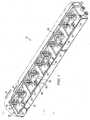
- FIG. 1there is generally shown at 10 a wideband dual polarized base station antenna having an optimized horizontal radiation pattern and also having a variable vertical beam tilt.
- Antenna 10is seen to include a plurality of element trays 12 having disposed thereon broadband slant 45 cross dipole (x-dipole) radiating elements 14 arranged in dipole pairs 16.
- Each of the element trays 12is tilted and arranged in a " fallen domino" arrangement and supported by a pair of tray supports 20.
- the integrated element trays 12 and tray supports 20are secured upon and within an external tray 22 such that there is a gap laterally defined between the tray supports 20 and the sidewalls of tray 22, as shown in Figure 1 and Figure 2 .
- Each tray element 12has an upper surface defining a groundplane for the respective dipole pair 16, and has a respective air dielectric micro stripline 30 spaced thereabove and feeding each of the dipole radiating elements 14 of dipole pairs 16, as shown.
- a plurality of electrically conductive arched straps 26are secured between the sidewalls of tray 22 to provide both rigidity of the antenna 10, and also to improve isolation between dipole radiating elements 14.
- a pair of cable supports 32extend above each tray element 12. Supports 32 support a respective low IM RF connection cables 34 from a cable 76 to the air dielectric micro stripline 30 and to microstrip feed network defined on a printed circuit board 50 adhered therebelow, as will be discussed in more detail shortly with reference to Figure 4 .
- FIG. 2there is shown a perspective view of the element trays 12 with the sidewall of one tray support 20 and tray 22 partially cut away to reveal the tilted tray elements 12 configured in the " fallen domino" arrangement.
- Each tray element 12is arranged in a this " fallen domino" arrangement so as to orient the respective dipole radiating element 14 pattern boresight at a predetermined downtilt, which may, for example, be the midpoint of the array adjustable tilt range.
- the desired maximum beam squint level of antenna 10 in this exampleis consistent with about 4° downtilt off of mechanical boresight, instead of about 8° off of mechanical boresight as would be the case without the tilt of the element trays 12.
- maximum horizontal beam squint levelshave been reduced to about 5° over conventional approaches, which is very acceptable considering the antenna's wide operating bandwidth and tilt range.
- the tray supports 20are separated from the respective adjacent sidewalls of tray 22 by an elongated gap defining an RF choke 36 therebetween.
- This choke 36 created by physical geometryadvantageously reduces the RF current that flows on the backside of the external tray 22.
- the reduction of induced currents on the backside of the external tray 22directly reduces radiation in the rear direction.
- the critical design criteria of this RF choke 36 involved in maximizing the radiation front-to-back ratioincludes the height of the folded up sidewalls 38 of external tray 22, the height of the tray supports 20, and the RF choke 36 between the tray supports 20 and the sidewall lips 38 of tray 22.
- the RF choke 36is preferably lambda /4 of the radiating element 14 center frequency, and the RF choke 36 has a narrow bandwidth which is frequency dependent because of internal reflection cancellation in the air dielectric, the choke bandwidth being about 22 percent of the center frequency.
- an RF absorber 39may be added into the RF choke 36 to make the RF choke less frequency dependent, and thus create a more broadband RF choke.
- the RF absorber 39preferably contains a high percentage of carbon that slows and dissipates any RF reflection wave from effecting the main beam radiation produced by the cross dipole antenna 12.
- the slant 45 cross dipole antenna 14, as shown,produces a cross polarized main beam radiation at a +/-45 degree orientation, each beam having a horizontal component and a vertical component. The cross polarization is good when these components are uniform and equal in magnitude in 360 degrees. For the panel antenna 10 shown in Figure 1 with the linearly arranged cross dipoles 14, the horizontal component of each beam orientation rolls off faster than the vertical component.
- the vertical beamwidthis broader than the horizontal beamwidth for each beam orientation, and the vertical components travel along the edge of the respective trays 12 more than the horizontal components. Because the thin metal trays 12 have limited surface area, the surface currents thereon are less likely to reflect the horizontal components back to the main beam radiation. In contrast, along the edges of the respective trays 12 the stair cased baffles 35 have to contain many of the vertical component vector currents.
- the RF absorber 39into the RF choke 36, the vertical components of each beam orientation are minimized from reflecting back into the main beam radiation of the cross dipole 14. As such, cross dipoles 14 are not provided with a reflector behind them.
- the element trays 12are fabricated from brass alloy and are treated with a tin plating finish for solderability.
- the primary function of the element traysis to support the radiating element 14 in a specific orientation, as shown. This orientation provides more optimally balanced vertical and horizontal beam patterns for both ports of the antenna 10. This orientation also provides improved isolation between each port. Additionally, the element trays 12 provide an RF grounding point at the coaxial cable/airstrip interface.
- the tray supportsare preferably fabricated from aluminum alloy.
- the primary function of the tray supportsis to support the five element trays 12 in a specific orientation that minimizes horizontal pattern beam squint.
- the external tray 22is preferably fabricated from a thicker stock of aluminum alloy than element trays 12, and is preferably treated with an alodine coating to prevent corrosion due to external environment conditions.
- a primary functions of the external tray 22is to support the internal array components.
- a secondary functionis to focus the radiated RF power toward the forward sector of the antenna 10 by minimizing radiation toward the back, thereby maximizing the radiation pattern front-to-back ratio, as already discussed.
- Nis 1,2,3,4», where N is shown to equal 4 in this embodiment.
- the upper laterally extending members of parasitic broadband cross dipole director 40are preferably uniformly spaced from one another, with the upper members preferably having a shorter length, as shown for bandwidth broadening.
- the lower members of director 40are more closely spaced from the radiating element 14, so as to properly couple the RF energy to the director in a manner that provides pattern enhancement while maintaining an efficient impedance match such that substantially no gain is realized by the director 40, unlike a Yagi-Uda antenna having a reflector and spaced elements each creating gain.
- an improved pattern rolloffis achieved beyond the 3dB beamwidth of the radiation pattern while maintaining a similar 3dB beamwidth.
- the upper elements of directors 40are spaced about .033 lambda (center frequency) from one another, with the lower director elements spaced from the radiating element 14 about .025 lambda by parasitic 42 (lambda being the wavelength of the center frequency of the radiating element 14 design).
- PCB 50low loss printed circuit board
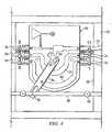
- microstrip capacitive phase shifter system 52is coupled to and feeds the opposing respective pair of radiating elements 14 via the respective cables 34.
- each microstrip phase shifter system 52comprises a phase shifter wiper arm 56 having secured thereunder a dielectric member 54 which is arcuately adjustable about a pivot point 58 by a respective shifter rod 60.
- Shifter rod 60is longitudinally adjustable by a remote handle (not shown) so as to selectively position the phase shifter wiper arm 56 and the respective dielectric 54 across a pair of arcuate feedline portions 62 and 64 to adjust the phase velocity conducting therethrough.
- Shifter rod 60is secured to, but spaced above, PCB 50 by a pair of non-conductive standoffs 66.
- the low loss coaxial cables 34are employed as the main transmission media providing electrical connection between the phase shifter system 52 and the radiating elements 14. Gain performance is optimized by closely controlling the phase and amplitude distribution across the radiating elements 14 of antenna 10. The very stable phase shifter design shown in Figure 4 achieves this control.
- each microstrip phase shifter system 52feeding one of the other polarized antennas 14.
- Input 72is referred as port I and is the input for the -45 polarized Slant
- input 74is the port II input for the +45 polarized Slant.
- Cables 76are the feed lines coupled to one respective phase shifter system 52, as shown in Figure 4 .
- the outputs of phase shifter system 52depicted as outputs 1-5, indicate the dipole pair 16 that is fed by the respective output of the phase shifter 52 system.
- antenna 10further including an RF absorber 78 positioned under each of the element trays 12, behind antenna 10, that functions to dissipate any rearward RF radiation from the phase shifter microstrip lines, and preventing RF current from coupling between phase shifters systems 52.
- RF absorber 78positioned under each of the element trays 12, behind antenna 10, that functions to dissipate any rearward RF radiation from the phase shifter microstrip lines, and preventing RF current from coupling between phase shifters systems 52.
- FIG. 7there is generally shown at 68 the high roll-off and front-to-back ratio radiation pattern achieved by antenna 10 according to the present invention, as compared to a standard 65° panel antenna having a dipole radiation pattern shown at 69.
- This high roll-off radiation pattern 68is a significant improvement over the typical dipole radiation pattern 69.
- the horizontal beam widthstill holds at approximately 65 degree at the 3 dB point.
- the design of the radiating elements 14 with directors 40provides dramatic improvements in the antenna's horizontal beam radiation pattern, "where the Front-to-Side levels are shown to be 23dB in Figure 7 .
- Conventional, cross dipole radiating elementsproduce a horizontal beam radiation pattern with about a 17 dB front-to-side ratio, as shown in Figure 7 .
- the broadband parasitic directors 40 integrated above the radiating elements 14advantageously improve the antenna front-to-side ratio by up to 10 dB, and is shown as 6dB delta in the example of Figure 7 .
- This improved front-to-side ratio effectis referred to as a "high roll-off" design.
- radiating elements 14 and cross dipole directors 40advantageously maintain an approximately 65 degree horizontal beamwidth at the antenna's 3 dB point, unlike any conventional Yagi-Uda antenna having more directors to get more gain and thus reducing the horizontal beamwidth.
- FIG. 7there is shown the excellent front-to-back ratio of antenna 10.
- panel antenna 10has a substantially reduced backside lobe, thus achieving a front-to-back ratio of about 40 dB.
- antenna 10has a next sector antenna/antenna isolation of about 40 dB, as compared to 26 dB for the standard 65° panel antenna.
- a 120° sector interference free zoneis provided behind the radiation lobe, referred to in the present invention as the "cone of silence”.
- Figure 8A and 8Bthere is shown several advantages of the present invention when employed in a three sector site.
- Figure 8Adepicts standard 65° flat panel antennas used in a three sector site
- Figure 8Bdepicts standard 90° panel antennas used in a three sector site.
- the significant overlap of these antenna radiation patternscreates imperfect sectorization that presents opportunities for increased softer hand-offs, interfering signals, dropped calls, and reduced capacity.
- FIG. 9A and 9Bthere is shown technical advantages of the present invention utilizing a 65° panel antenna and a 90° panel antenna, respectively according to the present invention, employed in a three sector site.
- Figure 9Athere is depicted significantly reduced overlap of the antenna radiation lobes, thus realizing a much smaller hand-off area. This leads to dramatic call quality improvement, and further, a 5-10% site capacity enhancement.
- the undesired lobe extending beyond the 120° sector of radiationcreates overlap with adjacent antenna radiation patterns, as shown in Figure 8A-8B and Figure 9A-9B .
- SPRSector Power Ratio
- the directors 40are impedance matched at 90 ohms, although limitation to this impedance is not inferred, to the micro stripline 30.
- the radiating elements 14 and the cross dipole directors 40have mutual instantaneous electromagnetic coupling which generate with source impedance at 90 ohm and source voltage of a matching network.
- Many other system level performance benefitsare afforded by incorporation of this high roll-off antenna design, including improved soft handoff capabilities, reduced co-site channel interference and increased base station system capacity due to increased sector-to-sector rejection.
- the N directors 82are configured as vertically spaced parallel polygon-shaped members, shown as concentric rings, although limitation to this geometry of directors 82 is not to be inferred. Other geometric configurations of the directors may be utilized as shown in Figure 13 .
- the ring directors 82react with the corresponding dipole radiating element 14 to enhance the front-to-side ratio of antenna 10 with improved rolloff.
- the ring directors 82are preferably uniformly spaced above the corresponding x-dipole radiating element 14, with the ascending ring directors 82 having a continually smaller circumference.
- the ring directors 82maintain a relatively close spacing with one another being separated by electrically non-conductive spacers, not shown, preferably being spaced less than 0.15 lambda (lambda being the wavelength of the center frequency of the antenna design). Additionally, the grouping of ring directors 82 maintain a relatively close spacing between the bottommost director 82 and the top of the corresponding dipole radiating element 14, preferably less than 0.15 lambda.
- There are a variety of methods to build the set of planar directors 82such as molded forms and electrically insulating clips.
- the set of stacked ring directors 82may also consist of rings of equal circumference while maintaining similar performance of improved roll-off leading to an improved SPR with the previously stated system benefits while maintaining a similar 3dB beamwidth.
- a dual-band antennaincluding a set of director rings 92 disposed above a stacked Microstrip Annular Ring (MAR) radiator 94.
- MARMicrostrip Annular Ring
- the directors 92 in this embodiment of the inventionare thin rings stacked above the respective MAR radiator 94, as shown.
- this dual-band antenna 90also has improved element pattern roll-off beyond the 3dB beamwidth thus increasing the SPR while maintaining an equivalent 3dB beamwidth.
- a dual-band antenna 100having ring directors 82 and 92.
- the ring directors 92 above the MAR radiator 94also interact with the x-dipole radiating element 14 and provide some additional beamshaping for the x-dipole radiating element, including improved roll-off of the main beam outside of the 3dB beamwidth as well as improved front-to-back-radiation leading to an improved SPR and the system benefits previously mentioned while maintaining a similar 3dB beamwidth.
- Both the MAR radiator element 94 and the x-dipole radiating element 14have respective ring directors thereabove.
- the ring directors 82 for the x-dipole radiating element 14are also concentric to the ring directors 92 for the MAR radiator 94.
- the same benefits as discussed earlier for the directorsare applicable here as well per frequency band (i.e. improved roll-off beyond the 3dB beamwidth and front-to-back ratio leading to improved SPR.
- FIG. 13there is shown other suitable geometrical configurations of directors 82 and 92, and limitation to a circular ring-like director is not to be inferred.
- a circleis considered to be an infinitely sided polygon where the term polygon is used in the appending claims.
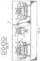
- FIG. 14there is shown a close-up view of dual band antenna 80 having cross shaped directors 40 extending over the radiating element 14, and the MAR radiator 94 without the associated annular director.
- a panel antenna 110having an array of radiating elements 14, each having cross directors 40, alternately provided with the MAR radiators 94, each disposed over common groundplane 112.
- the advantages of this designinclude an improved H-plane pattern for the higher frequency radiating element in a dualband topology.
- the improved H-plane patternprovides improved roll-off beyond the 3dB beamwidth and improved front-to-back ratio.
- the improved roll-offadditionally provides a slight decoupling of the radiators depending on the number of directors incorporated due to lower levels of side and back radiation.
Landscapes
- Variable-Direction Aerials And Aerial Arrays (AREA)
- Aerials With Secondary Devices (AREA)
Description
- The present invention is related to the field of antennas, and more particularly to antennas having dipole radiating elements utilized in wireless communication systems.
- Wireless mobile communication networks continue to be deployed and improved upon given the increased traffic demands on the networks, the expanded coverage areas for service and the new systems being deployed. Cellular type communication systems derive their name in that a plurality of antenna systems, each serving a sector or area commonly referred to as a cell, are implemented to effect coverage for a larger service area. The collective cells make up the total service area for a particular wireless communication network.
- Serving each cell is an antenna array and associated switches connecting the cell into the overall communication network. Typically, the antenna array is divided into sectors, where each antenna serves a respective sector. For instance, three antennas of an antenna system may serve three sectors, each having a range of coverage of about 120°. These antennas are typically vertically polarized and have some degree of downtilt such that the radiation pattern of the antenna is directed slightly downwardly towards the mobile handsets used by the customers. This desired downtilt is often a function of terrain and other geographical features. However, the optimum value of downtilt is not always predictable prior to actual installation and testing. Thus, there is always the need for custom setting of each antenna downtilt upon installation of the actual antenna. Typically, high capacity cellular type systems can require re-optimization during a 24 hour period. In addition, customers want antennas with the highest gain for a given size and with very little intermodulation (IM). Thus, the customer can dictate which antenna is best for a given network implementation.
- European
patent application EP 1 156 549 and United States Patent applicationUS 5,952,983 describe a system incorporating slant 45 antennae. United States patentUS 4,218,686 and German patent applicationDE 4443055 disclose the use of directors in systems using conventional Yagi-type antennae. - It is a further objective of the invention to provide a dual polarized antenna having improved directivity and providing improved sector isolation to realize an improved Sector Power Ratio (SPR).
- It is an objective of the present invention to provide a dual polarized antenna array having optimized horizontal plane radiation patterns. One objective is to provide a radiation pattern having at least a 20 dB horizontal beam front-to-side ratio, at least a 40 dB horizontal beam front-to-back ratio, and improved roll-off.
- It is another objective of the invention to provide an antenna array with optimized cross polarization performance with a minimum of 10 dB co-pol to cross-pol ratio in a 120 degree horizontal sector.
- It is another objective of the invention to provide an antenna array with a horizontal pattern beamwidth of 50° to 75°.
- It is another objective of the invention to provide an antenna array with minimized intermodulation.
- It is an objective of the invention to provide a dual polarized antenna array capable of operating over an expanded frequency range.
- It is a further objective of the invention to provide a dual polarized antenna array capable of producing adjustable vertical plane radiation patterns.
- It is another objective of the invention to provide an antenna with enhanced port to port isolation of at least 30 dB.
- It is further object of the invention to provide an inexpensive antenna.
- These and other objectives of the invention are provided by an improved antenna array for transmitting and receiving electromagnetic waves with +45° and -45° linear polarizations.
- Viewed from a first aspect, the present invention relates to an antenna array having multiple antennas each serving a respective sector, each antenna being for transmitting and receiving electromagnetic waves with +45° and -45° linear polarizations and comprising:
- a plurality of element trays each having disposed thereon a dipole pair of slant 45 cross dipole radiating elements;
- the slant 45 cross dipole radiating elements each being adapted to generate a beam having a 3db beamwidth and a Sector Power Ratio, SPR, defined as:

- characterised by:
- the slant 45 cross dipole radiating elements each having directors including, relative to the element tray on which the slant 45 cross dipole radiating element is disposed, a bottommost director spaced less than 0.15 lambda from the top of the slant 45 cross dipole radiating element so as to reduce the SPR of the beam while maintaining the 3dB beamwidth, wherein lambda is the wavelength of the centre frequency of the slant 45 cross dipole radiating element and wherein the element trays are tilted in a fallen-domino arrangement so as to orient the dipole pairs of slant 45 cross dipole radiating elements such that they have a boresight at a predetermined downtilt.
Figure 1 is a perspective view of a dual polarized antenna according to a first preferred embodiment of the present invention;Figure 2 is a perspective view of a multi-level groundplane structure with a broadband slant 45 cross dipole radiating element removed therefrom, and a tray cutaway to illustrate a tilting of the groundplanes and an RF absorber in a RF choke;Figure 3 is a perspective view of N cross-shaped directors supported above the dipole radiating element;Figure 4 is a backside view of one element tray illustrating a microstrip phase shifter design employed to feed each pair of the cross dipole radiating elements;Figure 5 is a backside view of the dual polarized antenna illustrating the cable feed network, each microstrip phase shifter feeding one of the other dual polarized antennas;Figure 6 is a perspective view of the dual polarized antenna including an RF absorber functioning to dissipate RF radiation from the phase shifter microstriplines, and preventing the RF current cross coupling;Figure 7 is a graph depicting the high roll-off radiation pattern achieved by the present invention, as compared to a typical cross dipole antenna radiation pattern;Figure 8A and 8B are graphs depicting the beam patterns in a three sector site utilizing standard panel antennas;Figure 9A and 9B are graphs depicting the beam patterns in a three sector site utilizing antennas according to the present invention;Figure 10 is a perspective view of another embodiment of the invention including dual-band radiating elements;Figure 11 is a perspective view of the embodiment shown inFigure 10 having director rings disposed over one of the radiating elements;Figure 12 is a perspective view of an embodiment of the invention having director rings disposed over each of the radiating elements;Figure 13 is a view of various suitable configurations of directors;Figure 14 is a close-up view of a dual-band antenna; andFigure 15 depicts an array of dual-band and single-band dipole radiating elements.- Referring now to
Figure 1 , there is generally shown at 10 a wideband dual polarized base station antenna having an optimized horizontal radiation pattern and also having a variable vertical beam tilt.Antenna 10 is seen to include a plurality ofelement trays 12 having disposed thereon broadband slant 45 cross dipole (x-dipole) radiatingelements 14 arranged indipole pairs 16. Each of theelement trays 12 is tilted and arranged in a "fallen domino" arrangement and supported by a pair oftray supports 20. The integratedelement trays 12 andtray supports 20 are secured upon and within anexternal tray 22 such that there is a gap laterally defined between the tray supports 20 and the sidewalls oftray 22, as shown inFigure 1 andFigure 2 . Eachtray element 12 has an upper surface defining a groundplane for therespective dipole pair 16, and has a respective air dielectricmicro stripline 30 spaced thereabove and feeding each of thedipole radiating elements 14 ofdipole pairs 16, as shown. A plurality of electrically conductivearched straps 26 are secured between the sidewalls oftray 22 to provide both rigidity of theantenna 10, and also to improve isolation betweendipole radiating elements 14. - As shown, a pair of cable supports 32 extend above each
tray element 12. Supports 32 support a respective low IMRF connection cables 34 from acable 76 to the air dielectricmicro stripline 30 and to microstrip feed network defined on a printedcircuit board 50 adhered therebelow, as will be discussed in more detail shortly with reference toFigure 4 . - Referring now to
Figure 2 , there is shown a perspective view of theelement trays 12 with the sidewall of onetray support 20 andtray 22 partially cut away to reveal the tiltedtray elements 12 configured in the "fallen domino" arrangement. Eachtray element 12 is arranged in a this "fallen domino" arrangement so as to orient the respectivedipole radiating element 14 pattern boresight at a predetermined downtilt, which may, for example, be the midpoint of the array adjustable tilt range. The desired maximum beam squint level ofantenna 10 in this example is consistent with about 4° downtilt off of mechanical boresight, instead of about 8° off of mechanical boresight as would be the case without the tilt of theelement trays 12. According to the present invention, maximum horizontal beam squint levels have been reduced to about 5° over conventional approaches, which is very acceptable considering the antenna's wide operating bandwidth and tilt range. - Still referring to
Figure 2 , there is illustrated that the tray supports 20 are separated from the respective adjacent sidewalls oftray 22 by an elongated gap defining anRF choke 36 therebetween. Thischoke 36 created by physical geometry advantageously reduces the RF current that flows on the backside of theexternal tray 22. The reduction of induced currents on the backside of theexternal tray 22 directly reduces radiation in the rear direction. The critical design criteria of this RF choke 36 involved in maximizing the radiation front-to-back ratio includes the height of the folded up sidewalls 38 ofexternal tray 22, the height of the tray supports 20, and theRF choke 36 between the tray supports 20 and thesidewall lips 38 oftray 22. TheRF choke 36 is preferably lambda /4 of the radiatingelement 14 center frequency, and theRF choke 36 has a narrow bandwidth which is frequency dependent because of internal reflection cancellation in the air dielectric, the choke bandwidth being about 22 percent of the center frequency. - According to a further embodiment of the present invention, an
RF absorber 39 may be added into theRF choke 36 to make the RF choke less frequency dependent, and thus create a more broadband RF choke. TheRF absorber 39 preferably contains a high percentage of carbon that slows and dissipates any RF reflection wave from effecting the main beam radiation produced by thecross dipole antenna 12. The slant 45cross dipole antenna 14, as shown, produces a cross polarized main beam radiation at a +/-45 degree orientation, each beam having a horizontal component and a vertical component. The cross polarization is good when these components are uniform and equal in magnitude in 360 degrees. For thepanel antenna 10 shown inFigure 1 with the linearly arrangedcross dipoles 14, the horizontal component of each beam orientation rolls off faster than the vertical component. This means that the vertical beamwidth is broader than the horizontal beamwidth for each beam orientation, and the vertical components travel along the edge of therespective trays 12 more than the horizontal components. Because thethin metal trays 12 have limited surface area, the surface currents thereon are less likely to reflect the horizontal components back to the main beam radiation. In contrast, along the edges of therespective trays 12 the stair cased baffles 35 have to contain many of the vertical component vector currents. Advantageously, by adding theRF absorber 39 into theRF choke 36, the vertical components of each beam orientation are minimized from reflecting back into the main beam radiation of thecross dipole 14. As such,cross dipoles 14 are not provided with a reflector behind them. - Preferably, the
element trays 12 are fabricated from brass alloy and are treated with a tin plating finish for solderability. The primary function of the element trays is to support the radiatingelement 14 in a specific orientation, as shown. This orientation provides more optimally balanced vertical and horizontal beam patterns for both ports of theantenna 10. This orientation also provides improved isolation between each port. Additionally, theelement trays 12 provide an RF grounding point at the coaxial cable/airstrip interface. - The tray supports are preferably fabricated from aluminum alloy. The primary function of the tray supports is to support the five
element trays 12 in a specific orientation that minimizes horizontal pattern beam squint. - The
external tray 22 is preferably fabricated from a thicker stock of aluminum alloy thanelement trays 12, and is preferably treated with an alodine coating to prevent corrosion due to external environment conditions. A primary functions of theexternal tray 22 is to support the internal array components. A secondary function is to focus the radiated RF power toward the forward sector of theantenna 10 by minimizing radiation toward the back, thereby maximizing the radiation pattern front-to-back ratio, as already discussed. - Referring now to
Figure 3 there is depicted oneradiator element 14 having N laterally extending parasitic broadbandcross dipole directors 40 disposed above the radiatingelement 14 and fed by theairstrip feed network 30, as shown. N is 1,2,3,4......, where N is shown to equal 4 in this embodiment. The upper laterally extending members of parasitic broadbandcross dipole director 40 are preferably uniformly spaced from one another, with the upper members preferably having a shorter length, as shown for bandwidth broadening. The lower members ofdirector 40 are more closely spaced from the radiatingelement 14, so as to properly couple the RF energy to the director in a manner that provides pattern enhancement while maintaining an efficient impedance match such that substantially no gain is realized by thedirector 40, unlike a Yagi-Uda antenna having a reflector and spaced elements each creating gain. Advantageously, rather than realized gain, an improved pattern rolloff is achieved beyond the 3dB beamwidth of the radiation pattern while maintaining a similar 3dB beamwidth. Preferably, the upper elements ofdirectors 40 are spaced about .033 lambda (center frequency) from one another, with the lower director elements spaced from the radiatingelement 14 about .025 lambda by parasitic 42 (lambda being the wavelength of the center frequency of the radiatingelement 14 design). - Referring now to
Figure 4 there is shown one low loss printed circuit board (PCB) 50 having disposed thereon a microstrip capacitive phase shifter system generally shown at 52. Thelow loss PCB 50 is secured to the backside of therespective element tray 12. Microstrip capacitivephase shifter system 52 is coupled to and feeds the opposing respective pair of radiatingelements 14 via therespective cables 34. - As shown in
Figure 4 , each microstripphase shifter system 52 comprises a phaseshifter wiper arm 56 having secured thereunder adielectric member 54 which is arcuately adjustable about apivot point 58 by arespective shifter rod 60.Shifter rod 60 is longitudinally adjustable by a remote handle (not shown) so as to selectively position the phaseshifter wiper arm 56 and therespective dielectric 54 across a pair ofarcuate feedline portions 62 and 64 to adjust the phase velocity conducting therethrough.Shifter rod 60 is secured to, but spaced above,PCB 50 by a pair ofnon-conductive standoffs 66. The low losscoaxial cables 34 are employed as the main transmission media providing electrical connection between thephase shifter system 52 and the radiatingelements 14. Gain performance is optimized by closely controlling the phase and amplitude distribution across the radiatingelements 14 ofantenna 10. The very stable phase shifter design shown inFigure 4 achieves this control. - Referring now to
Figure 5 , there is shown the backside of theantenna 10 illustrating the cable feed network, each microstripphase shifter system 52 feeding one of the otherpolarized antennas 14.Input 72 is referred as port I and is the input for the -45 polarized Slant, andinput 74 is the port II input for the +45 polarized Slant.Cables 76 are the feed lines coupled to one respectivephase shifter system 52, as shown inFigure 4 . The outputs ofphase shifter system 52, depicted as outputs 1-5, indicate thedipole pair 16 that is fed by the respective output of thephase shifter 52 system. - Referring now to
Figure 6 , there is shownantenna 10 further including anRF absorber 78 positioned under each of theelement trays 12, behindantenna 10, that functions to dissipate any rearward RF radiation from the phase shifter microstrip lines, and preventing RF current from coupling betweenphase shifters systems 52. - Referring now to
Figure 7 , there is generally shown at 68 the high roll-off and front-to-back ratio radiation pattern achieved byantenna 10 according to the present invention, as compared to a standard 65° panel antenna having a dipole radiation pattern shown at 69. This high roll-off radiation pattern 68 is a significant improvement over the typicaldipole radiation pattern 69. The horizontal beam width still holds at approximately 65 degree at the 3 dB point. - Further, the design of the radiating
elements 14 withdirectors 40 provides dramatic improvements in the antenna's horizontal beam radiation pattern, "where the Front-to-Side levels are shown to be 23dB inFigure 7 . Conventional, cross dipole radiating elements produce a horizontal beam radiation pattern with about a 17 dB front-to-side ratio, as shown inFigure 7 . According to the present invention, the broadbandparasitic directors 40 integrated above the radiatingelements 14 advantageously improve the antenna front-to-side ratio by up to 10 dB, and is shown as 6dB delta in the example ofFigure 7 . This improved front-to-side ratio effect is referred to as a "high roll-off" design. In this embodiment, radiatingelements 14 andcross dipole directors 40 advantageously maintain an approximately 65 degree horizontal beamwidth at the antenna's 3 dB point, unlike any conventional Yagi-Uda antenna having more directors to get more gain and thus reducing the horizontal beamwidth. - Still referring to
Figure 7 , there is shown the excellent front-to-back ratio ofantenna 10. As shown,panel antenna 10 has a substantially reduced backside lobe, thus achieving a front-to-back ratio of about 40 dB. Moreover,antenna 10 has a next sector antenna/antenna isolation of about 40 dB, as compared to 26 dB for the standard 65° panel antenna. As can also be appreciated inFigure 7 , with the significant reduction of a rear lobe, a 120° sector interference free zone is provided behind the radiation lobe, referred to in the present invention as the "cone of silence". - Referring now to
Figure 8A and 8B , there is shown several advantages of the present invention when employed in a three sector site.Figure 8A depicts standard 65° flat panel antennas used in a three sector site, andFigure 8B depicts standard 90° panel antennas used in a three sector site. The significant overlap of these antenna radiation patterns creates imperfect sectorization that presents opportunities for increased softer hand-offs, interfering signals, dropped calls, and reduced capacity. - Referring now to
Figure 9A and 9B , there is shown technical advantages of the present invention utilizing a 65° panel antenna and a 90° panel antenna, respectively according to the present invention, employed in a three sector site. With respect toFigure 9A , there is depicted significantly reduced overlap of the antenna radiation lobes, thus realizing a much smaller hand-off area. This leads to dramatic call quality improvement, and further, a 5-10% site capacity enhancement. - Referring back to
Figure 7 , the undesired lobe extending beyond the 120° sector of radiation creates overlap with adjacent antenna radiation patterns, as shown inFigure 8A-8B and Figure 9A-9B . The undesired power delivered in the lobe outside of the 120° forward sector edges, as compared to that desired power delivered inside this 120° sector, defines what is referred to as the Sector Power Ratio (SPR). Advantageously, the present invention achieves a SPR being less than 2%, where the SPR is defined by the following equation:
- This SPR is a significant improvement over standard panel antennas, and is one measure of depicting the technical advantages of the present invention. The
directors 40 are impedance matched at 90 ohms, although limitation to this impedance is not inferred, to themicro stripline 30. The radiatingelements 14 and thecross dipole directors 40 have mutual instantaneous electromagnetic coupling which generate with source impedance at 90 ohm and source voltage of a matching network. Many other system level performance benefits are afforded by incorporation of this high roll-off antenna design, including improved soft handoff capabilities, reduced co-site channel interference and increased base station system capacity due to increased sector-to-sector rejection. - Referring now to
Figure 10 , there is shown another preferred embodiment of the invention seen to comprise a band,dualpol antenna 80 including one slant 45 crosseddipole radiating element 14 and a slant 45 microstrip Annular Ring (MAR)radiator 94 encircling said dipole, as will be described shortly in reference toFigure 11 . In this embodiment,antenna 80 includes N annular (ring-like)directors 82 disposed above the radiatingelement 14, where N = 1,2,3,4.... TheN directors 82 are configured as vertically spaced parallel polygon-shaped members, shown as concentric rings, although limitation to this geometry ofdirectors 82 is not to be inferred. Other geometric configurations of the directors may be utilized as shown inFigure 13 . - The
ring directors 82 react with the correspondingdipole radiating element 14 to enhance the front-to-side ratio ofantenna 10 with improved rolloff. Thering directors 82 are preferably uniformly spaced above the correspondingx-dipole radiating element 14, with the ascendingring directors 82 having a continually smaller circumference. Thering directors 82 maintain a relatively close spacing with one another being separated by electrically non-conductive spacers, not shown, preferably being spaced less than 0.15 lambda (lambda being the wavelength of the center frequency of the antenna design). Additionally, the grouping ofring directors 82 maintain a relatively close spacing between thebottommost director 82 and the top of the correspondingdipole radiating element 14, preferably less than 0.15 lambda. There are a variety of methods to build the set ofplanar directors 82, such as molded forms and electrically insulating clips. - The set of stacked
ring directors 82 may also consist of rings of equal circumference while maintaining similar performance of improved roll-off leading to an improved SPR with the previously stated system benefits while maintaining a similar 3dB beamwidth. - Referring now to
Figure 11 , there is shown at 90 a dual-band antenna including a set of director rings 92 disposed above a stacked Microstrip Annular Ring (MAR)radiator 94. In this view, there are four feedprobes 96 (2 balanced feed pairs) arranged in pairs feeding dual orthogonal polarizations of theMAR radiator 94. Thedirectors 92 in this embodiment of the invention are thin rings stacked above therespective MAR radiator 94, as shown. Advantageously, this dual-band antenna 90 also has improved element pattern roll-off beyond the 3dB beamwidth thus increasing the SPR while maintaining an equivalent 3dB beamwidth. - Referring now to
Figure 12 , there is shown a dual-band antenna 100 havingring directors ring directors 92 above theMAR radiator 94 also interact with thex-dipole radiating element 14 and provide some additional beamshaping for the x-dipole radiating element, including improved roll-off of the main beam outside of the 3dB beamwidth as well as improved front-to-back-radiation leading to an improved SPR and the system benefits previously mentioned while maintaining a similar 3dB beamwidth. - Both the
MAR radiator element 94 and thex-dipole radiating element 14 have respective ring directors thereabove. Thering directors 82 for thex-dipole radiating element 14 are also concentric to thering directors 92 for theMAR radiator 94. The same benefits as discussed earlier for the directors are applicable here as well per frequency band (i.e. improved roll-off beyond the 3dB beamwidth and front-to-back ratio leading to improved SPR. - Referring now to
Figure 13 , there is shown other suitable geometrical configurations ofdirectors - Referring now to
Figure 14 , there is shown a close-up view ofdual band antenna 80 having cross shapeddirectors 40 extending over the radiatingelement 14, and theMAR radiator 94 without the associated annular director. - Referring now to
Figure 15 , there is shown apanel antenna 110 having an array of radiatingelements 14, each havingcross directors 40, alternately provided with theMAR radiators 94, each disposed overcommon groundplane 112. The advantages of this design include an improved H-plane pattern for the higher frequency radiating element in a dualband topology. The improved H-plane pattern provides improved roll-off beyond the 3dB beamwidth and improved front-to-back ratio. The improved roll-off additionally provides a slight decoupling of the radiators depending on the number of directors incorporated due to lower levels of side and back radiation. - Though the invention has been described with respect to a specific preferred embodiment, many variations and modifications will become apparent to those skilled in the art upon reading the present application. It is therefore the intention that the appended claims be interpreted as broadly as possible in view of the prior art to include all such variations and modifications.


Claims (17)
- An antenna array having multiple antennas (10) each serving a respective sector, each antenna (10) being for transmitting and receiving electromagnetic waves with +45° and -45° linear polarizations and comprising:a plurality of element trays (12) each having disposed thereon a dipole pair of slant 45 cross dipole radiating elements (14);the slant 45 cross dipole radiating elements (14) each being adapted to generate a beam having a 3db beamwidth and a Sector Power Ratio, SPR, defined as:
 characterised by:the slant 45 cross dipole radiating elements (14) each having directors (40; 82; 92) including, relative to the element tray (12) on which the slant 45 cross dipole radiating element (14) is disposed, a bottommost director (40; 82; 92) spaced less than 0.15 lambda from the top of the slant 45 cross dipole radiating element (14) so as to reduce the SPR of the beam while maintaining the 3dB beamwidth, wherein lambda is the wavelength of the centre frequency of the slant 45 cross dipole radiating element (14) and wherein the element trays (12) are tilted in a fallen-domino arrangement so as to orient the dipole pairs of slant 45 cross dipole radiating elements (14) such that they have a boresight at a predetermined downtilt.
 - The antenna array as specified in Claim 1, wherein the directors (40; 82; 92) of a respective one of the slant 45 cross dipole radiating elements (14) are parallel to one another.
- The antenna array as specified in Claim 1, wherein at least some of the directors (40; 82; 92) of a respective one of the slant 45 cross dipole radiating elements (14) are uniformly spaced from one another.
- The antenna array as specified in Claim 3, wherein the bottommost director (40; 82; 92) of a respective one of the slant 45 cross dipole radiating elements (14) is spaced closer to the slant 45 cross dipole radiating element (14) than to an adjacent one of the directors (40; 82; 92) of the slant 45 cross dipole radiating element (14).
- The antenna array as specified in Claim 1, wherein the directors (40; 82; 92) of a respective one of the slant 45 cross dipole radiating elements (14) are spaced about 0.033 lambda from one another.
- The antenna array as specified in any one of the preceding claims, wherein the bottommost director (40; 82; 92) is spaced from the slant 45 cross dipole radiating element (14) by 0.025 lambda.
- The antenna array as specified in Claim 1, wherein the bottommost director (40; 82; 92) has at least two members.
- The antenna array as specified in Claim 7, wherein the members are cross-shaped members parallel to the slant 45 cross dipole radiating element (14) in the vertical direction.
- The antenna array as specified in Claim 1, wherein the bottommost director (40; 82; 92) comprises a polygon shaped ring.
- The antenna array as specified in Claim 9, further comprising a plurality of polygon shaped rings disposed over the at least one slant 45 cross dipole radiating element (14).
- The antenna array as specified in Claim 10, wherein the polygon shaped rings are concentric.
- The antenna array as specified in Claim 11, wherein the polygon shaped rings have a common diameter.
- The antenna array as specified in Claim 10, wherein the polygon shaped rings have different diameters and form a tapered director.
- The antenna array as specified in Claim 7, wherein the members have different lengths and form a tapered director.
- The antenna array as specified in any one of the preceding claims, wherein a first one of the slant 45 cross dipole radiating elements (14) is adapted to generate its beam at a first frequency and a second one of the slant 45 cross dipole radiating elements (14) disposed proximate the first one of the slant 45 cross dipole radiating elements (14) is adapted to generate its beam at a second frequency,
wherein the antenna (10) is a dual band antenna. - The antenna array as specified in any one of the preceding claims, comprising a microstrip capacitive phase shifter system electrically connected to the dipole pairs of slant 45 cross dipole radiating elements (14) to control the phase and amplitude distribution across the dipole pairs of slant 45 cross dipole radiating elements (14) to adjust the vertical plane radiation pattern.
- The antenna array as specified in any one of the preceding claims, comprising a tray (22) having a backside with the element trays (12) disposed above, the tray (22) having a side wall spaced from the element trays (12) and defining a gap therebetween.

Applications Claiming Priority (3)
| Application Number | Priority Date | Filing Date | Title |
|---|---|---|---|
| US57713804P | 2004-06-04 | 2004-06-04 | |
| US73721404A | 2004-12-16 | 2004-12-16 | |
| PCT/US2005/012528WO2005122331A1 (en) | 2004-06-04 | 2005-04-13 | Directed dipole antenna |
Publications (2)
| Publication Number | Publication Date |
|---|---|
| EP1751821A1 EP1751821A1 (en) | 2007-02-14 |
| EP1751821B1true EP1751821B1 (en) | 2016-03-09 |
Family
ID=34968962
Family Applications (1)
| Application Number | Title | Priority Date | Filing Date |
|---|---|---|---|
| EP05746446.3AExpired - LifetimeEP1751821B1 (en) | 2004-06-04 | 2005-04-13 | Directive dipole antenna |
Country Status (4)
| Country | Link |
|---|---|
| EP (1) | EP1751821B1 (en) |
| JP (1) | JP2008507163A (en) |
| KR (1) | KR101085814B1 (en) |
| WO (1) | WO2005122331A1 (en) |
Cited By (1)
| Publication number | Priority date | Publication date | Assignee | Title |
|---|---|---|---|---|
| EP4383460A3 (en)* | 2022-12-09 | 2024-08-14 | Fuba Automotive Electronics GmbH | Satellite antenna |
Families Citing this family (31)
| Publication number | Priority date | Publication date | Assignee | Title |
|---|---|---|---|---|
| US7868843B2 (en) | 2004-08-31 | 2011-01-11 | Fractus, S.A. | Slim multi-band antenna array for cellular base stations |
| ES2380580T3 (en) | 2005-10-14 | 2012-05-16 | Fractus S.A. | Small triple band antenna training for cellular base stations |
| ITTO20080473A1 (en) | 2008-06-17 | 2009-12-18 | Fracarro Radioindustrie Spa | ANTENNA |
| WO2010018896A1 (en)* | 2008-08-11 | 2010-02-18 | Ace Antenna Corp. | Antenna having a decoupling element |
| KR101027374B1 (en)* | 2008-08-11 | 2011-04-11 | 주식회사 에이스테크놀로지 | Antenna with decoupling element |
| FR2939569B1 (en)* | 2008-12-10 | 2011-08-26 | Alcatel Lucent | RADIANT ELEMENT WITH DUAL POLARIZATION FOR BROADBAND ANTENNA. |
| EP2256860B1 (en)* | 2009-05-26 | 2018-12-19 | Alcatel Lucent | Antenna array |
| JP5195783B2 (en)* | 2010-02-18 | 2013-05-15 | 住友電気工業株式会社 | Distribution phase shifter |
| US8854275B2 (en) | 2011-03-03 | 2014-10-07 | Tangitek, Llc | Antenna apparatus and method for reducing background noise and increasing reception sensitivity |
| US9055667B2 (en) | 2011-06-29 | 2015-06-09 | Tangitek, Llc | Noise dampening energy efficient tape and gasket material |
| US8164527B2 (en)* | 2011-03-03 | 2012-04-24 | Tangitek, Llc | Antenna apparatus and method for reducing background noise and increasing reception sensitivity |
| US8658897B2 (en) | 2011-07-11 | 2014-02-25 | Tangitek, Llc | Energy efficient noise dampening cables |
| FR2980647B1 (en)* | 2011-09-22 | 2014-04-18 | Alcatel Lucent | ULTRA-LARGE BAND ANTENNA |
| KR101230605B1 (en)* | 2011-10-05 | 2013-02-06 | (주)하이게인안테나 | Directional antenna for mobile communication and method of making the same |
| CN202797284U (en) | 2012-10-10 | 2013-03-13 | 华为技术有限公司 | Feed network, antenna and dual-polarized antenna array feed circuit |
| JP5677494B2 (en)* | 2013-03-29 | 2015-02-25 | 日本電業工作株式会社 | Phase shifter, antenna and radio apparatus |
| KR101517779B1 (en)* | 2014-03-13 | 2015-05-07 | 주식회사 굿텔 | Dual band dual polarization antenna device |
| KR101517778B1 (en)* | 2014-03-13 | 2015-05-07 | 주식회사 굿텔 | Dual band dual polarization antenna device |
| WO2016090463A1 (en)* | 2014-12-09 | 2016-06-16 | Communication Components Antenna Inc. | Dipole antenna with beamforming ring |
| JP5877241B2 (en)* | 2014-12-26 | 2016-03-02 | 日本電業工作株式会社 | Phase shifter, antenna and radio apparatus |
| CN107210518A (en)* | 2015-02-25 | 2017-09-26 | 康普技术有限责任公司 | Full-wave doublet array with improved deflection performance |
| US9722321B2 (en) | 2015-02-25 | 2017-08-01 | Commscope Technologies Llc | Full wave dipole array having improved squint performance |
| US20170021380A1 (en) | 2015-07-21 | 2017-01-26 | Tangitek, Llc | Electromagnetic energy absorbing three dimensional flocked carbon fiber composite materials |
| EP3168927B1 (en)* | 2015-11-16 | 2022-02-23 | Huawei Technologies Co., Ltd. | Ultra compact ultra broad band dual polarized base station antenna |
| WO2017185184A1 (en)* | 2016-04-27 | 2017-11-02 | Communication Components Antenna Inc. | Dipole antenna array elements for multi-port base station antenna |
| DE102016112257A1 (en)* | 2016-07-05 | 2018-01-11 | Kathrein-Werke Kg | Antenna arrangement with at least one dipole radiator arrangement |
| KR101831432B1 (en)* | 2016-09-20 | 2018-02-22 | (주)에이티앤에스 | Base-station Antenna |
| KR102158982B1 (en)* | 2019-08-09 | 2020-09-24 | 주식회사 에이치에스에이디씨 | Cable connecting member and antenna for improving separation using the same |
| KR102773401B1 (en)* | 2020-10-05 | 2025-02-25 | 후아웨이 테크놀러지 컴퍼니 리미티드 | Antenna device having a radiating loop |
| KR102459972B1 (en)* | 2021-07-13 | 2022-10-26 | 국방과학연구소 | High power dual polarized t-loaded log-periodic dipole array antenna |
| CN115313065B (en)* | 2022-09-29 | 2023-01-03 | 微网优联科技(成都)有限公司 | Common-caliber base station antenna array |
Family Cites Families (18)
| Publication number | Priority date | Publication date | Assignee | Title |
|---|---|---|---|---|
| US4218686A (en)* | 1978-02-23 | 1980-08-19 | Blonder-Tongue Laboratories, Inc. | Yagi-type antennas and method |
| JP3032310B2 (en)* | 1991-02-28 | 2000-04-17 | 株式会社豊田中央研究所 | Tracking antenna device |
| JPH04291806A (en)* | 1991-03-20 | 1992-10-15 | Japan Radio Co Ltd | Circularly polarized wave antenna for communication |
| DE4443055B4 (en)* | 1994-12-05 | 2011-07-21 | VEGA Grieshaber KG, 77709 | Antenna device for a level-measuring radar device |
| US5952983A (en)* | 1997-05-14 | 1999-09-14 | Andrew Corporation | High isolation dual polarized antenna system using dipole radiating elements |
| DE19722742C2 (en) | 1997-05-30 | 2002-07-18 | Kathrein Werke Kg | Dual polarized antenna arrangement |
| JPH1155032A (en)* | 1997-07-31 | 1999-02-26 | T I F:Kk | Antenna structure |
| US6072439A (en)* | 1998-01-15 | 2000-06-06 | Andrew Corporation | Base station antenna for dual polarization |
| DE19823749C2 (en)* | 1998-05-27 | 2002-07-11 | Kathrein Werke Kg | Dual polarized multi-range antenna |
| US6211841B1 (en)* | 1999-12-28 | 2001-04-03 | Nortel Networks Limited | Multi-band cellular basestation antenna |
| US6320544B1 (en)* | 2000-04-06 | 2001-11-20 | Lucent Technologies Inc. | Method of producing desired beam widths for antennas and antenna arrays in single or dual polarization |
| JP3725415B2 (en)* | 2000-10-19 | 2005-12-14 | 三菱電機株式会社 | Diversity antenna device |
| US6717555B2 (en)* | 2001-03-20 | 2004-04-06 | Andrew Corporation | Antenna array |
| KR100441146B1 (en)* | 2001-11-16 | 2004-07-22 | (주)하이게인안테나 | Notch type antenna in a mobile communication service repeater |
| JP2004056643A (en)* | 2002-07-23 | 2004-02-19 | Communication Research Laboratory | Antenna device |
| WO2004055938A2 (en)* | 2002-12-13 | 2004-07-01 | Andrew Corporation | Improvements relating to dipole antennas and coaxial to microstrip transitions |
| US6924776B2 (en)* | 2003-07-03 | 2005-08-02 | Andrew Corporation | Wideband dual polarized base station antenna offering optimized horizontal beam radiation patterns and variable vertical beam tilt |
| US7283101B2 (en)* | 2003-06-26 | 2007-10-16 | Andrew Corporation | Antenna element, feed probe; dielectric spacer, antenna and method of communicating with a plurality of devices |
- 2005
- 2005-04-13JPJP2007515075Apatent/JP2008507163A/enactivePending
- 2005-04-13WOPCT/US2005/012528patent/WO2005122331A1/ennot_activeApplication Discontinuation
- 2005-04-13KRKR1020067025462Apatent/KR101085814B1/ennot_activeExpired - Fee Related
- 2005-04-13EPEP05746446.3Apatent/EP1751821B1/ennot_activeExpired - Lifetime
Cited By (2)
| Publication number | Priority date | Publication date | Assignee | Title |
|---|---|---|---|---|
| EP4383460A3 (en)* | 2022-12-09 | 2024-08-14 | Fuba Automotive Electronics GmbH | Satellite antenna |
| EP4525210A3 (en)* | 2022-12-09 | 2025-06-25 | Fuba Automotive Electronics GmbH | Satellite antenna |
Also Published As
| Publication number | Publication date |
|---|---|
| KR101085814B1 (en) | 2011-11-22 |
| EP1751821A1 (en) | 2007-02-14 |
| WO2005122331A1 (en) | 2005-12-22 |
| JP2008507163A (en) | 2008-03-06 |
| KR20070020272A (en) | 2007-02-20 |
Similar Documents
| Publication | Publication Date | Title |
|---|---|---|
| EP1751821B1 (en) | Directive dipole antenna | |
| US7358922B2 (en) | Directed dipole antenna | |
| US7535430B2 (en) | Directed dipole antenna having improved sector power ratio (SPR) | |
| US6924776B2 (en) | Wideband dual polarized base station antenna offering optimized horizontal beam radiation patterns and variable vertical beam tilt | |
| CN113748572B (en) | Radiating element with angled feed stalk and base station antenna including the same | |
| US6864852B2 (en) | High gain antenna for wireless applications | |
| US7196674B2 (en) | Dual polarized three-sector base station antenna with variable beam tilt | |
| US11677139B2 (en) | Base station antennas having arrays of radiating elements with 4 ports without usage of diplexers | |
| US11962072B2 (en) | Phased array antennas having switched elevation beamwidths and related methods | |
| US11271305B2 (en) | Wideband radiating elements including parasitic elements and related base station antennas | |
| JP2003174317A (en) | Multi-band patch antenna and skeleton slot radiator | |
| WO2020185318A1 (en) | Base station antennas having arrays with both mechanical uptilt and electronic downtilt | |
| CN101080848B (en) | Directional Dipole Antenna | |
| Ta et al. | A cavity-backed angled-dipole antenna array for low millimeter-wave bands | |
| US20240258684A1 (en) | Base station antennas having radiating elements with active and/or cloaked directors for increased directivity |
Legal Events
| Date | Code | Title | Description |
|---|---|---|---|
| PUAI | Public reference made under article 153(3) epc to a published international application that has entered the european phase | Free format text:ORIGINAL CODE: 0009012 | |
| 17P | Request for examination filed | Effective date:20061004 | |
| AK | Designated contracting states | Kind code of ref document:A1 Designated state(s):AT BE BG CH CY CZ DE DK EE ES FI FR GB GR HU IE IS IT LI LT LU MC NL PL PT RO SE SI SK TR | |
| DAX | Request for extension of the european patent (deleted) | ||
| 17Q | First examination report despatched | Effective date:20071019 | |
| RAP1 | Party data changed (applicant data changed or rights of an application transferred) | Owner name:COMMSCOPE TECHNOLOGIES LLC | |
| GRAP | Despatch of communication of intention to grant a patent | Free format text:ORIGINAL CODE: EPIDOSNIGR1 | |
| INTG | Intention to grant announced | Effective date:20150701 | |
| GRAS | Grant fee paid | Free format text:ORIGINAL CODE: EPIDOSNIGR3 | |
| GRAA | (expected) grant | Free format text:ORIGINAL CODE: 0009210 | |
| AK | Designated contracting states | Kind code of ref document:B1 Designated state(s):AT BE BG CH CY CZ DE DK EE ES FI FR GB GR HU IE IS IT LI LT LU MC NL PL PT RO SE SI SK TR | |
| REG | Reference to a national code | Ref country code:GB Ref legal event code:FG4D | |
| REG | Reference to a national code | Ref country code:AT Ref legal event code:REF Ref document number:780102 Country of ref document:AT Kind code of ref document:T Effective date:20160315 Ref country code:CH Ref legal event code:EP | |
| REG | Reference to a national code | Ref country code:IE Ref legal event code:FG4D | |
| REG | Reference to a national code | Ref country code:DE Ref legal event code:R096 Ref document number:602005048588 Country of ref document:DE | |
| REG | Reference to a national code | Ref country code:FR Ref legal event code:PLFP Year of fee payment:12 | |
| REG | Reference to a national code | Ref country code:LT Ref legal event code:MG4D | |
| REG | Reference to a national code | Ref country code:NL Ref legal event code:MP Effective date:20160309 | |
| PG25 | Lapsed in a contracting state [announced via postgrant information from national office to epo] | Ref country code:ES Free format text:LAPSE BECAUSE OF FAILURE TO SUBMIT A TRANSLATION OF THE DESCRIPTION OR TO PAY THE FEE WITHIN THE PRESCRIBED TIME-LIMIT Effective date:20160309 Ref country code:FI Free format text:LAPSE BECAUSE OF FAILURE TO SUBMIT A TRANSLATION OF THE DESCRIPTION OR TO PAY THE FEE WITHIN THE PRESCRIBED TIME-LIMIT Effective date:20160309 Ref country code:GR Free format text:LAPSE BECAUSE OF FAILURE TO SUBMIT A TRANSLATION OF THE DESCRIPTION OR TO PAY THE FEE WITHIN THE PRESCRIBED TIME-LIMIT Effective date:20160610 | |
| REG | Reference to a national code | Ref country code:AT Ref legal event code:MK05 Ref document number:780102 Country of ref document:AT Kind code of ref document:T Effective date:20160309 | |
| PG25 | Lapsed in a contracting state [announced via postgrant information from national office to epo] | Ref country code:BE Free format text:LAPSE BECAUSE OF NON-PAYMENT OF DUE FEES Effective date:20160430 Ref country code:PL Free format text:LAPSE BECAUSE OF FAILURE TO SUBMIT A TRANSLATION OF THE DESCRIPTION OR TO PAY THE FEE WITHIN THE PRESCRIBED TIME-LIMIT Effective date:20160309 Ref country code:LT Free format text:LAPSE BECAUSE OF FAILURE TO SUBMIT A TRANSLATION OF THE DESCRIPTION OR TO PAY THE FEE WITHIN THE PRESCRIBED TIME-LIMIT Effective date:20160309 Ref country code:NL Free format text:LAPSE BECAUSE OF FAILURE TO SUBMIT A TRANSLATION OF THE DESCRIPTION OR TO PAY THE FEE WITHIN THE PRESCRIBED TIME-LIMIT Effective date:20160309 Ref country code:SE Free format text:LAPSE BECAUSE OF FAILURE TO SUBMIT A TRANSLATION OF THE DESCRIPTION OR TO PAY THE FEE WITHIN THE PRESCRIBED TIME-LIMIT Effective date:20160309 | |
| PG25 | Lapsed in a contracting state [announced via postgrant information from national office to epo] | Ref country code:EE Free format text:LAPSE BECAUSE OF FAILURE TO SUBMIT A TRANSLATION OF THE DESCRIPTION OR TO PAY THE FEE WITHIN THE PRESCRIBED TIME-LIMIT Effective date:20160309 Ref country code:IS Free format text:LAPSE BECAUSE OF FAILURE TO SUBMIT A TRANSLATION OF THE DESCRIPTION OR TO PAY THE FEE WITHIN THE PRESCRIBED TIME-LIMIT Effective date:20160709 | |
| PG25 | Lapsed in a contracting state [announced via postgrant information from national office to epo] | Ref country code:CZ Free format text:LAPSE BECAUSE OF FAILURE TO SUBMIT A TRANSLATION OF THE DESCRIPTION OR TO PAY THE FEE WITHIN THE PRESCRIBED TIME-LIMIT Effective date:20160309 Ref country code:AT Free format text:LAPSE BECAUSE OF FAILURE TO SUBMIT A TRANSLATION OF THE DESCRIPTION OR TO PAY THE FEE WITHIN THE PRESCRIBED TIME-LIMIT Effective date:20160309 Ref country code:SK Free format text:LAPSE BECAUSE OF FAILURE TO SUBMIT A TRANSLATION OF THE DESCRIPTION OR TO PAY THE FEE WITHIN THE PRESCRIBED TIME-LIMIT Effective date:20160309 Ref country code:PT Free format text:LAPSE BECAUSE OF FAILURE TO SUBMIT A TRANSLATION OF THE DESCRIPTION OR TO PAY THE FEE WITHIN THE PRESCRIBED TIME-LIMIT Effective date:20160711 Ref country code:RO Free format text:LAPSE BECAUSE OF FAILURE TO SUBMIT A TRANSLATION OF THE DESCRIPTION OR TO PAY THE FEE WITHIN THE PRESCRIBED TIME-LIMIT Effective date:20160309 | |
| REG | Reference to a national code | Ref country code:CH Ref legal event code:PL | |
| REG | Reference to a national code | Ref country code:DE Ref legal event code:R097 Ref document number:602005048588 Country of ref document:DE | |
| PG25 | Lapsed in a contracting state [announced via postgrant information from national office to epo] | Ref country code:BE Free format text:LAPSE BECAUSE OF FAILURE TO SUBMIT A TRANSLATION OF THE DESCRIPTION OR TO PAY THE FEE WITHIN THE PRESCRIBED TIME-LIMIT Effective date:20160309 Ref country code:IT Free format text:LAPSE BECAUSE OF FAILURE TO SUBMIT A TRANSLATION OF THE DESCRIPTION OR TO PAY THE FEE WITHIN THE PRESCRIBED TIME-LIMIT Effective date:20160309 | |
| PLBE | No opposition filed within time limit | Free format text:ORIGINAL CODE: 0009261 | |
| STAA | Information on the status of an ep patent application or granted ep patent | Free format text:STATUS: NO OPPOSITION FILED WITHIN TIME LIMIT | |
| REG | Reference to a national code | Ref country code:IE Ref legal event code:MM4A | |
| PG25 | Lapsed in a contracting state [announced via postgrant information from national office to epo] | Ref country code:CH Free format text:LAPSE BECAUSE OF NON-PAYMENT OF DUE FEES Effective date:20160430 Ref country code:DK Free format text:LAPSE BECAUSE OF FAILURE TO SUBMIT A TRANSLATION OF THE DESCRIPTION OR TO PAY THE FEE WITHIN THE PRESCRIBED TIME-LIMIT Effective date:20160309 Ref country code:LI Free format text:LAPSE BECAUSE OF NON-PAYMENT OF DUE FEES Effective date:20160430 | |
| 26N | No opposition filed | Effective date:20161212 | |
| PG25 | Lapsed in a contracting state [announced via postgrant information from national office to epo] | Ref country code:BG Free format text:LAPSE BECAUSE OF FAILURE TO SUBMIT A TRANSLATION OF THE DESCRIPTION OR TO PAY THE FEE WITHIN THE PRESCRIBED TIME-LIMIT Effective date:20160609 | |
| REG | Reference to a national code | Ref country code:FR Ref legal event code:PLFP Year of fee payment:13 | |
| PG25 | Lapsed in a contracting state [announced via postgrant information from national office to epo] | Ref country code:SI Free format text:LAPSE BECAUSE OF FAILURE TO SUBMIT A TRANSLATION OF THE DESCRIPTION OR TO PAY THE FEE WITHIN THE PRESCRIBED TIME-LIMIT Effective date:20160309 Ref country code:IE Free format text:LAPSE BECAUSE OF NON-PAYMENT OF DUE FEES Effective date:20160413 | |
| REG | Reference to a national code | Ref country code:FR Ref legal event code:PLFP Year of fee payment:14 | |
| PG25 | Lapsed in a contracting state [announced via postgrant information from national office to epo] | Ref country code:HU Free format text:LAPSE BECAUSE OF FAILURE TO SUBMIT A TRANSLATION OF THE DESCRIPTION OR TO PAY THE FEE WITHIN THE PRESCRIBED TIME-LIMIT; INVALID AB INITIO Effective date:20050413 Ref country code:CY Free format text:LAPSE BECAUSE OF FAILURE TO SUBMIT A TRANSLATION OF THE DESCRIPTION OR TO PAY THE FEE WITHIN THE PRESCRIBED TIME-LIMIT Effective date:20160309 | |
| PG25 | Lapsed in a contracting state [announced via postgrant information from national office to epo] | Ref country code:TR Free format text:LAPSE BECAUSE OF FAILURE TO SUBMIT A TRANSLATION OF THE DESCRIPTION OR TO PAY THE FEE WITHIN THE PRESCRIBED TIME-LIMIT Effective date:20160309 Ref country code:MC Free format text:LAPSE BECAUSE OF FAILURE TO SUBMIT A TRANSLATION OF THE DESCRIPTION OR TO PAY THE FEE WITHIN THE PRESCRIBED TIME-LIMIT Effective date:20160309 Ref country code:LU Free format text:LAPSE BECAUSE OF NON-PAYMENT OF DUE FEES Effective date:20160413 | |
| P01 | Opt-out of the competence of the unified patent court (upc) registered | Effective date:20230530 | |
| PGFP | Annual fee paid to national office [announced via postgrant information from national office to epo] | Ref country code:FR Payment date:20230425 Year of fee payment:19 | |
| PGFP | Annual fee paid to national office [announced via postgrant information from national office to epo] | Ref country code:GB Payment date:20230427 Year of fee payment:19 | |
| PGFP | Annual fee paid to national office [announced via postgrant information from national office to epo] | Ref country code:DE Payment date:20240429 Year of fee payment:20 | |
| REG | Reference to a national code | Ref country code:DE Ref legal event code:R081 Ref document number:602005048588 Country of ref document:DE Owner name:OUTDOOR WIRELESS NETWORKS LLC, CLAREMONT, US Free format text:FORMER OWNER: COMMSCOPE TECHNOLOGIES LLC, ORLAND PARK, ILL., US | |
| GBPC | Gb: european patent ceased through non-payment of renewal fee | Effective date:20240413 | |
| PG25 | Lapsed in a contracting state [announced via postgrant information from national office to epo] | Ref country code:GB Free format text:LAPSE BECAUSE OF NON-PAYMENT OF DUE FEES Effective date:20240413 | |
| PG25 | Lapsed in a contracting state [announced via postgrant information from national office to epo] | Ref country code:FR Free format text:LAPSE BECAUSE OF NON-PAYMENT OF DUE FEES Effective date:20240430 | |
| PG25 | Lapsed in a contracting state [announced via postgrant information from national office to epo] | Ref country code:GB Free format text:LAPSE BECAUSE OF NON-PAYMENT OF DUE FEES Effective date:20240413 Ref country code:FR Free format text:LAPSE BECAUSE OF NON-PAYMENT OF DUE FEES Effective date:20240430 | |
| REG | Reference to a national code | Ref country code:DE Ref legal event code:R071 Ref document number:602005048588 Country of ref document:DE |