EP1744365A2 - Exfoliating method, transferring method of thin film device, and thin film device, thin film integrated circuit device, and liquid crystal display device produced by the same - Google Patents
Exfoliating method, transferring method of thin film device, and thin film device, thin film integrated circuit device, and liquid crystal display device produced by the sameDownload PDFInfo
- Publication number
- EP1744365A2 EP1744365A2EP06076859AEP06076859AEP1744365A2EP 1744365 A2EP1744365 A2EP 1744365A2EP 06076859 AEP06076859 AEP 06076859AEP 06076859 AEP06076859 AEP 06076859AEP 1744365 A2EP1744365 A2EP 1744365A2
- Authority
- EP
- European Patent Office
- Prior art keywords
- layer
- thin film
- separation layer
- substrate
- transferred
- Prior art date
- Legal status (The legal status is an assumption and is not a legal conclusion. Google has not performed a legal analysis and makes no representation as to the accuracy of the status listed.)
- Granted
Links
Images


Classifications
- H—ELECTRICITY
- H01—ELECTRIC ELEMENTS
- H01L—SEMICONDUCTOR DEVICES NOT COVERED BY CLASS H10
- H01L21/00—Processes or apparatus adapted for the manufacture or treatment of semiconductor or solid state devices or of parts thereof
- H01L21/70—Manufacture or treatment of devices consisting of a plurality of solid state components formed in or on a common substrate or of parts thereof; Manufacture of integrated circuit devices or of parts thereof
- H01L21/71—Manufacture of specific parts of devices defined in group H01L21/70
- H01L21/76—Making of isolation regions between components
- H01L21/762—Dielectric regions, e.g. EPIC dielectric isolation, LOCOS; Trench refilling techniques, SOI technology, use of channel stoppers
- H01L21/7624—Dielectric regions, e.g. EPIC dielectric isolation, LOCOS; Trench refilling techniques, SOI technology, use of channel stoppers using semiconductor on insulator [SOI] technology
- H01L21/76251—Dielectric regions, e.g. EPIC dielectric isolation, LOCOS; Trench refilling techniques, SOI technology, use of channel stoppers using semiconductor on insulator [SOI] technology using bonding techniques
- G—PHYSICS
- G02—OPTICS
- G02F—OPTICAL DEVICES OR ARRANGEMENTS FOR THE CONTROL OF LIGHT BY MODIFICATION OF THE OPTICAL PROPERTIES OF THE MEDIA OF THE ELEMENTS INVOLVED THEREIN; NON-LINEAR OPTICS; FREQUENCY-CHANGING OF LIGHT; OPTICAL LOGIC ELEMENTS; OPTICAL ANALOGUE/DIGITAL CONVERTERS
- G02F1/00—Devices or arrangements for the control of the intensity, colour, phase, polarisation or direction of light arriving from an independent light source, e.g. switching, gating or modulating; Non-linear optics
- G02F1/01—Devices or arrangements for the control of the intensity, colour, phase, polarisation or direction of light arriving from an independent light source, e.g. switching, gating or modulating; Non-linear optics for the control of the intensity, phase, polarisation or colour
- G02F1/13—Devices or arrangements for the control of the intensity, colour, phase, polarisation or direction of light arriving from an independent light source, e.g. switching, gating or modulating; Non-linear optics for the control of the intensity, phase, polarisation or colour based on liquid crystals, e.g. single liquid crystal display cells
- G02F1/133—Constructional arrangements; Operation of liquid crystal cells; Circuit arrangements
- G02F1/1333—Constructional arrangements; Manufacturing methods
- G02F1/1345—Conductors connecting electrodes to cell terminals
- G02F1/13454—Drivers integrated on the active matrix substrate
- G—PHYSICS
- G02—OPTICS
- G02F—OPTICAL DEVICES OR ARRANGEMENTS FOR THE CONTROL OF LIGHT BY MODIFICATION OF THE OPTICAL PROPERTIES OF THE MEDIA OF THE ELEMENTS INVOLVED THEREIN; NON-LINEAR OPTICS; FREQUENCY-CHANGING OF LIGHT; OPTICAL LOGIC ELEMENTS; OPTICAL ANALOGUE/DIGITAL CONVERTERS
- G02F1/00—Devices or arrangements for the control of the intensity, colour, phase, polarisation or direction of light arriving from an independent light source, e.g. switching, gating or modulating; Non-linear optics
- G02F1/01—Devices or arrangements for the control of the intensity, colour, phase, polarisation or direction of light arriving from an independent light source, e.g. switching, gating or modulating; Non-linear optics for the control of the intensity, phase, polarisation or colour
- G02F1/13—Devices or arrangements for the control of the intensity, colour, phase, polarisation or direction of light arriving from an independent light source, e.g. switching, gating or modulating; Non-linear optics for the control of the intensity, phase, polarisation or colour based on liquid crystals, e.g. single liquid crystal display cells
- G02F1/133—Constructional arrangements; Operation of liquid crystal cells; Circuit arrangements
- G02F1/136—Liquid crystal cells structurally associated with a semi-conducting layer or substrate, e.g. cells forming part of an integrated circuit
- G02F1/1362—Active matrix addressed cells
- G02F1/1368—Active matrix addressed cells in which the switching element is a three-electrode device
- H—ELECTRICITY
- H01—ELECTRIC ELEMENTS
- H01L—SEMICONDUCTOR DEVICES NOT COVERED BY CLASS H10
- H01L21/00—Processes or apparatus adapted for the manufacture or treatment of semiconductor or solid state devices or of parts thereof
- H01L21/67—Apparatus specially adapted for handling semiconductor or electric solid state devices during manufacture or treatment thereof; Apparatus specially adapted for handling wafers during manufacture or treatment of semiconductor or electric solid state devices or components ; Apparatus not specifically provided for elsewhere
- H01L21/683—Apparatus specially adapted for handling semiconductor or electric solid state devices during manufacture or treatment thereof; Apparatus specially adapted for handling wafers during manufacture or treatment of semiconductor or electric solid state devices or components ; Apparatus not specifically provided for elsewhere for supporting or gripping
- H01L21/6835—Apparatus specially adapted for handling semiconductor or electric solid state devices during manufacture or treatment thereof; Apparatus specially adapted for handling wafers during manufacture or treatment of semiconductor or electric solid state devices or components ; Apparatus not specifically provided for elsewhere for supporting or gripping using temporarily an auxiliary support
- H—ELECTRICITY
- H01—ELECTRIC ELEMENTS
- H01L—SEMICONDUCTOR DEVICES NOT COVERED BY CLASS H10
- H01L21/00—Processes or apparatus adapted for the manufacture or treatment of semiconductor or solid state devices or of parts thereof
- H01L21/70—Manufacture or treatment of devices consisting of a plurality of solid state components formed in or on a common substrate or of parts thereof; Manufacture of integrated circuit devices or of parts thereof
- H01L21/71—Manufacture of specific parts of devices defined in group H01L21/70
- H01L21/76—Making of isolation regions between components
- H01L21/762—Dielectric regions, e.g. EPIC dielectric isolation, LOCOS; Trench refilling techniques, SOI technology, use of channel stoppers
- H01L21/7624—Dielectric regions, e.g. EPIC dielectric isolation, LOCOS; Trench refilling techniques, SOI technology, use of channel stoppers using semiconductor on insulator [SOI] technology
- H01L21/76251—Dielectric regions, e.g. EPIC dielectric isolation, LOCOS; Trench refilling techniques, SOI technology, use of channel stoppers using semiconductor on insulator [SOI] technology using bonding techniques
- H01L21/76254—Dielectric regions, e.g. EPIC dielectric isolation, LOCOS; Trench refilling techniques, SOI technology, use of channel stoppers using semiconductor on insulator [SOI] technology using bonding techniques with separation/delamination along an ion implanted layer, e.g. Smart-cut, Unibond
- H—ELECTRICITY
- H01—ELECTRIC ELEMENTS
- H01L—SEMICONDUCTOR DEVICES NOT COVERED BY CLASS H10
- H01L21/00—Processes or apparatus adapted for the manufacture or treatment of semiconductor or solid state devices or of parts thereof
- H01L21/70—Manufacture or treatment of devices consisting of a plurality of solid state components formed in or on a common substrate or of parts thereof; Manufacture of integrated circuit devices or of parts thereof
- H01L21/71—Manufacture of specific parts of devices defined in group H01L21/70
- H01L21/76—Making of isolation regions between components
- H01L21/762—Dielectric regions, e.g. EPIC dielectric isolation, LOCOS; Trench refilling techniques, SOI technology, use of channel stoppers
- H01L21/7624—Dielectric regions, e.g. EPIC dielectric isolation, LOCOS; Trench refilling techniques, SOI technology, use of channel stoppers using semiconductor on insulator [SOI] technology
- H01L21/76251—Dielectric regions, e.g. EPIC dielectric isolation, LOCOS; Trench refilling techniques, SOI technology, use of channel stoppers using semiconductor on insulator [SOI] technology using bonding techniques
- H01L21/76259—Dielectric regions, e.g. EPIC dielectric isolation, LOCOS; Trench refilling techniques, SOI technology, use of channel stoppers using semiconductor on insulator [SOI] technology using bonding techniques with separation/delamination along a porous layer
- H—ELECTRICITY
- H10—SEMICONDUCTOR DEVICES; ELECTRIC SOLID-STATE DEVICES NOT OTHERWISE PROVIDED FOR
- H10D—INORGANIC ELECTRIC SEMICONDUCTOR DEVICES
- H10D86/00—Integrated devices formed in or on insulating or conducting substrates, e.g. formed in silicon-on-insulator [SOI] substrates or on stainless steel or glass substrates
- H10D86/01—Manufacture or treatment
- H10D86/021—Manufacture or treatment of multiple TFTs
- H10D86/0214—Manufacture or treatment of multiple TFTs using temporary substrates
- H—ELECTRICITY
- H10—SEMICONDUCTOR DEVICES; ELECTRIC SOLID-STATE DEVICES NOT OTHERWISE PROVIDED FOR
- H10D—INORGANIC ELECTRIC SEMICONDUCTOR DEVICES
- H10D86/00—Integrated devices formed in or on insulating or conducting substrates, e.g. formed in silicon-on-insulator [SOI] substrates or on stainless steel or glass substrates
- H10D86/40—Integrated devices formed in or on insulating or conducting substrates, e.g. formed in silicon-on-insulator [SOI] substrates or on stainless steel or glass substrates characterised by multiple TFTs
- H10D86/60—Integrated devices formed in or on insulating or conducting substrates, e.g. formed in silicon-on-insulator [SOI] substrates or on stainless steel or glass substrates characterised by multiple TFTs wherein the TFTs are in active matrices
- G—PHYSICS
- G02—OPTICS
- G02F—OPTICAL DEVICES OR ARRANGEMENTS FOR THE CONTROL OF LIGHT BY MODIFICATION OF THE OPTICAL PROPERTIES OF THE MEDIA OF THE ELEMENTS INVOLVED THEREIN; NON-LINEAR OPTICS; FREQUENCY-CHANGING OF LIGHT; OPTICAL LOGIC ELEMENTS; OPTICAL ANALOGUE/DIGITAL CONVERTERS
- G02F1/00—Devices or arrangements for the control of the intensity, colour, phase, polarisation or direction of light arriving from an independent light source, e.g. switching, gating or modulating; Non-linear optics
- G02F1/01—Devices or arrangements for the control of the intensity, colour, phase, polarisation or direction of light arriving from an independent light source, e.g. switching, gating or modulating; Non-linear optics for the control of the intensity, phase, polarisation or colour
- G02F1/13—Devices or arrangements for the control of the intensity, colour, phase, polarisation or direction of light arriving from an independent light source, e.g. switching, gating or modulating; Non-linear optics for the control of the intensity, phase, polarisation or colour based on liquid crystals, e.g. single liquid crystal display cells
- G02F1/133—Constructional arrangements; Operation of liquid crystal cells; Circuit arrangements
- G02F1/136—Liquid crystal cells structurally associated with a semi-conducting layer or substrate, e.g. cells forming part of an integrated circuit
- G02F1/13613—Liquid crystal cells structurally associated with a semi-conducting layer or substrate, e.g. cells forming part of an integrated circuit the semiconductor element being formed on a first substrate and thereafter transferred to the final cell substrate
- H—ELECTRICITY
- H01—ELECTRIC ELEMENTS
- H01L—SEMICONDUCTOR DEVICES NOT COVERED BY CLASS H10
- H01L2221/00—Processes or apparatus adapted for the manufacture or treatment of semiconductor or solid state devices or of parts thereof covered by H01L21/00
- H01L2221/67—Apparatus for handling semiconductor or electric solid state devices during manufacture or treatment thereof; Apparatus for handling wafers during manufacture or treatment of semiconductor or electric solid state devices or components; Apparatus not specifically provided for elsewhere
- H01L2221/683—Apparatus for handling semiconductor or electric solid state devices during manufacture or treatment thereof; Apparatus for handling wafers during manufacture or treatment of semiconductor or electric solid state devices or components; Apparatus not specifically provided for elsewhere for supporting or gripping
- H01L2221/68304—Apparatus for handling semiconductor or electric solid state devices during manufacture or treatment thereof; Apparatus for handling wafers during manufacture or treatment of semiconductor or electric solid state devices or components; Apparatus not specifically provided for elsewhere for supporting or gripping using temporarily an auxiliary support
- H01L2221/68359—Apparatus for handling semiconductor or electric solid state devices during manufacture or treatment thereof; Apparatus for handling wafers during manufacture or treatment of semiconductor or electric solid state devices or components; Apparatus not specifically provided for elsewhere for supporting or gripping using temporarily an auxiliary support used as a support during manufacture of interconnect decals or build up layers
- H—ELECTRICITY
- H01—ELECTRIC ELEMENTS
- H01L—SEMICONDUCTOR DEVICES NOT COVERED BY CLASS H10
- H01L2221/00—Processes or apparatus adapted for the manufacture or treatment of semiconductor or solid state devices or of parts thereof covered by H01L21/00
- H01L2221/67—Apparatus for handling semiconductor or electric solid state devices during manufacture or treatment thereof; Apparatus for handling wafers during manufacture or treatment of semiconductor or electric solid state devices or components; Apparatus not specifically provided for elsewhere
- H01L2221/683—Apparatus for handling semiconductor or electric solid state devices during manufacture or treatment thereof; Apparatus for handling wafers during manufacture or treatment of semiconductor or electric solid state devices or components; Apparatus not specifically provided for elsewhere for supporting or gripping
- H01L2221/68304—Apparatus for handling semiconductor or electric solid state devices during manufacture or treatment thereof; Apparatus for handling wafers during manufacture or treatment of semiconductor or electric solid state devices or components; Apparatus not specifically provided for elsewhere for supporting or gripping using temporarily an auxiliary support
- H01L2221/68363—Apparatus for handling semiconductor or electric solid state devices during manufacture or treatment thereof; Apparatus for handling wafers during manufacture or treatment of semiconductor or electric solid state devices or components; Apparatus not specifically provided for elsewhere for supporting or gripping using temporarily an auxiliary support used in a transfer process involving transfer directly from an origin substrate to a target substrate without use of an intermediate handle substrate
- H—ELECTRICITY
- H10—SEMICONDUCTOR DEVICES; ELECTRIC SOLID-STATE DEVICES NOT OTHERWISE PROVIDED FOR
- H10D—INORGANIC ELECTRIC SEMICONDUCTOR DEVICES
- H10D30/00—Field-effect transistors [FET]
- H10D30/60—Insulated-gate field-effect transistors [IGFET]
- H10D30/67—Thin-film transistors [TFT]
- H10D30/6758—Thin-film transistors [TFT] characterised by the insulating substrates
Definitions
- the present inventionrelates to a method for exfoliating a detached member, and in particular, a transferring method for exfoliating a transferred layer comprising a thin film such as a functional thin film and for transferring it onto a transfer member such as a transparent substrate. Also, the present invention relates to a transferring method of a thin film device, a thin film device, a thin film integrated circuit device, and a liquid crystal display device produced using the same.
- Production of liquid crystal displays using thin film transistorsincludes a step for forming thin film transistors on a transparent substrate by a CVD process or the like.
- the thin film transistorsare classified into those using amorphous silicon (a-Si) and those using polycrystalline silicon (p-Si), and those using polycrystalline silicon are classified into those formed by a high temperature process and those formed by a low temperature process.
- a-Siamorphous silicon
- p-Sipolycrystalline silicon
- a heat resistant materialthat is, a material having a high softening point and a high melting point must be used as the transparent substrate.
- transparent substratescomposed of quartz glass which are sufficiently resistive to a temperature of approximately 1,000 °C are used.
- the maximum process temperatureis near 500 °C, hence heat-resisting glass which is resistive to a temperature near 500 °C is used.
- a substrate for use in forming thin film devicesmust satisfy the conditions for producing these thin film devices.
- the above-mentioned “substrate”is, however, not always preferable in view of the steps after fabrication of the thin film devices on the substrate is completed.
- quartz glass or heat-resisting glassis used, however, they are rare and very expensive materials, and a large transparent substrate can barely be produced from the material.
- quartz glass and heat-resisting glassare fragile, easily broken, and heavy. These are severe disadvantages when a substrate provided with thin film devices such as TFTs is mounted into electronic units. There is a gap between restriction due to process conditions and preferred characteristics required for products. Hence it is significantly difficult to satisfy both the restriction and preferred characteristics.
- the present inventionhas been achieved in view of such a problem, and has an object to provide an exfoliating method, which permits easy exfoliation regardless of characteristics of the detached member and conditions for exfoliating, and transferring to various transfer members. Another object is to provide a novel technology which is capable of independently selecting a substrate used in production of thin film devices and a substrate suited to the use of the product (a substrate having preferable properties for use of the product). A further object is to provide a novel technology not causing deterioration of characteristics of thin film devices which are transferred onto a substrate, by decreasing the optical energy radiated to the separable layer causing ablation in the transferring process.
- a step for removing the separation layer adhered to the transfer memberis provided for completely removing the unnecessary separation layer.
- the transfer memberis a transparent substrate.
- inexpensive substratessuch as a soda glass substrate and flexible transparent plastic films may be used as the transfer member.
- Tmaxthe transfer member is composed of a material having a glass transition point (Tg) or softening point which is lower than Tmax.
- the glass transition point (Tg) or softening point of the transfer memberis lower than the maximum temperature in the process for forming the thin film device.
- the upper limit of the glass transition point (Tg) or softening pointis defined.
- the transfer memberis composed of a synthetic resin or a glass material. For example, when the thin film device is transferred onto a flexible synthetic resin plate such as a plastic film, excellent characteristics which are not obtainable in a glass substrate with high rigidity can be achieved. When the present invention is applied to a liquid crystal device, a flexible lightweight display device which is resistive to shock damage can be achieved.
- a thin film integrated circuitsuch as a single-chip microcomputer including TFTs can be formed by transferring the TFTs on a synthetic resin substrate by the above-mentioned transferring method.
- An inexpensive substrate such as a soda-glass substratecan also be used as the transfer member.
- a soda-glass substrateis inexpensive and thus has economical advantages. Since alkaline components are dissolved from the soda-glass substrate during annealing of the TFT production, it has been difficult to apply active matrix liquid crystal display devices. In accordance with the present invention, however, since a completed thin film device is transferred, the above-mentioned problems caused by the annealing will not occur. Accordingly, substrates having problems in the prior art technologies, such as a soda-glass substrate, can be used in the field of active matrix liquid crystal display devices.
- the substratehas thermal resistivity:
- the thin film devicecan be annealed at a high temperature in the production process, and the resulting thin film device has high reliability and high performance.
- the substratehas a transmittance of 10% or more for the 310nm light:
- the transparent substratecan supply optical energy sufficient to ablation in the separation layer.
- the substrateis composed of a material having a distortion point of Tmax or more:
- the thin film devicecan be treated at a high temperature in the production process, and the resulting thin film device has high reliability and high performance.
- the separation layermay be composed of amorphous silicon:
- the amorphous siliconcontains 2 atomic percent or more of hydrogen (H): When the amorphous silicon containing hydrogen is used, hydrogen is released by light irradiation, and an internal pressure occurs in the separation layer to promote exfoliation in the separation layer.
- the amorphous siliconmay contain 10 atomic percent or more of hydrogen (H). The exfoliation in the separation layer is further accelerated by the increased hydrogen content.
- the separation layermay be composed of silicon nitride: When using silicon nitride as a separation layer, nitrogen is released by light irradiation to promote exfoliation in the separation layer.
- the separation layermay be composed of a hydrogen-containing alloy: When using a hydrogen-containing alloy, hydrogen is released by light irradiation to promote exfoliation in the separation layer.
- the separation layermay be composed of a nitrogen-containing alloy: When using a nitrogen-containing alloy, nitrogen is released by light irradiation to promote exfoliation in the separation layer.
- the separation layermay be composed of a multi-layered film:
- the separation layeris therefore not limited to a single-layered film.
- the multi-layered filmis composed of an amorphous silicon film and a metallic film formed thereon.
- the separation layermay be composed of at least one material selected from the group consisting of ceramics, metals, and organic polymers.
- Usable metalsinclude, for example, hydrogen containing alloys and nitrogen containing alloys. As in amorphous silicon, exfoliation in the separation layer is accelerated by the evolution of gaseous hydrogen or nitrogen by light irradiation.
- the lightis laser light.
- Laser lightis coherent light and is suitable for causing exfoliation in the separation layer.
- the laser lighthas a wavelength of 100 nm to 350 nm.
- the short-wave, high energy laser lightresults in effective exfoliation in the separation layer.
- An example of such a laseris an excimer laser.
- rare gassesAr, Kr, and Xe
- F 2 and HClhalogen gasses
- the laser lightmay have a wavelength of 350 nm to 1,200 nm.
- laser light having a wavelength of 350 nm to 1,200 nmcan also be used.
- the thin film devicemay be a thin film transistor (TFT).
- TFTmay be a CMOS-type TFT.
- a high-performance TFTcan be transferred (formed) on a given transfer member without restriction.
- various electronic circuitscan therefore be mounted on the transfer member. Accordingly, by the above-mentioned inventions, a thin film integrated circuit device including the thin film device transferred onto the transfer member is achieved. Also, a liquid crystal display device including an active matrix substrate, which is produced by the transfer of the thin film
- Figs. 1 to 8are cross-sectional views of steps in a first embodiment of an exfoliating method in accordance with the present invention. These steps in the exfoliating method (transferring method) in accordance with the present invention will now be described.
- the substrate 1is composed of an expensive or rare material, such as quartz glass
- the substrate 1is preferably reused.
- the present inventionis applicable to the substrate to be reused, hence it is useful.
- the transfer of the transferred layer 4 to the transfer member 6is completed by the above-mentioned steps. Removal of the interlayer 3 adjoining the transferred layer 4 or formation of additional layers may be employed.
- the transferred layer 4is not directly separated as the detached member, but the separation layer 2 adhered to the transferred layer 4 is exfoliated, hence uniform exfoliation or transfer is easily, securely, and uniformly achieved regardless of characteristics and conditions of the detached member (transferred layer 4). Since the detached member (transferred layer 4) is not damaged, it can maintain high reliability.
- a method for transferring the transferred layer 4 onto the transfer member 6is described.
- the exfoliating method in accordance with the present inventiondoes not always include such transfer.
- a detached memberis used instead of the transferred layer 4.
- the detached membermay be either a layered material or non-layered material.
- the detached membermay be used for various purposes, for example, removal (trimming) of unnecessary portions of the thin film (particularly functional thin film), removal of attached members, such as dust, oxides, heavy metals, and carbon, and recycling of the substrate used in the exfoliation method.
- the transfer member 6may be composed of a material having quite different properties from that of the substrate 1 (regardless of transparency), for example, various types of metal, ceramic, carbon, paper, and rubber, as well as the above-described materials. When the transfer member 6 does not permit or is not suitable for direct formation of the transferred layer 4, the present invention can be usefully applied.
- the incident light 7is incident on the substrate 1, however, it may be incident on the side away from the substrate 1 when the adhered material (detached member) is removed or when the transferred layer 4 is not adversely affected by irradiation with the incident light.
- the surface of the separation layer 2may be irradiated with the incident light to form a given pattern such that the transferred layer 4 is cleaved or transferred based on the pattern (a first method).
- the side 12 of the incident light of the substrate 1is masked in response to the pattern before irradiation of the incident light 7, or the positions irradiated with the incident light 7 are accurately controlled.
- the separation layer 2 having a given patternmay be formed instead of forming the separation layer 2 on the entire face 11 of the substrate 1 (a second method).
- the separation layer 2 having a given patternis formed by masking etc. or the separation layer 2 is formed on the entire surface 11 and is patterned or trimmed by etching etc.
- the transferred layer 4is simultaneously transferred and patterned or trimmed.
- Transfer processesmay be repeated two or more times by the same procedure.
- the positions of the front and rear faces of the transferred layer formed by the last transfer processare the same as those of the transferred layer formed on the substrate 1 by the first transfer process.
- transferred layers 4thin film transistors formed on small substrates 1 (for example, having an effective area of 45 mm by 40 mm) may be transferred side by side by repeating transfer cycles (for example, approximately 800 cycles), so that the transferred layers 4 are formed on the entire effective area of the large transparent substrate.
- a liquid crystal display having a size which is the same as that of the large transparent substratecan be produced.
- a quartz substrate with a length of 50 mm, a width of 50 mm, and a thickness of 1.1 mmsoftening point: 1,630 °C, distortion point: 1, 070 °C, and transmittance of excimer laser:
- a SiO 2 film as an interlayerwas formed on the separation layer by an ECR-CVD process (SiH 4 +O 2 gas, 100 °C).
- the thickness of the interlayerwas 200 nm.
- a polycrystalline silicon (or polycrystalline silicon) film with a thickness of 50 nm as a transferred layerwas formed on the interlayer by a CVD process (Si 2 H 6 gas).
- the polycrystalline silicon filmwas patterned to form source/drain/channel regions of a thin film transistor.
- a SiO 2 gate insulating filmwas formed by thermal oxidation of the surface of the polycrystalline silicon film, a gate electrode (a structure in which a high melting point metal, such as Mo, was deposited on the polycrystalline silicon) was formed on the gate insulating film, and source and drain regions were formed by self alignment by means of ion implantation using the gate electrode as a mask.
- a thin film transistorwas thereby formed.
- a thin film transistor having similar characteristicscan be formed by a low temperature process instead of such a high temperature process.
- an amorphous silicon film with a thickness of 50 nm as a transferred layerwas formed on a SiO 2 film as an interlayer on the separation layer by a low pressure CVD process (Si 2 H 6 gas, 425 °C), and the amorphous silicon film was irradiated with laser beams (wavelength: 308 nm) to modify the amorphous silicon into a polycrystalline silicon film by crystallization.
- the polycrystalline silicon filmwas patterned to form source/drain/channel regions having a given pattern of a thin film transistor.
- a gate electrode(a structure in which a high melting point metal, such as Mo, was deposited on the polycrystalline silicon) was formed on the gate insulating film, and source and drain regions were formed by self alignment by means of ion implantation using the gate electrode as a mask. A thin film transistor was thereby formed.
- electrodes and leads connected to the source and drain regions and leads connected to the gate electrodewere formed, if necessary.
- These electrodes and leadsare generally composed of aluminum, but this is not a limitation.
- a metal(not melted by laser irradiation in the succeeding step) having a melting point higher than that of aluminum may be used if melting of aluminum is expected in the succeeding laser irradiation step.
- a UV-curable adhesive(thickness: 100 ⁇ m) was applied onto the thin film transistor, a large, transparent glass substrate (soda glass, softening point: 740 °C, distortion point: 511 °C) as a transfer member was adhered to the adhesive film, and the outer surface of the glass substrate was irradiated with ultraviolet rays to fix these layers by curing the adhesive.
- the surface of the quartz substratewas irradiated with Xe-Cl excimer laser beams (wavelength: 308 nm) to cause exfoliations (internal and interfacial exfoliation) of the separation layer.
- the energy density of the Xe-Cl excimer laserwas 300 mJ/cm 2 , and the irradiation time was 20 nano seconds.
- the excimer laser irradiation methodsinclude a spot-beam irradiation method and a line-beam irradiation method.
- a given unit areafor example 8 mm by 8 mm
- the spot irradiationis repeated while shifting the spot beam by about one-tenth the given unit area.
- a given unit areafor example 378 mm by 0. 1 mm, or 378 mm by 0.3 mm (absorbing 90% or more of the incident energy)
- Each of the points of the separation layeris thereby irradiated at least ten times.
- the entire surface of the quartz substrateis irradiated with the laser, while shifting step by step over the irradiated area.
- the quartz substratewas detached from the glass substrate (transfer member) at the separation layer, so that the thin film transistor and interlayer formed on the quartz substrate were transferred onto the glass substrate.
- the separation layer remaining on the interlayer on the glass substratewas removed by etching, washing, or a combination thereof.
- a similar processwas applied to the quartz substrate for recycling the substrate.
- the transfer from the quartz substrate to the glass substrate in accordance with this examplecan be repeated to form a number of thin film transistors on different positions on the quartz substrate.
- a larger number of thin film transistorscan be formed on the glass substrate by repeated deposition cycles.
- a thin film transistorwas transferred as in Example 1, but an amorphous silicon film containing 20 atomic percent of hydrogen (H) was formed as the separation layer.
- the hydrogen content in the amorphous silicon filmwas controlled by the film deposition conditions in the low pressure CVD.
- a thin film transistorwas transferred as in Example 1, but a ceramic thin film (composition: PbTiO 3 , thickness: 200 nm) as the separation layer was formed by spin-coating and sol-gel processes.
- a ceramic thin filmcomposition: PbTiO 3 , thickness: 200 nm
- a thin film transistorwas transferred as in Example 1, but a ceramic thin film (composition: BaTiO 3 , thickness: 400 nm) as the separation layer was formed by a sputtering process.
- a ceramic thin filmcomposition: BaTiO 3 , thickness: 400 nm
- a thin film transistorwas transferred as in Example 1, but a ceramic thin film (composition: Pb(Zr,Ti)O 3 (PZT), thickness: 50 nm) as the separation layer was formed by a laser ablation process.
- a ceramic thin filmcomposition: Pb(Zr,Ti)O 3 (PZT), thickness: 50 nm
- a thin film transistorwas transferred as in Example 1, but a polyimide film (thickness: 200 nm) as the separation layer was formed by a spin-coating process.
- a thin film transistorwas transferred as in Example 1, but a polyphenylene sulfide film (thickness: 200 nm) as the separation layer was formed by a spin-coating process.
- a thin film transistorwas transferred as in Example 1, but an aluminum film (thickness: 300 nm) as the separation layer was formed by a sputtering process.
- a thin film transistorwas transferred as in Example 2, but Kr-F excimer laser beams (wavelength: 248 nm) were used as the incident light.
- the energy density of the laser beamswas 250 mJ/cm 2 , and the irradiation time was 20 nano seconds.
- a thin film transistorwas transferred as in Example 2, but Nd-YAG laser beams (wavelength: 1,068 nm) were used as the incident light.
- the energy density of the laser beamswas 400 mJ/cm 2 , and the irradiation time was 20 nano seconds.
- a thin film transistorwas transferred as in Example 1, but a polycrystalline silicon film (thickness: 80 nm) as the transferred layer was formed by a high temperature process at 1,000 °C.
- a thin film transistorwas transferred as in Example 1, but a transparent polycarbonate substrate (glass transition point: 130 °C) as the transfer member was used.
- a thin film transistorwas transferred as in Example 2, but a transparent AS resin substrate (glass transition point: 70 to 90 °C) as the transfer member was used.
- a thin film transistorwas transferred as in Example 3, but a transparent polymethyl methacrylate substrate (glass transition point: 70 to 90 °C) as the transfer member was used.
- a thin film transistorwas transferred as in Example 5, but a transparent polyethylene terephthalate substrate (glass transition point: 67 °C) as the transfer member was used.
- a thin film transistorwas transferred as in Example 6, but a transparent high-density polyethylene substrate (glass transition point: 77 to 90 °C) as the transfer member was used.
- a thin film transistorwas transferred as in Example 9, but a transparent polyamide substrate (glass transition point: 145 °C) as the transfer member was used.
- a thin film transistorwas transferred as in Example 10, but a transparent epoxy resin substrate (glass transition point: 120 °C) as the transfer member was used.
- a thin film transistorwas transferred as in Example 11, but a transparent polymethyl methacrylate substrate (glass transition point: 70 to 90 °C) as the transfer member was used.
- the thin film transistors transferred in Examples 1 to 19were observed visually and with a microscope. All the thin film transistors were uniformly transferred without forming defects and unevenness.
- an exfoliating method in accordance with the present inventionensures easy and secure exfoliation regardless of characteristics and conditions of the detached member (transferred layer), and enables transfer onto various transfer members.
- a thin filmcan be formed by transfer on a material not capable of or not suitable for the direct forming of the thin film, an easily formable material, an inexpensive material, and a large article which is difficult to move.
- the transfer memberMaterials having thermal and corrosion resistance which is inferior to that of the substrate, for example, various synthetic resins, and low melting point glass materials, can be used as the transfer member.
- a liquid crystal display including thin film transistors (particularly polycrystalline silicon TFTs) formed on a transparent substratea large, inexpensive liquid crystal display can be easily produced by a combination of a heat-resisting quartz glass substrate as the substrate, and an inexpensive and formable transparent substrate composed of a synthetic resin or a low melting point glass as the transfer member. Such an advantage will be expected in production of other devices other than the liquid crystal display.
- a transferred layer such as a functional thin filmcan be formed on a heat-resisting substrate with high reliability, such as a quartz substrate, followed by patterning, with maintaining the above-mentioned advantage.
- a highly reliable thin filmcan therefore be formed on a transfer member regardless of the properties of the transfer member.
- the separation layer 2 of the first embodimenthas a layered structure including a plurality of layers.
- Figs. 9 to 16are cross-sectional views illustrating steps in accordance with this embodiment in the exfoliating method in accordance with the present invention. The steps will be described sequentially with reference to these drawings. Since many matters are common to the first embodiment, the same parts are identified by the same numeral and a detailed description will be omitted appropriately. Accordingly, matters which are different from the first embodiment will be described.
- the substrate 1is composed of an expensive or rare material such as quartz glass, it is preferable that the substrate 1 be reused (recycled).
- the present inventionis applicable to a substrate to be reused, and thus is highly useful.
- the transfer of the transferred layer 4 onto the transfer member 6is completed by these steps.
- the removal of the interlayer 3 adjoining the transferred layer 4 and formation of an additional layermay be incorporated.
- the configuration of the separation layer 2is not limited to that shown in the drawings, and may include that comprising a plurality of optical absorption layers which have at least one different property among the composition, thickness, and characteristics of the layer.
- the separation layer 2may be composed of three layers including a first optical absorption layer, a second optical absorption layer, and a reflection layer provided therebetween.
- the interfaces between the sub-layers forming the separation layer 2are not always clearly provided, the composition of the layer, and the concentration, molecular structure, and physical and chemical properties of a given component may continuously change (may have a gradient) near the interface.
- the exfoliating membercan be used for various purposes as described in the first embodiment.
- Various transfer members 6 other than that described abovecan also be used as in the first embodiment.
- the incident light 7is not always incident on the substrate 1, and may be incident on the side away from the substrate 1.
- the optical absorption layer 21 and the reflection layer 22have a reversed positional relationship in the separation layer 2.
- a quartz substrate with a length of 50 mm, a width of 50 mm, and a thickness of 1.1 mm (softening point: 1,630 °C, distortion point: 1,070 °C, and transmittance of excimer laser: approximately 100%)was prepared, and a separation layer having a double-layered structure including an optical absorption layer and a reflecting layer was formed on one side of the quartz substrate.
- amorphous silicon (a-Si) film as the optical absorption layerwas formed by a low pressure CVD process (Si 2 H 6 gas, 425 °C).
- the thickness of the optical absorption layerwas 100 nm.
- a metallic thin film composed of Ta as the reflecting layerwas formed on the optical absorption layer by a sputtering process.
- the thickness of the reflection layerwas 100 nm, and the reflectance of the laser light was 60%.
- a SiO 2 film as an interlayerwas formed on the separation layer by an ECR-CVD process (SiH 4 +O 2 gas, 100 °C).
- the thickness of the interlayerwas 200 nm.
- An amorphous silicon film with a thickness of 60 nm as a transferred layerwas formed on the interlayer by a low pressure CVD process (Si 2 H 6 gas, 425 °C), and the amorphous silicon film was irradiated with laser light beams (wavelength: 308 nm) to modify the amorphous silicon film into a polycrystalline silicon film by crystallization.
- the polycrystalline silicon filmwas subjected to patterning and ion plating to form a thin film transistor.
- a UV-curable adhesive(thickness: 100 ⁇ m) was applied onto the thin film transistor, a large, transparent glass substrate (soda glass, softening point: 740 °C, distortion point: 511 °C) as a transfer member was adhered to the adhesive film, and the outer surface of the glass substrate was irradiated with ultraviolet rays to fix these layers by curing the adhesive.
- the surface of the quartz substratewas irradiated with Xe-Cl excimer laser beams (wavelength: 308 nm) to cause exfoliation (internal and interfacial exfoliation) of the separation layer.
- the energy density of the Xe-Cl excimer laserwas 160 mJ/cm 2 , and the irradiation time was 20 nano seconds.
- the excimer laser irradiation methodsinclude a spot-beam irradiation method and a line-beam irradiation method.
- a given unit areafor example 10 mm by 10 mm
- the spot irradiationis repeated while shifting the spot beam by about one-tenth the given unit area.
- a given unit areafor example 378 mm by 0.1 mm, or 378 mm by 0.3 mm (absorbing 90% or more of the incident energy)
- Each of the points of the separation layeris thereby irradiated at least ten times.
- the entire surface of the quartz substrateis irradiated with the laser, while shifting step by step the irradiated area.
- the quartz substratewas detached from the glass substrate (transfer member) at the separation layer, so that the thin film transistor and interlayer were transferred onto the glass substrate.
- the separation layer remaining on the interlayer on the glass substratewas removed by etching, washing, or a combination thereof.
- a similar processwas applied to the quartz substrate for recycling the substrate.
- a thin film transistorwas transferred as in Example 1, but an amorphous silicon film containing 18 atomic percent of hydrogen (H) was formed as the optical absorption layer.
- the hydrogen content in the amorphous silicon filmwas controlled by the film deposition conditions in the low pressure CVD.
- a thin film transistorwas transferred as in Example 1, but a ceramic thin film (composition: PbTiO 3 , thickness: 200 nm) as the optical absorption layer was formed by spin-coating and sol-gel processes.
- a thin film transistorwas transferred as in Example 1, but a ceramic thin film (composition: BaTiO 3 , thickness: 400 nm) as the optical absorption layer, and a metallic thin film composed of aluminum (thickness: 120 nm, reflectance of laser light: 85%) as the reflection layer were formed by a sputtering process.
- a ceramic thin filmcomposition: BaTiO 3 , thickness: 400 nm
- a metallic thin film composed of aluminumthickness: 120 nm, reflectance of laser light: 85%
- a thin film transistorwas transferred as in Example 1, but a ceramic thin film (composition: Pb(Zr,Ti)O 3 (PZT), thickness: 50 nm) as the optical absorption layer was formed by a laser ablation process, and a metallic thin film (thickness: 80 nm, reflectance of laser light: 65%) composed of an Fe-Cr alloy was formed by a sputtering process.
- a ceramic thin filmcomposition: Pb(Zr,Ti)O 3 (PZT), thickness: 50 nm
- PZTthickness
- a metallic thin filmthickness: 80 nm, reflectance of laser light: 65%
- a thin film transistorwas transferred as in Example 1, but a polyimide film (thickness: 200 nm) as the optical absorption layer was formed by a spin-coating process.
- a thin film transistorwas transferred as in Example 1, but a praseodymium (Pr) film (rare earth metal film) (thickness: 500 nm) as the optical absorption layer was formed by a sputtering process.
- Prpraseodymium
- Rhrare earth metal film
- a thin film transistorwas transferred as in Example 2, but Kr-F excimer laser beams (wavelength: 248 nm) were used as the incident light.
- the energy density of the laser beamswas 180 mJ/cm 2 , and the irradiation time was 20 nano seconds.
- a thin film transistorwas transferred as in Example 2, but Ar laser beams (wavelength: 1,024 nm) were used as the incident light.
- the energy density of the laser beamswas 250 mJ/cm 2 , and the irradiation time was 50 nano seconds.
- a thin film transistorwas transferred as in Example 1, but a polycrystalline silicon film (thickness: 90 nm) as the transferred layer was formed by a high temperature process at 1,000 °C.
- a thin film transistorwas transferred as in Example 2, but a polycrystalline silicon film (thickness: 80 nm) as the transferred layer was formed by a high temperature process at 1,030 °C.
- a thin film transistorwas transferred as in Example 4, but a polycrystalline silicon film (thickness: 80 nm) as the transferred layer was formed by a high temperature process at 1,030 °C.
- a series of thin film transistorswere transferred as in Examples 12 to 19 of the first embodiment.
- the thin film transistors transferred in Examples 1 to 20were observed visually and with a microscope. All the thin film transistors were uniformly transferred without forming defects and unevenness.
- the second embodiment in accordance with the present inventionhas advantages shown in the first embodiment, the transferred layer, such as a thin film transistor, is prevented from adverse affects by the transmission of the incident light when the separation layer includes a shading layer, and particularly a reflection layer, and the separation layer is more effectively exfoliated by the use of the reflecting light from the reflection layer.
- the transferred layersuch as a thin film transistor
- a thin film deviceis used as the detached member or the transferred layer in the first embodiment.
- Figs. 17 to 22are cross-sectional views illustrating steps in accordance with this embodiment in the exfoliating method in accordance with the present invention.
- Each of the steps of the exfoliating method (transferring method)will be described with reference to these drawings. since many matters are common to the first embodiment, the same parts are identified by the same numerals and a detailed description will be omitted appropriately. Accordingly, matters which are different from the first embodiment will be described.
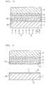
- Step 1As shown in Fig. 17, a separation layer (optical absorption layer) is formed on a substrate 100. The substrate 100 and the separation layer 120 will be described.
- the separation layer 120absorbs the incident light to cause internal and/or interfacial exfoliation, and preferably is composed of a material in which inter-atomic or inter-molecular adhering forces are reduced or eliminated by light irradiation to cause internal and/or interfacial exfoliation based on ablation.
- gas causing exfoliating effectsmay be released from the separation layer 120 by light irradiation in some cases, that is, a case in which components contained in the separation layer 120 are released as gas, and a case in which the separation layer 120 is instantaneously gasified by absorbing the incident light and the released vapor contributes to exfoliation.
- the composition of such a separation layer 120is similar to that in the first embodiment.
- a transferred layer (thin film device layer) 140is formed on the separation layer 120.
- An enlarged cross-sectional view of the portion K (surrounded by a dotted line in Fig. 18) of the thin film device layer 140is shown in the right side of Fig. 18.
- the thin film device layer 140is composed of a TFT (thin film transistor) formed on a SiO 2 film (interlayer) 142, and the TFT includes source and drain layers 146 composed of an n-doped polycrystalline silicon layer, a channel layer 144, a gate insulating film 148, a gate electrode 150, an insulating interlayer 154, and an electrode composed of, for example, aluminum.
- TFTthin film transistor
- the interlayer adjoining the separation layer 120is composed of a SiO 2 film, it may be composed of any other insulating film, such as Si 3 N 4 .
- the thickness of the SiO 2 film (interlayer)is adequately determined based on the purpose for the formation and its functions, and ranges generally from approximately 10 nm to 5 ⁇ m, and preferably 40 nm to 1 ⁇ m.
- the interlayeris formed for various purposes, and functions as at least one of a protective layer physically or chemically protecting the transferred layer 140, an insulating layer, a conductive layer, a shading layer to laser light, a barrier layer for preventing migration, and a reflection layer.
- the transferred layer (thin film device layer) 140may be directly formed on the separation layer 120, by omitting the formation of the interlayer, such as the SiO 2 film.
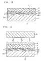
- the transferred layer (thin film device layer) 140includes a thin film device such as a TFT, as shown in the right side of Fig. 18. As well as a TFT, other thin film devices shown in the first embodiment can also be used. These thin film devices are generally formed at a relatively high process temperature inherent to the formation method. Thus, as described above, the substrate 100 must have high reliability and must be resistant to the process temperature. [Step 3] As shown in Fig. 19, the thin film device layer 140 is adhered to a transfer member 180 using an adhesive layer 160. Preferable examples of adhesives forming the adhesive layer 160 are described in the first embodiment.
- the curable adhesiveWhen using a curable adhesive, for example, the curable adhesive is applied onto the transferred layer (thin film device layer) 140, the transfer member 180 is adhered thereto, the curable adhesive is cured by a curing method in response to the property to adhere the transferred layer (thin film device layer) 140 with the transfer member 180.
- a photo-setting adhesivethe outer surface of the transparent substrate 100 or transparent transfer member 180 (or both outer surfaces of the transparent substrate and transparent transfer member) is irradiated with light.
- a photo-setting adhesivewhich barely affects the thin film device layer, is preferably used as the adhesive.
- the adhesive layer 160may be formed on the transfer member 180 and the transferred layer (thin film device layer) 140 may be adhered thereto.
- the formation of the adhesive layer 160can be omitted when the transfer member 180 has adhesive characteristics.
- Step 4As shown in Fig. 20, the rear side of the substrate 100 is irradiated with light. The light passing through the substrate 100 is incident on the separation layer 120. As a result, internal and/or interfacial exfoliation, which reduces or eliminates the adhering forces, occurs. It is presumed from the occurrence of the internal and/or interfacial exfoliation in the separation layer 120 that ablation of the constituents in the separation layer 120 occurs, that gas retained in the separation layer 120 is released, and that phase transition such as melting or vaporization occurs immediately after the light irradiation.
- ablationhas the same meaning as in the first embodiment.
- the incident lightis identical to the light used in the first embodiment.
- excimer lasersare preferably used.
- the excimer lasersoutput high energy laser beams in a shorter wavelength range which cause ablation in the separation layer 120 within a significantly shorter time.
- the separation layer 120is therefore cleaved substantially without the temperature rise, and thus without deterioration or damage of the adjacent or adjoining transfer member 180, and substrate 100.
- the wavelength of the incident laser beambe approximately 100 nm to 350 nm.
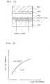
- Fig. 23is a graph of transmittance vs. wavelength of light in the substrate 100. As shown in the graph, the transmittance increases steeply at a wavelength of 300 nm.
- light beams having a wavelength of higher than 300 nmfor example, Xe-Cl excimer laser beams having a wavelength of 308 nm
- the wavelength of the incident laser beambe approximately 350 nm to 1,200 nm.
- the energy density of the incident laser light beam, and particularly of the excimer laser light beam,is similar to that in the first embodiment.
- a metallic film 124composed of tantalum (Ta) etc. may be formed on the separation layer (laser absorption layer) 120.
- the laser light passing through the separation layer 120is completely reflected on the interface with the metallic film 124, and thus does not affect the thin film device provided on the metallic film.
- the intensity of the incident lightsuch as laser light be uniform.
- the direction of the incident lightis not always perpendicular to the separation layer 120, and may be shifted by a given angle from the perpendicular direction.
- the entire region of the separation layer 120may be irradiated two or more times at the same position.
- the same position or different positionsmay be irradiated with different types or different wavelengths (wavelength regions) of the incident light (laser light).
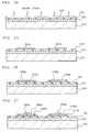
- the substrate 100is detached from the separation layer 120 by applying a force to the substrate 100.
- a part of the separation layermay remain on the substrate after the detachment, not shown in Fig. 21.
- the residual separation layer 120is removed by etching, ashing, washing, polishing or a combination thereof.
- the transferred layer (thin film device layer) 140is thereby transferred onto the transfer member 180.
- the moiety of the separation layer remaining on the substrate 100is removed.
- the substrate 100is composed of an expensive or rare material such as quartz glass, it is preferably reused (recycled). That is, the present invention is applicable to the substrate 100 to be reused, and is useful.
- the transfer of the transferred layer (thin film device layer) 140 onto the transfer member 180is completed by these steps.
- the SiO 2 film adjoining the transferred layer (thin film device layer) 140may be removed, or a conductive layer for wiring and/or a protective film may be formed on the transferred layer 140.
- the transferred layer (thin film device layer) 140is not directly separated as the detached member, but the separation layer adhered to the transferred layer (thin film device layer) 140 is exfoliated, hence uniform exfoliation or transfer is easily, securely, and uniformly achieved regardless of characteristics and conditions of the detached member (transferred layer 140). Since the detached member (transferred layer 140) is not damaged during the exfoliating operation, it can maintain high reliability.
- Examples 1 to 19 in the first embodimentcan also be applied to the third embodiment.
- the fourth embodimentincludes a modification of a step in the third embodiment.
- the separation layer 120is composed of amorphous silicon (a-Si), it is preferably formed by a chemical vapor deposition (CVD) process, and particularly by a low pressure (LP) CVD process, compared with plasma CVD, atmospheric pressure (AP) CVD, and ECR processes.
- CVDchemical vapor deposition
- LPlow pressure
- ECRatmospheric pressure
- an amorphous silicon layer formed by the plasma CVD processcontains a relatively large quantity of hydrogen.
- the presence of hydrogenmakes the ablation of the amorphous silicon layer easy, wherein hydrogen is released from the amorphous silicon layer at a temperature of higher than 350 °C.
- the evolution of hydrogen during the step forming the thin film devicemay cause exfoliation of the film.
- the plasma CVD filmhas relatively low adhesiveness, hence the substrate 100 may be detached from the transferred layer 140 in the wet washing step in the production of the device.
- the LPCVD filmhas no possibility of evolution of hydrogen and has sufficient adhesiveness.
- the thickness of the amorphous silicon layer 120 as the separation layerwill be described with reference to Fig. 39.
- the horizontal axisrepresents the thickness of the amorphous silicon layer
- the vertical axisrepresents the optical energy absorbed in this layer.
- ablationmeans that solid components (the constituents of the separation layer 120), which absorbed the incident light, are photochemically and thermally excited and atoms and molecules in the solid components are released by the chain scission.
- the ablationis observed as phase transition such as melting or vaporization in the partial or entire constituents of the separation layer 120.
- fine foamingmay be formed by the phase change, resulting in a decreased adhering force.
- the absorbed energy required for the ablationdecreases with a decreased thickness, as shown in Fig. 39.
- the thickness of the amorphous silicon layer 120 as the separation layeris reduced in this embodiment.
- the energy of the light incident on the amorphous silicon layer 120is thereby reduced, resulting in lower energy consumption and miniaturization of the light source unit.
- the thickness level of the amorphous silicon layer 120 as the separation layerwill now be investigated. As shown in Fig. 39, the absorbed energy required for the ablation decreases as the thickness of amorphous silicon decreases. According to the present inventors investigation, it is preferable that the thickness be 25 nm or less, hence ablation can occur by the power of a general light source unit.
- the lower limit of the thicknessis not limited, a lower limit of 5 nm may be determined in view of the secure formation and adhesiveness of the amorphous silicon layer. Accordingly, the preferable thickness of the amorphous silicon layer 120 ranges from 5 nm to 25 nm, and more preferably 15 nm or less for achieving further energy saving and higher adhesiveness. The optimum range of the thickness is 11 nm or less, and the absorbed energy required for the ablation can be significantly decreased near that thickness.
- the fifth embodimentincludes a modification of a step in the third or fourth embodiment.
- the transfer member 180has preferably a certain amount of rigidity as a mechanical property, it may have flexibility or elasticity. Such a mechanical property of the transfer member 180 is determined in consideration of the following point.
- the constituent material of the separation layer 120is photochemically or thermally excited, and molecules or atoms on and in the layer are cleaved to release molecules or atoms outside.
- the transfer member 180has mechanical strength which is resistant to the stress acting on the upper portion of the separation layer 120 accompanied by the release of molecules or atoms. A deformation or breakage at the upper portion of the separation layer 120 can be thereby prevented.
- Such mechanical strengthmay be imparted not only to the transfer member 180, but also to at least one layer lying above the separation layer 120, that is, the transferred layer 140, the adhesive layer 160, and the transfer member 180.
- the materials for and thicknesses of the transferred layer 140, adhesive layer 160, and transfer member 180can be determined in order to achieve such mechanical strength.
- a reinforcing layer 132may be formed at an appropriate position above the separation layer 120, as shown in Figs. 42(A) to 42(E).
- the reinforcing layer 132 shown in Fig. 42 (A)is provided between the separation layer 120 and the transferred layer 140. After forming exfoliation in the separation layer 120 and detaching the substrate 100, the reinforcing layer 132 can be removed together with the remaining separation layer 120 from the transferred layer 140. As shown in Fig. 42(B), the reinforcing layer 132 provided above the transferred layer 180 can also be removed from the transferred layer 180, after the separation layer 120 is cleaved.
- the reinforcing layer 132 shown in Fig. 42 (C)intervenes as, for example, an insulating layer in the transferred layer 140 composed of a plurality of layers. Each reinforcing layer 132 shown in Figs. 42(D) and 42(E) is placed under or on the adhesive layer 160. In such a case, it cannot be removed later.
- the sixth embodimentincludes a modification of a step in any one of the third, fourth, and fifth embodiments.
- a method shown in Fig. 40 or 41be employed instead of the method shown in Fig. 38.
- an amorphous silicon layer 120is employed as the separation layer, and another amorphous silicon layer 126 is also employed as a silicon-based optical absorption layer.
- a silicon oxide (SiO 2 ) filmintervenes as a silicon-based intervening layer. Even if the incident light passes through the amorphous silicon layer 120 as the separation layer, the transmitted light is absorbed in the amorphous silicon layer 126 as the silicon-based optical absorption layer. As a result, the thin film device provided thereon is not adversely affected. Since the two additional layers 126 and 128 are composed of silicon, metallic contamination etc. does not when using an established conventional film deposition technology.
- the thickness of the amorphous silicon layer 120 as the separation layeris larger than the thickness of the amorphous silicon layer 126 as the optical absorption layer, exfoliation in the amorphous silicon layer 126 can be securely prevented. Regardless of such a relationship of the thicknesses, however, the optical energy incident on the amorphous silicon layer 126 is considerably lower than the optical energy incident on the amorphous silicon layer 120 as the separation layer, no ablation occurs in the amorphous silicon layer 126.
- Fig. 41shows a case providing a silicon-based optical absorption layer 130 composed of a different material from that of the separation layer 120, wherein the silicon-based intervening layer is not always necessary.
- the seventh embodimentincludes a modification of a step in any one of the third to sixth embodiments.
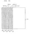
- Figs. 43 and 44show a method for irradiating almost the entire separation layer 120 with light.
- the number of scanning times of line beamsis represented by N, and beam scanning is performed such that the region 20(N) irradiated with the N-th line beam 10 does not overlap with the region 20(N+1) irradiated with the (N+1)-th line beam 10.
- a low- or non-irradiation region 30which is significantly narrower than each irradiated region is formed between the two adjacent regions 20(N) and 20(N+1).
- a low-irradiation region 30is formed.
- a non-irradiation region 30is formed.
- the separation layer 120is irradiated with an excessive amount of incident light which is larger than that required for internal and/or interfacial exfoliation.
- the light leaked from the separation layer 120is incident on the transferred layer 140 including a thin film device, electrical and other characteristics of the thin film device will deteriorate.
- the separation layer 120is not irradiated with such excessive light, hence the original characteristics inherent to the thin film device can be maintained after the it is transferred onto the transfer member.
- exfoliatingdoes not occur in the low- or non-irradiation region 30 in the separation layer 120, the adhesiveness between the separation layer 120 and the substrate 100 can be satisfactorily reduced by exfoliating in the regions irradiated with the line beams.
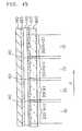
- Fig. 44beam scanning is performed such that the region 20(N) irradiated with the N-th line beam 10 overlaps with the region 20 (N+1) irradiated with the (N+1)-th line beam 10.
- a doubly-irradiated region 40is therefore formed between the two adjacent regions 20(N) and 20(N+1).
- Figs. 46 and 47are graphs of distributions of optical intensity vs. the position of the two adjacent line beams 10 and 10 in beam scanning.
- each line beam 10has a flat peak 10a having a maximum intensity at a predetermined region including the beam center.
- the two adjacent line beams 10 and 10are scanned such that the two corresponding flat peaks 10a do not overlap with each other.
- each line beam 10has a beam center with a maximum intensity, wherein the optical intensity decreases at a point distant from the beam center.
- the two adjacent line beams 10 and 10are scanned such that the two beam-effective regions having an intensity which is 90% of the maximum intensity of each line beam 10 do not overlap with each other.
- the total dose (summation of products of optical intensities by irradiated times at each position) of the light beams incident on the doubly-irradiated region 40is lower than that of the flat region or beam-effective region.
- the doubly-irradiated region 40therefore, will first be cleaved at the second irradiation of the beams, and this does not correspond to the excessive irradiation of beam. If the relevant region of the separation layer is cleaved at the first irradiation, the intensity in the second irradiation of the light beam, which is incident on the thin film device, is reduced, hence deterioration of the electrical characteristics of the thin film device can be prevented or significantly reduced to a practical level.
- the intensity of each beam which is incident on the doubly-irradiated region 40be less than 90%, more preferably 80% or less, and most preferably 50% or less of the maximum intensity at the center of each beam.
- the intensity of the beamis significantly high so that exfoliation occurs at an intensity which is half (50%) the maximum intensity of the beam, overlapping at regions in which the intensity is higher than half of the maximum intensity may be avoided.
- Such irradiation modescan also be applicable to beam shapes, such as a spot beam, other than a line beam.
- beam shapessuch as a spot beam, other than a line beam.
- spot beam scanningvertical and horizontal relationships between the adjacent irradiated regions must be taken into account.
- the direction of the incident light including laser lightis not limited to the direction perpendicular to the separation layer 120, and may be shifted by a given angle from the perpendicular direction as long as the intensity of the incident light is substantially uniform in the separation layer 120.
- Example 1 of the third embodimentcorresponds to a modification of the laser irradiation in Example 1 of the third embodiment.
- a quartz substrate with a length of 50 mm, a width of 50 mm, and a thickness of 1.1 mm (softening point: 1,630 °C, distortion point: 1,070 °C, and transmittance of excimer laser: approximately 100%)was prepared, and an amorphous silicon (a-Si) film as a separation layer (laser-absorption layer) was formed on the one side of the quartz substrate by a low pressure CVD process (Si 2 H 6 gas, 425 °C).
- the thickness of the separation layerwas 100 nm.
- a SiO 2 film as an interlayerwas formed on the separation layer by an ECR-CVD process (SiH 4 +O 2 gas, 100 °C).
- the thickness of the interlayerwas 200 nm.
- a polycrystalline silicon (or polycrystalline silicon) film with a thickness of 50 nm as a transferred layerwas formed on the interlayer by a CVD process (Si 2 H 6 gas).
- the polycrystalline silicon filmwas patterned to form source/drain/channel regions of a thin film transistor.
- a SiO 2 gate insulating filmwas formed by thermal oxidation of the surface of the polycrystalline silicon film, a gate electrode (a structure in which a high melting point metal, such as Mo, was deposited on the polycrystalline silicon) was formed on the gate insulating film, and source and drain regions were formed by self alignment by means of ion implantation using the gate electrode as a mask.
- a thin film transistorwas thereby formed.
- a thin film transistor having similar characteristicscan be formed by a low temperature process instead of such a high temperature process.
- an amorphous silicon film with a thickness of 50 nm as a transferred layerwas formed on a SiO 2 film as an interlayer on the separation layer by a low pressure CVD process (Si 2 H 6 gas, 425 °C), and the amorphous silicon film was irradiated with laser beams (wavelength: 308 nm) to modify the amorphous silicon into a polycrystalline silicon film by crystallization.
- the polycrystalline silicon filmwas patterned to form source/drain/channel regions having a given pattern of a thin film transistor.
- a gate electrode(a structure in which a high melting point metal, such as Mo, was deposited on the polycrystalline silicon) was formed on the gate insulating film, and source and drain regions were formed by self alignment by means of ion implantation using the gate electrode as a mask. A thin film transistor was thereby formed.
- electrodes and leads connected to the source and drain regions and leads connected to the gate electrodewere formed, if necessary.
- These electrodes and leadsare generally composed of aluminum, but not for the limitation.
- a metal(not melted by laser irradiation in the succeeding step) having a melting point higher than that of aluminum may be used if melting of aluminum is expected in the succeeding laser irradiation step.
- a UV-curable adhesive(thickness: 100 ⁇ m) was applied onto the thin film transistor, a large, transparent glass substrate (soda glass, softening point: 740 °C, distortion point: 511 °C) as a transfer member was adhered to the adhesive film, and the outer surface of the glass substrate was irradiated with ultraviolet rays to fix these layers by curing the adhesive.
- the surface of the quartz substratewas irradiated with Xe-Cl excimer laser beams (wavelength: 308 nm) to cause exfoliation (internal and interfacial exfoliation) of the separation layer.
- the energy density of the Xe-Cl excimer laserwas 250 mJ/cm 2 , and the irradiation time was 20 nano seconds.
- the excimer laser irradiation methodsinclude a spot-beam irradiation method and a line-beam irradiation method.
- a given unit areafor example 8 mm by 8 mm
- the spot irradiationis repeated while scanning the spot beam such that irradiated regions do not overlap with each other (in the vertical and horizontal directions), as shown in Fig. 43.
- a given unit areafor example 378 mm ⁇ 0.1 mm, or 378 mm ⁇ 0.3 mm (absorbing 90% or more of the incident energy)
- irradiationmay be performed such that the total intensity of the beams is reduced in the doubly-irradiated region.
- the quartz substratewas detached from the glass substrate (transfer member) at the separation layer, so that the thin film transistor and interlayer formed on the quartz substrate were transferred onto the glass substrate.
- the separation layer remaining on the interlayer on the glass substratewas removed by etching, washing, or a combination thereof. A similar process was applied to the quartz substrate for recycling it.
- the transfer from the quartz substrate to the glass substrate in accordance with this examplecan be repeated to form a number of thin film transistors on different positions on the quartz substrate.
- a larger number of thin film transistorscan be formed on the glass substrate by repeated deposition cycles.
- the exfoliation member or transferred layer in any one of the first to seventh embodimentsis composed of a CMOS-TFT.
- Figs. 24 to 34are cross-sectional views of the steps in the exfoliating method in this embodiment.
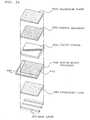
- a CPU 300provided with a circuit including thin film devices, a RAM 320, an input-output circuit 360, and a solar battery 340 having PIN-junction of amorphous silicon for supplying electrical power to these circuits are mounted. Since the microcomputer in Fig. 35(a) is formed on the flexible substrate, it is resistive to bending, as shown in Fig. 35(b), and to dropping because of its light weight.
- An active matrix liquid crystal display deviceshown in Figs. 36 and 37, using an active matrix substrate can be produced by a transfer technology of any one of the first to fourth embodiments.
- the active matrix liquid crystal display deviceis provided with an illumination source 400 such as a back light, a polarizing plate 420, an active matrix substrate 440, a liquid crystal 460, a counter substrate 480, and a polarizing plate 500.
- an illumination source 400such as a back light
- a polarizing plate 420an active matrix substrate 440
- a liquid crystal 460a liquid crystal 460
- a counter substrate 480a polarizing plate 500.
- a flexible, lightweight active matrix liquid crystal panel resistant to impactcan be achieved by substituting a reflecting liquid crystal panel using a reflective plate instead of the illumination source 400.
- the pixel electrodeis formed of metal, the reflecting plate and the polarizing plate 420 are not required.
- the active matrix substrate 440 used in this embodimentis a driver-built-in active matrix substrate in which a TFT is provided in a pixel section 442 and a driver circuit (a scanning line driver and a data line driver) 444 is built in.
- a circuit of a main section of the active matrix liquid crystal display deviceis shown in Fig. 37.
- a gateis connected to a gate line G1, and either a source or a drain is connected to a data line D1.
- the pixel section 442includes a TFT (M1) and a liquid crystal 460, wherein the other of the source and drain is connected to the liquid crystal 460.
- a driver section 444includes a TFT (M2) formed by the same process as for the TFT (M1) in the pixel section 442.
- the active matrix substrate 440 including TFTs (M1 and M2)can be formed by the transferring method in accordance with either the third or fourth embodiment.
- exfoliation memberscapable of forming on substrates are transferred onto transfer members which are other than the substrates which are used in the formation of the exfoliation members so that the exfoliation members are arranged on the transfer members which are other than the substrates used in the formation of the exfoliation members. Accordingly, the present invention is applicable to production of various devices including liquid crystal devices and semiconductor integrated circuits.
Landscapes
- Physics & Mathematics (AREA)
- Engineering & Computer Science (AREA)
- General Physics & Mathematics (AREA)
- Microelectronics & Electronic Packaging (AREA)
- Condensed Matter Physics & Semiconductors (AREA)
- Manufacturing & Machinery (AREA)
- Computer Hardware Design (AREA)
- Power Engineering (AREA)
- Nonlinear Science (AREA)
- Mathematical Physics (AREA)
- Crystallography & Structural Chemistry (AREA)
- Chemical & Material Sciences (AREA)
- Optics & Photonics (AREA)
- Thin Film Transistor (AREA)
- Liquid Crystal (AREA)
- Electroluminescent Light Sources (AREA)
Abstract
Description
- The present invention relates to a method for exfoliating a detached member, and in particular, a transferring method for exfoliating a transferred layer comprising a thin film such as a functional thin film and for transferring it onto a transfer member such as a transparent substrate. Also, the present invention relates to a transferring method of a thin film device, a thin film device, a thin film integrated circuit device, and a liquid crystal display device produced using the same.
- Production of liquid crystal displays using thin film transistors (TFTs), for example, includes a step for forming thin film transistors on a transparent substrate by a CVD process or the like.
- The thin film transistors are classified into those using amorphous silicon (a-Si) and those using polycrystalline silicon (p-Si), and those using polycrystalline silicon are classified into those formed by a high temperature process and those formed by a low temperature process.
- Since the formation of such thin film transistors on a substrate involves treatment at a relatively high temperature, a heat resistant material, that is, a material having a high softening point and a high melting point must be used as the transparent substrate. At present, in the production of TFTs by high temperature processes, transparent substrates composed of quartz glass which are sufficiently resistive to a temperature of approximately 1,000 °C are used. When TFTs are produced by low temperature processes, the maximum process temperature is near 500 °C, hence heat-resisting glass which is resistive to a temperature near 500 °C is used.
- As described above, a substrate for use in forming thin film devices must satisfy the conditions for producing these thin film devices. The above-mentioned "substrate" is, however, not always preferable in view of the steps after fabrication of the thin film devices on the substrate is completed.
- For example, in the production process with high temperature treatment, quartz glass or heat-resisting glass is used, however, they are rare and very expensive materials, and a large transparent substrate can barely be produced from the material.
- Further, quartz glass and heat-resisting glass are fragile, easily broken, and heavy. These are severe disadvantages when a substrate provided with thin film devices such as TFTs is mounted into electronic units. There is a gap between restriction due to process conditions and preferred characteristics required for products. Hence it is significantly difficult to satisfy both the restriction and preferred characteristics.
- The present invention has been achieved in view of such a problem, and has an object to provide an exfoliating method, which permits easy exfoliation regardless of characteristics of the detached member and conditions for exfoliating, and transferring to various transfer members. Another object is to provide a novel technology which is capable of independently selecting a substrate used in production of thin film devices and a substrate suited to the use of the product (a substrate having preferable properties for use of the product). A further object is to provide a novel technology not causing deterioration of characteristics of thin film devices which are transferred onto a substrate, by decreasing the optical energy radiated to the separable layer causing ablation in the transferring process.
- 1. First, a method for exfoliating a detached member or a transferred layer from a substrate for production is disclosed. The inventions are as follows:
- (1) An exfoliating method in accordance with the present invention is a method for exfoliating a detached member, which is present on a substrate with a separation layer therebetween, from the substrate, wherein the separation layer is irradiated with incident light so as to cause exfoliation in the separation layer and/or at the interface, and to detach the detached member from the substrate.
- (2) A method for exfoliating a detached member, which is present on a transparent substrate with a separation layer therebetween, from the substrate, wherein the separation layer is irradiated with incident light from the side of the substrate so as to cause exfoliation in the separation layer and/or at the interface, and to detach the detached member from the substrate.
- (3) A method for exfoliating a transferred layer formed on a substrate with a separation layer therebetween from the substrate and transferring the transferred layer onto a transfer member, wherein after the transfer member is adhered to the opposite side of the transferred layer to the substrate, the separation layer is irradiated with incident light so as to cause exfoliation in the separation layer and/or at the interface, and to detach the transferred layer from the substrate to transfer onto the transfer member.
- (4) A method for exfoliating a transferred layer formed on a transparent substrate with a separation layer therebetween from the substrate and transferring the transferred layer onto a transfer member, wherein after the transfer member is adhered to the opposite side of the transferred layer to the substrate, the separation layer is irradiated with incident light from the side of the substrate so as to cause exfoliation in the separation layer and/or at the interface, and to detach the transferred layer from the substrate to transfer onto the transfer member.
- (5) An exfoliating method includes a step for forming a separation layer on a transparent substrate, a step for forming a transferred layer on the separation layer directly or with a given interlayer therebetween, a step for adhering the transfer member to the opposite side of the transferred layer to the substrate, and a step for irradiating the separation layer with incident light from the side of the substrate so as to cause exfoliation in the separation layer and/or at the interface, and to detach the transferred layer from the substrate to transfer onto the transfer member.
After transferring the transferred layer onto the transfer member, a step for removing the separation layer adhering to the side of the substrate and/or transfer member may be provided.
A functional thin film or a thin film device may be used as the transferred layer. Particularly, a thin film transistor is preferably used as the transferred layer. Preferably, the transfer member is a transparent substrate.
When the maximum temperature in the formation of the transferred layer is Tmax, it is preferred that the transfer member be composed of a material having a glass transition point (Tg) or softening point which is lower than Tmax. Particularly, it is preferred that the transfer member be composed of a material having a glass transition point (Tg) or softening point which is lower than 800 °C.
It is preferable that the transfer member be composed of a synthetic resin or glass.
It is preferable that the substrate has thermal resistance. In particular, when the maximum temperature in the formation of the transferred layer is Tmax, it is preferred that the substrate be composed of a material having a distortion point which is lower than Tmax.
In the above-mentioned exfoliating methods, the exfoliation of the separation layer is caused by an elimination of or a decrease in the adhering force between atoms or molecules in the constituent substances in the separation layer.
It is preferable that the incident light be laser light. Preferably, the laser light has a wavelength of 100 nm to 350 nm. Alternatively, the laser light has a wavelength of 350 nm to 1,200 nm.
It is preferable that the separation layer is composed of amorphous silicon. Preferably, the amorphous silicon contains 2 atomic percent or more of hydrogen (H).
The separation layer may be composed of a ceramic. Alternatively, the separation layer may be composed of a metal. Alternatively, the separation layer may be composed of an organic polymer. In this case, it is preferable that the organic polymer has at least one adhere selected from the group consisting of -CH2-, -CO-, -CONH-, -NH-, -COO-, -N=N-, and -CH=N-. Further, it is preferable that the organic polymer has an aromatic hydrocarbon group in the chemical formula. - 2. Next, inventions in which the above-mentioned separation layer includes a plurality of composites are disclosed. These inventions are as follows.
First, the separation layer in the inventions disclosed inparagraph 1 includes a composite with a plurality of layers. Further, the separation layer includes at least two layers having different compositions or characteristics.
It is preferable that the separation layer includes an optical absorption layer for absorbing the incident light and another layer having a different composition or property from the optical absorption layer. Preferably, the separation layer includes the optical absorption layer for absorbing the incident light and a shading layer for shading the incident light. Preferably, the shading layer lies at the opposite side of the optical absorption layer to the incident light. Preferably, the shading layer is a reflection layer for reflecting the incident light. Preferably, the reflection layer is composed of a metallic thin film. - 3. A method for transferring a thin film device, which is used as a detached member or a transferred member, will now be disclosed.
A method for transferring a thin film device on a substrate onto a transferred member includes: a step for forming a separation layer on the substrate; a step for forming a transferred layer including the thin film device onto the separation layer; a step for adhering the transferred layer including the thin film device to the transfer member with an adhesive layer, a step for irradiating the separation layer with light so as to cause exfoliation in the separation layer and/or at the interface; and a step for detaching the substrate from the separation layer.
In accordance with the present invention, for example, a separation layer having optical absorption characteristics is provided on a substrate having high reliability in device production, and thin film devices such as TFTs and the like are formed on the substrate. Next, although not for limitation, the thin film devices are adhered to a given transfer member, for example, with an adhesive layer, so as to cause an exfoliation phenomenon in the separation layer, which results in a decrease in adhering between the separation layer and the substrate. The substrate is detached from the thin filmdevices by the force applied to the substrate. A given device with high reliability can be thereby transferred or formed onto any transfer members.
In the present invention, either the step for adhering the thin film devices (the transferred layer including the thin film devices) to the transfer member with the adhesive layer or the step for detaching the substrate from the thin film devices may precede. When handling of the thin film devices (the transferred layer including the thin film devices) after detaching the substrate is troublesome, however, it is preferable that the thin film devices be adhered to the transfer member, and then the substrate be detached.
When an adhesive layer for adhering the thin film devices to the transfer member is, for example, a substance having planation, the uneven face formed on the surface of the transferred layer including the thin film devices is negligible by the planation, the adhering to the transfer member is satisfactorily performed. The substrate may be a transparent substrate, and thus the separation layer is irradiated with the light through the transparent substrate. The use of, for example, a transparent substrate, e.g. a quartz substrate, permits production of thin film devices with high reliability and collective irradiation of the entire separation layer with the light from the rear side of the substrate, resulting in an improvement in the transfer efficiency. - 4. Inventions in which parts of the steps, disclosed in the above-mentioned
paragraph 3, in the method for transferring the thin film device will now be disclosed. These inventions are as follows:- (1) A method for transferring a transferred layer including a thin film device forming on a substrate onto a transfer member comprising: a first step for forming an amorphous silicon layer on the substrate; a second step for forming the transferred layer including the thin film device on the amorphous silicon layer; a third step for adhering the transferred layer including the thin film device to the transfer member with an adhesive layer; a fourth step for irradiating the amorphous silicon layer with light through the substrate so as to cause exfoliation in the amorphous silicon layer and/or at the interface and to decrease the adhering force between the substrate and the transferred layer; and a fifth step for detaching the substrate from the amorphous silicon layer; wherein the transferred layer formed in the second step includes a thin film transistor, and the thickness of the amorphous silicon layer formed in the first step is smaller than the thickness of the channel layer of the thin film transistor formed in the second step.
In this invention, the amorphous silicon layer is used as the layer formed on the substrate in the first step and causes exfoliation by light irradiation. In the amorphous silicon layer as shown in Fig. 39, optical energy, which is radiated in the amorphous silicon layer and which is required for exfoliation (referred to as ablation in Fig. 39), decreases as the thickness decreases.
The transferred layer formed in the second step includes the thin film transistor as a thin film device, its channel layer is formed of silicon, e.g., polycrystalline silicon or amorphous silicon, and the transferred layer has a thickness of more than 25 nm, for example, approximately 50 nm. In this invention, the thickness of the amorphous silicon as the separation layer (ablation layer) formed in the first step is smaller than that of the channel layer of the thin film transistor in the transferred layer. The energy consumed in the light irradiation step therefore decreases, and the light source can be miniaturized. Further, since optical energy by irradiation is low, the deterioration of the thin film device is suppressed if the light leaked from the amorphous silicon layer is incident on the thin film device.
Now, the thickness of the amorphous silicon layer is set to 25 nm or less. As described above, the optical energy, which is radiated in the amorphous silicon layer and which is required for exfoliation, decreases as the thickness decreases, hence the optical energy is significantly low at this thickness. It is preferable that the thickness of the amorphous silicon layer be in a range from 5 nm to 25 nm, more preferably 15 nm or less, and most preferably 11 nm or less in order to further decrease the optical energy, which is radiated in the amorphous silicon layer and which is required for exfoliation.
In the second step, the amorphous silicon layer is formed by a low pressure chemical vapor deposition (LPCVD) process. The amorphous silicon layer formed by the LPCVD process has a higher adhesion compared with a plasma CVD process, an atmospheric pressure (AP) CVD process, or an ECR process, hence there is not much risk of failures, such as evolution of hydrogen and flaking of the film, during the formation of the transferred layer including the thin film device. - (2) A method for transferring a transferred layer including a thin film device on a substrate onto a transfer member comprising: a step for forming a separation layer onto the substrate; a step for forming a silicon-based optical absorption layer on the separation layer; a step for forming the transferred layer including the thin film device on the silicon-based optical absorption layer; a step for adhering the transferred layer including the thin film device to the transfer member with an adhesive layer; a step for irradiating the separation layer with light through the substrate so as to cause exfoliation in the separation layer and/or at the interface; and a step for detaching the substrate from the separation layer.
In accordance with this invention, if light leaks from the separation layer, the leaked light is absorbed in the silicon-based optical absorption layer before it is incident on the thin film device. No light is therefore incident on the thin film device, hence the thin film device is prevented from characteristic deterioration due to the incident light. The transferred layer including the thin film device can be formed on the silicon-based optical absorption layer. Metallic contamination will therefore not occur as in the case forming the transferred layer onto a metallic layer reflecting light, and the thin film device can be formed by an established thin film deposition technology.
The separation layer and the optical absorption layer are formed of amorphous silicon, and a step for providing a silicon-based intervening layer between the separation layer and the optical absorption layer. As shown in Fig. 39, the amorphous silicon layer, which absorbs the incident light and separates when the energy of the absorbed light reaches a given value, is used as the separation layer and the silicon-based optical absorption layer. As the intervening layer for separating the two amorphous silicon layers, a silicon compound, for example, silicon oxide, is used. - (3) A method for transferring a transferred layer including a thin film device on a substrate onto a transfer member comprising: a first step for forming a separation layer on the substrate; a second step for forming the transferred layer including the thin film device on the separation layer; a third step for adhering the transferred layer including the thin film device to the transfer member with an adhesive layer; a fourth step for irradiating the separation layer with light through the substrate so as to cause exfoliation in the separation layer and/or at the interface; and a fifth step for detaching the substrate from the separation layer; wherein, in the fourth step, the stress, acting on the upper layers above the separation layer in the exfoliation in the separation layer and/or at the interface, is absorbed by the proof stress of the upper layers above the separation layer to prevent the deformation or breakage of the upper layers above the separation layer.
In the fourth step, the substances in the separation layer are optically or thermally excited by the incident light to cut bonds of atoms or molecules on the surface and in the interior and liberate the molecules and atoms to the exterior. This phenomenon is observed as phase transition, such as melting or evaporation, of the partial or entire substances in the separation layer. A stress acts on the upper layers above the separation layer as the molecules or atoms are released. The stress is, however, absorbed by the proof stress of the upper layers above the separation layer so as to prevent deformation or breakage of the upper layers above the separation layer.
The materials and/or thicknesses of the upper layers above the separation layer may be designed in view of such a proof stress. For example, one or more among the thickness of the adhesive layer, the thickness of the transferred layer, the material, and the thickness of the transfer member is designed in view of the proof stress.
Before performing the fourth step, the method further includes a step for forming a reinforcing layer for ensuring the proof stress at any position among the upper layers above the separation layer. In this invention, if the proof stress is not ensured only by the minimum configuration of the upper layers above the separation layer, consisting of the adhesive layer, the transferred layer, and the transfer member, deformation and breakage of the thin film device is prevented by adding the reinforcing layer. - (4) A method for transferring a transferred layer including a thin film device on a substrate onto a transfer member comprising: a first step for forming a separation layer on the substrate; a second step for forming the transferred layer including the thin film device on the separation layer; a third step for adhering the transferred layer including the thin film device to the transfer member with an adhesive layer; a fourth step for irradiating the separation layer with light through the substrate so as to cause exfoliation in the separation layer and/or at the interface; and a fifth step for detaching the substrate from the separation layer; wherein, the fourth step includes sequential scanning of beams for locally irradiating the separation layer, such that a region irradiated by the N-th beam (wherein N is an integer of 1 or more) does not overlap with other irradiated regions.
In the present invention, the separation layer is irradiated with such an excessive amount of light, hence the original characteristics of the thin film device are maintained after the thin film device is transferred onto the transfer member. A zone between individual beam-irradiated regions may be a low irradiation zone in which light is incident during the relative movement or a non-irradiation zone in which no light is incident during the relative movement. Exfoliation does not occur in the low irradiation zone or non-irradiation zone, the adhesion between the separation layer and the substrate can be remarkably reduced.
In the following two inventions, each beam for preventing or suppressing the characteristic deterioration of the thin film device is determined in different views from the invention in paragraph (4).
In the fourth step of the first invention, beams are sequentially scanned to irradiate locally the separation layer, each beam has a flat peak region having the maximum optical intensity in the center, and a region irradiated by the N-th beam (wherein N is an integer of 1 or more) does not overlap with other irradiated regions.
In the fourth step of the other invention, beams are sequentially scanned to irradiate locally the separation layer, each beam has the maximum optical intensity in the central region, and an effective region irradiated by the N-th beam (wherein N is an integer of 1 or more) having an intensity, which is 90% or more of the maximum intensity, does not overlap with the other effective regions irradiated by other beam scanning.
Since individual beams are scanned so that the flat peaks of individual beams or the effective regions having intensities which are 90% or more of the maximum intensity do not overlap with each other, two beams are continuously scanned in the same region in the separation layer. The total irradiated beam (sum of the optical intensity × time) in the same region is lower than that when the flat peak region or the effective region having intensities which are 90% or more of the maximum intensity is set at the same position in the two consecutively scanned beams. As a result, the separation layer may separate after the second scanning in some regions, and this case does not correspond to the excessive irradiation. In another case, even if the separation layer separates in the first scanning, the intensity of the light incident on the thin film device in the second scanning is decreased, hence the deterioration of the electric characteristics of the thin film device can be prevented or reduced.
In the thin film device formed on a given substrate by a transfer technology of the thin film device (the thin film structure) in accordance with the present invention, the deterioration of various characteristics can be prevented or reduced by improving the irradiating step for exfoliating the separation layer.
When the thin film device is a thin film transistor (TFT), the improved irradiation step for exfoliating the separation layer can prevent the breakdown of the TFT due to a decreased on-current flow and an increased off-current flow in the channel layer of the TFT damaged by the incident light. - (1) A method for transferring a transferred layer including a thin film device forming on a substrate onto a transfer member comprising: a first step for forming an amorphous silicon layer on the substrate; a second step for forming the transferred layer including the thin film device on the amorphous silicon layer; a third step for adhering the transferred layer including the thin film device to the transfer member with an adhesive layer; a fourth step for irradiating the amorphous silicon layer with light through the substrate so as to cause exfoliation in the amorphous silicon layer and/or at the interface and to decrease the adhering force between the substrate and the transferred layer; and a fifth step for detaching the substrate from the amorphous silicon layer; wherein the transferred layer formed in the second step includes a thin film transistor, and the thickness of the amorphous silicon layer formed in the first step is smaller than the thickness of the channel layer of the thin film transistor formed in the second step.
- 5. Further, the following inventions are disclosed in connection with the above-mentioned inventions.
- A step for removing the separation layer adhered to the transfer member is provided for completely removing the unnecessary separation layer.
- The transfer member is a transparent substrate. For example, inexpensive substrates such as a soda glass substrate and flexible transparent plastic films may be used as the transfer member. When the maximum temperature of the transfer member during the formation is Tmax, the transfer member is composed of a material having a glass transition point (Tg) or softening point which is lower than Tmax.
- Although such inexpensive glass substrates etc. have not been used because they are not resistive to the maximum temperature of the conventional device production processes, they can be used in the present invention without restriction.
- The glass transition point (Tg) or softening point of the transfer member is lower than the maximum temperature in the process for forming the thin film device. The upper limit of the glass transition point (Tg) or softening point is defined. The transfer member is composed of a synthetic resin or a glass material. For example, when the thin film device is transferred onto a flexible synthetic resin plate such as a plastic film, excellent characteristics which are not obtainable in a glass substrate with high rigidity can be achieved. When the present invention is applied to a liquid crystal device, a flexible lightweight display device which is resistive to shock damage can be achieved.
- Also, a thin film integrated circuit such as a single-chip microcomputer including TFTs can be formed by transferring the TFTs on a synthetic resin substrate by the above-mentioned transferring method.
- An inexpensive substrate such as a soda-glass substrate can also be used as the transfer member. A soda-glass substrate is inexpensive and thus has economical advantages. Since alkaline components are dissolved from the soda-glass substrate during annealing of the TFT production, it has been difficult to apply active matrix liquid crystal display devices. In accordance with the present invention, however, since a completed thin film device is transferred, the above-mentioned problems caused by the annealing will not occur. Accordingly, substrates having problems in the prior art technologies, such as a soda-glass substrate, can be used in the field of active matrix liquid crystal display devices.
- The substrate has thermal resistivity: The thin film device can be annealed at a high temperature in the production process, and the resulting thin film device has high reliability and high performance.
- The substrate has a transmittance of 10% or more for the 310nm light: The transparent substrate can supply optical energy sufficient to ablation in the separation layer.
- When the maximum temperature in the formation of the transferred layer is Tmax, the substrate is composed of a material having a distortion point of Tmax or more: The thin film device can be treated at a high temperature in the production process, and the resulting thin film device has high reliability and high performance.
- The separation layer may be composed of amorphous silicon:
- The amorphous silicon can absorb light, can be easily produced, and has a highly practical use.
- The amorphous silicon contains 2 atomic percent or more of hydrogen (H): When the amorphous silicon containing hydrogen is used, hydrogen is released by light irradiation, and an internal pressure occurs in the separation layer to promote exfoliation in the separation layer. The amorphous silicon may contain 10 atomic percent or more of hydrogen (H). The exfoliation in the separation layer is further accelerated by the increased hydrogen content.
- Alternatively, the separation layer may be composed of silicon nitride: When using silicon nitride as a separation layer, nitrogen is released by light irradiation to promote exfoliation in the separation layer.
- Alternatively, the separation layer may be composed of a hydrogen-containing alloy: When using a hydrogen-containing alloy, hydrogen is released by light irradiation to promote exfoliation in the separation layer.
- Alternatively, the separation layer may be composed of a nitrogen-containing alloy: When using a nitrogen-containing alloy, nitrogen is released by light irradiation to promote exfoliation in the separation layer.
- The separation layer may be composed of a multi-layered film: The separation layer is therefore not limited to a single-layered film. The multi-layered film is composed of an amorphous silicon film and a metallic film formed thereon.
- The separation layer may be composed of at least one material selected from the group consisting of ceramics, metals, and organic polymers. Usable metals include, for example, hydrogen containing alloys and nitrogen containing alloys. As in amorphous silicon, exfoliation in the separation layer is accelerated by the evolution of gaseous hydrogen or nitrogen by light irradiation.
- The light is laser light. Laser light is coherent light and is suitable for causing exfoliation in the separation layer. The laser light has a wavelength of 100 nm to 350 nm. The short-wave, high energy laser light results in effective exfoliation in the separation layer. An example of such a laser is an excimer laser. The excimer laser is a gas laser which is capable of outputting laser light with high energy, and four typical types of laser light can be output (XeF = 351 nm, XeCl = 308 nm, KrF = 248 nm, ArF = 193 nm) by combinations of rare gasses (Ar, Kr, and Xe) and halogen gasses (F2 and HCl) as laser media. By excimer laser irradiation, direct scission of molecular adheres and gas evolution will occur in the separation layer provided on the substrate, without thermal effects.
- The laser light may have a wavelength of 350 nm to 1,200 nm. For the purpose of imparting exfoliation characteristics to the separation layer by changes, such as gas evolution, vaporization, and sublimation, laser light having a wavelength of 350 nm to 1,200 nm can also be used.
- The thin film device may be a thin film transistor (TFT). The TFT may be a CMOS-type TFT.
- A high-performance TFT can be transferred (formed) on a given transfer member without restriction. various electronic circuits can therefore be mounted on the transfer member. Accordingly, by the above-mentioned inventions, a thin film integrated circuit device including the thin film device transferred onto the transfer member is achieved. Also, a liquid crystal display device including an active matrix substrate, which is produced by the transfer of the thin film
- Figs. 1 to 8 are cross-sectional views of steps in a first embodiment of an exfoliating method in accordance with the present invention.
- Figs. 9 to 16 are cross-sectional views of steps in a second embodiment of an exfoliating method in accordance with the present invention.
- Figs. 17 to 22 are cross-sectional views of steps in a third embodiment of a method for transferring a thin film device in accordance with the present invention.
- Fig. 23 is a graph illustrating a change in the transmittance of a first substrate (a
substrate 100 in Fig. 17) to the wavelength of laser light. - Figs. 24 to 34 are cross-sectional views of steps in a fourth embodiment of a method for transferring a thin film device in accordance with the present invention.
- Figs. 35(a) and 35(b) are isometric views of a microcomputer produced in accordance with the present invention.
- Fig. 36 is a schematic view illustrating a configuration of a liquid crystal display device. Fig. 37 is a schematic view illustrating a configuration of the main section in a liquid crystal display device.
- Fig. 38 is a cross-sectional view of another embodiment of a method for transferring a thin film device in accordance with the present invention.
- Fig. 39 is a graph of a relationship between optical energy absorbed in the separation layer and the thickness of the separation layer, for illustrating ablation in the separation layer which is composed of amorphous silicon.
- Fig. 40 is a cross-sectional view of another embodiment in which an amorphous silicon layer as an optical absorption layer is formed on an amorphous silicon layer as a separation layer with a silicon-based intervening layer therebetween.
- Fig. 41 is a cross-sectional view of another embodiment in which a silicon-based optical absorption layer composed of a material which is different from that of a separation layer is formed on the separation layer.
- Figs. 42(A) to 42(E) are cross-sectional views of another embodiment in which a reinforcing layer is provided to prevent deformation or breakage of a thin film device during exfoliation of a separation layer.
- Fig. 43 is a schematic view illustrating a scanning operation of beams onto a separation layer in a step in a method for transferring a thin film device in accordance with the present invention. Fig. 44 is a plan view illustrating beam scanning in Fig. 42. Fig. 45 is a schematic view illustrating another embodiment of a scanning operation of beams onto a separation layer in a step in a method for transferring a thin film device in accordance with the present invention. Fig. 46 is a graph of characteristic curves illustrating an intensity distribution of beams used in the beam scanning shown in Fig. 45. Fig. 47 is a graph of characteristic curves illustrating another intensity distribution of beams used in the beam scanning shown in Fig. 45.
- Embodiments of the exfoliating method in accordance with the present invention will now be described in detail with reference to the attached drawings. [First Embodiment]
- Figs. 1 to 8 are cross-sectional views of steps in a first embodiment of an exfoliating method in accordance with the present invention. These steps in the exfoliating method (transferring method) in accordance with the present invention will now be described.
- [1] As shown in Fig. 1, a separation layer (optical absorption layer) 2 is formed on one side (an
inner surface 11 forming exfoliation) of asubstrate 1. It is preferable that thesubstrate 1 has transparency to allowincident light 7 to pass through from the side of thesubstrate 1. The transmittance of theincident light 7 is preferably 10% or more, and more preferably 50% or more. A significantly low transmittance causes a large loss of theincident light 7, hence a larger amount of light is required for exfoliation of theseparation layer 2.
Thesubstrate 1 is preferably composed of a material with high reliability, and particularly composed of a heat-resistant material. When forming a transferredlayer 4 and aninterlayer 3 as described later, a process temperature will increase depending on the types or formation processes (for example, from 350 °C to 1,000 °C). In such a case, if thesubstrate 1 has excellent heat resistance, the conditions for forming the films, such as a temperature, are widely changed in the formation of the transferredlayer 4 and the like on thesubstrate 1.
When the maximum temperature in the formation of the transferredlayer 4 is Tmax, it is preferable that thesubstrate 1 be composed of a material having a distortion point of Tmax. That is, it is preferable that the material for thesubstrate 1 has a distortion point of 350 °C or more, and more preferably 500 °C or more. Examples of such materials include heat-resistant glass, such as quartz glass, soda glass, Corning 7059, and OA-2 made by Nippon Electric Glass Co., Ltd.
When the process temperature is decreased in the formation of theseparation layer 2,interlayer 3, and transferredlayer 4, thesubstrate 1 can be composed of an inexpensive glass material or synthetic resin having a lower melting point.
Although the thickness of thesubstrate 1 is not limited, it is preferable that the thickness be generally about 0.1 to 5.0 mm, and more preferably 0.5 to 1.5 mm. A remarkably small thickness of thesubstrate 1 causes decreased mechanical strength, whereas an excessively large thickness causes a large loss of theincident light 7 if thesubstrate 1 has a low transmittance. When thesubstrate 1 has a high transmittance for theincident light 7, the thickness may be larger than the above-mentioned upper limit.
It is preferable that the thickness of thesubstrate 1 at the portion for forming the separation layer be uniform for achieving uniform irradiation by theincident light 7. Theinner surface 11 forming exfoliation and the light-incident surface 12 of the substrate are not limited to the planar form, and may also be curved. In the present invention, thesubstrate 1 is not removed by etching etc., but thesubstrate 1 is removed by exfoliation in theseparation layer 2 provided between thesubstrate 1 and the transferredlayer 4, hence the operation is easy, and thesubstrate 1 has high selectivity, for example, a relatively high thickness.
Theseparation layer 2 will now be described. Theseparation layer 2 absorbs theincident light 7 to cause exfoliation in the layer and/or at aninterface incident light 7 causes an elimination or reduction of the adhering force between atoms or molecules in the constituent substance of theseparation layer 2, that is, ablation, and internal and/or interfacial exfoliation will occur as a result. Further, in some cases, gas will be released from theseparation layer 2 by theincident light 7, resulting in the exfoliation. Consequently, there are two exfoliation mechanisms, that is, releasing components contained in theseparation layer 2 as gas, and instantaneous vaporization of theseparation layer 2 by absorption of the light followed by release of the vapor.
Examples of the composition for theseparation layer 2 are the following (1) to (6):- (1) Amorphous silicon (a-Si):
- Amorphous silicon may contain hydrogen (H). In this case, it is preferable that the hydrogen content be approximately 2 atomic percent or more, and more preferably 2 to 20 atomic percent. When a given amount of hydrogen is contained, hydrogen is released by irradiation of the
incident light 7, and an internal pressure, which will act as a force for delaminating the upper and lower thin films, occurs in theseparation layer 2. The hydrogen content in the amorphous silicon can be controlled by determining the film forming conditions, for example, the gas composition, gas pressures, gas atmospheres, gas flow rates, temperature, substrate temperature, and input power in the CVD process.
- Amorphous silicon may contain hydrogen (H). In this case, it is preferable that the hydrogen content be approximately 2 atomic percent or more, and more preferably 2 to 20 atomic percent. When a given amount of hydrogen is contained, hydrogen is released by irradiation of the
- (2) Oxide ceramics, dielectrics (ferroelectrics) and semiconductors, such as silicon oxides and silicates, titanium oxides and titanates, zirconium oxide and zirconates, and lanthanum oxide and lanthanates:
- Examples of silicon oxides include SiO, SiO2, and Si3O2, and examples of silicates include K2SiO3, Li2SiO3, CaSiO3, ZrSiO4, and Na2SiO3. Examples of titanium oxides include TiO, Ti2O3, and TiO, and examples of titanates include BaTiO4, BaTiO3, Ba2Ti9O20, BaTi5O11, CaTiO3, SrTiO3, PbTiO3, MgTiO3, ZrTiO2, SnTiO4, Al2TiO5, and FeTiO3 Examples of zirconium oxides include ZrO2, and examples of zirconates include BaZrO3, ZrSiO4, PbZrO3, MgZrO3, and K2ZrO3.
- (3) Ceramics and dielectrics(ferroelectrics), such as PZT, PLZT, PLLZT and PBZT:
- (4) Nitride ceramics, such as silicon nitride, aluminum nitride, and titanium nitride:
- (5) Organic polymers:
- Usable organic polymers have linkages (which are cut by irradiation of the incident light 7), such as -CH2-, -CO-(ketone), -CONH- (amido), -NH- (imido), -COO- (ester), -N=N-(azo), and -CH=N- (isocyano). In particular, any organic polymers having large numbers of such linkages can be used. The organic polymers may have aromatic hydrocarbon (one or more benzene ring or fused ring) in the chemical formulae. Examples of the organic polymers include polyolefins, such as polyethylene, and polypropylene; polyimides; polyamides; polyesters; polymethyl methacrylate (PMMA); polyphenylene sulfide (PPS); polyether sulfone (PES); and epoxy resins.
- (6) Metals:
- Examples of metals include Al, Li, Ti, Mn, In, Sn, Y, La, Ce, Nd, Pr, Gd, and Sm; and alloys containing at least one of these metals.
separation layer 2 depends on various conditions, such as the purpose for exfoliation, the composition of theseparation layer 2, the layer configuration, and the method for forming the layer, and has a thickness of generally about 1 nm to 20 µm, preferably about 10 nm to 2 µm, and more preferably about 40 nm to 1 µm. A significantly small thickness requires a larger amount ofincident light 7 in order to secure excellent exfoliation characteristics of theseparation layer 2, and an operational time for removing theseparation layer 2 in the succeeding step. It is preferable that the thickness of theseparation layer 2 be as uniform as possible.
The method for forming theseparation layer 2 is not limited, and is determined depending on several conditions, such as the film composition and thickness. Examples of the methods include vapor phase deposition processes, such as CVD (including MOCVD, low pressure CVD, ECR-CVD), evaporation, molecular beam (MB) evaporation, sputtering, ion-plating, and PVD; plating processes, such as electro-plating, dip-plating (dipping), and electroless-plating; coating process, such as a Langmuir-Blodgett process, spin-coating process, spray-coating process, and roll-coating process; printing processes; transfer processes; ink-jet processes; and powder-jet processes. A combination of these processes may also be used. For example, when theseparation layer 2 is composed of amorphous silicon (a-Si), it is preferable that the layer be formed by a low pressure CVD process or a plasma CVD process. Alternatively, when theseparation layer 2 is composed of a ceramic by a sol-gel process, or an organic polymer, it is preferable that the layer be formed by a coating process, and particularly a spin-coating process. Theseparation layer 2 may be formed by two or more steps (for example, a layer-forming step and an annealing step).
- (1) Amorphous silicon (a-Si):
- [2] As shown in Fig. 2, an interlayer (underlying layer) 3 is formed on the
separation layer 2.
Theinterlayer 3 is formed for various purposes, for example, as a protective layer which physically and chemically protects the transferredlayer 4 during production and use, an insulating layer, a conductive layer, a shading layer for theincident light 7, a barrier layer prohibiting migration of components to or from the transferredlayer 4, and a reflection layer.
The composition of theinterlayer 3 is determined by its purpose. For example, theinterlayer 3, formed between theseparation layer 2 composed of amorphous silicon and the transferredlayer 4 including a thin film transistor, is composed of silicon oxides such as SiO2. Alternatively, theinterlayer 3, formed between theseparation layer 2 and the transferredlayer 4 including PZT, is composed of a metal, such as Pt, Au, W, Ta, Mo, Al, Cr, or Ti, or an alloy primarily containing such a metal. The thickness of theinterlayer 3 is determined in response to the purpose and functions, and ranges generally from about 10 nm to 5 µm, and preferably about 40 nm to 1 µm. Theinterlayer 3 may be formed by the same method as for theseparation layer 2. Theinterlayer 3 may be formed by two or more steps.
Theinterlayer 3 may include two or more layers having the same composition or different compositions. In the present invention, the transferredlayer 4 may be formed directly on theseparation layer 2 without forming theinterlayer 3. - [3] As shown in Fig. 3, a transferred layer (detached member) is formed on the
interlayer 3. The transferredlayer 4 will be transferred onto atransfer member 6 later, and is formed by the same method as in theseparation layer 2.
The purpose for forming the transferredlayer 4, and type, shape, structure, composition, and physical and chemical characteristics of the transferredlayer 4 are not limited, and it is preferable that the transferredlayer 4 be a thin film, and particularly a functional thin film or thin film device. Examples of functional thin films and thin film devices include thin film transistors; thin film diodes; other thin film semiconductor devices; electrodes (e.g. transparent electrodes such as ITO and mesa films); photovoltaic devices used in solar batteries and image sensors; switching devices; memories; actuators such as piezoelectric devices; micromirrors (piezoelectric thin film ceramics); recording media such as magnetic recording media, magneto-optical recording media, and optical recording media; magnetic recording thin film heads, coils, inductors and thin film high permeability materials, and micro-magnetic devices composed of combinations thereof; optical thin films such as filters, reflection films, dichroic mirrors, and polarizers; semiconductor thin films; superconducting thin films, e.g. YBCO thin films; magnetic thin films; and multi-layered thin films, such as metallic multi-layered thin films, metallic-ceramic multi-layered thin films, metallic multi-layered semiconductor thin films, ceramic multi-layered semiconductor thin films, and multi-layered thin films including organic layers and other layers. Among them, application to thin film devices, micro-magnetic devices, three-dimensional micro-articles, actuators, andmicromirrors is useful.
Such a functional thin film or thin film device is formed by a relatively high process temperature because of the method for forming it. Thesubstrate 1 must therefore be a highly reliable material which is resistant to the high process temperature, as described above.
The transferredlayer 4 may be a single layer or a composite of a plurality of layers. The transferred layer, such as a thin film transistor, may have a given pattern. The formation (deposition) and patterning of the transferredlayer 4 is performed by a predetermined process. The transferredlayer 4 is generally formed by a plurality of steps.
The transferredlayer 4 including thin film transistors is formed by, for example, the methods described inJapanese Patent Publication No. 2-50630
The thickness of the transferredlayer 4 is not limited, and is determined in response to various factors, e.g. purpose, function, composition, and characteristics. When the transferredlayer 4 includes thin film transistors, its total thickness is preferably 0.5 to 200 µm, and more preferably 0.5 to 10 µm. In the case of other thin films, the preferable thickness has a more wider thickness range, for example, 50 nm to 1,000 µm.
The transferredlayer 4 is not limited to the above-described thin films, and may be thick films, such as coating films and sheets, and transfer materials or separable materials, such as powder, not forming films or layers. - [4] As shown in Fig. 4, an
adhesive layer 5 is formed on the transferred layer (a detached member) 4, and atransfer member 6 is adhered with theadhesive layer 5. Examples of preferable adhesives forming theadhesive layer 5 include curable adhesives, for example, reactive curing adhesives, heat-hardening adhesives, photo-setting adhesives such as UV-curing adhesives, and anaerobic curing adhesives. Examples of types of adhesives include epoxys, acrylates, and silicones. Theadhesive layer 5 is formed by, for example, a coating process.
When using a curable adhesive, for example, the curable adhesive is applied onto the transferredlayer 4, thetransfer member 6 is adhered thereon, and then the curable adhesive is cured by a method in response to characteristics of the curable adhesive to adhere the transferredlayer 4 to thetransfer member 6. When using a photo-setting adhesive, it is preferable that atransparent transfer member 6 be placed on the uncuredadhesive layer 5, and then thesubstrate 1 and thetransfer member 6 be illuminated with light for curing from both sides in order to secure the curing of the adhesive.
Regardless of the drawings, theadhesive layer 5 may be formed on thetransfer member 6 and then the transferredlayer 4 may be adhered thereto. Further, the above-mentioned interlayer may be provided between the transferredlayer 4 and theadhesive layer 5. When thetransfer member 6 has an adhering function, the formation of theadhesive layer 5 may be omitted.
Examples of thetransfer member 6 include substrates (plates), and particularly transparent substrates, although they are not limited to these substrates. Such substrates may be planar or curved. Thetransfer member 6 may have inferior characteristics including heat resistance and corrosion resistance to those of thesubstrate 1, because, in the present invention, the transferredlayer 4 is formed on thesubstrate 1, and the transferredlayer 4 is transferred to thetransfer member 6, wherein characteristics required for thetransfer member 6 are independent of the conditions, such as temperature, in the formation of the transferredlayer 4.
Accordingly, when the maximum temperature in the formation of the transferredlayer 4 is Tmax, thetransfer member 6 can be formed of a material having a glass transition point (Tg) or softening point of Tmax or less. For example, thetransfer member 6 is composed of a material having a glass transition point (Tg) or softening point of 800 °C or less, preferably 500 °C or less and more preferably 320 °C or less.
It is preferable that thetransfer member 6 has a given level of rigidity (mechanical strength), but it may have flexibility or elasticity. Examples of materials for such atransfer member 6 include a wide variety of synthetic resins and glass materials, and preferably synthetic resins and inexpensive glass materials (with low melting points).
Examples of synthetic resins include both thermoplastic resins and thermosetting resins, such as polyolefins, e.g. polyethylene, polypropylene, ethylene-propylene copolymers, and ethylene-vinyl acetate copolymers (EVAs); cyclic polyolefins; modified polyolefins; polyvinyl chloride; polyvinylidene chloride; polystyrene; polyamides; polyamide-imides; polycarbonates; poly-(4-methylpentene-1); ionomers; acrylic resins; polymethyl methacrylate (PMMA); acrylonitrile-butadiene-styrene copolymers (ABS resins); acrylonitrile-styrene copolymers (AS resins); butadiene-styrene copolymers; polyoxymethylene; polyvinyl alcohol (PVA); ethylene-vinyl alcohol copolymers (EVOHs); polyesters, e.g. polyethylene terephthalate (PET), polybutylene terephthalate (PBT), and polycyclohexane terephthalate (PCT); polyethers; polyether-ketones (PEKs); polyether-ether-ketone (PEEKs); polyether-imides; polyacetals (POMs); polyphenylene oxides; modified polyphenylene oxides; polysulfones; polyphenylene sulfide (PPS); polyether sulfones (PESs); polyarylates; aromatic polyesters (liquid crystal polymers); polytetrafluoroethylene; polyvinylidene fluoride; other fluorine resins; thermoplastic elastomers, e.g. styrene-, polyolefin-, polyvinyl chloride-, polyurethane-, polyester-, polyamide-, polybutadiene-, trans-polyisoprene-, fluorine rubber-, and chlorinated polyethylene-type; epoxy resins; phenol resins; urea resins; melamine resins; unsaturated polyesters; silicone resins; and polyurethanes; and copolymers, blends, and polymer alloys essentially consisting of these synthetic resins. One or more of these synthetic resins may be used, for example, as a composite consisting of at least two layers.
Examples of usable glasses include silicate glass (quartz glass), alkaline silicate glass, soda-lime glass, lead (alkaline) glass, barium glass, and borosilicate glass. All the types of glass other than silicate glass have lower boiling points than that of silicate glass, can be readily formed and shaped, and are inexpensive.
When a synthetic resin is used, alarge transfer member 6 provided with a complicated shape, such as a curved surface or unevenness, can be readily formed with low material and production costs. A large, inexpensive device, for example, a liquid crystal display, can therefore be readily formed.
Thetransfer member 6 may function as an independent device, such as a liquid crystal cell, or as a part of a device, for example, a color filter, an electrode layer, a dielectric layer, an insulating layer, and a semiconductor device. Further, thetransfer member 6 may be composed of metal, ceramic, stone, wood, or paper. Alternatively, it may be a surface of a given article (the surface of a watch, clock, air conditioner, or print board), or a surface of a given structure, such as a wall, pillar, post, beam, ceiling, or window glass. - [5] As shown in Fig. 5, the rear side of the substrate 1 (the
side 12 of the incident light) is irradiated with theincident light 7. The incident light 7 passes though thesubstrate 1 and enters theseparation layer 2 through theinterface 2a. As shown in Fig. 6 or Fig. 7, internal and/or interfacial exfoliation occurs in the separation layer and the adhering force is reduced or eliminated. When separating thesubstrate 1 from thetransfer member 6, the transferredlayer 4 is detached from thesubstrate 1 and transferred to thetransfer member 6.
Fig. 6 shows a state of the internal exfoliation in theseparation layer 2, and Fig. 7 shows a state of the interfacial exfoliation at theinterface 2a on theseparation layer 2. The occurrence of the internal and/or interfacial exfoliation presumes that ablation of the constituents in theseparation layer 2 occurs, that gas retained in theseparation layer 2 is released, and that phase transition such as melting or vaporization occurs immediately after the light irradiation.
Wherein the word "ablation" means that solid components (the constituents of the separation layer 2), which absorbed the incident light, are photochemically and thermally excited and atoms or molecules in the solid components are released by the chain scission. The ablation is observed as phase transition such as melting or vaporization in the partial or entire constituents of theseparation layer 2. Also, fine foaming may be formed by the phase transition, resulting in a decreased adhering force. The internal and/or interfacial exfoliation of theseparation layer 2 depends on the composition of theseparation layer 2 and other factors, for example, the type, wavelength, intensity and, range of theincident light 7.
Any type ofincident light 7, which causes internal and/or interfacial exfoliation of theseparation layer 2, can be used, for example, X-rays, ultraviolet rays, visible rays, infrared rays (heat rays), laser beams, milli-waves, micro-waves, electron rays, and radiations (α-rays, β-rays, and γ-rays). Among them, laser beams are preferable because they can easily cause exfoliation (ablation) of theseparation layer 2.
Examples of lasers generating the laser beams include gas lasers and solid lasers (semiconductor lasers), and excimer lasers, Nd-YAG lasers, Ar lasers, CO2 lasers, CO lasers, and He-Ne lasers may be preferably used. Among them excimer lasers are more preferably used. The excimer lasers output high energy laser beams in a shorter wavelength range which cause ablation in theseparation layer 2 within a significantly shorter time. Theseparation layer 2 is therefore cleaved substantially without the temperature rise, and thus without deterioration or damage of the adjacent or adjoininginterlayer 3, transferredlayer 4, andsubstrate 1.
If the ablation of theseparation layer 2 is dependent on the wavelength of the incident light, it is preferable that the wavelength of the incident laser beam be approximately 100 nm to 350 nm.
When exfoliating theseparation layer 2 by means of phase transition, for example, gas evolution, vaporization, or sublimation, it is preferable that the wavelength of the incident laser beam be approximately 350 nm to 1,200 nm.
Preferably, the energy density of the incident light, and particularly of the excimer lasers ranges from approximately 10 to 5,000 mJ/cm2, and more preferably approximately 100 to 1,000 mJ/cm2. The irradiation time preferably ranges from 1 to 1,000 nsec., and more preferably from 10 to 200 nsec. At an energy density or irradiation time which is lower than the lower limit, satisfactory ablation will not occur, whereas at an energy density or irradiation time which is higher than the upper limit, the transferredlayer 4 is adversely affected by the incident light passing through theseparation layer 2 andinterlayer 3.
It is preferable that theincident light 7 including laser beams with a uniform intensity be incident on the separation layer. Theincident light 7 may be incident on theseparation layer 2 from the direction perpendicular to theseparation layer 2 or from a direction shifted by a given angle from the perpendicular direction.
When theseparation layer 2 has an area which is larger than the area per scanning of the incident light, theentire separation layer 2 may be irradiated with several scans of incident light. The same position may be irradiated two or more times. The same position or different positions may be irradiated with different types and/or wavelengths of incident (laser) light beams two or more times. - [6] As shown in Fig. 8, the
separation layer 2 remaining on theinterlayer 3 is removed by, for example, washing, etching, ashing or polishing, or a combination of these methods. Also, theseparation layer 2 remaining on thesubstrate 1 is removed in the internal separation of theseparation layer 2, as shown in Fig. 6. - When the
substrate 1 is composed of an expensive or rare material, such as quartz glass, thesubstrate 1 is preferably reused. In other words, the present invention is applicable to the substrate to be reused, hence it is useful. - The transfer of the transferred
layer 4 to thetransfer member 6 is completed by the above-mentioned steps. Removal of theinterlayer 3 adjoining the transferredlayer 4 or formation of additional layers may be employed. - In the present invention, the transferred
layer 4 is not directly separated as the detached member, but theseparation layer 2 adhered to the transferredlayer 4 is exfoliated, hence uniform exfoliation or transfer is easily, securely, and uniformly achieved regardless of characteristics and conditions of the detached member (transferred layer 4). Since the detached member (transferred layer 4) is not damaged, it can maintain high reliability. - In the embodiment shown in the drawings, a method for transferring the transferred
layer 4 onto thetransfer member 6 is described. The exfoliating method in accordance with the present invention does not always include such transfer. In this case, a detached member is used instead of the transferredlayer 4. The detached member may be either a layered material or non-layered material. - The detached member may be used for various purposes, for example, removal (trimming) of unnecessary portions of the thin film (particularly functional thin film), removal of attached members, such as dust, oxides, heavy metals, and carbon, and recycling of the substrate used in the exfoliation method.
- The
transfer member 6 may be composed of a material having quite different properties from that of the substrate 1 (regardless of transparency), for example, various types of metal, ceramic, carbon, paper, and rubber, as well as the above-described materials. When thetransfer member 6 does not permit or is not suitable for direct formation of the transferredlayer 4, the present invention can be usefully applied. - In the embodiment shown in the drawings, the
incident light 7 is incident on thesubstrate 1, however, it may be incident on the side away from thesubstrate 1 when the adhered material (detached member) is removed or when the transferredlayer 4 is not adversely affected by irradiation with the incident light. - Although the exfoliating method in accordance with the present invention has been described, the present invention is not limited to the description.
- For example, the surface of the
separation layer 2 may be irradiated with the incident light to form a given pattern such that the transferredlayer 4 is cleaved or transferred based on the pattern (a first method). In this case, in the above-mentioned step [5], theside 12 of the incident light of thesubstrate 1 is masked in response to the pattern before irradiation of theincident light 7, or the positions irradiated with theincident light 7 are accurately controlled. - The
separation layer 2 having a given pattern may be formed instead of forming theseparation layer 2 on theentire face 11 of the substrate 1 (a second method). In this case, theseparation layer 2 having a given pattern is formed by masking etc. or theseparation layer 2 is formed on theentire surface 11 and is patterned or trimmed by etching etc. - According to the first and second methods, the transferred
layer 4 is simultaneously transferred and patterned or trimmed. - Transfer processes may be repeated two or more times by the same procedure. When the transfer processes are performed for an even numbers of times, the positions of the front and rear faces of the transferred layer formed by the last transfer process are the same as those of the transferred layer formed on the
substrate 1 by the first transfer process. - On a large transparent substrate (for example, having an effective area of 900 mm by 1,600 mm) as a
transfer member 6, transferred layers 4 (thin film transistors) formed on small substrates 1 (for example, having an effective area of 45 mm by 40 mm) may be transferred side by side by repeating transfer cycles (for example, approximately 800 cycles), so that the transferredlayers 4 are formed on the entire effective area of the large transparent substrate. A liquid crystal display having a size which is the same as that of the large transparent substrate can be produced. - Examples of the first embodiment will now be described.
- A quartz substrate with a length of 50 mm, a width of 50 mm, and a thickness of 1.1 mm (softening point: 1,630 °C, distortion point: 1, 070 °C, and transmittance of excimer laser:
- approximately 100%) was prepared, and an amorphous silicon (a-Si) film as a separation layer (laser-absorption layer) was formed on the one side of the quartz substrate by a low pressure CVD process (Si2H6 gas, 425 °C). The thickness of the separation layer was 100 nm.
- A SiO2 film as an interlayer was formed on the separation layer by an ECR-CVD process (SiH4+O2 gas, 100 °C). The thickness of the interlayer was 200 nm.
- A polycrystalline silicon (or polycrystalline silicon) film with a thickness of 50 nm as a transferred layer was formed on the interlayer by a CVD process (Si2H6 gas). The polycrystalline silicon film was patterned to form source/drain/channel regions of a thin film transistor. After a SiO2 gate insulating film was formed by thermal oxidation of the surface of the polycrystalline silicon film, a gate electrode (a structure in which a high melting point metal, such as Mo, was deposited on the polycrystalline silicon) was formed on the gate insulating film, and source and drain regions were formed by self alignment by means of ion implantation using the gate electrode as a mask. A thin film transistor was thereby formed.
- A thin film transistor having similar characteristics can be formed by a low temperature process instead of such a high temperature process. For example, an amorphous silicon film with a thickness of 50 nm as a transferred layer was formed on a SiO2 film as an interlayer on the separation layer by a low pressure CVD process (Si2H6 gas, 425 °C), and the amorphous silicon film was irradiated with laser beams (wavelength: 308 nm) to modify the amorphous silicon into a polycrystalline silicon film by crystallization. The polycrystalline silicon film was patterned to form source/drain/channel regions having a given pattern of a thin film transistor. After a SiO2 gate insulating film was deposited on the polycrystalline silicon film by a low pressure CVD process, a gate electrode (a structure in which a high melting point metal, such as Mo, was deposited on the polycrystalline silicon) was formed on the gate insulating film, and source and drain regions were formed by self alignment by means of ion implantation using the gate electrode as a mask. A thin film transistor was thereby formed.
- Next, electrodes and leads connected to the source and drain regions and leads connected to the gate electrode were formed, if necessary. These electrodes and leads are generally composed of aluminum, but this is not a limitation. A metal (not melted by laser irradiation in the succeeding step) having a melting point higher than that of aluminum may be used if melting of aluminum is expected in the succeeding laser irradiation step.
- A UV-curable adhesive (thickness: 100 µm) was applied onto the thin film transistor, a large, transparent glass substrate (soda glass, softening point: 740 °C, distortion point: 511 °C) as a transfer member was adhered to the adhesive film, and the outer surface of the glass substrate was irradiated with ultraviolet rays to fix these layers by curing the adhesive.
- The surface of the quartz substrate was irradiated with Xe-Cl excimer laser beams (wavelength: 308 nm) to cause exfoliations (internal and interfacial exfoliation) of the separation layer. The energy density of the Xe-Cl excimer laser was 300 mJ/cm2, and the irradiation time was 20 nano seconds. The excimer laser irradiation methods include a spot-beam irradiation method and a line-beam irradiation method. In the spot-beam irradiation method, a given unit area (for example 8 mm by 8 mm) is irradiated with a spot beam, and the spot irradiation is repeated while shifting the spot beam by about one-tenth the given unit area. In the line-beam irradiation, a given unit area (for example 378 mm by 0. 1 mm, or 378 mm by 0.3 mm (absorbing 90% or more of the incident energy)) is irradiated while shifting the line-beam by about one-tenth the given unit area. Each of the points of the separation layer is thereby irradiated at least ten times. The entire surface of the quartz substrate is irradiated with the laser, while shifting step by step over the irradiated area.
- Next, the quartz substrate was detached from the glass substrate (transfer member) at the separation layer, so that the thin film transistor and interlayer formed on the quartz substrate were transferred onto the glass substrate.
- The separation layer remaining on the interlayer on the glass substrate was removed by etching, washing, or a combination thereof. A similar process was applied to the quartz substrate for recycling the substrate.
- When the glass substrate as the transfer member is larger than the quartz substrate, the transfer from the quartz substrate to the glass substrate in accordance with this example can be repeated to form a number of thin film transistors on different positions on the quartz substrate. A larger number of thin film transistors can be formed on the glass substrate by repeated deposition cycles.
- A thin film transistor was transferred as in Example 1, but an amorphous silicon film containing 20 atomic percent of hydrogen (H) was formed as the separation layer. The hydrogen content in the amorphous silicon film was controlled by the film deposition conditions in the low pressure CVD.
- A thin film transistor was transferred as in Example 1, but a ceramic thin film (composition: PbTiO3, thickness: 200 nm) as the separation layer was formed by spin-coating and sol-gel processes.
- A thin film transistor was transferred as in Example 1, but a ceramic thin film (composition: BaTiO3, thickness: 400 nm) as the separation layer was formed by a sputtering process.
- A thin film transistor was transferred as in Example 1, but a ceramic thin film (composition: Pb(Zr,Ti)O3 (PZT), thickness: 50 nm) as the separation layer was formed by a laser ablation process.
- A thin film transistor was transferred as in Example 1, but a polyimide film (thickness: 200 nm) as the separation layer was formed by a spin-coating process.
- A thin film transistor was transferred as in Example 1, but a polyphenylene sulfide film (thickness: 200 nm) as the separation layer was formed by a spin-coating process.
- A thin film transistor was transferred as in Example 1, but an aluminum film (thickness: 300 nm) as the separation layer was formed by a sputtering process.
- A thin film transistor was transferred as in Example 2, but Kr-F excimer laser beams (wavelength: 248 nm) were used as the incident light. The energy density of the laser beams was 250 mJ/cm2, and the irradiation time was 20 nano seconds.
- A thin film transistor was transferred as in Example 2, but Nd-YAG laser beams (wavelength: 1,068 nm) were used as the incident light. The energy density of the laser beams was 400 mJ/cm2, and the irradiation time was 20 nano seconds.
- A thin film transistor was transferred as in Example 1, but a polycrystalline silicon film (thickness: 80 nm) as the transferred layer was formed by a high temperature process at 1,000 °C.
- A thin film transistor was transferred as in Example 1, but a transparent polycarbonate substrate (glass transition point: 130 °C) as the transfer member was used.
- A thin film transistor was transferred as in Example 2, but a transparent AS resin substrate (glass transition point: 70 to 90 °C) as the transfer member was used.
- A thin film transistor was transferred as in Example 3, but a transparent polymethyl methacrylate substrate (glass transition point: 70 to 90 °C) as the transfer member was used.
- A thin film transistor was transferred as in Example 5, but a transparent polyethylene terephthalate substrate (glass transition point: 67 °C) as the transfer member was used.
- A thin film transistor was transferred as in Example 6, but a transparent high-density polyethylene substrate (glass transition point: 77 to 90 °C) as the transfer member was used.
- A thin film transistor was transferred as in Example 9, but a transparent polyamide substrate (glass transition point: 145 °C) as the transfer member was used.
- A thin film transistor was transferred as in Example 10, but a transparent epoxy resin substrate (glass transition point: 120 °C) as the transfer member was used.
- A thin film transistor was transferred as in Example 11, but a transparent polymethyl methacrylate substrate (glass transition point: 70 to 90 °C) as the transfer member was used.
- The thin film transistors transferred in Examples 1 to 19 were observed visually and with a microscope. All the thin film transistors were uniformly transferred without forming defects and unevenness.
- As described above, an exfoliating method in accordance with the present invention ensures easy and secure exfoliation regardless of characteristics and conditions of the detached member (transferred layer), and enables transfer onto various transfer members. For example, a thin film can be formed by transfer on a material not capable of or not suitable for the direct forming of the thin film, an easily formable material, an inexpensive material, and a large article which is difficult to move.
- Materials having thermal and corrosion resistance which is inferior to that of the substrate, for example, various synthetic resins, and low melting point glass materials, can be used as the transfer member. For example, in the production of a liquid crystal display including thin film transistors (particularly polycrystalline silicon TFTs) formed on a transparent substrate, a large, inexpensive liquid crystal display can be easily produced by a combination of a heat-resisting quartz glass substrate as the substrate, and an inexpensive and formable transparent substrate composed of a synthetic resin or a low melting point glass as the transfer member. Such an advantage will be expected in production of other devices other than the liquid crystal display.
- A transferred layer such as a functional thin film can be formed on a heat-resisting substrate with high reliability, such as a quartz substrate, followed by patterning, with maintaining the above-mentioned advantage. A highly reliable thin film can therefore be formed on a transfer member regardless of the properties of the transfer member.
- An exfoliating method in accordance with the second embodiment of the present invention will now be described in detail with reference to the attached drawings. In the second embodiment, the
separation layer 2 of the first embodiment has a layered structure including a plurality of layers. - Figs. 9 to 16 are cross-sectional views illustrating steps in accordance with this embodiment in the exfoliating method in accordance with the present invention. The steps will be described sequentially with reference to these drawings. Since many matters are common to the first embodiment, the same parts are identified by the same numeral and a detailed description will be omitted appropriately. Accordingly, matters which are different from the first embodiment will be described.
- [1] As shown in Fig. 9, a
separation layer 2 composed of a composite including a plurality of sub-layers is formed on one face (the face 11) of thesubstrate 1. In this case, each sub-layer in theseparation layer 2 is deposited step by step onto thesubstrate 1 by a method described below. Preferably, thesubstrate 1 is composed of a transparent material transmitting theincident light 7, when the light is incident on the outer surface of thesubstrate 1.
In this case, the transmittance for theincident light 7 is similar to that in the first embodiment. Materials for thesubstrate 1 are common to the first embodiment. The thickness of thesubstrate 1 is the same as that in the first embodiment. It is preferable that the thickness of thesubstrate 1 be uniform at a region for forming the separation layer so as to be uniformly irradiated with theincident light 7. Theinner surface 11 and light-incident surface 12 of thesubstrate 1 may be planar or curved.
In the present invention, thesubstrate 1 is detached by exfoliating theseparation layer 2 between thesubstrate 1 and the transferredlayer 4 instead of removing the substrate by etching etc., hence the operation can be easily performed, and thesubstrate 1 has a wide range of selectivity, for example, use of a relatively thick substrate.
Theseparation layer 2 is now described. Theseparation layer 2. absorbs theincident light 7 to cause internal and/or interfacial exfoliation of the layer. Theseparation layer 2 includes at least two-sub layers having different compositions or characteristics, and preferably anoptical absorption layer 21 and other layers having a composition and characteristics which are different from theoptical absorption layer 21. It is preferable that the other layer be a shading layer (reflection layer 22) for shading the incident light. The shading layer lies on the side (upper side in the drawings) of theoptical absorption layer 21 away from theincident light 7, reflects or absorbs theincident light 7 to prevent or suppress entry of the incident light into the transferredlayer 4.
In this embodiment, areflection layer 22 reflecting theincident light 7 is formed as the shading layer. It is preferable that thereflection layer 22 has a reflectance of 10% or more, and more preferably 30% or more for theincident light 7. Preferably, such areflection layer 22 is formed of a metallic thin film including a singularity or plurality of sub-layers, or a composite including a plurality of thin films having different refractive indices. In particular, it is composed of metallic thin films in view of easy formability.
Examples of metals suitable for forming a metallic thin film include Ta, W, Mo, Cr, Ni, Co, Ti, Pt, Pd, Ag, Au, and Al; and alloys primarily containing at least one of these metals. Examples of preferable elements to be added to such alloys include Fe, Cu, C, Si, and B. The addition of these elements enables control of the thermal conductivity and reflectance of the alloy. Another advantage is easy production of a target, when forming the reflection layer by physical deposition. Further, alloys can be easily obtained and are inexpensive compared with the relevant pure metals.
The thickness of the reflection (shading layer) 22 is preferably 10 nm to 10 µm, and more preferably 50 nm to 5 µm, although it is not limited to such a range. An excessive thickness requires much time for the formation of thereflection layer 22 and the removal of thereflection layer 22 which will be performed later. A significantly low thickness may cause insufficient shading effects in some film compositions.
Theoptical absorption layer 21 contributing to the exfoliation of theseparation layer 2 absorbs theincident light 7 to eliminate or reduce inter-atomic or inter-molecular adhering forces in the substances in theoptical absorption layer 21 and to cause internal and/or interfacial exfoliation due to an ablation phenomenon. Further, the irradiation with theincident light 7 may cause exfoliation by the evolution of gas from theoptical absorption layer 21. A component contained in theoptical absorption layer 21 is released as gas in one case, or theseparation layer 2 is instantaneously gasified by absorbing the light, and the vapor is released to contribute to the exfoliation in the other case.
The usable compositions of such anoptical absorption layer 21 are similar to the compositions (1) to (4) which were described in theseparation layer 2 of the first embodiment. In the second embodiment, the following compositions can also be used as theoptical absorption layer 21.- (5) Organic Polymers:
- Usable organic polymers have linkages (which are cut by irradiation of the incident light 7), such as -CH-, -CH2-, -CO-(ketone), -CONH- (amido), -NH- (imido), -COO- (ester), -N=N-(azo), and -CH=N- (isocyano). In particular, any organic polymers having large amounts of such linkages can be used. Examples of the organic polymers include polyolefins, such as polyethylene, and polypropylene; polyimides; polyamides; polyesters; polymethyl methacrylate (PMMA); polyphenylene sulfide (PPS); polyether sulfone (PES); and epoxy resins.
- (6) Metals:
- Examples of metals include Al, Li, Ti, Mn, In, Sn, and rare earth metals, e.g. Y, La, Ce, Nd, Pr, Sm, and Gd; and alloys containing at least one of these metals.
- (7) Hydrogen Occluded Alloys:
- Examples of hydrogen occluded alloys include rare earth element-based alloys, such as LaNi5; and Ti- or Ca-based alloys, in which hydrogen is occluded.
- (8) Nitrogen Occluded Alloys:
- Examples of nitrogen occluded alloys include rare earth element-iron, -cobalt, -nickel, and -manganese alloys, such as Sm-Fe and Nd-Co alloys, in which nitrogen is occluded.
- The thickness of the
optical absorption layer 21 depends on various factors, for example, the purpose of the exfoliation, the composition of theseparation layer 2, the layer configuration, and the formation process, and is generally 1 nm to 20 µm, and preferably 10 nm to 2 µm, and more preferably 40 nm to 1 µm. A significantly low thickness of theoptical absorption layer 21 causes deterioration of uniformity of the deposited film, and thus irregular exfoliation, whereas an excessive thickness requires a large amount of incident light 7 (power) to ensure satisfactory exfoliation and a longer operational time for removing theseparation layer 2. It is preferable that the thicknesses of theoptical absorption layer 21 andreflection layer 22 be uniform as much as possible. For the same reasons, the total thickness of theseparation layer 2 is preferably 2 nm to 50 µm, and more preferably 20 nm to 20 µm. - The method for forming each layer in the separation layer 2 (in this embodiment, the
optical absorption layer 21 and reflection layer 22) is not limited, and is selected in view of various factors, such as the composition and thickness of the film. Examples of the methods include vapor phase deposition processes, such as CVD (including MOCVD, low pressure CVD, ECR-CVD), evaporation, molecular beam (MB) evaporation, sputtering, ion-plating, and PVD; plating processes, such as electro-plating, dip-plating (dipping), and electroless-plating; coating process, such as a Langmuir-Blodgett process, spin-coating process, spray-coating process, and roll-coating process; printing processes; transfer processes; ink-jet processes; and powder-jet processes. A combination of these processes may also be usable. The process for forming theoptical absorption layer 21 andreflection layer 22 may be the same or different, and is determined by the composition etc. - For example, when the
optical absorption layer 21 is composed of amorphous silicon (a-Si), it is preferable that the layer be formed by a low pressure CVD process or a plasma CVD process. Alternatively, when theoptical absorption layer 21 is composed of a ceramic by a sol-gel process, or an organic polymer, it is preferable that the layer be formed by a coating process, and particularly a spin-coating process. - The
reflection layer 22 composed of a metallic thin film is preferably formed by evaporation, molecular beam (MB) evaporation, laser ablation deposition, sputtering, ion plating, and the above-mentioned plating processes. - Each layer in the
separation layer 2 may be formed by two or more steps, for example, including a layer-forming step and an annealing step.
- (5) Organic Polymers:
- [2] As shown in Fig. 10, an interlayer (underlying layer) 3 is formed on the
separation layer 2.
Theinterlayer 3 is formed for various purposes, and functions as at least one layer of, for example, a protective layer which protects physically or chemically a transferredlayer 4 in production and in use, an insulating layer, a conductive layer, a shading layer of theincident light 7, a barrier layer inhibiting migration of any components from or to the transferredlayer 4, and a reflection layer.
The composition of theinterlayer 3 is determined based on the purpose: For example, theinterlayer 3, which is formed between theseparation layer 2 with the amorphous siliconoptical absorption layer 21 and the transferredlayer 4 as the thin film transistor, is composed of silicon oxide, e.g. SiO2, or theinterlayer 3 formed between theseparation layer 2 and the PZT transferredlayer 4 is composed of a metal, e.g. Pt, Au, W, Ta, Mo, Al, Cr, or Ti, or an alloy primarily containing such a metal.
The thickness of theinterlayer 3 is similar to that in the first embodiment. The method for forming theinterlayer 3 is also similar to that in the first embodiment. Theinterlayer 3 may be composed of two or more layers having the same composition or different compositions. Alternatively, in the present invention, the transferredlayer 4 may be directly formed on theseparation layer 2 without forming theinterlayer 3. - [3] As shown in Fig. 11, a transferred layer (detached member) 4 is formed on the
interlayer 3. The transferredlayer 4 is transferred onto atransfer member 6 which will be described later, and formed by a method similar to that for theseparation layer 2. The purpose for forming, type, shape, structure, composition, and physical and chemical characteristics of the transferredlayer 4 are not limited, and it is preferable that the transferredlayer 4 be a functional thin film or a thin film device in view of the purpose and usefulness of the transfer. Examples of the functional thin films and thin film devices have been described in the first embodiment.
Such a functional thin film or thin film device is generally formed at a relatively high process temperature in connection with the manufacturing method. As described above, therefore, thesubstrate 1 must be highly reliable and resistive to such a high process temperature.
The transferredlayer 4 may be composed of a single layer or a plurality of layers. Additionally, it may be patterned as in the above-described thin film transistor. The formation (deposition) and patterning of the transferredlayer 4 is performed by a given process according to demand. Such a transferredlayer 4 is generally formed by a plurality of steps. The thickness of the transferredlayer 4 is also similar to that in the first embodiment. - [4] As shown in Fig. 12, an
adhesive layer 5 is formed on the transferred layer (exfoliation layer) 4 to adhere with thetransfer member 6 through theadhesive layer 5. Preferred examples of adhesives for forming theadhesive layer 5 are identical to those in the first embodiment. When using a curable adhesive, the curable adhesive is applied onto the transferredlayer 4, atransfer member 6 described later is adhered thereto, the curable adhesive is cured by a curing method in response to the property to adhere the transferredlayer 4 with thetransfer member 6. In the case using a photo-setting adhesive, it is preferable that atransparent transfer member 6 be placed on theadhesive layer 5, and then thetransfer member 6 be irradiated with light to cure the adhesive. When thesubstrate 1 is transparent, both thesubstrate 1 and thetransfer member 6 are preferably irradiated with light to secure curing of the adhesive.
Instead of the state shown in the drawings, theadhesive layer 5 may be formed on the side of thetransfer member 6, and the transferredlayer 4 may be formed thereon. Further, the above-mentioned interlayer may be formed between the transferredlayer 4 and theadhesive layer 5. When, for example, thetransfer member 6 has a function as an adhesive, the formation of theadhesive layer 5 can be omitted.
Examples, materials, and characteristics of thetransfer member 6 are identical to those in the first embodiment. - [5] As shown in Fig. 13, the rear side (the incident face 12) of the
substrate 1 is irradiated with theincident light 7. After the incident light 7 passes through thesubstrate 1, it is radiated to theseparation layer 2 through theinterface 2a. In detail, it is absorbed in theoptical absorption layer 21, the part of theincident light 7 not absorbed in theoptical absorption layer 21 is reflected by thereflection layer 22 and passes through theoptical absorption layer 21 again. The adhering force in the separation layer is reduced or eliminated by the internal and/or interfacial exfoliation, and as shown in Fig. 14 or 15, the transferredlayer 4 is detached from the substrate and transferred onto thetransfer member 6 when thesubstrate 1 is separated from thetransfer member 6.
Fig. 14 shows a case of internal exfoliation of theseparation layer 2, and Fig. 15 shows a case of interfacial exfoliation at theinterface 2a of theseparation layer 2. It is presumed from the occurrence of an internal and/or interfacial exfoliation that ablation of the constituents in theoptical absorption layer 21 occurs, that gas retained in theoptical absorption layer 21 is released, and that phase change such as melting or vaporization occurs immediately after the irradiation of the light.
Wherein the word "ablation" means that solid components (the constituents of the optical absorption layer 21), which absorbed the incident light, are photochemically and thermally excited and atoms and molecules in the solid components are released by the chain scission. The ablation is observed as phase transition such as melting or vaporization in the partial or entire constituents of theoptical absorption layer 21. Also, fine foaming may be formed by the phase change, resulting in a reduced adhering force. The internal and/or interfacial exfoliation of theseparation layer 21 depends on the layer configuration of theseparation layer 2, the composition and thickness of theoptical absorption layer 21 and other factors, for example, the type, wavelength, intensity and, range of theincident light 7.
Examples of types of theincident light 7 and of apparatuses for generating it are identical to those in the first embodiment.
When the ablation in theoptical absorption layer 21 depends on the wavelength of the incident light, it is preferable that the wavelength of the incident laser light ranges from approximately 100 nm to 350 nm. When exfoliating theseparation layer 2 by the phase transition such as gas evolution, vaporization, and sublimation, the wavelength of the incident laser light preferably ranges from approximately 350 nm to 1,200 nm. The energy density of the incident laser light, and particularly of the excimer laser light preferably ranges from approximately 10 to 5,000 mJ/cm2, and more preferably from 100 to 1,000 mJ/cm2. The preferable irradiation time ranges from 1 to 1,000 nano seconds, and more preferably 10 to 100 nano seconds. A lower energy density or a shorter irradiation time may cause insufficient ablation, whereas a higher energy density or a longer irradiation time may cause excessive breakage of theseparation layer 2. It is preferable that theincident light 7 such as laser light be incident such that the intensity is uniform.
The direction of theincident light 7 is not limited to the direction perpendicular to theseparation layer 2, and may be shifted by several degrees from the perpendicular direction. If the area of theseparation layer 2 is larger than the irradiation area per scan of the incident light, the entire region of theseparation layer 2 may be irradiated two or more times at the same position. Alternatively, the same position or different positions may be irradiated with different types or different wavelengths (wavelength regions) of the incident light (laser light).
In this embodiment, thereflection layer 22 is provided at the side of theoptical absorption layer 21 away from thesubstrate 1, hence theoptical absorption layer 21 can be effectively irradiated with theincident light 7 without any loss. Further, the irradiation of the transferredlayer 4 with theincident light 7 can be prevented by the shading characteristics of the reflection layer (shading layer), preventing adverse effects, such as the modification and deterioration of the transferredlayer 4.
In particular, since theoptical absorption layer 21 is irradiated with the incident light without loss, the energy density of theincident light 7 can be reduced, or in other words, the irradiation area per scan can be increased; a given area of theseparation layer 2 can therefore be exfoliated at decreased irradiation times as an advantage in the production process. - [6] As shown in Fig. 16, the
separation layer 2 remaining on theinterlayer 3 is removed by, for example, washing, etching, ashing, or polishing, or a combination thereof. In the internal exfoliation of theseparation layer 2 shown in Fig. 14, theoptical absorption layer 21 remaining on thesubstrate 1 can also be removed if necessary. - When the
substrate 1 is composed of an expensive or rare material such as quartz glass, it is preferable that thesubstrate 1 be reused (recycled). In other words, the present invention is applicable to a substrate to be reused, and thus is highly useful. - The transfer of the transferred
layer 4 onto thetransfer member 6 is completed by these steps. The removal of theinterlayer 3 adjoining the transferredlayer 4 and formation of an additional layer may be incorporated. - The configuration of the
separation layer 2 is not limited to that shown in the drawings, and may include that comprising a plurality of optical absorption layers which have at least one different property among the composition, thickness, and characteristics of the layer. For example, theseparation layer 2 may be composed of three layers including a first optical absorption layer, a second optical absorption layer, and a reflection layer provided therebetween. - The interfaces between the sub-layers forming the
separation layer 2 are not always clearly provided, the composition of the layer, and the concentration, molecular structure, and physical and chemical properties of a given component may continuously change (may have a gradient) near the interface. - In this embodiment shown in the drawings, the transfer of the transferred
layer 4 onto thetransfer member 6 is described, such transfer is not always incorporated in the exfoliating method in accordance with the present invention. - The exfoliating member can be used for various purposes as described in the first embodiment.
Various transfer members 6 other than that described above can also be used as in the first embodiment. - When the adhered member (detached member) is removed or when the transferred
layer 4 is not adversely affected by theincident light 7, theincident light 7 is not always incident on thesubstrate 1, and may be incident on the side away from thesubstrate 1. In this case, it is preferable that theoptical absorption layer 21 and thereflection layer 22 have a reversed positional relationship in theseparation layer 2. - The exfoliating method in accordance with the present invention has been described with reference to this embodiment shown in the drawings, the present invention, however, is not limited to this, and permits various modifications as in the first embodiment (please refer to the description concerning the modifications in the first embodiment).
- Examples of the second embodiment will now be described.
- A quartz substrate with a length of 50 mm, a width of 50 mm, and a thickness of 1.1 mm (softening point: 1,630 °C, distortion point: 1,070 °C, and transmittance of excimer laser: approximately 100%) was prepared, and a separation layer having a double-layered structure including an optical absorption layer and a reflecting layer was formed on one side of the quartz substrate.
- An amorphous silicon (a-Si) film as the optical absorption layer was formed by a low pressure CVD process (Si2H6 gas, 425 °C). The thickness of the optical absorption layer was 100 nm. A metallic thin film composed of Ta as the reflecting layer was formed on the optical absorption layer by a sputtering process. The thickness of the reflection layer was 100 nm, and the reflectance of the laser light was 60%.
- A SiO2 film as an interlayer was formed on the separation layer by an ECR-CVD process (SiH4+O2 gas, 100 °C). The thickness of the interlayer was 200 nm.
- An amorphous silicon film with a thickness of 60 nm as a transferred layer was formed on the interlayer by a low pressure CVD process (Si2H6 gas, 425 °C), and the amorphous silicon film was irradiated with laser light beams (wavelength: 308 nm) to modify the amorphous silicon film into a polycrystalline silicon film by crystallization. The polycrystalline silicon film was subjected to patterning and ion plating to form a thin film transistor.
- A UV-curable adhesive (thickness: 100 µm) was applied onto the thin film transistor, a large, transparent glass substrate (soda glass, softening point: 740 °C, distortion point: 511 °C) as a transfer member was adhered to the adhesive film, and the outer surface of the glass substrate was irradiated with ultraviolet rays to fix these layers by curing the adhesive.
- The surface of the quartz substrate was irradiated with Xe-Cl excimer laser beams (wavelength: 308 nm) to cause exfoliation (internal and interfacial exfoliation) of the separation layer. The energy density of the Xe-Cl excimer laser was 160 mJ/cm2, and the irradiation time was 20 nano seconds. The excimer laser irradiation methods include a spot-beam irradiation method and a line-beam irradiation method. In the spot-beam irradiation method, a given unit area (for example 10 mm by 10 mm) is irradiated with a spot beam, and the spot irradiation is repeated while shifting the spot beam by about one-tenth the given unit area. In the line-beam irradiation, a given unit area (for example 378 mm by 0.1 mm, or 378 mm by 0.3 mm (absorbing 90% or more of the incident energy)) is irradiated with while shifting the line-beam by about one-tenth the given unit area. Each of the points of the separation layer is thereby irradiated at least ten times. The entire surface of the quartz substrate is irradiated with the laser, while shifting step by step the irradiated area.
- Next, the quartz substrate was detached from the glass substrate (transfer member) at the separation layer, so that the thin film transistor and interlayer were transferred onto the glass substrate.
- The separation layer remaining on the interlayer on the glass substrate was removed by etching, washing, or a combination thereof. A similar process was applied to the quartz substrate for recycling the substrate.
- A thin film transistor was transferred as in Example 1, but an amorphous silicon film containing 18 atomic percent of hydrogen (H) was formed as the optical absorption layer. The hydrogen content in the amorphous silicon film was controlled by the film deposition conditions in the low pressure CVD.
- A thin film transistor was transferred as in Example 1, but a ceramic thin film (composition: PbTiO3, thickness: 200 nm) as the optical absorption layer was formed by spin-coating and sol-gel processes.
- A thin film transistor was transferred as in Example 1, but a ceramic thin film (composition: BaTiO3, thickness: 400 nm) as the optical absorption layer, and a metallic thin film composed of aluminum (thickness: 120 nm, reflectance of laser light: 85%) as the reflection layer were formed by a sputtering process.
- A thin film transistor was transferred as in Example 1, but a ceramic thin film (composition: Pb(Zr,Ti)O3 (PZT), thickness: 50 nm) as the optical absorption layer was formed by a laser ablation process, and a metallic thin film (thickness: 80 nm, reflectance of laser light: 65%) composed of an Fe-Cr alloy was formed by a sputtering process.
- A thin film transistor was transferred as in Example 1, but a polyimide film (thickness: 200 nm) as the optical absorption layer was formed by a spin-coating process.
- A thin film transistor was transferred as in Example 1, but a praseodymium (Pr) film (rare earth metal film) (thickness: 500 nm) as the optical absorption layer was formed by a sputtering process.
- A thin film transistor was transferred as in Example 2, but Kr-F excimer laser beams (wavelength: 248 nm) were used as the incident light. The energy density of the laser beams was 180 mJ/cm2, and the irradiation time was 20 nano seconds.
- A thin film transistor was transferred as in Example 2, but Ar laser beams (wavelength: 1,024 nm) were used as the incident light. The energy density of the laser beams was 250 mJ/cm2, and the irradiation time was 50 nano seconds.
- A thin film transistor was transferred as in Example 1, but a polycrystalline silicon film (thickness: 90 nm) as the transferred layer was formed by a high temperature process at 1,000 °C.
- A thin film transistor was transferred as in Example 2, but a polycrystalline silicon film (thickness: 80 nm) as the transferred layer was formed by a high temperature process at 1,030 °C.
- A thin film transistor was transferred as in Example 4, but a polycrystalline silicon film (thickness: 80 nm) as the transferred layer was formed by a high temperature process at 1,030 °C.
- A series of thin film transistors were transferred as in Examples 12 to 19 of the first embodiment.
- The thin film transistors transferred in Examples 1 to 20 were observed visually and with a microscope. All the thin film transistors were uniformly transferred without forming defects and unevenness.
- As described above, the second embodiment in accordance with the present invention has advantages shown in the first embodiment, the transferred layer, such as a thin film transistor, is prevented from adverse affects by the transmission of the incident light when the separation layer includes a shading layer, and particularly a reflection layer, and the separation layer is more effectively exfoliated by the use of the reflecting light from the reflection layer.
- An exfoliating method in accordance with the third embodiment of the present invention will now be described in detail with reference to the attached drawings. In the third embodiment, a thin film device is used as the detached member or the transferred layer in the first embodiment.
- Figs. 17 to 22 are cross-sectional views illustrating steps in accordance with this embodiment in the exfoliating method in accordance with the present invention. Each of the steps of the exfoliating method (transferring method) will be described with reference to these drawings. since many matters are common to the first embodiment, the same parts are identified by the same numerals and a detailed description will be omitted appropriately. Accordingly, matters which are different from the first embodiment will be described. [Step 1] As shown in Fig. 17, a separation layer (optical absorption layer) is formed on a
substrate 100. Thesubstrate 100 and theseparation layer 120 will be described. - (1) Description of the
substrate 100
Preferably, thesubstrate 100 is composed of a transparent material which transmits light. The light transmittance is identical to the first embodiment. Also, the material and the thickness of thesubstrate 100 are identical to the first embodiment. - (2) Description of the
separation layer 120 - The
separation layer 120 absorbs the incident light to cause internal and/or interfacial exfoliation, and preferably is composed of a material in which inter-atomic or inter-molecular adhering forces are reduced or eliminated by light irradiation to cause internal and/or interfacial exfoliation based on ablation. - Further, gas causing exfoliating effects may be released from the
separation layer 120 by light irradiation in some cases, that is, a case in which components contained in theseparation layer 120 are released as gas, and a case in which theseparation layer 120 is instantaneously gasified by absorbing the incident light and the released vapor contributes to exfoliation. The composition of such aseparation layer 120 is similar to that in the first embodiment. - Also, the thickness of the
separation layer 120 and the method for forming it are similar to those in the first embodiment.
[Step 2] Next, as shown in Fig. 18, a transferred layer (thin film device layer) 140 is formed on theseparation layer 120. An enlarged cross-sectional view of the portion K (surrounded by a dotted line in Fig. 18) of the thinfilm device layer 140 is shown in the right side of Fig. 18. As shown in the drawing, the thinfilm device layer 140 is composed of a TFT (thin film transistor) formed on a SiO2 film (interlayer) 142, and the TFT includes source and drainlayers 146 composed of an n-doped polycrystalline silicon layer, achannel layer 144, agate insulating film 148, agate electrode 150, an insulatinginterlayer 154, and an electrode composed of, for example, aluminum. - In this embodiment, although the interlayer adjoining the
separation layer 120 is composed of a SiO2 film, it may be composed of any other insulating film, such as Si3N4. The thickness of the SiO2 film (interlayer) is adequately determined based on the purpose for the formation and its functions, and ranges generally from approximately 10 nm to 5 µm, and preferably 40 nm to 1 µm. The interlayer is formed for various purposes, and functions as at least one of a protective layer physically or chemically protecting the transferredlayer 140, an insulating layer, a conductive layer, a shading layer to laser light, a barrier layer for preventing migration, and a reflection layer. - In some cases, the transferred layer (thin film device layer) 140 may be directly formed on the
separation layer 120, by omitting the formation of the interlayer, such as the SiO2 film. - The transferred layer (thin film device layer) 140 includes a thin film device such as a TFT, as shown in the right side of Fig. 18. As well as a TFT, other thin film devices shown in the first embodiment can also be used. These thin film devices are generally formed at a relatively high process temperature inherent to the formation method. Thus, as described above, the
substrate 100 must have high reliability and must be resistant to the process temperature.
[Step 3] As shown in Fig. 19, the thinfilm device layer 140 is adhered to atransfer member 180 using anadhesive layer 160. Preferable examples of adhesives forming theadhesive layer 160 are described in the first embodiment. - When using a curable adhesive, for example, the curable adhesive is applied onto the transferred layer (thin film device layer) 140, the
transfer member 180 is adhered thereto, the curable adhesive is cured by a curing method in response to the property to adhere the transferred layer (thin film device layer) 140 with thetransfer member 180. In the case where a photo-setting adhesive is used, the outer surface of thetransparent substrate 100 or transparent transfer member 180 (or both outer surfaces of the transparent substrate and transparent transfer member) is irradiated with light. A photo-setting adhesive, which barely affects the thin film device layer, is preferably used as the adhesive. - Instead of the method shown in the drawing, the
adhesive layer 160 may be formed on thetransfer member 180 and the transferred layer (thin film device layer) 140 may be adhered thereto. Alternatively, the formation of theadhesive layer 160 can be omitted when thetransfer member 180 has adhesive characteristics. - Examples of the
transfer members 180 are described in the first embodiment.
[Step 4] As shown in Fig. 20, the rear side of thesubstrate 100 is irradiated with light. The light passing through thesubstrate 100 is incident on theseparation layer 120. As a result, internal and/or interfacial exfoliation, which reduces or eliminates the adhering forces, occurs. It is presumed from the occurrence of the internal and/or interfacial exfoliation in theseparation layer 120 that ablation of the constituents in theseparation layer 120 occurs, that gas retained in theseparation layer 120 is released, and that phase transition such as melting or vaporization occurs immediately after the light irradiation. - Wherein the word "ablation" has the same meaning as in the first embodiment.
- The incident light is identical to the light used in the first embodiment. In particular, excimer lasers are preferably used. The excimer lasers output high energy laser beams in a shorter wavelength range which cause ablation in the
separation layer 120 within a significantly shorter time. Theseparation layer 120 is therefore cleaved substantially without the temperature rise, and thus without deterioration or damage of the adjacent or adjoiningtransfer member 180, andsubstrate 100. - If the ablation of the
separation layer 120 is dependent on the wavelength of the incident light, it is preferable that the wavelength of the incident laser beam be approximately 100 nm to 350 nm. - Fig. 23 is a graph of transmittance vs. wavelength of light in the
substrate 100. As shown in the graph, the transmittance increases steeply at a wavelength of 300 nm. - In such a case, light beams having a wavelength of higher than 300 nm (for example, Xe-Cl excimer laser beams having a wavelength of 308 nm) are used. When exfoliating the
separation layer 120 by means of phase transition, for example, gas evolution, vaporization, or sublimation, it is preferable that the wavelength of the incident laser beam be approximately 350 nm to 1,200 nm. - The energy density of the incident laser light beam, and particularly of the excimer laser light beam, is similar to that in the first embodiment.
- When the light passing through the
separation layer 120 reaches the transferredlayer 140 and adversely affects the layer, ametallic film 124 composed of tantalum (Ta) etc. may be formed on the separation layer (laser absorption layer) 120. The laser light passing through theseparation layer 120 is completely reflected on the interface with themetallic film 124, and thus does not affect the thin film device provided on the metallic film. It is preferable that the intensity of the incident light such as laser light be uniform. The direction of the incident light is not always perpendicular to theseparation layer 120, and may be shifted by a given angle from the perpendicular direction. - If the area of the
separation layer 120 is larger than the irradiation area per scan of the incident light, the entire region of theseparation layer 120 may be irradiated two or more times at the same position. Alternatively, the same position or different positions may be irradiated with different types or different wavelengths (wavelength regions) of the incident light (laser light). - Next, as shown in Fig. 21, the
substrate 100 is detached from theseparation layer 120 by applying a force to thesubstrate 100. A part of the separation layer may remain on the substrate after the detachment, not shown in Fig. 21. - As shown in Fig. 22, the
residual separation layer 120 is removed by etching, ashing, washing, polishing or a combination thereof. The transferred layer (thin film device layer) 140 is thereby transferred onto thetransfer member 180. Also, the moiety of the separation layer remaining on thesubstrate 100 is removed. When thesubstrate 100 is composed of an expensive or rare material such as quartz glass, it is preferably reused (recycled). That is, the present invention is applicable to thesubstrate 100 to be reused, and is useful. - The transfer of the transferred layer (thin film device layer) 140 onto the
transfer member 180 is completed by these steps. The SiO2 film adjoining the transferred layer (thin film device layer) 140 may be removed, or a conductive layer for wiring and/or a protective film may be formed on the transferredlayer 140. - In the present invention, the transferred layer (thin film device layer) 140 is not directly separated as the detached member, but the separation layer adhered to the transferred layer (thin film device layer) 140 is exfoliated, hence uniform exfoliation or transfer is easily, securely, and uniformly achieved regardless of characteristics and conditions of the detached member (transferred layer 140). Since the detached member (transferred layer 140) is not damaged during the exfoliating operation, it can maintain high reliability.
- Examples 1 to 19 in the first embodiment can also be applied to the third embodiment.
- The fourth embodiment includes a modification of a step in the third embodiment.
- When the
separation layer 120 is composed of amorphous silicon (a-Si), it is preferably formed by a chemical vapor deposition (CVD) process, and particularly by a low pressure (LP) CVD process, compared with plasma CVD, atmospheric pressure (AP) CVD, and ECR processes. For example, an amorphous silicon layer formed by the plasma CVD process contains a relatively large quantity of hydrogen. The presence of hydrogen makes the ablation of the amorphous silicon layer easy, wherein hydrogen is released from the amorphous silicon layer at a temperature of higher than 350 °C. The evolution of hydrogen during the step forming the thin film device may cause exfoliation of the film. Further, the plasma CVD film has relatively low adhesiveness, hence thesubstrate 100 may be detached from the transferredlayer 140 in the wet washing step in the production of the device. In contrast, the LPCVD film has no possibility of evolution of hydrogen and has sufficient adhesiveness. - The thickness of the
amorphous silicon layer 120 as the separation layer will be described with reference to Fig. 39. In Fig. 39, the horizontal axis represents the thickness of the amorphous silicon layer, and the vertical axis represents the optical energy absorbed in this layer. As described above, when the amorphous silicon layer is irradiated with light, ablation occurs. - The word "ablation" means that solid components (the constituents of the separation layer 120), which absorbed the incident light, are photochemically and thermally excited and atoms and molecules in the solid components are released by the chain scission. The ablation is observed as phase transition such as melting or vaporization in the partial or entire constituents of the
separation layer 120. Also, fine foaming may be formed by the phase change, resulting in a decreased adhering force. - The absorbed energy required for the ablation decreases with a decreased thickness, as shown in Fig. 39.
- Accordingly, the thickness of the
amorphous silicon layer 120 as the separation layer is reduced in this embodiment. The energy of the light incident on theamorphous silicon layer 120 is thereby reduced, resulting in lower energy consumption and miniaturization of the light source unit. - The thickness level of the
amorphous silicon layer 120 as the separation layer will now be investigated. As shown in Fig. 39, the absorbed energy required for the ablation decreases as the thickness of amorphous silicon decreases. According to the present inventors investigation, it is preferable that the thickness be 25 nm or less, hence ablation can occur by the power of a general light source unit. Although the lower limit of the thickness is not limited, a lower limit of 5 nm may be determined in view of the secure formation and adhesiveness of the amorphous silicon layer. Accordingly, the preferable thickness of theamorphous silicon layer 120 ranges from 5 nm to 25 nm, and more preferably 15 nm or less for achieving further energy saving and higher adhesiveness. The optimum range of the thickness is 11 nm or less, and the absorbed energy required for the ablation can be significantly decreased near that thickness. - The fifth embodiment includes a modification of a step in the third or fourth embodiment.
- Although the
transfer member 180 has preferably a certain amount of rigidity as a mechanical property, it may have flexibility or elasticity. Such a mechanical property of thetransfer member 180 is determined in consideration of the following point. When theseparation layer 120 is irradiated with light, the constituent material of theseparation layer 120 is photochemically or thermally excited, and molecules or atoms on and in the layer are cleaved to release molecules or atoms outside. It is preferable that thetransfer member 180 has mechanical strength which is resistant to the stress acting on the upper portion of theseparation layer 120 accompanied by the release of molecules or atoms. A deformation or breakage at the upper portion of theseparation layer 120 can be thereby prevented. - Such mechanical strength may be imparted not only to the
transfer member 180, but also to at least one layer lying above theseparation layer 120, that is, the transferredlayer 140, theadhesive layer 160, and thetransfer member 180. The materials for and thicknesses of the transferredlayer 140,adhesive layer 160, andtransfer member 180 can be determined in order to achieve such mechanical strength. - When a combination of the transferred
layer 140,adhesivelayer 160 andtransfer member 180 does not have sufficient mechanical strength, a reinforcinglayer 132 may be formed at an appropriate position above theseparation layer 120, as shown in Figs. 42(A) to 42(E). - The reinforcing
layer 132 shown in Fig. 42 (A) is provided between theseparation layer 120 and the transferredlayer 140. After forming exfoliation in theseparation layer 120 and detaching thesubstrate 100, the reinforcinglayer 132 can be removed together with the remainingseparation layer 120 from the transferredlayer 140. As shown in Fig. 42(B), the reinforcinglayer 132 provided above the transferredlayer 180 can also be removed from the transferredlayer 180, after theseparation layer 120 is cleaved. The reinforcinglayer 132 shown in Fig. 42 (C) intervenes as, for example, an insulating layer in the transferredlayer 140 composed of a plurality of layers. Each reinforcinglayer 132 shown in Figs. 42(D) and 42(E) is placed under or on theadhesive layer 160. In such a case, it cannot be removed later. - The sixth embodiment includes a modification of a step in any one of the third, fourth, and fifth embodiments. [Formation of an Amorphous Silicon-Based Optical Absorption Layer as the Separation Layer in the Step 4]
- It is preferable that a method shown in Fig. 40 or 41 be employed instead of the method shown in Fig. 38. In Fig. 40, an
amorphous silicon layer 120 is employed as the separation layer, and anotheramorphous silicon layer 126 is also employed as a silicon-based optical absorption layer. In order to separate these two amorphous silicon layers 120 and 126, a silicon oxide (SiO2) film intervenes as a silicon-based intervening layer. Even if the incident light passes through theamorphous silicon layer 120 as the separation layer, the transmitted light is absorbed in theamorphous silicon layer 126 as the silicon-based optical absorption layer. As a result, the thin film device provided thereon is not adversely affected. Since the twoadditional layers - When the thickness of the
amorphous silicon layer 120 as the separation layer is larger than the thickness of theamorphous silicon layer 126 as the optical absorption layer, exfoliation in theamorphous silicon layer 126 can be securely prevented. Regardless of such a relationship of the thicknesses, however, the optical energy incident on theamorphous silicon layer 126 is considerably lower than the optical energy incident on theamorphous silicon layer 120 as the separation layer, no ablation occurs in theamorphous silicon layer 126. - Fig. 41 shows a case providing a silicon-based
optical absorption layer 130 composed of a different material from that of theseparation layer 120, wherein the silicon-based intervening layer is not always necessary. - When a countermeasure to optical leakage in the
separation layer 120 is employed as shown in Fig. 40 or 41, adverse effects to the thin film device can be securely prevented even if the optical absorption energy for exfoliating theseparation layer 120 is high. - The seventh embodiment includes a modification of a step in any one of the third to sixth embodiments. [Modification of Irradiation with Light in the Step 4]
- A method of irradiation with light, which is suitable for a case not having a
metallic film 124 shown in Fig. 38 and does not affect the thin film device, will now be described with reference to the drawings from Fig. 43 onwards. - Figs. 43 and 44 show a method for irradiating almost the
entire separation layer 120 with light. In each drawing, the number of scanning times of line beams is represented by N, and beam scanning is performed such that the region 20(N) irradiated with the N-th line beam 10 does not overlap with the region 20(N+1) irradiated with the (N+1)-th line beam 10. As a result, a low- ornon-irradiation region 30 which is significantly narrower than each irradiated region is formed between the two adjacent regions 20(N) and 20(N+1). - When the
line beam 10 is moved to the direction shown by the arrow A in relation to thesubstrate 100 while radiating the beam, a low-irradiation region 30 is formed. Alternatively, when the beam is not radiated during such a movement, anon-irradiation region 30 is formed. - If the regions irradiated by different line beams overlap with each other, the
separation layer 120 is irradiated with an excessive amount of incident light which is larger than that required for internal and/or interfacial exfoliation. When the light leaked from theseparation layer 120 is incident on the transferredlayer 140 including a thin film device, electrical and other characteristics of the thin film device will deteriorate. - In the method shown in Figs. 43 and 44, the
separation layer 120 is not irradiated with such excessive light, hence the original characteristics inherent to the thin film device can be maintained after the it is transferred onto the transfer member. Although exfoliating does not occur in the low- ornon-irradiation region 30 in theseparation layer 120, the adhesiveness between theseparation layer 120 and thesubstrate 100 can be satisfactorily reduced by exfoliating in the regions irradiated with the line beams. - An example of beam scanning in view of the intensity of the
line beam 10 will be described with reference to Figs. 44 to 47. - In Fig. 44, beam scanning is performed such that the region 20(N) irradiated with the N-
th line beam 10 overlaps with the region 20 (N+1) irradiated with the (N+1)-th line beam 10. A doubly-irradiatedregion 40 is therefore formed between the two adjacent regions 20(N) and 20(N+1). - The following description is an explanation of why leakage caused by excessive incident light does not occur in the doubly-irradiated
region 40 in theseparation layer 120 and why the original characteristics of the thin film device can be maintained. - Figs. 46 and 47 are graphs of distributions of optical intensity vs. the position of the two adjacent line beams 10 and 10 in beam scanning.
- In accordance with the distribution of the optical intensity shown in Fig. 46, each
line beam 10 has aflat peak 10a having a maximum intensity at a predetermined region including the beam center. The two adjacent line beams 10 and 10 are scanned such that the two correspondingflat peaks 10a do not overlap with each other. - In contrast, according to the distribution of the optical intensity shown in Fig. 47, each
line beam 10 has a beam center with a maximum intensity, wherein the optical intensity decreases at a point distant from the beam center. The two adjacent line beams 10 and 10 are scanned such that the two beam-effective regions having an intensity which is 90% of the maximum intensity of eachline beam 10 do not overlap with each other. - As a result, the total dose (summation of products of optical intensities by irradiated times at each position) of the light beams incident on the doubly-irradiated
region 40 is lower than that of the flat region or beam-effective region. The doubly-irradiatedregion 40, therefore, will first be cleaved at the second irradiation of the beams, and this does not correspond to the excessive irradiation of beam. If the relevant region of the separation layer is cleaved at the first irradiation, the intensity in the second irradiation of the light beam, which is incident on the thin film device, is reduced, hence deterioration of the electrical characteristics of the thin film device can be prevented or significantly reduced to a practical level. - In order to suppress leakage of light in the doubly-irradiated
region 40, it is preferable that the intensity of each beam which is incident on the doubly-irradiatedregion 40 be less than 90%, more preferably 80% or less, and most preferably 50% or less of the maximum intensity at the center of each beam. When the intensity of the beam is significantly high so that exfoliation occurs at an intensity which is half (50%) the maximum intensity of the beam, overlapping at regions in which the intensity is higher than half of the maximum intensity may be avoided. - Such irradiation modes can also be applicable to beam shapes, such as a spot beam, other than a line beam. In the spot beam scanning, vertical and horizontal relationships between the adjacent irradiated regions must be taken into account.
- The direction of the incident light including laser light is not limited to the direction perpendicular to the
separation layer 120, and may be shifted by a given angle from the perpendicular direction as long as the intensity of the incident light is substantially uniform in theseparation layer 120. - An example in accordance with the present invention will now be described. The example corresponds to a modification of the laser irradiation in Example 1 of the third embodiment.
- A quartz substrate with a length of 50 mm, a width of 50 mm, and a thickness of 1.1 mm (softening point: 1,630 °C, distortion point: 1,070 °C, and transmittance of excimer laser: approximately 100%) was prepared, and an amorphous silicon (a-Si) film as a separation layer (laser-absorption layer) was formed on the one side of the quartz substrate by a low pressure CVD process (Si2H6 gas, 425 °C). The thickness of the separation layer was 100 nm.
- A SiO2 film as an interlayer was formed on the separation layer by an ECR-CVD process (SiH4+O2 gas, 100 °C). The thickness of the interlayer was 200 nm.
- A polycrystalline silicon (or polycrystalline silicon) film with a thickness of 50 nm as a transferred layer was formed on the interlayer by a CVD process (Si2H6 gas). The polycrystalline silicon film was patterned to form source/drain/channel regions of a thin film transistor. After a SiO2 gate insulating film was formed by thermal oxidation of the surface of the polycrystalline silicon film, a gate electrode (a structure in which a high melting point metal, such as Mo, was deposited on the polycrystalline silicon) was formed on the gate insulating film, and source and drain regions were formed by self alignment by means of ion implantation using the gate electrode as a mask. A thin film transistor was thereby formed.
- A thin film transistor having similar characteristics can be formed by a low temperature process instead of such a high temperature process. For example, an amorphous silicon film with a thickness of 50 nm as a transferred layer was formed on a SiO2 film as an interlayer on the separation layer by a low pressure CVD process (Si2H6 gas, 425 °C), and the amorphous silicon film was irradiated with laser beams (wavelength: 308 nm) to modify the amorphous silicon into a polycrystalline silicon film by crystallization. The polycrystalline silicon film was patterned to form source/drain/channel regions having a given pattern of a thin film transistor. After a SiO2 gate insulating film was deposited on the polycrystalline silicon film by a low pressure CVD process, a gate electrode (a structure in which a high melting point metal, such as Mo, was deposited on the polycrystalline silicon) was formed on the gate insulating film, and source and drain regions were formed by self alignment by means of ion implantation using the gate electrode as a mask. A thin film transistor was thereby formed.
- Next, electrodes and leads connected to the source and drain regions and leads connected to the gate electrode were formed, if necessary. These electrodes and leads are generally composed of aluminum, but not for the limitation. A metal (not melted by laser irradiation in the succeeding step) having a melting point higher than that of aluminum may be used if melting of aluminum is expected in the succeeding laser irradiation step.
- A UV-curable adhesive (thickness: 100 µm) was applied onto the thin film transistor, a large, transparent glass substrate (soda glass, softening point: 740 °C, distortion point: 511 °C) as a transfer member was adhered to the adhesive film, and the outer surface of the glass substrate was irradiated with ultraviolet rays to fix these layers by curing the adhesive.
- The surface of the quartz substrate was irradiated with Xe-Cl excimer laser beams (wavelength: 308 nm) to cause exfoliation (internal and interfacial exfoliation) of the separation layer. The energy density of the Xe-Cl excimer laser was 250 mJ/cm2, and the irradiation time was 20 nano seconds. The excimer laser irradiation methods include a spot-beam irradiation method and a line-beam irradiation method. In the spot-beam irradiation method, a given unit area (for example 8 mm by 8 mm) is irradiated with a spot beam, and the spot irradiation is repeated while scanning the spot beam such that irradiated regions do not overlap with each other (in the vertical and horizontal directions), as shown in Fig. 43. In the line-beam irradiation, a given unit area (for example 378 mm × 0.1 mm, or 378 mm × 0.3 mm (absorbing 90% or more of the incident energy)) is irradiated while scanning the line-beam such that irradiated regions do not overlap with each other, as shown in Fig. 43. Alternatively, irradiation may be performed such that the total intensity of the beams is reduced in the doubly-irradiated region.
- Next, the quartz substrate was detached from the glass substrate (transfer member) at the separation layer, so that the thin film transistor and interlayer formed on the quartz substrate were transferred onto the glass substrate. The separation layer remaining on the interlayer on the glass substrate was removed by etching, washing, or a combination thereof. A similar process was applied to the quartz substrate for recycling it.
- When the glass substrate as the transfer member is larger than the quartz substrate, the transfer from the quartz substrate to the glass substrate in accordance with this example can be repeated to form a number of thin film transistors on different positions on the quartz substrate. A larger number of thin film transistors can be formed on the glass substrate by repeated deposition cycles.
- An exfoliating method in accordance with the eighth embodiment of the present invention will now be described in detail with reference to the attached drawings. In the eighth embodiment, the exfoliation member or transferred layer in any one of the first to seventh embodiments is composed of a CMOS-TFT.
- Figs. 24 to 34 are cross-sectional views of the steps in the exfoliating method in this embodiment.
- [Step 1] As shown in Fig. 24 , a separation layer (for example, an amorphous silicon layer formed by a LPCVD process) 120, an interlayer (for example, SiO2 film) 142, and an amorphous silicon layer (for example, formed by a LPCVD process) 143 are deposited in that order on a substrate (for example, a quartz substrate) 100, and then the entire
amorphous silicon layer 143 is irradiated with laser light beams to anneal the layer. Theamorphous silicon layer 143 is thereby modified into a polycrystalline silicon layer by recrystallization. - [Step 2] As shown in Fig. 25, the polycrystalline silicon layer formed by laser annealing is patterned to form
islands - [Step 3] As shown in Fig. 26, gate insulating films 14 8a and 148b are formed to cover the
islands - [Step 4] As shown in Fig. 27,
gate electrodes - [Step 5] As shown in Fig. 28, a
mask layer 170 composed of a polyimide resin etc. is formed, and for example, boron (B) is ion-implanted by self-alignment using thegate electrode 150b and themask layer 170 as masks. p-Dopedlayers - [Step 6] As shown in Fig. 29, a
mask layer 174 composed of a polyimide resin etc. is formed, and for example, phosphorus (P) is ion-implanted by self-alignment using thegate electrode 150a and themask layer 174 as masks. n-Dopedlayers - [Step 7] As shown in Fig. 30, an insulating
interlayer 154 is formed, contact holes are selectively formed, and thenelectrodes 152a to 152d are formed.
The formed CMOS-TFT corresponds to the transferred layer (thin film device) shown in Figs. 18 to 22. A protective film may be formed on the insulatinginterlayer 154. - [Step 8] As shown in Fig. 31, an
epoxy resin layer 160 as an adhesive layer is formed on the CMOS-TFT, and then the TFT is adhered to the transfer member (for example, a soda-glass substrate) 180 with theepoxy resin layer 160. The epoxy resin is cured by heat to fix thetransfer member 180 and the TFT.
A photo-polymeric resin which is a UV-curable adhesive may also be used as theadhesive layer 160. In such a case, thetransfer member 180 is irradiated with ultra-violet rays to cure the polymer. - [Step 9] As shown in Fig. 32, the rear surface of the
substrate 100 is irradiated with, for example, Xe-Cl excimer laser beams in order to cause internal and/or interfacial exfoliation of theseparation layer 120. - [Step 10] As shown in Fig. 33, the
substrate 100 is detached. - [Step 11] The
separation layer 120 is removed by etching. As shown in Fig. 34, thereby, the CMOS-TFT is transferred onto thetransfer member 180. - The use of transfer technologies of thin film devices described in the first to eighth embodiments enables the formation of a microcomputer composed of thin film devices on a given substrate, for example, as shown in Fig. 35(a).
- In Fig. 35 (a), on a
flexible substrate 182 composed of plastic etc., aCPU 300 provided with a circuit including thin film devices, aRAM 320, an input-output circuit 360, and asolar battery 340 having PIN-junction of amorphous silicon for supplying electrical power to these circuits are mounted. Since the microcomputer in Fig. 35(a) is formed on the flexible substrate, it is resistive to bending, as shown in Fig. 35(b), and to dropping because of its light weight. - An active matrix liquid crystal display device, shown in Figs. 36 and 37, using an active matrix substrate can be produced by a transfer technology of any one of the first to fourth embodiments.
- As shown in Fig. 36, the active matrix liquid crystal display device is provided with an
illumination source 400 such as a back light, apolarizing plate 420, anactive matrix substrate 440, aliquid crystal 460, acounter substrate 480, and apolarizing plate 500. - When a flexible
active matrix substrate 440 and acounter substrate 480 such as plastic film are used, a flexible, lightweight active matrix liquid crystal panel resistant to impact can be achieved by substituting a reflecting liquid crystal panel using a reflective plate instead of theillumination source 400. When the pixel electrode is formed of metal, the reflecting plate and thepolarizing plate 420 are not required. - The
active matrix substrate 440 used in this embodiment is a driver-built-in active matrix substrate in which a TFT is provided in apixel section 442 and a driver circuit (a scanning line driver and a data line driver) 444 is built in. - A circuit of a main section of the active matrix liquid crystal display device is shown in Fig. 37. As shown in Fig. 37, in a
pixel section 442, a gate is connected to a gate line G1, and either a source or a drain is connected to a data line D1. Further, thepixel section 442 includes a TFT (M1) and aliquid crystal 460, wherein the other of the source and drain is connected to theliquid crystal 460. Adriver section 444 includes a TFT (M2) formed by the same process as for the TFT (M1) in thepixel section 442. - The
active matrix substrate 440 including TFTs (M1 and M2) can be formed by the transferring method in accordance with either the third or fourth embodiment. - In accordance with the present invention as described above, various types of exfoliation members (detached members) capable of forming on substrates are transferred onto transfer members which are other than the substrates which are used in the formation of the exfoliation members so that the exfoliation members are arranged on the transfer members which are other than the substrates used in the formation of the exfoliation members. Accordingly, the present invention is applicable to production of various devices including liquid crystal devices and semiconductor integrated circuits.
Claims (12)
- A transferring method for transferring a transfer layer from a substrate to a transfer member via a separation layer disposed between the transfer layer and the substrate,
wherein:the transferring of the transfer layer to the transfer member includes irradiations to the separation layer with a plurality of beams that are carried out consecutively so as to exfoliate the transfer layer from the substrate; anda first area in the separation layer that is irradiated with a first beam of the plurality of beams overlaps partially a second area in the separation layer that is irradiated with a second beam of the plurality of beams. - The transferring method according to claim 1,
wherein a second irradiation of the irradiations with the second beam is carried out just after a first irradiation of the irradiations with the first beam. - The transferring method according to claims 1 or 2,
wherein the plurality of beams causes exfoliations in the separation layer or an interface between the separation layer and the substrate, or between the separation layer the transfer layer. - the transferring method according to any one of claims 1 to 3,
wherein each beam of the plurality of beams has a line shape. - The transferring method according to any one of claims 1 to 3,
wherein each beam of the plurality of beams has a spot shape. - The transferring method according to any one of claims 1 to 5,
wherein each beam of the plurality of beams has a profile that has a portion where a beam intensity of each beam is flat. - The transferring method according to claim 6,
wherein the highest intensity of each beam is in the portion. - The transferring method according to any one of claims 1 to 7,
wherein a part of the first area that overlaps the second area is irradiated with a portion of the second beam whose intensity is lower than 90% relative to the highest intensity of the second beam. - The transferring method according to any one of claims 1 to 7,
wherein a part of the first area that overlaps the second area is irradiated with a portion of the first beam whose intensity is lower than 90% relative to the highest intensity of the first beam. - The transferring method according to any one of claims 1 to 7,
wherein a part of the first area is irradiated with a portion of the second beam whose intensity is lower than 80% relative to the highest intensity of the second beam. - The transferring method according to any one of claims 1 to 9,
wherein the transfer layer includes a thin film device. - A method of manufacturing a thin film device, comprising
transfer that is carried out by the transferring method according to any one of claims I to 11.
Applications Claiming Priority (7)
| Application Number | Priority Date | Filing Date | Title |
|---|---|---|---|
| JP22564396 | 1996-08-27 | ||
| JP31559096AJP4619462B2 (en) | 1996-08-27 | 1996-11-12 | Thin film element transfer method |
| JP30037196AJP3809681B2 (en) | 1996-08-27 | 1996-11-12 | Peeling method |
| JP30037396AJP4619461B2 (en) | 1996-08-27 | 1996-11-12 | Thin film device transfer method and device manufacturing method |
| JP19308297 | 1997-07-03 | ||
| JP19308197AJP3809710B2 (en) | 1997-07-03 | 1997-07-03 | Thin film element transfer method |
| EP97935891AEP0858110B1 (en) | 1996-08-27 | 1997-08-26 | Separating method, method for transferring thin film device, and liquid crystal display device manufactured by using the transferring method |
Related Parent Applications (1)
| Application Number | Title | Priority Date | Filing Date |
|---|---|---|---|
| EP97935891ADivisionEP0858110B1 (en) | 1996-08-27 | 1997-08-26 | Separating method, method for transferring thin film device, and liquid crystal display device manufactured by using the transferring method |
Publications (3)
| Publication Number | Publication Date |
|---|---|
| EP1744365A2true EP1744365A2 (en) | 2007-01-17 |
| EP1744365A3 EP1744365A3 (en) | 2007-05-23 |
| EP1744365B1 EP1744365B1 (en) | 2009-04-15 |
Family
ID=27553663
Family Applications (5)
| Application Number | Title | Priority Date | Filing Date |
|---|---|---|---|
| EP06075225ACeasedEP1655633A3 (en) | 1996-08-27 | 1997-08-26 | Exfoliating method, transferring method of thin film device, thin film integrated circuit device, and liquid crystal display device |
| EP03076869AExpired - LifetimeEP1351308B1 (en) | 1996-08-27 | 1997-08-26 | Exfoliating method and transferring method of thin film device |
| EP97935891AExpired - LifetimeEP0858110B1 (en) | 1996-08-27 | 1997-08-26 | Separating method, method for transferring thin film device, and liquid crystal display device manufactured by using the transferring method |
| EP06076860AWithdrawnEP1758169A3 (en) | 1996-08-27 | 1997-08-26 | Exfoliating method, transferring method of thin film device, and thin film device, thin film integrated circuit device, and liquid crystal display device produced by the same |
| EP06076859AExpired - LifetimeEP1744365B1 (en) | 1996-08-27 | 1997-08-26 | Exfoliating method and transferring method of thin film device |
Family Applications Before (4)
| Application Number | Title | Priority Date | Filing Date |
|---|---|---|---|
| EP06075225ACeasedEP1655633A3 (en) | 1996-08-27 | 1997-08-26 | Exfoliating method, transferring method of thin film device, thin film integrated circuit device, and liquid crystal display device |
| EP03076869AExpired - LifetimeEP1351308B1 (en) | 1996-08-27 | 1997-08-26 | Exfoliating method and transferring method of thin film device |
| EP97935891AExpired - LifetimeEP0858110B1 (en) | 1996-08-27 | 1997-08-26 | Separating method, method for transferring thin film device, and liquid crystal display device manufactured by using the transferring method |
| EP06076860AWithdrawnEP1758169A3 (en) | 1996-08-27 | 1997-08-26 | Exfoliating method, transferring method of thin film device, and thin film device, thin film integrated circuit device, and liquid crystal display device produced by the same |
Country Status (6)
| Country | Link |
|---|---|
| US (6) | US6372608B1 (en) |
| EP (5) | EP1655633A3 (en) |
| KR (2) | KR100500520B1 (en) |
| CN (2) | CN1143394C (en) |
| DE (3) | DE69739376D1 (en) |
| WO (1) | WO1998009333A1 (en) |
Cited By (29)
| Publication number | Priority date | Publication date | Assignee | Title |
|---|---|---|---|---|
| US7303942B2 (en) | 2002-12-26 | 2007-12-04 | Semiconductor Energy Laboratory Co., Ltd. | Semiconductor device and method for manufacturing the same |
| US7436050B2 (en) | 2003-01-22 | 2008-10-14 | Semiconductor Energy Laboratory Co., Ltd. | Semiconductor device having a flexible printed circuit |
| US7576362B2 (en) | 2003-03-14 | 2009-08-18 | Semiconductor Energy Laboratory Co., Ltd. | Semiconductor device having EL element, integrated circuit and adhesive layer therebetween |
| US7825002B2 (en) | 2001-08-22 | 2010-11-02 | Semiconductor Energy Laboratory Co., Ltd. | Method of peeling thin film device and method of manufacturing semiconductor device using peeled thin film device |
| US7858411B2 (en) | 2001-12-28 | 2010-12-28 | Semiconductor Energy Laboratory Co., Ltd. | Method for fabricating light emitting device and method for fabricating liquid crystal display device |
| US7919779B2 (en) | 2003-01-08 | 2011-04-05 | Semiconductor Energy Laboratory Co., Ltd. | Semiconductor device and method of manufacturing thereof |
| US8040469B2 (en) | 2004-09-10 | 2011-10-18 | Semiconductor Energy Laboratory Co., Ltd. | Display device, method for manufacturing the same and apparatus for manufacturing the same |
| US8039288B2 (en) | 2000-02-01 | 2011-10-18 | Semiconductor Energy Laboratory Co., Ltd. | Semiconductor device and manufacturing method thereof |
| US8048251B2 (en) | 2003-10-28 | 2011-11-01 | Semiconductor Energy Laboratory Co., Ltd. | Method of manufacturing optical film |
| US8173519B2 (en) | 2006-03-03 | 2012-05-08 | Semiconductor Energy Laboratory Co., Ltd. | Method for manufacturing semiconductor device |
| US8304873B2 (en) | 2007-05-15 | 2012-11-06 | Sharp Kabushiki Kaisha | Manufacturing method for display device and display device |
| US8830413B2 (en) | 2003-01-15 | 2014-09-09 | Semiconductor Energy Laboratory Co., Ltd. | Peeling method and method for manufacturing display device using the peeling method |
| US8936952B2 (en) | 2010-06-25 | 2015-01-20 | Semiconductor Energy Laboratory Co., Ltd. | Method for manufacturing semiconductor device |
| US8945331B2 (en) | 2002-05-17 | 2015-02-03 | Semiconductor Energy Laboratory Co., Ltd. | Method of transferring a laminate and method of manufacturing a semiconductor device |
| US8994060B2 (en) | 2007-02-02 | 2015-03-31 | Semiconductor Energy Laboratory Co., Ltd. | Method of manufacturing semiconductor device |
| US9048311B2 (en) | 2010-10-29 | 2015-06-02 | Tokyo Ohka Kogyo Co., Ltd. | Laminate and method for separating the same |
| US9308715B2 (en) | 2010-11-15 | 2016-04-12 | Tokyo Ohka Kogyo Co., Ltd. | Laminate and method for separating the same |
| US9384439B2 (en) | 2004-06-14 | 2016-07-05 | Semiconductor Energy Laboratory Co., Ltd. | Semiconductor device and communication system |
| US9492986B2 (en) | 2010-10-29 | 2016-11-15 | Tokyo Ohka Kogyo Co., Ltd. | Laminate and method for separating the same |
| US9851820B2 (en) | 2015-04-13 | 2017-12-26 | Semiconductor Energy Laboratory Co., Ltd. | Display device comprising a first transistor and a second transistor wherein an insulating film is located between a first display element and a conductive film |
| US9935214B2 (en) | 2015-10-12 | 2018-04-03 | International Business Machines Corporation | Liftoff process for exfoliation of thin film photovoltaic devices and back contact formation |
| US10312315B2 (en) | 2013-12-02 | 2019-06-04 | Semiconductor Energy Laboratory Co., Ltd. | Display device and method for manufacturing the same |
| US10325940B2 (en) | 2001-11-30 | 2019-06-18 | Semiconductor Energy Laboratory Co., Ltd. | Vehicle, display device and manufacturing method for a semiconductor device |
| US10453978B2 (en) | 2015-03-12 | 2019-10-22 | International Business Machines Corporation | Single crystalline CZTSSe photovoltaic device |
| US10475820B2 (en) | 2016-05-18 | 2019-11-12 | Semiconductor Energy Laboratory Co., Ltd. | Peeling method, display device, module, and electronic device |
| US11107846B2 (en) | 2016-03-24 | 2021-08-31 | Semiconductor Energy Laboratory Co., Ltd. | Semiconductor device, manufacturing method thereof, and separation apparatus |
| US11296132B2 (en) | 2016-04-07 | 2022-04-05 | Semiconductor Energy Laboratory Co., Ltd. | Peeling method and manufacturing method of flexible device |
| US11574937B2 (en) | 2016-04-12 | 2023-02-07 | Semiconductor Energy Laboratory Co., Ltd. | Peeling method and manufacturing method of flexible device |
| US11637009B2 (en) | 2016-10-07 | 2023-04-25 | Semiconductor Energy Laboratory Co., Ltd. | Cleaning method of glass substrate, manufacturing method of semiconductor device, and glass substrate |
Families Citing this family (999)
| Publication number | Priority date | Publication date | Assignee | Title |
|---|---|---|---|---|
| KR100267155B1 (en)* | 1996-09-13 | 2000-10-16 | 아끼구사 나오유끼 | Method and apparatus for manufacturing semiconductor device |
| DE19640594B4 (en) | 1996-10-01 | 2016-08-04 | Osram Gmbh | module |
| US8018058B2 (en)* | 2004-06-21 | 2011-09-13 | Besang Inc. | Semiconductor memory device |
| US20050280155A1 (en)* | 2004-06-21 | 2005-12-22 | Sang-Yun Lee | Semiconductor bonding and layer transfer method |
| US8058142B2 (en)* | 1996-11-04 | 2011-11-15 | Besang Inc. | Bonded semiconductor structure and method of making the same |
| US7800199B2 (en)* | 2003-06-24 | 2010-09-21 | Oh Choonsik | Semiconductor circuit |
| USRE38466E1 (en) | 1996-11-12 | 2004-03-16 | Seiko Epson Corporation | Manufacturing method of active matrix substrate, active matrix substrate and liquid crystal display device |
| US6127199A (en)* | 1996-11-12 | 2000-10-03 | Seiko Epson Corporation | Manufacturing method of active matrix substrate, active matrix substrate and liquid crystal display device |
| US20070122997A1 (en)* | 1998-02-19 | 2007-05-31 | Silicon Genesis Corporation | Controlled process and resulting device |
| US6245161B1 (en)* | 1997-05-12 | 2001-06-12 | Silicon Genesis Corporation | Economical silicon-on-silicon hybrid wafer assembly |
| JPH1126733A (en) | 1997-07-03 | 1999-01-29 | Seiko Epson Corp | Transfer method of thin film device, thin film device, thin film integrated circuit device, active matrix substrate, liquid crystal display device, and electronic equipment |
| JP4126747B2 (en)* | 1998-02-27 | 2008-07-30 | セイコーエプソン株式会社 | Manufacturing method of three-dimensional device |
| US6771895B2 (en)* | 1999-01-06 | 2004-08-03 | Mattson Technology, Inc. | Heating device for heating semiconductor wafers in thermal processing chambers |
| JP4009923B2 (en)* | 1999-09-30 | 2007-11-21 | セイコーエプソン株式会社 | EL panel |
| US7427526B2 (en)* | 1999-12-20 | 2008-09-23 | The Penn State Research Foundation | Deposited thin films and their use in separation and sacrificial layer applications |
| US7579203B2 (en)* | 2000-04-25 | 2009-08-25 | Semiconductor Energy Laboratory Co., Ltd. | Light emitting device |
| JP2002050764A (en)* | 2000-08-02 | 2002-02-15 | Matsushita Electric Ind Co Ltd | Thin film transistor, array substrate, liquid crystal display device, organic EL display device and method of manufacturing the same |
| US6600173B2 (en)* | 2000-08-30 | 2003-07-29 | Cornell Research Foundation, Inc. | Low temperature semiconductor layering and three-dimensional electronic circuits using the layering |
| SE519287C2 (en)* | 2000-08-31 | 2003-02-11 | Ericsson Telefon Ab L M | Encapsulated circuit board with sequentially constructed wiring pattern and manufacturing process |
| JP2002151226A (en)* | 2000-11-15 | 2002-05-24 | Auto Network Gijutsu Kenkyusho:Kk | Terminal connection method and device |
| US8507361B2 (en) | 2000-11-27 | 2013-08-13 | Soitec | Fabrication of substrates with a useful layer of monocrystalline semiconductor material |
| JP2002176178A (en)* | 2000-12-07 | 2002-06-21 | Seiko Epson Corp | Display device and manufacturing method thereof |
| JP4461616B2 (en)* | 2000-12-14 | 2010-05-12 | ソニー株式会社 | Element transfer method, element holding substrate forming method, and element holding substrate |
| JP4708577B2 (en) | 2001-01-31 | 2011-06-22 | キヤノン株式会社 | Method for manufacturing thin film semiconductor device |
| JP2002229473A (en)* | 2001-01-31 | 2002-08-14 | Canon Inc | Display device manufacturing method |
| JP4803884B2 (en) | 2001-01-31 | 2011-10-26 | キヤノン株式会社 | Method for manufacturing thin film semiconductor device |
| KR100495701B1 (en)* | 2001-03-07 | 2005-06-14 | 삼성에스디아이 주식회사 | A processing for a organic electroluminescent display |
| TW487958B (en)* | 2001-06-07 | 2002-05-21 | Ind Tech Res Inst | Manufacturing method of thin film transistor panel |
| TW548860B (en) | 2001-06-20 | 2003-08-21 | Semiconductor Energy Lab | Light emitting device and method of manufacturing the same |
| US7211828B2 (en)* | 2001-06-20 | 2007-05-01 | Semiconductor Energy Laboratory Co., Ltd. | Light emitting device and electronic apparatus |
| JP2003017667A (en)* | 2001-06-29 | 2003-01-17 | Canon Inc | Member separating method and separating device |
| JP2003017668A (en)* | 2001-06-29 | 2003-01-17 | Canon Inc | Member separating method and separating device |
| TW546857B (en)* | 2001-07-03 | 2003-08-11 | Semiconductor Energy Lab | Light-emitting device, method of manufacturing a light-emitting device, and electronic equipment |
| JP2003031150A (en)* | 2001-07-13 | 2003-01-31 | Toshiba Corp | Phosphor screen with metal back, transfer film for forming metal back and image display device |
| TW564471B (en) | 2001-07-16 | 2003-12-01 | Semiconductor Energy Lab | Semiconductor device and peeling off method and method of manufacturing semiconductor device |
| TW586231B (en)* | 2001-07-24 | 2004-05-01 | Seiko Epson Corp | Transfer method, methods of manufacturing thin film devices and integrated circuits, circuit board and manufacturing method thereof, electro-optical apparatus and manufacturing method thereof, manufacturing methods of IC card and electronic appliance |
| JP2003109773A (en)* | 2001-07-27 | 2003-04-11 | Semiconductor Energy Lab Co Ltd | Light emitting device, semiconductor device, and manufacturing method thereof |
| JP2003045901A (en)* | 2001-08-01 | 2003-02-14 | Sony Corp | Method for transferring element and method for arraying element using the same, and method for manufacturing image display unit |
| JP5057619B2 (en)* | 2001-08-01 | 2012-10-24 | 株式会社半導体エネルギー研究所 | Method for manufacturing semiconductor device |
| TW554398B (en)* | 2001-08-10 | 2003-09-21 | Semiconductor Energy Lab | Method of peeling off and method of manufacturing semiconductor device |
| JP4166455B2 (en)* | 2001-10-01 | 2008-10-15 | 株式会社半導体エネルギー研究所 | Polarizing film and light emitting device |
| KR100944886B1 (en)* | 2001-10-30 | 2010-03-03 | 가부시키가이샤 한도오따이 에네루기 켄큐쇼 | Method for manufacturing semiconductor device |
| JP3846271B2 (en)* | 2001-11-05 | 2006-11-15 | 松下電器産業株式会社 | Thin film piezoelectric element and manufacturing method thereof |
| US7309620B2 (en)* | 2002-01-11 | 2007-12-18 | The Penn State Research Foundation | Use of sacrificial layers in the manufacture of high performance systems on tailored substrates |
| TWI226139B (en)* | 2002-01-31 | 2005-01-01 | Osram Opto Semiconductors Gmbh | Method to manufacture a semiconductor-component |
| JP4410456B2 (en) | 2002-04-24 | 2010-02-03 | 株式会社リコー | Thin film device device manufacturing method and active matrix substrate manufacturing method |
| KR20050007372A (en)* | 2002-05-03 | 2005-01-17 | 디에스엠 아이피 어셋츠 비.브이. | Radiation curable resin composition and rapid prototyping process using the same |
| KR20050006120A (en)* | 2002-05-13 | 2005-01-15 | 제이에스알 가부시끼가이샤 | Composition And Method For Temporarily Fixing Solid |
| US7164155B2 (en)* | 2002-05-15 | 2007-01-16 | Semiconductor Energy Laboratory Co., Ltd. | Light emitting device |
| JP3962282B2 (en)* | 2002-05-23 | 2007-08-22 | 松下電器産業株式会社 | Manufacturing method of semiconductor device |
| US7183582B2 (en)* | 2002-05-29 | 2007-02-27 | Seiko Epson Coporation | Electro-optical device and method of manufacturing the same, element driving device and method of manufacturing the same, element substrate, and electronic apparatus |
| US7230271B2 (en)* | 2002-06-11 | 2007-06-12 | Semiconductor Energy Laboratory Co., Ltd. | Light emitting device comprising film having hygroscopic property and transparency and manufacturing method thereof |
| TWI272641B (en)* | 2002-07-16 | 2007-02-01 | Semiconductor Energy Lab | Method of manufacturing a semiconductor device |
| JP2004071874A (en) | 2002-08-07 | 2004-03-04 | Sharp Corp | Semiconductor device manufacturing method and semiconductor device |
| US7008857B2 (en)* | 2002-08-26 | 2006-03-07 | S.O.I.Tec Silicon On Insulator Technologies S.A. | Recycling a wafer comprising a buffer layer, after having separated a thin layer therefrom |
| KR100499129B1 (en) | 2002-09-02 | 2005-07-04 | 삼성전기주식회사 | Light emitting laser diode and fabricatin method thereof |
| US7067965B2 (en)* | 2002-09-18 | 2006-06-27 | Tdk Corporation | Piezoelectric porcelain composition, piezoelectric device, and methods of making thereof |
| JP2004119016A (en)* | 2002-09-20 | 2004-04-15 | Semiconductor Energy Lab Co Ltd | Light emitting device |
| JP2004119015A (en)* | 2002-09-20 | 2004-04-15 | Semiconductor Energy Lab Co Ltd | Light emitting device and manufacturing method thereof |
| CN1293602C (en)* | 2002-10-08 | 2007-01-03 | 精工爱普生株式会社 | Circuit board and its manufacturing method, copy chip, copy source substrate, electro-optical device |
| JP2004140267A (en)* | 2002-10-18 | 2004-05-13 | Semiconductor Energy Lab Co Ltd | Semiconductor device and manufacturing method thereof |
| JP2004145011A (en)* | 2002-10-24 | 2004-05-20 | Seiko Epson Corp | Wiring board, circuit board, electro-optical device and manufacturing method thereof, electronic equipment |
| WO2004040648A1 (en)* | 2002-10-30 | 2004-05-13 | Semiconductor Energy Laboratory Co., Ltd. | Semiconductor device and method for manufacturing semiconductor device |
| AU2003275615A1 (en)* | 2002-11-01 | 2004-05-25 | Semiconductor Energy Laboratory Co., Ltd. | Semiconductor device and method for manufacturing semiconductor device |
| US6998327B2 (en)* | 2002-11-19 | 2006-02-14 | International Business Machines Corporation | Thin film transfer join process and multilevel thin film module |
| US20040099926A1 (en)* | 2002-11-22 | 2004-05-27 | Semiconductor Energy Laboratory Co., Ltd. | Semiconductor device, display device, and light-emitting device, and methods of manufacturing the same |
| JP4494214B2 (en)* | 2002-11-29 | 2010-06-30 | 株式会社半導体エネルギー研究所 | Display device, electronic equipment |
| US7057234B2 (en)* | 2002-12-06 | 2006-06-06 | Cornell Research Foundation, Inc. | Scalable nano-transistor and memory using back-side trapping |
| US7710019B2 (en) | 2002-12-11 | 2010-05-04 | Samsung Electronics Co., Ltd. | Organic light-emitting diode display comprising auxiliary electrodes |
| US6881975B2 (en)* | 2002-12-17 | 2005-04-19 | Semiconductor Energy Laboratory Co., Ltd. | Semiconductor device and method of manufacturing the same |
| US7056810B2 (en)* | 2002-12-18 | 2006-06-06 | Semiconductor Energy Laboratory Co., Ltd. | Method for manufacturing semiconductor apparatus, and semiconductor apparatus and electric appliance |
| JP4554152B2 (en) | 2002-12-19 | 2010-09-29 | 株式会社半導体エネルギー研究所 | Manufacturing method of semiconductor chip |
| US7230316B2 (en)* | 2002-12-27 | 2007-06-12 | Semiconductor Energy Laboratory Co., Ltd. | Semiconductor device having transferred integrated circuit |
| EP1434264A3 (en)* | 2002-12-27 | 2017-01-18 | Semiconductor Energy Laboratory Co., Ltd. | Semiconductor device and manufacturing method using the transfer technique |
| JP4373085B2 (en) | 2002-12-27 | 2009-11-25 | 株式会社半導体エネルギー研究所 | Semiconductor device manufacturing method, peeling method, and transfer method |
| TWI330269B (en)* | 2002-12-27 | 2010-09-11 | Semiconductor Energy Lab | Separating method |
| US20040124538A1 (en)* | 2002-12-31 | 2004-07-01 | Rafael Reif | Multi-layer integrated semiconductor structure |
| AU2003300040A1 (en)* | 2002-12-31 | 2004-07-29 | Massachusetts Institute Of Technology | Multi-layer integrated semiconductor structure having an electrical shielding portion |
| US7064055B2 (en)* | 2002-12-31 | 2006-06-20 | Massachusetts Institute Of Technology | Method of forming a multi-layer semiconductor structure having a seamless bonding interface |
| JP4063082B2 (en) | 2003-01-10 | 2008-03-19 | 日本電気株式会社 | Flexible electronic device and manufacturing method thereof |
| US20100133695A1 (en)* | 2003-01-12 | 2010-06-03 | Sang-Yun Lee | Electronic circuit with embedded memory |
| TWI351548B (en) | 2003-01-15 | 2011-11-01 | Semiconductor Energy Lab | Manufacturing method of liquid crystal display dev |
| JP4151421B2 (en)* | 2003-01-23 | 2008-09-17 | セイコーエプソン株式会社 | Device manufacturing method |
| SE0300160D0 (en)* | 2003-01-23 | 2003-01-23 | Siemens Elema Ab | Apparatus for and Method of Mintoring and Gas Supply |
| JP4389447B2 (en)* | 2003-01-28 | 2009-12-24 | セイコーエプソン株式会社 | Manufacturing method of electro-optical device |
| CN100524619C (en)* | 2003-01-31 | 2009-08-05 | 奥斯兰姆奥普托半导体有限责任公司 | Thin film semiconductor device and method for manufacturing the same |
| WO2004068572A2 (en)* | 2003-01-31 | 2004-08-12 | Osram Opto Semiconductors Gmbh | Method for producing a semiconductor component |
| JP2004247373A (en) | 2003-02-12 | 2004-09-02 | Semiconductor Energy Lab Co Ltd | Semiconductor device |
| US7973313B2 (en) | 2003-02-24 | 2011-07-05 | Semiconductor Energy Laboratory Co., Ltd. | Thin film integrated circuit device, IC label, container comprising the thin film integrated circuit, manufacturing method of the thin film integrated circuit device, manufacturing method of the container, and management method of product having the container |
| US7089635B2 (en)* | 2003-02-25 | 2006-08-15 | Palo Alto Research Center, Incorporated | Methods to make piezoelectric ceramic thick film arrays and elements |
| US6964201B2 (en)* | 2003-02-25 | 2005-11-15 | Palo Alto Research Center Incorporated | Large dimension, flexible piezoelectric ceramic tapes |
| US6895645B2 (en)* | 2003-02-25 | 2005-05-24 | Palo Alto Research Center Incorporated | Methods to make bimorph MEMS devices |
| TWI222545B (en) | 2003-02-27 | 2004-10-21 | Toppoly Optoelectronics Corp | Method of transferring a thin film device onto a plastic sheet and method of forming a flexible liquid crystal display |
| TWI328837B (en)* | 2003-02-28 | 2010-08-11 | Semiconductor Energy Lab | Semiconductor device and method of manufacturing the same |
| US7018909B2 (en) | 2003-02-28 | 2006-03-28 | S.O.I.Tec Silicon On Insulator Technologies S.A. | Forming structures that include a relaxed or pseudo-relaxed layer on a substrate |
| US7541614B2 (en)* | 2003-03-11 | 2009-06-02 | Semiconductor Energy Laboratory Co., Ltd. | Integrated circuit, semiconductor device comprising the same, electronic device having the same, and driving method of the same |
| TW582099B (en)* | 2003-03-13 | 2004-04-01 | Ind Tech Res Inst | Method of adhering material layer on transparent substrate and method of forming single crystal silicon on transparent substrate |
| US6790594B1 (en)* | 2003-03-20 | 2004-09-14 | Eastman Kodak Company | High absorption donor substrate coatable with organic layer(s) transferrable in response to incident laser light |
| JP2004311955A (en)* | 2003-03-25 | 2004-11-04 | Sony Corp | Method for manufacturing very thin electro-optical display device |
| CN1321347C (en)* | 2003-04-07 | 2007-06-13 | 统宝光电股份有限公司 | Method for transferring thin film element on plastic substrate and manufacturing flexible display device |
| JP4731913B2 (en) | 2003-04-25 | 2011-07-27 | 株式会社半導体エネルギー研究所 | Pattern forming method and semiconductor device manufacturing method |
| US20040235267A1 (en)* | 2003-05-23 | 2004-11-25 | James Sheats | Lamination and delamination technique for thin film processing |
| JP3897173B2 (en)* | 2003-05-23 | 2007-03-22 | セイコーエプソン株式会社 | Organic EL display device and manufacturing method thereof |
| JP2004349540A (en)* | 2003-05-23 | 2004-12-09 | Seiko Epson Corp | Manufacturing method of thin film device, electro-optical device, and electronic apparatus |
| US7494896B2 (en)* | 2003-06-12 | 2009-02-24 | International Business Machines Corporation | Method of forming magnetic random access memory (MRAM) devices on thermally-sensitive substrates using laser transfer |
| US8071438B2 (en)* | 2003-06-24 | 2011-12-06 | Besang Inc. | Semiconductor circuit |
| US20100190334A1 (en)* | 2003-06-24 | 2010-07-29 | Sang-Yun Lee | Three-dimensional semiconductor structure and method of manufacturing the same |
| GB0316395D0 (en) | 2003-07-12 | 2003-08-13 | Hewlett Packard Development Co | A transistor device with metallic electrodes and a method for use in forming such a device |
| FR2859312B1 (en)* | 2003-09-02 | 2006-02-17 | Soitec Silicon On Insulator | MULTIFUNCTIONAL METAL SEAL |
| JP2005085705A (en)* | 2003-09-10 | 2005-03-31 | Seiko Epson Corp | ELECTRIC DEVICE, ITS MANUFACTURING METHOD, AND ELECTRONIC DEVICE |
| EP1528594B1 (en)* | 2003-10-28 | 2019-05-29 | Semiconductor Energy Laboratory Co., Ltd. | Method for manufacturing semiconductor device |
| JP2005142285A (en)* | 2003-11-05 | 2005-06-02 | Seiko Epson Corp | SOLAR CELL DEVICE, ITS MANUFACTURING METHOD, AND ELECTRONIC DEVICE |
| US7354815B2 (en)* | 2003-11-18 | 2008-04-08 | Silicon Genesis Corporation | Method for fabricating semiconductor devices using strained silicon bearing material |
| US6967149B2 (en)* | 2003-11-20 | 2005-11-22 | Hewlett-Packard Development Company, L.P. | Storage structure with cleaved layer |
| WO2005052893A1 (en) | 2003-11-28 | 2005-06-09 | Semiconductor Energy Laboratory Co., Ltd. | Method of manufacturing display device |
| KR100611156B1 (en)* | 2003-11-29 | 2006-08-09 | 삼성에스디아이 주식회사 | Donor substrate for laser transfer and organic electroluminescent element manufactured using the substrate |
| US7084045B2 (en)* | 2003-12-12 | 2006-08-01 | Seminconductor Energy Laboratory Co., Ltd. | Method for manufacturing semiconductor device |
| US7768405B2 (en) | 2003-12-12 | 2010-08-03 | Semiconductor Energy Laboratory Co., Ltd | Semiconductor device and manufacturing method thereof |
| US7130234B2 (en)* | 2003-12-12 | 2006-10-31 | Semiconductor Energy Laboratory Co., Ltd. | Semiconductor device |
| US7405665B2 (en)* | 2003-12-19 | 2008-07-29 | Semiconductor Energy Laboratory Co., Ltd. | Semiconductor device, RFID tag and label-like object |
| US7727854B2 (en)* | 2003-12-19 | 2010-06-01 | Semiconductor Energy Laboratory Co., Ltd. | Manufacturing method of semiconductor device |
| KR100579174B1 (en)* | 2003-12-22 | 2006-05-11 | 삼성에스디아이 주식회사 | Donor film for laser transfer and organic electroluminescent element manufactured using this film |
| US7508305B2 (en)* | 2003-12-26 | 2009-03-24 | Semiconductor Energy Laboratory Co., Ltd. | Packing material, tag, certificate, paper money, and securities |
| GB0330075D0 (en)* | 2003-12-27 | 2004-02-04 | Koninkl Philips Electronics Nv | Method for producing an electronic device and electronic device |
| CN100533808C (en)* | 2004-01-26 | 2009-08-26 | 株式会社半导体能源研究所 | Display device, manufacturing method thereof, and television equipment |
| TWI513489B (en)* | 2004-02-26 | 2015-12-21 | Semiconductor Energy Lab | Semiconductor device |
| US7462514B2 (en)* | 2004-03-03 | 2008-12-09 | Semiconductor Energy Laboratory Co., Ltd. | Semiconductor device and method for manufacturing the same, liquid crystal television, and EL television |
| US20050196710A1 (en)* | 2004-03-04 | 2005-09-08 | Semiconductor Energy Laboratory Co., Ltd. | Method for forming pattern, thin film transistor, display device and method for manufacturing the same, and television apparatus |
| JP2006049800A (en)* | 2004-03-10 | 2006-02-16 | Seiko Epson Corp | Thin film device supply body, thin film device supply body manufacturing method, transfer method, semiconductor device manufacturing method, and electronic apparatus |
| CN100514604C (en) | 2004-03-12 | 2009-07-15 | 株式会社半导体能源研究所 | Semiconductor device with a plurality of transistors |
| US7642038B2 (en)* | 2004-03-24 | 2010-01-05 | Semiconductor Energy Laboratory Co., Ltd. | Method for forming pattern, thin film transistor, display device, method for manufacturing thereof, and television apparatus |
| US7531294B2 (en)* | 2004-03-25 | 2009-05-12 | Semiconductor Energy Laboratory Co., Ltd. | Method for forming film pattern, method for manufacturing semiconductor device, liquid crystal television, and EL television |
| US7202141B2 (en)* | 2004-03-29 | 2007-04-10 | J.P. Sercel Associates, Inc. | Method of separating layers of material |
| US7611577B2 (en)* | 2004-03-31 | 2009-11-03 | Nec Corporation | Semiconductor thin film manufacturing method and device, beam-shaping mask, and thin film transistor |
| WO2005104072A1 (en)* | 2004-04-22 | 2005-11-03 | Semiconductor Energy Laboratory Co., Ltd. | Light emitting device and driving method of the same |
| EP1741144A1 (en)* | 2004-04-29 | 2007-01-10 | Osram Opto Semiconductors GmbH | Method for production a radiation-emitting semi-conductor chip |
| US7202504B2 (en) | 2004-05-20 | 2007-04-10 | Semiconductor Energy Laboratory Co., Ltd. | Light-emitting element and display device |
| FR2870988B1 (en)* | 2004-06-01 | 2006-08-11 | Michel Bruel | METHOD FOR MAKING A MULTI-LAYER STRUCTURE COMPRISING, IN DEPTH, A SEPARATION LAYER |
| US8158517B2 (en) | 2004-06-28 | 2012-04-17 | Semiconductor Energy Laboratory Co., Ltd. | Method for manufacturing wiring substrate, thin film transistor, display device and television device |
| US20060044463A1 (en)* | 2004-08-30 | 2006-03-02 | Micheal Talley | Method and thin image sensor with strain deformation |
| KR100587020B1 (en) | 2004-09-01 | 2006-06-08 | 삼성전기주식회사 | High power light emitting diode package |
| WO2006033822A2 (en) | 2004-09-07 | 2006-03-30 | Massachusetts Institute Of Technology | Fabrication of electronic and photonic systems on flexible substrates by layer transfer method |
| KR100667067B1 (en) | 2004-09-08 | 2007-01-10 | 삼성에스디아이 주식회사 | Donor substrate for laser transfer and organic electroluminescent element manufactured using the substrate |
| US7259106B2 (en)* | 2004-09-10 | 2007-08-21 | Versatilis Llc | Method of making a microelectronic and/or optoelectronic circuitry sheet |
| US20100098886A1 (en)* | 2004-09-13 | 2010-04-22 | Silk Displays | Smart composite materials for plastic substrates |
| TWI372413B (en)* | 2004-09-24 | 2012-09-11 | Semiconductor Energy Lab | Semiconductor device and method for manufacturing the same, and electric appliance |
| JP4411598B2 (en)* | 2004-09-30 | 2010-02-10 | セイコーエプソン株式会社 | Transfer source substrate and semiconductor device manufacturing method |
| US7268852B2 (en)* | 2004-10-27 | 2007-09-11 | United Microdisplay Optronics Corp. | LCOS display panel having a micro dichroic layer positioned in the back plane to filter colors |
| EP1667223B1 (en)* | 2004-11-09 | 2009-01-07 | S.O.I. Tec Silicon on Insulator Technologies S.A. | Method for manufacturing compound material wafers |
| US7736964B2 (en)* | 2004-11-22 | 2010-06-15 | Semiconductor Energy Laboratory Co., Ltd. | Semiconductor device, and method for manufacturing the same |
| US7482248B2 (en) | 2004-12-03 | 2009-01-27 | Semiconductor Energy Laboratory Co., Ltd. | Manufacturing method of semiconductor device |
| US7018484B1 (en)* | 2005-02-09 | 2006-03-28 | Translucent Inc. | Semiconductor-on-insulator silicon wafer and method of formation |
| US20060189023A1 (en)* | 2005-02-23 | 2006-08-24 | Taiwan Semiconductor Manufacturing Co., Ltd. | Three dimensional structure formed by using an adhesive silicon wafer process |
| US7566633B2 (en)* | 2005-02-25 | 2009-07-28 | Semiconductor Energy Laboratory Co., Ltd. | Semiconductor device and method for manufacturing the same |
| US7307006B2 (en)* | 2005-02-28 | 2007-12-11 | Semiconductor Energy Laboratory Co., Ltd. | Method of manufacturing semiconductor device |
| US20060199274A1 (en)* | 2005-03-01 | 2006-09-07 | Canon Kabushiki Kaisha | Atmosphere conditioning method, exposure apparatus, and device manufacturing method |
| US8367524B2 (en)* | 2005-03-29 | 2013-02-05 | Sang-Yun Lee | Three-dimensional integrated circuit structure |
| US20110143506A1 (en)* | 2009-12-10 | 2011-06-16 | Sang-Yun Lee | Method for fabricating a semiconductor memory device |
| US20060240275A1 (en)* | 2005-04-25 | 2006-10-26 | Gadkaree Kishor P | Flexible display substrates |
| TWI338171B (en)* | 2005-05-02 | 2011-03-01 | Au Optronics Corp | Display device and wiring structure and method for forming the same |
| US7465674B2 (en)* | 2005-05-31 | 2008-12-16 | Semiconductor Energy Laboratory Co., Ltd. | Manufacturing method of semiconductor device |
| US7588969B2 (en)* | 2005-05-31 | 2009-09-15 | Semiconductor Energy Laboratory Co., Ltd. | Method for manufacturing semiconductor device, and semiconductor device |
| US8030132B2 (en) | 2005-05-31 | 2011-10-04 | Semiconductor Energy Laboratory Co., Ltd. | Manufacturing method of semiconductor device including peeling step |
| US7972910B2 (en)* | 2005-06-03 | 2011-07-05 | Semiconductor Energy Laboratory Co., Ltd. | Manufacturing method of integrated circuit device including thin film transistor |
| EP1888808A2 (en)* | 2005-06-07 | 2008-02-20 | Fujifilm Corporation | Functional film containing structure and method of manufacturing functional film |
| JP2006344618A (en)* | 2005-06-07 | 2006-12-21 | Fujifilm Holdings Corp | Structure containing functional film, and manufacturing method of functional film |
| JP4916680B2 (en) | 2005-06-30 | 2012-04-18 | 株式会社半導体エネルギー研究所 | Manufacturing method and peeling method of semiconductor device |
| US7820495B2 (en) | 2005-06-30 | 2010-10-26 | Semiconductor Energy Laboratory Co., Ltd. | Method for manufacturing semiconductor device |
| US7635637B2 (en)* | 2005-07-25 | 2009-12-22 | Fairchild Semiconductor Corporation | Semiconductor structures formed on substrates and methods of manufacturing the same |
| KR100751339B1 (en)* | 2005-07-29 | 2007-08-22 | 삼성에스디아이 주식회사 | OLED display and manufacturing method thereof |
| DE102005055293A1 (en)* | 2005-08-05 | 2007-02-15 | Osram Opto Semiconductors Gmbh | Method for producing semiconductor chips and thin-film semiconductor chip |
| US7521705B2 (en)* | 2005-08-15 | 2009-04-21 | Micron Technology, Inc. | Reproducible resistance variable insulating memory devices having a shaped bottom electrode |
| US20070044832A1 (en)* | 2005-08-25 | 2007-03-01 | Fritzemeier Leslie G | Photovoltaic template |
| WO2007054869A1 (en)* | 2005-11-11 | 2007-05-18 | Koninklijke Philips Electronics N.V. | Method of manufacturing a plurality of semiconductor devices and carrier substrate |
| US7875530B2 (en)* | 2005-12-02 | 2011-01-25 | Semiconductor Energy Laboratory Co., Ltd. | Method for manufacturing semiconductor device |
| JP5064695B2 (en)* | 2006-02-16 | 2012-10-31 | 信越化学工業株式会社 | Manufacturing method of SOI substrate |
| US8222116B2 (en)* | 2006-03-03 | 2012-07-17 | Semiconductor Energy Laboratory Co., Ltd. | Method for manufacturing semiconductor device |
| EP1997137B1 (en)* | 2006-03-14 | 2014-05-07 | Institut Für Mikroelektronik Stuttgart | Method for producing an integrated circuit |
| KR100764386B1 (en) | 2006-03-20 | 2007-10-08 | 삼성전기주식회사 | Insulation structure suitable for high temperature process and its manufacturing method |
| US8900970B2 (en) | 2006-04-28 | 2014-12-02 | Semiconductor Energy Laboratory Co., Ltd. | Method for manufacturing a semiconductor device using a flexible substrate |
| US20070279053A1 (en)* | 2006-05-12 | 2007-12-06 | Taylor William P | Integrated current sensor |
| EP2038818B1 (en)* | 2006-06-26 | 2014-10-15 | Semiconductor Energy Laboratory Co., Ltd. | Paper including semiconductor device and manufacturing method thereof |
| JP5204959B2 (en)* | 2006-06-26 | 2013-06-05 | 株式会社半導体エネルギー研究所 | Method for manufacturing semiconductor device |
| US7994021B2 (en) | 2006-07-28 | 2011-08-09 | Semiconductor Energy Laboratory Co., Ltd. | Method of manufacturing semiconductor device |
| DE102007004303A1 (en) | 2006-08-04 | 2008-02-07 | Osram Opto Semiconductors Gmbh | Thin-film semiconductor device and device composite |
| US7811900B2 (en)* | 2006-09-08 | 2010-10-12 | Silicon Genesis Corporation | Method and structure for fabricating solar cells using a thick layer transfer process |
| US8993410B2 (en) | 2006-09-08 | 2015-03-31 | Silicon Genesis Corporation | Substrate cleaving under controlled stress conditions |
| US9362439B2 (en) | 2008-05-07 | 2016-06-07 | Silicon Genesis Corporation | Layer transfer of films utilizing controlled shear region |
| US8293619B2 (en) | 2008-08-28 | 2012-10-23 | Silicon Genesis Corporation | Layer transfer of films utilizing controlled propagation |
| US8137417B2 (en)* | 2006-09-29 | 2012-03-20 | Semiconductor Energy Laboratory Co., Ltd. | Peeling apparatus and manufacturing apparatus of semiconductor device |
| US7713836B2 (en)* | 2006-09-29 | 2010-05-11 | Semiconductor Energy Laboratory Co., Ltd. | Method for forming conductive layer and substrate having the same, and method for manufacturing semiconductor device |
| TWI611565B (en) | 2006-09-29 | 2018-01-11 | 半導體能源研究所股份有限公司 | Semiconductor device manufacturing method |
| JP2008135690A (en)* | 2006-10-30 | 2008-06-12 | Denso Corp | Semiconductor dynamic quantity sensor and manufacturing method thereof |
| JP4228012B2 (en) | 2006-12-20 | 2009-02-25 | Necライティング株式会社 | Red light emitting nitride phosphor and white light emitting device using the same |
| DE102007004304A1 (en) | 2007-01-29 | 2008-07-31 | Osram Opto Semiconductors Gmbh | Thin-film light emitting diode chip, has layer stack made of primary radiation surfaces lying opposite to each other so that thin-film light emitting diode chip has two primary radiation directions |
| FR2915625B1 (en)* | 2007-04-27 | 2009-10-02 | Soitec Silicon On Insulator | METHOD OF TRANSFERRING AN EPITAXIAL LAYER |
| US20080280454A1 (en)* | 2007-05-09 | 2008-11-13 | Ya-Li Chen | Wafer recycling method using laser films stripping |
| JP4407722B2 (en)* | 2007-05-23 | 2010-02-03 | ソニー株式会社 | Display device |
| JP5150138B2 (en)* | 2007-05-23 | 2013-02-20 | 株式会社ジャパンディスプレイイースト | Manufacturing method of display device |
| TWI335046B (en)* | 2007-05-25 | 2010-12-21 | Univ Nat Taiwan | Flexible electronic device and process for the same |
| KR101563237B1 (en)* | 2007-06-01 | 2015-10-26 | 가부시키가이샤 한도오따이 에네루기 켄큐쇼 | Manufacturing apparatus and manufacturing method of light-emitting device |
| JP5208591B2 (en)* | 2007-06-28 | 2013-06-12 | 株式会社半導体エネルギー研究所 | Light emitting device and lighting device |
| US7905618B2 (en) | 2007-07-19 | 2011-03-15 | Samsung Led Co., Ltd. | Backlight unit |
| JP5460984B2 (en) | 2007-08-17 | 2014-04-02 | 株式会社半導体エネルギー研究所 | Method for manufacturing semiconductor device |
| JP5268305B2 (en) | 2007-08-24 | 2013-08-21 | 株式会社半導体エネルギー研究所 | Method for manufacturing semiconductor device |
| JP5367330B2 (en)* | 2007-09-14 | 2013-12-11 | 株式会社半導体エネルギー研究所 | Method for manufacturing SOI substrate and method for manufacturing semiconductor device |
| US8101500B2 (en)* | 2007-09-27 | 2012-01-24 | Fairchild Semiconductor Corporation | Semiconductor device with (110)-oriented silicon |
| KR100891761B1 (en) | 2007-10-19 | 2009-04-07 | 삼성전기주식회사 | Semiconductor light emitting device, manufacturing method thereof and semiconductor light emitting device package using same |
| RU2472247C2 (en)* | 2007-11-02 | 2013-01-10 | Президент Энд Феллоуз Оф Гарвард Колледж | Manufacturing autonomous solid-state layers by thermal treatment of substrates with polymer |
| JP5142943B2 (en)* | 2007-11-05 | 2013-02-13 | キヤノン株式会社 | Radiation detection device manufacturing method, radiation detection device and radiation imaging system |
| US8029637B2 (en)* | 2007-11-29 | 2011-10-04 | Hitachi Global Technologies Netherlands, B.V. | System, method and apparatus for ultraviolet curing of adhesives with light beam shaping in disk drive manufacturing |
| US20090200543A1 (en)* | 2008-02-08 | 2009-08-13 | Roger Stanley Kerr | Method of forming an electronic device on a substrate supported by a carrier and resultant device |
| US8182633B2 (en)* | 2008-04-29 | 2012-05-22 | Samsung Electronics Co., Ltd. | Method of fabricating a flexible display device |
| FR2931293B1 (en) | 2008-05-15 | 2010-09-03 | Soitec Silicon On Insulator | PROCESS FOR MANUFACTURING AN EPITAXIA SUPPORT HETEROSTRUCTURE AND CORRESPONDING HETEROSTRUCTURE |
| US20090298211A1 (en)* | 2008-05-28 | 2009-12-03 | Tae-Woong Kim | Method for manufacturing flexible display |
| WO2009155122A2 (en)* | 2008-05-30 | 2009-12-23 | Alta Devices, Inc. | Epitaxial lift off stacks and methods |
| US8680550B2 (en) | 2008-07-03 | 2014-03-25 | Samsung Electronics Co., Ltd. | Wavelength-converting light emitting diode (LED) chip and LED device equipped with chip |
| US9022632B2 (en) | 2008-07-03 | 2015-05-05 | Samsung Electronics Co., Ltd. | LED package and a backlight unit unit comprising said LED package |
| KR101910451B1 (en) | 2008-07-10 | 2018-10-22 | 가부시키가이샤 한도오따이 에네루기 켄큐쇼 | Light-emitting device and electronic device using the same |
| US7867812B2 (en)* | 2008-07-11 | 2011-01-11 | Duy-Phach Vu | Method for production of thin semiconductor solar cells and integrated circuits |
| KR101046060B1 (en)* | 2008-07-29 | 2011-07-01 | 주식회사 동부하이텍 | Image sensor manufacturing method |
| TWI457984B (en) | 2008-08-06 | 2014-10-21 | Soitec Silicon On Insulator | Strain layer relaxation method |
| EP2151861A1 (en) | 2008-08-06 | 2010-02-10 | S.O.I. TEC Silicon | Passivation of etched semiconductor structures |
| EP2151856A1 (en) | 2008-08-06 | 2010-02-10 | S.O.I. TEC Silicon | Relaxation of strained layers |
| EP2151852B1 (en) | 2008-08-06 | 2020-01-15 | Soitec | Relaxation and transfer of strained layers |
| JP5216716B2 (en) | 2008-08-20 | 2013-06-19 | 株式会社半導体エネルギー研究所 | Light emitting device and manufacturing method thereof |
| US8330126B2 (en)* | 2008-08-25 | 2012-12-11 | Silicon Genesis Corporation | Race track configuration and method for wafering silicon solar substrates |
| EP2159836B1 (en) | 2008-08-25 | 2017-05-31 | Soitec | Stiffening layers for the relaxation of strained layers |
| KR20100027526A (en)* | 2008-09-02 | 2010-03-11 | 삼성전기주식회사 | Fabrication method of thin film device |
| US8039877B2 (en) | 2008-09-09 | 2011-10-18 | Fairchild Semiconductor Corporation | (110)-oriented p-channel trench MOSFET having high-K gate dielectric |
| US20100066683A1 (en)* | 2008-09-17 | 2010-03-18 | Shih-Chang Chang | Method for Transferring Thin Film to Substrate |
| JP2011003522A (en)* | 2008-10-16 | 2011-01-06 | Semiconductor Energy Lab Co Ltd | Flexible light-emitting device, electronic equipment, and method of manufacturing flexible light-emitting device |
| US8008683B2 (en) | 2008-10-22 | 2011-08-30 | Samsung Led Co., Ltd. | Semiconductor light emitting device |
| JP2010114106A (en)* | 2008-11-04 | 2010-05-20 | Canon Inc | Transfer method of functional region, led array, led printer head, and led printer |
| WO2010056083A2 (en) | 2008-11-14 | 2010-05-20 | 삼성엘이디 주식회사 | Vertical/horizontal light-emitting diode for semiconductor |
| JP5586920B2 (en)* | 2008-11-20 | 2014-09-10 | 株式会社半導体エネルギー研究所 | Method for manufacturing flexible semiconductor device |
| JP5620921B2 (en) | 2008-12-05 | 2014-11-05 | コーニンクレッカ フィリップス エヌ ヴェ | Electronic device having plastic substrate and manufacturing method thereof |
| KR101702329B1 (en) | 2008-12-17 | 2017-02-03 | 가부시키가이샤 한도오따이 에네루기 켄큐쇼 | Light-emitting device and electronic device |
| KR100913124B1 (en)* | 2009-01-05 | 2009-08-19 | 학교법인 포항공과대학교 | Manufacturing Method of Flexible Device Using Laser |
| JP2010177390A (en)* | 2009-01-29 | 2010-08-12 | Sony Corp | Method of transferring device and method of manufacturing display apparatus |
| US7927975B2 (en)* | 2009-02-04 | 2011-04-19 | Micron Technology, Inc. | Semiconductor material manufacture |
| JP5521339B2 (en)* | 2009-02-05 | 2014-06-11 | 信越半導体株式会社 | Manufacturing method of semiconductor wafer with multilayer film and manufacturing method of semiconductor device |
| US8754533B2 (en) | 2009-04-14 | 2014-06-17 | Monolithic 3D Inc. | Monolithic three-dimensional semiconductor device and structure |
| US8362482B2 (en) | 2009-04-14 | 2013-01-29 | Monolithic 3D Inc. | Semiconductor device and structure |
| US9711407B2 (en) | 2009-04-14 | 2017-07-18 | Monolithic 3D Inc. | Method of manufacturing a three dimensional integrated circuit by transfer of a mono-crystalline layer |
| US8669778B1 (en) | 2009-04-14 | 2014-03-11 | Monolithic 3D Inc. | Method for design and manufacturing of a 3D semiconductor device |
| US8427200B2 (en) | 2009-04-14 | 2013-04-23 | Monolithic 3D Inc. | 3D semiconductor device |
| US8378715B2 (en) | 2009-04-14 | 2013-02-19 | Monolithic 3D Inc. | Method to construct systems |
| US7986042B2 (en) | 2009-04-14 | 2011-07-26 | Monolithic 3D Inc. | Method for fabrication of a semiconductor device and structure |
| US8395191B2 (en) | 2009-10-12 | 2013-03-12 | Monolithic 3D Inc. | Semiconductor device and structure |
| US9577642B2 (en) | 2009-04-14 | 2017-02-21 | Monolithic 3D Inc. | Method to form a 3D semiconductor device |
| US8373439B2 (en) | 2009-04-14 | 2013-02-12 | Monolithic 3D Inc. | 3D semiconductor device |
| US8058137B1 (en) | 2009-04-14 | 2011-11-15 | Monolithic 3D Inc. | Method for fabrication of a semiconductor device and structure |
| US8362800B2 (en) | 2010-10-13 | 2013-01-29 | Monolithic 3D Inc. | 3D semiconductor device including field repairable logics |
| US8384426B2 (en) | 2009-04-14 | 2013-02-26 | Monolithic 3D Inc. | Semiconductor device and structure |
| US8405420B2 (en) | 2009-04-14 | 2013-03-26 | Monolithic 3D Inc. | System comprising a semiconductor device and structure |
| US9509313B2 (en) | 2009-04-14 | 2016-11-29 | Monolithic 3D Inc. | 3D semiconductor device |
| US20100270653A1 (en)* | 2009-04-24 | 2010-10-28 | Christopher Leitz | Crystalline thin-film photovoltaic structures and methods for forming the same |
| US8329557B2 (en)* | 2009-05-13 | 2012-12-11 | Silicon Genesis Corporation | Techniques for forming thin films by implantation with reduced channeling |
| JP2011009704A (en)* | 2009-05-26 | 2011-01-13 | Seiko Epson Corp | Thin film device, flexible circuit board including thin film device, and method for manufacturing thin film device |
| KR101048423B1 (en)* | 2009-10-08 | 2011-07-11 | 한국과학기술원 | Flexible piezoelectric element manufacturing method, thereby manufacturing a flexible piezoelectric element |
| KR101650840B1 (en) | 2009-08-26 | 2016-08-24 | 삼성전자주식회사 | Light emitting device and method of manufacturing the same |
| KR101149433B1 (en)* | 2009-08-28 | 2012-05-22 | 삼성모바일디스플레이주식회사 | Flexible display and method for manufacturing the same |
| JP5257314B2 (en)* | 2009-09-29 | 2013-08-07 | 大日本印刷株式会社 | LAMINATE, PREPARATION SUPPORT, LAMINATE MANUFACTURING METHOD, AND DEVICE MANUFACTURING METHOD |
| KR101767035B1 (en) | 2009-10-01 | 2017-08-10 | 가부시키가이샤 한도오따이 에네루기 켄큐쇼 | Semiconductor device and method for manufacturing the same |
| CN102131743A (en)* | 2009-10-09 | 2011-07-20 | 株式会社微龙技术研究所 | Process for producing flexible glass substrate, and flexible glass substrate |
| US10157909B2 (en) | 2009-10-12 | 2018-12-18 | Monolithic 3D Inc. | 3D semiconductor device and structure |
| US8536023B2 (en) | 2010-11-22 | 2013-09-17 | Monolithic 3D Inc. | Method of manufacturing a semiconductor device and structure |
| US12027518B1 (en) | 2009-10-12 | 2024-07-02 | Monolithic 3D Inc. | 3D semiconductor devices and structures with metal layers |
| US8742476B1 (en) | 2012-11-27 | 2014-06-03 | Monolithic 3D Inc. | Semiconductor device and structure |
| US10388863B2 (en) | 2009-10-12 | 2019-08-20 | Monolithic 3D Inc. | 3D memory device and structure |
| US11984445B2 (en) | 2009-10-12 | 2024-05-14 | Monolithic 3D Inc. | 3D semiconductor devices and structures with metal layers |
| US8581349B1 (en) | 2011-05-02 | 2013-11-12 | Monolithic 3D Inc. | 3D memory semiconductor device and structure |
| US8476145B2 (en) | 2010-10-13 | 2013-07-02 | Monolithic 3D Inc. | Method of fabricating a semiconductor device and structure |
| US10043781B2 (en) | 2009-10-12 | 2018-08-07 | Monolithic 3D Inc. | 3D semiconductor device and structure |
| US10354995B2 (en) | 2009-10-12 | 2019-07-16 | Monolithic 3D Inc. | Semiconductor memory device and structure |
| US11018133B2 (en) | 2009-10-12 | 2021-05-25 | Monolithic 3D Inc. | 3D integrated circuit |
| US10910364B2 (en) | 2009-10-12 | 2021-02-02 | Monolitaic 3D Inc. | 3D semiconductor device |
| US10366970B2 (en) | 2009-10-12 | 2019-07-30 | Monolithic 3D Inc. | 3D semiconductor device and structure |
| US8450804B2 (en) | 2011-03-06 | 2013-05-28 | Monolithic 3D Inc. | Semiconductor device and structure for heat removal |
| US8148728B2 (en) | 2009-10-12 | 2012-04-03 | Monolithic 3D, Inc. | Method for fabrication of a semiconductor device and structure |
| US9099424B1 (en) | 2012-08-10 | 2015-08-04 | Monolithic 3D Inc. | Semiconductor system, device and structure with heat removal |
| US11374118B2 (en) | 2009-10-12 | 2022-06-28 | Monolithic 3D Inc. | Method to form a 3D integrated circuit |
| KR101215305B1 (en)* | 2009-10-15 | 2012-12-26 | 한국전자통신연구원 | method for manufacturing semiconductor device |
| US8283745B2 (en) | 2009-11-06 | 2012-10-09 | Taiwan Semiconductor Manufacturing Company, Ltd. | Method of fabricating backside-illuminated image sensor |
| US8986497B2 (en)* | 2009-12-07 | 2015-03-24 | Ipg Photonics Corporation | Laser lift off systems and methods |
| US9669613B2 (en) | 2010-12-07 | 2017-06-06 | Ipg Photonics Corporation | Laser lift off systems and methods that overlap irradiation zones to provide multiple pulses of laser irradiation per location at an interface between layers to be separated |
| SG181071A1 (en) | 2009-12-15 | 2012-07-30 | Soitec Silicon On Insulator | Process for recycling a substrate. |
| KR101108161B1 (en)* | 2009-12-24 | 2012-01-31 | 삼성모바일디스플레이주식회사 | OLED display and manufacturing method thereof |
| US9000442B2 (en)* | 2010-01-20 | 2015-04-07 | Semiconductor Energy Laboratory Co., Ltd. | Light-emitting device, flexible light-emitting device, electronic device, and method for manufacturing light-emitting device and flexible-light emitting device |
| TWI589042B (en)* | 2010-01-20 | 2017-06-21 | 半導體能源研究所股份有限公司 | Light emitting device, flexible light emitting device, electronic device, lighting device, and manufacturing method of light emitting device and flexible light emitting device |
| WO2011091385A1 (en)* | 2010-01-22 | 2011-07-28 | Alta Devices, Inc. | Support structures for various electronic devices including opto-electronic devices and method of making the same |
| US8026521B1 (en) | 2010-10-11 | 2011-09-27 | Monolithic 3D Inc. | Semiconductor device and structure |
| US8373230B1 (en) | 2010-10-13 | 2013-02-12 | Monolithic 3D Inc. | Method for fabrication of a semiconductor device and structure |
| US9099526B2 (en) | 2010-02-16 | 2015-08-04 | Monolithic 3D Inc. | Integrated circuit device and structure |
| US8461035B1 (en) | 2010-09-30 | 2013-06-11 | Monolithic 3D Inc. | Method for fabrication of a semiconductor device and structure |
| US8541819B1 (en) | 2010-12-09 | 2013-09-24 | Monolithic 3D Inc. | Semiconductor device and structure |
| US8492886B2 (en) | 2010-02-16 | 2013-07-23 | Monolithic 3D Inc | 3D integrated circuit with logic |
| JP5399970B2 (en)* | 2010-03-31 | 2014-01-29 | パナソニック株式会社 | Ferroelectric device manufacturing method |
| JP2011227369A (en)* | 2010-04-22 | 2011-11-10 | Hitachi Displays Ltd | Image display device and manufacturing method of the same |
| JP5566775B2 (en)* | 2010-05-21 | 2014-08-06 | 古河電気工業株式会社 | Tape substrate for superconducting wire and superconducting wire |
| FR2961948B1 (en) | 2010-06-23 | 2012-08-03 | Soitec Silicon On Insulator | PROCESS FOR TREATING A COMPOUND MATERIAL PART |
| FR2961719B1 (en) | 2010-06-24 | 2013-09-27 | Soitec Silicon On Insulator | PROCESS FOR PROCESSING A PIECE OF A COMPOUND MATERIAL |
| KR101134819B1 (en) | 2010-07-02 | 2012-04-13 | 이상윤 | Method for fabricating semiconductor memory |
| KR101252032B1 (en) | 2010-07-08 | 2013-04-10 | 삼성전자주식회사 | Semiconductor light emitting device and method of manufacturing the same |
| KR101313262B1 (en) | 2010-07-12 | 2013-09-30 | 삼성전자주식회사 | Chemical Vapor Deposition Apparatus and Method of Forming Semiconductor Thin Film Using The Same |
| KR101147988B1 (en) | 2010-07-13 | 2012-05-24 | 포항공과대학교 산학협력단 | Method of manufacturing flexible electronic device using physical peel-off method, flexible electronic device and flexible substrate |
| KR101692410B1 (en) | 2010-07-26 | 2017-01-03 | 삼성전자 주식회사 | Light emitting device and method of manufacturing the same |
| US10217667B2 (en) | 2011-06-28 | 2019-02-26 | Monolithic 3D Inc. | 3D semiconductor device, fabrication method and system |
| US9953925B2 (en) | 2011-06-28 | 2018-04-24 | Monolithic 3D Inc. | Semiconductor system and device |
| US9219005B2 (en) | 2011-06-28 | 2015-12-22 | Monolithic 3D Inc. | Semiconductor system and device |
| US8901613B2 (en) | 2011-03-06 | 2014-12-02 | Monolithic 3D Inc. | Semiconductor device and structure for heat removal |
| US8642416B2 (en) | 2010-07-30 | 2014-02-04 | Monolithic 3D Inc. | Method of forming three dimensional integrated circuit devices using layer transfer technique |
| DE112011102800T8 (en) | 2010-08-25 | 2013-08-14 | Samsung Electronics Co., Ltd. | Phosphor film, method for producing the same, coating method for a phosphor layer, method of manufacturing an LED package and LED package manufactured thereby |
| KR101710159B1 (en) | 2010-09-14 | 2017-03-08 | 삼성전자주식회사 | Group III nitride nanorod light emitting device and Manufacturing method for the same |
| KR20120027987A (en) | 2010-09-14 | 2012-03-22 | 삼성엘이디 주식회사 | Gallium nitride based semiconductor device and method of manufacturing the same |
| KR20120032329A (en) | 2010-09-28 | 2012-04-05 | 삼성전자주식회사 | Semiconductor device |
| US20130188324A1 (en) | 2010-09-29 | 2013-07-25 | Posco | Method for Manufacturing a Flexible Electronic Device Using a Roll-Shaped Motherboard, Flexible Electronic Device, and Flexible Substrate |
| US8163581B1 (en) | 2010-10-13 | 2012-04-24 | Monolith IC 3D | Semiconductor and optoelectronic devices |
| US11482440B2 (en) | 2010-12-16 | 2022-10-25 | Monolithic 3D Inc. | 3D semiconductor device and structure with a built-in test circuit for repairing faulty circuits |
| US10497713B2 (en) | 2010-11-18 | 2019-12-03 | Monolithic 3D Inc. | 3D semiconductor memory device and structure |
| US12362219B2 (en) | 2010-11-18 | 2025-07-15 | Monolithic 3D Inc. | 3D semiconductor memory device and structure |
| US8273610B2 (en) | 2010-11-18 | 2012-09-25 | Monolithic 3D Inc. | Method of constructing a semiconductor device and structure |
| US11315980B1 (en) | 2010-10-11 | 2022-04-26 | Monolithic 3D Inc. | 3D semiconductor device and structure with transistors |
| US11257867B1 (en) | 2010-10-11 | 2022-02-22 | Monolithic 3D Inc. | 3D semiconductor device and structure with oxide bonds |
| US11018191B1 (en) | 2010-10-11 | 2021-05-25 | Monolithic 3D Inc. | 3D semiconductor device and structure |
| US11158674B2 (en) | 2010-10-11 | 2021-10-26 | Monolithic 3D Inc. | Method to produce a 3D semiconductor device and structure |
| US11600667B1 (en) | 2010-10-11 | 2023-03-07 | Monolithic 3D Inc. | Method to produce 3D semiconductor devices and structures with memory |
| US10896931B1 (en) | 2010-10-11 | 2021-01-19 | Monolithic 3D Inc. | 3D semiconductor device and structure |
| US11024673B1 (en) | 2010-10-11 | 2021-06-01 | Monolithic 3D Inc. | 3D semiconductor device and structure |
| US8114757B1 (en) | 2010-10-11 | 2012-02-14 | Monolithic 3D Inc. | Semiconductor device and structure |
| US11227897B2 (en) | 2010-10-11 | 2022-01-18 | Monolithic 3D Inc. | Method for producing a 3D semiconductor memory device and structure |
| US11469271B2 (en) | 2010-10-11 | 2022-10-11 | Monolithic 3D Inc. | Method to produce 3D semiconductor devices and structures with memory |
| US10290682B2 (en) | 2010-10-11 | 2019-05-14 | Monolithic 3D Inc. | 3D IC semiconductor device and structure with stacked memory |
| US12094892B2 (en) | 2010-10-13 | 2024-09-17 | Monolithic 3D Inc. | 3D micro display device and structure |
| US11133344B2 (en) | 2010-10-13 | 2021-09-28 | Monolithic 3D Inc. | Multilevel semiconductor device and structure with image sensors |
| US11694922B2 (en) | 2010-10-13 | 2023-07-04 | Monolithic 3D Inc. | Multilevel semiconductor device and structure with oxide bonding |
| US9197804B1 (en) | 2011-10-14 | 2015-11-24 | Monolithic 3D Inc. | Semiconductor and optoelectronic devices |
| US11437368B2 (en) | 2010-10-13 | 2022-09-06 | Monolithic 3D Inc. | Multilevel semiconductor device and structure with oxide bonding |
| US11063071B1 (en) | 2010-10-13 | 2021-07-13 | Monolithic 3D Inc. | Multilevel semiconductor device and structure with waveguides |
| US11404466B2 (en) | 2010-10-13 | 2022-08-02 | Monolithic 3D Inc. | Multilevel semiconductor device and structure with image sensors |
| US10833108B2 (en) | 2010-10-13 | 2020-11-10 | Monolithic 3D Inc. | 3D microdisplay device and structure |
| US11929372B2 (en) | 2010-10-13 | 2024-03-12 | Monolithic 3D Inc. | Multilevel semiconductor device and structure with image sensors and wafer bonding |
| US11855114B2 (en) | 2010-10-13 | 2023-12-26 | Monolithic 3D Inc. | Multilevel semiconductor device and structure with image sensors and wafer bonding |
| US11164898B2 (en) | 2010-10-13 | 2021-11-02 | Monolithic 3D Inc. | Multilevel semiconductor device and structure |
| US10943934B2 (en) | 2010-10-13 | 2021-03-09 | Monolithic 3D Inc. | Multilevel semiconductor device and structure |
| US11855100B2 (en) | 2010-10-13 | 2023-12-26 | Monolithic 3D Inc. | Multilevel semiconductor device and structure with oxide bonding |
| US10978501B1 (en) | 2010-10-13 | 2021-04-13 | Monolithic 3D Inc. | Multilevel semiconductor device and structure with waveguides |
| US11043523B1 (en) | 2010-10-13 | 2021-06-22 | Monolithic 3D Inc. | Multilevel semiconductor device and structure with image sensors |
| US8379458B1 (en) | 2010-10-13 | 2013-02-19 | Monolithic 3D Inc. | Semiconductor device and structure |
| US11163112B2 (en) | 2010-10-13 | 2021-11-02 | Monolithic 3D Inc. | Multilevel semiconductor device and structure with electromagnetic modulators |
| US11605663B2 (en) | 2010-10-13 | 2023-03-14 | Monolithic 3D Inc. | Multilevel semiconductor device and structure with image sensors and wafer bonding |
| US12080743B2 (en) | 2010-10-13 | 2024-09-03 | Monolithic 3D Inc. | Multilevel semiconductor device and structure with image sensors and wafer bonding |
| US12360310B2 (en) | 2010-10-13 | 2025-07-15 | Monolithic 3D Inc. | Multilevel semiconductor device and structure with oxide bonding |
| US11984438B2 (en) | 2010-10-13 | 2024-05-14 | Monolithic 3D Inc. | Multilevel semiconductor device and structure with oxide bonding |
| US10679977B2 (en) | 2010-10-13 | 2020-06-09 | Monolithic 3D Inc. | 3D microdisplay device and structure |
| US10998374B1 (en) | 2010-10-13 | 2021-05-04 | Monolithic 3D Inc. | Multilevel semiconductor device and structure |
| US11327227B2 (en) | 2010-10-13 | 2022-05-10 | Monolithic 3D Inc. | Multilevel semiconductor device and structure with electromagnetic modulators |
| US11869915B2 (en) | 2010-10-13 | 2024-01-09 | Monolithic 3D Inc. | Multilevel semiconductor device and structure with image sensors and wafer bonding |
| KR20120042500A (en) | 2010-10-25 | 2012-05-03 | 삼성엘이디 주식회사 | Semiconductor light emitting diode |
| JP5580800B2 (en) | 2010-10-29 | 2014-08-27 | 東京応化工業株式会社 | Laminated body and method for separating the laminated body |
| KR20120050282A (en) | 2010-11-10 | 2012-05-18 | 삼성엘이디 주식회사 | Light emitting device package and method of manufacturing the same |
| KR101182584B1 (en)* | 2010-11-16 | 2012-09-18 | 삼성전자주식회사 | Manufacturing appratus and manufacturing method of led package |
| US12125737B1 (en) | 2010-11-18 | 2024-10-22 | Monolithic 3D Inc. | 3D semiconductor device and structure with metal layers and memory cells |
| US12136562B2 (en) | 2010-11-18 | 2024-11-05 | Monolithic 3D Inc. | 3D semiconductor device and structure with single-crystal layers |
| US12272586B2 (en) | 2010-11-18 | 2025-04-08 | Monolithic 3D Inc. | 3D semiconductor memory device and structure with memory and metal layers |
| US11482438B2 (en) | 2010-11-18 | 2022-10-25 | Monolithic 3D Inc. | Methods for producing a 3D semiconductor memory device and structure |
| US11004719B1 (en) | 2010-11-18 | 2021-05-11 | Monolithic 3D Inc. | Methods for producing a 3D semiconductor memory device and structure |
| US11031275B2 (en) | 2010-11-18 | 2021-06-08 | Monolithic 3D Inc. | 3D semiconductor device and structure with memory |
| US11107721B2 (en) | 2010-11-18 | 2021-08-31 | Monolithic 3D Inc. | 3D semiconductor device and structure with NAND logic |
| US11862503B2 (en) | 2010-11-18 | 2024-01-02 | Monolithic 3D Inc. | Method for producing a 3D semiconductor device and structure with memory cells and multiple metal layers |
| US12144190B2 (en) | 2010-11-18 | 2024-11-12 | Monolithic 3D Inc. | 3D semiconductor device and structure with bonding and memory cells preliminary class |
| US11443971B2 (en) | 2010-11-18 | 2022-09-13 | Monolithic 3D Inc. | 3D semiconductor device and structure with memory |
| US11854857B1 (en) | 2010-11-18 | 2023-12-26 | Monolithic 3D Inc. | Methods for producing a 3D semiconductor device and structure with memory cells and multiple metal layers |
| US11923230B1 (en) | 2010-11-18 | 2024-03-05 | Monolithic 3D Inc. | 3D semiconductor device and structure with bonding |
| US11482439B2 (en) | 2010-11-18 | 2022-10-25 | Monolithic 3D Inc. | Methods for producing a 3D semiconductor memory device comprising charge trap junction-less transistors |
| US11018042B1 (en) | 2010-11-18 | 2021-05-25 | Monolithic 3D Inc. | 3D semiconductor memory device and structure |
| US11495484B2 (en) | 2010-11-18 | 2022-11-08 | Monolithic 3D Inc. | 3D semiconductor devices and structures with at least two single-crystal layers |
| US11211279B2 (en) | 2010-11-18 | 2021-12-28 | Monolithic 3D Inc. | Method for processing a 3D integrated circuit and structure |
| US11610802B2 (en) | 2010-11-18 | 2023-03-21 | Monolithic 3D Inc. | Method for producing a 3D semiconductor device and structure with single crystal transistors and metal gate electrodes |
| US12068187B2 (en) | 2010-11-18 | 2024-08-20 | Monolithic 3D Inc. | 3D semiconductor device and structure with bonding and DRAM memory cells |
| US12033884B2 (en) | 2010-11-18 | 2024-07-09 | Monolithic 3D Inc. | Methods for producing a 3D semiconductor device and structure with memory cells and multiple metal layers |
| US11508605B2 (en) | 2010-11-18 | 2022-11-22 | Monolithic 3D Inc. | 3D semiconductor memory device and structure |
| US12100611B2 (en) | 2010-11-18 | 2024-09-24 | Monolithic 3D Inc. | Methods for producing a 3D semiconductor device and structure with memory cells and multiple metal layers |
| US11355380B2 (en) | 2010-11-18 | 2022-06-07 | Monolithic 3D Inc. | Methods for producing 3D semiconductor memory device and structure utilizing alignment marks |
| US11735462B2 (en) | 2010-11-18 | 2023-08-22 | Monolithic 3D Inc. | 3D semiconductor device and structure with single-crystal layers |
| US11569117B2 (en) | 2010-11-18 | 2023-01-31 | Monolithic 3D Inc. | 3D semiconductor device and structure with single-crystal layers |
| US12154817B1 (en) | 2010-11-18 | 2024-11-26 | Monolithic 3D Inc. | Methods for producing a 3D semiconductor memory device and structure |
| US11121021B2 (en) | 2010-11-18 | 2021-09-14 | Monolithic 3D Inc. | 3D semiconductor device and structure |
| US11094576B1 (en) | 2010-11-18 | 2021-08-17 | Monolithic 3D Inc. | Methods for producing a 3D semiconductor memory device and structure |
| US11355381B2 (en) | 2010-11-18 | 2022-06-07 | Monolithic 3D Inc. | 3D semiconductor memory device and structure |
| US11615977B2 (en) | 2010-11-18 | 2023-03-28 | Monolithic 3D Inc. | 3D semiconductor memory device and structure |
| US12243765B2 (en) | 2010-11-18 | 2025-03-04 | Monolithic 3D Inc. | 3D semiconductor device and structure with metal layers and memory cells |
| US11901210B2 (en) | 2010-11-18 | 2024-02-13 | Monolithic 3D Inc. | 3D semiconductor device and structure with memory |
| US11164770B1 (en) | 2010-11-18 | 2021-11-02 | Monolithic 3D Inc. | Method for producing a 3D semiconductor memory device and structure |
| US11521888B2 (en) | 2010-11-18 | 2022-12-06 | Monolithic 3D Inc. | 3D semiconductor device and structure with high-k metal gate transistors |
| US11804396B2 (en) | 2010-11-18 | 2023-10-31 | Monolithic 3D Inc. | Methods for producing a 3D semiconductor device and structure with memory cells and multiple metal layers |
| US11784082B2 (en) | 2010-11-18 | 2023-10-10 | Monolithic 3D Inc. | 3D semiconductor device and structure with bonding |
| US8196546B1 (en)* | 2010-11-19 | 2012-06-12 | Corning Incorporated | Semiconductor structure made using improved multiple ion implantation process |
| KR101591991B1 (en) | 2010-12-02 | 2016-02-05 | 삼성전자주식회사 | Light emitting device package and method thereof |
| KR20120067153A (en) | 2010-12-15 | 2012-06-25 | 삼성엘이디 주식회사 | Light emitting device, light emitting device package, manufacturing method of light emitting device, and packaging method of light emitting device |
| CN102104087B (en)* | 2010-12-15 | 2012-11-07 | 上海理工大学 | Method for preparing flexible thin film solar cell |
| WO2012086159A1 (en)* | 2010-12-21 | 2012-06-28 | シャープ株式会社 | Display device, thin-film transistor substrate, and method for producing same |
| KR101748334B1 (en) | 2011-01-17 | 2017-06-16 | 삼성전자 주식회사 | Apparatus and method of fabricating white light emitting device |
| KR102010429B1 (en) | 2011-02-25 | 2019-08-13 | 가부시키가이샤 한도오따이 에네루기 켄큐쇼 | Light-emitting device and electronic device using light-emitting device |
| US8975670B2 (en) | 2011-03-06 | 2015-03-10 | Monolithic 3D Inc. | Semiconductor device and structure for heat removal |
| EP3664167B1 (en) | 2011-03-25 | 2021-07-07 | Samsung Electronics Co., Ltd. | Light emitting diode |
| WO2012147672A1 (en) | 2011-04-28 | 2012-11-01 | シャープ株式会社 | Display module and display device |
| KR102040242B1 (en) | 2011-05-12 | 2019-11-05 | 가부시키가이샤 한도오따이 에네루기 켄큐쇼 | Light-emitting device and electronic device using the light-emitting device |
| KR101328529B1 (en)* | 2011-05-16 | 2013-11-13 | 한국과학기술원 | Method for manufacturing GaN LED array device for optogenetics and GaN LED array device for optogenetics |
| KR101798884B1 (en) | 2011-05-18 | 2017-11-17 | 삼성전자주식회사 | Light emitting device assembly and head light including the same |
| US8841203B2 (en)* | 2011-06-14 | 2014-09-23 | International Business Machines Corporation | Method for forming two device wafers from a single base substrate utilizing a controlled spalling process |
| DE102011077907B4 (en) | 2011-06-21 | 2013-07-11 | Leibniz-Institut Für Festkörper- Und Werkstoffforschung Dresden E.V. | METHOD FOR PRODUCING PRINTED MAGNETIC FUNCTIONAL ELEMENTS FOR RESISTANCE SENSORS AND PRINTED MAGNETIC FUNCTIONAL ELEMENTS |
| FR2977069B1 (en)* | 2011-06-23 | 2014-02-07 | Soitec Silicon On Insulator | METHOD FOR MANUFACTURING A SEMICONDUCTOR STRUCTURE USING TEMPORARY COLLAGE |
| US10388568B2 (en) | 2011-06-28 | 2019-08-20 | Monolithic 3D Inc. | 3D semiconductor device and system |
| RU2469433C1 (en)* | 2011-07-13 | 2012-12-10 | Юрий Георгиевич Шретер | Method for laser separation of epitaxial film or layer of epitaxial film from growth substrate of epitaxial semiconductor structure (versions) |
| JP5864926B2 (en)* | 2011-07-14 | 2016-02-17 | 東京応化工業株式会社 | LAMINATE, SEPARATING METHOD, AND MANUFACTURING METHOD |
| FR2980280B1 (en)* | 2011-09-20 | 2013-10-11 | Soitec Silicon On Insulator | METHOD FOR SEPARATING A LAYER IN A COMPOSITE STRUCTURE |
| EP2551895B1 (en) | 2011-07-27 | 2013-11-27 | STMicroelectronics Srl | Method of manufacturing an electronic device having a plastic substrate |
| JP5943921B2 (en) | 2011-08-10 | 2016-07-05 | 日本碍子株式会社 | Stripping method of group 13 element nitride film |
| WO2013022122A1 (en) | 2011-08-10 | 2013-02-14 | 日本碍子株式会社 | Group 13 element nitride film and laminate thereof |
| FR2980279B1 (en) | 2011-09-20 | 2013-10-11 | Soitec Silicon On Insulator | METHOD FOR MANUFACTURING A COMPOSITE STRUCTURE TO BE SEPARATED BY EXFOLIATION |
| DE102011083623A1 (en) | 2011-09-28 | 2013-03-28 | Leibniz-Institut Für Festkörper- Und Werkstoffforschung Dresden E.V. | Thin layer component has substrate, primary electrode arranged on substrate, electrical insulation layer having open pores of preset diameter, magnetic layer and secondary electrode |
| US8687399B2 (en) | 2011-10-02 | 2014-04-01 | Monolithic 3D Inc. | Semiconductor device and structure |
| US9029173B2 (en) | 2011-10-18 | 2015-05-12 | Monolithic 3D Inc. | Method for fabrication of a semiconductor device and structure |
| CN103890908B (en)* | 2011-10-18 | 2016-08-24 | 富士电机株式会社 | The stripping means of the supporting substrates of solid phase bound wafer and the manufacture method of semiconductor device |
| US9239159B2 (en) | 2011-12-16 | 2016-01-19 | Samsung Electronics Co., Ltd. | Heat-dissipating structure for lighting apparatus and lighting apparatus |
| US8748847B2 (en) | 2011-12-23 | 2014-06-10 | Samsung Electronics Co., Ltd. | Method of manufacturing white light emitting device (LED) and apparatus measuring phosphor film |
| DE102012001620B4 (en) | 2012-01-30 | 2025-02-13 | Siltectra Gmbh | Process for the production of thin plates from materials with low ductility |
| WO2013118536A1 (en) | 2012-02-07 | 2013-08-15 | 東京応化工業株式会社 | Processing method and processing apparatus |
| JP5977532B2 (en)* | 2012-02-20 | 2016-08-24 | 東京応化工業株式会社 | Support separation method and support separation device |
| KR101903361B1 (en) | 2012-03-07 | 2018-10-04 | 삼성전자주식회사 | Nitride semiconductor light emitting device and manufacturing method thereof |
| KR101360997B1 (en)* | 2012-03-12 | 2014-02-11 | 성균관대학교산학협력단 | Preparing method of chacogenide metal thin film |
| US9000557B2 (en) | 2012-03-17 | 2015-04-07 | Zvi Or-Bach | Semiconductor device and structure |
| KR20130109319A (en) | 2012-03-27 | 2013-10-08 | 삼성전자주식회사 | Semiconductor light emitting device, light emitting module and lighting device |
| KR101891257B1 (en) | 2012-04-02 | 2018-08-24 | 삼성전자주식회사 | Light Emitting Device and Manufacturing Method thereof |
| US11594473B2 (en) | 2012-04-09 | 2023-02-28 | Monolithic 3D Inc. | 3D semiconductor device and structure with metal layers and a connective path |
| US11616004B1 (en) | 2012-04-09 | 2023-03-28 | Monolithic 3D Inc. | 3D semiconductor device and structure with metal layers and a connective path |
| US11164811B2 (en) | 2012-04-09 | 2021-11-02 | Monolithic 3D Inc. | 3D semiconductor device with isolation layers and oxide-to-oxide bonding |
| US11735501B1 (en) | 2012-04-09 | 2023-08-22 | Monolithic 3D Inc. | 3D semiconductor device and structure with metal layers and a connective path |
| US11088050B2 (en) | 2012-04-09 | 2021-08-10 | Monolithic 3D Inc. | 3D semiconductor device with isolation layers |
| US10600888B2 (en) | 2012-04-09 | 2020-03-24 | Monolithic 3D Inc. | 3D semiconductor device |
| US8557632B1 (en) | 2012-04-09 | 2013-10-15 | Monolithic 3D Inc. | Method for fabrication of a semiconductor device and structure |
| US11410912B2 (en) | 2012-04-09 | 2022-08-09 | Monolithic 3D Inc. | 3D semiconductor device with vias and isolation layers |
| US11694944B1 (en) | 2012-04-09 | 2023-07-04 | Monolithic 3D Inc. | 3D semiconductor device and structure with metal layers and a connective path |
| US11881443B2 (en) | 2012-04-09 | 2024-01-23 | Monolithic 3D Inc. | 3D semiconductor device and structure with metal layers and a connective path |
| US11476181B1 (en) | 2012-04-09 | 2022-10-18 | Monolithic 3D Inc. | 3D semiconductor device and structure with metal layers |
| KR101907390B1 (en) | 2012-04-23 | 2018-10-12 | 삼성전자주식회사 | White light emitting device and display apparatus |
| KR101887942B1 (en) | 2012-05-07 | 2018-08-14 | 삼성전자주식회사 | Light emitting device |
| KR102079188B1 (en) | 2012-05-09 | 2020-02-19 | 가부시키가이샤 한도오따이 에네루기 켄큐쇼 | Light-emitting device and electronic device |
| KR102082793B1 (en) | 2012-05-10 | 2020-02-28 | 가부시키가이샤 한도오따이 에네루기 켄큐쇼 | Display device and method for manufacturing the same |
| KR101161301B1 (en)* | 2012-05-21 | 2012-07-04 | 한국기계연구원 | Fabrication method of flexible substrate having buried metal electrode using plasma, and the flexible substrate thereby |
| KR20140000565A (en)* | 2012-06-25 | 2014-01-03 | 삼성디스플레이 주식회사 | Donor substrate, method of laser induced thermal imaging using a donor substrate and method of manufacturing an organic light emitting display device using a donor substrate |
| KR101891777B1 (en) | 2012-06-25 | 2018-08-24 | 삼성전자주식회사 | Light emitting device having dielectric reflector and method of manufacturing the same |
| FR2992464B1 (en)* | 2012-06-26 | 2015-04-03 | Soitec Silicon On Insulator | METHOD FOR TRANSFERRING A LAYER |
| KR101978968B1 (en) | 2012-08-14 | 2019-05-16 | 삼성전자주식회사 | Semiconductor light emitting device and light emitting apparatus |
| KR20140023142A (en) | 2012-08-17 | 2014-02-26 | 삼성디스플레이 주식회사 | Method of manufacturing display device and carrier glass |
| JP2015532004A (en)* | 2012-08-22 | 2015-11-05 | コーニング インコーポレイテッド | Flexible glass substrate processing |
| KR101898680B1 (en) | 2012-11-05 | 2018-09-13 | 삼성전자주식회사 | Nano-structured light emitting device |
| US8574929B1 (en) | 2012-11-16 | 2013-11-05 | Monolithic 3D Inc. | Method to form a 3D semiconductor device and structure |
| KR20140063302A (en) | 2012-11-16 | 2014-05-27 | 삼성디스플레이 주식회사 | Apparatus for removing carrier substrate, system for manufacturing display, and the method of manufacturing display |
| US8686428B1 (en) | 2012-11-16 | 2014-04-01 | Monolithic 3D Inc. | Semiconductor device and structure |
| KR102021564B1 (en) | 2012-11-23 | 2019-09-17 | 삼성디스플레이 주식회사 | Flexible Touch Screen Panel and Fabricating Method Thereof |
| US20140144593A1 (en)* | 2012-11-28 | 2014-05-29 | International Business Machiness Corporation | Wafer debonding using long-wavelength infrared radiation ablation |
| CN104024380B (en) | 2012-11-28 | 2016-12-14 | Dic株式会社 | Nematic liquid-crystal composition and use its liquid crystal display cells |
| US9586291B2 (en) | 2012-11-28 | 2017-03-07 | Globalfoundries Inc | Adhesives for bonding handler wafers to device wafers and enabling mid-wavelength infrared laser ablation release |
| US9666763B2 (en) | 2012-11-30 | 2017-05-30 | Corning Incorporated | Glass sealing with transparent materials having transient absorption properties |
| KR101967836B1 (en) | 2012-12-14 | 2019-04-10 | 삼성전자주식회사 | 3-Dimesional Light Emitting device and fabrication thereof |
| KR101898679B1 (en) | 2012-12-14 | 2018-10-04 | 삼성전자주식회사 | Nano-structured light emitting devices |
| US8674470B1 (en) | 2012-12-22 | 2014-03-18 | Monolithic 3D Inc. | Semiconductor device and structure |
| US12051674B2 (en) | 2012-12-22 | 2024-07-30 | Monolithic 3D Inc. | 3D semiconductor device and structure with metal layers |
| US11063024B1 (en) | 2012-12-22 | 2021-07-13 | Monlithic 3D Inc. | Method to form a 3D semiconductor device and structure |
| US11916045B2 (en) | 2012-12-22 | 2024-02-27 | Monolithic 3D Inc. | 3D semiconductor device and structure with metal layers |
| US11018116B2 (en) | 2012-12-22 | 2021-05-25 | Monolithic 3D Inc. | Method to form a 3D semiconductor device and structure |
| US11784169B2 (en) | 2012-12-22 | 2023-10-10 | Monolithic 3D Inc. | 3D semiconductor device and structure with metal layers |
| US11217565B2 (en) | 2012-12-22 | 2022-01-04 | Monolithic 3D Inc. | Method to form a 3D semiconductor device and structure |
| US11309292B2 (en) | 2012-12-22 | 2022-04-19 | Monolithic 3D Inc. | 3D semiconductor device and structure with metal layers |
| US11961827B1 (en) | 2012-12-22 | 2024-04-16 | Monolithic 3D Inc. | 3D semiconductor device and structure with metal layers |
| US11967583B2 (en) | 2012-12-22 | 2024-04-23 | Monolithic 3D Inc. | 3D semiconductor device and structure with metal layers |
| KR102011101B1 (en) | 2012-12-26 | 2019-08-14 | 삼성전자주식회사 | Light emitting device package |
| US10892169B2 (en) | 2012-12-29 | 2021-01-12 | Monolithic 3D Inc. | 3D semiconductor device and structure |
| US10651054B2 (en) | 2012-12-29 | 2020-05-12 | Monolithic 3D Inc. | 3D semiconductor device and structure |
| US10600657B2 (en) | 2012-12-29 | 2020-03-24 | Monolithic 3D Inc | 3D semiconductor device and structure |
| US11430667B2 (en) | 2012-12-29 | 2022-08-30 | Monolithic 3D Inc. | 3D semiconductor device and structure with bonding |
| US9871034B1 (en) | 2012-12-29 | 2018-01-16 | Monolithic 3D Inc. | Semiconductor device and structure |
| US11004694B1 (en) | 2012-12-29 | 2021-05-11 | Monolithic 3D Inc. | 3D semiconductor device and structure |
| US11430668B2 (en) | 2012-12-29 | 2022-08-30 | Monolithic 3D Inc. | 3D semiconductor device and structure with bonding |
| US10903089B1 (en) | 2012-12-29 | 2021-01-26 | Monolithic 3D Inc. | 3D semiconductor device and structure |
| US11177140B2 (en) | 2012-12-29 | 2021-11-16 | Monolithic 3D Inc. | 3D semiconductor device and structure |
| US11087995B1 (en) | 2012-12-29 | 2021-08-10 | Monolithic 3D Inc. | 3D semiconductor device and structure |
| US10115663B2 (en) | 2012-12-29 | 2018-10-30 | Monolithic 3D Inc. | 3D semiconductor device and structure |
| US9385058B1 (en) | 2012-12-29 | 2016-07-05 | Monolithic 3D Inc. | Semiconductor device and structure |
| KR101417575B1 (en)* | 2013-01-03 | 2014-08-06 | 한국과학기술원 | Method for separatomg nattery and method for manufacturing battery using the same |
| KR102018615B1 (en) | 2013-01-18 | 2019-09-05 | 삼성전자주식회사 | Semiconductor light emitting device and manufacturing method of the same |
| KR102022266B1 (en) | 2013-01-29 | 2019-09-18 | 삼성전자주식회사 | Method of manufacturing nano sturucture semiconductor light emitting device |
| KR101554032B1 (en) | 2013-01-29 | 2015-09-18 | 삼성전자주식회사 | Nano sturucture semiconductor light emitting device |
| KR101603207B1 (en) | 2013-01-29 | 2016-03-14 | 삼성전자주식회사 | Manufacturing methdo of nano sturucture semiconductor light emitting device |
| US8916451B2 (en)* | 2013-02-05 | 2014-12-23 | International Business Machines Corporation | Thin film wafer transfer and structure for electronic devices |
| RU2519094C1 (en)* | 2013-02-12 | 2014-06-10 | Федеральное государственное бюджетное учреждение науки Институт физики твердого тела Российской академии наук (ИФТТ РАН) | Method of exfoliation of layered crystalline materials |
| KR102036347B1 (en) | 2013-02-12 | 2019-10-24 | 삼성전자 주식회사 | LED array unit and LED module comprising the same |
| KR20150120376A (en) | 2013-02-20 | 2015-10-27 | 가부시키가이샤 한도오따이 에네루기 켄큐쇼 | Peeling method, semiconductor device, and peeling apparatus |
| KR101958418B1 (en) | 2013-02-22 | 2019-03-14 | 삼성전자 주식회사 | Light emitting device package |
| US10325651B2 (en) | 2013-03-11 | 2019-06-18 | Monolithic 3D Inc. | 3D semiconductor device with stacked memory |
| US8902663B1 (en) | 2013-03-11 | 2014-12-02 | Monolithic 3D Inc. | Method of maintaining a memory state |
| US11869965B2 (en) | 2013-03-11 | 2024-01-09 | Monolithic 3D Inc. | 3D semiconductor device and structure with metal layers and memory cells |
| US11935949B1 (en) | 2013-03-11 | 2024-03-19 | Monolithic 3D Inc. | 3D semiconductor device and structure with metal layers and memory cells |
| US12094965B2 (en) | 2013-03-11 | 2024-09-17 | Monolithic 3D Inc. | 3D semiconductor device and structure with metal layers and memory cells |
| US8994404B1 (en) | 2013-03-12 | 2015-03-31 | Monolithic 3D Inc. | Semiconductor device and structure |
| US11088130B2 (en) | 2014-01-28 | 2021-08-10 | Monolithic 3D Inc. | 3D semiconductor device and structure |
| US11398569B2 (en) | 2013-03-12 | 2022-07-26 | Monolithic 3D Inc. | 3D semiconductor device and structure |
| US12100646B2 (en) | 2013-03-12 | 2024-09-24 | Monolithic 3D Inc. | 3D semiconductor device and structure with metal layers |
| US11923374B2 (en) | 2013-03-12 | 2024-03-05 | Monolithic 3D Inc. | 3D semiconductor device and structure with metal layers |
| US10840239B2 (en) | 2014-08-26 | 2020-11-17 | Monolithic 3D Inc. | 3D semiconductor device and structure |
| US9117749B1 (en) | 2013-03-15 | 2015-08-25 | Monolithic 3D Inc. | Semiconductor device and structure |
| US10224279B2 (en) | 2013-03-15 | 2019-03-05 | Monolithic 3D Inc. | Semiconductor device and structure |
| US9676047B2 (en) | 2013-03-15 | 2017-06-13 | Samsung Electronics Co., Ltd. | Method of forming metal bonding layer and method of manufacturing semiconductor light emitting device using the same |
| JP2014186169A (en)* | 2013-03-22 | 2014-10-02 | Toshiba Corp | Manufacturing method of display device and display device |
| KR101773652B1 (en)* | 2013-04-09 | 2017-09-12 | 주식회사 엘지화학 | Method for manufacturing laminate structure and laminate structure manufactured by using same |
| TWI692108B (en) | 2013-04-10 | 2020-04-21 | 日商半導體能源研究所股份有限公司 | Semiconductor device and manufacturing method thereof |
| US11341309B1 (en) | 2013-04-15 | 2022-05-24 | Monolithic 3D Inc. | Automation for monolithic 3D devices |
| US11487928B2 (en) | 2013-04-15 | 2022-11-01 | Monolithic 3D Inc. | Automation for monolithic 3D devices |
| US9021414B1 (en) | 2013-04-15 | 2015-04-28 | Monolithic 3D Inc. | Automation for monolithic 3D devices |
| US11030371B2 (en) | 2013-04-15 | 2021-06-08 | Monolithic 3D Inc. | Automation for monolithic 3D devices |
| US11720736B2 (en) | 2013-04-15 | 2023-08-08 | Monolithic 3D Inc. | Automation methods for 3D integrated circuits and devices |
| US11574109B1 (en) | 2013-04-15 | 2023-02-07 | Monolithic 3D Inc | Automation methods for 3D integrated circuits and devices |
| US11270055B1 (en) | 2013-04-15 | 2022-03-08 | Monolithic 3D Inc. | Automation for monolithic 3D devices |
| JP6333961B2 (en) | 2013-05-10 | 2018-05-30 | コーニング インコーポレイテッド | Laser welding of transparent glass sheet using low melting point glass or absorbing thin film |
| KR102038885B1 (en) | 2013-05-27 | 2019-10-31 | 삼성전자주식회사 | Semiconductor light emitting device |
| CN103296013B (en)* | 2013-05-28 | 2017-08-08 | 上海华虹宏力半导体制造有限公司 | The forming method of radio-frequency devices |
| US9190270B2 (en) | 2013-06-04 | 2015-11-17 | Samsung Electronics Co., Ltd. | Low-defect semiconductor device and method of manufacturing the same |
| DE102013210668A1 (en)* | 2013-06-07 | 2014-12-11 | Würth Elektronik GmbH & Co. KG | Method for producing an optical module |
| KR102122366B1 (en) | 2013-06-14 | 2020-06-12 | 삼성전자주식회사 | Production method of nitride semiconductor thin film and production method of nitride semiconductor device using the same |
| KR102070088B1 (en) | 2013-06-17 | 2020-01-29 | 삼성전자주식회사 | Semiconductor light emitting device |
| KR102075983B1 (en) | 2013-06-18 | 2020-02-11 | 삼성전자주식회사 | Semiconductor light emitting device |
| KR102007834B1 (en)* | 2013-06-27 | 2019-08-07 | 엘지디스플레이 주식회사 | method of manufacturing Flexible display device |
| KR20150002361A (en) | 2013-06-28 | 2015-01-07 | 삼성전자주식회사 | Semiconductor light emitting device and method for manufacturing method for light source module |
| KR102790055B1 (en) | 2013-07-12 | 2025-04-03 | 가부시키가이샤 한도오따이 에네루기 켄큐쇼 | Light-emitting device |
| TWI610374B (en)* | 2013-08-01 | 2018-01-01 | 格芯公司 | Adhesives for bonding handler wafers to device wafers and enabling mid-wavelength infrared laser ablation release |
| WO2015019971A1 (en) | 2013-08-06 | 2015-02-12 | Semiconductor Energy Laboratory Co., Ltd. | Peeling method |
| KR102061563B1 (en) | 2013-08-06 | 2020-01-02 | 삼성전자주식회사 | Semiconductor light emitting device |
| KR102074950B1 (en) | 2013-08-13 | 2020-03-02 | 삼성전자 주식회사 | Lighting device, lighting device control system and lighting device control method |
| KR20150021814A (en) | 2013-08-21 | 2015-03-03 | 삼성전자주식회사 | Led driving apparatus and lighting apparatus |
| KR20150025264A (en) | 2013-08-28 | 2015-03-10 | 삼성전자주식회사 | Semiconductor light emitting device including hole injection layer |
| KR102288238B1 (en) | 2013-09-03 | 2021-08-09 | 가부시키가이샤 한도오따이 에네루기 켄큐쇼 | Light-emitting device |
| TW201943069A (en) | 2013-09-06 | 2019-11-01 | 日商半導體能源研究所股份有限公司 | Light emitting device and manufacturing method of light emitting device |
| US9925749B2 (en) | 2013-09-06 | 2018-03-27 | Semiconductor Energy Laboratory Co., Ltd. | Bonding apparatus and stack body manufacturing apparatus |
| KR102075988B1 (en) | 2013-09-25 | 2020-03-02 | 삼성전자주식회사 | Manufacturing method of semiconductor light emitting device |
| KR102094471B1 (en) | 2013-10-07 | 2020-03-27 | 삼성전자주식회사 | Method for growing nitride semiconductor layer and Nitride semiconductor formed therefrom |
| KR102075985B1 (en) | 2013-10-14 | 2020-02-11 | 삼성전자주식회사 | Nano sturucture semiconductor light emitting device |
| KR102122360B1 (en) | 2013-10-16 | 2020-06-12 | 삼성전자주식회사 | Light emitting module test apparatus |
| KR102075992B1 (en) | 2013-10-17 | 2020-02-11 | 삼성전자주식회사 | Semiconductor Light Emitting Device |
| KR102098250B1 (en) | 2013-10-21 | 2020-04-08 | 삼성전자 주식회사 | Semiconductor buffer structure, semiconductor device employing the same and method of manufacturing semiconductor device using the semiconductor buffer structure |
| KR20150046554A (en) | 2013-10-22 | 2015-04-30 | 삼성전자주식회사 | Led driving device, lighting device and control circuit for led driving device |
| KR102070089B1 (en) | 2013-10-23 | 2020-01-29 | 삼성전자주식회사 | Semiconductor light emitting diode package and lighting device using the same |
| US9099573B2 (en) | 2013-10-31 | 2015-08-04 | Samsung Electronics Co., Ltd. | Nano-structure semiconductor light emitting device |
| KR102061696B1 (en) | 2013-11-05 | 2020-01-03 | 삼성전자주식회사 | Semipolar nitride semiconductor structure and method of fabricating the same |
| KR102099877B1 (en) | 2013-11-05 | 2020-04-10 | 삼성전자 주식회사 | Method for fabricating nitride semiconductor device |
| JP6513929B2 (en) | 2013-11-06 | 2019-05-15 | 株式会社半導体エネルギー研究所 | Peeling method |
| KR102086360B1 (en) | 2013-11-07 | 2020-03-09 | 삼성전자주식회사 | Method for forming an electrode on n-type nitride semiconductor, nitride semiconductor device and method for manufacutring the same |
| KR102223034B1 (en) | 2013-11-14 | 2021-03-04 | 삼성전자주식회사 | Lighting device and signal converting device therefor |
| US9190563B2 (en) | 2013-11-25 | 2015-11-17 | Samsung Electronics Co., Ltd. | Nanostructure semiconductor light emitting device |
| KR102132651B1 (en) | 2013-12-03 | 2020-07-10 | 삼성전자주식회사 | Nano structure semiconductor light emitting device |
| US9427949B2 (en) | 2013-12-03 | 2016-08-30 | Semiconductor Energy Laboratory Co., Ltd. | Peeling apparatus and stack manufacturing apparatus |
| WO2015083042A1 (en) | 2013-12-03 | 2015-06-11 | 株式会社半導体エネルギー研究所 | Semiconductor device, and manufacturing method for same |
| KR102075984B1 (en) | 2013-12-06 | 2020-02-11 | 삼성전자주식회사 | Semiconductor light emitting device and semiconductor light emitting apparatus having the same |
| US9725648B2 (en) | 2013-12-10 | 2017-08-08 | Samsung Electronics Co., Ltd. | Phosphor and light-emitting device including the same |
| KR102122359B1 (en) | 2013-12-10 | 2020-06-12 | 삼성전자주식회사 | Method for manufacturing light emitting device |
| CN105793957B (en) | 2013-12-12 | 2019-05-03 | 株式会社半导体能源研究所 | Stripping method and stripping device |
| US9196812B2 (en) | 2013-12-17 | 2015-11-24 | Samsung Electronics Co., Ltd. | Semiconductor light emitting device and semiconductor light emitting apparatus having the same |
| US9397149B2 (en) | 2013-12-27 | 2016-07-19 | Semiconductor Energy Laboratory Co., Ltd. | Semiconductor device |
| KR102122363B1 (en) | 2014-01-08 | 2020-06-12 | 삼성전자주식회사 | Light emitting device and light source driving apparatus |
| KR102070092B1 (en) | 2014-01-09 | 2020-01-29 | 삼성전자주식회사 | Semiconductor light emitting device |
| KR20150084311A (en) | 2014-01-13 | 2015-07-22 | 삼성전자주식회사 | Light emitting module |
| KR101584201B1 (en) | 2014-01-13 | 2016-01-13 | 삼성전자주식회사 | Semiconductor light emitting device |
| KR102070093B1 (en) | 2014-01-14 | 2020-01-29 | 삼성전자주식회사 | Lighting system for vehicle |
| KR102198693B1 (en) | 2014-01-15 | 2021-01-06 | 삼성전자주식회사 | Semiconductor light emitting device |
| KR102098591B1 (en) | 2014-01-16 | 2020-04-08 | 삼성전자주식회사 | Semiconductor light emitting device |
| US9112100B2 (en)* | 2014-01-20 | 2015-08-18 | Sandia Corporation | Method for fabricating pixelated silicon device cells |
| KR102122358B1 (en) | 2014-01-20 | 2020-06-15 | 삼성전자주식회사 | Semiconductor light emitting device |
| KR102285786B1 (en) | 2014-01-20 | 2021-08-04 | 삼성전자 주식회사 | Semiconductor light-emitting device |
| KR102188495B1 (en) | 2014-01-21 | 2020-12-08 | 삼성전자주식회사 | Manufacturing Method of Semiconductor Light Emitting Devices |
| US11031394B1 (en) | 2014-01-28 | 2021-06-08 | Monolithic 3D Inc. | 3D semiconductor device and structure |
| US12094829B2 (en) | 2014-01-28 | 2024-09-17 | Monolithic 3D Inc. | 3D semiconductor device and structure |
| US11107808B1 (en) | 2014-01-28 | 2021-08-31 | Monolithic 3D Inc. | 3D semiconductor device and structure |
| US10297586B2 (en) | 2015-03-09 | 2019-05-21 | Monolithic 3D Inc. | Methods for processing a 3D semiconductor device |
| KR102075986B1 (en) | 2014-02-03 | 2020-02-11 | 삼성전자주식회사 | Emiconductor light emitting device |
| KR102075987B1 (en) | 2014-02-04 | 2020-02-12 | 삼성전자주식회사 | Nitride semiconductor light emitting device |
| KR20150092674A (en) | 2014-02-05 | 2015-08-13 | 삼성전자주식회사 | Light emitting device and light emitting device package |
| KR102098245B1 (en) | 2014-02-11 | 2020-04-07 | 삼성전자 주식회사 | Light source package and a display device including the same |
| KR102145209B1 (en) | 2014-02-12 | 2020-08-18 | 삼성전자주식회사 | Flash device, apparatur and method for photographing image |
| KR102358935B1 (en) | 2014-02-12 | 2022-02-04 | 가부시키가이샤 한도오따이 에네루기 켄큐쇼 | Electronic device |
| TWI654736B (en) | 2014-02-14 | 2019-03-21 | 日商半導體能源研究所股份有限公司 | Illuminating device |
| KR102116986B1 (en) | 2014-02-17 | 2020-05-29 | 삼성전자 주식회사 | LED package |
| KR102140789B1 (en) | 2014-02-17 | 2020-08-03 | 삼성전자주식회사 | Evaluating apparatus for quality of crystal, and Apparatus and method for manufacturing semiconductor light emitting device which include the same |
| KR102122362B1 (en) | 2014-02-18 | 2020-06-12 | 삼성전자주식회사 | Nano-sturucture semiconductor light emitting device |
| DE112015000866T5 (en) | 2014-02-19 | 2016-11-17 | Semiconductor Energy Laboratory Co., Ltd. | Light-emitting device and detachment method |
| DE102014202985B4 (en)* | 2014-02-19 | 2018-07-12 | 4Jet Microtech Gmbh & Co. Kg | Production of electronic components on a substrate |
| KR102075981B1 (en) | 2014-02-21 | 2020-02-11 | 삼성전자주식회사 | Method for manufacturing light emitting diode package |
| KR102175723B1 (en) | 2014-02-25 | 2020-11-09 | 삼성전자주식회사 | Semiconductor package |
| KR20250083577A (en) | 2014-02-28 | 2025-06-10 | 가부시키가이샤 한도오따이 에네루기 켄큐쇼 | Electronic device |
| CN106105388B (en) | 2014-03-06 | 2018-07-31 | 株式会社半导体能源研究所 | light emitting device |
| KR102204392B1 (en) | 2014-03-06 | 2021-01-18 | 삼성전자주식회사 | LED driving Apparatus, Apparatus and method for LED light |
| KR102075994B1 (en) | 2014-03-25 | 2020-02-12 | 삼성전자주식회사 | Substrate separation device and substrate separation system |
| KR102188497B1 (en) | 2014-03-27 | 2020-12-09 | 삼성전자주식회사 | Nano-sturucture semiconductor light emitting device |
| JP6210152B2 (en) | 2014-04-10 | 2017-10-11 | 富士電機株式会社 | Semiconductor substrate processing method and semiconductor device manufacturing method using the processing method |
| KR102145207B1 (en) | 2014-04-17 | 2020-08-19 | 삼성전자주식회사 | Light emitting device, backlight unit and display apparatus |
| JP6468686B2 (en) | 2014-04-25 | 2019-02-13 | 株式会社半導体エネルギー研究所 | Input/Output Devices |
| KR102188493B1 (en) | 2014-04-25 | 2020-12-09 | 삼성전자주식회사 | Method of growing nitride single crystal and method of manufacturing nitride semiconductor device |
| KR102145205B1 (en) | 2014-04-25 | 2020-08-19 | 삼성전자주식회사 | Method of manufaucturing semiconductor device and method of maintaining deposition apparatus |
| KR20150138479A (en) | 2014-05-29 | 2015-12-10 | 삼성전자주식회사 | A method of manufacturing light emitting device package |
| JP2016027464A (en) | 2014-05-30 | 2016-02-18 | 株式会社半導体エネルギー研究所 | Input device and information processing device |
| KR102192572B1 (en) | 2014-06-09 | 2020-12-18 | 삼성전자주식회사 | Method of manufacturing light source module |
| KR102277125B1 (en) | 2014-06-09 | 2021-07-15 | 삼성전자주식회사 | Light source module, lighting device and lighting system |
| KR102145208B1 (en) | 2014-06-10 | 2020-08-19 | 삼성전자주식회사 | Manufacturing method of light emitting device package |
| KR102171024B1 (en) | 2014-06-16 | 2020-10-29 | 삼성전자주식회사 | Method for manufacturing semiconductor light emitting device package |
| US20150371905A1 (en)* | 2014-06-20 | 2015-12-24 | Rf Micro Devices, Inc. | Soi with gold-doped handle wafer |
| KR102277126B1 (en) | 2014-06-24 | 2021-07-15 | 삼성전자주식회사 | DRIVING DEVICE FOR LEDs AND LIGHTING DEVICE |
| JP6311901B2 (en) | 2014-06-26 | 2018-04-18 | 株式会社Joled | Thin film transistor and organic EL display device |
| KR102203461B1 (en) | 2014-07-10 | 2021-01-18 | 삼성전자주식회사 | Nano-sturucture semiconductor light emitting device |
| KR102198694B1 (en) | 2014-07-11 | 2021-01-06 | 삼성전자주식회사 | Semiconductor light emitting device and manufacturing method of the same |
| KR102188499B1 (en) | 2014-07-11 | 2020-12-09 | 삼성전자주식회사 | Nano structure semiconductor light emitting device |
| KR102203460B1 (en) | 2014-07-11 | 2021-01-18 | 삼성전자주식회사 | Method of manufacturing nano-structure semiconductor light emitting device |
| KR102188494B1 (en) | 2014-07-21 | 2020-12-09 | 삼성전자주식회사 | Semiconductor light emitting device, manufacturing method of the semiconductor light emitting device and manufacturing method of semiconductor light emitting device package |
| US9799829B2 (en) | 2014-07-25 | 2017-10-24 | Semiconductor Energy Laboratory Co., Ltd. | Separation method, light-emitting device, module, and electronic device |
| KR102188500B1 (en) | 2014-07-28 | 2020-12-09 | 삼성전자주식회사 | Light emitting diode package and lighting device using the same |
| KR102379164B1 (en) | 2014-07-29 | 2022-03-25 | 삼성전자주식회사 | Method of automatic inspection to gas internal leak and method of LED chip manufacture |
| KR20160015447A (en) | 2014-07-30 | 2016-02-15 | 삼성전자주식회사 | Lens, light source module, lighting device and lighting system |
| KR102212561B1 (en) | 2014-08-11 | 2021-02-08 | 삼성전자주식회사 | Semiconductor light emitting device and semiconductor light emitting device package |
| KR102223036B1 (en) | 2014-08-18 | 2021-03-05 | 삼성전자주식회사 | Nano sturucture semiconductor light emitting device |
| KR20160021579A (en) | 2014-08-18 | 2016-02-26 | 서울대학교산학협력단 | flexible metallic glass substrate with high resilience, manufacturing methode of the same and electronic device by using the same |
| KR102227772B1 (en) | 2014-08-19 | 2021-03-16 | 삼성전자주식회사 | Semiconductor light emitting device |
| KR102212559B1 (en) | 2014-08-20 | 2021-02-08 | 삼성전자주식회사 | Semiconductor light emitting diode and semiconductor light emitting diode package using the same |
| KR102227771B1 (en) | 2014-08-25 | 2021-03-16 | 삼성전자주식회사 | Nano-sturucture semiconductor light emitting device |
| KR20160024170A (en) | 2014-08-25 | 2016-03-04 | 삼성전자주식회사 | Semiconductor light emitting device |
| KR102164796B1 (en) | 2014-08-28 | 2020-10-14 | 삼성전자주식회사 | Nano-sturucture semiconductor light emitting device |
| KR102227770B1 (en) | 2014-08-29 | 2021-03-16 | 삼성전자주식회사 | Nano sturucture semiconductor light emitting device |
| KR20160028014A (en) | 2014-09-02 | 2016-03-11 | 삼성전자주식회사 | Method of manufacturing a semiconductor device package |
| KR102282141B1 (en) | 2014-09-02 | 2021-07-28 | 삼성전자주식회사 | Semiconductor light emitting device |
| KR102198695B1 (en) | 2014-09-03 | 2021-01-06 | 삼성전자주식회사 | Light source module and backlight unit having the same |
| US9209142B1 (en) | 2014-09-05 | 2015-12-08 | Skorpios Technologies, Inc. | Semiconductor bonding with compliant resin and utilizing hydrogen implantation for transfer-wafer removal |
| KR102337405B1 (en) | 2014-09-05 | 2021-12-13 | 삼성전자주식회사 | Nano-sturucture semiconductor light emitting device |
| KR20160033815A (en) | 2014-09-18 | 2016-03-29 | 삼성전자주식회사 | Semiconductor light emitting device |
| KR20160034534A (en) | 2014-09-19 | 2016-03-30 | 삼성전자주식회사 | Semiconductor light emitting device |
| KR102223037B1 (en) | 2014-10-01 | 2021-03-05 | 삼성전자주식회사 | Method of fabricating semiconductor light emitting device |
| KR102244218B1 (en) | 2014-10-01 | 2021-04-27 | 삼성전자주식회사 | Method of manufacturing nano-sturucture semiconductor light emitting device |
| KR102224848B1 (en) | 2014-10-06 | 2021-03-08 | 삼성전자주식회사 | Method for fabricating light emitting device package |
| KR102244220B1 (en) | 2014-10-15 | 2021-04-27 | 삼성전자주식회사 | Semiconductor light emitting device |
| KR102277127B1 (en) | 2014-10-17 | 2021-07-15 | 삼성전자주식회사 | Light emitting device package |
| KR102227773B1 (en) | 2014-10-21 | 2021-03-16 | 삼성전자주식회사 | Light emitting device |
| KR102227774B1 (en) | 2014-10-23 | 2021-03-16 | 삼성전자주식회사 | Method for manufacturing light emitting diode package |
| KR20190006101A (en) | 2014-10-28 | 2019-01-16 | 가부시키가이샤 한도오따이 에네루기 켄큐쇼 | Light-emitting device and electronic device |
| US10457595B2 (en) | 2014-10-31 | 2019-10-29 | Corning Incorporated | Laser welded glass packages |
| KR102212557B1 (en) | 2014-11-03 | 2021-02-08 | 삼성전자주식회사 | Nano-sturucture semiconductor light emitting device |
| KR102252993B1 (en) | 2014-11-03 | 2021-05-20 | 삼성전자주식회사 | Semiconductor light emitting device and manufacturing method of the same |
| KR102240023B1 (en) | 2014-11-03 | 2021-04-15 | 삼성전자주식회사 | Ultraviolet light emitting apparatus |
| KR20160054073A (en) | 2014-11-05 | 2016-05-16 | 삼성전자주식회사 | Display device and display panel |
| KR102227769B1 (en) | 2014-11-06 | 2021-03-16 | 삼성전자주식회사 | Semiconductor light emitting diode and semiconductor light emitting diode package using the same |
| KR102369932B1 (en) | 2014-11-10 | 2022-03-04 | 삼성전자주식회사 | Fluoride phosphor, light emitting device and manufacturing methods thereof |
| KR102307062B1 (en) | 2014-11-10 | 2021-10-05 | 삼성전자주식회사 | Semiconductor device, semiconductor device package and lighting apparatus |
| KR20160056167A (en) | 2014-11-11 | 2016-05-19 | 삼성전자주식회사 | Method of manufacturing a light emitting device, apparatus for inspection of a light emitting module, and method of making a decision on whether a light emitting module meets a quality requirement |
| KR102255214B1 (en) | 2014-11-13 | 2021-05-24 | 삼성전자주식회사 | Light emitting diode |
| KR102335105B1 (en) | 2014-11-14 | 2021-12-06 | 삼성전자 주식회사 | Light emitting device and method of fabricating the same |
| KR102282137B1 (en) | 2014-11-25 | 2021-07-28 | 삼성전자주식회사 | Semiconductor light emitting device and semiconductor light emitting apparatus having the same |
| KR102240022B1 (en) | 2014-11-26 | 2021-04-15 | 삼성전자주식회사 | Semicondcutor device and manufacturing method for the same |
| KR102372893B1 (en) | 2014-12-04 | 2022-03-10 | 삼성전자주식회사 | Chemical vapor deposition apparatus for fabricating light emitting diode(LED) |
| KR102337406B1 (en) | 2014-12-09 | 2021-12-13 | 삼성전자주식회사 | Fluoride phosphor, method of manufacturing the same, light emitting device, display apparatus and illumination apparatus |
| KR102252992B1 (en) | 2014-12-12 | 2021-05-20 | 삼성전자주식회사 | Method for manufacturing semiconductor light emitting device package |
| KR102357584B1 (en) | 2014-12-17 | 2022-02-04 | 삼성전자주식회사 | Nitride phosphor, light emitting device, display apparatus and illumination apparatus |
| US10010366B2 (en)* | 2014-12-17 | 2018-07-03 | Ethicon Llc | Surgical devices and methods for tissue cutting and sealing |
| KR20160074861A (en) | 2014-12-18 | 2016-06-29 | 삼성전자주식회사 | Light measuring system |
| KR102252994B1 (en) | 2014-12-18 | 2021-05-20 | 삼성전자주식회사 | Light emitting device package and fluorescent film for the same |
| KR102353443B1 (en) | 2014-12-22 | 2022-01-21 | 삼성전자주식회사 | Oxynitride-based phosphor and white light emitting device including the same |
| KR102355081B1 (en) | 2014-12-26 | 2022-01-26 | 삼성전자주식회사 | Method of manufacturing fluoride phosphor, light emitting device, display apparatus and illumination apparatus |
| KR102300558B1 (en) | 2014-12-26 | 2021-09-14 | 삼성전자주식회사 | Light source module |
| KR20160083408A (en) | 2014-12-31 | 2016-07-12 | 삼성전자주식회사 | Fuse package and light emitting device module using the same |
| KR102345751B1 (en) | 2015-01-05 | 2022-01-03 | 삼성전자주식회사 | Semiconductor light emitting device package and method for manufacturing the same |
| US10115747B2 (en) | 2015-01-06 | 2018-10-30 | Sharp Kabushiki Kaisha | Method of producing component board |
| EP3250728A1 (en)* | 2015-01-28 | 2017-12-06 | Siltectra GmbH | Transparent and highly stable display protection |
| KR102346798B1 (en) | 2015-02-13 | 2022-01-05 | 삼성전자주식회사 | Semiconductor light emitting device |
| KR102207224B1 (en) | 2015-02-23 | 2021-01-27 | 한국전자통신연구원 | Display apparatus and method of manufacturing the same |
| KR102292640B1 (en) | 2015-03-06 | 2021-08-23 | 삼성전자주식회사 | Light Emitting Device Package and electronic device including light emitting device |
| JP6405465B2 (en)* | 2015-04-01 | 2018-10-17 | ゴルテック.インク | MEMS transport method, manufacturing method, device and equipment |
| US9758699B2 (en)* | 2015-04-09 | 2017-09-12 | Xerox Corporation | Method for processing a thin film layer |
| US11011507B1 (en) | 2015-04-19 | 2021-05-18 | Monolithic 3D Inc. | 3D semiconductor device and structure |
| US11056468B1 (en) | 2015-04-19 | 2021-07-06 | Monolithic 3D Inc. | 3D semiconductor device and structure |
| US10381328B2 (en) | 2015-04-19 | 2019-08-13 | Monolithic 3D Inc. | Semiconductor device and structure |
| US10825779B2 (en) | 2015-04-19 | 2020-11-03 | Monolithic 3D Inc. | 3D semiconductor device and structure |
| KR102378822B1 (en) | 2015-04-30 | 2022-03-30 | 삼성전자주식회사 | Led driving apparatus |
| KR102469186B1 (en)* | 2015-04-30 | 2022-11-21 | 삼성디스플레이 주식회사 | Flexible organic light emitting diode display and method for manufacturing flexible organic light emitting diode display |
| US9666754B2 (en) | 2015-05-27 | 2017-05-30 | Samsung Electronics Co., Ltd. | Method of manufacturing semiconductor substrate and substrate for semiconductor growth |
| US10217914B2 (en) | 2015-05-27 | 2019-02-26 | Samsung Electronics Co., Ltd. | Semiconductor light emitting device |
| KR102323250B1 (en) | 2015-05-27 | 2021-11-09 | 삼성전자주식회사 | Fabrication method of semiconductor light emitting device |
| KR20160141301A (en) | 2015-05-29 | 2016-12-08 | 삼성전자주식회사 | Semiconductor light emitting device package |
| KR102354027B1 (en) | 2015-05-29 | 2022-01-20 | 동우 화인켐 주식회사 | Method for manufacturing flexible color filter |
| KR102380825B1 (en) | 2015-05-29 | 2022-04-01 | 삼성전자주식회사 | Semiconductor light emitting diode chip and light emitting device having the same |
| KR102322286B1 (en) | 2015-05-29 | 2021-11-04 | 동우 화인켐 주식회사 | Low-temperature thermosetting composition for printing, flexible color filter and method for preparing flexible color filter using the same |
| KR102146271B1 (en) | 2015-06-03 | 2020-08-21 | 동우 화인켐 주식회사 | Flexible color filter and manufacturing method thereof |
| KR102471271B1 (en) | 2015-06-05 | 2022-11-29 | 삼성전자주식회사 | Optical device and light source module having the same |
| KR102409965B1 (en) | 2015-06-08 | 2022-06-16 | 삼성전자주식회사 | Light emitting device package, wavelength conversion film and manufacturing method of the same |
| KR102306671B1 (en) | 2015-06-16 | 2021-09-29 | 삼성전자주식회사 | Light emitting diode package |
| KR20160149363A (en) | 2015-06-17 | 2016-12-28 | 삼성전자주식회사 | Semiconductor light emitting device |
| KR102335106B1 (en) | 2015-06-19 | 2021-12-03 | 삼성전자 주식회사 | Light Emitting Diode package and Method of manufacturing the same |
| KR102382440B1 (en) | 2015-06-22 | 2022-04-05 | 삼성전자주식회사 | Semiconductor Light Emitting Device |
| KR102300560B1 (en) | 2015-06-26 | 2021-09-14 | 삼성전자주식회사 | Led driving apparatus and lighting apparatus including the same |
| KR102409961B1 (en) | 2015-06-26 | 2022-06-16 | 삼성전자주식회사 | Optical device and light emitting device package having the same |
| KR102374267B1 (en) | 2015-06-26 | 2022-03-15 | 삼성전자주식회사 | Led driving apparatus and lighting apparatus including the same |
| KR102397910B1 (en) | 2015-07-06 | 2022-05-16 | 삼성전자주식회사 | Fluoride phosphor, manufacturing method of the same, and light emitting device |
| KR102432859B1 (en) | 2015-07-10 | 2022-08-16 | 삼성전자주식회사 | Light emitting device and Light emitting module including the same |
| US10978489B2 (en) | 2015-07-24 | 2021-04-13 | Semiconductor Energy Laboratory Co., Ltd. | Semiconductor device, display panel, method for manufacturing semiconductor device, method for manufacturing display panel, and information processing device |
| KR102414187B1 (en) | 2015-07-24 | 2022-06-28 | 삼성전자주식회사 | Light Emitting Diode module |
| KR102422246B1 (en) | 2015-07-30 | 2022-07-19 | 삼성전자주식회사 | Light emitting diode(LED) package |
| KR102369933B1 (en) | 2015-08-03 | 2022-03-04 | 삼성전자주식회사 | Semiconductor light emitting device and method for manufacturing the same |
| KR102477353B1 (en) | 2015-08-06 | 2022-12-16 | 삼성전자주식회사 | Red phosphor, light emitting device and lighting apparatus |
| KR102397907B1 (en) | 2015-08-12 | 2022-05-16 | 삼성전자주식회사 | Light source module and lighting device having the same |
| KR102342546B1 (en) | 2015-08-12 | 2021-12-30 | 삼성전자주식회사 | Led driving apparatus, lighting apparatus and current control circuit |
| KR102357585B1 (en) | 2015-08-18 | 2022-02-04 | 삼성전자주식회사 | Semiconductor ultraviolet light emitting device |
| KR102476138B1 (en) | 2015-08-19 | 2022-12-14 | 삼성전자주식회사 | Connector, light source module and light source module array using the same |
| US11956952B2 (en) | 2015-08-23 | 2024-04-09 | Monolithic 3D Inc. | Semiconductor memory device and structure |
| KR102415331B1 (en) | 2015-08-26 | 2022-06-30 | 삼성전자주식회사 | light emitting diode(LED) package and apparatus including the same |
| KR102397909B1 (en) | 2015-08-27 | 2022-05-16 | 삼성전자주식회사 | Board and light source module having the same |
| KR20170026801A (en) | 2015-08-28 | 2017-03-09 | 삼성전자주식회사 | Semiconductor light emitting device package and light source module using the same |
| KR102443035B1 (en) | 2015-09-02 | 2022-09-16 | 삼성전자주식회사 | Led driving apparatus and light apparatus including the same |
| KR102374268B1 (en) | 2015-09-04 | 2022-03-17 | 삼성전자주식회사 | Light emitting device package |
| KR102378823B1 (en) | 2015-09-07 | 2022-03-28 | 삼성전자주식회사 | Methods of manufacturing semiconductor substrates and semiconductor light emitting device thereof |
| KR101666844B1 (en) | 2015-09-10 | 2016-10-19 | 삼성전자주식회사 | Optical device and light source module having the same |
| KR102460072B1 (en) | 2015-09-10 | 2022-10-31 | 삼성전자주식회사 | Semiconductor light emitting device |
| KR102427641B1 (en) | 2015-09-16 | 2022-08-02 | 삼성전자주식회사 | Semiconductor light emitting device |
| KR20170033947A (en) | 2015-09-17 | 2017-03-28 | 삼성전자주식회사 | Light source module and lighting device having the same |
| KR102409966B1 (en) | 2015-09-17 | 2022-06-16 | 삼성전자주식회사 | Method of manufacturing light source module |
| US11978731B2 (en) | 2015-09-21 | 2024-05-07 | Monolithic 3D Inc. | Method to produce a multi-level semiconductor memory device and structure |
| US11937422B2 (en) | 2015-11-07 | 2024-03-19 | Monolithic 3D Inc. | Semiconductor memory device and structure |
| CN108401468A (en) | 2015-09-21 | 2018-08-14 | 莫诺利特斯3D有限公司 | 3D semiconductor devices and structures |
| US12178055B2 (en) | 2015-09-21 | 2024-12-24 | Monolithic 3D Inc. | 3D semiconductor memory devices and structures |
| US12100658B2 (en) | 2015-09-21 | 2024-09-24 | Monolithic 3D Inc. | Method to produce a 3D multilayer semiconductor device and structure |
| US12250830B2 (en) | 2015-09-21 | 2025-03-11 | Monolithic 3D Inc. | 3D semiconductor memory devices and structures |
| US11114427B2 (en) | 2015-11-07 | 2021-09-07 | Monolithic 3D Inc. | 3D semiconductor processor and memory device and structure |
| KR102430499B1 (en) | 2015-09-22 | 2022-08-11 | 삼성전자주식회사 | Devicd and method for testing led lighting device |
| CN106558597B (en) | 2015-09-30 | 2020-03-06 | 三星电子株式会社 | Light emitting device package |
| KR102374266B1 (en) | 2015-10-02 | 2022-03-18 | 삼성전자주식회사 | White light emitting module and led lighting apparatus |
| US10522225B1 (en) | 2015-10-02 | 2019-12-31 | Monolithic 3D Inc. | Semiconductor device with non-volatile memory |
| KR102391513B1 (en) | 2015-10-05 | 2022-04-27 | 삼성전자주식회사 | Material layer stack, light emitting device, light emitting package, and method of fabricating the light emitting device |
| KR102443033B1 (en) | 2015-10-12 | 2022-09-16 | 삼성전자주식회사 | Light emitting device package and lighting apparatus having the same |
| US9496128B1 (en) | 2015-10-15 | 2016-11-15 | International Business Machines Corporation | Controlled spalling utilizing vaporizable release layers |
| US12120880B1 (en) | 2015-10-24 | 2024-10-15 | Monolithic 3D Inc. | 3D semiconductor device and structure with logic and memory |
| US11991884B1 (en) | 2015-10-24 | 2024-05-21 | Monolithic 3D Inc. | 3D semiconductor device and structure with logic and memory |
| US11114464B2 (en) | 2015-10-24 | 2021-09-07 | Monolithic 3D Inc. | 3D semiconductor device and structure |
| US10418369B2 (en) | 2015-10-24 | 2019-09-17 | Monolithic 3D Inc. | Multi-level semiconductor memory device and structure |
| US10847540B2 (en) | 2015-10-24 | 2020-11-24 | Monolithic 3D Inc. | 3D semiconductor memory device and structure |
| US12219769B2 (en) | 2015-10-24 | 2025-02-04 | Monolithic 3D Inc. | 3D semiconductor device and structure with logic and memory |
| US12035531B2 (en) | 2015-10-24 | 2024-07-09 | Monolithic 3D Inc. | 3D semiconductor device and structure with logic and memory |
| US11296115B1 (en) | 2015-10-24 | 2022-04-05 | Monolithic 3D Inc. | 3D semiconductor device and structure |
| US12016181B2 (en) | 2015-10-24 | 2024-06-18 | Monolithic 3D Inc. | 3D semiconductor device and structure with logic and memory |
| KR102419890B1 (en) | 2015-11-05 | 2022-07-13 | 삼성전자주식회사 | Light emitting apparatus and method of manufacturing the same |
| KR102417181B1 (en) | 2015-11-09 | 2022-07-05 | 삼성전자주식회사 | Light emitting package, semiconductor light emitting device, light emitting module, and fabrication method of light emitting package |
| KR102481646B1 (en) | 2015-11-12 | 2022-12-29 | 삼성전자주식회사 | Semiconductor light emitting device package |
| KR102427644B1 (en) | 2015-11-16 | 2022-08-02 | 삼성전자주식회사 | Light source, method of manufacturing the same, and display apparatus having the same |
| KR20170058515A (en) | 2015-11-18 | 2017-05-29 | 삼성전자주식회사 | Lighting control system and controling method for the same |
| KR102450574B1 (en) | 2015-11-19 | 2022-10-11 | 삼성전자주식회사 | Bonding wire for semiconductor package and semiconductor package including the same |
| KR20170059068A (en) | 2015-11-19 | 2017-05-30 | 삼성전자주식회사 | Lighting source module, display panel and display apparatus |
| US9793450B2 (en) | 2015-11-24 | 2017-10-17 | Samsung Electronics Co., Ltd. | Light emitting apparatus having one or more ridge structures defining at least one circle around a common center |
| KR102546307B1 (en) | 2015-12-02 | 2023-06-21 | 삼성전자주식회사 | Light emitting device and display device including the same |
| JP6517678B2 (en)* | 2015-12-11 | 2019-05-22 | 株式会社Screenホールディングス | Method of manufacturing electronic device |
| KR102546654B1 (en) | 2015-12-11 | 2023-06-23 | 삼성전자주식회사 | Lighting system, lighting device and a control method of the same |
| KR102601579B1 (en) | 2015-12-16 | 2023-11-13 | 삼성전자주식회사 | Substrate and light emitting device package using the same |
| WO2017103737A1 (en) | 2015-12-18 | 2017-06-22 | Semiconductor Energy Laboratory Co., Ltd. | Display panel, input/output device, data processing device, and method for manufacturing display panel |
| KR20170075897A (en) | 2015-12-23 | 2017-07-04 | 삼성전자주식회사 | Light emitting diode package |
| KR102530756B1 (en) | 2016-01-13 | 2023-05-10 | 삼성전자주식회사 | Fluoride phosphor, manufacturing method of the same, and light emitting device |
| KR102550413B1 (en) | 2016-01-13 | 2023-07-05 | 삼성전자주식회사 | Led driving apparatus and lighting apparatus |
| KR20170089053A (en) | 2016-01-25 | 2017-08-03 | 삼성전자주식회사 | Resin coating apparatus and method of manufacturing light emitting device package using the same |
| JP6822858B2 (en) | 2016-01-26 | 2021-01-27 | 株式会社半導体エネルギー研究所 | Method of forming the starting point of peeling and peeling method |
| KR102408721B1 (en) | 2016-01-27 | 2022-06-15 | 삼성전자주식회사 | Method of fabricating semiconductor light emitting device |
| KR102524805B1 (en) | 2016-02-12 | 2023-04-25 | 삼성전자주식회사 | Lighting source module, display panel and display apparatus |
| KR102527387B1 (en) | 2016-02-24 | 2023-04-28 | 삼성전자주식회사 | Light emitting device package and method of manufacturing the same |
| KR102476137B1 (en) | 2016-02-25 | 2022-12-12 | 삼성전자주식회사 | Method of manufacturing light emitting device package |
| KR102263041B1 (en) | 2016-02-26 | 2021-06-09 | 삼성전자주식회사 | Light emitting diode(LED) device for implementing multi-colors |
| US10106666B2 (en) | 2016-03-02 | 2018-10-23 | Samsung Electronics Co., Ltd. | Curable silicone resin composition containing inorganic oxide and optical member using same |
| KR20170104031A (en) | 2016-03-03 | 2017-09-14 | 삼성전자주식회사 | Package substrate and semiconductor light emitting device package |
| KR102435523B1 (en) | 2016-03-10 | 2022-08-23 | 삼성전자주식회사 | Light emitting device and method of manufacturing the same |
| KR102443694B1 (en) | 2016-03-11 | 2022-09-15 | 삼성전자주식회사 | Light emitting diode(LED) device for improving current spread characteristics and light extraction efficiency |
| KR102553628B1 (en) | 2016-03-11 | 2023-07-11 | 삼성전자주식회사 | Test apparatus and manufacturing apparatus of light emitting device package |
| KR20170106575A (en) | 2016-03-11 | 2017-09-21 | 삼성전자주식회사 | Light source module and lighting apparatus having the same |
| KR102365686B1 (en) | 2016-03-16 | 2022-02-21 | 삼성전자주식회사 | Light Emitting Diode(LED) Driving Apparatus and Lighting Device |
| KR102503215B1 (en) | 2016-03-28 | 2023-02-24 | 삼성전자 주식회사 | Light emitting device package |
| KR102517336B1 (en) | 2016-03-29 | 2023-04-04 | 삼성전자주식회사 | Display panel and multi-vision apparatus |
| KR102513080B1 (en) | 2016-04-04 | 2023-03-24 | 삼성전자주식회사 | Led lighting source module and display apparatus |
| KR102518368B1 (en) | 2016-04-06 | 2023-04-13 | 삼성전자주식회사 | Lighting apparatus |
| KR102480220B1 (en) | 2016-04-08 | 2022-12-26 | 삼성전자주식회사 | Lighting emitting diode module and display panel |
| KR102522546B1 (en) | 2016-04-22 | 2023-04-17 | 포항공과대학교 산학협력단 | Manufacturing mathod of flexible metal film using sealing line |
| KR102564206B1 (en) | 2016-04-22 | 2023-08-07 | 포항공과대학교 산학협력단 | Manufacturing mathod of flexible metal film using surface energy control layer |
| KR20170121777A (en) | 2016-04-25 | 2017-11-03 | 삼성전자주식회사 | Semiconductor light emitting device |
| KR102534245B1 (en) | 2016-05-04 | 2023-05-18 | 삼성전자주식회사 | light emitting device comprising a chip-scale lens |
| CN107352503A (en)* | 2016-05-09 | 2017-11-17 | 江苏英特神斯科技有限公司 | The anode linkage method and its application of polycrystalline silicon medium and glass on a kind of silicon substrate insulating barrier |
| JP2017207744A (en) | 2016-05-11 | 2017-11-24 | 株式会社半導体エネルギー研究所 | Display device, module, and electronic device |
| KR20170129983A (en) | 2016-05-17 | 2017-11-28 | 삼성전자주식회사 | Led lighting device package, display apparatus using the same and method of manufacuring process the same |
| US10957722B2 (en)* | 2016-05-26 | 2021-03-23 | Joled Inc. | Method of manufacturing flexible device using multidirectional oblique irradiation of an interface between a support substrate and a flexible substrate |
| EP3465778B1 (en)* | 2016-06-06 | 2021-05-12 | NCC Nano, LLC | Method for performing delamination of a polymer film |
| KR102608902B1 (en) | 2016-06-14 | 2023-12-04 | 삼성전자주식회사 | Method for manufacturing nitride semiconductor substrate |
| KR102530759B1 (en) | 2016-06-14 | 2023-05-11 | 삼성전자주식회사 | Light emitting device package and method of manufacturing the same |
| KR102519668B1 (en) | 2016-06-21 | 2023-04-07 | 삼성전자주식회사 | Semiconductor light-emitting device and method for manufacturing the same |
| KR102530758B1 (en) | 2016-06-21 | 2023-05-11 | 삼성전자주식회사 | Semiconductor light emitting device package |
| US9966301B2 (en)* | 2016-06-27 | 2018-05-08 | New Fab, LLC | Reduced substrate effects in monolithically integrated RF circuits |
| KR102530760B1 (en) | 2016-07-18 | 2023-05-11 | 삼성전자주식회사 | Semiconductor light emitting device |
| KR102528559B1 (en) | 2016-07-26 | 2023-05-04 | 삼성전자주식회사 | Apparatus for manufacturing a large size substrate |
| WO2018020333A1 (en) | 2016-07-29 | 2018-02-01 | Semiconductor Energy Laboratory Co., Ltd. | Separation method, display device, display module, and electronic device |
| KR102476139B1 (en) | 2016-08-03 | 2022-12-09 | 삼성전자주식회사 | Semiconductor light emitting device |
| KR102746079B1 (en) | 2016-08-03 | 2024-12-24 | 삼성전자주식회사 | Test apparatus and manufacturing apparatus of light emitting device package |
| TWI753868B (en) | 2016-08-05 | 2022-02-01 | 日商半導體能源研究所股份有限公司 | Peeling method, display device, display module and electronic device |
| TW201808628A (en) | 2016-08-09 | 2018-03-16 | Semiconductor Energy Lab | Semiconductor device manufacturing method |
| TWI730017B (en) | 2016-08-09 | 2021-06-11 | 日商半導體能源研究所股份有限公司 | Manufacturing method of display device, display device, display module and electronic device |
| KR102553630B1 (en) | 2016-08-11 | 2023-07-10 | 삼성전자주식회사 | Led lighting device package and display apparatus using the same |
| KR102116988B1 (en) | 2016-08-11 | 2020-06-01 | 삼성전자 주식회사 | Light source module, method of manufacturing the same, and backlight unit including the same |
| KR102605585B1 (en) | 2016-08-11 | 2023-11-24 | 삼성전자주식회사 | Method of fabricating light emitting device package |
| KR20180021348A (en) | 2016-08-19 | 2018-03-02 | 삼성전자주식회사 | Light emitting device array and lighting device using the same |
| KR102543179B1 (en) | 2016-08-22 | 2023-06-14 | 삼성전자주식회사 | Method of fabricating light emitting didoe module |
| KR102551353B1 (en) | 2016-08-22 | 2023-07-04 | 삼성전자 주식회사 | Light source module and backlight unit having the same |
| KR102425705B1 (en) | 2016-08-31 | 2022-07-28 | 가부시키가이샤 한도오따이 에네루기 켄큐쇼 | Method of manufacturing a semiconductor device |
| JP6981812B2 (en) | 2016-08-31 | 2021-12-17 | 株式会社半導体エネルギー研究所 | Manufacturing method of semiconductor device |
| CN107785235A (en)* | 2016-08-31 | 2018-03-09 | 沈阳硅基科技有限公司 | A kind of method that film is manufactured on substrate |
| US10369664B2 (en) | 2016-09-23 | 2019-08-06 | Semiconductor Energy Laboratory Co., Ltd. | Manufacturing method of semiconductor device |
| KR102623546B1 (en) | 2016-09-23 | 2024-01-10 | 삼성전자주식회사 | Lens for lighting, lens array for lighting and lighting apparatus comprising the same |
| US12225704B2 (en) | 2016-10-10 | 2025-02-11 | Monolithic 3D Inc. | 3D memory devices and structures with memory arrays and metal layers |
| US11869591B2 (en) | 2016-10-10 | 2024-01-09 | Monolithic 3D Inc. | 3D memory devices and structures with control circuits |
| US11812620B2 (en) | 2016-10-10 | 2023-11-07 | Monolithic 3D Inc. | 3D DRAM memory devices and structures with control circuits |
| US11251149B2 (en) | 2016-10-10 | 2022-02-15 | Monolithic 3D Inc. | 3D memory device and structure |
| US11711928B2 (en) | 2016-10-10 | 2023-07-25 | Monolithic 3D Inc. | 3D memory devices and structures with control circuits |
| US11930648B1 (en) | 2016-10-10 | 2024-03-12 | Monolithic 3D Inc. | 3D memory devices and structures with metal layers |
| US11329059B1 (en) | 2016-10-10 | 2022-05-10 | Monolithic 3D Inc. | 3D memory devices and structures with thinned single crystal substrates |
| CN106384711A (en)* | 2016-10-19 | 2017-02-08 | 成都海威华芯科技有限公司 | Substrate transfer method of GaN power semiconductor device |
| CN109906405B (en) | 2016-11-09 | 2022-04-26 | 株式会社半导体能源研究所 | Display device, display module, electronic device, and manufacturing method of display device |
| KR102724660B1 (en) | 2016-12-08 | 2024-10-31 | 삼성전자주식회사 | Light emitting device |
| KR102611980B1 (en) | 2016-12-14 | 2023-12-08 | 삼성전자주식회사 | Light emitting diode(LED) device for implementing multi-colors |
| KR102680862B1 (en) | 2016-12-16 | 2024-07-03 | 삼성전자주식회사 | Semiconductor light emitting device |
| KR102652087B1 (en) | 2016-12-16 | 2024-03-28 | 삼성전자주식회사 | Semiconductor light emitting device |
| US10164159B2 (en) | 2016-12-20 | 2018-12-25 | Samsung Electronics Co., Ltd. | Light-emitting diode package and method of manufacturing the same |
| KR102737500B1 (en) | 2016-12-27 | 2024-12-04 | 삼성전자주식회사 | Light emitting device package |
| CN106784151B (en)* | 2016-12-28 | 2018-08-14 | 中国电子科技集团公司第十八研究所 | A kind of preparation method of flexible copper indium gallium selenide thin film solar cell |
| KR102604739B1 (en) | 2017-01-05 | 2023-11-22 | 삼성전자주식회사 | Semiconductor Light Emitting Device |
| KR102600002B1 (en) | 2017-01-11 | 2023-11-08 | 삼성전자주식회사 | Semiconductor light emitting device |
| KR102598043B1 (en) | 2017-01-12 | 2023-11-06 | 삼성전자주식회사 | Semiconductor light emitting device including a floating conductive pattern |
| KR102737501B1 (en) | 2017-01-31 | 2024-12-04 | 삼성전자주식회사 | Led device and led lamp using the same |
| US10541346B2 (en) | 2017-02-06 | 2020-01-21 | International Business Machines Corporation | High work function MoO2 back contacts for improved solar cell performance |
| KR102729552B1 (en) | 2017-02-17 | 2024-11-12 | 삼성전자주식회사 | Led driving apparatus, lightening apparatus including the same and method for driving led |
| DE102017103908B4 (en) | 2017-02-24 | 2023-05-17 | Infineon Technologies Ag | Process for applying a semiconductor layer to a substrate |
| KR102814792B1 (en) | 2017-02-27 | 2025-05-29 | 삼성전자주식회사 | Computing device and method for allocating power to the plurality of cores in the computing device |
| KR102385571B1 (en) | 2017-03-31 | 2022-04-12 | 삼성전자주식회사 | Semiconductor light emitting device |
| KR102335216B1 (en) | 2017-04-26 | 2021-12-03 | 삼성전자 주식회사 | Light emitting device package |
| US11677059B2 (en) | 2017-04-26 | 2023-06-13 | Samsung Electronics Co., Ltd. | Light-emitting device package including a lead frame |
| KR102373817B1 (en) | 2017-05-02 | 2022-03-14 | 삼성전자주식회사 | White light emitting device and lighting apparatus |
| JP6887307B2 (en)* | 2017-05-19 | 2021-06-16 | ルネサスエレクトロニクス株式会社 | Manufacturing method of semiconductor devices |
| KR102430500B1 (en) | 2017-05-30 | 2022-08-08 | 삼성전자주식회사 | Semiconductor light emitting device and led module using the same |
| KR102389815B1 (en) | 2017-06-05 | 2022-04-22 | 삼성전자주식회사 | Quantum dot glass cell and light emitting device package comprising the same |
| KR102450579B1 (en) | 2017-06-05 | 2022-10-07 | 삼성전자주식회사 | Led lamp |
| KR102369934B1 (en) | 2017-06-23 | 2022-03-03 | 삼성전자주식회사 | Chip mounting apparatus and method using the same |
| US10256218B2 (en) | 2017-07-11 | 2019-04-09 | Samsung Electronics Co., Ltd. | Light emitting device package |
| KR102549171B1 (en) | 2017-07-12 | 2023-06-30 | 삼성전자주식회사 | Led lighting device package and display apparatus using the same |
| KR102302593B1 (en) | 2017-07-13 | 2021-09-15 | 삼성전자주식회사 | Light emitting device, package having the same, and method for manufacturing the same |
| KR102302592B1 (en) | 2017-07-18 | 2021-09-15 | 삼성전자주식회사 | Semiconductor light-emitting device |
| KR102539962B1 (en) | 2017-09-05 | 2023-06-05 | 삼성전자주식회사 | Led driving apparatus and lighting apparatus |
| KR102476136B1 (en) | 2017-09-05 | 2022-12-09 | 삼성전자주식회사 | Display device using light emitting diode |
| US10362654B2 (en) | 2017-09-08 | 2019-07-23 | Samsung Electronics Co., Ltd. | Lighting apparatus |
| KR102609560B1 (en) | 2017-09-08 | 2023-12-04 | 삼성전자주식회사 | Semiconductor manufacturing apparatus |
| US10123386B1 (en) | 2017-09-08 | 2018-11-06 | Samsung Electronics Co., Ltd. | Lighting apparatus |
| US10446722B2 (en) | 2017-09-29 | 2019-10-15 | Samsung Electronics Co., Ltd. | White light emitting device |
| KR102427637B1 (en) | 2017-09-29 | 2022-08-01 | 삼성전자주식회사 | Semiconductor light emitting device |
| KR20190038976A (en) | 2017-10-02 | 2019-04-10 | 삼성전자주식회사 | Imprint apparatus |
| KR102611981B1 (en) | 2017-10-19 | 2023-12-11 | 삼성전자주식회사 | Light emitting device and manufacturing method the same |
| KR102460074B1 (en) | 2017-10-30 | 2022-10-28 | 삼성전자주식회사 | Seperate apparatus for semiconductor package |
| KR102476140B1 (en) | 2017-11-20 | 2022-12-09 | 삼성전자주식회사 | Optical device and light source module having the same |
| KR102430497B1 (en) | 2017-12-07 | 2022-08-08 | 삼성전자주식회사 | Manufacturing method of light emitting device |
| KR102509639B1 (en) | 2017-12-12 | 2023-03-15 | 삼성전자주식회사 | Method of fabricating light emitting device package |
| KR102666539B1 (en) | 2017-12-13 | 2024-05-17 | 삼성전자주식회사 | Ultraviolet semiconductor light emitting device |
| KR102582424B1 (en) | 2017-12-14 | 2023-09-25 | 삼성전자주식회사 | Led lighting device package and display apparatus using the same |
| KR102421729B1 (en) | 2017-12-14 | 2022-07-15 | 삼성전자주식회사 | Led lighting device package and display apparatus using the same |
| KR102477357B1 (en) | 2017-12-14 | 2022-12-15 | 삼성전자주식회사 | Light emmiting device package |
| KR102518369B1 (en) | 2017-12-19 | 2023-04-05 | 삼성전자주식회사 | Light emitting device |
| KR102524809B1 (en) | 2017-12-19 | 2023-04-24 | 삼성전자주식회사 | Ultraviolet semiconductor light emitting devices |
| KR102513082B1 (en) | 2017-12-19 | 2023-03-23 | 삼성전자주식회사 | Light emitting device |
| KR102427640B1 (en) | 2017-12-19 | 2022-08-01 | 삼성전자주식회사 | Ultraviolet semiconductor light emitting device |
| KR102542426B1 (en) | 2017-12-20 | 2023-06-12 | 삼성전자주식회사 | Wavelength-converting film and semiconductor light emitting apparatus having the same |
| KR102601580B1 (en) | 2017-12-20 | 2023-11-13 | 삼성전자주식회사 | Lighting system, lighting device and lighting control method using ultra wide band sensor |
| CN108117385B (en)* | 2017-12-26 | 2020-11-10 | 中国科学院上海硅酸盐研究所 | Large-size high-electric-strength titanium oxide-based dielectric ceramic material and preparation method and application thereof |
| CN108227375B (en)* | 2018-01-02 | 2021-01-26 | 京东方科技集团股份有限公司 | A kind of miniature light-emitting diode transfer method and array substrate |
| KR102427642B1 (en) | 2018-01-25 | 2022-08-01 | 삼성전자주식회사 | Semiconductor light emitting device |
| KR102543183B1 (en) | 2018-01-26 | 2023-06-14 | 삼성전자주식회사 | Semiconductor light emitting device |
| KR102481647B1 (en) | 2018-01-31 | 2022-12-28 | 삼성전자주식회사 | Led module and lighting apparatus |
| KR102593533B1 (en) | 2018-02-28 | 2023-10-26 | 삼성디스플레이 주식회사 | Method for manufacturing substratefor display apparatus and method for manufacturing display apparatus |
| KR102443027B1 (en) | 2018-03-02 | 2022-09-14 | 삼성전자주식회사 | semiconductor light emitting device |
| KR102450150B1 (en) | 2018-03-02 | 2022-10-04 | 삼성전자주식회사 | Semiconductor light emitting device |
| US10862015B2 (en) | 2018-03-08 | 2020-12-08 | Samsung Electronics., Ltd. | Semiconductor light emitting device package |
| KR102527384B1 (en) | 2018-03-09 | 2023-04-28 | 삼성전자주식회사 | Light emitting diode package and method for manufacturing the same |
| WO2019175704A1 (en) | 2018-03-16 | 2019-09-19 | 株式会社半導体エネルギー研究所 | Electrical module, display panel, display device, input/output device, information processing device, and production method for electrical module |
| US10499471B2 (en) | 2018-04-13 | 2019-12-03 | Samsung Electronics Co., Ltd. | Light-emitting diode lighting module and lighting apparatus including the same |
| KR102551354B1 (en) | 2018-04-20 | 2023-07-04 | 삼성전자 주식회사 | Semiconductor light emitting devices and methods of manufacturing the same |
| US10964852B2 (en) | 2018-04-24 | 2021-03-30 | Samsung Electronics Co., Ltd. | LED module and LED lamp including the same |
| KR102573271B1 (en) | 2018-04-27 | 2023-08-31 | 삼성전자주식회사 | Semiconductor light emitting device |
| US10431519B1 (en)* | 2018-05-03 | 2019-10-01 | Micron Technology, Inc. | Carrier removal by use of multilayer foil |
| KR102550415B1 (en) | 2018-05-09 | 2023-07-05 | 삼성전자주식회사 | Led device and led lamp using the same |
| KR102607596B1 (en) | 2018-05-11 | 2023-11-29 | 삼성전자주식회사 | Semiconductor light emitting device and semiconductor light emitting device package using the same |
| CN108682617B (en)* | 2018-05-22 | 2020-10-16 | 华南师范大学 | Transfer printing method suitable for micro-nano barium titanate film |
| KR20190137458A (en) | 2018-06-01 | 2019-12-11 | 삼성전자주식회사 | Method of display module using light emitting diode |
| KR102613239B1 (en) | 2018-06-04 | 2023-12-14 | 삼성전자주식회사 | White light emitting diode module and lighting apparatus |
| KR102551746B1 (en) | 2018-06-05 | 2023-07-07 | 삼성전자주식회사 | Light emitting module |
| KR102530068B1 (en) | 2018-06-26 | 2023-05-08 | 삼성전자주식회사 | Light emitting device packages, display device including the same, and methods of manufacturing the same |
| KR102619665B1 (en) | 2018-06-29 | 2023-12-29 | 삼성전자주식회사 | Light emitting device |
| KR102553265B1 (en) | 2018-07-09 | 2023-07-07 | 삼성전자 주식회사 | Light emitting diode(led) device, and light source modulehaving the same |
| KR102534248B1 (en) | 2018-07-17 | 2023-05-18 | 삼성전자주식회사 | Lighting device package |
| KR102653015B1 (en) | 2018-07-18 | 2024-03-29 | 삼성전자주식회사 | Light emitting device, head lamp for vehicle, and vehicle comprising the same |
| KR102593264B1 (en) | 2018-08-14 | 2023-10-26 | 삼성전자주식회사 | Device for compensating for degradation and organic light emitting display comprising the device |
| KR102617962B1 (en) | 2018-10-02 | 2023-12-27 | 삼성전자주식회사 | Semiconductor light emitting device |
| KR102617089B1 (en) | 2018-11-05 | 2023-12-27 | 삼성전자주식회사 | Led lighting device package and display apparatus using the same |
| KR102745886B1 (en)* | 2018-12-21 | 2024-12-23 | 도쿄엘렉트론가부시키가이샤 | Substrate processing device and substrate processing method |
| KR102174928B1 (en)* | 2019-02-01 | 2020-11-05 | 레이저쎌 주식회사 | Multi-beam laser de-bonding equipment and method thereof |
| CN109904065B (en)* | 2019-02-21 | 2021-05-11 | 中国科学院上海微系统与信息技术研究所 | Preparation methods of heterostructures |
| KR102737506B1 (en) | 2019-03-18 | 2024-12-05 | 삼성전자주식회사 | Semiconductor light emitting device and Manufacturing method of the same |
| KR102746562B1 (en) | 2019-03-22 | 2024-12-24 | 삼성전자주식회사 | Light emitting device package |
| KR102825810B1 (en) | 2019-04-05 | 2025-06-30 | 삼성전자주식회사 | Lighting system and lighting apparatus |
| US11158652B1 (en) | 2019-04-08 | 2021-10-26 | Monolithic 3D Inc. | 3D memory semiconductor devices and structures |
| US11763864B2 (en) | 2019-04-08 | 2023-09-19 | Monolithic 3D Inc. | 3D memory semiconductor devices and structures with bit-line pillars |
| US10892016B1 (en) | 2019-04-08 | 2021-01-12 | Monolithic 3D Inc. | 3D memory semiconductor devices and structures |
| US11296106B2 (en) | 2019-04-08 | 2022-04-05 | Monolithic 3D Inc. | 3D memory semiconductor devices and structures |
| KR102737505B1 (en) | 2019-06-03 | 2024-12-05 | 삼성전자주식회사 | Light emitting device, backlight unit and display apparatus |
| KR102746085B1 (en) | 2019-06-24 | 2024-12-26 | 삼성전자주식회사 | Semiconductor light emitting diode and display apparatus |
| KR102780352B1 (en) | 2019-07-05 | 2025-03-12 | 삼성전자주식회사 | Method of manufacturing light emitting device package and method of manufacturing display panel using the same |
| KR102684977B1 (en)* | 2019-07-08 | 2024-07-17 | 삼성전자주식회사 | Manufacturing method of light emitting device |
| KR102746084B1 (en) | 2019-07-08 | 2024-12-26 | 삼성전자주식회사 | Led lighting device package and display panel using the same |
| KR20210019335A (en) | 2019-08-12 | 2021-02-22 | 삼성전자주식회사 | Organic light emitting diode and methods of manufacturing organic light emitting diode |
| KR102721978B1 (en) | 2019-09-11 | 2024-10-25 | 삼성전자주식회사 | Light emitting device and methods of manufacturing light emitting device |
| CN110510889B (en)* | 2019-09-12 | 2021-11-16 | 上海理工大学 | Titanium oxynitride film and preparation method thereof based on laser lift-off technology |
| KR102271268B1 (en)* | 2019-09-20 | 2021-06-30 | 재단법인대구경북과학기술원 | Manufacturing method for electronic device |
| KR102849285B1 (en) | 2019-09-20 | 2025-08-25 | 삼성전자주식회사 | Memory module, error correcting method in memory controllor for controlling the same and computing system having the same |
| KR102746089B1 (en) | 2019-10-23 | 2024-12-26 | 삼성전자주식회사 | Light emitting device and light apparatus for plant growth |
| KR102737511B1 (en) | 2019-10-29 | 2024-12-05 | 삼성전자주식회사 | Led module and method of fabricating the led module |
| KR102825814B1 (en) | 2019-11-22 | 2025-06-27 | 삼성전자주식회사 | Light emitting diode package |
| KR102848957B1 (en) | 2019-11-26 | 2025-08-20 | 삼성전자주식회사 | Semiconductor light emitting device and method of fabricating the same |
| KR20210078200A (en) | 2019-12-18 | 2021-06-28 | 삼성전자주식회사 | CCT changeable lighting apparatus |
| WO2021131711A1 (en)* | 2019-12-26 | 2021-07-01 | 東京エレクトロン株式会社 | Substrate processing method and substrate processing apparatus |
| KR102762977B1 (en) | 2020-01-30 | 2025-02-10 | 삼성전자주식회사 | Metal based wiring board and electirc device module |
| KR102866518B1 (en) | 2020-02-03 | 2025-09-30 | 삼성전자주식회사 | Semiconductor light emitting device and display apparatus |
| KR20210099681A (en) | 2020-02-04 | 2021-08-13 | 삼성전자주식회사 | Three dimension stuructured semiconductor light emitting diode and display apparatus |
| KR102797522B1 (en) | 2020-02-12 | 2025-04-18 | 삼성전자주식회사 | Semiconductor light emitting device and method of manufacturing the same |
| KR102801220B1 (en) | 2020-03-17 | 2025-04-30 | 삼성전자주식회사 | Light source module and display panel using the same |
| KR20210141036A (en) | 2020-05-15 | 2021-11-23 | 삼성전자주식회사 | Flash led package and mobile device including the same |
| KR102840032B1 (en) | 2020-05-18 | 2025-07-28 | 삼성전자주식회사 | Substrate for light emitting device and light emitting device package including the same |
| KR102866521B1 (en) | 2020-05-20 | 2025-09-30 | 삼성전자주식회사 | Semiconductor light emitting device and light emitting device package having the same |
| US12224305B2 (en) | 2020-05-21 | 2025-02-11 | Samsung Electronics Co., Ltd. | LED display apparatus including partition and gap-fill layer |
| KR20210144483A (en) | 2020-05-22 | 2021-11-30 | 삼성전자주식회사 | Light emitting device and head lamp for vehicle comprising the same |
| KR102822349B1 (en) | 2020-05-22 | 2025-06-18 | 삼성전자주식회사 | Semiconductor light emitting devices and methods of manufacturing the same |
| KR20210145553A (en) | 2020-05-25 | 2021-12-02 | 삼성전자주식회사 | Light emitting device, light source module and method for manufacturing light emitting device |
| KR102858233B1 (en) | 2020-05-25 | 2025-09-09 | 삼성전자주식회사 | Semiconductor light emitting device comprising buffer structure |
| US11811008B2 (en) | 2020-05-25 | 2023-11-07 | Samsung Electronics Co., Ltd. | Light source module including light-emitting diode |
| KR102858234B1 (en) | 2020-05-26 | 2025-09-09 | 삼성전자주식회사 | Light emitting device and Light source module including the same |
| KR102845462B1 (en) | 2020-06-23 | 2025-08-11 | 삼성전자주식회사 | Light emitting diode package and display apparatus including the same |
| US12125942B2 (en) | 2020-06-24 | 2024-10-22 | Samsung Electronics Co., Ltd. | Semiconductor light emitting devices |
| KR20220034972A (en) | 2020-09-11 | 2022-03-21 | 삼성전자주식회사 | Semiconductor light emitting device |
| KR102849292B1 (en) | 2020-09-15 | 2025-08-22 | 삼성전자주식회사 | Semiconductor light emitting device and light emitting device package having the same |
| KR20220045832A (en) | 2020-10-06 | 2022-04-13 | 삼성전자주식회사 | Led package and electronic device including the same |
| KR102788883B1 (en) | 2020-10-29 | 2025-04-01 | 삼성전자주식회사 | Led display apparatus |
| KR102867340B1 (en) | 2020-10-30 | 2025-09-30 | 삼성전자주식회사 | Nitride semiconductor light emitting device and display device using the same |
| KR20220065153A (en) | 2020-11-12 | 2022-05-20 | 삼성전자주식회사 | Light source module and mobile device including the same |
| KR20220068558A (en) | 2020-11-19 | 2022-05-26 | 삼성전자주식회사 | Led lighting apparatus and operating method thereof |
| KR20220070757A (en) | 2020-11-23 | 2022-05-31 | 삼성전자주식회사 | Led device and lighting device including the same |
| KR20220073301A (en) | 2020-11-26 | 2022-06-03 | 삼성전자주식회사 | Led package and electronic device including the same |
| JP7625413B2 (en)* | 2020-12-11 | 2025-02-03 | キヤノン株式会社 | RADIATION DETECTION SENSOR, RADIATION IMAGING APPARATUS AND MANUFACTURING METHOD |
| KR20220087298A (en) | 2020-12-17 | 2022-06-24 | 삼성전자주식회사 | Semiconductor light emitting devices and methods of manufacturing the same |
| KR20220094291A (en) | 2020-12-28 | 2022-07-06 | 삼성전자주식회사 | Light emitting diode module and lighting apparatus |
| KR20220094290A (en) | 2020-12-28 | 2022-07-06 | 삼성전자주식회사 | White light emitting device and lighting apparatus |
| DE102021123220A1 (en) | 2020-12-29 | 2022-06-30 | Samsung Electronics Co., Ltd. | Light emitting device and headlight bulb for vehicles containing the light emitting device |
| KR20220095289A (en) | 2020-12-29 | 2022-07-07 | 삼성전자주식회사 | Light emitting device packages |
| KR20220097816A (en) | 2020-12-31 | 2022-07-08 | 삼성전자주식회사 | Led lighting apparatus |
| CN112820194A (en)* | 2021-01-05 | 2021-05-18 | 深圳市华星光电半导体显示技术有限公司 | Flexible display panel and preparation method thereof |
| KR20220102508A (en) | 2021-01-13 | 2022-07-20 | 삼성전자주식회사 | Led package and illuminating device including the same |
| KR20220107485A (en) | 2021-01-25 | 2022-08-02 | 삼성전자주식회사 | Led control device and lighting device including the same |
| KR20220112908A (en) | 2021-02-04 | 2022-08-12 | 삼성전자주식회사 | Semiconductor light emitting device |
| KR20220112375A (en) | 2021-02-04 | 2022-08-11 | 삼성전자주식회사 | Flash led module |
| KR20220133634A (en) | 2021-03-25 | 2022-10-05 | 삼성전자주식회사 | Light emitting device and method of manufacturing the same |
| KR20220136565A (en) | 2021-03-31 | 2022-10-11 | 삼성전자주식회사 | Semiconductor light emitting diode pacakge |
| KR102470358B1 (en)* | 2021-04-08 | 2022-11-28 | (주)아이피아이테크 | Thermoplastic polyimide film for micro led lift-off transfer and method of manufacturing the same and micro led transcription method using the same |
| KR20220151076A (en) | 2021-05-04 | 2022-11-14 | 삼성전자주식회사 | Light emitting device and light apparatus for plant growth |
| KR20220151368A (en) | 2021-05-06 | 2022-11-15 | 삼성전자주식회사 | Light emitting device package |
| KR102845460B1 (en) | 2021-06-18 | 2025-08-11 | 삼성전자주식회사 | A display device including a cell matrix |
| KR20230000009A (en) | 2021-06-23 | 2023-01-02 | 삼성전자주식회사 | Semiconductor light emitting device and semiconductor light emitting device array |
| KR20230010139A (en) | 2021-07-09 | 2023-01-18 | 삼성전자주식회사 | Semiconductor light emitting diode pacakge |
| KR20230009758A (en) | 2021-07-09 | 2023-01-17 | 삼성전자주식회사 | Displaying device |
| KR20230020236A (en) | 2021-08-03 | 2023-02-10 | 삼성전자주식회사 | Display apparatus |
| KR20230024121A (en) | 2021-08-11 | 2023-02-20 | 삼성전자주식회사 | Semiconductor light emitting device |
| KR20230068198A (en) | 2021-11-10 | 2023-05-17 | 삼성전자주식회사 | Uv light source and method of manufacturing the same |
| KR20230079869A (en) | 2021-11-29 | 2023-06-07 | 삼성전자주식회사 | Led driving device and lighting device including the same |
| CN114156374B (en)* | 2021-11-30 | 2024-04-12 | Tcl华星光电技术有限公司 | Chip transfer device and chip transfer method |
| US11908723B2 (en)* | 2021-12-03 | 2024-02-20 | International Business Machines Corporation | Silicon handler with laser-release layers |
| KR20230099316A (en) | 2021-12-27 | 2023-07-04 | 삼성전자주식회사 | Led control device and lighting device including the same |
| KR20230102696A (en) | 2021-12-30 | 2023-07-07 | 삼성전자주식회사 | Server for providing multi service, wireless communication system having the same and operating method thereof |
| KR20230120921A (en) | 2022-02-10 | 2023-08-17 | 삼성전자주식회사 | Semiconductor light emitting device. and light emitting device assembly comprising the light emitting device |
| KR20230134363A (en) | 2022-03-14 | 2023-09-21 | 삼성전자주식회사 | Light emitting cell array, headlamp driving device, and headlamp control system |
| WO2023179868A1 (en)* | 2022-03-25 | 2023-09-28 | Ev Group E. Thallner Gmbh | Process and substrate system for separating carrier substrates |
| US12027107B2 (en) | 2022-07-15 | 2024-07-02 | Samsung Electronics Co., Ltd. | Display apparatus |
| KR20240031788A (en) | 2022-09-01 | 2024-03-08 | 삼성전자주식회사 | Light emmitting device for display and backlight unit including the same |
| US12322338B2 (en) | 2023-03-24 | 2025-06-03 | Samsung Electronics Co., Ltd. | Display panel and display device |
| KR20250007305A (en) | 2023-07-05 | 2025-01-14 | 삼성전자주식회사 | Display device |
| TWI862277B (en)* | 2023-11-14 | 2024-11-11 | 友達光電股份有限公司 | Release structure and manufacturing method of substrate |
Family Cites Families (32)
| Publication number | Priority date | Publication date | Assignee | Title |
|---|---|---|---|---|
| JPS61231714A (en)* | 1985-04-08 | 1986-10-16 | Nippon Telegr & Teleph Corp <Ntt> | Manufacturing method of thin film transistor |
| US4793883A (en)* | 1986-07-14 | 1988-12-27 | National Starch And Chemical Corporation | Method of bonding a semiconductor chip to a substrate |
| JPS63101832A (en) | 1986-10-17 | 1988-05-06 | Nec Corp | Active matrix liquid crystal display device |
| JPS63101830A (en) | 1986-10-17 | 1988-05-06 | Nec Corp | Active matrix liquid crystal display device and its manufacture |
| JP2788639B2 (en)* | 1988-09-28 | 1998-08-20 | 株式会社日立製作所 | Method for manufacturing semiconductor integrated circuit device |
| US5073230A (en)* | 1990-04-17 | 1991-12-17 | Arizona Board Of Regents Acting On Behalf Of Arizona State University | Means and methods of lifting and relocating an epitaxial device layer |
| JP2929704B2 (en) | 1990-11-01 | 1999-08-03 | 松下電器産業株式会社 | Method of manufacturing liquid crystal display substrate |
| JP2866730B2 (en) | 1990-11-14 | 1999-03-08 | 日本電信電話株式会社 | Method of forming semiconductor circuit |
| US5206749A (en) | 1990-12-31 | 1993-04-27 | Kopin Corporation | Liquid crystal display having essentially single crystal transistors pixels and driving circuits |
| US6143582A (en)* | 1990-12-31 | 2000-11-07 | Kopin Corporation | High density electronic circuit modules |
| US5376561A (en) | 1990-12-31 | 1994-12-27 | Kopin Corporation | High density electronic circuit modules |
| US5475514A (en)* | 1990-12-31 | 1995-12-12 | Kopin Corporation | Transferred single crystal arrayed devices including a light shield for projection displays |
| JPH06118441A (en) | 1991-11-05 | 1994-04-28 | Tadanobu Kato | Display cell |
| JP3194612B2 (en) | 1992-01-31 | 2001-07-30 | キヤノン株式会社 | Method for manufacturing semiconductor element and bonded substrate |
| JP3120200B2 (en) | 1992-10-12 | 2000-12-25 | セイコーインスツルメンツ株式会社 | Light valve device, stereoscopic image display device, and image projector |
| JPH0798460A (en) | 1992-10-21 | 1995-04-11 | Seiko Instr Inc | Semiconductor device and light valve device |
| JP3606891B2 (en) | 1992-11-06 | 2005-01-05 | 富士写真フイルム株式会社 | Thermal transfer sheet and image forming method |
| JP3211995B2 (en)* | 1993-03-31 | 2001-09-25 | セイコーインスツルメンツ株式会社 | Method for manufacturing semiconductor device |
| CA2138218C (en)* | 1993-12-16 | 2000-10-10 | Shinji Tanaka | Process for delaminating organic resin from board and process for manufacturing organic resin multi-layer wiring board |
| FR2714524B1 (en)* | 1993-12-23 | 1996-01-26 | Commissariat Energie Atomique | PROCESS FOR MAKING A RELIEF STRUCTURE ON A SUPPORT IN SEMICONDUCTOR MATERIAL |
| FR2715501B1 (en)* | 1994-01-26 | 1996-04-05 | Commissariat Energie Atomique | Method for depositing semiconductor wafers on a support. |
| JPH07294961A (en)* | 1994-04-22 | 1995-11-10 | Semiconductor Energy Lab Co Ltd | Driving circuit and design method of active matrix display device |
| JPH08152512A (en)* | 1994-11-30 | 1996-06-11 | Toppan Printing Co Ltd | Image forming method and color filter manufacturing method |
| JP3364081B2 (en)* | 1995-02-16 | 2003-01-08 | 株式会社半導体エネルギー研究所 | Method for manufacturing semiconductor device |
| JPH08234796A (en) | 1995-02-24 | 1996-09-13 | Hitachi Ltd | Coded speech decoder device |
| JPH08234896A (en) | 1995-02-24 | 1996-09-13 | Casio Comput Co Ltd | Data output device |
| JP3445402B2 (en) | 1995-03-03 | 2003-09-08 | 大日本印刷株式会社 | Thin film transistor, method of manufacturing the same, active matrix substrate and method of manufacturing the same |
| JP3406727B2 (en) | 1995-03-10 | 2003-05-12 | 株式会社半導体エネルギー研究所 | Display device |
| JP3578828B2 (en) | 1995-03-21 | 2004-10-20 | 株式会社半導体エネルギー研究所 | Method for manufacturing display device |
| JP3454965B2 (en) | 1995-03-22 | 2003-10-06 | 株式会社半導体エネルギー研究所 | Liquid crystal display device and manufacturing method thereof |
| JPH08278519A (en) | 1995-04-06 | 1996-10-22 | Toshiba Electron Eng Corp | Liquid crystal display manufacturing method |
| US6127199A (en)* | 1996-11-12 | 2000-10-03 | Seiko Epson Corporation | Manufacturing method of active matrix substrate, active matrix substrate and liquid crystal display device |
- 1997
- 1997-08-26CNCNB971911347Apatent/CN1143394C/ennot_activeExpired - Lifetime
- 1997-08-26DEDE69739376Tpatent/DE69739376D1/ennot_activeExpired - Lifetime
- 1997-08-26EPEP06075225Apatent/EP1655633A3/ennot_activeCeased
- 1997-08-26DEDE69739368Tpatent/DE69739368D1/ennot_activeExpired - Lifetime
- 1997-08-26KRKR10-2004-7015277Apatent/KR100500520B1/ennot_activeExpired - Fee Related
- 1997-08-26CNCNA031579647Apatent/CN1495523A/enactivePending
- 1997-08-26EPEP03076869Apatent/EP1351308B1/ennot_activeExpired - Lifetime
- 1997-08-26EPEP97935891Apatent/EP0858110B1/ennot_activeExpired - Lifetime
- 1997-08-26USUS09/051,966patent/US6372608B1/ennot_activeExpired - Lifetime
- 1997-08-26EPEP06076860Apatent/EP1758169A3/ennot_activeWithdrawn
- 1997-08-26DEDE69737086Tpatent/DE69737086T2/ennot_activeExpired - Lifetime
- 1997-08-26KRKR10-1998-0703007Apatent/KR100481994B1/ennot_activeExpired - Lifetime
- 1997-08-26WOPCT/JP1997/002972patent/WO1998009333A1/enactiveIP Right Grant
- 1997-08-26EPEP06076859Apatent/EP1744365B1/ennot_activeExpired - Lifetime
- 2002
- 2002-03-07USUS10/091,562patent/US6645830B2/ennot_activeExpired - Lifetime
- 2003
- 2003-04-23USUS10/420,840patent/US6818530B2/ennot_activeExpired - Lifetime
- 2004
- 2004-05-24USUS10/851,202patent/US7094665B2/ennot_activeExpired - Fee Related
- 2005
- 2005-10-04USUS11/242,017patent/US7285476B2/ennot_activeExpired - Fee Related
- 2006
- 2006-09-05USUS11/514,985patent/US7468308B2/ennot_activeExpired - Fee Related
Cited By (76)
| Publication number | Priority date | Publication date | Assignee | Title |
|---|---|---|---|---|
| US9105521B2 (en) | 2000-02-01 | 2015-08-11 | Semiconductor Energy Laboratory Co., Ltd. | Display device having light emitting elements with red color filters |
| US8466482B2 (en) | 2000-02-01 | 2013-06-18 | Semiconductor Energy Laboratory Co., Ltd. | Semiconductor device and manufacturing method thereof |
| US8039288B2 (en) | 2000-02-01 | 2011-10-18 | Semiconductor Energy Laboratory Co., Ltd. | Semiconductor device and manufacturing method thereof |
| US9613989B2 (en) | 2000-02-01 | 2017-04-04 | Semiconductor Energy Laboratory Co., Ltd. | Semiconductor device and manufacturing method thereof |
| US11296131B2 (en) | 2001-08-22 | 2022-04-05 | Semiconductor Energy Laboratory Co., Ltd. | Peeling method and method of manufacturing semiconductor device |
| US8338198B2 (en) | 2001-08-22 | 2012-12-25 | Semiconductor Energy Laboratory Co., Ltd. | Method of peeling thin film device and method of manufacturing semiconductor device using peeled thin film device |
| US10529748B2 (en) | 2001-08-22 | 2020-01-07 | Semiconductor Energy Laboratory Co., Ltd. | Peeling method and method of manufacturing semiconductor device |
| US7825002B2 (en) | 2001-08-22 | 2010-11-02 | Semiconductor Energy Laboratory Co., Ltd. | Method of peeling thin film device and method of manufacturing semiconductor device using peeled thin film device |
| US8674364B2 (en) | 2001-08-22 | 2014-03-18 | Semiconductor Energy Laboratory Co., Ltd. | Peeling method and method of manufacturing semiconductor device |
| US9842994B2 (en) | 2001-08-22 | 2017-12-12 | Semiconductor Energy Laboratory Co., Ltd. | Peeling method and method of manufacturing semiconductor device |
| US9755148B2 (en) | 2001-08-22 | 2017-09-05 | Semiconductor Energy Laboratory Co., Ltd. | Peeling method and method of manufacturing semiconductor device |
| US9281403B2 (en) | 2001-08-22 | 2016-03-08 | Semiconductor Energy Laboratory Co., Ltd. | Peeling method and method of manufacturing semiconductor device |
| US10629637B2 (en) | 2001-11-30 | 2020-04-21 | Semiconductor Energy Laboratory Co., Ltd. | Vehicle, display device and manufacturing method for a semiconductor device |
| US10325940B2 (en) | 2001-11-30 | 2019-06-18 | Semiconductor Energy Laboratory Co., Ltd. | Vehicle, display device and manufacturing method for a semiconductor device |
| US10957723B2 (en) | 2001-11-30 | 2021-03-23 | Semiconductor Energy Laboratory Co., Ltd. | Vehicle, display device and manufacturing method for a semiconductor device |
| US8610118B2 (en) | 2001-12-28 | 2013-12-17 | Semiconductor Energy Laboratory Co., Ltd. | Flexible display panel having curvature that matches curved surface of vehicle part |
| US9123595B2 (en) | 2001-12-28 | 2015-09-01 | Semiconductor Energy Laboratory Co., Ltd. | Method for fabricating a semiconductor device by bonding a layer to a support with curvature |
| US8344369B2 (en) | 2001-12-28 | 2013-01-01 | Semiconductor Energy Laboratory Co., Ltd. | Vehicle that includes a display panel having a curved surface |
| US7858411B2 (en) | 2001-12-28 | 2010-12-28 | Semiconductor Energy Laboratory Co., Ltd. | Method for fabricating light emitting device and method for fabricating liquid crystal display device |
| US8945331B2 (en) | 2002-05-17 | 2015-02-03 | Semiconductor Energy Laboratory Co., Ltd. | Method of transferring a laminate and method of manufacturing a semiconductor device |
| US7303942B2 (en) | 2002-12-26 | 2007-12-04 | Semiconductor Energy Laboratory Co., Ltd. | Semiconductor device and method for manufacturing the same |
| US7564139B2 (en) | 2002-12-26 | 2009-07-21 | Semiconductor Energy Laboratory Co., Ltd. | Semiconductor device and method for manufacturing the same |
| US7919779B2 (en) | 2003-01-08 | 2011-04-05 | Semiconductor Energy Laboratory Co., Ltd. | Semiconductor device and method of manufacturing thereof |
| US8830413B2 (en) | 2003-01-15 | 2014-09-09 | Semiconductor Energy Laboratory Co., Ltd. | Peeling method and method for manufacturing display device using the peeling method |
| US9013650B2 (en) | 2003-01-15 | 2015-04-21 | Semiconductor Energy Laboratory Co., Ltd. | Peeling method and method for manufacturing display device using the peeling method |
| US9299879B2 (en) | 2003-01-15 | 2016-03-29 | Semiconductor Energy Laboratory Co., Ltd. | Peeling method and method for manufacturing display device using the peeling method |
| US7622797B2 (en) | 2003-01-22 | 2009-11-24 | Semiconductor Energy Laboratory Co., Ltd. | Semiconductor device having a flexible printed circuit |
| US7436050B2 (en) | 2003-01-22 | 2008-10-14 | Semiconductor Energy Laboratory Co., Ltd. | Semiconductor device having a flexible printed circuit |
| US11196020B2 (en) | 2003-03-14 | 2021-12-07 | Semiconductor Energy Laboratory Co., Ltd. | Semiconductor device and method for manufacturing the same |
| US7576362B2 (en) | 2003-03-14 | 2009-08-18 | Semiconductor Energy Laboratory Co., Ltd. | Semiconductor device having EL element, integrated circuit and adhesive layer therebetween |
| US10727437B2 (en) | 2003-03-14 | 2020-07-28 | Semiconductor Energy Laboratory Co., Ltd. | Semiconductor device and method for manufacturing the same |
| US10186682B2 (en) | 2003-03-14 | 2019-01-22 | Semiconductor Energy Laboratory Co., Ltd. | Semiconductor device and method for manufacturing the same |
| US8044397B2 (en) | 2003-03-14 | 2011-10-25 | Semiconductor Energy Laboratory Co., Ltd. | Semiconductor device having light emitting element, integrated circuit and adhesive layer |
| US9640778B2 (en) | 2003-03-14 | 2017-05-02 | Semiconductor Energy Laboratory Co., Ltd. | Semiconductor device and method for manufacturing the same |
| US9178182B2 (en) | 2003-03-14 | 2015-11-03 | Semiconductor Energy Laboratory Co., Ltd. | Semiconductor device and method for manufacturing the same |
| US9927653B2 (en) | 2003-10-28 | 2018-03-27 | Semiconductor Energy Laboratory Co., Ltd. | Method of manufacturing optical film |
| US8048251B2 (en) | 2003-10-28 | 2011-11-01 | Semiconductor Energy Laboratory Co., Ltd. | Method of manufacturing optical film |
| US10634944B2 (en) | 2003-10-28 | 2020-04-28 | Semiconductor Energy Laboratory Co., Ltd. | Method of manufacturing optical film |
| US8981641B2 (en) | 2003-10-28 | 2015-03-17 | Semiconductor Energy Laboratory Co., Ltd. | Method of manufacturing optical film |
| US10411037B2 (en) | 2004-06-14 | 2019-09-10 | Semiconductor Energy Laboratory Co., Ltd. | Semiconductor device and communication system |
| US9384439B2 (en) | 2004-06-14 | 2016-07-05 | Semiconductor Energy Laboratory Co., Ltd. | Semiconductor device and communication system |
| US8040469B2 (en) | 2004-09-10 | 2011-10-18 | Semiconductor Energy Laboratory Co., Ltd. | Display device, method for manufacturing the same and apparatus for manufacturing the same |
| US8371891B2 (en) | 2004-09-10 | 2013-02-12 | Semiconductor Energy Laboratory Co., Ltd. | Display device, method for manufacturing the same and apparatus for manufacturing the same |
| US9419142B2 (en) | 2006-03-03 | 2016-08-16 | Semiconductor Energy Laboratory Co., Ltd. | Method for manufacturing semiconductor device |
| US8173519B2 (en) | 2006-03-03 | 2012-05-08 | Semiconductor Energy Laboratory Co., Ltd. | Method for manufacturing semiconductor device |
| US8994060B2 (en) | 2007-02-02 | 2015-03-31 | Semiconductor Energy Laboratory Co., Ltd. | Method of manufacturing semiconductor device |
| US9184221B2 (en) | 2007-02-02 | 2015-11-10 | Semiconductor Energy Laboratory Co., Ltd. | Method of manufacturing semiconductor device |
| US8304873B2 (en) | 2007-05-15 | 2012-11-06 | Sharp Kabushiki Kaisha | Manufacturing method for display device and display device |
| US8936952B2 (en) | 2010-06-25 | 2015-01-20 | Semiconductor Energy Laboratory Co., Ltd. | Method for manufacturing semiconductor device |
| US9048311B2 (en) | 2010-10-29 | 2015-06-02 | Tokyo Ohka Kogyo Co., Ltd. | Laminate and method for separating the same |
| US9492986B2 (en) | 2010-10-29 | 2016-11-15 | Tokyo Ohka Kogyo Co., Ltd. | Laminate and method for separating the same |
| US9308715B2 (en) | 2010-11-15 | 2016-04-12 | Tokyo Ohka Kogyo Co., Ltd. | Laminate and method for separating the same |
| US10312315B2 (en) | 2013-12-02 | 2019-06-04 | Semiconductor Energy Laboratory Co., Ltd. | Display device and method for manufacturing the same |
| US10879331B2 (en) | 2013-12-02 | 2020-12-29 | Semiconductor Energy Laboratory Co., Ltd. | Display device and method for manufacturing the same |
| US11004925B2 (en) | 2013-12-02 | 2021-05-11 | Semiconductor Energy Laboratory Co., Ltd. | Display device and method for manufacturing the same |
| US10355067B2 (en) | 2013-12-02 | 2019-07-16 | Semiconductor Energy Laboratory Co., Ltd. | Display device and method for manufacturing the same |
| US12048207B2 (en) | 2013-12-02 | 2024-07-23 | Semiconductor Energy Laboratory Co., Ltd. | Display device and method for manufacturing the same |
| US11672148B2 (en) | 2013-12-02 | 2023-06-06 | Semiconductor Energy Laboratory Co., Ltd. | Display device and method for manufacturing the same |
| US10763322B2 (en) | 2013-12-02 | 2020-09-01 | Semiconductor Energy Laboratory Co., Ltd. | Display device and method for manufacturing the same |
| US10872947B2 (en) | 2013-12-02 | 2020-12-22 | Semiconductor Energy Laboratory Co., Ltd. | Display device and method for manufacturing the same |
| US10854697B2 (en) | 2013-12-02 | 2020-12-01 | Semiconductor Energy Laboratory Co., Ltd. | Display device and method for manufacturing the same |
| US10453978B2 (en) | 2015-03-12 | 2019-10-22 | International Business Machines Corporation | Single crystalline CZTSSe photovoltaic device |
| US10831291B2 (en) | 2015-04-13 | 2020-11-10 | Semiconductor Energy Laboratory Co., Ltd. | Display panel, data processor, and method for manufacturing display panel |
| US9851820B2 (en) | 2015-04-13 | 2017-12-26 | Semiconductor Energy Laboratory Co., Ltd. | Display device comprising a first transistor and a second transistor wherein an insulating film is located between a first display element and a conductive film |
| US11754873B2 (en) | 2015-04-13 | 2023-09-12 | Semiconductor Energy Laboratory Co., Ltd. | Display panel, data processor, and method for manufacturing display panel |
| US11016329B2 (en) | 2015-04-13 | 2021-05-25 | Semiconductor Energy Laboratory Co., Ltd. | Display panel, data processor, and method for manufacturing display panel |
| US10008618B2 (en) | 2015-10-12 | 2018-06-26 | International Business Machines Corporation | Liftoff process for exfoliation of thin film photovoltaic devices and back contact formation |
| US9935214B2 (en) | 2015-10-12 | 2018-04-03 | International Business Machines Corporation | Liftoff process for exfoliation of thin film photovoltaic devices and back contact formation |
| US10749050B2 (en) | 2015-10-12 | 2020-08-18 | International Business Machines Corporation | Thin film CZTSSe photovoltaic device |
| US10269994B2 (en) | 2015-10-12 | 2019-04-23 | International Business Machines Corporation | Liftoff process for exfoliation of thin film photovoltaic devices and back contact formation |
| US11107846B2 (en) | 2016-03-24 | 2021-08-31 | Semiconductor Energy Laboratory Co., Ltd. | Semiconductor device, manufacturing method thereof, and separation apparatus |
| US11296132B2 (en) | 2016-04-07 | 2022-04-05 | Semiconductor Energy Laboratory Co., Ltd. | Peeling method and manufacturing method of flexible device |
| US11791350B2 (en) | 2016-04-07 | 2023-10-17 | Semiconductor Energy Laboratory Co., Ltd. | Peeling method and manufacturing method of flexible device |
| US11574937B2 (en) | 2016-04-12 | 2023-02-07 | Semiconductor Energy Laboratory Co., Ltd. | Peeling method and manufacturing method of flexible device |
| US10475820B2 (en) | 2016-05-18 | 2019-11-12 | Semiconductor Energy Laboratory Co., Ltd. | Peeling method, display device, module, and electronic device |
| US11637009B2 (en) | 2016-10-07 | 2023-04-25 | Semiconductor Energy Laboratory Co., Ltd. | Cleaning method of glass substrate, manufacturing method of semiconductor device, and glass substrate |
Also Published As
| Publication number | Publication date |
|---|---|
| KR19990067067A (en) | 1999-08-16 |
| US7285476B2 (en) | 2007-10-23 |
| EP0858110A1 (en) | 1998-08-12 |
| EP1744365A3 (en) | 2007-05-23 |
| US20020146893A1 (en) | 2002-10-10 |
| CN1495523A (en) | 2004-05-12 |
| DE69737086D1 (en) | 2007-01-25 |
| EP1351308B1 (en) | 2009-04-22 |
| DE69739376D1 (en) | 2009-06-04 |
| EP1744365B1 (en) | 2009-04-15 |
| KR20040097228A (en) | 2004-11-17 |
| EP1655633A3 (en) | 2006-06-21 |
| EP1758169A2 (en) | 2007-02-28 |
| EP1655633A2 (en) | 2006-05-10 |
| EP0858110A4 (en) | 2002-10-16 |
| US6372608B1 (en) | 2002-04-16 |
| CN1143394C (en) | 2004-03-24 |
| KR100500520B1 (en) | 2005-07-12 |
| US6818530B2 (en) | 2004-11-16 |
| US20070010067A1 (en) | 2007-01-11 |
| US6645830B2 (en) | 2003-11-11 |
| CN1199507A (en) | 1998-11-18 |
| US7468308B2 (en) | 2008-12-23 |
| EP1351308A1 (en) | 2003-10-08 |
| US20030224582A1 (en) | 2003-12-04 |
| EP1758169A3 (en) | 2007-05-23 |
| DE69737086T2 (en) | 2007-05-16 |
| US20040219762A1 (en) | 2004-11-04 |
| KR100481994B1 (en) | 2005-12-01 |
| US7094665B2 (en) | 2006-08-22 |
| WO1998009333A1 (en) | 1998-03-05 |
| EP0858110B1 (en) | 2006-12-13 |
| DE69739368D1 (en) | 2009-05-28 |
| US20060030122A1 (en) | 2006-02-09 |
Similar Documents
| Publication | Publication Date | Title |
|---|---|---|
| EP1351308B1 (en) | Exfoliating method and transferring method of thin film device | |
| EP0924769B1 (en) | Method of transferring thin film devices | |
| JP3809712B2 (en) | Thin film device transfer method | |
| EP1686626A2 (en) | Method of separating thin film device, method of transferring thin film device, thin film device, active matrix substrate and liquid crystal display device | |
| USRE38466E1 (en) | Manufacturing method of active matrix substrate, active matrix substrate and liquid crystal display device | |
| US6127199A (en) | Manufacturing method of active matrix substrate, active matrix substrate and liquid crystal display device | |
| JP4619462B2 (en) | Thin film element transfer method | |
| US7968388B2 (en) | Thin-film device, method for manufacturing thin-film device, and display | |
| CN100521160C (en) | Transferring method and production method of active matrix substrate | |
| JP3809710B2 (en) | Thin film element transfer method | |
| JP4525603B2 (en) | Thin film transistor transfer method | |
| JP2004140381A (en) | Transfer method of thin film element, thin film element, thin film integrated circuit device, active matrix substrate, and liquid crystal display device | |
| JP2004140383A (en) | Transfer method of thin film element, thin film element, thin film integrated circuit device, active matrix substrate, and liquid crystal display device | |
| JP2004140382A (en) | Transfer method of thin film element, thin film element, thin film integrated circuit device, active matrix substrate, and liquid crystal display device |
Legal Events
| Date | Code | Title | Description |
|---|---|---|---|
| PUAI | Public reference made under article 153(3) epc to a published international application that has entered the european phase | Free format text:ORIGINAL CODE: 0009012 | |
| 17P | Request for examination filed | Effective date:20061103 | |
| AC | Divisional application: reference to earlier application | Ref document number:0858110 Country of ref document:EP Kind code of ref document:P | |
| AK | Designated contracting states | Kind code of ref document:A2 Designated state(s):DE GB | |
| PUAL | Search report despatched | Free format text:ORIGINAL CODE: 0009013 | |
| AK | Designated contracting states | Kind code of ref document:A3 Designated state(s):DE GB | |
| 17Q | First examination report despatched | Effective date:20070626 | |
| AKX | Designation fees paid | Designated state(s):DE GB | |
| RTI1 | Title (correction) | Free format text:EXFOLIATING METHOD AND TRANSFERRING METHOD OF THIN FILM DEVICE | |
| GRAP | Despatch of communication of intention to grant a patent | Free format text:ORIGINAL CODE: EPIDOSNIGR1 | |
| GRAS | Grant fee paid | Free format text:ORIGINAL CODE: EPIDOSNIGR3 | |
| GRAA | (expected) grant | Free format text:ORIGINAL CODE: 0009210 | |
| AC | Divisional application: reference to earlier application | Ref document number:0858110 Country of ref document:EP Kind code of ref document:P | |
| AK | Designated contracting states | Kind code of ref document:B1 Designated state(s):DE GB | |
| REG | Reference to a national code | Ref country code:GB Ref legal event code:FG4D | |
| REF | Corresponds to: | Ref document number:69739368 Country of ref document:DE Date of ref document:20090528 Kind code of ref document:P | |
| PLBE | No opposition filed within time limit | Free format text:ORIGINAL CODE: 0009261 | |
| STAA | Information on the status of an ep patent application or granted ep patent | Free format text:STATUS: NO OPPOSITION FILED WITHIN TIME LIMIT | |
| 26N | No opposition filed | Effective date:20100118 | |
| REG | Reference to a national code | Ref country code:GB Ref legal event code:732E Free format text:REGISTERED BETWEEN 20120126 AND 20120201 | |
| REG | Reference to a national code | Ref country code:DE Ref legal event code:R081 Ref document number:69739368 Country of ref document:DE Owner name:SAMSUNG ELECTRONICS CO., LTD., KR Free format text:FORMER OWNER: SEIKO EPSON CORP., TOKYO, JP Effective date:20120214 Ref country code:DE Ref legal event code:R081 Ref document number:69739368 Country of ref document:DE Owner name:SAMSUNG ELECTRONICS CO., LTD., SUWON, KR Free format text:FORMER OWNER: SEIKO EPSON CORP., TOKYO, JP Effective date:20120214 | |
| REG | Reference to a national code | Ref country code:DE Ref legal event code:R081 Ref document number:69739368 Country of ref document:DE Owner name:SAMSUNG ELECTRONICS CO., LTD., SUWON, KR Free format text:FORMER OWNER: SAMSUNG LED CO., LTD., YONGIN-CITY, GYEONGGI-DO, KR Effective date:20120518 | |
| REG | Reference to a national code | Ref country code:GB Ref legal event code:732E Free format text:REGISTERED BETWEEN 20121122 AND 20121128 | |
| PGFP | Annual fee paid to national office [announced via postgrant information from national office to epo] | Ref country code:DE Payment date:20160721 Year of fee payment:20 Ref country code:GB Payment date:20160726 Year of fee payment:20 | |
| REG | Reference to a national code | Ref country code:DE Ref legal event code:R071 Ref document number:69739368 Country of ref document:DE | |
| REG | Reference to a national code | Ref country code:GB Ref legal event code:PE20 Expiry date:20170825 | |
| PG25 | Lapsed in a contracting state [announced via postgrant information from national office to epo] | Ref country code:GB Free format text:LAPSE BECAUSE OF EXPIRATION OF PROTECTION Effective date:20170825 |