EP1741180B1 - High speed differential receiver with rail to rail common mode operation having a symmetrical differential output signal with low skew - Google Patents
High speed differential receiver with rail to rail common mode operation having a symmetrical differential output signal with low skewDownload PDFInfo
- Publication number
- EP1741180B1 EP1741180B1EP05733767AEP05733767AEP1741180B1EP 1741180 B1EP1741180 B1EP 1741180B1EP 05733767 AEP05733767 AEP 05733767AEP 05733767 AEP05733767 AEP 05733767AEP 1741180 B1EP1741180 B1EP 1741180B1
- Authority
- EP
- European Patent Office
- Prior art keywords
- stage
- differential
- electrically coupled
- port
- cmv
- Prior art date
- Legal status (The legal status is an assumption and is not a legal conclusion. Google has not performed a legal analysis and makes no representation as to the accuracy of the status listed.)
- Expired - Lifetime
Links
- 238000010606normalizationMethods0.000claimsabstractdescription20
- 230000003321amplificationEffects0.000claimsabstractdescription6
- 238000003199nucleic acid amplification methodMethods0.000claimsabstractdescription6
- 239000000872bufferSubstances0.000claimsdescription13
- 230000000295complement effectEffects0.000claimsdescription7
- 230000008878couplingEffects0.000claimsdescription6
- 238000010168coupling processMethods0.000claimsdescription6
- 238000005859coupling reactionMethods0.000claimsdescription6
- 239000004065semiconductorSubstances0.000claimsdescription4
- 239000000758substrateSubstances0.000claims2
- 238000000034methodMethods0.000abstract3
- 230000000630rising effectEffects0.000description4
- 230000000694effectsEffects0.000description3
- 229910044991metal oxideInorganic materials0.000description2
- 150000004706metal oxidesChemical class0.000description2
- 238000004891communicationMethods0.000description1
- 238000007796conventional methodMethods0.000description1
- 238000004519manufacturing processMethods0.000description1
- 230000007704transitionEffects0.000description1
Images


Classifications
- H—ELECTRICITY
- H03—ELECTRONIC CIRCUITRY
- H03F—AMPLIFIERS
- H03F3/00—Amplifiers with only discharge tubes or only semiconductor devices as amplifying elements
- H03F3/26—Push-pull amplifiers; Phase-splitters therefor
- H03F3/265—Push-pull amplifiers; Phase-splitters therefor with field-effect transistors only
- H—ELECTRICITY
- H03—ELECTRONIC CIRCUITRY
- H03F—AMPLIFIERS
- H03F3/00—Amplifiers with only discharge tubes or only semiconductor devices as amplifying elements
- H03F3/30—Single-ended push-pull [SEPP] amplifiers; Phase-splitters therefor
- H03F3/3001—Single-ended push-pull [SEPP] amplifiers; Phase-splitters therefor with field-effect transistors
- H03F3/3061—Bridge type, i.e. two complementary controlled SEPP output stages
- H—ELECTRICITY
- H03—ELECTRONIC CIRCUITRY
- H03F—AMPLIFIERS
- H03F3/00—Amplifiers with only discharge tubes or only semiconductor devices as amplifying elements
- H03F3/45—Differential amplifiers
- H03F3/45071—Differential amplifiers with semiconductor devices only
- H03F3/45076—Differential amplifiers with semiconductor devices only characterised by the way of implementation of the active amplifying circuit in the differential amplifier
- H03F3/45179—Differential amplifiers with semiconductor devices only characterised by the way of implementation of the active amplifying circuit in the differential amplifier using MOSFET transistors as the active amplifying circuit
- H03F3/45237—Complementary long tailed pairs having parallel inputs and being supplied in series
- H—ELECTRICITY
- H03—ELECTRONIC CIRCUITRY
- H03F—AMPLIFIERS
- H03F3/00—Amplifiers with only discharge tubes or only semiconductor devices as amplifying elements
- H03F3/45—Differential amplifiers
- H03F3/45071—Differential amplifiers with semiconductor devices only
- H03F3/45479—Differential amplifiers with semiconductor devices only characterised by the way of common mode signal rejection
- H03F3/45632—Differential amplifiers with semiconductor devices only characterised by the way of common mode signal rejection in differential amplifiers with FET transistors as the active amplifying circuit
- H03F3/45695—Differential amplifiers with semiconductor devices only characterised by the way of common mode signal rejection in differential amplifiers with FET transistors as the active amplifying circuit by using feedforward means
- H03F3/45699—Measuring at the input circuit of the differential amplifier
- H03F3/45704—Controlling the input circuit of the differential amplifier
- H—ELECTRICITY
- H03—ELECTRONIC CIRCUITRY
- H03F—AMPLIFIERS
- H03F2203/00—Indexing scheme relating to amplifiers with only discharge tubes or only semiconductor devices as amplifying elements covered by H03F3/00
- H03F2203/45—Indexing scheme relating to differential amplifiers
- H03F2203/45401—Indexing scheme relating to differential amplifiers the common mode controlling loop [CMCL] comprising a transistor resistor addition circuit
Definitions
- the inventionrelates to the field of differential receiver circuits and more specifically to the field of differential receiver circuits with rail-to-rail common mode operation with differential output signal low skew and symmetry.
- the first receiver circuitis, for example, a NMOS type input transistor, which is used to receive a signal with a CMV close to a supply voltage potential (Vdd) and a PMOS type input transistor for receiving a signal with a CMV close to ground potential, gnd.
- Vddsupply voltage potential
- PMOS type input transistorfor receiving a signal with a CMV close to ground potential
- United States Patent Number 5,801,564discloses a reduced skew differential receiver that utilizes first and second differential amplifiers. Unfortunately, careful coupling of the two differential amplifiers is required in order to attain predetermined operation. Additionally, this circuit is quite complex and as a result affects the creation of low skew and symmetry in the differential output signal.
- United States Patent US6,535,062discloses a low noise, low distortion, complimentary IF amplifier.
- European Patent application publication EP1,248,371discloses a convertor for converting the level of differential signals.
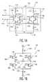
- FIGs. 1a through 1dillustrate multiple stages of a rail-to-rail common mode voltage (CMV) differential receiver circuit 100 in accordance with the preferred embodiment of the invention.
- the differential receiver circuit 100is comprised of four stages of symmetrical circuits that are disposed in series.
- FIG. 1aillustrates a differential signal splitter input stage 110, which is the first stage.
- FIG. 1billustrates the second stage, the CMV normalization stage 130.
- FIG. 1cillustrates the third stage, a transimpedance amplifier stage 150.
- FIG. 1dillustrates the fourth stage, a buffer stage, which is a rail-to-rail output driver stage 150.
- the first stage 110is comprised of two symmetrical circuit branches, a first branch 111 and a second branch 112. Disposed within the first branch 111 are a first n channel metal oxide semiconductor (NMOS) transistor (NMOS1) 113 and a first p channel metal oxide semiconductor (PMOS) transistor (PMOS1) 114. Disposed within the second branch 112 are a second NMOS transistor (NMOS2) 115 and a second PMOS transistor (PMOS2) 116.
- NMOSn channel metal oxide semiconductor
- PMOSp channel metal oxide semiconductor
- PMOS2Disposed within the second branch 112 are a second NMOS transistor (NMOS2) 115 and a second PMOS transistor (PMOS2) 116.
- resistive loadslabeled R1, 117a through 117d, electrically couple the drain and source terminals of devices NMOS1 113, PMOS1 114 and NMOS2 115, PMOS2 116 to a first and second supply voltage ports, 110c and 110d, connected for receiving of potential voltages, Vdd and Vss, respectively.
- the gate terminals of transistors PMOS1 114 and NMOS2 115are electrically coupled together and are electrically coupled with a first input port 110a, which his labeled "In+.” Gate terminals of transistors PMOS2 116 and NMOS1 113 are electrically coupled together to a second input port 110b, which is labeled "In-.”
- the first and second input ports, 110a and 110b,form the differential input ports to the first stage 110.
- the first stage 110additionally has four output ports, 110e through 110h, which are labeled: inn1, inp1, inn2, inp2, for providing of respective signals dn, sn, sp, dp, therefrom.
- the first 110 stagefunctions as a differential signal phase splitting stage.
- the input signal provided to the differential input ports, 110 and 110b, of this stageis a small differential signal with a potential of approximately 50mv to 400mv having a rail-to-rail common mode voltage (CMV).
- CMVrail-to-rail common mode voltage
- the first branch 111is comprised of the NMOS1 and PMOS1 devices, 113 and 114, which are electrically coupled together in a pass-gate configuration. Each side of this pass-gate is electrically coupled to a respective resistor, where resistors 117a and 117b respectively electrically couple the drain and source terminals of NMOS1 and PMOS1 devices, 113 and 114, to the 110c and 110d supply voltage ports. Resistors 117c and 117d are used for respective coupling of the drain and source terminals of NMOS2 and PMOS2 devices, 115 and 116, to the 110c and 110d supply voltage ports.
- FIG. 2athis figure graphically depicts what occurs when a small differential signal, "in+” and “in-,” is applied to the input ports, 110 and 110b, which are the gate terminals of the MOS devices 113 and 114.
- the input ports, 110 and 110bwhich are the gate terminals of the MOS devices 113 and 114.
- the NMOS1 device 113conduct less current.
- the total effectis to increase pass-gate impedance and therefore a decrease in the current that propagates through this first branch 111.
- FIG. 2bfor output ports 110e and 110f, an increase in the "dn" voltage and decrease in the "sn” voltage is observed as a result of the "in+” voltage rising.
- FIG. 2cillustrates four superimposed output signals, dn, sn, sp and dp, provided from respective output ports 110e through 110h for this first stage 110.
- This figurealso illustrates that starting with one differential signal, results in the generation of two complementary differential signals with a very small skew of approximately a few Pico seconds between the upper and lower sets of crossover points, labeled "A”, 201a and 201b, and "B", 202a and 202b.
- the corresponding crossover voltagemoves up or down in potential but remains relatively constant in time or in a timing relashionship.
- the differential amplitudechanges so does the differential amplitude of both complementary differential output signals.
- the pass-gate structureconducts current even when the PMOS1 device 114 is either turned off or close to being turned off. As the input CMV moves toward ground, the pass-gate structure conducts current even when the NMOS1 device 113 is either turned off or is close to being turned off.
- the differential phase splittingis performed by one of the MOS devices, which is either the NMOS1 device 113 or the PMOS1 device 114, respectively.
- the differential phase splittingworks with a rail to rail CMV.
- the differential gain of this first stageis less than unity, where it is optionally 50% of the differential input voltage.
- the dimensions of each of the PMOS and NMOS devices, 113 through 116, as well as the resistors, 117a through 117d,are chosen in order to approximately optimize for best performance of cross-over voltage and differential phase splitting.
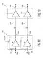
- the CMV normalization stageis shown with two NMOS devices, labeled MN1 134 and MN2 136, and two PMOS devices, labeled MP1 133 and MP2 135.
- Source terminals of devices MP1 133 and MP2 135are electrically coupled together and are further electrically coupled to a first supply voltage port 130c, for receiving of Vdd, through resistor R2 137a.
- Source terminals of devices MN1 134 and MN2 136are electrically coupled together and are further electrically coupled to a second supply voltage port 130d, for receiving of Vss, through resistor R2 137b.
- a third resistor R3 137cis disposed between a junction formed between the drain terminal of device MP1 133 and the drain terminal of device MN1 134 and a junction formed between the drain terminal of device MP2 135 and the drain terminal of device MN2 136.
- This second stageis a complementary differential stage, which is used to normalize the common mode voltage (CMV) to approximately Vdd/2.
- CMVcommon mode voltage
- a main current pathis formed from the first supply voltage port 130c, resistor R2 137a through transistor MP1 133, through resistor R3 137c, through transistor MN2 136, through resistor R2 137b and finally into the second supply voltage port 130d, which is ground, Vss.
- the PMOS and NMOS devices, 133, 135, 134, 136are designed to have equal active areas and comparable gain, gm. This equalizes capacitive loading of the first stage 110 and aids in skew and symmetry of the output signals provided from output ports, 131a and 131b of this second stage 130. With an equal gain, gm, for the transistors MP1 133, MP2 135 and MN1 134, MN2 136, positive and negative currents flowing in resistor R3 137c are equal.
- the output differential voltage provided from the output ports, 131a and 131b, of the second stage 130is centered about a CMV of Vdd/2. Furthermore, because the second stage 130 is primarily used to normalize the CMV, the voltage gain of this stage is not essential. Voltage gain is performed in the third stage 150.
- FIGs. 1c and 1dillustrate the transimpedance stages.
- Output ports of the second stage, 131a and 131bare electrically coupled with input ports 150a and 150b, with signals "in2+” and "in2-" being provided from these ports, of the third stage 150.
- the transimpedance stage 150includes two inverters, a first inverter 151 and a second inverter 152, with a respective feedback load resistor, 157a and 157b.
- Each resistor R4, 157a and 157bprovides a negative feedback to the inverter's input port, 150a or 150b, from its output port, therefore lowering a normally high gain of each inverter from few hundred, or thousands, to a small value such as five.
- the net effect of this transimpedance stage 150is that it creates an output waveform with equal rise and fall times given that the differential input signal provided to the input ports 150a and 150b is within specification.
- This third stage 150forms a resistive load to the second stage 130, since by definition, the input signal provided to the transimpedance stage input ports, 150a and 150b, is in the form of a current.
- output signals, "in3+” and “in3-”, provided from output ports, 150c and 150d, of the transimpedance stage 150are not rail to rail since a crowbar, or through current is involved. Effectively, the transimpedance stage 150 loads the second stage 130 with extra current and provides additional CMV equalization for the second stage 130. Additionally, since the output signals of the transimpedance stage 150 are controlled by design of the circuitry, signals "in3+” and "in3-,” provided from output ports 150c and 150d, are symmetrical differential signals with very low skew and are centered around Vdd/2, but are not rail-to-rail. Referring to FIG. 3c , as the first stage 110 differential input CMV change, the third stage 150 differential output signal changes in differential amplitude, but it's CMV stays constant around Vdd/2.
- the fourth stageis provided with two input ports 170a and 170b electrically coupled with the output ports 150c and 150c of the third stage 150.
- This fourth stage 170receives the output signals from the third stage 150 and buffers them using buffer circuits 171 and 172 in order to form output signals, "out+” and “out-”, on output ports 170c and 170d.
- the resulting output signals, "out+” and "out-"are rail to rail.
- this fourth stage 170is optimized to amplify and buffer the third stage 150 output signals and to preserve the low skew and rise and fall symmetry of the waveforms and the CMV.
- the differential receiver in accordance with the embodiment of the inventionis useable with high speed, or optionally low speed, differential signal amplification and signal communication where low skew and high symmetry are preferred.
Landscapes
- Engineering & Computer Science (AREA)
- Power Engineering (AREA)
- Amplifiers (AREA)
Abstract
Description
- The invention relates to the field of differential receiver circuits and more specifically to the field of differential receiver circuits with rail-to-rail common mode operation with differential output signal low skew and symmetry.
- One conventional technique used for receiving of low swing differential signals, having a rail to rail common mode voltage (CMV) range, is to utilize two receiver circuits. The first receiver circuit is, for example, a NMOS type input transistor, which is used to receive a signal with a CMV close to a supply voltage potential (Vdd) and a PMOS type input transistor for receiving a signal with a CMV close to ground potential, gnd. Output signals from the two receiver circuits are then combined into a single ended output signal from an output port thereof. The differential receiver circuits are typically of any form of differential amplifier, however, the most common differential amplifiers are typically highly accurate folded cascode ones.
- United States Patent Number
5,801,564 discloses a reduced skew differential receiver that utilizes first and second differential amplifiers. Unfortunately, careful coupling of the two differential amplifiers is required in order to attain predetermined operation. Additionally, this circuit is quite complex and as a result affects the creation of low skew and symmetry in the differential output signal. - United States Patent
US6,535,062 discloses a low noise, low distortion, complimentary IF amplifier. European Patent application publicationEP1,248,371 discloses a convertor for converting the level of differential signals. - A need therefore exists to provide a high-speed performance differential receiver with low skew and a symmetrical differential output signal at a low design cost. It is therefore an object of the invention to provide a differential receiver circuit with rail-to-rail common mode operation while providing differential output signal low skew and symmetry.
- In accordance with the invention there is provided a differential receiver circuit as defined in
claim 1. - Exemplary embodiments of the invention will now be described in conjunction with the following drawings, in which:
FIG. 1a illustrates a differential signal splitter input stage, which is the first stage of a rail-to-rail common mode voltage (CMV) differential receiver circuit;FIG. 1b illustrates a CMV normalization stage, which is a second stage of the rail-to-rail CMV differential receiver circuit;FIG. 1c a transimpedance amplifier stage, which is a third stage of the rail-to-rail CMV differential receiver circuit;FIG. 1d illustrates a buffer stage, which is a rail-to-rail output driver stage, which is a fourth stage of the rail-to-rail CMV differential receiver circuit;FIG. 2a graphically depicts small differential signal input signal, "in+" and "in-", which is provided to differential input ports of the rail-to-rail CMV differential receiver circuit;FIG. 2b illustrates an increase in the "dn" voltage and decrease the "sn" voltage as a result of the "in+" voltage rising;FIG. 2c illustrates a decrease in the "sp" voltage and an increase in the "dp" voltage as a result of the "in+" voltage rising;FIG. 3a illustrates output signals, "in2-" and "in2+", provided from output ports of the second stage;FIG. 3b illustrates output signals, "in3-" and "in3+", provided from output ports of the third stage; and,FIG. 3c illustrates output signals, "out-" and "out+", provided from output ports of the rail-to-rail CMV differential receiver circuit.FIGs. 1a through 1d illustrate multiple stages of a rail-to-rail common mode voltage (CMV)differential receiver circuit 100 in accordance with the preferred embodiment of the invention. Thedifferential receiver circuit 100 is comprised of four stages of symmetrical circuits that are disposed in series.FIG. 1a illustrates a differential signalsplitter input stage 110, which is the first stage.FIG. 1b illustrates the second stage, theCMV normalization stage 130.FIG. 1c illustrates the third stage, atransimpedance amplifier stage 150.FIG. 1d illustrates the fourth stage, a buffer stage, which is a rail-to-railoutput driver stage 150.- Referring to
FIG. 1a , thefirst stage 110 is comprised of two symmetrical circuit branches, afirst branch 111 and asecond branch 112. Disposed within thefirst branch 111 are a first n channel metal oxide semiconductor (NMOS) transistor (NMOS1) 113 and a first p channel metal oxide semiconductor (PMOS) transistor (PMOS1) 114. Disposed within thesecond branch 112 are a second NMOS transistor (NMOS2) 115 and a second PMOS transistor (PMOS2) 116. Four resistive loads, labeled R1, 117a through 117d, electrically couple the drain and source terminals ofdevices NMOS1 113,PMOS1 114 andNMOS2 115,PMOS2 116 to a first and second supply voltage ports, 110c and 110d, connected for receiving of potential voltages, Vdd and Vss, respectively. - The gate terminals of
transistors PMOS1 114 andNMOS2 115 are electrically coupled together and are electrically coupled with afirst input port 110a, which his labeled "In+." Gate terminals oftransistors PMOS2 116 andNMOS1 113 are electrically coupled together to asecond input port 110b, which is labeled "In-." The first and second input ports, 110a and 110b, form the differential input ports to thefirst stage 110. Thefirst stage 110 additionally has four output ports, 110e through 110h, which are labeled: inn1, inp1, inn2, inp2, for providing of respective signals dn, sn, sp, dp, therefrom. - In use, the first 110 stage functions as a differential signal phase splitting stage. The input signal provided to the differential input ports, 110 and 110b, of this stage is a small differential signal with a potential of approximately 50mv to 400mv having a rail-to-rail common mode voltage (CMV).
- The
first branch 111 is comprised of the NMOS1 and PMOS1 devices, 113 and 114, which are electrically coupled together in a pass-gate configuration. Each side of this pass-gate is electrically coupled to a respective resistor, whereresistors Resistors - Referring to
FIG. 2a , this figure graphically depicts what occurs when a small differential signal, "in+" and "in-," is applied to the input ports, 110 and 110b, which are the gate terminals of theMOS devices PMOS1 device 114 conduct less current and the same, but opposite, occurs for theNMOS1 device 113. For theinput port 110b, as the potential of the signal "In-" falls theNMOS1 device 113 conduct less current. The total effect is to increase pass-gate impedance and therefore a decrease in the current that propagates through thisfirst branch 111. As is shown inFIG. 2b , foroutput ports 110e and 110f, an increase in the "dn" voltage and decrease in the "sn" voltage is observed as a result of the "in+" voltage rising. - A similar type of event is observed in the
second branch 112, but with opposite effects to that of thefirst branch 111. Referring toFIG. 2c , this transition of the "in+" voltage rising results in a decrease in the "sp" voltage and an increase in the "dp" voltage, as observed on the 110g and 110h output ports.FIG. 2d illustrates four superimposed output signals, dn, sn, sp and dp, provided from respective output ports 110e through 110h for thisfirst stage 110. This figure also illustrates that starting with one differential signal, results in the generation of two complementary differential signals with a very small skew of approximately a few Pico seconds between the upper and lower sets of crossover points, labeled "A", 201a and 201b, and "B", 202a and 202b. Furthermore, as the input CMV change, the corresponding crossover voltage moves up or down in potential but remains relatively constant in time or in a timing relashionship. Also, as the differential amplitude changes so does the differential amplitude of both complementary differential output signals. - Referring back to
FIG. 1a , as the input CMV moves toward higher Vdd potentials, the pass-gate structure conducts current even when thePMOS1 device 114 is either turned off or close to being turned off. As the input CMV moves toward ground, the pass-gate structure conducts current even when theNMOS1 device 113 is either turned off or is close to being turned off. - So in extreme cases for the CMV, either towards higher Vdd or lower Vss, the differential phase splitting is performed by one of the MOS devices, which is either the
NMOS1 device 113 or thePMOS1 device 114, respectively. In the case of extreme CMV, when thefirst branch 111 is conducting more current than thesecond branch 112, the differential phase splitting works with a rail to rail CMV. - Optionally, the differential gain of this first stage is less than unity, where it is optionally 50% of the differential input voltage. Preferably, during integrated manufacturing, the dimensions of each of the PMOS and NMOS devices, 113 through 116, as well as the resistors, 117a through 117d, are chosen in order to approximately optimize for best performance of cross-over voltage and differential phase splitting.
- Referring back to
FIG. 1b , the CMV normalization stage is shown with two NMOS devices, labeledMN1 134 andMN2 136, and two PMOS devices, labeledMP1 133 andMP2 135. Source terminals ofdevices MP1 133 andMP2 135 are electrically coupled together and are further electrically coupled to a firstsupply voltage port 130c, for receiving of Vdd, throughresistor R2 137a. Source terminals ofdevices MN1 134 andMN2 136 are electrically coupled together and are further electrically coupled to a secondsupply voltage port 130d, for receiving of Vss, throughresistor R2 137b. Athird resistor R3 137c is disposed between a junction formed between the drain terminal ofdevice MP1 133 and the drain terminal ofdevice MN1 134 and a junction formed between the drain terminal ofdevice MP2 135 and the drain terminal ofdevice MN2 136. - Gate terminals of the PMOS devices,
MP1 133 andMP2 135,form input ports second stage 130 and are electrically coupled withoutput ports MN1 134 andMN2 136, are electrically coupled to the output ports, 110e and 110g, of the first stage top side. This second stage is a complementary differential stage, which is used to normalize the common mode voltage (CMV) to approximately Vdd/2. - Referring to FIG. 3a, when the input voltage "inp1," provided to input
port 130e, is lower than the input voltage "inp2," provided to inputport 130g, and when the input voltage "inn2," provided to inputport 130f, is higher than "inn1," provided to inputport 130h, a positive current path flows throughresistor R3 137c fromnode 131 a, as is indicated by signal "in2-", towardnode 131b, as is indicated by signal "in2+". A main current path is formed from the firstsupply voltage port 130c,resistor R2 137a throughtransistor MP1 133, throughresistor R3 137c, throughtransistor MN2 136, throughresistor R2 137b and finally into the secondsupply voltage port 130d, which is ground, Vss. - When the input conditions are reversed, the reverse is true. A positive current propagates through resistor R3 from
node 131b, "in2+", tonode 131a, "in2-". Preferably, the PMOS and NMOS devices, 133, 135, 134, 136 are designed to have equal active areas and comparable gain, gm. This equalizes capacitive loading of thefirst stage 110 and aids in skew and symmetry of the output signals provided from output ports, 131a and 131b of thissecond stage 130. With an equal gain, gm, for thetransistors MP1 133,MP2 135 andMN1 134,MN2 136, positive and negative currents flowing inresistor R3 137c are equal. Therefore, the output differential voltage provided from the output ports, 131a and 131b, of thesecond stage 130 is centered about a CMV of Vdd/2. Furthermore, because thesecond stage 130 is primarily used to normalize the CMV, the voltage gain of this stage is not essential. Voltage gain is performed in thethird stage 150. - Furthermore, for
FIG. 3a , as the differential input CMV changes for thefirst stage 110, the four output signals provided from the output ports, 110e through 110h, shift up and down in potential. Referring toFIG. 3b , as thesecond stage 130 differential output signal, provided fromoutput ports - Referring back to
FIGs. 1c and 1d , these figures illustrate the transimpedance stages. Output ports of the second stage, 131a and 131b, are electrically coupled withinput ports third stage 150. Thetransimpedance stage 150 includes two inverters, afirst inverter 151 and asecond inverter 152, with a respective feedback load resistor, 157a and 157b. Each resistor R4, 157a and 157b, provides a negative feedback to the inverter's input port, 150a or 150b, from its output port, therefore lowering a normally high gain of each inverter from few hundred, or thousands, to a small value such as five. The net effect of thistransimpedance stage 150 is that it creates an output waveform with equal rise and fall times given that the differential input signal provided to theinput ports third stage 150 forms a resistive load to thesecond stage 130, since by definition, the input signal provided to the transimpedance stage input ports, 150a and 150b, is in the form of a current. - Referring to
FIG. 3b , output signals, "in3+" and "in3-", provided from output ports, 150c and 150d, of thetransimpedance stage 150 are not rail to rail since a crowbar, or through current is involved. Effectively, thetransimpedance stage 150 loads thesecond stage 130 with extra current and provides additional CMV equalization for thesecond stage 130. Additionally, since the output signals of thetransimpedance stage 150 are controlled by design of the circuitry, signals "in3+" and "in3-," provided fromoutput ports FIG. 3c , as thefirst stage 110 differential input CMV change, thethird stage 150 differential output signal changes in differential amplitude, but it's CMV stays constant around Vdd/2. - Referring to
FIG. 1d , the fourth stage is provided with twoinput ports output ports third stage 150. Thisfourth stage 170 receives the output signals from thethird stage 150 and buffers them usingbuffer circuits 171 and 172 in order to form output signals, "out+" and "out-", onoutput ports fourth stage 170 is optimized to amplify and buffer thethird stage 150 output signals and to preserve the low skew and rise and fall symmetry of the waveforms and the CMV. - Advantageously, the differential receiver in accordance with the embodiment of the invention is useable with high speed, or optionally low speed, differential signal amplification and signal communication where low skew and high symmetry are preferred.
- Numerous other embodiments may be envisaged without departing from the scope of the invention.
Claims (16)
- A differential receiver circuit comprising:a first supply voltage port (110c; 130c) as a first rail for receiving of a first potential; anda second supply voltage port (110d; 130d) as a second rail for receiving of a second potential that is lower than the first potential,a differential signal splitter (110) comprising a first branch (111) and a second branch (112) disposed between the first supply voltage port (110c) and the second supply voltage port (110) and a first input port (110a) and a second input port (110b) for receiving of a differential input signal and first through fourth output ports (110e, 110f, 110g, 110h) for providing of two complementary differential output signals therefrom;a common mode voltage, CMV, normalization stage (130) for level shifting the two complementary differential output signals to form one complementary differential output signal, the CMV normalization stage (130) comprising first through fourth input ports (130e, 130f, 130g, 130h) electrically coupled with the first through fourth output ports (110e, 110f, 110g, 110h) of the differential signal splitter stage (110) and first and second output ports (131a, 131b);a transimpedance amplifier (150) comprising first and second input ports (150a, 150b) electrically coupled with the first and second output ports (131a, 131b) of the CMV normalization stage (130) and first and second output ports (150c, 150d) for providing a rail to rail complementary differential output signal having low signal skew and symmetry,wherein the differential signal splitter (110), the common mode voltage, CMV, normalization stage (130) and the transimpedance amplifier (150) are disposed between the first supply voltage port (110c; 130c) and the second supply voltage port (110d; 130d) for receiving of the first and second potentials therefrom,wherein the first branch (111) comprises:a first PMOS device (114) having gate, drain and source terminals;a first NMOS device (113) having a gate terminal and drain and source terminals electrically coupled with the drain and source terminals of the first PMOS device (114), wherein the second branch (112) comprises:a second PMOS device (116) having gate, drain and source terminals;a second NMOS device (115) having a gate terminal and drain and source terminals electrically coupled with the drain and source terminals of the second PMOS device (116),where the gate terminals of the first PMOS device (114) and the second NMOS device (115) are electrically coupled together and form the first input port (110a) of the differential signal splitter stage (110) and the gate terminals of the second PMOS device (116) and the first NMOS device (113) form the second input port (110b) of the differential signal splitter stage (110).
- A differential receiver circuit according to claim 1 comprising a buffer stage (170) comprising a first input port (170a) and a second input port (170b) electrically coupled with the first output port (150c) and the second output port (150d) of the transimpedance amplifier (150) and a first output port (170c) and a second output port (170d) for providing the rail to rail complimentary differential output signal.
- A differential receiver circuit according to claim 1 wherein the NMOS (113, 115) devices and PMOS devices (114, 116) comprise approximately equal active areas and approximately equal gains.
- A differential receiver circuit according to claim 1:wherein the first branch (111) comprises a first set of two approximately identical resistors (117a, 117b) respectively disposed between the drain terminals of the electrically coupled first NMOS (113) device and first PMOS device (114) and the first supply voltage port (110c) and between the source terminals of the electrically coupled first NMOS device (113) and first PMOS device (114) and the second supply voltage port (110d),wherein the first output port (110e) and the second output port (110f) of the differential signal splitter stage (110) are formed respectively at the electrically coupled drain and source terminals of the first NMOS device (113) and the first PMOS device (114).
- A differential receiver circuit according to claim 4 wherein the second branch (112) comprises a second set of two approximately identical resistors (117c, 117d), which are approximately identical to the first set of resistors (117a, 117b), respectively disposed between the drain terminals of the electrically coupled second NMOS device (115) and second PMOS device (116) and the first supply voltage port (110c) and between the source terminals of the electrically coupled second NMOS device (115) and second PMOS device (116) and the second supply voltage port (110d), wherein the third output port (110g) and the fourth output port (110h) of the differential signal splitter stage (110) are formed respectively at the electrically coupled drain and source terminals of the second NMOS device (115) and second PMOS device (116).
- A differential receiver circuit according to claim 1 wherein the common mode voltage, CMV, normalization stage (130) comprises:a first branch;a second branch; and,a first resistive coupling (137a) between a first end of both branches to the first supply voltage port (130c) and a second resistive coupling (137b) between a second end of both branches to the second supply voltage port (130d), wherein resistance values for the first resistive coupling (137a) and second resistive coupling (137b) are approximately equal.
- A differential receiver circuit according to claim 6 wherein the first branch of the CMV normalization stage (130) comprises:a first PMOS device (133) having a gate terminal electrically coupled with the first input port (130e) of the CMV normalization stage (130), a source terminal electrically coupled to the first end of the first branch and a drain terminal; and,a first NMOS device (134) having a gate terminal electrically coupled with the second input port (130f) of the CMV normalization stage (130), a drain terminal electrically coupled to the drain terminal of the first PMOS device (133), for forming the first output port (131a) of the CMV normalization stage (130), and the source terminal thereof electrically coupled to the second end of the first branch.
- A differential receiver circuit according to claim 7 wherein the second branch of the CMV normalization stage (130) comprises:a second PMOS device (135) having a gate terminal electrically coupled with the third input port (130g) of the CMV normalization stage (130), a source terminal electrically coupled to the first end of the second branch and a drain terminal; and,a second NMOS device (136) having a gate terminal electrically coupled with the fourth input port (130h) of the CMV normalization stage (130), a drain terminal electrically coupled to the drain terminal of the second PMOS device (135), for forming the second output port (131b) of the CMV normalization stage (130), and the source terminal thereof electrically coupled to the second end of the second branch.
- A differential receiver circuit according to claim 8 wherein the NMOS devices (134, 136) and PMOS devices (133, 135) comprise approximately equal active areas and approximately equal gains.
- A differential receiver circuit according to claim 1 comprising a third resistor (137c) disposed between the first output port (131a) and the second output port (131b) of the CMV normalization stage (130).
- A differential receiver circuit according to claim 1 wherein the transimpedance amplifier (150) comprises:a first inverter circuit (151) disposed between the first input port (150a) and the first output port (150c) of the transimpedance amplification stage (150); and,a fourth resistor (157a) disposed in parallel with the first inverter circuit (151).
- A differential receiver circuit according to claim 11 wherein the transimpedance amplifier comprises:a second inverter circuit (152) disposed between the second input port (150b) and the second output port (150d) of the transimpedance amplification stage (150); and,a fourth resistor (157b) disposed in parallel with the second inverter circuit (152).
- A differential receiver circuit according to claim 2 wherein the buffer stage (170) comprises a first buffer circuit (171) disposed between the first input port (170a) and the first output port (170c) of the buffer stage (170).
- A differential receiver circuit according to claim 13 wherein the buffer stage (170) comprises a second buffer circuit (172) disposed between the second input port (170b) and the second output port (170d) of the buffer stage (170).
- A differential receiver circuit according to claim 1 wherein the differential input signal has a potential of approximately 50mv to 400mv and has a rail-to-rail common mode voltage, CMV.
- A differential receiver circuit according to claim 2 comprising a same integrated circuit semiconductor substrate, wherein the differential signal splitter (110), the CMV normalization stage (130), the transimpedance amplifier circuit (150) and the buffer stage (170) are integrated within the same integrated circuit semiconductor substrate.
Applications Claiming Priority (2)
| Application Number | Priority Date | Filing Date | Title |
|---|---|---|---|
| US56345504P | 2004-04-20 | 2004-04-20 | |
| PCT/IB2005/051278WO2005104356A1 (en) | 2004-04-20 | 2005-04-19 | High speed differential receiver with rail to rail common mode operation having a symmetrical differential output signal with low skew |
Publications (2)
| Publication Number | Publication Date |
|---|---|
| EP1741180A1 EP1741180A1 (en) | 2007-01-10 |
| EP1741180B1true EP1741180B1 (en) | 2012-01-11 |
Family
ID=34966282
Family Applications (1)
| Application Number | Title | Priority Date | Filing Date |
|---|---|---|---|
| EP05733767AExpired - LifetimeEP1741180B1 (en) | 2004-04-20 | 2005-04-19 | High speed differential receiver with rail to rail common mode operation having a symmetrical differential output signal with low skew |
Country Status (6)
| Country | Link |
|---|---|
| US (1) | US7724087B2 (en) |
| EP (1) | EP1741180B1 (en) |
| JP (1) | JP2007534258A (en) |
| CN (1) | CN100576725C (en) |
| AT (1) | ATE541358T1 (en) |
| WO (1) | WO2005104356A1 (en) |
Families Citing this family (31)
| Publication number | Priority date | Publication date | Assignee | Title |
|---|---|---|---|---|
| CN101185239B (en)* | 2005-05-26 | 2011-03-30 | 哉英电子股份有限公司 | signal conversion circuit |
| US9563733B2 (en) | 2009-05-06 | 2017-02-07 | Tela Innovations, Inc. | Cell circuit and layout with linear finfet structures |
| US7956421B2 (en) | 2008-03-13 | 2011-06-07 | Tela Innovations, Inc. | Cross-coupled transistor layouts in restricted gate level layout architecture |
| US8658542B2 (en) | 2006-03-09 | 2014-02-25 | Tela Innovations, Inc. | Coarse grid design methods and structures |
| US7763534B2 (en) | 2007-10-26 | 2010-07-27 | Tela Innovations, Inc. | Methods, structures and designs for self-aligning local interconnects used in integrated circuits |
| US8541879B2 (en) | 2007-12-13 | 2013-09-24 | Tela Innovations, Inc. | Super-self-aligned contacts and method for making the same |
| US8653857B2 (en) | 2006-03-09 | 2014-02-18 | Tela Innovations, Inc. | Circuitry and layouts for XOR and XNOR logic |
| US8839175B2 (en) | 2006-03-09 | 2014-09-16 | Tela Innovations, Inc. | Scalable meta-data objects |
| US8448102B2 (en) | 2006-03-09 | 2013-05-21 | Tela Innovations, Inc. | Optimizing layout of irregular structures in regular layout context |
| US9009641B2 (en) | 2006-03-09 | 2015-04-14 | Tela Innovations, Inc. | Circuits with linear finfet structures |
| US9035359B2 (en) | 2006-03-09 | 2015-05-19 | Tela Innovations, Inc. | Semiconductor chip including region including linear-shaped conductive structures forming gate electrodes and having electrical connection areas arranged relative to inner region between transistors of different types and associated methods |
| US7446352B2 (en) | 2006-03-09 | 2008-11-04 | Tela Innovations, Inc. | Dynamic array architecture |
| US9230910B2 (en) | 2006-03-09 | 2016-01-05 | Tela Innovations, Inc. | Oversized contacts and vias in layout defined by linearly constrained topology |
| US8667443B2 (en) | 2007-03-05 | 2014-03-04 | Tela Innovations, Inc. | Integrated circuit cell library for multiple patterning |
| US7888705B2 (en) | 2007-08-02 | 2011-02-15 | Tela Innovations, Inc. | Methods for defining dynamic array section with manufacturing assurance halo and apparatus implementing the same |
| JP5022789B2 (en)* | 2007-06-27 | 2012-09-12 | ザインエレクトロニクス株式会社 | Signal conversion circuit and rail-to-rail circuit |
| US7595691B2 (en)* | 2007-09-04 | 2009-09-29 | Himax Technologies Limited | Pre-amplifier for a receiver and a method therefor |
| WO2009063373A2 (en) | 2007-11-12 | 2009-05-22 | Nxp B.V. | Signal processor comprising an amplifier |
| US8453094B2 (en) | 2008-01-31 | 2013-05-28 | Tela Innovations, Inc. | Enforcement of semiconductor structure regularity for localized transistors and interconnect |
| US7939443B2 (en) | 2008-03-27 | 2011-05-10 | Tela Innovations, Inc. | Methods for multi-wire routing and apparatus implementing same |
| SG192532A1 (en) | 2008-07-16 | 2013-08-30 | Tela Innovations Inc | Methods for cell phasing and placement in dynamic array architecture and implementation of the same |
| US9122832B2 (en) | 2008-08-01 | 2015-09-01 | Tela Innovations, Inc. | Methods for controlling microloading variation in semiconductor wafer layout and fabrication |
| CN101651646B (en)* | 2009-09-02 | 2013-07-03 | 中兴通讯股份有限公司 | Differential receiving system of cellular receiver and method for realizing signal reception |
| US8661392B2 (en) | 2009-10-13 | 2014-02-25 | Tela Innovations, Inc. | Methods for cell boundary encroachment and layouts implementing the Same |
| US9159627B2 (en) | 2010-11-12 | 2015-10-13 | Tela Innovations, Inc. | Methods for linewidth modification and apparatus implementing the same |
| US8305113B1 (en)* | 2011-05-04 | 2012-11-06 | Texas Instruments Incorporated | Intra-pair skew cancellation technique for differential signaling |
| CN103825598B (en)* | 2012-11-19 | 2018-11-13 | 恩智浦美国有限公司 | Differential buffers input stage between rail |
| CN105099436B (en)* | 2014-05-13 | 2019-03-26 | 华邦电子股份有限公司 | Rail-to-rail input buffer |
| US9419644B2 (en)* | 2014-08-19 | 2016-08-16 | Intersil Americas LLC | System, circuit and method for converting a differential voltage signal including a high common mode voltage component to a ground referenced signal for battery voltage managment |
| CN109905111B (en)* | 2019-03-06 | 2020-06-30 | 电子科技大学 | Level shift circuit suitable for GaN high-speed gate drive circuit |
| US10581645B1 (en)* | 2019-05-30 | 2020-03-03 | Nvidia Corp. | Dual-rail transceiver with improved signal-to-noise ratio for differential high-speed links |
Family Cites Families (12)
| Publication number | Priority date | Publication date | Assignee | Title |
|---|---|---|---|---|
| US4818929A (en) | 1988-07-01 | 1989-04-04 | American Telephone And Telegraph Company, At&T Bell Laboratories | Fully differential analog comparator |
| US5734294A (en)* | 1996-02-15 | 1998-03-31 | Raytheon Company | Large swing wide band high order programmable active filters |
| US5801564A (en) | 1996-06-28 | 1998-09-01 | Symbios, Inc. | Reduced skew differential receiver |
| US5936469A (en)* | 1997-08-04 | 1999-08-10 | Motorola, Inc. | Amplifier with input referred common-mode adjustment |
| US5986511A (en)* | 1997-10-31 | 1999-11-16 | International Business Machines Corporation | Frequency dependent impedance |
| US6204980B1 (en)* | 1998-06-18 | 2001-03-20 | Adaptec, Inc. | High speed gain stage with DC offset cancellation for servo demodulator circuit |
| US6084478A (en)* | 1998-08-20 | 2000-07-04 | Vitesse Semiconductor Corp. | Transimpedance amplifier with automatic gain control |
| US6535062B1 (en) | 2000-06-30 | 2003-03-18 | Raytheon Company | Low noise, low distortion, complementary IF amplifier |
| EP1248371A1 (en) | 2001-04-06 | 2002-10-09 | STMicroelectronics S.r.l. | A converter for converting the level of differential signals |
| US6686772B2 (en)* | 2001-11-19 | 2004-02-03 | Broadcom Corporation | Voltage mode differential driver and method |
| US6784750B2 (en)* | 2002-04-09 | 2004-08-31 | Microsemi Corporation | Transimpedance amplifier with selective DC compensation |
| US7400173B1 (en)* | 2003-09-19 | 2008-07-15 | Cypress Semicondductor Corp. | Differential receiver with wide input common mode range and low duty cycle distortion |
- 2005
- 2005-04-19EPEP05733767Apatent/EP1741180B1/ennot_activeExpired - Lifetime
- 2005-04-19USUS11/587,103patent/US7724087B2/ennot_activeExpired - Lifetime
- 2005-04-19ATAT05733767Tpatent/ATE541358T1/enactive
- 2005-04-19CNCN200580011854Apatent/CN100576725C/ennot_activeExpired - Fee Related
- 2005-04-19WOPCT/IB2005/051278patent/WO2005104356A1/enactiveApplication Filing
- 2005-04-19JPJP2007509040Apatent/JP2007534258A/ennot_activeWithdrawn
Also Published As
| Publication number | Publication date |
|---|---|
| JP2007534258A (en) | 2007-11-22 |
| US7724087B2 (en) | 2010-05-25 |
| WO2005104356A1 (en) | 2005-11-03 |
| ATE541358T1 (en) | 2012-01-15 |
| US20080258812A1 (en) | 2008-10-23 |
| EP1741180A1 (en) | 2007-01-10 |
| CN100576725C (en) | 2009-12-30 |
| CN1943107A (en) | 2007-04-04 |
Similar Documents
| Publication | Publication Date | Title |
|---|---|---|
| EP1741180B1 (en) | High speed differential receiver with rail to rail common mode operation having a symmetrical differential output signal with low skew | |
| EP2498398B1 (en) | Amplifier circuit and method | |
| US6429747B2 (en) | System and method for converting from single-ended to differential signals | |
| US10637695B1 (en) | High-speed low-voltage serial link receiver and method thereof | |
| CN101521489A (en) | Amplifier and class AB amplifier | |
| US6236269B1 (en) | Complementary CMOS differential amplifier circuit | |
| US20060012429A1 (en) | Self biased differential amplifier | |
| US7929241B1 (en) | Signal conversion system and method | |
| CN100568712C (en) | High speed rail-to-rail phase splitter providing symmetric differential output signals with low skew | |
| JP4371618B2 (en) | Differential amplifier circuit | |
| US20070046333A1 (en) | Differential output circuit with stable duty | |
| CN101453195A (en) | Method for improving common mode feedback stability by using grounding capacitor | |
| US6710660B1 (en) | Class B power buffer with rail to rail output swing and small deadband | |
| US8816770B2 (en) | Low-voltage constant-gm rail-to-rail CMOS input stage with improved gain | |
| CN117546409A (en) | Split miller compensation in a two-stage differential amplifier | |
| US7315210B2 (en) | Differential operational amplifier | |
| US7663443B2 (en) | Active balun circuit | |
| US12074739B1 (en) | Continuous time linear equalizer of single-ended signal with input coupling capacitor | |
| US20090160559A1 (en) | Integrated circuit including impedance to provide symmetrical differential signals | |
| US7113040B2 (en) | Differential amplifier | |
| JP4180307B2 (en) | Low input impedance amplifier | |
| TW202527480A (en) | Cascode amplifier with dynamic body bias and method thereof | |
| US8963582B2 (en) | Signal amplification circuit and method | |
| US20120007674A1 (en) | Power amplifier reducing gain mismatch | |
| JP2008124735A (en) | Differential comparator |
Legal Events
| Date | Code | Title | Description |
|---|---|---|---|
| PUAI | Public reference made under article 153(3) epc to a published international application that has entered the european phase | Free format text:ORIGINAL CODE: 0009012 | |
| 17P | Request for examination filed | Effective date:20061120 | |
| AK | Designated contracting states | Kind code of ref document:A1 Designated state(s):AT BE BG CH CY CZ DE DK EE ES FI FR GB GR HU IE IS IT LI LT LU MC NL PL PT RO SE SI SK TR | |
| DAX | Request for extension of the european patent (deleted) | ||
| RAP1 | Party data changed (applicant data changed or rights of an application transferred) | Owner name:NXP B.V. | |
| 17Q | First examination report despatched | Effective date:20100930 | |
| GRAP | Despatch of communication of intention to grant a patent | Free format text:ORIGINAL CODE: EPIDOSNIGR1 | |
| GRAS | Grant fee paid | Free format text:ORIGINAL CODE: EPIDOSNIGR3 | |
| GRAA | (expected) grant | Free format text:ORIGINAL CODE: 0009210 | |
| AK | Designated contracting states | Kind code of ref document:B1 Designated state(s):AT BE BG CH CY CZ DE DK EE ES FI FR GB GR HU IE IS IT LI LT LU MC NL PL PT RO SE SI SK TR | |
| REG | Reference to a national code | Ref country code:GB Ref legal event code:FG4D | |
| REG | Reference to a national code | Ref country code:CH Ref legal event code:EP | |
| REG | Reference to a national code | Ref country code:AT Ref legal event code:REF Ref document number:541358 Country of ref document:AT Kind code of ref document:T Effective date:20120115 | |
| REG | Reference to a national code | Ref country code:IE Ref legal event code:FG4D | |
| REG | Reference to a national code | Ref country code:DE Ref legal event code:R096 Ref document number:602005032109 Country of ref document:DE Effective date:20120308 | |
| REG | Reference to a national code | Ref country code:NL Ref legal event code:VDEP Effective date:20120111 | |
| PG25 | Lapsed in a contracting state [announced via postgrant information from national office to epo] | Ref country code:SI Free format text:LAPSE BECAUSE OF FAILURE TO SUBMIT A TRANSLATION OF THE DESCRIPTION OR TO PAY THE FEE WITHIN THE PRESCRIBED TIME-LIMIT Effective date:20120111 | |
| LTIE | Lt: invalidation of european patent or patent extension | Effective date:20120111 | |
| PG25 | Lapsed in a contracting state [announced via postgrant information from national office to epo] | Ref country code:LT Free format text:LAPSE BECAUSE OF FAILURE TO SUBMIT A TRANSLATION OF THE DESCRIPTION OR TO PAY THE FEE WITHIN THE PRESCRIBED TIME-LIMIT Effective date:20120111 Ref country code:IS Free format text:LAPSE BECAUSE OF FAILURE TO SUBMIT A TRANSLATION OF THE DESCRIPTION OR TO PAY THE FEE WITHIN THE PRESCRIBED TIME-LIMIT Effective date:20120511 Ref country code:BG Free format text:LAPSE BECAUSE OF FAILURE TO SUBMIT A TRANSLATION OF THE DESCRIPTION OR TO PAY THE FEE WITHIN THE PRESCRIBED TIME-LIMIT Effective date:20120411 Ref country code:BE Free format text:LAPSE BECAUSE OF FAILURE TO SUBMIT A TRANSLATION OF THE DESCRIPTION OR TO PAY THE FEE WITHIN THE PRESCRIBED TIME-LIMIT Effective date:20120111 Ref country code:NL Free format text:LAPSE BECAUSE OF FAILURE TO SUBMIT A TRANSLATION OF THE DESCRIPTION OR TO PAY THE FEE WITHIN THE PRESCRIBED TIME-LIMIT Effective date:20120111 | |
| PG25 | Lapsed in a contracting state [announced via postgrant information from national office to epo] | Ref country code:GR Free format text:LAPSE BECAUSE OF FAILURE TO SUBMIT A TRANSLATION OF THE DESCRIPTION OR TO PAY THE FEE WITHIN THE PRESCRIBED TIME-LIMIT Effective date:20120412 Ref country code:PL Free format text:LAPSE BECAUSE OF FAILURE TO SUBMIT A TRANSLATION OF THE DESCRIPTION OR TO PAY THE FEE WITHIN THE PRESCRIBED TIME-LIMIT Effective date:20120111 Ref country code:FI Free format text:LAPSE BECAUSE OF FAILURE TO SUBMIT A TRANSLATION OF THE DESCRIPTION OR TO PAY THE FEE WITHIN THE PRESCRIBED TIME-LIMIT Effective date:20120111 Ref country code:PT Free format text:LAPSE BECAUSE OF FAILURE TO SUBMIT A TRANSLATION OF THE DESCRIPTION OR TO PAY THE FEE WITHIN THE PRESCRIBED TIME-LIMIT Effective date:20120511 | |
| REG | Reference to a national code | Ref country code:AT Ref legal event code:MK05 Ref document number:541358 Country of ref document:AT Kind code of ref document:T Effective date:20120111 | |
| PG25 | Lapsed in a contracting state [announced via postgrant information from national office to epo] | Ref country code:CY Free format text:LAPSE BECAUSE OF FAILURE TO SUBMIT A TRANSLATION OF THE DESCRIPTION OR TO PAY THE FEE WITHIN THE PRESCRIBED TIME-LIMIT Effective date:20120111 | |
| PG25 | Lapsed in a contracting state [announced via postgrant information from national office to epo] | Ref country code:RO Free format text:LAPSE BECAUSE OF FAILURE TO SUBMIT A TRANSLATION OF THE DESCRIPTION OR TO PAY THE FEE WITHIN THE PRESCRIBED TIME-LIMIT Effective date:20120111 Ref country code:EE Free format text:LAPSE BECAUSE OF FAILURE TO SUBMIT A TRANSLATION OF THE DESCRIPTION OR TO PAY THE FEE WITHIN THE PRESCRIBED TIME-LIMIT Effective date:20120111 Ref country code:CZ Free format text:LAPSE BECAUSE OF FAILURE TO SUBMIT A TRANSLATION OF THE DESCRIPTION OR TO PAY THE FEE WITHIN THE PRESCRIBED TIME-LIMIT Effective date:20120111 Ref country code:DK Free format text:LAPSE BECAUSE OF FAILURE TO SUBMIT A TRANSLATION OF THE DESCRIPTION OR TO PAY THE FEE WITHIN THE PRESCRIBED TIME-LIMIT Effective date:20120111 Ref country code:SE Free format text:LAPSE BECAUSE OF FAILURE TO SUBMIT A TRANSLATION OF THE DESCRIPTION OR TO PAY THE FEE WITHIN THE PRESCRIBED TIME-LIMIT Effective date:20120111 | |
| PLBE | No opposition filed within time limit | Free format text:ORIGINAL CODE: 0009261 | |
| STAA | Information on the status of an ep patent application or granted ep patent | Free format text:STATUS: NO OPPOSITION FILED WITHIN TIME LIMIT | |
| PG25 | Lapsed in a contracting state [announced via postgrant information from national office to epo] | Ref country code:IT Free format text:LAPSE BECAUSE OF FAILURE TO SUBMIT A TRANSLATION OF THE DESCRIPTION OR TO PAY THE FEE WITHIN THE PRESCRIBED TIME-LIMIT Effective date:20120111 Ref country code:MC Free format text:LAPSE BECAUSE OF NON-PAYMENT OF DUE FEES Effective date:20120430 Ref country code:SK Free format text:LAPSE BECAUSE OF FAILURE TO SUBMIT A TRANSLATION OF THE DESCRIPTION OR TO PAY THE FEE WITHIN THE PRESCRIBED TIME-LIMIT Effective date:20120111 | |
| REG | Reference to a national code | Ref country code:CH Ref legal event code:PL | |
| 26N | No opposition filed | Effective date:20121012 | |
| REG | Reference to a national code | Ref country code:IE Ref legal event code:MM4A | |
| PG25 | Lapsed in a contracting state [announced via postgrant information from national office to epo] | Ref country code:CH Free format text:LAPSE BECAUSE OF NON-PAYMENT OF DUE FEES Effective date:20120430 Ref country code:IE Free format text:LAPSE BECAUSE OF NON-PAYMENT OF DUE FEES Effective date:20120419 Ref country code:AT Free format text:LAPSE BECAUSE OF FAILURE TO SUBMIT A TRANSLATION OF THE DESCRIPTION OR TO PAY THE FEE WITHIN THE PRESCRIBED TIME-LIMIT Effective date:20120111 Ref country code:LI Free format text:LAPSE BECAUSE OF NON-PAYMENT OF DUE FEES Effective date:20120430 | |
| REG | Reference to a national code | Ref country code:DE Ref legal event code:R097 Ref document number:602005032109 Country of ref document:DE Effective date:20121012 | |
| PG25 | Lapsed in a contracting state [announced via postgrant information from national office to epo] | Ref country code:ES Free format text:LAPSE BECAUSE OF FAILURE TO SUBMIT A TRANSLATION OF THE DESCRIPTION OR TO PAY THE FEE WITHIN THE PRESCRIBED TIME-LIMIT Effective date:20120422 | |
| PG25 | Lapsed in a contracting state [announced via postgrant information from national office to epo] | Ref country code:TR Free format text:LAPSE BECAUSE OF FAILURE TO SUBMIT A TRANSLATION OF THE DESCRIPTION OR TO PAY THE FEE WITHIN THE PRESCRIBED TIME-LIMIT Effective date:20120111 | |
| PG25 | Lapsed in a contracting state [announced via postgrant information from national office to epo] | Ref country code:LU Free format text:LAPSE BECAUSE OF NON-PAYMENT OF DUE FEES Effective date:20120419 | |
| PG25 | Lapsed in a contracting state [announced via postgrant information from national office to epo] | Ref country code:HU Free format text:LAPSE BECAUSE OF FAILURE TO SUBMIT A TRANSLATION OF THE DESCRIPTION OR TO PAY THE FEE WITHIN THE PRESCRIBED TIME-LIMIT Effective date:20050419 | |
| REG | Reference to a national code | Ref country code:FR Ref legal event code:PLFP Year of fee payment:12 | |
| REG | Reference to a national code | Ref country code:FR Ref legal event code:PLFP Year of fee payment:13 | |
| REG | Reference to a national code | Ref country code:FR Ref legal event code:PLFP Year of fee payment:14 | |
| PGFP | Annual fee paid to national office [announced via postgrant information from national office to epo] | Ref country code:FR Payment date:20230321 Year of fee payment:19 | |
| PGFP | Annual fee paid to national office [announced via postgrant information from national office to epo] | Ref country code:GB Payment date:20230321 Year of fee payment:19 | |
| PGFP | Annual fee paid to national office [announced via postgrant information from national office to epo] | Ref country code:DE Payment date:20230321 Year of fee payment:19 | |
| P01 | Opt-out of the competence of the unified patent court (upc) registered | Effective date:20230725 | |
| REG | Reference to a national code | Ref country code:DE Ref legal event code:R119 Ref document number:602005032109 Country of ref document:DE | |
| GBPC | Gb: european patent ceased through non-payment of renewal fee | Effective date:20240419 | |
| PG25 | Lapsed in a contracting state [announced via postgrant information from national office to epo] | Ref country code:DE Free format text:LAPSE BECAUSE OF NON-PAYMENT OF DUE FEES Effective date:20241105 | |
| PG25 | Lapsed in a contracting state [announced via postgrant information from national office to epo] | Ref country code:GB Free format text:LAPSE BECAUSE OF NON-PAYMENT OF DUE FEES Effective date:20240419 | |
| PG25 | Lapsed in a contracting state [announced via postgrant information from national office to epo] | Ref country code:FR Free format text:LAPSE BECAUSE OF NON-PAYMENT OF DUE FEES Effective date:20240430 | |
| PG25 | Lapsed in a contracting state [announced via postgrant information from national office to epo] | Ref country code:GB Free format text:LAPSE BECAUSE OF NON-PAYMENT OF DUE FEES Effective date:20240419 Ref country code:FR Free format text:LAPSE BECAUSE OF NON-PAYMENT OF DUE FEES Effective date:20240430 Ref country code:DE Free format text:LAPSE BECAUSE OF NON-PAYMENT OF DUE FEES Effective date:20241105 |