EP1739849B1 - A novel ultra wideband waveform generator circuit - Google Patents
A novel ultra wideband waveform generator circuitDownload PDFInfo
- Publication number
- EP1739849B1 EP1739849B1EP05404001.9AEP05404001AEP1739849B1EP 1739849 B1EP1739849 B1EP 1739849B1EP 05404001 AEP05404001 AEP 05404001AEP 1739849 B1EP1739849 B1EP 1739849B1
- Authority
- EP
- European Patent Office
- Prior art keywords
- uwb
- circuit
- waveform generator
- generator circuit
- waveform
- Prior art date
- Legal status (The legal status is an assumption and is not a legal conclusion. Google has not performed a legal analysis and makes no representation as to the accuracy of the status listed.)
- Expired - Lifetime
Links
Images


Classifications
- H—ELECTRICITY
- H03—ELECTRONIC CIRCUITRY
- H03K—PULSE TECHNIQUE
- H03K5/00—Manipulating of pulses not covered by one of the other main groups of this subclass
- H03K5/01—Shaping pulses
- H03K5/04—Shaping pulses by increasing duration; by decreasing duration
- H03K5/06—Shaping pulses by increasing duration; by decreasing duration by the use of delay lines or other analogue delay elements
- H—ELECTRICITY
- H04—ELECTRIC COMMUNICATION TECHNIQUE
- H04B—TRANSMISSION
- H04B1/00—Details of transmission systems, not covered by a single one of groups H04B3/00 - H04B13/00; Details of transmission systems not characterised by the medium used for transmission
- H04B1/69—Spread spectrum techniques
- H04B1/7163—Spread spectrum techniques using impulse radio
- H04B1/717—Pulse-related aspects
- H04B1/7172—Pulse shape
- H—ELECTRICITY
- H04—ELECTRIC COMMUNICATION TECHNIQUE
- H04B—TRANSMISSION
- H04B1/00—Details of transmission systems, not covered by a single one of groups H04B3/00 - H04B13/00; Details of transmission systems not characterised by the medium used for transmission
- H04B1/69—Spread spectrum techniques
- H04B1/7163—Spread spectrum techniques using impulse radio
- H04B1/717—Pulse-related aspects
- H04B1/7174—Pulse generation
- H—ELECTRICITY
- H04—ELECTRIC COMMUNICATION TECHNIQUE
- H04B—TRANSMISSION
- H04B1/00—Details of transmission systems, not covered by a single one of groups H04B3/00 - H04B13/00; Details of transmission systems not characterised by the medium used for transmission
- H04B1/69—Spread spectrum techniques
- H04B1/7163—Spread spectrum techniques using impulse radio
- H04B1/719—Interference-related aspects
Definitions
- the present inventionrelates to a novel ultra wideband (UWB) waveform generator circuit.
- UWBultra wideband
- UWB signalis defined as the signal that has the bandwidth to center frequency ratio greater than 0.25 or bandwith of 500 MHz or greater.
- GPRground penetrating radars
- WPANWireless Personal Area Networks
- FCCrecently allocated the frequency range from 3.1 to 10.6 GHz for UWB communications.
- UWB systemsThere are mainly two alternative ways of UWB systems from the point of view of generating the UWB signal.
- One systemis the so called the impulse radio, in which ultra narrow pulses with durations of picoseconds are generated and the generated time pulses may span a few GHz wide bandwidth.
- the other systemis the multibanded approach so that multiple narrowband signals are generated independently and then combined to form the larger bandwidth of UWB signal.
- waveformsFor time domain impulses, there exist different waveforms that can be used for UWB signal such as Gaussian monopulse, Gaussian doublets, Rayleigh, Laplacian, wavelet monopulses, etc. Each of these waveforms can be designed for a specific center frequency and a required bandwidth.
- the frequency domain parameters of the pulsescan be derived by the time domain parameters of the pulses, and vice versa.
- time duration of the pulsedetermines the frequency bandwidth occupied by the signal, the cycles per pulse.
- number of zero crossingsdetermines the center frequency of the pulse and the pulse shape will provide the sidelobe levels of the signal as well as how the signal energy is distributed over the range of frequency bandwidth.
- FIG. 1shows the time domain waveform of an UWB monopulse for a duration of 400 picoseconds.
- FIG. 2shows the plot of the Gaussion monopulse waveform in frequency domain, wherein the center frequency of the Gaussion monopulse f c can be estimated as 2.7 GHz, which is determined by the number of zero crossings in total duration of the monopulse, ⁇ .
- the 3-dB bandwidthis about 2.5 GHz, which is given as the inverse of the total duration of the pulse 1 / ⁇ .
- the envelope of the monopulsewill determine how thetotal power of the monopulse will be distributed over the ultra wideband frequency bandwidth of the monopulse.
- the UWB pulseis centered around a center frequency with an ultra wide bandwidth.
- the single pulsemay have a very large bandwidth.
- antenna sizeshould be comparable to the wavelength, which is enormously large at low frequencies.
- One way to obtain such kind of a pulse and eliminate the antenna size problemis to first generate the zero-frequency centered pulse, then take the derivative of the pulse to eliminate the constant or DC part of the pulse and shift the center frequency from zero to a higher frequency f c .
- UWB waveform generator circuitsAn example of such UWB waveform generator circuits is disclosed in BUCHEGGER, Thomas et al. "A Novel low-cost ultra wideband microstrip pulse forming network for gaussian monocycle generation.” 2003 International Workshop on Ultra Wideband Systems (IWUWBS) . In this pulse forming network, microstrip lines with a short circuit termination was used to obtain the gaussian monocycle. However, with this approach there is a large ringing at the output.
- IWUWBSUltra Wideband Systems
- UWB waveform generator circuitsA further example of such UWB waveform generator circuits is disclosed in Lee J S et al. "New Uniplanar subnanosecond monocycle pulse generator and transformer for time-domain microwave applications" IEEE Transactions on Microwave Theory and Techniques, vol.49, no. 6, June 2001, pages 1126-1129 .
- a step recovery diodeis used to obtain a sharp edge and then this sharp edge Is converted Into a narrow pulse using a short circuited microstrip line, and then a pulse shaping network is used to further shape the pulse.
- this circuithas multiple reflections causing ringing of the signal.
- UWB waveform generator circuitsAnother example of such UWB waveform generator circuits is disclosed in Low Z N et al "Novel low cost higher order derivative Gaussian pulse genarator circuit" Communication Systems, 2004. ICCS 2004. The Ninth International Conference on Singapore, China 6-8 Sept. 2004, Piscataway, NJ, USA, IEEE, pages 30-34 .
- This pulse generator circuituses a fast switching diode and a microstrip reflection network to obtain an UWB pulse which is a higher order Gaussian pulses. If this circuitry Is to be used for a first order derivative signal, the ringing levels will be very high which will be unacceptable to be used for UWB pulse generation. Again, there Is a high ringing level due to the use of microstrip line with short circuit termination.
- US 2005/105637 A1which is considered to be the closest prior art discloses a bi-phase modulator for UWB waveforms uses a symmetrical transformation device and a selector device to produce bi-phass modulated UWB waveforms in response to an information signal.
- the symmetrical transformation devicereceives an input UWB waveform and produces equal but opposite polarity output waveforms.
- the selector devicedetermines whether an inverted or non-inverted UWB waveform is output in response to the information signal. This circuit does not create the derivative of the signal, but generates positive and negative of the input pulse, which are not the same thing with even and odd mode propagations.
- this circuituses three serially coupled transmission lines of any type whereas the circuit of the present invention uses a single microstrip coupled line (MCL). Finally this circuit uses tapered lines for Impedance matching whereas the circuit of the present invention Is terminated by direct reference impedances.
- the inventionhas been proposed in view of the related art problems and aims at providing an UWB waveform generator circuit placed on a substrate with transmission lines, loads and ports; the circuit takes as input a waveform and generates as output the derivative of said waveform; the improvement being that the circuit has two microstrip transmission lines and that these lines are coupled.
- the loadsmatch with the characteristic impedances of the microstrip transmission lines. These matched loads terminate the corresponding ports.
- UWB waveform generator circuitgenerates the derivative of the waveform using the even and odd mode propagations on the microstrip transmission lines.
- the length of the microstrip transmission linescan be set according to the desired pulse width of the waveform.
- the UWB waveform generator circuit according to the present inventioncan be used in applications chosen from: UWB communication transmitter and receiver circuits, wireless personal area networks (WPAN), radars, preferably ground penetrating radars, Thru-wall imaging radars.
- WPANwireless personal area networks
- radarspreferably ground penetrating radars
- Thru-wall imaging radarspreferably Thru-wall imaging radars.
- FIGURE 3ashows an UWB waveform generator circuit (1), with transmission lines (2,3), loads R 1 (4), R 2 (5), R 3 (6) and R 4 (7) and ports (8, 9, 10, 11).
- Said circuit (1)takes as input a waveform and generates as output the derivative of said waveform.
- the circuit (1)has two microstrip transmission lines (2,3) and these lines (2,3) are coupled.
- the microstrip transmission lines (2,3)are placed on a substrate.
- the length of the microstrip transmission lines (2,3)can be set according to the desired pulse width of the waveform.
- the loads R 1 (4), R 2 (5), R 3 (6) and R 4 (7)match with the characteristic impedances of the microstrip transmission lines (2,3). These matched loads R 1 (4), R 2 (5), R 3 (6) and R 4 (7) terminate the corresponding ports (8, 9, 10, 11).
- the inputis applied from port1 (8) and depending of the length of the microstrip coupled transmission lines (2, 3), the output is either from port 3 (10) or port4 (11).
- the circuit (1)is formed by a finite length of the coupled transmission lines (2, 3) and generates the derivative of the waveform from the even and odd mode propagations on the microstrip transmission lines (2,3).
- the analysis of the UWB waveform generator circuit (1)can be obtained using even, odd mode analysis. Since there are 3 conducting parts in the coupled microstrip line (2 microstrip conductors and a ground plane), even mode propagates between the conductors and the ground plane, and the odd mode propagates between two strip conductors.
- FIG. 3b and 3cshow the even and odd mode propagation circuits. After solving for even and odd mode circuits, the total solution can be written as the sum of these solutions. It can be noticed from FIG. 3b and 3c that for the even mode, the polarity of the applied voltages at port1 (8) and port2 (9) are the same, whereas, for the odd mode analysis, the polarities are reversed for port1 (8) and port2 (9).
- V i,e and V i,oare the even and odd mode voltages for port i.
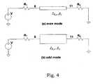
- FIG. 4shows a microstrip transmission line circuit for even and odd modes.
- the simplified circuitis only a transmission line circuit with a load for both even and odd modes, with different transmission line characteristic impedances and propagation constants.
- the effective relative dielectric constantsvary between the dielectric constants of air ( ⁇ 0 ) and the substrate ( ⁇ 1 ). Since the even mode propagates between the microstrip line and the ground, the relative effective dielectric constant for even mode will be larger than that of the odd mode. The odd mode will propagate between the two microstrip conductors.
- Equation 15states the relation of various dielectric constants ⁇ 0 ⁇ ⁇ eff , o ⁇ ⁇ eff , e ⁇ ⁇ 1
- Equation 15An implication of Equation 15 is that even mode propagates slower than the odd mode ( ⁇ e > ⁇ o ).
- the even mode impedanceis the largest impedance.
- FIG. 5a, 5b and 5cshow the port1 and port2 voltages for even and odd modes.
- Equations 1, 2, 9 and 10we can calculate the voltage waveforms at four ports. If we apply the voltage from the port1 and terminate all other ports with matched load, we can solve the circuits with their characteristic impedances and propagation constants to obtain the other port voltages.
- FIG. 6a, 6b, 6c and 6dshow the port voltages for port1 (8), port2 (9), port3 (10) and port4 (11) respectively.
- the output of interestis the monopulse from port3, which has a zero frequency component.
- FIG. 6cis the plot of the monopulse output from the MCL port3.
- this porttwo pulses with opposite polarities arrive at different times, these pulses are exact copies of the input pulse. It is the definition of derivative such that if you take one waveform and its delayed version and subtract from each other, the derivative of the waveform is obtained. Basically, this circuit does exactly that. The relative arrival time of these two pulses can be adjusted by changing the transmission line length or the dielectric constant of the substrate material.
- the voltage at port4is a two pulse waveform with the same polarities. For all 4-port voltages, there will be no more reflections even if the time axis is extended since each port is terminated with a matched load.
- FIG. 7show two schematics on Agilent ADS design software.
- One of the schematicsis that the MCL circuit connected to a pulse generator with all ports matched with 50 Ohms that is shown in FIG. 7a .
- Both circuitsare connected to a pulse generating circuit which outputs a 1-V pulse with 50 psec rise and fall times and a width of 100 psec, total pulse duration is set to 200 psec.
- the MCL circuitis designed such that a 300 psec pulse will be the output from port 3 of the circuit.
- the length of the microstrip transmission lines (2,3)can be set according to the desired pulse width of the waveform. By adjusting the transmission line length, the desired pulse shape could be obtained.
- pulse width and the transmission line lengthshould be both taken into consideration as design parameters. Basically, the odd mode and even mode propagate at different velocities, and this difference in velocities will create the time difference between the even and odd mode pulses at a specific point on the transmission line. So, for the desired pulse, the transmission line length should be a design parameter as well as the time duration of the pulse.
- Equation 17the calculated values of effective dielectric constants for the odd and even modes are given in Equation 17, and if the desired pulse width is taken as 200 picoseconds, then, the transmission line length is calculated as 25.1 cm using Equation 23. Note that for a higher dielectric constant material and by using meander trace line, the area of the transmission line circuit could be made a few square-cm.
- FIGS. 8is the plot of the zero-frequency outputs of the differentiator circuit.
- FIG. 8a and 8bshow the time domain waveform and the frequency response of the port3 voltage for a microstrip coupled line circuit according to the present invention.
- FIG. 8c and 8dshow the time domain waveform and the frequency response of the port3 voltage for a RC circuit according to the prior art UWB waveform generator. It can be seen that the pulse V3 obtained from the MCL circuit according to the present invention is well shaped and smooth, its amplitude changes between ⁇ 0.5 V, and the second order reflections are very small. Pulse envelope smoothness is important since it will determine the spurious response in the frequency domain such as sidelobe levels.
- the ultra wideband waveform generator circuitIn the ultra wideband waveform generator circuit according to the present invention, we do have smaller second order reflections and said matched loads R 1 (4), R 2 (5), R 3 (6), R 4 (7) terminating the corresponding ports (8, 9, 10, 11) reduces to zero the second order reflections of the waveform generator circuit (1) according to the present invention. This is very important if the circuit is to be used in a receiver for determining a radar return typically a small amplitude signal. If the second order reflections of the circuitry are small, then the signal sensitivity of the circuit will increase, and be able to detect smaller amplitude signals. It will also result in higher signal to interference level, and smaller distortion. Therefore, the microstrip coupled line, ultra wideband waveform generator circuit according to the present invention can be advantageously used in radars, preferably in ground penetrating radars.
- the microstrip coupled line, ultra wideband waveform generator circuit of the present inventioncan also be used in UWB communication transmitter and receiver circuits, wireless personal area networks (WPAN).
- WPANwireless personal area networks
- said microstrip coupled line, ultra wideband waveform generator circuitcan be used as an input by another circuit.
- the load impedancewill change the voltage waveform of the RC circuit output.
- connecting a load to MCLhas already been done by terminating the port3 by a matched load.
- the pulse width generated by the MCLis narrower than the RC circuit, which might be desirable for some applications.
- the use of said microstrip coupled line UWB waveform generator circuitis not only limited to generate the two opposite polarity pulses given a single pulse as described so far.
- One of these single pulsescan also be obtained by the exact MCL circuit. If a unit step pulse is applied as an input to port1, port3 output will be the monopulse waveform with narrow time duration.
- the unit step pulsecould be easily obtained from a step recovery diode, or a tunnel diode circuit. Further, the same circuit can be used to obtain Gaussian doublets from Gaussian monopulse by adding the monopulse and its delayed replica with opposite polarity.
Landscapes
- Engineering & Computer Science (AREA)
- Computer Networks & Wireless Communication (AREA)
- Signal Processing (AREA)
- Physics & Mathematics (AREA)
- Nonlinear Science (AREA)
- Dc Digital Transmission (AREA)
- Radar Systems Or Details Thereof (AREA)
Description
- The present invention relates to a novel ultra wideband (UWB) waveform generator circuit.
- UWB signal is defined as the signal that has the bandwidth to center frequency ratio greater than 0.25 or bandwith of 500 MHz or greater. In the past, UWB technology has found military applications in ground penetrating radars (GPR), wall penetrating radars, secure communications and precision positioning/trackings. However, nowadays there is also a growing interest in commercial use of UWB technology such as in Wireless Personal Area Networks (WPAN). FCC recently allocated the frequency range from 3.1 to 10.6 GHz for UWB communications.
- This interest has been the result of increasing demand for much higher data rates on the order of hundreds of megabits, since future wireless networks requires very large transmission bandwidths to reach these data rates. Currently, most wireless data technologies such as Bluetooth, IEEE 802.11b have baseband signals up to tens of megabits, and the baseband signal is sent using an RF carrier, which is basically a narrowband communication technique.
- There are mainly two alternative ways of UWB systems from the point of view of generating the UWB signal. One system is the so called the impulse radio, in which ultra narrow pulses with durations of picoseconds are generated and the generated time pulses may span a few GHz wide bandwidth. The other system is the multibanded approach so that multiple narrowband signals are generated independently and then combined to form the larger bandwidth of UWB signal.
- For time domain impulses, there exist different waveforms that can be used for UWB signal such as Gaussian monopulse, Gaussian doublets, Rayleigh, Laplacian, wavelet monopulses, etc. Each of these waveforms can be designed for a specific center frequency and a required bandwidth. The frequency domain parameters of the pulses can be derived by the time domain parameters of the pulses, and vice versa.
- Specifically, time duration of the pulse determines the frequency bandwidth occupied by the signal, the cycles per pulse. In other words, number of zero crossings determines the center frequency of the pulse and the pulse shape will provide the sidelobe levels of the signal as well as how the signal energy is distributed over the range of frequency bandwidth.
FIG. 1 shows the time domain waveform of an UWB monopulse for a duration of 400 picoseconds. This ideal Gaussian doublet is obtained as a derivative of a Gaussian waveform which is given by the following formula:
where r (tau) is the time duration of the pulse chosen as r =100psec .FIG. 2 shows the plot of the Gaussion monopulse waveform in frequency domain, wherein the center frequency of the Gaussion monopulsefc can be estimated as 2.7 GHz, which is determined by the number of zero crossings in total duration of the monopulse, τ . The 3-dB bandwidth is about 2.5 GHz, which is given as the inverse of the total duration of the pulse1/τ. The envelope of the monopulse will determine how thetotal power of the monopulse will be distributed over the ultra wideband frequency bandwidth of the monopulse.- The UWB pulse is centered around a center frequency with an ultra wide bandwidth. In other words, the single pulse may have a very large bandwidth. However, if it is centered around the zero-frequency, the design of one compact antenna for all frequencies would be very difficult. This is due to the fact that for an efficient radiator at low frequencies, antenna size should be comparable to the wavelength, which is enormously large at low frequencies.
- One way to obtain such kind of a pulse and eliminate the antenna size problem, is to first generate the zero-frequency centered pulse, then take the derivative of the pulse to eliminate the constant or DC part of the pulse and shift the center frequency from zero to a higher frequencyfc.
- Various designs of ultra wideband waveform generators are known in the art.
- An example of such UWB waveform generator circuits is disclosed inBUCHEGGER, Thomas et al. "A Novel low-cost ultra wideband microstrip pulse forming network for gaussian monocycle generation." 2003 International Workshop on Ultra Wideband Systems (IWUWBS). In this pulse forming network, microstrip lines with a short circuit termination was used to obtain the gaussian monocycle. However, with this approach there is a large ringing at the output.
- Another example of such UWB waveform generator circuits is disclosed inHAN, Jeongwoo, et al. "A New ultra-wideband, ultra-short monocycle pulse generator with reduced ringing." IEEE Microwave and Wireless Component Letters. June 2002, vol.12,no.6, p.206-208. Han et. al use Step Recovery diode and short circuited transmission line to obtain the pulse and a simple RC filter to take the derivative. However, with this approach the pulse envelope properties are degraded which results in shape distortion in frequency domain and the amplitude of the pulse is lower due to the resistance loss.
- A further example of such UWB waveform generator circuits is disclosed inLee J S et al. "New Uniplanar subnanosecond monocycle pulse generator and transformer for time-domain microwave applications" IEEE Transactions on Microwave Theory and Techniques, vol.49, no. 6, June 2001, pages 1126-1129. In this pulse generator, a step recovery diode is used to obtain a sharp edge and then this sharp edge Is converted Into a narrow pulse using a short circuited microstrip line, and then a pulse shaping network is used to further shape the pulse. However, this circuit has multiple reflections causing ringing of the signal.
- Another example of such UWB waveform generator circuits is disclosed inLow Z N et al "Novel low cost higher order derivative Gaussian pulse genarator circuit" Communication Systems, 2004. ICCS 2004. The Ninth International Conference on Singapore, China 6-8 Sept. 2004, Piscataway, NJ, USA, IEEE, pages 30-34. This pulse generator circuit uses a fast switching diode and a microstrip reflection network to obtain an UWB pulse which is a higher order Gaussian pulses. If this circuitry Is to be used for a first order derivative signal, the ringing levels will be very high which will be unacceptable to be used for UWB pulse generation. Again, there Is a high ringing level due to the use of microstrip line with short circuit termination.
US 2005/105637 A1 which is considered to be the closest prior art discloses a bi-phase modulator for UWB waveforms uses a symmetrical transformation device and a selector device to produce bi-phass modulated UWB waveforms in response to an information signal. The symmetrical transformation device receives an input UWB waveform and produces equal but opposite polarity output waveforms. The selector device determines whether an inverted or non-inverted UWB waveform is output in response to the information signal. This circuit does not create the derivative of the signal, but generates positive and negative of the input pulse, which are not the same thing with even and odd mode propagations. Moreover to generate an UWB waveform this circuit uses three serially coupled transmission lines of any type whereas the circuit of the present invention uses a single microstrip coupled line (MCL). Finally this circuit uses tapered lines for Impedance matching whereas the circuit of the present invention Is terminated by direct reference impedances.- Thus, there is a need for an UWB waveform generator circuit that can produce smooth and well-shaped pulses and achieve minimum losses in the resultant amplitude of the pulse and especially produce very small second order reflections also known as ringing. This is very important if the UWB waveform generator circuit is to be used in a receiver for determining a radar return typically a small amplitude signal.
- The invention has been proposed in view of the related art problems and aims at providing an UWB waveform generator circuit placed on a substrate with transmission lines, loads and ports; the circuit takes as input a waveform and generates as output the derivative of said waveform; the improvement being that the circuit has two microstrip transmission lines and that these lines are coupled.
- The loads match with the characteristic impedances of the microstrip transmission lines. These matched loads terminate the corresponding ports.
- UWB waveform generator circuit according to the present invention generates the derivative of the waveform using the even and odd mode propagations on the microstrip transmission lines.The length of the microstrip transmission lines can be set according to the desired pulse width of the waveform.
- The UWB waveform generator circuit according to the present invention can be used in applications chosen from: UWB communication transmitter and receiver circuits, wireless personal area networks (WPAN), radars, preferably ground penetrating radars, Thru-wall imaging radars.
- A microstrip coupled line, UWB waveform generator circuit in accordance with the present invention will now be described, by way of example only, with reference to the accompanying drawings in which:
FIG. 1 shows the time domain waveform of a UWB monopulse for a duration of 400 picoseconds,FIG. 2 shows the plot of the Gaussian monopulse waveform in frequency domain,FIG. 3a shows a microstrip coupled line, UWB waveform generator circuit according to the present invention,FIG. 3b and 3c show a microstrip coupled line UWB waveform generator circuit according to the present invention for even and odd modes respectively,FIG. 4 shows a microstrip transmission line circuit according to the present invention for even and odd modes,FIG. 5a, 5b and 5c show the port1 and port4 pulse voltages for even and odd modes,FIG. 6a, 6b and 6c show the port voltages for port1, port2, port3 and port4, respectively,FIG. 7a shows a microstrip coupled line circuit according to the present invention on Agilent ADS design software,FIG. 7b shows a RC circuit according to the prior art UWB waveform generator on Agilent ADS design software,FIG. 8a and 8b show the time domain waveform and the frequency response of the port3 voltage for a microstrip coupled line circuit according to the present invention,FIG. 8c and 8d show the time domain waveform and the frequency response of the port3 voltage for a RC circuit according to the prior art UWB waveform generator.FIGURE 3a shows an UWB waveform generator circuit (1), with transmission lines (2,3), loads R1(4), R2(5), R3(6) and R4(7) and ports (8, 9, 10, 11). Said circuit (1) takes as input a waveform and generates as output the derivative of said waveform. The circuit (1) has two microstrip transmission lines (2,3) and these lines (2,3) are coupled.- For the microstrip implementation of the circuit (1), the microstrip transmission lines (2,3) are placed on a substrate. The length of the microstrip transmission lines (2,3) can be set according to the desired pulse width of the waveform.
- The loads R1(4), R2 (5), R3 (6) and R4 (7) match with the characteristic impedances of the microstrip transmission lines (2,3). These matched loads R1(4), R2 (5), R3 (6) and R4 (7) terminate the corresponding ports (8, 9, 10, 11).
- The input is applied from port1 (8) and depending of the length of the microstrip coupled transmission lines (2, 3), the output is either from port 3 (10) or port4 (11). The circuit (1) is formed by a finite length of the coupled transmission lines (2, 3) and generates the derivative of the waveform from the even and odd mode propagations on the microstrip transmission lines (2,3).
- The analysis of the UWB waveform generator circuit (1) can be obtained using even, odd mode analysis. Since there are 3 conducting parts in the coupled microstrip line (2 microstrip conductors and a ground plane), even mode propagates between the conductors and the ground plane, and the odd mode propagates between two strip conductors.
- The circuits in
FIG. 3b and 3c show the even and odd mode propagation circuits. After solving for even and odd mode circuits, the total solution can be written as the sum of these solutions. It can be noticed fromFIG. 3b and 3c that for the even mode, the polarity of the applied voltages at port1 (8) and port2 (9) are the same, whereas, for the odd mode analysis, the polarities are reversed for port1 (8) and port2 (9). - When even and odd mode voltages are added in
FIG. 3b and 3c , 2 volts is obtained for port1 and 0 volts is obtained for port2, which are the voltages inFIG. 3a . It is also noted that the propagation constants, β0,o and β0,e, the characteristic impedances,Z0,o andZ0,e are different for even and odd modes. The total voltages at ports are given as


whereVi,e andVi,o are the even and odd mode voltages for porti. The Microstrip coupled line (MCL) circuit according to the invention can be further simplified by using the symmetry of the circuits as follows;


FIG. 4 shows a microstrip transmission line circuit for even and odd modes. The simplified circuit is only a transmission line circuit with a load for both even and odd modes, with different transmission line characteristic impedances and propagation constants. Now, the voltages can be rewritten in terms of onlyV1,e, V1,o andV4,e , V4,o and substituting Equations (5)-(8) in Equations (3) and (4), the modified equations forV2 andV3 are as follows;

- The equations for characteristic impedances and the propagation constants for even and odd modes are given by


whereR0 is the characteristic impedance of the uncoupled microstrip line and C is the coupling coefficient. Note that the geometric mean ofZ0,e andZ0,o isR0 and for positive values ofC , the even mode characteristic impedanceZ0,e is greater than the odd mode characteristic impedanceZ0,o (Z0,e >R0 >Z0,o). The propagation constants for the even and odd modes are given by

where λ0 is the free space wavelength andεeff,e andεeff,o are the relative effective dielectric constants of the even and odd mode propagation, respectively. The effective relative dielectric constants vary between the dielectric constants of air (ε0) and the substrate (ε1). Since the even mode propagates between the microstrip line and the ground, the relative effective dielectric constant for even mode will be larger than that of the odd mode. The odd mode will propagate between the two microstrip conductors. Equation 15 states the relation of various dielectric constants
- An implication of
Equation 15 is that even mode propagates slower than the odd mode (βe >βo). - For example we will consider an example of a MCL circuit, which in no way restricts the scope of the invention and we will obtain the output zero-frequency monopulse using the simple transmission line theory and also using Agilent ADS software.
- As MCL, a thickness ofh = 1.55mm and εr = 4.6 (FR4 substrate) can be chosen. The width of the microstrip transmission lines are w = 2.54mm and the separation between these lines is chosen asS = 0.508mm. Using these parameters, ADS line calculator tool, the following characteristic impedances are easily obtained;

- The even mode impedance is the largest impedance. The relative effective dielectric constants are calculated as

- It is clear from these results that the odd mode moves faster and that its characteristic impedance is smaller than that of the even mode.
FIG. 5a, 5b and 5c show the port1 and port2 voltages for even and odd modes. Using the circuits inFIG. 3b and 3c , andEquations 
- If a pulse is sent at timet =t0 seconds, the first reflection will arrive at port1 at timet =t1 seconds with smaller amplitude as shown in
FIG. 5a . For the even mode circuit,R0 is smaller thanZ0,e, and hence, a negative reflection will be from both the load and the generator side. The voltage reflection coefficient for both end of the transmission line will be given by
- If the pulse is sent at timet =t0 seconds, the first reflection will reach the port1 at timet = t2 seconds with also smaller amplitude as shown in
FIG. 5b . If the transmission line is assumed to be non-dispersive, then, odd and even mode voltages for port4 will be the time delayed versions of corresponding port1 voltages. Further, they would be delayed according to their phase velocity on the transmission line. Odd voltage pulse will arrive earlier as shown inFIG. 5c , since it travels faster. We can obtain the voltages atports Equations FIG. 6a, 6b, 6c and 6d show the port voltages for port1 (8), port2 (9), port3 (10) and port4 (11) respectively. From the point of UWB communication, the output of interest is the monopulse from port3, which has a zero frequency component. The initial pulse is applied from port1 as a 2 Volts amplitude pulse, and the reflected pulses arrive att =t1 andt =t2 seconds with much smaller amplitudes as shown inFIG. 6a . The port2 only have reflections att =t1 andt =t2 seconds as shown inFIG. 6b .FIG. 6c is the plot of the monopulse output from the MCL port3. For this port, two pulses with opposite polarities arrive at different times, these pulses are exact copies of the input pulse. It is the definition of derivative such that if you take one waveform and its delayed version and subtract from each other, the derivative of the waveform is obtained. Basically, this circuit does exactly that. The relative arrival time of these two pulses can be adjusted by changing the transmission line length or the dielectric constant of the substrate material. Finally, the voltage at port4 is a two pulse waveform with the same polarities. For all 4-port voltages, there will be no more reflections even if the time axis is extended since each port is terminated with a matched load.FIG. 7 show two schematics on Agilent ADS design software. One of the schematics is that the MCL circuit connected to a pulse generator with all ports matched with 50 Ohms that is shown inFIG. 7a . Second, the simple RC circuit according to the prior art UWB waveform generator according to J. Han et al. with C=1 pF and R = 50 Ohms is shown inFIG. 7b . Both circuits are connected to a pulse generating circuit which outputs a 1-V pulse with 50 psec rise and fall times and a width of 100 psec, total pulse duration is set to 200 psec. The MCL circuit is designed such that a 300 psec pulse will be the output fromport 3 of the circuit.- The length of the microstrip transmission lines (2,3) can be set according to the desired pulse width of the waveform. By adjusting the transmission line length, the desired pulse shape could be obtained. To obtain the desired monopulse with no zero-frequency component, pulse width and the transmission line length should be both taken into consideration as design parameters. Basically, the odd mode and even mode propagate at different velocities, and this difference in velocities will create the time difference between the even and odd mode pulses at a specific point on the transmission line. So, for the desired pulse, the transmission line length should be a design parameter as well as the time duration of the pulse. To obtain a monopulse, the difference between time delays (t2 -t1) should be equal to the pulse widthΔt. This is given by

- Assume that the length of the transmission line isl, then, the time duration that it takes for the odd and even mode voltages to reach
port 3 will be given by,

where

- Using Equations 20-22, we can obtain the transmission line length versus pulse width relation as,

- As an example, for the same FR4 substrate of εr = 4.6, the calculated values of effective dielectric constants for the odd and even modes are given in Equation 17, and if the desired pulse width is taken as 200 picoseconds, then, the transmission line length is calculated as 25.1 cm using Equation 23. Note that for a higher dielectric constant material and by using meander trace line, the area of the transmission line circuit could be made a few square-cm.
FIGS. 8 is the plot of the zero-frequency outputs of the differentiator circuit.FIG. 8a and 8b show the time domain waveform and the frequency response of the port3 voltage for a microstrip coupled line circuit according to the present invention.FIG. 8c and 8d show the time domain waveform and the frequency response of the port3 voltage for a RC circuit according to the prior art UWB waveform generator. It can be seen that the pulse V3 obtained from the MCL circuit according to the present invention is well shaped and smooth, its amplitude changes between ± 0.5 V, and the second order reflections are very small. Pulse envelope smoothness is important since it will determine the spurious response in the frequency domain such as sidelobe levels. To obtain a comparable solution, 1 pF capacitance is used in RC circuit, but, in practice, it is a very small capacitance (almost parasitic capacitances in most applications) to work with. As it can be seen fromFIG. 8c , the amplitude of waveform V6 changes between around ± 0.6 Volts, however, the waveform has very abrupt changes at its peaks, and this will increase the out of band spurious radiation. RC circuit generated pulse could be made more smooth by decreasing the capacitance values, however, this is first not that feasible since the capacitance level is already at parasitic capacitances level in a typical circuit, and also, decreasing the capacitance will also decrease the output voltage level and hence the power level.- In the prior art UWB waveform generator disclosed by J. Han et al. mentioned above, the peak voltage started as 7 Volts, and at the end of the diode, the output was measured as 1 volts. If MCL is used to obtain the monopulse voltage, the voltage drop between input and output is almost close to ideal case. We have only 3 dB loss from the generator, and this is maximum that can be drawn from the generator.
- In the ultra wideband waveform generator circuit according to the present invention, we do have smaller second order reflections and said matched loads R1 (4), R2 (5), R3 (6), R4 (7) terminating the corresponding ports (8, 9, 10, 11) reduces to zero the second order reflections of the waveform generator circuit (1) according to the present invention. This is very important if the circuit is to be used in a receiver for determining a radar return typically a small amplitude signal. If the second order reflections of the circuitry are small, then the signal sensitivity of the circuit will increase, and be able to detect smaller amplitude signals. It will also result in higher signal to interference level, and smaller distortion. Therefore, the microstrip coupled line, ultra wideband waveform generator circuit according to the present invention can be advantageously used in radars, preferably in ground penetrating radars.
- The microstrip coupled line, ultra wideband waveform generator circuit of the present invention can also be used in UWB communication transmitter and receiver circuits, wireless personal area networks (WPAN).
- According to another embodiment of the present invention, said microstrip coupled line, ultra wideband waveform generator circuit can be used as an input by another circuit. In that case, the load impedance will change the voltage waveform of the RC circuit output. However, connecting a load to MCL has already been done by terminating the port3 by a matched load. In addition, the pulse width generated by the MCL is narrower than the RC circuit, which might be desirable for some applications.
- According to still another embodiment of the present invention, the use of said microstrip coupled line UWB waveform generator circuit is not only limited to generate the two opposite polarity pulses given a single pulse as described so far. One of these single pulses can also be obtained by the exact MCL circuit. If a unit step pulse is applied as an input to port1, port3 output will be the monopulse waveform with narrow time duration. The unit step pulse could be easily obtained from a step recovery diode, or a tunnel diode circuit. Further, the same circuit can be used to obtain Gaussian doublets from Gaussian monopulse by adding the monopulse and its delayed replica with opposite polarity.


Claims (7)
- An UWB waveform generator circuit (1) placed on a substrate, with transmission lines, loads and ports wherein the circuit takes as input a waveform and generates as output the derivative of said waveform,characterized in that the circuit comprises two microstrip transmission lines that are coupled to form a microstrip coupled line (MCL)
- An UWB waveform generator circuit (1) according to claim 1,characterised in that the loads match with characteristic impedances of the micro strip coupled line (MCL).
- An UWB waveform generator circuit (1) according to claim 2,characterised in that said matched loads terminate corresponding ports.
- An UWB waveform generator circuit (1) according to any one of the preceding claims,characterised in that it generates the derivative of the waveform from the even and odd mode propagations on the micro strip coupled line (MCL)
- An UWB waveform generator circuit (1) according to any one of the preceding claims,characterised in that the length of the microstrip coupled line (MCL) can be set according to the desired pulse width of the waveform.
- An UWB waveform generator circuit (1) according to any one of the preceding claims for use in applications chosen from: UWB communication transmitter and receiver circuits, wireless personal area Networks (WPAN) and radars.
- An UWB waveform generator circuit (1) according to claim 6,characterised in that its use in radar applications are in ground penetrating radars and Thru-Wall Imaging Radars.
Priority Applications (3)
| Application Number | Priority Date | Filing Date | Title |
|---|---|---|---|
| EP05404001.9AEP1739849B1 (en) | 2005-06-30 | 2005-06-30 | A novel ultra wideband waveform generator circuit |
| US11/452,598US7864870B2 (en) | 2005-06-30 | 2006-06-14 | Ultra wideband waveform generator circuit |
| JP2006182241AJP4889383B2 (en) | 2005-06-30 | 2006-06-30 | Ultra-wideband waveform generator |
Applications Claiming Priority (1)
| Application Number | Priority Date | Filing Date | Title |
|---|---|---|---|
| EP05404001.9AEP1739849B1 (en) | 2005-06-30 | 2005-06-30 | A novel ultra wideband waveform generator circuit |
Publications (2)
| Publication Number | Publication Date |
|---|---|
| EP1739849A1 EP1739849A1 (en) | 2007-01-03 |
| EP1739849B1true EP1739849B1 (en) | 2015-09-16 |
Family
ID=35311903
Family Applications (1)
| Application Number | Title | Priority Date | Filing Date |
|---|---|---|---|
| EP05404001.9AExpired - LifetimeEP1739849B1 (en) | 2005-06-30 | 2005-06-30 | A novel ultra wideband waveform generator circuit |
Country Status (3)
| Country | Link |
|---|---|
| US (1) | US7864870B2 (en) |
| EP (1) | EP1739849B1 (en) |
| JP (1) | JP4889383B2 (en) |
Families Citing this family (6)
| Publication number | Priority date | Publication date | Assignee | Title |
|---|---|---|---|---|
| US9590603B1 (en) | 2007-08-31 | 2017-03-07 | Louisiana Tech Research Corporation | Beam steerable UWB radar |
| WO2009029819A1 (en) | 2007-08-31 | 2009-03-05 | Louisiana Tech Research Foundation; A Division Of Louisiana Tech University Foundation, Inc. | Pipe survey method using uwb signal |
| MY164860A (en)* | 2007-11-22 | 2018-01-30 | Univ Putra Malaysia | An ultra wideband pulse shaper for in band interference mitigation |
| CA2772848C (en) | 2011-03-29 | 2015-12-08 | Erez Allouche | Universal impedance probe for detection of side-connections through thermoplastic, thermosetting and cementitious liners |
| US9151837B2 (en) | 2011-09-27 | 2015-10-06 | Louisiana Tech University Research Foundation; A Division Of Louisiana Tech University Foundation, Inc. | Sensor fusion framework using multiple sensors to assess buried structures |
| CN107342787B (en)* | 2017-06-22 | 2019-07-26 | 长安大学 | An improved ultra-wideband frequency-shifted Gaussian waveform pulse design method |
Family Cites Families (19)
| Publication number | Priority date | Publication date | Assignee | Title |
|---|---|---|---|---|
| JPS6346809A (en)* | 1986-08-14 | 1988-02-27 | Yuniden Kk | Microwave mixer device |
| JPS63299504A (en)* | 1987-05-29 | 1988-12-07 | Toko Inc | Voltage controlled oscillation circuit |
| JPH02268003A (en)* | 1989-04-10 | 1990-11-01 | Matsushita Electric Ind Co Ltd | Microwave integrated circuit and microwave amplifier |
| US5345471A (en)* | 1993-04-12 | 1994-09-06 | The Regents Of The University Of California | Ultra-wideband receiver |
| WO1998004039A1 (en)* | 1996-07-19 | 1998-01-29 | Isis Innovation Limited | Transmission or delay line transformers |
| US5942950A (en)* | 1997-05-12 | 1999-08-24 | Ail Systems, Inc. | Varactor tuned strip line resonator and VCO using same |
| US6449308B1 (en)* | 1999-05-25 | 2002-09-10 | Intel Corporation | High-speed digital distribution system |
| JP2001257509A (en)* | 2000-03-14 | 2001-09-21 | Hitachi Electronics Eng Co Ltd | Micro strip line |
| US6956653B1 (en)* | 2000-06-27 | 2005-10-18 | Lockheed Martin Corporation | Dual electrooptic waveguide interferometer |
| US7248148B2 (en)* | 2000-08-09 | 2007-07-24 | Current Technologies, Llc | Power line coupling device and method of using the same |
| JP2004040259A (en)* | 2002-06-28 | 2004-02-05 | Fujitsu Quantum Devices Ltd | Directional coupler and electronic apparatus employing the same |
| AU2003270417A1 (en)* | 2002-09-09 | 2004-03-29 | Robertshaw Industrial Products Division | Interface detection using time domain reflectometry with two separate conductive elements |
| US20050105637A1 (en) | 2003-11-14 | 2005-05-19 | Fitzpatrick Douglas D. | Bi-phase modulator for ultra wideband signals |
| JP2005217926A (en)* | 2004-01-30 | 2005-08-11 | Samsung Yokohama Research Institute Co Ltd | UWB communication apparatus and UWB communication method |
| JP2006074679A (en)* | 2004-09-06 | 2006-03-16 | Futaba Corp | Ultra wideband radio transmitting apparatus, ultra wideband radio receiving apparatus, and ultra wideband radio transmitting/receiving system |
| US7469131B2 (en)* | 2004-09-14 | 2008-12-23 | Nokia Corporation | Terminal and associated transducer assembly and method for selectively transducing in at least two frequency bands |
| US7535337B2 (en)* | 2004-11-18 | 2009-05-19 | Goliath Solutions, Llc | Systems and methods for monitoring open stock merchandising |
| US7256727B2 (en)* | 2005-01-07 | 2007-08-14 | Time Domain Corporation | System and method for radiating RF waveforms using discontinues associated with a utility transmission line |
| US9118216B2 (en)* | 2005-02-18 | 2015-08-25 | Cpg Technologies, Llc | Parametric power multiplication |
- 2005
- 2005-06-30EPEP05404001.9Apatent/EP1739849B1/ennot_activeExpired - Lifetime
- 2006
- 2006-06-14USUS11/452,598patent/US7864870B2/ennot_activeExpired - Fee Related
- 2006-06-30JPJP2006182241Apatent/JP4889383B2/ennot_activeExpired - Fee Related
Also Published As
| Publication number | Publication date |
|---|---|
| JP4889383B2 (en) | 2012-03-07 |
| JP2007053737A (en) | 2007-03-01 |
| EP1739849A1 (en) | 2007-01-03 |
| US7864870B2 (en) | 2011-01-04 |
| US20070002930A1 (en) | 2007-01-04 |
Similar Documents
| Publication | Publication Date | Title |
|---|---|---|
| US7864870B2 (en) | Ultra wideband waveform generator circuit | |
| CN105137448A (en) | Ultra-wide-band all-optical radar system covering all wavebands | |
| Li et al. | Time-domain characterization of short-pulse networks and antennas using signal space method | |
| Miao et al. | On the development of an integrated CMOS-based UWB tunable-pulse transmit module | |
| US8355453B2 (en) | UWB transmitter | |
| Pozar | Closed-form approximations for link loss in a UWB radio system using small antennas | |
| US20090080493A1 (en) | Apparatus and method for generating a monocycle | |
| Yilmaz et al. | Ultra-wideband n-bit digitally tunable pulse generator | |
| Fan et al. | Source pulse optimizations for UWB radio systems | |
| Wang et al. | Time-varying matching networks for signal-centric systems | |
| US8248125B1 (en) | RF microwave circuit and pulse shaping method | |
| CN101540596B (en) | Picosecond Pulse Generator Based on Coplanar Waveguide | |
| Rahman et al. | A picosecond ultrafast pulse generation featuring switchable operation between monocycle and doublet pulses | |
| Valizade Shahmirzadi et al. | Design of reconfigurable active integrated pulse generator‐antenna with pulse‐shape modulation for ultra‐wideband applications | |
| Tekin | UWB microstrip filter design using a time‐domain technique | |
| Tekin | Ultra wideband pulse generation using microstrip coupled lines | |
| Ju et al. | Design and implementation of a hybrid digital and RF front‐end module for 24‐GHz intelligent transport system pulse‐doppler radar | |
| Ma et al. | An impulse-radio-based ultrawideband RF front-end module with a new multilayered microwave sampler | |
| Han et al. | A multipulse transmitter for UWB radar and communication systems | |
| CN101527541B (en) | Picosecond pulse generator based on coplanar waveguide and trough line | |
| Mollfulleda et al. | Ultra-wideband testbed for reduced data-rates and location | |
| Sapkal et al. | Ultra wideband monocycle pulse generation using SRD and coupled line band pass filter with reduced ringing level | |
| Guan et al. | A 0.25-/spl mu/m CMOS ultra-wideband amplifier for time-domain UWB applications | |
| Chernogor et al. | Dispersive distortions of the fractal ultra-wideband signals in plasma media | |
| Cao et al. | An Ultra-wideband Adjustable Pulse Generator Design |
Legal Events
| Date | Code | Title | Description |
|---|---|---|---|
| PUAI | Public reference made under article 153(3) epc to a published international application that has entered the european phase | Free format text:ORIGINAL CODE: 0009012 | |
| AK | Designated contracting states | Kind code of ref document:A1 Designated state(s):AT BE BG CH CY CZ DE DK EE ES FI FR GB GR HU IE IS IT LI LT LU MC NL PL PT RO SE SI SK TR | |
| AX | Request for extension of the european patent | Extension state:AL BA HR LV MK YU | |
| 17P | Request for examination filed | Effective date:20070626 | |
| AKX | Designation fees paid | Designated state(s):AT BE BG CH CY CZ DE DK EE ES FI FR GB GR HU IE IS IT LI LT LU MC NL PL PT RO SE SI SK TR | |
| 17Q | First examination report despatched | Effective date:20100906 | |
| GRAP | Despatch of communication of intention to grant a patent | Free format text:ORIGINAL CODE: EPIDOSNIGR1 | |
| RIC1 | Information provided on ipc code assigned before grant | Ipc:H04B 1/719 20110101ALN20150410BHEP Ipc:H04B 1/717 20110101AFI20150410BHEP Ipc:H03K 5/06 20060101ALI20150410BHEP | |
| INTG | Intention to grant announced | Effective date:20150428 | |
| GRAS | Grant fee paid | Free format text:ORIGINAL CODE: EPIDOSNIGR3 | |
| REG | Reference to a national code | Ref country code:DE Ref legal event code:R079 Ref document number:602005047495 Country of ref document:DE Free format text:PREVIOUS MAIN CLASS: H04B0001690000 Ipc:H04B0001717000 | |
| GRAP | Despatch of communication of intention to grant a patent | Free format text:ORIGINAL CODE: EPIDOSNIGR1 | |
| GRAA | (expected) grant | Free format text:ORIGINAL CODE: 0009210 | |
| RIC1 | Information provided on ipc code assigned before grant | Ipc:H04B 1/717 20110101AFI20150715BHEP Ipc:H03K 5/06 20060101ALI20150715BHEP Ipc:H04B 1/719 20110101ALN20150715BHEP | |
| INTG | Intention to grant announced | Effective date:20150727 | |
| AK | Designated contracting states | Kind code of ref document:B1 Designated state(s):AT BE BG CH CY CZ DE DK EE ES FI FR GB GR HU IE IS IT LI LT LU MC NL PL PT RO SE SI SK TR | |
| REG | Reference to a national code | Ref country code:GB Ref legal event code:FG4D | |
| REG | Reference to a national code | Ref country code:CH Ref legal event code:EP | |
| REG | Reference to a national code | Ref country code:IE Ref legal event code:FG4D | |
| REG | Reference to a national code | Ref country code:AT Ref legal event code:REF Ref document number:750514 Country of ref document:AT Kind code of ref document:T Effective date:20151015 | |
| REG | Reference to a national code | Ref country code:DE Ref legal event code:R096 Ref document number:602005047495 Country of ref document:DE | |
| REG | Reference to a national code | Ref country code:NL Ref legal event code:MP Effective date:20150916 | |
| PG25 | Lapsed in a contracting state [announced via postgrant information from national office to epo] | Ref country code:LT Free format text:LAPSE BECAUSE OF FAILURE TO SUBMIT A TRANSLATION OF THE DESCRIPTION OR TO PAY THE FEE WITHIN THE PRESCRIBED TIME-LIMIT Effective date:20150916 Ref country code:GR Free format text:LAPSE BECAUSE OF FAILURE TO SUBMIT A TRANSLATION OF THE DESCRIPTION OR TO PAY THE FEE WITHIN THE PRESCRIBED TIME-LIMIT Effective date:20151217 Ref country code:FI Free format text:LAPSE BECAUSE OF FAILURE TO SUBMIT A TRANSLATION OF THE DESCRIPTION OR TO PAY THE FEE WITHIN THE PRESCRIBED TIME-LIMIT Effective date:20150916 | |
| REG | Reference to a national code | Ref country code:LT Ref legal event code:MG4D | |
| REG | Reference to a national code | Ref country code:AT Ref legal event code:MK05 Ref document number:750514 Country of ref document:AT Kind code of ref document:T Effective date:20150916 | |
| PG25 | Lapsed in a contracting state [announced via postgrant information from national office to epo] | Ref country code:SE Free format text:LAPSE BECAUSE OF FAILURE TO SUBMIT A TRANSLATION OF THE DESCRIPTION OR TO PAY THE FEE WITHIN THE PRESCRIBED TIME-LIMIT Effective date:20150916 | |
| PG25 | Lapsed in a contracting state [announced via postgrant information from national office to epo] | Ref country code:NL Free format text:LAPSE BECAUSE OF FAILURE TO SUBMIT A TRANSLATION OF THE DESCRIPTION OR TO PAY THE FEE WITHIN THE PRESCRIBED TIME-LIMIT Effective date:20150916 | |
| PG25 | Lapsed in a contracting state [announced via postgrant information from national office to epo] | Ref country code:SK Free format text:LAPSE BECAUSE OF FAILURE TO SUBMIT A TRANSLATION OF THE DESCRIPTION OR TO PAY THE FEE WITHIN THE PRESCRIBED TIME-LIMIT Effective date:20150916 Ref country code:IS Free format text:LAPSE BECAUSE OF FAILURE TO SUBMIT A TRANSLATION OF THE DESCRIPTION OR TO PAY THE FEE WITHIN THE PRESCRIBED TIME-LIMIT Effective date:20160116 Ref country code:ES Free format text:LAPSE BECAUSE OF FAILURE TO SUBMIT A TRANSLATION OF THE DESCRIPTION OR TO PAY THE FEE WITHIN THE PRESCRIBED TIME-LIMIT Effective date:20150916 Ref country code:IT Free format text:LAPSE BECAUSE OF FAILURE TO SUBMIT A TRANSLATION OF THE DESCRIPTION OR TO PAY THE FEE WITHIN THE PRESCRIBED TIME-LIMIT Effective date:20150916 Ref country code:EE Free format text:LAPSE BECAUSE OF FAILURE TO SUBMIT A TRANSLATION OF THE DESCRIPTION OR TO PAY THE FEE WITHIN THE PRESCRIBED TIME-LIMIT Effective date:20150916 Ref country code:CZ Free format text:LAPSE BECAUSE OF FAILURE TO SUBMIT A TRANSLATION OF THE DESCRIPTION OR TO PAY THE FEE WITHIN THE PRESCRIBED TIME-LIMIT Effective date:20150916 | |
| PG25 | Lapsed in a contracting state [announced via postgrant information from national office to epo] | Ref country code:RO Free format text:LAPSE BECAUSE OF FAILURE TO SUBMIT A TRANSLATION OF THE DESCRIPTION OR TO PAY THE FEE WITHIN THE PRESCRIBED TIME-LIMIT Effective date:20150916 Ref country code:PT Free format text:LAPSE BECAUSE OF FAILURE TO SUBMIT A TRANSLATION OF THE DESCRIPTION OR TO PAY THE FEE WITHIN THE PRESCRIBED TIME-LIMIT Effective date:20160118 Ref country code:AT Free format text:LAPSE BECAUSE OF FAILURE TO SUBMIT A TRANSLATION OF THE DESCRIPTION OR TO PAY THE FEE WITHIN THE PRESCRIBED TIME-LIMIT Effective date:20150916 Ref country code:PL Free format text:LAPSE BECAUSE OF FAILURE TO SUBMIT A TRANSLATION OF THE DESCRIPTION OR TO PAY THE FEE WITHIN THE PRESCRIBED TIME-LIMIT Effective date:20150916 | |
| REG | Reference to a national code | Ref country code:DE Ref legal event code:R097 Ref document number:602005047495 Country of ref document:DE | |
| PLBE | No opposition filed within time limit | Free format text:ORIGINAL CODE: 0009261 | |
| STAA | Information on the status of an ep patent application or granted ep patent | Free format text:STATUS: NO OPPOSITION FILED WITHIN TIME LIMIT | |
| 26N | No opposition filed | Effective date:20160617 | |
| PG25 | Lapsed in a contracting state [announced via postgrant information from national office to epo] | Ref country code:DK Free format text:LAPSE BECAUSE OF FAILURE TO SUBMIT A TRANSLATION OF THE DESCRIPTION OR TO PAY THE FEE WITHIN THE PRESCRIBED TIME-LIMIT Effective date:20150916 | |
| PGFP | Annual fee paid to national office [announced via postgrant information from national office to epo] | Ref country code:TR Payment date:20160418 Year of fee payment:12 | |
| PGFP | Annual fee paid to national office [announced via postgrant information from national office to epo] | Ref country code:DE Payment date:20160704 Year of fee payment:12 | |
| PG25 | Lapsed in a contracting state [announced via postgrant information from national office to epo] | Ref country code:SI Free format text:LAPSE BECAUSE OF FAILURE TO SUBMIT A TRANSLATION OF THE DESCRIPTION OR TO PAY THE FEE WITHIN THE PRESCRIBED TIME-LIMIT Effective date:20150916 | |
| PG25 | Lapsed in a contracting state [announced via postgrant information from national office to epo] | Ref country code:BE Free format text:LAPSE BECAUSE OF FAILURE TO SUBMIT A TRANSLATION OF THE DESCRIPTION OR TO PAY THE FEE WITHIN THE PRESCRIBED TIME-LIMIT Effective date:20150916 | |
| PG25 | Lapsed in a contracting state [announced via postgrant information from national office to epo] | Ref country code:MC Free format text:LAPSE BECAUSE OF FAILURE TO SUBMIT A TRANSLATION OF THE DESCRIPTION OR TO PAY THE FEE WITHIN THE PRESCRIBED TIME-LIMIT Effective date:20150916 | |
| REG | Reference to a national code | Ref country code:CH Ref legal event code:PL | |
| GBPC | Gb: european patent ceased through non-payment of renewal fee | Effective date:20160630 | |
| REG | Reference to a national code | Ref country code:IE Ref legal event code:MM4A | |
| REG | Reference to a national code | Ref country code:FR Ref legal event code:ST Effective date:20170228 | |
| PG25 | Lapsed in a contracting state [announced via postgrant information from national office to epo] | Ref country code:FR Free format text:LAPSE BECAUSE OF NON-PAYMENT OF DUE FEES Effective date:20160630 Ref country code:CH Free format text:LAPSE BECAUSE OF NON-PAYMENT OF DUE FEES Effective date:20160630 Ref country code:LI Free format text:LAPSE BECAUSE OF NON-PAYMENT OF DUE FEES Effective date:20160630 | |
| PG25 | Lapsed in a contracting state [announced via postgrant information from national office to epo] | Ref country code:GB Free format text:LAPSE BECAUSE OF NON-PAYMENT OF DUE FEES Effective date:20160630 Ref country code:IE Free format text:LAPSE BECAUSE OF NON-PAYMENT OF DUE FEES Effective date:20160630 | |
| REG | Reference to a national code | Ref country code:DE Ref legal event code:R119 Ref document number:602005047495 Country of ref document:DE | |
| PG25 | Lapsed in a contracting state [announced via postgrant information from national office to epo] | Ref country code:DE Free format text:LAPSE BECAUSE OF NON-PAYMENT OF DUE FEES Effective date:20180103 | |
| PG25 | Lapsed in a contracting state [announced via postgrant information from national office to epo] | Ref country code:HU Free format text:LAPSE BECAUSE OF FAILURE TO SUBMIT A TRANSLATION OF THE DESCRIPTION OR TO PAY THE FEE WITHIN THE PRESCRIBED TIME-LIMIT; INVALID AB INITIO Effective date:20050630 Ref country code:CY Free format text:LAPSE BECAUSE OF FAILURE TO SUBMIT A TRANSLATION OF THE DESCRIPTION OR TO PAY THE FEE WITHIN THE PRESCRIBED TIME-LIMIT Effective date:20150916 | |
| PG25 | Lapsed in a contracting state [announced via postgrant information from national office to epo] | Ref country code:LU Free format text:LAPSE BECAUSE OF NON-PAYMENT OF DUE FEES Effective date:20160630 | |
| PG25 | Lapsed in a contracting state [announced via postgrant information from national office to epo] | Ref country code:BG Free format text:LAPSE BECAUSE OF FAILURE TO SUBMIT A TRANSLATION OF THE DESCRIPTION OR TO PAY THE FEE WITHIN THE PRESCRIBED TIME-LIMIT Effective date:20150916 | |
| PG25 | Lapsed in a contracting state [announced via postgrant information from national office to epo] | Ref country code:TR Free format text:LAPSE BECAUSE OF NON-PAYMENT OF DUE FEES Effective date:20170630 |