EP1738511B1 - Wideband enhanced digital injection predistortion system and method - Google Patents
Wideband enhanced digital injection predistortion system and methodDownload PDFInfo
- Publication number
- EP1738511B1 EP1738511B1EP05722448AEP05722448AEP1738511B1EP 1738511 B1EP1738511 B1EP 1738511B1EP 05722448 AEP05722448 AEP 05722448AEP 05722448 AEP05722448 AEP 05722448AEP 1738511 B1EP1738511 B1EP 1738511B1
- Authority
- EP
- European Patent Office
- Prior art keywords
- digital
- nonlinear
- compensation circuit
- output
- envelope
- Prior art date
- Legal status (The legal status is an assumption and is not a legal conclusion. Google has not performed a legal analysis and makes no representation as to the accuracy of the status listed.)
- Expired - Lifetime
Links
- 238000000034methodMethods0.000titleclaimsdescription18
- 238000002347injectionMethods0.000title1
- 239000007924injectionSubstances0.000title1
- 238000005312nonlinear dynamicMethods0.000claimsdescription31
- 230000003068static effectEffects0.000claimsdescription25
- 230000003044adaptive effectEffects0.000claimsdescription19
- 230000003111delayed effectEffects0.000claimsdescription17
- 230000004044responseEffects0.000claimsdescription16
- 238000004891communicationMethods0.000claimsdescription11
- 230000009466transformationEffects0.000claimsdescription6
- 238000005070samplingMethods0.000claimsdescription3
- 238000001914filtrationMethods0.000claims5
- 238000001514detection methodMethods0.000claims1
- 238000010586diagramMethods0.000description16
- 230000003446memory effectEffects0.000description16
- 230000015654memoryEffects0.000description12
- 238000012545processingMethods0.000description11
- 239000000654additiveSubstances0.000description10
- 230000000996additive effectEffects0.000description10
- 238000013461designMethods0.000description9
- 238000006243chemical reactionMethods0.000description8
- 230000006870functionEffects0.000description8
- 238000012546transferMethods0.000description8
- 230000000694effectsEffects0.000description7
- 238000012937correctionMethods0.000description6
- 230000006978adaptationEffects0.000description5
- 230000008901benefitEffects0.000description5
- 230000003321amplificationEffects0.000description4
- 238000003199nucleic acid amplification methodMethods0.000description4
- 238000013139quantizationMethods0.000description3
- 230000003595spectral effectEffects0.000description3
- 230000001360synchronised effectEffects0.000description3
- 238000000844transformationMethods0.000description3
- 238000004458analytical methodMethods0.000description2
- 238000013459approachMethods0.000description2
- 230000006399behaviorEffects0.000description2
- 239000000872bufferSubstances0.000description2
- 230000001447compensatory effectEffects0.000description2
- 238000005516engineering processMethods0.000description2
- 239000011159matrix materialSubstances0.000description2
- 238000012986modificationMethods0.000description2
- 230000004048modificationEffects0.000description2
- 238000012360testing methodMethods0.000description2
- 238000010200validation analysisMethods0.000description2
- 125000000205L-threonino groupChemical group[H]OC(=O)[C@@]([H])(N([H])[*])[C@](C([H])([H])[H])([H])O[H]0.000description1
- XUIMIQQOPSSXEZ-UHFFFAOYSA-NSiliconChemical compound[Si]XUIMIQQOPSSXEZ-UHFFFAOYSA-N0.000description1
- 230000015556catabolic processEffects0.000description1
- 230000001413cellular effectEffects0.000description1
- 238000006731degradation reactionMethods0.000description1
- 230000001934delayEffects0.000description1
- 230000001419dependent effectEffects0.000description1
- 230000010339dilationEffects0.000description1
- 230000009977dual effectEffects0.000description1
- 230000036039immunityEffects0.000description1
- 230000007787long-term memoryEffects0.000description1
- 230000007774longtermEffects0.000description1
- 230000000135prohibitive effectEffects0.000description1
- 230000009467reductionEffects0.000description1
- 230000001105regulatory effectEffects0.000description1
- 238000011160researchMethods0.000description1
- 230000006403short-term memoryEffects0.000description1
- 229910052710siliconInorganic materials0.000description1
- 239000010703siliconSubstances0.000description1
- 238000001228spectrumMethods0.000description1
- 238000012795verificationMethods0.000description1
Images


Classifications
- H—ELECTRICITY
- H03—ELECTRONIC CIRCUITRY
- H03F—AMPLIFIERS
- H03F1/00—Details of amplifiers with only discharge tubes, only semiconductor devices or only unspecified devices as amplifying elements
- H03F1/32—Modifications of amplifiers to reduce non-linear distortion
- H—ELECTRICITY
- H03—ELECTRONIC CIRCUITRY
- H03F—AMPLIFIERS
- H03F1/00—Details of amplifiers with only discharge tubes, only semiconductor devices or only unspecified devices as amplifying elements
- H03F1/32—Modifications of amplifiers to reduce non-linear distortion
- H03F1/3241—Modifications of amplifiers to reduce non-linear distortion using predistortion circuits
- H03F1/3252—Modifications of amplifiers to reduce non-linear distortion using predistortion circuits using multiple parallel paths between input and output
- H—ELECTRICITY
- H03—ELECTRONIC CIRCUITRY
- H03F—AMPLIFIERS
- H03F1/00—Details of amplifiers with only discharge tubes, only semiconductor devices or only unspecified devices as amplifying elements
- H03F1/32—Modifications of amplifiers to reduce non-linear distortion
- H03F1/3241—Modifications of amplifiers to reduce non-linear distortion using predistortion circuits
- H03F1/3247—Modifications of amplifiers to reduce non-linear distortion using predistortion circuits using feedback acting on predistortion circuits
- H—ELECTRICITY
- H03—ELECTRONIC CIRCUITRY
- H03F—AMPLIFIERS
- H03F1/00—Details of amplifiers with only discharge tubes, only semiconductor devices or only unspecified devices as amplifying elements
- H03F1/32—Modifications of amplifiers to reduce non-linear distortion
- H03F1/3241—Modifications of amplifiers to reduce non-linear distortion using predistortion circuits
- H03F1/3294—Acting on the real and imaginary components of the input signal
- H—ELECTRICITY
- H03—ELECTRONIC CIRCUITRY
- H03F—AMPLIFIERS
- H03F2200/00—Indexing scheme relating to amplifiers
- H03F2200/102—A non-specified detector of a signal envelope being used in an amplifying circuit
- H—ELECTRICITY
- H03—ELECTRONIC CIRCUITRY
- H03F—AMPLIFIERS
- H03F2200/00—Indexing scheme relating to amplifiers
- H03F2200/336—A I/Q, i.e. phase quadrature, modulator or demodulator being used in an amplifying circuit
Definitions
- the present inventionis directed to predistortion linearization of high efficiency, high power RF amplifiers and related systems and methods.
- Modern wireless communication systemsemploy spectrally efficient, digitally modulated signals with wide bandwidths and time-varying envelopes. Variations in the envelope magnitude of digital modulations generate distortion components at the output of the transmitter that are caused by the inherent nonlinearity of RF amplification circuits. Amplifier distortion produces a dilation of the spectrum of the input signal ("spectral regrowth") which causes interference to communications in adjacent channels. Adjacent channel interference (ACI) is a highly undesirable phenomenon that is tightly controlled by regulatory organizations (FCC, ETSI, ITU). In addition to spectral regrowth, amplifier nonlinearities produce in-band distortion (i.e.
- Nonlinearities in conventional RF amplifiersare relatively minor (distortion approximately 40 dB below the level of the carrier for output back offs (OBO) equal to the peak-to-average power ratio (PAR) of the modulation).
- PARpeak-to-average power ratio
- High efficiency amplificationis highly desirable since it improves system reliability (longer mean time before failure (MTBF)), simplifies thermal management, reduces amplifier size (lower silicon requirements) and lowers the operational and ownership costs of base stations.
- High efficiency amplifierse.g., Doherty amplifier designs
- Class AB designsexhibit much more nonlinear behavior than Class AB designs (distortion at or less than 29 dB below the level of the carrier).
- feed forwardis based on additive post-correction of amplifier distortion, typically employing a dual loop architecture to estimate the output distortion of the amplifier in a first (carrier cancellation) loop and then injecting the distortion estimate, properly phased and scaled, to the output of the "main" amplifier via an RF auxiliary or “error” amplifier in a second (distortion cancellation) loop.
- Feed forward linearization systemsdo not suffer from the bandwidth limitations of feedback linearizers and are unconditionally stable. However, and despite having wide bandwidth distortion correction capabilities, feed forward systems usually have low efficiency due to the DC power consumption of the error amplifier and the presence of lossy delay elements at the output of the main amplifier required for phase alignment of the distortion cancellation loop.
- predistortion linearizationAn alternative technique suitable for high linearity and high efficiency amplification is predistortion linearization.
- the predistortion techniquelinearizes the amplifier by injecting a compensatory distortion component at the input of the amplifier whose phase is opposite (180 degrees out of phase) to that of the amplifier's output distortion and whose amplitude is that of the output distortion divided by the linear gain of the amplifier.
- Predistortiondoes not suffer from the stability and severe bandwidth restrictions of feedback linearization systems. It also has the advantage over back off and feed forward linearization that its application in a well designed system does not result in a severe degradation of amplifier efficiency. Due to these inherent advantages, predistortion linearization has been the subject of intense research over the past decade.
- predistortion linearizationPrior approaches to predistortion linearization have primarily focused on the design and implementation of digital LUT (Look Up Table) predistorters given the flexibility, precision and noise immunity advantages that they typically offer in comparison to analog predistorters.
- LUTLook Up Table
- predistortionis carried out in baseband in either polar or Cartesian coordinates.
- polar digital predistortion systemsa conversion between Cartesian/polar coordinates is usually necessary due to the fact that the digital input modulation is in quadrature form.
- the coefficients of the predistorterare adaptively computed and stored in tables indexed by transformations of the input (or output) signal envelopes.
- LUT predistortersare intended to only compensate for nonlinear static amplifier distortion, without provisions for the linearization of dynamic nonlinearities in the amplifier.
- These "static" predistortersare not well suited for high efficiency base station transmitter designs due to the fact that nonlinear dynamic distortion components or “memory effects" constitute a substantial portion of the total output distortion of high power, high efficiency amplifiers.
- nonparametric digital baseband predistortershave been proposed in which multidimensional tables are indexed by dynamic transformations (filtered versions) of the instantaneous input envelope magnitude or power.
- the main advantage of the multitable technique for nonlinear dynamic distortion compensationis that it does not require the computation of a parametric model of the inverse dynamics of the amplifier.
- the main disadvantagesare large memory requirements for storing the predistortion coefficients and the computational complexity involved in the interpolation of table entries when there is unreliable/insufficient data for system adaptation. Multitable interpolation complexity can be quite substantial, posing a limit to the accuracy and adaptation rate of the predistorter.
- the accuracy of digital LUT predistortersis also limited by table quantization errors.
- the present inventionis directed to overcoming the above noted shortcomings of the prior art and providing a predistortion system suitable for wide bandwidth applications without introducing undue complexity into the system.
- the present inventionprovides a digital predistorter as claimed in claim 1.
- the present inventionprovides a method for predistorting a communication signal prior to amplification by an RF amplifier as claimed in claim 10.
- the present inventionprovides a digital predistortion system and method with enhanced distortion correction capabilities.
- the present inventionfurther provides an improved predistortion linearized amplifier system and related method.
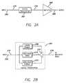
- FIGURES 1A and 1Bshow an additive predistortion system and predistortion linearized amplifier in accordance with a first embodiment of the present invention in which the distortion compensation signal is added (injected) digitally to the baseband modulation input to form the predistorted signal to drive the amplifier.
- FIGURES 2A and 2Bshow a multiplicative predistortion system and predistortion linearized amplifier in accordance with a second embodiment of the present invention in which the digital predistorter acts as a nonlinear operator in cascade with the amplifier.
- the predistortion linearized amplifier system in accordance with a first embodiment of the present inventionincludes an amplifier 100 which is preferably a high power RF amplifier of a type adapted for wireless communications applications such as cellular base stations.
- Amplifier 100may advantageously be designed to have relatively high efficiency.
- a high efficiency amplifier design employing dynamic load modulationis disclosed in US patent application serial no. 10/837,838, filed May 3, 2004 .
- amplifier 100may correspond to a conventional design operated at a lower output back off level for high efficiency.
- Other designs for amplifier 100may also be employed. Such efficient amplifier designs may introduce distortion into the amplified signal, however, especially for signal peaks.
- a digital predistortion system 102compensates for distortion introduced by amplifier 100 by predistorting an input signal applied to input 104.
- input 104may receive a digital communication signal in the form of a complex quadrature (I,Q) signal comprising a stream of signal samples which may be modulated in any of a variety of modulation schemes well known in the art.
- the input signalmay be a wideband signal such as a WCDMA multi-carrier communication signal.
- the digital predistortion systemcomprises a first signal path 120 coupled to the input 104 and a second signal path comprising a digital predistorter 108 coupled to input 104 via line 122 which operates on the input signal and provides a predistortion signal on line 124.
- An addition circuit 110is coupled to the first and second signal paths and injects the predistortion signal into the input signal and outputs a predistorted input signal on line 126.
- the signal from addition circuit 110is a baseband predistorted digital signal.
- Conventional digital to analog conversion circuitry and up conversion circuitry(shown in FIGURE 4 and discussed below) convert the predistorted digital signal to a predistorted analog RF signal.
- the amplifier 100receives and amplifies the predistorted analog RF signal and provides an amplified RF output signal on line 106 which is substantially free of distortion.
- FIGURE 1Bthe basic architecture of the digital predistortion system 102 is shown.
- the basic predistortion operation on the input signalis performed in the second signal path by digital predistorter 108.
- the predistorter 108preferably uses a polynomial model to accurately predistort the amplifier. More specifically, the predistorter preferably uses a discrete-time polynomial kernel to model the inverse transfer characteristic of the amplifier. Accurate predistortion is achieved by providing separate and simultaneous polynomial modeling and compensation for linear dynamic, nonlinear static, and nonlinear dynamic distortion as depicted in the functional diagram of FIGURE 1 B by blocks 112, 114, and 116, respectively.
- the linear dynamic block 112compensates for in-band distortion due to the amplifier 100 (and also in-band distortion due to other active components, including analog quadrature modulation errors, due to the AQM circuitry shown in FIGURE 4 ).
- the nonlinear static block 114 of the predistortercompensates for distortion due to instantaneous input signal levels, so called memoryless distortion.
- the nonlinear dynamic block 116 of the predistortercompensates for dynamic distortion which is a function of plural consecutive input signal levels, so called memory effects.
- This nonlinear dynamic distortionhas two general types of contributions having quite different characteristics which can be generally described as short term memory effects which are primarily reactive electrical effects and long term memory effects including thermal memory effects.
- the nonlinear dynamic block 116 of the predistorterpreferably employs separate polynomial models for the two types of memory effects. These are preferably cascaded for computational efficiency and reduced circuit complexity within nonlinear dynamic block 116 as will be discussed in detail below.
- the compensatory predistortion signal components emerging from the linear dynamic, nonlinear static, and nonlinear dynamic blocks of the predistorterare summed together at combiner 118 to form a unique distortion compensation signal on line 124. This predistortion signal is then added to the input signal at addition circuit 110 as described above.
- One specific implementation of the digital predistorter 108is shown in FIGURE 3 , discussed below.
- the digital predistorteracts as a nonlinear operator in cascade with the input and the amplifier and performs a multiplicative predistortion operation on the input signal.
- the predistortion linearized amplifier systemincludes an amplifier 200 (which may be the same as amplifier 100 and is not described further) which is linearized by digital predistorter 202 acting on a digital input signal provided at input 204.
- the input signalis provided on line 216 (complex I,Q signal inputs and signal paths are implied) and operated on by a multiplicative predistortion operation to provide a pedistorted input signal on line 218.
- Digital to analog and up conversion circuits(not shown in FIGURE 2A but described in relation to FIGURE 5 below) convert the predistorted input signal to an RF signal which is amplified by amplifier 200 to provide a substantially distortion free output RF signal on line 206.
- FIGURE 2Bthe architecture of the digital predistorter 202 is illustrated. As in the case of digital predistorter 108 of the first embodiment the digital predistorter 202 provides separate and simultaneous polynomial modeling and compensation for linear dynamic, nonlinear static, and nonlinear dynamic distortion as depicted in the functional diagram of FIGURE 2B by blocks 208, 210, and 212, respectively, which are combined at combiner 214 to provide the predistorted input signal on line 218.
- FIGURE 3Due to the flexibility of the multiple polynomial modeling of the predistortion operation the same architecture may be used for the multiplicative embodiment as the additive embodiment of FIGURE 1A and 1B and one specific implementation of the digital predistorter 202 is shown in FIGURE 3 , discussed below.
- DPD INdigital predistorter
- I,Qquadrature
- the stream of input signal samplesare provided along signal path 304 to linear dynamics compensation circuit 310.
- the linear dynamic compensation circuit 310provides a linear operation on a plurality of time delayed signal samples to model linear dynamic distortion or linear memory effects.
- H 1 [Z]is the transfer function of the linear dynamics compensation circuit 310
- a 0 - a N1are complex predistortion coefficients
- N1is an integer which determines the number of delayed samples employed to model the memory effects.
- This polynomial operationis preferably implemented in a digital Finite Impulse Response (FIR) filter and the complex predistortion coefficients are filter coefficients stored in nonvolatile memory within linear dynamics compensation circuit 310.
- FIRFinite Impulse Response
- the stream of input signal samples at DPD input 300are also provided to nonlinear static and nonlinear dynamics compensation blocks. These generate nonlinear predistortion component signals by performing nonlinear transformations of the magnitude of the envelope of the input signal. More specifically, a digital envelope detector 324 receives the input samples along line 308 and computes envelope samples corresponding to the instantaneous envelope of the input signal. The output envelope samples from the digital envelope detector 324 are provided along line 326 to nonlinear static compensation circuit 312.
- H 2is the transfer function of the nonlinear static compensation circuit 312
- the p kare complex predistortion coefficients
- DPDIN envrepresents the current envelope sample from the digital envelope detector 324
- Mis an integer.
- the output envelope samples from the digital envelope detector 324are also provided to a nonlinear dynamics compensation block which provides a nonlinear operation on a plurality of delayed envelope signal samples to generate a distortion compensation signal in response to variations in envelope magnitude dynamics.
- the nonlinear dynamics compensation blockpreferably comprises first and second dynamics compensation circuits in a cascade configuration.
- the first nonlinear dynamic compensation circuitpreferably comprises a bank of parallel polynomial operation circuits 314, 316, 318, 320.
- Higher order dynamic distortion compensation componentsare generated by computing different powers of the envelope magnitude with signal multipliers and operating on plural delayed samples of the multiplier's outputs with separately parametrized polynomial operations.
- This arrangementprovides selective compensation for dynamic effects of different orders which are associated to electrical effects such as the video bandwidth of the bias network and the electrical dynamics of the amplifier. (Such sort term electrical based dynamic effects are also referred to herein as reactive memory effects.) Reactive memory effects constitute a significant portion of the total output distortion of the amplifier and must be compensated for to ensure acceptable linearity and efficiency performance.
- H 3 [z]is the transfer function of the envelope dynamics compensation circuit 314, b 1 - b N2 are complex predistortion coefficients and N2 is an integer which determines the number of delayed samples employed to model the memory effects.
- This polynomial operationis preferably implemented in a digital Finite Impulse Response (FIR) filter and the complex predistortion coefficients are filter coefficients stored in nonvolatile memory within envelope dynamics compensation circuit 314.
- FIRFinite Impulse Response
- additional higher order memory effect compensationis also provided in parallel with the envelope dynamics compensation circuit 314 by acting on higher order multiples of the envelope samples.
- H 4 [z]is the transfer function of the 3 rd order dynamics compensation circuit 316
- C 1 -C N3are complex predistortion coefficients
- N3is an integer which determines the number of delayed samples employed to model the third order memory effects.
- This polynomial operationis preferably implemented in a digital Finite Impulse Response (FIR) filter and the complex predistortion coefficients are filter coefficients stored in nonvolatile memory within 3 rd order dynamics compensation circuit 316.
- FIRFinite Impulse Response
- 4 rth order dynamics compensation circuit 318operates on third order envelope samples provided by multiplier 338 and implements the following polynomial operation on plural delayed envelope samples provided on line 334:
- H 5 zd 1 ⁇ z - 1 + d 2 ⁇ z - 2 + whil + d N ⁇ 4 ⁇ z - N ⁇ 4
- 5th order dynamics compensation circuit 320operates on fourth order envelope samples provided by multiplier 336 and implements the following polynomial operation on plural delayed envelope samples provided on line 346:
- H 6 ze 1 ⁇ z - 1 + e 2 ⁇ z - 2 + whereas + e N ⁇ 5 ⁇ z - N ⁇ 5
- H 5 [z] and H 6 [z]are the transfer functions of circuits 318 and 320
- d 1 -d N4 and e 1 -e N5are complex predistortion coefficients
- N4 and N5are integers which determine the number of delayed samples employed to model the 4 th and 5 th order memory effects.
- These polynomial operationsare preferably implemented in digital Finite Impulse Response (FIR) filters and the complex predistortion coefficients are filter coefficients stored in nonvolatile memory within dynamics compensation circuits 318 and 320.
- FIRdigital Finite Impulse Response
- second nonlinear dynamics compensation circuit 322is cascaded with the first nonlinear dynamics compensation circuit and implements an autoregressive dynamics compensation operation.
- the autoregressive dynamics compensation operationcancels the distortion due to thermal drifts and long-term dynamics in the amplifier.
- the second nonlinear dynamics compensation circuit 322is preferably coupled in a cascade arrangement with the combined outputs of the plural parallel dynamic memory compensation circuits 314, 316, 318, 320 as well as the nonlinear static compensation circuit 312. The outputs of these circuits are summed together at combiner 342 and the output of combiner 342 is provided to the second nonlinear dynamics compensation circuit 322 which implements the autoregressive dynamics compensation operation using an infinite impulse response (IIR) digital filter.
- IIRinfinite impulse response
- H 7 z1 g 0 + g 1 ⁇ z - 1 + g 2 ⁇ z - 2 + whil + g N ⁇ 6 ⁇ z - N ⁇ 6
- H 8 zb 1 ⁇ z - 1 + b 2 ⁇ z - 2 + whil + b N ⁇ 7 ⁇ z - N ⁇ 7 g 0 + g 1 ⁇ z - 1 + g 2 ⁇ z - 2 + whil + g N ⁇ 8 ⁇ z - N ⁇ 8
- H 7 [z] and H 8 [z]are the transfer function of circuit 322, b N and g N are complex filter coefficients and N6, N7 and N8 are integers.
- the output of the autoregressive dynamics compensation circuit 322is used to modulate the I,Q baseband input signal provided on line 306 at multiplier 344. This modulated signal is added to the output of the linear dynamics compensation circuit 310 at addition circuit 348 to form the DPD output which is provided on line 302.
- the polynomial digital predistortion circuits 310, 312, 314, 316, 318, 320, and 322are preferably implemented in FPGA/ASIC technology to provide wide bandwidth on-line predistortion of the digital input signal. Specific implementations of these circuits are shown in FIGURES 7-9 , described below.
- the other circuit components in FIGURE 3are conventional digital circuit components and also may be readily implemented in FPGA/ASIC technology, as will be appreciated by those skilled in the art.
- FIGURE 3may be modified to accommodate the specific application and relevant cost and complexity constraints.
- FIGURE 3depicts a predistorter that provides up to 5 th order reactive memory effect compensation only
- higher order compensationcan be readily implemented by adding additional dynamic memory compensation branches and are also implied herein.
- it may be desirable to have only odd order memory effect compensationfor example to reduce circuit complexity or provide higher than 5 th odd order correction without additional circuits, and such an embodiment is also implied herein.
- the manner in which the circuits are cascadedmay be varied while retaining the flexible polynomial modeling of the distortion compensation. Additional variations and modifications are also possible as will be appreciated by those skilled in the art.
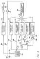
- FIGURE 4a block diagram of an adaptive predistortion linearized amplifier system employing an additive predistortion architecture is illustrated.
- the upper signal path in FIGURE 4generally corresponds to FIGURE 1A and like numerals are employed for the components described in FIGURE 1A .
- the adaptive system of FIGURE 4adds a lower feedback signal path to the system of FIGURE 1A which is coupled to the output 106 and input 104.
- the adaptive predistortion linearized amplifier systememploys a DPD controller 420 in the feedback path which employs the sampled output of the amplifier and the baseband input to generate the polynomial predistortion parameters employed in the DPD 108 (and specifically the predistortion coefficients described above in relation to the preferred embodiment of the DPD described in FIGURE 3 ). This allows the predistortion parameters to be adapted to the current operating conditions of the amplifier system to maximize effectiveness of the predistortion operation and minimize distortion.
- the baseband signal at input 104is provided to the DPD 108 in quadrature (I,Q) format along lines 400, 402 and is predistorted by the DPD 108 as described above in relation to FIGURES 1A, 1B and 3 .
- the output of DPD 108is added to the input signal provided on lines 404, 406 at addition circuits 408, 410 (comprising complex addition circuit 110 of FIGURE 1A ) to form a digital baseband predistorted signal in Cartesian (I,Q) coordinates.
- the in-phase and quadrature components of the digital baseband predistorted signalare converted into analog signals using digital-to-analog converters (DACs) 412 and 413.
- DACsdigital-to-analog converters
- the analog signalsare then quadrature modulated and up converted to RF using an analog quadrature modulator (AQM) 414 which receives a fixed frequency RF signal from local oscillator (LO) 416.
- the output of AQM 414is a predistorted modulated RF carrier.
- the predistorted carrieris used to drive the power amplifier (PA) 100.
- PApower amplifier
- the output of the amplifier on line 106is sampled by a sampling coupler 418 and the sampled analog RF signal is down converted and demodulated to an analog I,Q signal by analog quadrature demodulator (AQDM) 422.
- the up and down conversion processing of the analog signals in the systemare phase synchronized by using the same LO 416 for both down conversion and up conversion.
- the analog I,Q signal from AQDM 422is converted to I,Q digital signals by analog to digital converters 424, 426 which provide the digital sampled output I,Q signals along lines 428, 430 to DPD controller 420.
- the digital predistortion (DPD) controller 420also receives the digital baseband input signal in I,Q format along lines 432, 434.
- the DPD controller 420may be a suitably programmed DSP with associated memory.
- the DPD controller 420periodically compares the digital baseband input modulation to an estimate of the complex baseband output envelope of the amplifier to adaptively modify the values of the DPD parameters in order to ensure optimum linearity performance when changes in the operating conditions of the amplifier occur (thermal drifts, power supply fluctuations, changes in input modulation, variations in drive level, etc). These updated parameters are provided to the nonvolatile storage locations in DPD 108 as indicated by line 436.
- the DPD controller 420can also (optionally) perform spectral analyses of the output envelope estimate to optimize the linearity of the amplifier in different frequency sub-bands.
- FIGURE 5shows a block diagram of an adaptive predistortion amplifier system that employs a multiplicative predistortion architecture, in accordance with an alternate embodiment of the invention.
- the upper path of the systemcorresponds to the embodiment of FIGURE 2A and like numerals are employed for common elements.
- the adaptive operation of the systemis analogous to that described in FIGURE 4 , the main difference being that the predistorter's topology in FIGURE 5 is multiplicative rather than additive as in FIGURE 4 with the baseband I,Q input being provided along lines 500, 502 directly to DPD 202 which performs a nonlinear operation on the input signal.
- the digital predistortion (DPD) controller 520also similarly receives the digital baseband input signal in I,Q format along lines 532, 534 and the sampled output in digital form on lines 528, 530 and periodically compares the digital baseband input signal to an estimate of the complex baseband output envelope of the amplifier to adaptively modify the values of the DPD parameters. These updated parameters are provided to the storage locations in DPD 202 as indicated by line 536.
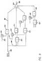
- FIGURE 6shows a flow chart diagram of a preferred embodiment of the predistortion adaptation algorithm implemented in the DPD controller in the adaptive predistortion linearized amplifier systems of FIGURE 4 or 5 .
- Estimates of the input signal to the amplifier (PA Input)are generated by a predictive DPD filter inside the DPD controller that operates on the complex baseband quadrature input (I IN , Q IN ).
- the structure and operation of the predictive DPD filterare identical to those of the DPD described in FIGURE 3 above and will not be repeated here.
- the data verifier processing block 602determines whether the samples selected by the data grabber are suitable for the computation of new predistortion parameters.
- the data synchronizer processing block 604uses fractional delay interpolation techniques to time-align the input and output data in order to compensate for amplifier and processing delays. Proper time synchronization is an important requirement for ensuring the accuracy of memory effect compensation in the DPD.
- the parameter calculator processing block 608then uses the kernel matrix and the synchronized input data PA_IN(t-delay,N) to compute the predistorter's parameters.
- the parameter calculator processing block 608preferably uses fast convergence least square processing to find an optimal set of parameter values that minimize the quadratic norm squared (average power) of the output distortion of the amplifier.
- the DPD parametersare low-pass filtered in the parameter averager processing block 608 to reduce the effects of noise and disturbances in the computation of the DPD parameters.
- the predistortion model validator processing block 612checks the consistency and validity of the parameter values computed by the parameter calculator 608 and averaged by the parameter averager 610.
- model validator 612One model validation criteria implemented in model validator 612 is to test if the magnitude of the DPD parameters is within preset bounds. If this condition is true, the parameter values are considered valid and they are provided as updated predistortion coefficients to the DPD (108 or 202).
- the predistortion model validator block 614also keeps a table of previously computed predistortion coefficients that can be used in case that the most recently computed parameters estimates are invalid or do not provide acceptable predistortion performance.
- FIGURE 7a preferred embodiment of a FIR filter which may be employed for dynamics compensation circuits 310, 314, 316, 318, and 320 described in relation to FIGURE 3 above is illustrated in a schematic drawing.
- the same basic architecture illustrated in FIGURE 7may be employed for each of the circuits with the filter coefficients varying between the specific circuits.
- the number of filter stages Nmay vary in the implementations of the individual circuits of FIGURE 3 .
- the FIR filterreceives the digital input at input 700 which will correspond to the complex input samples for the linear dynamics compensation circuit 310 and to various orders of the input envelope samples in the circuits 314, 316, 318 and 320.
- the digital input signal at 700is provided to a series of delay stages 702 equal in number to the desired filter size.
- each delay stage 702has a tap which is fed to a multiplier 704 which also receives a complex parameter (or filter coefficient) stored in nonvolatile memory 706. These individual filter coefficients are updated by the DPD controller along lines 708 in the adaptive embodiments described previously.
- the outputs of the N multipliers 704are fed to a complex addition circuit 710 which provides a complex filter output on line 712.
- FIGURE 8a preferred embodiment of a polynomial generator circuit which may be employed for the nonlinear static compensation circuit 312 of FIGURE 3 , is illustrated in a schematic drawing.
- the polynomial generator circuithas an input 800 which receives the digital envelope signal (as described above in relation to FIGURE 3 ) which is fed to a first multiplier circuit 802 which also receives a complex polynomial coefficient from nonvolatile storage 804.
- the polynomial coefficient stored in nonvolatile storage 804may be updated by the DPD controller along line 805 in an adaptive embodiment as described previously.
- the output of the multiplier 802is provided along line 806 to a complex addition circuit 810.
- the output of the multiplier 802is also provided along 808 to a second branch of the polynomial generator circuit which includes multipliers 812 and 814 and a nonvolatile storage 816 which stores a second complex polynomial coefficient. Similarly this complex polynomial coefficient may be updated as indicated by line 817 from the DPD controller.
- the output of multiplier 814is provided to addition circuit 810.
- a third branch of the polynomial generatoris provided via multiplier 818. Additional branches of the polynomial generator circuit are cascaded in a manner as illustrated in FIGURE 8 until a final branch including a final polynomial coefficient in nonvolatile storage 828 and multipliers 824 and 826 provides a final N th order complex polynomial value to addition circuit 810.
- the output of addition circuit 810is provided on line 820 and generally corresponds to the polynomial of equation (2) above.
- FIGURE 9a preferred embodiment of the autoregressive dynamics compensation circuit 322 is illustrated in a schematic drawing.
- the circuit illustratedcorresponds to an IIR filter providing both zeros and poles in the filter transfer function and accordingly corresponds generally to the implementation of equation (8) described above.
- the lower half of the circuitmay be employed with the input corresponding to the signal on line 912.
- the digital input signal at 900is provided to a series of delay stages 902 equal in number to the desired number of filter stages implemented in the numerator of equation (8).
- the output of each delay stage 902has a tap which is fed to a multiplier 904 which also receives a complex parameter (or filter coefficient) stored in nonvolatile memory 906.
- the outputs of the N multipliers 904are fed to a complex addition circuit 910 which provides a complex output on line 912.
- the output on line 912acts as an input to the all pole section of the filter.
- the signal on line 912is provided to a second series of delay stages 914 equal in number to the desired number of filter stages implemented in the denominator of equation (8), or in equation (7) in an all pole implementation of circuit 322.
- the output of each delay stage 914has a tap which is fed to a multiplier 916 which also receives a complex parameter (or filter coefficient) stored in nonvolatile memory 918.
- These individual filter coefficientsare updated by the DPD controller along lines 920 in the adaptive embodiments described previously.
- the outputs of the N multipliers 916are fed to a complex addition circuit 922 which provides a complex output to addition circuit 910 which provides an output from the filter on line 924 via line 912.
- the number of stages in the upper and lower sections of the filter, while indicated by the integer N,may in general be different.
Landscapes
- Physics & Mathematics (AREA)
- Nonlinear Science (AREA)
- Engineering & Computer Science (AREA)
- Power Engineering (AREA)
- Amplifiers (AREA)
Description
- The present invention is directed to predistortion linearization of high efficiency, high power RF amplifiers and related systems and methods.
- Modern wireless communication systems employ spectrally efficient, digitally modulated signals with wide bandwidths and time-varying envelopes. Variations in the envelope magnitude of digital modulations generate distortion components at the output of the transmitter that are caused by the inherent nonlinearity of RF amplification circuits. Amplifier distortion produces a dilation of the spectrum of the input signal ("spectral regrowth") which causes interference to communications in adjacent channels. Adjacent channel interference (ACI) is a highly undesirable phenomenon that is tightly controlled by regulatory organizations (FCC, ETSI, ITU). In addition to spectral regrowth, amplifier nonlinearities produce in-band distortion (i.e. distortion components within the bandwidth of the modulated input signal) which deteriorates the integrity of the transmitted signal and results in high Bit Error Rate (BER) at the receiver end. Nonlinearities in conventional RF amplifiers (Class AB) are relatively minor (distortion approximately 40 dB below the level of the carrier for output back offs (OBO) equal to the peak-to-average power ratio (PAR) of the modulation). The price to pay for such a mild nonlinear behavior is poor efficiency, i.e. limited DC-to-RF power conversion performance. High efficiency amplification is highly desirable since it improves system reliability (longer mean time before failure (MTBF)), simplifies thermal management, reduces amplifier size (lower silicon requirements) and lowers the operational and ownership costs of base stations. High efficiency amplifiers (e.g., Doherty amplifier designs) on the other hand exhibit much more nonlinear behavior than Class AB designs (distortion at or less than 29 dB below the level of the carrier).
- One simple method of linearization increases the level of OBO in order to reduce output distortion by extending the linear range of operation of the amplifier. This technique can be successfully applied to enhance the linearity of Class AB amplifiers. Unfortunately it also produces a severe loss in efficiency due to reductions in RF output power resulting from higher OBO levels. High efficiency amplifiers on the other hand cannot typically be linearized by simply increasing OBO and require more sophisticated linearization techniques. A well-established technique uses Cartesian (or polar) feedback to minimize the output distortion of the amplifier. Feedback linearization can be effective for narrow signal bandwidths but has very limited distortion correction capabilities when wide bandwidth operation is required (e.g. multicarrier WCDMA) due to input-output stability restrictions associated to loop dynamics. Therefore, feedback would not be sufficient to linearize wide bandwidth, highly efficient transmitters. Another technique, feed forward, is based on additive post-correction of amplifier distortion, typically employing a dual loop architecture to estimate the output distortion of the amplifier in a first (carrier cancellation) loop and then injecting the distortion estimate, properly phased and scaled, to the output of the "main" amplifier via an RF auxiliary or "error" amplifier in a second (distortion cancellation) loop. Feed forward linearization systems do not suffer from the bandwidth limitations of feedback linearizers and are unconditionally stable. However, and despite having wide bandwidth distortion correction capabilities, feed forward systems usually have low efficiency due to the DC power consumption of the error amplifier and the presence of lossy delay elements at the output of the main amplifier required for phase alignment of the distortion cancellation loop.
- An alternative technique suitable for high linearity and high efficiency amplification is predistortion linearization. Conceptually and as a first order approximation, the predistortion technique linearizes the amplifier by injecting a compensatory distortion component at the input of the amplifier whose phase is opposite (180 degrees out of phase) to that of the amplifier's output distortion and whose amplitude is that of the output distortion divided by the linear gain of the amplifier. Predistortion does not suffer from the stability and severe bandwidth restrictions of feedback linearization systems. It also has the advantage over back off and feed forward linearization that its application in a well designed system does not result in a severe degradation of amplifier efficiency. Due to these inherent advantages, predistortion linearization has been the subject of intense research over the past decade.
- Prior approaches to predistortion linearization have primarily focused on the design and implementation of digital LUT (Look Up Table) predistorters given the flexibility, precision and noise immunity advantages that they typically offer in comparison to analog predistorters. In these LUT based systems predistortion is carried out in baseband in either polar or Cartesian coordinates. In polar digital predistortion systems a conversion between Cartesian/polar coordinates is usually necessary due to the fact that the digital input modulation is in quadrature form. The coefficients of the predistorter are adaptively computed and stored in tables indexed by transformations of the input (or output) signal envelopes. Typically such LUT predistorters are intended to only compensate for nonlinear static amplifier distortion, without provisions for the linearization of dynamic nonlinearities in the amplifier. These "static" predistorters are not well suited for high efficiency base station transmitter designs due to the fact that nonlinear dynamic distortion components or "memory effects" constitute a substantial portion of the total output distortion of high power, high efficiency amplifiers.
- A method taking into account both nonlinear static and nonlinear dynamic distortions is disclosed in C. Florian et al, "CAD Identification and Validation of a non-linear Dynamic Model for Performance Analysis of Large-signal Amplifiers".
- To address this limitation of LUT predistorters nonparametric digital baseband predistorters have been proposed in which multidimensional tables are indexed by dynamic transformations (filtered versions) of the instantaneous input envelope magnitude or power. The main advantage of the multitable technique for nonlinear dynamic distortion compensation is that it does not require the computation of a parametric model of the inverse dynamics of the amplifier. The main disadvantages are large memory requirements for storing the predistortion coefficients and the computational complexity involved in the interpolation of table entries when there is unreliable/insufficient data for system adaptation. Multitable interpolation complexity can be quite substantial, posing a limit to the accuracy and adaptation rate of the predistorter. The accuracy of digital LUT predistorters is also limited by table quantization errors. Quantization errors can severely limit distortion correction in high efficiency, high power transmitters in which wideband dynamic distortion compensation is necessary to meet stringent emissions specifications. A simple way to minimize table quantization error would be to increase table size. This solution is a viable alternative for some applications employing parametric digital LUT predistorters. Unfortunately increasing the number of table entries in multitable designs is prohibitive due to the rapid increase in memory and computational requirements. To improve the accuracy and lower the complexity of LUT predistorters a number of other predistortion systems have been proposed. However, none of these approaches adequately addresses the above problems.
- The present invention is directed to overcoming the above noted shortcomings of the prior art and providing a predistortion system suitable for wide bandwidth applications without introducing undue complexity into the system.
- In a first aspect the present invention provides a digital predistorter as claimed in
claim 1. - According to another aspect the present invention provides a method for predistorting a communication signal prior to amplification by an RF amplifier as claimed in claim 10.
- Advantageous embodiments are described in the dependent claims.
- Further features and advantages of the present invention are set out in the following detailed description.
FIGURE 1A is a functional block diagram of a predistortion linearized amplifier system using an additive predistortion architecture, in accordance with a preferred embodiment of the present invention.FIGURE 1B is a functional block diagram of the predistortion signal path in the additive predistortion architecture ofFIGURE 1A , in accordance with a preferred embodiment of the present invention.FIGURE 2A is a functional block diagram of a predistortion linearized amplifier system using a multiplicative predistortion architecture, in accordance with an alternate embodiment of the present invention.FIGURE 2B is a functional block diagram of the predistortion signal path in the multiplicative predistortion architecture ofFIGURE 2A , in accordance with the alternate embodiment of the present invention.FIGURE 3 is a block diagram of a polynomial digital predistorter, in accordance with a preferred embodiment of the present invention.FIGURE 4 is a block diagram of an adaptive predistortion linearized amplifier system employing an additive predistortion architecture, in accordance with a preferred embodiment of the present invention.FIGURE 5 is a block diagram of an adaptive predistortion linearized amplifier system employing a multiplicative predistortion architecture, in accordance with an alternate embodiment of the present invention.FIGURE 6 is a flow diagram of a predistortion adaptation algorithm, in accordance with a preferred embodiment of the present invention.FIGURE 7 is a schematic diagram of a FIR filter employed in the linear and nonlinear dynamics compensation blocks of the digital predistorter ofFigure 3 , in accordance with a preferred embodiment of the present invention.FIGURE 8 is a schematic diagram of a polynomial generator circuit employed in the nonlinear static compensation block of the digital predistorter ofFigure 3 , in accordance with a preferred embodiment of the present invention.FIGURE 9 is a schematic diagram of an IIR filter employed in the autoregressive dynamics compensation block of the digital predistorter ofFigure 3 , in accordance with a preferred embodiment of the present invention.- The present invention provides a digital predistortion system and method with enhanced distortion correction capabilities. The present invention further provides an improved predistortion linearized amplifier system and related method.
FIGURES 1A and 1B show an additive predistortion system and predistortion linearized amplifier in accordance with a first embodiment of the present invention in which the distortion compensation signal is added (injected) digitally to the baseband modulation input to form the predistorted signal to drive the amplifier.FIGURES 2A and 2B show a multiplicative predistortion system and predistortion linearized amplifier in accordance with a second embodiment of the present invention in which the digital predistorter acts as a nonlinear operator in cascade with the amplifier. - Referring first to
FIGURE 1A , the predistortion linearized amplifier system in accordance with a first embodiment of the present invention includes anamplifier 100 which is preferably a high power RF amplifier of a type adapted for wireless communications applications such as cellular base stations.Amplifier 100 may advantageously be designed to have relatively high efficiency. For example, a high efficiency amplifier design employing dynamic load modulation is disclosed inUS patent application serial no. 10/837,838, filed May 3, 2004 amplifier 100 may correspond to a conventional design operated at a lower output back off level for high efficiency. Other designs foramplifier 100 may also be employed. Such efficient amplifier designs may introduce distortion into the amplified signal, however, especially for signal peaks. Adigital predistortion system 102 compensates for distortion introduced byamplifier 100 by predistorting an input signal applied to input 104. In particular,input 104 may receive a digital communication signal in the form of a complex quadrature (I,Q) signal comprising a stream of signal samples which may be modulated in any of a variety of modulation schemes well known in the art. For example, the input signal may be a wideband signal such as a WCDMA multi-carrier communication signal. In the additive architecture ofFIGURE 1A , the digital predistortion system comprises afirst signal path 120 coupled to theinput 104 and a second signal path comprising adigital predistorter 108 coupled to input 104 vialine 122 which operates on the input signal and provides a predistortion signal online 124. Anaddition circuit 110 is coupled to the first and second signal paths and injects the predistortion signal into the input signal and outputs a predistorted input signal online 126. The signal fromaddition circuit 110 is a baseband predistorted digital signal. Conventional digital to analog conversion circuitry and up conversion circuitry (shown inFIGURE 4 and discussed below) convert the predistorted digital signal to a predistorted analog RF signal. Theamplifier 100 receives and amplifies the predistorted analog RF signal and provides an amplified RF output signal online 106 which is substantially free of distortion. - In
FIGURE 1B the basic architecture of thedigital predistortion system 102 is shown. In the illustrated additive architecture the basic predistortion operation on the input signal is performed in the second signal path bydigital predistorter 108. Thepredistorter 108 preferably uses a polynomial model to accurately predistort the amplifier. More specifically, the predistorter preferably uses a discrete-time polynomial kernel to model the inverse transfer characteristic of the amplifier. Accurate predistortion is achieved by providing separate and simultaneous polynomial modeling and compensation for linear dynamic, nonlinear static, and nonlinear dynamic distortion as depicted in the functional diagram ofFIGURE 1 B byblocks dynamic block 112 compensates for in-band distortion due to the amplifier 100 (and also in-band distortion due to other active components, including analog quadrature modulation errors, due to the AQM circuitry shown inFIGURE 4 ). The nonlinearstatic block 114 of the predistorter compensates for distortion due to instantaneous input signal levels, so called memoryless distortion. The nonlineardynamic block 116 of the predistorter compensates for dynamic distortion which is a function of plural consecutive input signal levels, so called memory effects. This nonlinear dynamic distortion has two general types of contributions having quite different characteristics which can be generally described as short term memory effects which are primarily reactive electrical effects and long term memory effects including thermal memory effects. To effectively model and compensate for these two types of memory effects the nonlineardynamic block 116 of the predistorter preferably employs separate polynomial models for the two types of memory effects. These are preferably cascaded for computational efficiency and reduced circuit complexity within nonlineardynamic block 116 as will be discussed in detail below. The compensatory predistortion signal components emerging from the linear dynamic, nonlinear static, and nonlinear dynamic blocks of the predistorter are summed together atcombiner 118 to form a unique distortion compensation signal online 124. This predistortion signal is then added to the input signal ataddition circuit 110 as described above. One specific implementation of thedigital predistorter 108 is shown inFIGURE 3 , discussed below. - Referring to
FIGURES 2A and 2B a second embodiment of the present invention is illustrated in which the digital predistorter acts as a nonlinear operator in cascade with the input and the amplifier and performs a multiplicative predistortion operation on the input signal. As in the first embodiment of the present invention the predistortion linearized amplifier system includes an amplifier 200 (which may be the same asamplifier 100 and is not described further) which is linearized bydigital predistorter 202 acting on a digital input signal provided atinput 204. The input signal is provided on line 216 (complex I,Q signal inputs and signal paths are implied) and operated on by a multiplicative predistortion operation to provide a pedistorted input signal online 218. Digital to analog and up conversion circuits (not shown inFIGURE 2A but described in relation toFIGURE 5 below) convert the predistorted input signal to an RF signal which is amplified byamplifier 200 to provide a substantially distortion free output RF signal online 206. InFIGURE 2B the architecture of thedigital predistorter 202 is illustrated. As in the case ofdigital predistorter 108 of the first embodiment thedigital predistorter 202 provides separate and simultaneous polynomial modeling and compensation for linear dynamic, nonlinear static, and nonlinear dynamic distortion as depicted in the functional diagram ofFIGURE 2B byblocks combiner 214 to provide the predistorted input signal online 218. Due to the flexibility of the multiple polynomial modeling of the predistortion operation the same architecture may be used for the multiplicative embodiment as the additive embodiment ofFIGURE 1A and 1B and one specific implementation of thedigital predistorter 202 is shown inFIGURE 3 , discussed below. - Referring to
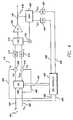
FIGURE 3 the structure of the digital predistorter (DPD) in accordance with a preferred embodiment of this invention is shown in a block schematic drawing. The input to the digital polynomial predistorter (DPD IN) is provided atinput 300. As discussed above this will correspond to a baseband communication signal comprising a stream of signal samples in quadrature (I,Q) format. The stream of input signal samples are provided alongsignal path 304 to lineardynamics compensation circuit 310. The lineardynamic compensation circuit 310 provides a linear operation on a plurality of time delayed signal samples to model linear dynamic distortion or linear memory effects. More specifically, the linear dynamic operation may be represented by the following polynomial operation:
- In equation (1) H1[Z] is the transfer function of the linear
dynamics compensation circuit 310, a0 - aN1 are complex predistortion coefficients and N1 is an integer which determines the number of delayed samples employed to model the memory effects. This polynomial operation is preferably implemented in a digital Finite Impulse Response (FIR) filter and the complex predistortion coefficients are filter coefficients stored in nonvolatile memory within lineardynamics compensation circuit 310. - The stream of input signal samples at
DPD input 300 are also provided to nonlinear static and nonlinear dynamics compensation blocks. These generate nonlinear predistortion component signals by performing nonlinear transformations of the magnitude of the envelope of the input signal. More specifically, adigital envelope detector 324 receives the input samples alongline 308 and computes envelope samples corresponding to the instantaneous envelope of the input signal. The output envelope samples from thedigital envelope detector 324 are provided alongline 326 to nonlinearstatic compensation circuit 312. Nonlinearstatic compensation circuit 312 provides a nonlinear static polynomial transformation on individual envelope samples output from the digital envelope detector to model nonlinear static (memoryless) distortion. More specifically, the nonlinear operation may be represented by the following polynomial operation:
- In equation (2) H2 is the transfer function of the nonlinear
static compensation circuit 312, the pk are complex predistortion coefficients, DPDINenv represents the current envelope sample from thedigital envelope detector 324, and M is an integer. - The output envelope samples from the
digital envelope detector 324 are also provided to a nonlinear dynamics compensation block which provides a nonlinear operation on a plurality of delayed envelope signal samples to generate a distortion compensation signal in response to variations in envelope magnitude dynamics. The nonlinear dynamics compensation block preferably comprises first and second dynamics compensation circuits in a cascade configuration. The first nonlinear dynamic compensation circuit preferably comprises a bank of parallelpolynomial operation circuits - Specifically, in a preferred implementation envelope
dynamics compensation circuit 314 implements the following polynomial operation on plural delayed envelope samples provided on line 328:
- In equation (3) H3[z] is the transfer function of the envelope
dynamics compensation circuit 314, b1 - bN2 are complex predistortion coefficients and N2 is an integer which determines the number of delayed samples employed to model the memory effects. This polynomial operation is preferably implemented in a digital Finite Impulse Response (FIR) filter and the complex predistortion coefficients are filter coefficients stored in nonvolatile memory within envelopedynamics compensation circuit 314. As shown inFIGURE 3 additional higher order memory effect compensation is also provided in parallel with the envelopedynamics compensation circuit 314 by acting on higher order multiples of the envelope samples. In particular, 3rd orderdynamics compensation circuit 316 operates on a second order envelope sample provided bymultiplier 336 and implements the following polynomial operation on plural delayed envelope samples provided on line 332:
- In equation (4) H4[z] is the transfer function of the 3rd order
dynamics compensation circuit 316, C1 -CN3 are complex predistortion coefficients and N3 is an integer which determines the number of delayed samples employed to model the third order memory effects. This polynomial operation is preferably implemented in a digital Finite Impulse Response (FIR) filter and the complex predistortion coefficients are filter coefficients stored in nonvolatile memory within 3rd orderdynamics compensation circuit 316. Similarly, 4rth orderdynamics compensation circuit 318 operates on third order envelope samples provided bymultiplier 338 and implements the following polynomial operation on plural delayed envelope samples provided on line 334:
and 5th orderdynamics compensation circuit 320 operates on fourth order envelope samples provided bymultiplier 336 and implements the following polynomial operation on plural delayed envelope samples provided on line 346:
- In equations (5) and (6) H5[z] and H6[z] are the transfer functions of
circuits dynamics compensation circuits - Still referring to
FIGURE 3 , second nonlineardynamics compensation circuit 322 is cascaded with the first nonlinear dynamics compensation circuit and implements an autoregressive dynamics compensation operation. The autoregressive dynamics compensation operation cancels the distortion due to thermal drifts and long-term dynamics in the amplifier. To reduce circuit complexity the second nonlineardynamics compensation circuit 322 is preferably coupled in a cascade arrangement with the combined outputs of the plural parallel dynamicmemory compensation circuits static compensation circuit 312. The outputs of these circuits are summed together atcombiner 342 and the output ofcombiner 342 is provided to the second nonlineardynamics compensation circuit 322 which implements the autoregressive dynamics compensation operation using an infinite impulse response (IIR) digital filter. Specifically, the following operation may be implemented using an all pole IIR filter:
- More generally, the following operation may be implemented in
circuit 322 using an IIR filter:
- In equations (7) and (8), H7[z] and H8[z] are the transfer function of
circuit 322, bN and gN are complex filter coefficients and N6, N7 and N8 are integers. - The output of the autoregressive
dynamics compensation circuit 322 is used to modulate the I,Q baseband input signal provided online 306 atmultiplier 344. This modulated signal is added to the output of the lineardynamics compensation circuit 310 ataddition circuit 348 to form the DPD output which is provided online 302. - The polynomial
digital predistortion circuits FIGURES 7-9 , described below. The other circuit components inFIGURE 3 are conventional digital circuit components and also may be readily implemented in FPGA/ASIC technology, as will be appreciated by those skilled in the art. - The specific implementation shown in
FIGURE 3 may be modified to accommodate the specific application and relevant cost and complexity constraints. For example, althoughFIGURE 3 depicts a predistorter that provides up to 5th order reactive memory effect compensation only, higher order compensation can be readily implemented by adding additional dynamic memory compensation branches and are also implied herein. Also, in some implementations it may be desirable to have only odd order memory effect compensation, for example to reduce circuit complexity or provide higher than 5th odd order correction without additional circuits, and such an embodiment is also implied herein. Also, the manner in which the circuits are cascaded may be varied while retaining the flexible polynomial modeling of the distortion compensation. Additional variations and modifications are also possible as will be appreciated by those skilled in the art. - Referring to
FIGURE 4 a block diagram of an adaptive predistortion linearized amplifier system employing an additive predistortion architecture is illustrated. The upper signal path inFIGURE 4 generally corresponds toFIGURE 1A and like numerals are employed for the components described inFIGURE 1A . The adaptive system ofFIGURE 4 adds a lower feedback signal path to the system ofFIGURE 1A which is coupled to theoutput 106 andinput 104. The adaptive predistortion linearized amplifier system employs aDPD controller 420 in the feedback path which employs the sampled output of the amplifier and the baseband input to generate the polynomial predistortion parameters employed in the DPD 108 (and specifically the predistortion coefficients described above in relation to the preferred embodiment of the DPD described inFIGURE 3 ). This allows the predistortion parameters to be adapted to the current operating conditions of the amplifier system to maximize effectiveness of the predistortion operation and minimize distortion. - More specifically, as shown in
FIGURE 4 the baseband signal atinput 104 is provided to theDPD 108 in quadrature (I,Q) format alonglines DPD 108 as described above in relation toFIGURES 1A, 1B and3 . The output ofDPD 108 is added to the input signal provided onlines addition circuits 408, 410 (comprisingcomplex addition circuit 110 ofFIGURE 1A ) to form a digital baseband predistorted signal in Cartesian (I,Q) coordinates. The in-phase and quadrature components of the digital baseband predistorted signal are converted into analog signals using digital-to-analog converters (DACs) 412 and 413. The analog signals are then quadrature modulated and up converted to RF using an analog quadrature modulator (AQM) 414 which receives a fixed frequency RF signal from local oscillator (LO) 416. The output ofAQM 414 is a predistorted modulated RF carrier. As discussed previously the analog quadrature modulation operation can introduce in-band distortion which is also compensated byDPD 108. The predistorted carrier is used to drive the power amplifier (PA) 100. The output of the amplifier online 106 is sampled by asampling coupler 418 and the sampled analog RF signal is down converted and demodulated to an analog I,Q signal by analog quadrature demodulator (AQDM) 422. The up and down conversion processing of the analog signals in the system are phase synchronized by using thesame LO 416 for both down conversion and up conversion. The analog I,Q signal fromAQDM 422 is converted to I,Q digital signals by analog todigital converters lines DPD controller 420. The digital predistortion (DPD)controller 420 also receives the digital baseband input signal in I,Q format alonglines DPD controller 420 may be a suitably programmed DSP with associated memory. TheDPD controller 420 periodically compares the digital baseband input modulation to an estimate of the complex baseband output envelope of the amplifier to adaptively modify the values of the DPD parameters in order to ensure optimum linearity performance when changes in the operating conditions of the amplifier occur (thermal drifts, power supply fluctuations, changes in input modulation, variations in drive level, etc). These updated parameters are provided to the nonvolatile storage locations inDPD 108 as indicated byline 436. TheDPD controller 420 can also (optionally) perform spectral analyses of the output envelope estimate to optimize the linearity of the amplifier in different frequency sub-bands. FIGURE 5 shows a block diagram of an adaptive predistortion amplifier system that employs a multiplicative predistortion architecture, in accordance with an alternate embodiment of the invention. The upper path of the system corresponds to the embodiment ofFIGURE 2A and like numerals are employed for common elements. The adaptive operation of the system is analogous to that described inFIGURE 4 , the main difference being that the predistorter's topology inFIGURE 5 is multiplicative rather than additive as inFIGURE 4 with the baseband I,Q input being provided alonglines DPD 202 which performs a nonlinear operation on the input signal. The operation ofDACs AQM 514,LO 516,sampling coupler 518,AQDM 522,ADCs FIGURE 4 and need not be described further. The digital predistortion (DPD)controller 520 also similarly receives the digital baseband input signal in I,Q format alonglines lines DPD 202 as indicated byline 536.- Although the specific parameter values will differ between the embodiments of
FIGURE 4 andFIGURE 5 , due to the flexibility of the polynomial model described in relation toFIGURE 3 the same architecture forDPD DPD controllers FIGURE 6 shows a flow chart diagram of a preferred embodiment of the predistortion adaptation algorithm implemented in the DPD controller in the adaptive predistortion linearized amplifier systems ofFIGURE 4 or5 . Estimates of the input signal to the amplifier (PA Input) are generated by a predictive DPD filter inside the DPD controller that operates on the complex baseband quadrature input (IIN, QIN). The structure and operation of the predictive DPD filter are identical to those of the DPD described inFIGURE 3 above and will not be repeated here. The predicted PA Input signal and the downconverted/digitized complex baseband signal estimate of the output envelope of the amplifier (PA Output) are processed by the datagrabber processing block 600 which selects N samples from the estimated PA Input and the PA Output to form the data buffers to be used for DPD adaptation:

- The data
verifier processing block 602 then determines whether the samples selected by the data grabber are suitable for the computation of new predistortion parameters. One verification criteria implemented in thedata verifier block 602 is to test if the crest factor (CF) of the grabbed PA Input data exceeds a preset threshold CFthres:
- If this condition is true, the data is verified as good then it is presented to the data
synchronizer processing block 604 which uses fractional delay interpolation techniques to time-align the input and output data in order to compensate for amplifier and processing delays. Proper time synchronization is an important requirement for ensuring the accuracy of memory effect compensation in the DPD. The time-aligned input (PA_IN(t-delay,N)) and output (PA_OUT(t-delay,N)) data buffers are then processed by the predistortion model builder processing block 606 which uses the synchronized data to compute a kernel matrix K that implements in software the DPD structure shown inFIGURE 3 :
- The parameter
calculator processing block 608 then uses the kernel matrix and the synchronized input data PA_IN(t-delay,N) to compute the predistorter's parameters. The parametercalculator processing block 608 preferably uses fast convergence least square processing to find an optimal set of parameter values that minimize the quadratic norm squared (average power) of the output distortion of the amplifier. The DPD parameters are low-pass filtered in the parameteraverager processing block 608 to reduce the effects of noise and disturbances in the computation of the DPD parameters. Finally the predistortion modelvalidator processing block 612 checks the consistency and validity of the parameter values computed by theparameter calculator 608 and averaged by theparameter averager 610. One model validation criteria implemented inmodel validator 612 is to test if the magnitude of the DPD parameters is within preset bounds. If this condition is true, the parameter values are considered valid and they are provided as updated predistortion coefficients to the DPD (108 or 202). The predistortionmodel validator block 614 also keeps a table of previously computed predistortion coefficients that can be used in case that the most recently computed parameters estimates are invalid or do not provide acceptable predistortion performance. - Referring to
FIGURE 7 a preferred embodiment of a FIR filter which may be employed fordynamics compensation circuits FIGURE 3 above is illustrated in a schematic drawing. The same basic architecture illustrated inFIGURE 7 may be employed for each of the circuits with the filter coefficients varying between the specific circuits. Also, the number of filter stages N may vary in the implementations of the individual circuits ofFIGURE 3 . As shown, the FIR filter receives the digital input atinput 700 which will correspond to the complex input samples for the lineardynamics compensation circuit 310 and to various orders of the input envelope samples in thecircuits delay stage 702 has a tap which is fed to amultiplier 704 which also receives a complex parameter (or filter coefficient) stored innonvolatile memory 706. These individual filter coefficients are updated by the DPD controller alonglines 708 in the adaptive embodiments described previously. The outputs of theN multipliers 704 are fed to acomplex addition circuit 710 which provides a complex filter output online 712. - Referring to
FIGURE 8 a preferred embodiment of a polynomial generator circuit which may be employed for the nonlinearstatic compensation circuit 312 ofFIGURE 3 , is illustrated in a schematic drawing. As shown the polynomial generator circuit has aninput 800 which receives the digital envelope signal (as described above in relation toFIGURE 3 ) which is fed to afirst multiplier circuit 802 which also receives a complex polynomial coefficient fromnonvolatile storage 804. The polynomial coefficient stored innonvolatile storage 804 may be updated by the DPD controller alongline 805 in an adaptive embodiment as described previously. The output of themultiplier 802 is provided alongline 806 to acomplex addition circuit 810. The output of themultiplier 802 is also provided along 808 to a second branch of the polynomial generator circuit which includesmultipliers nonvolatile storage 816 which stores a second complex polynomial coefficient. Similarly this complex polynomial coefficient may be updated as indicated byline 817 from the DPD controller. The output ofmultiplier 814 is provided toaddition circuit 810. A third branch of the polynomial generator is provided viamultiplier 818. Additional branches of the polynomial generator circuit are cascaded in a manner as illustrated inFIGURE 8 until a final branch including a final polynomial coefficient innonvolatile storage 828 andmultipliers addition circuit 810. The output ofaddition circuit 810 is provided online 820 and generally corresponds to the polynomial of equation (2) above. - Referring to
FIGURE 9 a preferred embodiment of the autoregressivedynamics compensation circuit 322 is illustrated in a schematic drawing. The circuit illustrated corresponds to an IIR filter providing both zeros and poles in the filter transfer function and accordingly corresponds generally to the implementation of equation (8) described above. In an all pole implementation corresponding to equation (7) the lower half of the circuit may be employed with the input corresponding to the signal online 912. The digital input signal at 900 is provided to a series of delay stages 902 equal in number to the desired number of filter stages implemented in the numerator of equation (8). The output of eachdelay stage 902 has a tap which is fed to amultiplier 904 which also receives a complex parameter (or filter coefficient) stored innonvolatile memory 906. These individual filter coefficients are updated by the DPD controller alonglines 908 in the adaptive embodiments described previously. The outputs of theN multipliers 904 are fed to acomplex addition circuit 910 which provides a complex output online 912. The output online 912 acts as an input to the all pole section of the filter. The signal online 912 is provided to a second series of delay stages 914 equal in number to the desired number of filter stages implemented in the denominator of equation (8), or in equation (7) in an all pole implementation ofcircuit 322. The output of eachdelay stage 914 has a tap which is fed to amultiplier 916 which also receives a complex parameter (or filter coefficient) stored innonvolatile memory 918. These individual filter coefficients are updated by the DPD controller along lines 920 in the adaptive embodiments described previously. The outputs of theN multipliers 916 are fed to acomplex addition circuit 922 which provides a complex output toaddition circuit 910 which provides an output from the filter online 924 vialine 912. The number of stages in the upper and lower sections of the filter, while indicated by the integer N, may in general be different. - The present invention has been described in relation to a presently preferred embodiment, however, it will be appreciated by those skilled in the art that a variety of modifications, too numerous to describe, may be made while remaining within the scope of the present invention. Accordingly, the above detailed description should be viewed as illustrative only and not limiting in nature.


Claims (12)
- A digital predistorter, comprising:- an input (300) arranged for receiving a digital communication signal comprising a stream of signal samples;- a linear dynamic compensation circuit (310) coupled to the input (300) and arranged for providing a linear operation on a plurality of time delayed input signal samples;- a digital envelope detector (324) coupled to the input (300) and arranged for providing a stream of discrete digital envelope signal samples corresponding to the input signal samples;- a nonlinear static compensation circuit (312) coupled (326) to said detector (324) output and arranged for providing a nonlinear static polynomial transformation on individual envelope signal samples output;- a first nonlinear dynamic compensation circuit including a bank of parallel polynomial circuits (314, 316, 318, 320) coupled to the envelope detector (324) and arranged for providing a nonlinear operation on a plurality of delayed envelope signal samples;- a combiner (342) arranged for combining output from said nonlinear static compensation circuit (312) and said first nonlinear dynamic compensation circuit (314, 316, 318, 320);- a second nonlinear dynamics compensation circuit (322) coupled to an output of the combiner (342) and arranged for providing an autoregressive operation on plural samples of the output of the combiner (342);- a multiplier (344) arranged for modulating the digital communication signal with an output of the second nonlinear dynamics compensation circuit (322); and- an addition circuit (348) arranged for combining the outputs of the linear dynamics compensation circuit (310) and the multiplier (344), and for providing a digital predistortion signal as an output (302).
- A digital predistorter as set out in claim 1, wherein said nonlinear static compensation circuit (312) is coupled to the envelope detector (324) in parallel with the first nonlinear dynamics compensation circuit (314, 316, 318, 320) and providing a nonlinear operation on individual digital envelope signal samples.
- A digital predistorter as set out in claim 1, wherein said linear dynamics compensation circuit (310) comprises a finite impulse response filter.
- A digital predistorter as set out in claim 1, wherein the bank of parallel polynomial circuits (314, 316, 318, 320) comprises a plurality of finite impulse response filters coupled in a parallel configuration.
- A digital predistorter as set out in claim 4, further comprising a plurality of multipliers (336, 338, 340) coupled to said envelope detector (324) and wherein said plurality of finite impulse response filters (316, 318, 320) are coupled to respective multiplier outputs (332, 334, 346) and are arranged to operate on plural higher order envelope samples.
- A digital predistorter as set out in claim 5, wherein said plural finite impulse response filters (314, 316, 318, 320) respectively are arranged to operate on at least second, third, fourth and fifth order envelope samples.
- A digital predistorter as set out in claim 1, wherein said second nonlinear dynamics compensation circuit (322) comprises an infinite impulse response filter.
- A digital predistorter as set out in claim 2, wherein said nonlinear static compensation circuit (312) comprises a polynomial generator providing a weighted polynomial from each individual envelope sample.
- A digital predistorter as set out in claim 8, wherein said polynomial generator comprises a plurality of multipliers (802, 812, 814, 818) arranged for receiving said individual envelope samples and for creating higher order envelope samples, a plurality of circuits providing complex coefficients to said multipliers (802, 812, 814, 818) and a summing circuit (810) for combining the plural weighted higher order envelope samples.
- A method for adaptive predistortion linearization of an RF amplifier system, comprising :- receiving at an input (300) a digital communication signal comprising a stream of signal samples;- operating on said input signal samples with a plurality of separate polynomial based operations and providing a stream of predistorted input samples, said polynomial based operations comprising:a first finite impulse response filtering operation of a linear dynamic compensation circuit (310) coupled to the input (300), employing a first set of adaptive complex coefficients and providing a linear operation on a plurality of time delayed input signal samples;a digital envelope detection of a digital envelope detector (324) coupled to the input (300), providing a stream of discrete digital envelope signal samples corresponding to the input signal samples;a nonlinear static polynomial transformation on individual envelope samples output by a nonlinear static compensation circuit (312);a second finite impulse response filtering operation of a first nonlinear dynamic compensation circuit including a bank of parallel polynomial circuits (314, 316, 318, 320) coupled to the envelope detector (324), employing a second set of adaptive complex coefficients and providing a nonlinear operation on a plurality of delayed envelope signal samples;a combination by a combiner (342) of an output from said nonlinear static compensation circuit (312) and said first nonlinear dynamics compensation circuit (314, 316, 318, 320);an infinite impulse response filtering operation of a second nonlinear dynamics compensation circuit (322) coupled to an output of the combiner (342), employing a third set of adaptive complex coefficients and providing an autoregressive operation on plural samples of the output of the combiner (342);a modulation by a multiplier (344) for modulating the digital communication signal with an output of the second nonlinear dynamics compensation circuit (322); anda combination by an addition circuit (348) for combining the outputs of the linear dynamics compensation circuit (310) and the multiplier (344), and for providing a digital predistortion signal as an output (302);- providing an analog predistorted RF input signal from the predistorted input samples;- amplifying said analog predistorted RF input signal to provide an output signal;- sampling the amplifier output signal and providing an analog sampled output signal;- converting said analog sampled output signal to a digital sampled output signal; and- generating updated adaptive complex coefficients employing the digital sampled output signal and the input signal samples and employing the updated coefficients for said polynomial based predistortion operations.
- A method for adaptive predistortion linearization of an RF amplifier system, as set out in claim 10, wherein providing a non-linear operation on a plurality of delayed envelope signal samples comprises operating on said plurality of delayed envelope signal samples with with a plurality of parallel polynomial operations.
- A method for adaptive predistortion linearization of an RF amplifier system as set out in claim 10, wherein said second finite impulse response filtering operation and said infinite impulse response filtering operation are performed in series.
Priority Applications (1)
| Application Number | Priority Date | Filing Date | Title |
|---|---|---|---|
| EP12178651AEP2521261A1 (en) | 2004-01-21 | 2005-01-18 | Wideband enhanced digital injection predistortion system and method |
Applications Claiming Priority (3)
| Application Number | Priority Date | Filing Date | Title |
|---|---|---|---|
| US53793704P | 2004-01-21 | 2004-01-21 | |
| US11/036,805US7366252B2 (en) | 2004-01-21 | 2005-01-14 | Wideband enhanced digital injection predistortion system and method |
| PCT/US2005/001449WO2005069897A2 (en) | 2004-01-21 | 2005-01-18 | Wideband enhanced digital injection predistortion system and method |
Related Child Applications (1)
| Application Number | Title | Priority Date | Filing Date |
|---|---|---|---|
| EP12178651.1Division-Into | 2012-07-31 |
Publications (3)
| Publication Number | Publication Date |
|---|---|
| EP1738511A2 EP1738511A2 (en) | 2007-01-03 |
| EP1738511A4 EP1738511A4 (en) | 2010-05-26 |
| EP1738511B1true EP1738511B1 (en) | 2012-10-31 |
Family
ID=34752547
Family Applications (2)
| Application Number | Title | Priority Date | Filing Date |
|---|---|---|---|
| EP12178651AWithdrawnEP2521261A1 (en) | 2004-01-21 | 2005-01-18 | Wideband enhanced digital injection predistortion system and method |
| EP05722448AExpired - LifetimeEP1738511B1 (en) | 2004-01-21 | 2005-01-18 | Wideband enhanced digital injection predistortion system and method |
Family Applications Before (1)
| Application Number | Title | Priority Date | Filing Date |
|---|---|---|---|
| EP12178651AWithdrawnEP2521261A1 (en) | 2004-01-21 | 2005-01-18 | Wideband enhanced digital injection predistortion system and method |
Country Status (5)
| Country | Link |
|---|---|
| US (1) | US7366252B2 (en) |
| EP (2) | EP2521261A1 (en) |
| KR (1) | KR100789125B1 (en) |
| CN (1) | CN101040502B (en) |
| WO (1) | WO2005069897A2 (en) |
Families Citing this family (89)
| Publication number | Priority date | Publication date | Assignee | Title |
|---|---|---|---|---|
| US8811917B2 (en) | 2002-05-01 | 2014-08-19 | Dali Systems Co. Ltd. | Digital hybrid mode power amplifier system |
| US8380143B2 (en) | 2002-05-01 | 2013-02-19 | Dali Systems Co. Ltd | Power amplifier time-delay invariant predistortion methods and apparatus |
| US7430248B2 (en)* | 2004-01-27 | 2008-09-30 | Crestcom, Inc. | Predistortion circuit and method for compensating nonlinear distortion in a digital RF communications transmitter |
| JP4976648B2 (en)* | 2004-10-27 | 2012-07-18 | 株式会社エヌ・ティ・ティ・ドコモ | Predistorter |
| US7365605B1 (en)* | 2005-01-05 | 2008-04-29 | Hoover D Robert | High voltage, high current, and high accuracy amplifier |
| US8224265B1 (en)* | 2005-06-13 | 2012-07-17 | Rf Micro Devices, Inc. | Method for optimizing AM/AM and AM/PM predistortion in a mobile terminal |
| US7831221B2 (en)* | 2005-12-13 | 2010-11-09 | Andrew Llc | Predistortion system and amplifier for addressing group delay modulation |
| US20080111622A1 (en)* | 2006-11-14 | 2008-05-15 | Roland Sperlich | Hybrid Doherty Amplifier System and Method |
| US7729420B1 (en)* | 2006-11-24 | 2010-06-01 | Kiomars Anvari | Reconditioning equalizer filter for OFDM and non-OFDM signals |
| US8619847B1 (en)* | 2006-11-24 | 2013-12-31 | Altera Corporation | Reconditioning equalizer filter for non-constant envelop signals |
| US8078561B2 (en)* | 2006-12-01 | 2011-12-13 | Uti Limited Partnership | Nonlinear behavior models and methods for use thereof in wireless radio systems |
| US7729446B2 (en)* | 2006-12-01 | 2010-06-01 | Texas Instruments Incorporated | System and method for digitally correcting a non-linear element using a multiply partitioned architecture for predistortion |
| US7822146B2 (en)* | 2006-12-01 | 2010-10-26 | Texas Instruments Incorporated | System and method for digitally correcting a non-linear element |
| CN102017553B (en) | 2006-12-26 | 2014-10-15 | 大力系统有限公司 | Method and system for baseband predistortion linearization in a multi-channel broadband communication system |
| US8131218B2 (en)* | 2007-04-13 | 2012-03-06 | General Dynamics C4 Systems, Inc. | Methods and apparatus for wirelessly communicating signals that include embedded synchronization/pilot sequences |
| EP2001127B1 (en) | 2007-06-08 | 2012-01-11 | SIAE Microelettronica S.p.A. | System and method for linearizing microwave transmitters |
| US8463374B2 (en)* | 2007-06-28 | 2013-06-11 | University Of Virginia Patent Foundation | Method, system and computer program product for controlling complex rhythmic systems |
| US7899416B2 (en)* | 2007-11-14 | 2011-03-01 | Crestcom, Inc. | RF transmitter with heat compensation and method therefor |
| KR101109861B1 (en)* | 2008-01-15 | 2012-02-14 | 미쓰비시덴키 가부시키가이샤 | Predistorter |
| US8064851B2 (en)* | 2008-03-06 | 2011-11-22 | Crestcom, Inc. | RF transmitter with bias-signal-induced distortion compensation and method therefor |
| CN101247153B (en)* | 2008-03-13 | 2011-11-30 | 中兴通讯股份有限公司 | Method for improving power amplifier efficiency and digital predistortion broadband communicator |
| US8379752B2 (en)* | 2008-03-19 | 2013-02-19 | General Dynamics C4 Systems, Inc. | Methods and apparatus for multiple-antenna communication of wireless signals with embedded synchronization/pilot sequences |
| US8331420B2 (en)* | 2008-04-14 | 2012-12-11 | General Dynamics C4 Systems, Inc. | Methods and apparatus for multiple-antenna communication of wireless signals with embedded pilot signals |
| US8090051B2 (en)* | 2008-04-29 | 2012-01-03 | Motorola Solutions, Inc. | Combined feedback and feed-forward linearization of radio frequency (RF) power amplifiers |
| CN101286963B (en)* | 2008-05-30 | 2010-09-08 | 北京北方烽火科技有限公司 | Wideband adaptive digital predistortion engine apparatus based on programmable device |
| US8331879B2 (en)* | 2008-10-15 | 2012-12-11 | Research In Motion Limited | Multi-dimensional Volterra series transmitter linearization |
| KR101616873B1 (en)* | 2008-12-23 | 2016-05-02 | 삼성전자주식회사 | apparatus and method for estimating power requirement of digital amplifier |
| WO2010073803A1 (en)* | 2008-12-27 | 2010-07-01 | 住友電気工業株式会社 | Distortion compensating circuit and radio base station |
| US8170508B2 (en) | 2009-05-07 | 2012-05-01 | Rockstar Bidco Lp | Pre-distortion for a radio frequency power amplifier |
| US8744009B2 (en)* | 2009-09-25 | 2014-06-03 | General Dynamics C4 Systems, Inc. | Reducing transmitter-to-receiver non-linear distortion at a transmitter prior to estimating and cancelling known non-linear distortion at a receiver |
| US8355466B2 (en)* | 2009-09-25 | 2013-01-15 | General Dynamics C4 Systems, Inc. | Cancelling non-linear power amplifier induced distortion from a received signal by moving incorrectly estimated constellation points |
| US8446979B1 (en) | 2010-03-02 | 2013-05-21 | Pmc-Sierra, Inc. | Predistortion with integral crest-factor reduction and reduced observation bandwidth |
| KR20110103628A (en)* | 2010-03-15 | 2011-09-21 | 삼성전자주식회사 | Digital Predistortion Apparatus and Method for Improving Performance Using Peak Level Expansion |
| CN101841304B (en)* | 2010-04-02 | 2012-02-29 | 北京交通大学 | Power amplifier with linearity corrector |
| EP2378669B1 (en)* | 2010-04-15 | 2013-03-27 | Research In Motion Limited | Communications device with separate I and Q phase power amplification having selective phase and magnitude adjustment and related methods |
| US8451941B2 (en) | 2010-04-15 | 2013-05-28 | Research In Motion Limited | Communications device with separate I and Q phase power amplification having selective phase and magnitude adjustment and related methods |
| KR101677294B1 (en)* | 2010-04-19 | 2016-11-18 | 삼성전자주식회사 | Smoothing apparatus for peak windowing |
| US10387592B1 (en) | 2010-05-26 | 2019-08-20 | Keysight Technologies, Inc. | Method and system for characterizing, modeling and simulating non-linear components having long term memory effects |
| CN103597807B (en) | 2010-09-14 | 2015-09-30 | 大理系统有限公司 | Remotely reconfigurable distributed antenna system and method |
| KR20120070057A (en)* | 2010-12-21 | 2012-06-29 | 한국전자통신연구원 | Predistortion apparatus and method for the same |
| CN102769589B (en)* | 2011-05-05 | 2016-01-13 | 中兴通讯股份有限公司 | A kind of method and system improving digital pre-distortion performance |
| US8478210B2 (en)* | 2011-05-10 | 2013-07-02 | Texas Instruments Incorporated | Apparatus and method of digital predistortion for power amplifiers with dynamic nonlinearities |
| GB2490749A (en)* | 2011-05-12 | 2012-11-14 | Nokia Siemens Networks Oy | Linearization of an RF power amplifier using a combined FIR-IIR amplifier model |
| JP6080854B2 (en)* | 2011-09-22 | 2017-02-15 | ダリ システムズ カンパニー リミテッド | System and method for increasing the bandwidth of digital predistortion in a multi-channel broadband communication system |
| US8914271B2 (en)* | 2011-11-30 | 2014-12-16 | Keysight Technologies, Inc. | Method for predistorting signals for non-linear components in the presence of long term memory effects |
| WO2013078655A1 (en)* | 2011-12-01 | 2013-06-06 | 华为技术有限公司 | Optical signal compensation device |
| JP5783070B2 (en)* | 2012-01-31 | 2015-09-24 | 富士通株式会社 | Signal processing system and signal processing method |
| US8798559B2 (en)* | 2012-02-28 | 2014-08-05 | Telefonaktiebolaget L M Ericsson (Publ) | FIR/IIR filter predistorter for power amplifiers exhibiting short-term and/or long-term memory effects |
| US8787494B2 (en)* | 2012-06-11 | 2014-07-22 | Telefonaktiebolaget L M Ericsson (Publ) | Modeling digital predistorter |
| US20150244329A1 (en)* | 2012-10-16 | 2015-08-27 | Nokia Solutions And Networks Oy | Technique for Extremely High Order IM Correction |
| KR101389880B1 (en)* | 2012-10-31 | 2014-05-07 | 한국과학기술원 | Apparatus and method for low cost implementation of adaptive digital predistortion algorithm using envelope detection feedback |
| US8842033B1 (en)* | 2013-09-30 | 2014-09-23 | Agilent Technologies, Inc. | Dynamic linearity corrector for digital-to-analog converters |
| KR102075402B1 (en) | 2013-10-11 | 2020-02-11 | 주식회사 쏠리드 | Broad band high linear power amplifier |
| US9007250B1 (en)* | 2013-10-22 | 2015-04-14 | L-3 Communications Corp. | Time-interleaved and sub-band reconstruction approaches to digital-to-analog conversion for high sample rate waveform generation |
| US9337781B2 (en) | 2013-12-09 | 2016-05-10 | King Fahd University Of Petroleum And Minerals | Augmented twin nonlinear two-box modeling and predistortion method for power amplifiers and transmitters |
| US9306606B2 (en)* | 2014-06-10 | 2016-04-05 | The Boeing Company | Nonlinear filtering using polyphase filter banks |
| US10033568B2 (en) | 2014-07-04 | 2018-07-24 | Ses S.A. | Methods, devices, and computer programs for compensating nonlinearities of a communication channel |
| CN105445682B (en)* | 2014-07-25 | 2018-08-21 | 通用电气公司 | MR imaging apparatus, radio frequency amplification system and method |
| EP3010251B1 (en)* | 2014-10-15 | 2019-11-13 | Nxp B.V. | Audio system |
| CN107431495B (en)* | 2015-03-31 | 2020-01-03 | 华为技术有限公司 | Digital predistortion correction method and device |
| US9866180B2 (en)* | 2015-05-08 | 2018-01-09 | Cirrus Logic, Inc. | Amplifiers |
| US9590567B2 (en)* | 2015-07-02 | 2017-03-07 | Xilinx, Inc. | Moving mean and magnitude dual path digital predistortion |
| WO2017082749A1 (en)* | 2015-11-10 | 2017-05-18 | Huawei Technologies Co., Ltd. | Predistortion device |
| EP3288182B1 (en)* | 2016-08-25 | 2020-07-01 | Cisco Technology, Inc. | System architecture for supporting digital pre-distortion and full duplex in cable network environments |
| CN108604884A (en)* | 2016-11-15 | 2018-09-28 | 思科技术公司 | High Power Efficiency Amplification at the Cable Modem via Digital Predistortion and Machine Learning in Wired Network Environments |
| US9866269B1 (en)* | 2016-11-17 | 2018-01-09 | Xilinx, Inc. | Method of and circuit for predistortion for a power amplifier |
| US9876657B1 (en)* | 2017-03-06 | 2018-01-23 | Xilinx, Inc. | System and method for downlink processing in communication systems |
| CN110351218B (en)* | 2018-04-08 | 2021-08-20 | 华为技术有限公司 | A kind of predistortion processing method, apparatus and communication equipment |
| FR3080723B1 (en) | 2018-04-25 | 2021-08-06 | Wupatec | BASIC BAND LINEARIZATION SYSTEM AND METHOD FOR A CLASS G RADIOFREQUENCY POWER AMPLIFIER |
| CN109067369B (en)* | 2018-07-06 | 2022-11-01 | 京信网络系统股份有限公司 | Predistortion optimization method, device and system |
| JP7276344B2 (en)* | 2018-08-29 | 2023-05-18 | 住友電気工業株式会社 | Distortion compensation device, wireless communication device, predistorter, distortion compensation method, and computer program |
| CN113196653B (en)* | 2018-10-19 | 2024-04-05 | 纳诺塞米有限公司 | Multiband digital compensator for nonlinear systems |
| WO2020083508A1 (en) | 2018-10-26 | 2020-04-30 | Huawei Technologies Co., Ltd. | Remote radio unit and central unit for multiple-input multiple-output system |
| US11387790B2 (en) | 2019-01-24 | 2022-07-12 | Analog Devices International Unlimited Company | Power semiconductor device with charge trapping compensation |
| US10924068B2 (en)* | 2019-02-27 | 2021-02-16 | Texas Instruments Incorporated | Digital predistortion calibration |
| CN110276122B (en)* | 2019-06-19 | 2023-01-06 | 复旦大学 | Digital predistortion front-end circuit suitable for multi-bit digital quadrature transmitter |
| GB2588959B (en) | 2019-11-15 | 2022-03-23 | Cisco Tech Inc | Method and apparatus for pre-distorting an input signal for an optical transmitter |
| US11533070B2 (en)* | 2019-12-23 | 2022-12-20 | Analog Devices International Unlimited Company | Systems and methods of compensating for narrowband distortion in power semiconductor devices |
| CN111181499A (en)* | 2020-01-17 | 2020-05-19 | 南通大学 | Digital predistortion adaptive processing method and system for sea area access equipment |
| US10911162B1 (en)* | 2020-01-30 | 2021-02-02 | Semiconductor Components Industries, Llc | Direct sampling for digital pre-distortion calibration |
| CN111510406B (en)* | 2020-06-03 | 2024-05-17 | 上海创远仪器技术股份有限公司 | Circuit and method for implementing real-time predistortion calibration of broadband IQ modulation |
| US11563409B2 (en) | 2020-10-26 | 2023-01-24 | Analog Devices International Unlimited Company | Configurable non-linear filter for digital pre-distortion |
| US11251819B1 (en)* | 2020-12-23 | 2022-02-15 | Xilinx, Inc. | Thermal effect mitigation for digital pre-distortion |
| CN114448452B (en)* | 2021-02-09 | 2022-11-08 | 中兴通讯股份有限公司 | signal processing device |
| KR20240001630A (en)* | 2022-06-27 | 2024-01-03 | 삼성전자주식회사 | Electornic device and method for digital predistortion in wireless communication system |
| CN116484963A (en)* | 2023-04-27 | 2023-07-25 | 中电科思仪科技股份有限公司 | Alternating-current coupling pulse signal shaping method based on digital predistortion |
| US20240413797A1 (en)* | 2023-06-09 | 2024-12-12 | Analog Devices International Unlimited Company | Multi-rate multistage digital compensator for nonlinear systems |
| WO2025198915A1 (en)* | 2024-03-17 | 2025-09-25 | Qualcomm Incorporated | Digital-to-analog converter (dac) digital predistortion (dpd) |
| CN119788030B (en)* | 2025-03-03 | 2025-06-03 | 中科亿海微电子科技(苏州)有限公司 | A digital filter circuit device |
Family Cites Families (50)
| Publication number | Priority date | Publication date | Assignee | Title |
|---|---|---|---|---|
| US5049832A (en)* | 1990-04-20 | 1991-09-17 | Simon Fraser University | Amplifier linearization by adaptive predistortion |
| US5732333A (en)* | 1996-02-14 | 1998-03-24 | Glenayre Electronics, Inc. | Linear transmitter using predistortion |
| US5760646A (en)* | 1996-03-29 | 1998-06-02 | Spectrian | Feed-forward correction loop with adaptive predistortion injection for linearization of RF power amplifier |
| US5892397A (en)* | 1996-03-29 | 1999-04-06 | Spectrian | Adaptive compensation of RF amplifier distortion by injecting predistortion signal derived from respectively different functions of input signal amplitude |
| US5923712A (en)* | 1997-05-05 | 1999-07-13 | Glenayre Electronics, Inc. | Method and apparatus for linear transmission by direct inverse modeling |
| US5867065A (en)* | 1997-05-07 | 1999-02-02 | Glenayre Electronics, Inc. | Frequency selective predistortion in a linear transmitter |
| KR100251561B1 (en)* | 1997-06-19 | 2000-04-15 | 윤종용 | Apparatus and method for linearizing tx signal in digital communication system |
| CN1206251A (en)* | 1997-06-30 | 1999-01-27 | 哈里公司 | Adaptive pre-distortion apparatus for linearizing amplifier output within data transmission system |
| US6282247B1 (en)* | 1997-09-12 | 2001-08-28 | Ericsson Inc. | Method and apparatus for digital compensation of radio distortion over a wide range of temperatures |
| US6498858B2 (en)* | 1997-11-18 | 2002-12-24 | Gn Resound A/S | Feedback cancellation improvements |
| US6075411A (en)* | 1997-12-22 | 2000-06-13 | Telefonaktiebolaget Lm Ericsson | Method and apparatus for wideband predistortion linearization |
| GB9804835D0 (en)* | 1998-03-06 | 1998-04-29 | Wireless Systems Int Ltd | Predistorter |
| US6519010B2 (en)* | 1998-06-26 | 2003-02-11 | Harris Corporation | Broadcast transmission system with sampling and correction arrangement for correcting distortion caused by amplifying and signal conditioning components |
| US6236837B1 (en)* | 1998-07-30 | 2001-05-22 | Motorola, Inc. | Polynomial Predistortion linearizing device, method, phone and base station |
| KR100326176B1 (en)* | 1998-08-06 | 2002-04-17 | 윤종용 | Apparatus and method for linearizing power amplification using predistortion and feedfoward method in rf communicaiton |
| GB2348755B (en)* | 1999-04-01 | 2001-03-07 | Wireless Systems Int Ltd | Signal processing |
| US6118335A (en)* | 1999-05-06 | 2000-09-12 | Nortel Networks Corporation | Method and apparatus for providing adaptive predistortion in power amplifier and base station utilizing same |
| WO2000074232A1 (en)* | 1999-05-28 | 2000-12-07 | Fujitsu Limited | Predistortion type distortion compensation amplifier |
| US6356146B1 (en)* | 1999-07-13 | 2002-03-12 | Pmc-Sierra, Inc. | Amplifier measurement and modeling processes for use in generating predistortion parameters |
| US6342810B1 (en)* | 1999-07-13 | 2002-01-29 | Pmc-Sierra, Inc. | Predistortion amplifier system with separately controllable amplifiers |
| US6587514B1 (en)* | 1999-07-13 | 2003-07-01 | Pmc-Sierra, Inc. | Digital predistortion methods for wideband amplifiers |
| DE69933243T2 (en)* | 1999-07-28 | 2007-04-12 | Fujitsu Ltd., Kawasaki | RADIO DEVICE WITH DISTORTION COMPENSATION |
| JP4086133B2 (en)* | 1999-07-28 | 2008-05-14 | 富士通株式会社 | Wireless device distortion compensation method and distortion compensation device |
| US20020050851A1 (en)* | 1999-12-22 | 2002-05-02 | Grundlingh Johan M. | Method and apparatus for biasing radio frequency power transistors |
| JP4183364B2 (en)* | 1999-12-28 | 2008-11-19 | 富士通株式会社 | Distortion compensation device |
| US6570444B2 (en)* | 2000-01-26 | 2003-05-27 | Pmc-Sierra, Inc. | Low noise wideband digital predistortion amplifier |
| JP2001352219A (en)* | 2000-06-08 | 2001-12-21 | Sony Corp | Nonlinear distortion compensating device |
| US6304140B1 (en)* | 2000-06-12 | 2001-10-16 | Motorola, Inc. | Digital predistortion for amplifiers |
| CN1166138C (en)* | 2000-07-20 | 2004-09-08 | 华为技术有限公司 | Adaptive digital pre-distortion method and device for wideband transmitter |
| US6751043B2 (en)* | 2000-12-15 | 2004-06-15 | Texas Instruments Incorporated | Digital servo control system for a hard disc drive using a voice coil motor in voltage mode |
| JP2002223130A (en)* | 2001-01-25 | 2002-08-09 | Fujitsu Ltd | Transmission device and transmission method |
| WO2002061938A1 (en)* | 2001-01-31 | 2002-08-08 | Fujitsu Limited | Distortion compensation apparatus |
| US6593812B2 (en)* | 2001-04-23 | 2003-07-15 | Telefonaktiebolaget Lm Ericsson | Automatic optimization of linearity for envelope feedback RF amplifier linearization |
| US20020171485A1 (en)* | 2001-05-18 | 2002-11-21 | Spectrian Corporation | Digitally implemented predistorter control mechanism for linearizing high efficiency RF power amplifiers |
| US7015751B2 (en)* | 2001-06-28 | 2006-03-21 | Simon Fraser University | Decorrelated power amplifier linearizers |
| US6683495B2 (en)* | 2001-06-28 | 2004-01-27 | Simon Fraser University | Reduced architecture for multibranch feedforward power amplifier linearizers |
| US6570514B1 (en)* | 2001-12-21 | 2003-05-27 | Scott R. Velazquez | Linearity error compensator |
| US6731168B2 (en)* | 2002-02-06 | 2004-05-04 | Intersil Americas, Inc. | Power amplifier linearizer that compensates for long-time-constant memory effects and method therefor |
| US6680648B2 (en)* | 2002-03-08 | 2004-01-20 | The Aerospace Corporation | High power amplifier predistorter system |
| JP3874688B2 (en)* | 2002-03-29 | 2007-01-31 | 富士通株式会社 | Distortion compensation device |
| US6794939B2 (en)* | 2002-05-31 | 2004-09-21 | Lucent Technologies Inc. | Signal predistortion using a combination of multiple predistortion techniques |
| US6642786B1 (en)* | 2002-08-15 | 2003-11-04 | Electronics And Telecommunications Research Institute | Piecewise polynomial predistortion method and apparatus for compensating nonlinear distortion of high power amplifier |
| US6882251B2 (en)* | 2002-12-09 | 2005-04-19 | Com Dev Ltd. | Microwave filter with adaptive predistortion |
| CN1255938C (en)* | 2002-12-10 | 2006-05-10 | 株式会社Ntt都科摩 | Linear power amplifying method and linear power amplifier |
| US6765440B2 (en)* | 2002-12-18 | 2004-07-20 | Andrew Corporation | Model-based feed-forward linearization of amplifiers |
| US6812792B2 (en)* | 2003-01-02 | 2004-11-02 | Harris Corporation | Precorrection of a nonlinear amplifier |
| US7403573B2 (en)* | 2003-01-15 | 2008-07-22 | Andrew Corporation | Uncorrelated adaptive predistorter |
| KR20040071556A (en)* | 2003-02-06 | 2004-08-12 | 삼성전자주식회사 | Polynomial predistorter using complex vector multiplication and method thereof |
| JP4033794B2 (en)* | 2003-03-24 | 2008-01-16 | 株式会社エヌ・ティ・ティ・ドコモ | High efficiency linear power amplifier |
| US6781537B1 (en)* | 2003-06-10 | 2004-08-24 | Nortel Networks Limited | High speed digital to analog converter |
- 2005
- 2005-01-14USUS11/036,805patent/US7366252B2/enactiveActive
- 2005-01-18EPEP12178651Apatent/EP2521261A1/ennot_activeWithdrawn
- 2005-01-18KRKR1020067016753Apatent/KR100789125B1/ennot_activeExpired - Fee Related
- 2005-01-18WOPCT/US2005/001449patent/WO2005069897A2/enactiveApplication Filing
- 2005-01-18CNCN2005800086001Apatent/CN101040502B/ennot_activeExpired - Fee Related
- 2005-01-18EPEP05722448Apatent/EP1738511B1/ennot_activeExpired - Lifetime
Also Published As
| Publication number | Publication date |
|---|---|
| CN101040502A (en) | 2007-09-19 |
| WO2005069897A2 (en) | 2005-08-04 |
| EP1738511A2 (en) | 2007-01-03 |
| CN101040502B (en) | 2011-03-09 |
| EP1738511A4 (en) | 2010-05-26 |
| WO2005069897A3 (en) | 2007-01-18 |
| KR100789125B1 (en) | 2007-12-28 |
| US7366252B2 (en) | 2008-04-29 |
| US20050157814A1 (en) | 2005-07-21 |
| KR20060109997A (en) | 2006-10-23 |
| EP2521261A1 (en) | 2012-11-07 |
Similar Documents
| Publication | Publication Date | Title |
|---|---|---|
| EP1738511B1 (en) | Wideband enhanced digital injection predistortion system and method | |
| EP1749359B1 (en) | Digital predistortion system and method for high efficiency trasmitters | |
| KR100959032B1 (en) | Frequency-dependent magnitude predistortion to reduce spurious emissions in communication networks | |
| US6072364A (en) | Adaptive digital predistortion for power amplifiers with real time modeling of memoryless complex gains | |
| US7349490B2 (en) | Additive digital predistortion system employing parallel path coordinate conversion | |
| JP5761646B2 (en) | System and method for modulation agnostic digital hybrid mode power amplifier | |
| CN101720528B (en) | Digital hybrid mode power amplifier system | |
| KR101055933B1 (en) | Precompensator for phase-modulated signals with low peak-to-average ratio | |
| US6956433B2 (en) | Polynomial predistorter using complex vector multiplication | |
| US20020171485A1 (en) | Digitally implemented predistorter control mechanism for linearizing high efficiency RF power amplifiers | |
| CA2317901C (en) | Method and apparatus for reducing adjacent channel power in wireless communication systems | |
| US7251293B2 (en) | Digital pre-distortion for the linearization of power amplifiers with asymmetrical characteristics | |
| US20030227981A1 (en) | Digital pre-distortion of input signals for reducing spurious emissions in communication networks | |
| US20050180526A1 (en) | Predistortion apparatus and method for compensating for a nonlinear distortion characteristic of a power amplifier using a look-up table | |
| US20040032912A1 (en) | Linearization of amplifiers using baseband detection and non-baseband pre-distortion | |
| KR20050064485A (en) | Predistortion apparatus and method for compensating non-linearility of the power amplifier | |
| US20040264596A1 (en) | Digital pre-distortion for the linearization of power amplifiers with asymmetrical characteristics | |
| KR100487209B1 (en) | Predistortion apparatus and method for compensating non-linearility of the power amplifier using look-up table | |
| WO2025155188A1 (en) | Method of operating a load-modulated linearizer and arrangement therefor. | |
| Sheet | Modern Digital-Analog Jamming Transmitter | |
| KR20060098680A (en) | Analog Predistortion Apparatus and Method for Compensating the Memory Effects of Power Amplifiers in Wireless Communication Systems |
Legal Events
| Date | Code | Title | Description |
|---|---|---|---|
| PUAI | Public reference made under article 153(3) epc to a published international application that has entered the european phase | Free format text:ORIGINAL CODE: 0009012 | |
| 17P | Request for examination filed | Effective date:20060801 | |
| AK | Designated contracting states | Kind code of ref document:A2 Designated state(s):AT BE BG CH CY CZ DE DK EE ES FI FR GB GR HU IE IS IT LI LT LU MC NL PL PT RO SE SI SK TR | |
| AX | Request for extension of the european patent | Extension state:AL BA HR LV MK YU | |
| PUAK | Availability of information related to the publication of the international search report | Free format text:ORIGINAL CODE: 0009015 | |
| RIC1 | Information provided on ipc code assigned before grant | Ipc:H04L 25/49 20060101AFI20070129BHEP | |
| DAX | Request for extension of the european patent (deleted) | ||
| A4 | Supplementary search report drawn up and despatched | Effective date:20100426 | |
| RIC1 | Information provided on ipc code assigned before grant | Ipc:H03F 1/32 20060101AFI20100420BHEP Ipc:H04L 25/03 20060101ALN20100420BHEP | |
| 17Q | First examination report despatched | Effective date:20101124 | |
| GRAP | Despatch of communication of intention to grant a patent | Free format text:ORIGINAL CODE: EPIDOSNIGR1 | |
| RIC1 | Information provided on ipc code assigned before grant | Ipc:H04L 25/03 20060101ALN20120327BHEP Ipc:H03F 1/32 20060101AFI20120327BHEP | |
| RTI1 | Title (correction) | Free format text:WIDEBAND ENHANCED DIGITAL INJECTION PREDISTORTION SYSTEM AND METHOD | |
| REG | Reference to a national code | Ref country code:DE Ref legal event code:R079 Ref document number:602005036794 Country of ref document:DE Free format text:PREVIOUS MAIN CLASS: H04K0001020000 Ipc:H03F0001320000 | |
| GRAS | Grant fee paid | Free format text:ORIGINAL CODE: EPIDOSNIGR3 | |
| GRAP | Despatch of communication of intention to grant a patent | Free format text:ORIGINAL CODE: EPIDOSNIGR1 | |
| RIC1 | Information provided on ipc code assigned before grant | Ipc:H04L 25/03 20060101ALN20120817BHEP Ipc:H03F 1/32 20060101AFI20120817BHEP | |
| GRAA | (expected) grant | Free format text:ORIGINAL CODE: 0009210 | |
| AK | Designated contracting states | Kind code of ref document:B1 Designated state(s):AT BE BG CH CY CZ DE DK EE ES FI FR GB GR HU IE IS IT LI LT LU MC NL PL PT RO SE SI SK TR | |
| REG | Reference to a national code | Ref country code:GB Ref legal event code:FG4D Ref country code:CH Ref legal event code:EP | |
| REG | Reference to a national code | Ref country code:AT Ref legal event code:REF Ref document number:582463 Country of ref document:AT Kind code of ref document:T Effective date:20121115 | |
| REG | Reference to a national code | Ref country code:IE Ref legal event code:FG4D | |
| REG | Reference to a national code | Ref country code:SE Ref legal event code:TRGR | |
| REG | Reference to a national code | Ref country code:DE Ref legal event code:R096 Ref document number:602005036794 Country of ref document:DE Effective date:20130103 | |
| REG | Reference to a national code | Ref country code:AT Ref legal event code:MK05 Ref document number:582463 Country of ref document:AT Kind code of ref document:T Effective date:20121031 | |
| REG | Reference to a national code | Ref country code:LT Ref legal event code:MG4D | |
| REG | Reference to a national code | Ref country code:NL Ref legal event code:VDEP Effective date:20121031 | |
| PG25 | Lapsed in a contracting state [announced via postgrant information from national office to epo] | Ref country code:NL Free format text:LAPSE BECAUSE OF FAILURE TO SUBMIT A TRANSLATION OF THE DESCRIPTION OR TO PAY THE FEE WITHIN THE PRESCRIBED TIME-LIMIT Effective date:20121031 Ref country code:ES Free format text:LAPSE BECAUSE OF FAILURE TO SUBMIT A TRANSLATION OF THE DESCRIPTION OR TO PAY THE FEE WITHIN THE PRESCRIBED TIME-LIMIT Effective date:20130211 Ref country code:IS Free format text:LAPSE BECAUSE OF FAILURE TO SUBMIT A TRANSLATION OF THE DESCRIPTION OR TO PAY THE FEE WITHIN THE PRESCRIBED TIME-LIMIT Effective date:20130228 Ref country code:LT Free format text:LAPSE BECAUSE OF FAILURE TO SUBMIT A TRANSLATION OF THE DESCRIPTION OR TO PAY THE FEE WITHIN THE PRESCRIBED TIME-LIMIT Effective date:20121031 | |
| PG25 | Lapsed in a contracting state [announced via postgrant information from national office to epo] | Ref country code:PL Free format text:LAPSE BECAUSE OF FAILURE TO SUBMIT A TRANSLATION OF THE DESCRIPTION OR TO PAY THE FEE WITHIN THE PRESCRIBED TIME-LIMIT Effective date:20121031 Ref country code:BE Free format text:LAPSE BECAUSE OF FAILURE TO SUBMIT A TRANSLATION OF THE DESCRIPTION OR TO PAY THE FEE WITHIN THE PRESCRIBED TIME-LIMIT Effective date:20121031 Ref country code:PT Free format text:LAPSE BECAUSE OF FAILURE TO SUBMIT A TRANSLATION OF THE DESCRIPTION OR TO PAY THE FEE WITHIN THE PRESCRIBED TIME-LIMIT Effective date:20130228 Ref country code:GR Free format text:LAPSE BECAUSE OF FAILURE TO SUBMIT A TRANSLATION OF THE DESCRIPTION OR TO PAY THE FEE WITHIN THE PRESCRIBED TIME-LIMIT Effective date:20130201 Ref country code:SI Free format text:LAPSE BECAUSE OF FAILURE TO SUBMIT A TRANSLATION OF THE DESCRIPTION OR TO PAY THE FEE WITHIN THE PRESCRIBED TIME-LIMIT Effective date:20121031 Ref country code:CY Free format text:LAPSE BECAUSE OF FAILURE TO SUBMIT A TRANSLATION OF THE DESCRIPTION OR TO PAY THE FEE WITHIN THE PRESCRIBED TIME-LIMIT Effective date:20121031 | |
| PG25 | Lapsed in a contracting state [announced via postgrant information from national office to epo] | Ref country code:AT Free format text:LAPSE BECAUSE OF FAILURE TO SUBMIT A TRANSLATION OF THE DESCRIPTION OR TO PAY THE FEE WITHIN THE PRESCRIBED TIME-LIMIT Effective date:20121031 | |
| PG25 | Lapsed in a contracting state [announced via postgrant information from national office to epo] | Ref country code:EE Free format text:LAPSE BECAUSE OF FAILURE TO SUBMIT A TRANSLATION OF THE DESCRIPTION OR TO PAY THE FEE WITHIN THE PRESCRIBED TIME-LIMIT Effective date:20121031 Ref country code:DK Free format text:LAPSE BECAUSE OF FAILURE TO SUBMIT A TRANSLATION OF THE DESCRIPTION OR TO PAY THE FEE WITHIN THE PRESCRIBED TIME-LIMIT Effective date:20121031 Ref country code:SK Free format text:LAPSE BECAUSE OF FAILURE TO SUBMIT A TRANSLATION OF THE DESCRIPTION OR TO PAY THE FEE WITHIN THE PRESCRIBED TIME-LIMIT Effective date:20121031 Ref country code:BG Free format text:LAPSE BECAUSE OF FAILURE TO SUBMIT A TRANSLATION OF THE DESCRIPTION OR TO PAY THE FEE WITHIN THE PRESCRIBED TIME-LIMIT Effective date:20130131 Ref country code:CZ Free format text:LAPSE BECAUSE OF FAILURE TO SUBMIT A TRANSLATION OF THE DESCRIPTION OR TO PAY THE FEE WITHIN THE PRESCRIBED TIME-LIMIT Effective date:20121031 | |
| PG25 | Lapsed in a contracting state [announced via postgrant information from national office to epo] | Ref country code:MC Free format text:LAPSE BECAUSE OF NON-PAYMENT OF DUE FEES Effective date:20130131 Ref country code:IT Free format text:LAPSE BECAUSE OF FAILURE TO SUBMIT A TRANSLATION OF THE DESCRIPTION OR TO PAY THE FEE WITHIN THE PRESCRIBED TIME-LIMIT Effective date:20121031 Ref country code:RO Free format text:LAPSE BECAUSE OF FAILURE TO SUBMIT A TRANSLATION OF THE DESCRIPTION OR TO PAY THE FEE WITHIN THE PRESCRIBED TIME-LIMIT Effective date:20121031 | |
| REG | Reference to a national code | Ref country code:CH Ref legal event code:PL | |
| PLBE | No opposition filed within time limit | Free format text:ORIGINAL CODE: 0009261 | |
| STAA | Information on the status of an ep patent application or granted ep patent | Free format text:STATUS: NO OPPOSITION FILED WITHIN TIME LIMIT | |
| GBPC | Gb: european patent ceased through non-payment of renewal fee | Effective date:20130131 | |
| 26N | No opposition filed | Effective date:20130801 | |
| REG | Reference to a national code | Ref country code:IE Ref legal event code:MM4A | |
| PG25 | Lapsed in a contracting state [announced via postgrant information from national office to epo] | Ref country code:CH Free format text:LAPSE BECAUSE OF NON-PAYMENT OF DUE FEES Effective date:20130131 Ref country code:LI Free format text:LAPSE BECAUSE OF NON-PAYMENT OF DUE FEES Effective date:20130131 | |
| REG | Reference to a national code | Ref country code:DE Ref legal event code:R097 Ref document number:602005036794 Country of ref document:DE Effective date:20130801 | |
| PG25 | Lapsed in a contracting state [announced via postgrant information from national office to epo] | Ref country code:GB Free format text:LAPSE BECAUSE OF NON-PAYMENT OF DUE FEES Effective date:20130131 | |
| PG25 | Lapsed in a contracting state [announced via postgrant information from national office to epo] | Ref country code:IE Free format text:LAPSE BECAUSE OF NON-PAYMENT OF DUE FEES Effective date:20130118 | |
| REG | Reference to a national code | Ref country code:FR Ref legal event code:TP Owner name:INTEL CORPORATION, US Effective date:20150323 | |
| REG | Reference to a national code | Ref country code:DE Ref legal event code:R081 Ref document number:602005036794 Country of ref document:DE Owner name:INTEL CORPORATION, SANTA CLARA, US Free format text:FORMER OWNER: POWERWAVE TECHNOLOGIES, INC., SANTA ANA, CALIF., US Effective date:20150420 Ref country code:DE Ref legal event code:R081 Ref document number:602005036794 Country of ref document:DE Owner name:INTEL CORPORATION, SANTA CLARA, US Free format text:FORMER OWNER: POWERWAVE TECHNOLOGIES, INC., SANTA ANA, CALIF., US Effective date:20121031 | |
| PG25 | Lapsed in a contracting state [announced via postgrant information from national office to epo] | Ref country code:TR Free format text:LAPSE BECAUSE OF FAILURE TO SUBMIT A TRANSLATION OF THE DESCRIPTION OR TO PAY THE FEE WITHIN THE PRESCRIBED TIME-LIMIT Effective date:20121031 | |
| PG25 | Lapsed in a contracting state [announced via postgrant information from national office to epo] | Ref country code:HU Free format text:LAPSE BECAUSE OF FAILURE TO SUBMIT A TRANSLATION OF THE DESCRIPTION OR TO PAY THE FEE WITHIN THE PRESCRIBED TIME-LIMIT; INVALID AB INITIO Effective date:20050118 Ref country code:LU Free format text:LAPSE BECAUSE OF NON-PAYMENT OF DUE FEES Effective date:20130118 | |
| REG | Reference to a national code | Ref country code:FR Ref legal event code:PLFP Year of fee payment:12 | |
| REG | Reference to a national code | Ref country code:FR Ref legal event code:PLFP Year of fee payment:13 | |
| REG | Reference to a national code | Ref country code:FR Ref legal event code:PLFP Year of fee payment:14 | |
| PGFP | Annual fee paid to national office [announced via postgrant information from national office to epo] | Ref country code:FR Payment date:20171221 Year of fee payment:14 | |
| PGFP | Annual fee paid to national office [announced via postgrant information from national office to epo] | Ref country code:DE Payment date:20180103 Year of fee payment:14 Ref country code:FI Payment date:20180110 Year of fee payment:14 | |
| PGFP | Annual fee paid to national office [announced via postgrant information from national office to epo] | Ref country code:SE Payment date:20180111 Year of fee payment:14 | |
| REG | Reference to a national code | Ref country code:DE Ref legal event code:R119 Ref document number:602005036794 Country of ref document:DE | |
| PG25 | Lapsed in a contracting state [announced via postgrant information from national office to epo] | Ref country code:DE Free format text:LAPSE BECAUSE OF NON-PAYMENT OF DUE FEES Effective date:20190801 Ref country code:SE Free format text:LAPSE BECAUSE OF NON-PAYMENT OF DUE FEES Effective date:20190119 Ref country code:FI Free format text:LAPSE BECAUSE OF NON-PAYMENT OF DUE FEES Effective date:20190118 Ref country code:FR Free format text:LAPSE BECAUSE OF NON-PAYMENT OF DUE FEES Effective date:20190131 |