EP1727221B1 - Transparent organic light emitting diode - Google Patents
Transparent organic light emitting diodeDownload PDFInfo
- Publication number
- EP1727221B1 EP1727221B1EP05011427AEP05011427AEP1727221B1EP 1727221 B1EP1727221 B1EP 1727221B1EP 05011427 AEP05011427 AEP 05011427AEP 05011427 AEP05011427 AEP 05011427AEP 1727221 B1EP1727221 B1EP 1727221B1
- Authority
- EP
- European Patent Office
- Prior art keywords
- light
- emitting diode
- emitting
- transparent
- layer
- Prior art date
- Legal status (The legal status is an assumption and is not a legal conclusion. Google has not performed a legal analysis and makes no representation as to the accuracy of the status listed.)
- Expired - Lifetime
Links
Images
Classifications
- H—ELECTRICITY
- H10—SEMICONDUCTOR DEVICES; ELECTRIC SOLID-STATE DEVICES NOT OTHERWISE PROVIDED FOR
- H10K—ORGANIC ELECTRIC SOLID-STATE DEVICES
- H10K50/00—Organic light-emitting devices
- H10K50/80—Constructional details
- H10K50/85—Arrangements for extracting light from the devices
- H10K50/856—Arrangements for extracting light from the devices comprising reflective means
- H—ELECTRICITY
- H05—ELECTRIC TECHNIQUES NOT OTHERWISE PROVIDED FOR
- H05B—ELECTRIC HEATING; ELECTRIC LIGHT SOURCES NOT OTHERWISE PROVIDED FOR; CIRCUIT ARRANGEMENTS FOR ELECTRIC LIGHT SOURCES, IN GENERAL
- H05B33/00—Electroluminescent light sources
- H05B33/12—Light sources with substantially two-dimensional radiating surfaces
- H05B33/22—Light sources with substantially two-dimensional radiating surfaces characterised by the chemical or physical composition or the arrangement of auxiliary dielectric or reflective layers
- H—ELECTRICITY
- H05—ELECTRIC TECHNIQUES NOT OTHERWISE PROVIDED FOR
- H05B—ELECTRIC HEATING; ELECTRIC LIGHT SOURCES NOT OTHERWISE PROVIDED FOR; CIRCUIT ARRANGEMENTS FOR ELECTRIC LIGHT SOURCES, IN GENERAL
- H05B33/00—Electroluminescent light sources
- H05B33/12—Light sources with substantially two-dimensional radiating surfaces
- H05B33/26—Light sources with substantially two-dimensional radiating surfaces characterised by the composition or arrangement of the conductive material used as an electrode
- H—ELECTRICITY
- H10—SEMICONDUCTOR DEVICES; ELECTRIC SOLID-STATE DEVICES NOT OTHERWISE PROVIDED FOR
- H10K—ORGANIC ELECTRIC SOLID-STATE DEVICES
- H10K2102/00—Constructional details relating to the organic devices covered by this subclass
- H10K2102/301—Details of OLEDs
- H10K2102/302—Details of OLEDs of OLED structures
- H10K2102/3023—Direction of light emission
- H10K2102/3031—Two-side emission, e.g. transparent OLEDs [TOLED]
- H—ELECTRICITY
- H10—SEMICONDUCTOR DEVICES; ELECTRIC SOLID-STATE DEVICES NOT OTHERWISE PROVIDED FOR
- H10K—ORGANIC ELECTRIC SOLID-STATE DEVICES
- H10K50/00—Organic light-emitting devices
- H10K50/10—OLEDs or polymer light-emitting diodes [PLED]
- H10K50/11—OLEDs or polymer light-emitting diodes [PLED] characterised by the electroluminescent [EL] layers
- H10K50/125—OLEDs or polymer light-emitting diodes [PLED] characterised by the electroluminescent [EL] layers specially adapted for multicolour light emission, e.g. for emitting white light
Definitions
- the inventionrelates to a transparent organic light-emitting diode (OLED).
- Organic light-emitting diodeshave developed very rapidly lately. Although it was only in 1987 for vapor-deposited organic materials (cf. Tang et al., Appl. Phys. Lett. 51 (12), 913 (1987 )) for liquid solution applied polymeric materials (see. J Burroughes et al., Nature 347, 6293 (1990 )), excellent parameters for the efficiency and lifetimes of organic light-emitting diodes have already been achieved in recent years. In particular, it was possible to achieve efficiencies of more than 80 lumens / W for green-emitting light-emitting diodes (cf. He et al., Appl. Phys. Lett. 85, 3911 (2004 )). Even for red-emitting and blue-emitting organic light-emitting diodes, comparatively good values have already been achieved.
- organic light-emitting diodesSince the lifespan of these systems has also grown very rapidly and has already clearly exceeded values of 10,000 hours for some material systems, organic light-emitting diodes also appear interesting for applications in lighting systems.
- the main advantages of the organic light-emitting diodesare, in addition to the possible high efficiency, which already exceeds that of light bulbs and possibly the future achieves the efficiency of fluorescent tubes, the possibility to realize a large-scale lighting unit, which produces very glare-free and ideal for many applications light can be.
- the usual organic light emitting diode structureincludes a transparent substrate, usually glass, which is coated with a transparent anode, often formed of indium tin oxide or indium thioxide (ITO). Then active organic layers are deposited and then applied a metal cathode for electrical contact. When a few volts of voltage are applied between the metallic cathode and the transparent anode, the LED emits light through the substrate.
- a transparent substrateusually glass
- a transparent anodeoften formed of indium tin oxide or indium thioxide (ITO).
- ITOindium tin oxide
- ITOindium thioxide
- the cathodecan also be provided with a transparent conductive metal or with a thin, partially transparent metal layer (see. Gu et al., Appl. Phys. Lett. 68, 2606 (1996 ); Parthasaray et al., Appl. Phys. Lett. 76, 2128 (2000 )).
- the light of the light-emitting diodeis then emitted in both directions, the exact ratio of the amounts of light emitted in the two directions depending on the structure of the layer arrangement. This is useful for some applications, for example, for displays to be read from both sides.
- US 6,046,543describes an inverted organic light-emitting diode in which a dielectric filter is arranged between the OLED and the substrate in order to spectrally control the reflection of the substrate. It is also possible according to the arrangement described there to use a transparent substrate and thus to achieve a transparent OLED, which preferably radiates in one direction.
- WO 00/76008describes an organic light-emitting diode which has emitter layers structured by holes in the substrate and can be combined with a dielectric reflector.
- US 2004 / 066,824 A1describes a light-emissive element which in particular uses dielectric mirrors as feedback layers. These layers can be laterally structured in order to reflect several spectral components of the broadband emitter in conjunction with a broadband emitter.
- the object of the inventionis to provide a transparent organic light emitting diode, which is better suited for lighting purposes.
- the light emitting diode in the on statecan emit white or colored light preferentially in one direction, wherein a ratio of about 4: 1 is reached or exceeded.
- the proposed light-emitting diodean integration of a light-emitting layer arrangement with a stack of dielectric layers is provided. By means of this arrangement, the wavelengths of the light generated in the light-emitting organic layer are preferably emitted in one direction.
- the stack of dielectric layers in one embodimentis designed to have a high reflectivity (> 90%) in a limited spectral region that at least partially overlaps the emission spectrum of the light generated in the light-emitting organic layer, with a reflectivity of> 99%.
- a high reflectivity> 90%
- a substantial part of the light generated in the light-emitting organic layer, which in turn can be formed as a layer sequence,is emitted only in one direction, that is to say preferably through the upper or the lower electrode.
- the transmission of the light-emitting diode in the entire visible spectral rangeis very high.
- the design of the stack of dielectric layersmay thereby contain, in addition to the ⁇ / 4 layers used in the simplest form of such a mirroring arrangement, also multiple of this thickness for one or both subcomponents of the layer stack, whereby the spectral reflection width is reduced (see. Macleod, Thin Film Optical Filters, 3rd ed., IOP Publishing 2001 ).
- the layer thickness of the commonly used transparent contact material indium tin oxide (ITO)is optimized; For example, calculations show that this is the case for the layer thickness ⁇ / 4.
- the stack of dielectric layersnot only reflects one wavelength but preferably a plurality of narrow wavelength ranges. This can be achieved either by the sequential deposition of several stacks with different thicknesses of the individual layers or by utilizing the higher reflection orders of a simple layer stack. This makes it possible, for example, to realize a white emitting transparent organic light emitting diode.
- the principle proposed hereis very general and, for example, independent of the exact nature of the layer arrangement. For example, it is useful for both solution-deposited and vacuum-deposited layer arrangements. Furthermore, it can also be used for organic light-emitting diodes, if they are monolithically integrated in a stack of two or more diodes. The emitted light is generated in this case by means of several organic light-emitting diodes.
- Fig. 1shows a schematic representation of a transparent layer arrangement for a transparent organic light emitting diode (OLED).
- OLEDorganic light emitting diode
- the organic region 5is formed of one or more organic materials and contains at least one organic light-emitting layer in which light is generated when an electric voltage is applied to the lower and upper electrodes 3, 4.
- the light-emitting organic layeris optionally as a single layer or sequence of Layers formed, as this is known in various designs for organic light-emitting diodes.
- the organic region 5may comprise further organic layers, for example doped or undoped hole or electron transport layers. Intermediate layers can also be provided.
- the conclusion of the transparent layer arrangementforms an encapsulation 6, which serves to exclude environmental influences.
- Another possibilityis to use higher orders of a periodic stack of dielectric layers. Since, with a ⁇ / 4 arrangement, these higher orders each lie at half the wavelength of the next lower order, it would hardly be possible to achieve superimposition of several bands within the visible spectral range. However, if multiples of ⁇ / 4 layer thicknesses are already used for the longest wavelength to be superimposed, a plurality of spectral regions within the visible light can be superposed by a stack of dielectric layers with uniform layer thicknesses.
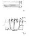
- Fig. 2shows the transmission spectrum of such an arrangement, wherein the encapsulation is not taken into account in the optical modeling.
- the total thickness of the organic layers 3 to 5was set at 78 nm (thick solid line) or 155 nm (dotted and thin solid line), and the layers 6 and 7 were considered as a ⁇ / 4 layer with the refractive index 1.38 modeled. It turns out that this arrangement at about 630nm, 540nm and 480nm each shows a high reflection. In this way, a highly asymmetric emission can be achieved with such an arrangement, although the total transmission is still greater than 60%.
Landscapes
- Physics & Mathematics (AREA)
- Optics & Photonics (AREA)
- Electroluminescent Light Sources (AREA)
- Led Devices (AREA)
Description
Translated fromGermanDie Erfindung bezieht sich auf eine transparente organische Leuchtdiode (OLED).The invention relates to a transparent organic light-emitting diode (OLED).
Organische Leuchtdioden haben sich in letzter Zeit sehr schnell entwickelt. Obwohl sie erst 1987 für aufgedampfte organische Materialien (vgl.
Da auch die Lebensdauer dieser Systeme sehr schnell gewachsen ist und inzwischen Werte von 10.000 Stunden für einige Materialsysteme bereits deutlich überschritten hat, erscheinen organische Leuchtdioden auch für Anwendungen in Beleuchtungssystemen interessant. Die wesentlichen Vorteile der organischen Leuchtdioden sind neben der möglichen hohen Effizienz, die bereits heute diejenige von Glühbirnen überschreitet und in Zukunft möglicherweise die Effizienz von Leuchtstoffröhren erreicht, die Möglichkeit, eine großflächige Beleuchtungseinheit zu realisieren, wodurch sehr blendfreies und für viele Anwendung ideal geeignetes Licht erzeugt werden kann.Since the lifespan of these systems has also grown very rapidly and has already clearly exceeded values of 10,000 hours for some material systems, organic light-emitting diodes also appear interesting for applications in lighting systems. The main advantages of the organic light-emitting diodes are, in addition to the possible high efficiency, which already exceeds that of light bulbs and possibly the future achieves the efficiency of fluorescent tubes, the possibility to realize a large-scale lighting unit, which produces very glare-free and ideal for many applications light can be.
Der übliche Aufbau für organische Leuchtdioden umfaßt ein transparentes Substrat, meistens Glas, das mit einer transparenten Anode beschichtet wird, die häufig aus Indiumzinnoxid oder Indiumthinoxid (ITO) gebildet ist. Darauf werden aktive organische Schichten abgeschieden und anschließend noch eine metallische Kathode zur elektrischen Kontaktierung aufgebracht. Werden einige Volt Spannung zwischen der metallischen Kathode und der transparenten Anode angelegt, so emittiert die Leuchtdiode durch das Substrat das Licht.The usual organic light emitting diode structure includes a transparent substrate, usually glass, which is coated with a transparent anode, often formed of indium tin oxide or indium thioxide (ITO). Then active organic layers are deposited and then applied a metal cathode for electrical contact. When a few volts of voltage are applied between the metallic cathode and the transparent anode, the LED emits light through the substrate.
Es gibt auch technische Ansätze, die es erlauben, Leuchtdioden zu konstruieren, die zumindest teilweise transparent sind. Dazu kann beispielsweise die Kathode ebenfalls mit einem transparenten leitfähigem Metall oder mit einer dünnen, teilweise transparenten Metallschicht versehen werden (vgl.
Für Beleuchtungsanwendungen hingegen ist es oft nachteilig, wenn eine transparente Leuchtdiode in beide Seiten emittiert. Andererseits wäre es sehr günstig, wenn es möglich wäre, organische Leuchtdioden zu realisieren, die transparent sind und gleichzeitig deutlich bevorzugt in eine Richtung emittieren. Bei den aus der Literatur bekannten Ansätzen sind die Leuchtstärken in beiden Richtungen annähernd gleich (vgl.
Das Buch mit dem Titel "
Aufgabe der Erfindung ist es, eine transparente organische Leuchtdiode zu schaffen, welche für Beleuchtungszwecke besser geeignet ist.The object of the invention is to provide a transparent organic light emitting diode, which is better suited for lighting purposes.
Diese Aufgabe wird durch die transparente organische Leuchtdiode nach Anspruch 1 gelöst. Vorteilhafte Ausgestaltungen der Erfindung sind Gegenstand von abhängigen Unteransprüchen.This object is achieved by the transparent organic light-emitting diode according to claim 1. Advantageous embodiments of the invention are the subject of dependent subclaims.
Mit Hilfe der Erfindung ist es ermöglicht, einerseits im ausgeschalteten Zustand der transparenten organischen Leuchtdiode eine hohe optische Transparenz im sichtbaren Spektralbereich zu erzielen. Andererseits kann die Leuchtdiode im eingeschalteten Zustand weißes oder auch farbiges Licht präferentiell in eine Richtung emittieren, wobei ein Verhältnis von etwa 4:1 erreicht oder überschritten wird. Bei der vorgeschlagenen Leuchtdiode ist eine Integration einer lichtemittierenden Schichtanordnung mit einem Stapel dielektrischer Schichten vorgesehen. Mit Hilfe dieser Anordnung werden die Wellenlängen des in der lichtemittierenden organischen Schicht erzeugten Lichtes bevorzugt in eine Richtung emittiert.With the aid of the invention, it is possible, on the one hand in the switched-off state of the transparent organic light-emitting diode, to achieve a high optical transparency in the visible spectral range. On the other hand, the light emitting diode in the on state can emit white or colored light preferentially in one direction, wherein a ratio of about 4: 1 is reached or exceeded. In the proposed light-emitting diode, an integration of a light-emitting layer arrangement with a stack of dielectric layers is provided. By means of this arrangement, the wavelengths of the light generated in the light-emitting organic layer are preferably emitted in one direction.
Der Stapel dielektrischer Schichten ist bei einer Ausführungsform so gestaltet, dass in einem begrenzten Spektralbereich, der mit dem Emissionssprektrum des in der lichtemittierenden organischen Schicht erzeugten Lichtes zumindest teilweise überlappt, ein hohes Reflexionsvermögen (>90%) aufweist, wobei ein Reflexionsvermögen von >99% ausbildbar ist mit mehreren Schichten. Hierdurch wird ein wesentlicher Teil des in der lichtemittierenden organischen Schicht, welche ihrerseits als Schichtfolge gebildet sein kann, erzeugten Lichtes nur in eine Richtung emittiert, also bevorzugt durch die obere oder die untere Elektrode.The stack of dielectric layers in one embodiment is designed to have a high reflectivity (> 90%) in a limited spectral region that at least partially overlaps the emission spectrum of the light generated in the light-emitting organic layer, with a reflectivity of> 99%. can be formed with several layers. As a result, a substantial part of the light generated in the light-emitting organic layer, which in turn can be formed as a layer sequence, is emitted only in one direction, that is to say preferably through the upper or the lower electrode.
Gleichzeitig ist die Transmission der Leuchtdiode im gesamten sichtbaren Spektralbereich sehr hoch. Dies kann beispielsweise dadurch erreicht werden, dass der Stapel dielektrischer Schichten so ausgelegt wird, dass das Reflexionsband so schmal ist, dass nur die wesentlichen Teile der Emission der lichtemittierenden organischen Schicht reflektiert werden. Die Auslegung des Stapels dielektrischer Schichten kann dadurch neben den λ/4-Schichten, die in der einfachsten Form einer solchen spiegelnden Anordnung verwendet werden, auch mehrfache dieser Dicke für eine oder beide Teilkomponenten des Schichtstapels enthalten, wodurch die spektrale Reflexionsbreite reduziert wird (vgl.
Der Stapel dielektrischer Schichten reflektiert nicht nur eine Wellenlänge sondern bevorzugt mehrere, schmale Wellenlängenbereiche. Dies kann entweder mittels der sequentiellen Abscheidung mehrerer Stapel mit verschiedenen Dicken der Einzelschichten oder mittels Ausnutzung der höheren Reflektionsordnungen eines einfachen Schichtstapels erreicht werden. Hierdurch ist beispielsweise möglich, auch eine weiß emittierende transparente organische Leuchtdiode zu realisieren.The stack of dielectric layers not only reflects one wavelength but preferably a plurality of narrow wavelength ranges. This can be achieved either by the sequential deposition of several stacks with different thicknesses of the individual layers or by utilizing the higher reflection orders of a simple layer stack. This makes it possible, for example, to realize a white emitting transparent organic light emitting diode.
Das hier vorgeschlagene Prinzip ist sehr allgemein anwendbar und ist zum Beispiel von der genauen Natur der Schichtanordnung unabhängig. Beispielsweise ist es sowohl für aus der Lösung aufgebrachte als auch für im Vakuum aufgedampfte Schichtanordnungen verwendbar. Weiterhin kann es auch für organische Leuchtdioden verwendet werden, wenn diese in einem Stapel aus zwei oder mehreren Dioden monolithisch integriert sind. Das abgestrahlte Licht wird in diesem Fall mit Hilfe mehrerer organischer Leuchtdioden erzeugt.The principle proposed here is very general and, for example, independent of the exact nature of the layer arrangement. For example, it is useful for both solution-deposited and vacuum-deposited layer arrangements. Furthermore, it can also be used for organic light-emitting diodes, if they are monolithically integrated in a stack of two or more diodes. The emitted light is generated in this case by means of several organic light-emitting diodes.
Die Erfindung wird im folgenden anhand von Ausführungsbeispielen unter Bezugnahme auf Figuren einer Zeichnung näher erläutert. Hierbei zeigen:
- Fig. 1
- eine schematische Darstellung einer transparenten Schichtanordnung für eine transparente organische Leuchtdiode; und
- Fig. 2
- ein Transmissionsspektrum für eine Ausführungsform einer Schichtanordnung nach
Fig. 1 .
- Fig. 1
- a schematic representation of a transparent layer arrangement for a transparent organic light emitting diode; and
- Fig. 2
- a transmission spectrum for an embodiment of a layer arrangement according to
Fig. 1 ,
Der organische Bereich 5 ist aus einem oder mehreren organischen Materialien gebildet und enthält mindestens eine lichtemittierende organische Schicht, in welcher beim Anlegen einer elektrischen Spannung an die untere und die obere Elektrode 3, 4 Licht erzeugt wird. Die lichtemittierende organische Schicht ist wahlweise als Einzelschicht oder Folge von Schichten gebildet, wie dieses in verschiedenen Ausführungen für organische Leuchtdioden bekannt ist. In ähnlicher Weise kann der organische Bereich 5 weitere organische Schichten umfassen, beispielsweise dotierte oder undotierte Löcher- oder Elektronentransportschichten. Auch Zwischenschichten können vorgesehen sein. Den Abschluss der transparenten Schichtanordnung bildet eine Kapselung 6, die zum Ausschluss von Umwelteinflüssen dient.The organic region 5 is formed of one or more organic materials and contains at least one organic light-emitting layer in which light is generated when an electric voltage is applied to the lower and
Eine vorteilhafte Ausführung einer Schichtanordnung nach
- 1. Träger, Substrat
- 2. Stapel aus im sichtbaren Spektralbereich transparenten Materialien (Dielektrika), beispielsweise fünf Schichten SiO2/TiO2 mit einer Dicke von jeweils λ/4
- 3. transparente Elektrode, beispielsweise ITO, Löcher injizierend (Anode)
- 3. p-dotierte, Löcher injizierende und transportierende Schicht
- 4. lichtemittierende organische Schicht (wahlweise mit Emitterfarbstoff dotiert)
- 5. n-dotierte, Elektronen injizierende und transportierende Schicht,
- 6. transparente Elektrode, Elektronen injizierend (Kathode),
- 7. Kapselung zum Ausschluß von Umwelteinflüssen.
- 1st carrier, substrate
- 2. stack of materials transparent in the visible spectral range (dielectrics), for example, five layers of SiO2 / TiO2 with a thickness of λ / 4
- 3. transparent electrode, for example ITO, injecting holes (anode)
- 3. p-doped, hole injecting and transporting layer
- 4. light-emitting organic layer (optionally doped with emitter dye)
- 5. n-doped, electron-injecting and transporting layer,
- 6. transparent electrode, injecting electrons (cathode),
- 7. Encapsulation to exclude environmental influences.
Für die Realisierung einer transparenten organischen Leuchtdioden, die in zwei oder drei Wellenlängenbereichen emittiert, können zum einen mehrere Stapel dielektrischer Schichten mit der jeweiligen Einzelschichtdicke λ/4 übereinander gelegt werden. Hierdurch werden jeweilige spektrale Bänder reflektiert und geben in der Überlagerung das gewünschte Spektrum des emittierten Lichtes.For the realization of a transparent organic light-emitting diode which emits in two or three wavelength ranges, on the one hand, a plurality of stacks of dielectric layers with the respective monolayer thickness λ / 4 can be superimposed. As a result, respective spectral bands are reflected and give in the superposition of the desired spectrum of the emitted light.
Eine weitere Möglichkeit besteht darin, höhere Ordnungen eines periodischen Stapels dielektrischer Schichten zu nutzen. Da bei einer λ/4-Anordnung diese höheren Ordnungen jeweils bei der halben Wellenlänge der nächstniedrigen Ordnung liegen, könnte so innerhalb des sichtbaren Spektralbereichs kaum eine Überlagerung mehrer Banden erreicht werden. Werden jedoch für die längste zu überlagernde Wellenlänge bereits Vielfache von λ/4-Schichtdicken verwendet, so können von einem Stapel dielektrischer Schichten mit einheitlichen Schichtdicken mehrere Spektralbereiche innerhalb des sichtbaren Lichts überlagert werden.Another possibility is to use higher orders of a periodic stack of dielectric layers. Since, with a λ / 4 arrangement, these higher orders each lie at half the wavelength of the next lower order, it would hardly be possible to achieve superimposition of several bands within the visible spectral range. However, if multiples of λ / 4 layer thicknesses are already used for the longest wavelength to be superimposed, a plurality of spectral regions within the visible light can be superposed by a stack of dielectric layers with uniform layer thicknesses.
Ein bevorzugtes Ausführungsbeispiel zeigt die in
- 1. Träger, Substrat, Glas
- 2. Stapel dielektrischer Schichten ("Distributed Bragg Reflector", DBR) aus im sichtbaren Spektralbereich transparenten Materialien (Dielektrika) mit drei Doppelschichten SiO2/TiO2 mit einer Dicke von jeweils 13λ/4
- 3. transparente Elektrode, beispielsweise ITO, Löcher injizierend (Anode), Dicke 146nm (dicke durchgezogene und gepunktete Linie in
Fig. 2 ) oder 73nm (dünne durchgezogene Linie inFig.2 ) - 3. p-dotierte, Löcher injizierende und transportierende Schicht
- 4. lichtemittierende Schicht (wahlweise mit Emitterfarbstoff dotiert)
- 5. n-dotierte Elektronen injizierende und transportierende Schicht
- 6. transparente Elektrode, Elektronen injizierend (Kathode)
- 7. Kapselung zum Ausschluß von Umwelteinflüssen.
- 1. carrier, substrate, glass
- 2. Stack of Dielectric Layers ("Distributed Bragg Reflector", DBR) made of transparent materials (dielectrics) in the visible spectral region with three double layers SiO 2 /
TiO 2 with a thickness of 13λ / 4 each - 3. transparent electrode, for example ITO, injecting holes (anode), thickness 146nm (thick solid and dotted line in
Fig. 2 ) or 73nm (thin solid line inFig.2 ) - 3. p-doped, hole injecting and transporting layer
- 4. light-emitting layer (optionally doped with emitter dye)
- 5. n-doped electron injecting and transporting layer
- 6. transparent electrode, injecting electrons (cathode)
- 7. Encapsulation to exclude environmental influences.
Die in der vorstehenden Beschreibung, den Ansprüchen und den Zeichnungen offenbarten Merkmale der Erfindung können sowohl einzeln als auch in beliebiger Kombination für die Verwirklichung der Erfindung in ihren verschiedenen Ausführungsformen von Bedeutung sein.The features of the invention disclosed in the above description, the claims and the drawings may be of importance both individually and in any combination for the realization of the invention in its various embodiments.
Claims (6)
- Transparent organic light-emitting diode with a layer arrangement in which a light-emitting organic layer is arranged between an upper and a lower electrode, the layer arrangement being transparent in a switched-off state and emitting light which is produced in the light-emitting organic layer by applying an electrical voltage to the upper and the lower electrode in a switched-on state, which light is radiated in a ratio of at least approximately 4:1 through the upper or the lower electrode, and wherein a stack, which is transparent in the visible spectral region, of dielectric layers of two or more materials with different refractive indices is arranged on the side of the upper or the lower electrodecharacterized in that the stack of dielectric layers is formed with a plurality of different spectral components corresponding to reflection bands of the light which is produced in the light-emitting organic layer as the reflection bands are formed using different reflection orders of the stack of dielectric layers, wherein a respective layer thickness of the dielectric layers is n × λ/4, wherein n= 1, 2, ... and λ is the wavelength of the emitted light.
- Transparent organic light-emitting diode according to Claim 1,characterized in that the emission spectrum of the light which is produced in the light-emitting organic layer and a spectral reflection region of the stack of dielectric layers, in which the stack of dielectric layers has a high reflecting power (>90%), are formed so as to be at least partly overlapping.
- Transparent organic light-emitting diode according to Claim 1 or 2,characterized in that the stack of dielectric layers is applied directly to the upper or the lower electrode.
- Transparent organic light-emitting diode according to any one of the preceding Claims,characterized in that the light-emitting organic layer is formed as a layer sequence with a plurality of layers.
- Transparent organic light-emitting diode according to any one of the preceding Claims,characterized in that the layer arrangement is formed to emit white light, the white light being composed of a plurality of spectral components of the light which is produced in the light-emitting organic layer.
- Transparent organic light-emitting diode according to any one of the preceding Claims,characterized in that the light-emitting organic layer is formed in an organic light-emitting diode, and that at least one further organic light-emitting diode with a further light-emitting organic layer is formed, the organic light-emitting diode and the at least one further organic light-emitting diode being stacked one on top of the other.
Priority Applications (7)
| Application Number | Priority Date | Filing Date | Title |
|---|---|---|---|
| EP05011427AEP1727221B1 (en) | 2005-05-27 | 2005-05-27 | Transparent organic light emitting diode |
| DE502005009415TDE502005009415D1 (en) | 2005-05-27 | 2005-05-27 | Transparent organic light emitting diode |
| EP06009885AEP1727222A3 (en) | 2005-05-27 | 2006-05-12 | Transparent light emitting element |
| TW095117553ATW200709733A (en) | 2005-05-27 | 2006-05-17 | Transparent light-emitting component |
| KR1020060047075AKR100812438B1 (en) | 2005-05-27 | 2006-05-25 | Transparent light-emitting component |
| US11/420,346US7598519B2 (en) | 2005-05-27 | 2006-05-25 | Transparent light-emitting component |
| JP2006148615AJP2006332064A (en) | 2005-05-27 | 2006-05-29 | Transparent light emitting parts |
Applications Claiming Priority (2)
| Application Number | Priority Date | Filing Date | Title |
|---|---|---|---|
| EP05011427AEP1727221B1 (en) | 2005-05-27 | 2005-05-27 | Transparent organic light emitting diode |
| EP05015072 | 2005-07-12 |
Publications (2)
| Publication Number | Publication Date |
|---|---|
| EP1727221A1 EP1727221A1 (en) | 2006-11-29 |
| EP1727221B1true EP1727221B1 (en) | 2010-04-14 |
Family
ID=37553487
Family Applications (2)
| Application Number | Title | Priority Date | Filing Date |
|---|---|---|---|
| EP05011427AExpired - LifetimeEP1727221B1 (en) | 2005-05-27 | 2005-05-27 | Transparent organic light emitting diode |
| EP06009885AWithdrawnEP1727222A3 (en) | 2005-05-27 | 2006-05-12 | Transparent light emitting element |
Family Applications After (1)
| Application Number | Title | Priority Date | Filing Date |
|---|---|---|---|
| EP06009885AWithdrawnEP1727222A3 (en) | 2005-05-27 | 2006-05-12 | Transparent light emitting element |
Country Status (6)
| Country | Link |
|---|---|
| US (1) | US7598519B2 (en) |
| EP (2) | EP1727221B1 (en) |
| JP (1) | JP2006332064A (en) |
| KR (1) | KR100812438B1 (en) |
| DE (1) | DE502005009415D1 (en) |
| TW (1) | TW200709733A (en) |
Families Citing this family (14)
| Publication number | Priority date | Publication date | Assignee | Title |
|---|---|---|---|---|
| US7193780B2 (en)* | 2003-08-22 | 2007-03-20 | Olympus Corporation | Optical filter and optical instrument |
| US7540978B2 (en) | 2004-08-05 | 2009-06-02 | Novaled Ag | Use of an organic matrix material for producing an organic semiconductor material, organic semiconductor material and electronic component |
| JP2012506129A (en)* | 2008-10-17 | 2012-03-08 | ブルーミンセンス エルエルシー | Transparent polarized light emitting device |
| US8637331B2 (en) | 2008-10-17 | 2014-01-28 | Bloominescence, Llc | Transparent polarized light-emitting device |
| DE102008061843B4 (en) | 2008-12-15 | 2018-01-18 | Novaled Gmbh | Heterocyclic compounds and their use in electronic and optoelectronic devices |
| KR101107178B1 (en) | 2009-07-20 | 2012-01-25 | 삼성모바일디스플레이주식회사 | Organic light emitting display |
| KR101084240B1 (en) | 2009-12-21 | 2011-11-16 | 삼성모바일디스플레이주식회사 | Organic light emitting diode display |
| WO2012138659A2 (en)* | 2011-04-05 | 2012-10-11 | University Of Florida Research Foundation, Inc. | Method and apparatus for solid state lighting window by an at least partially transparent, one-side emitting oled |
| EP2695214B1 (en) | 2011-04-05 | 2017-12-20 | University of Florida Research Foundation, Inc. | Method and apparatus for providing a window with an at least partially transparent one side emitting oled lighting and an ir sensitive photovoltaic panel |
| DE102011055233A1 (en) | 2011-11-10 | 2013-05-16 | Novaled Ag | Light emitting device for use in planar arrangement of illumination device to emit light in different applications, has electrical line connection electrically connecting contact terminal of light-emitting component with plugs and sockets |
| KR101268543B1 (en)* | 2012-01-18 | 2013-05-28 | 한국전자통신연구원 | Organic electroluminescent device |
| US10879428B2 (en) | 2012-05-17 | 2020-12-29 | Micron Technology, Inc. | Solid-state transducer devices with selective wavelength reflectors and associated systems and methods |
| US9818976B2 (en) | 2014-05-13 | 2017-11-14 | Apple Inc. | Encapsulation layers with improved reliability |
| CN106415873B (en)* | 2014-05-16 | 2018-02-16 | 应用材料公司 | Barrier layer stack, the method for manufacturing barrier layer stack and superelevation barrier layer and antireflection system |
Family Cites Families (151)
| Publication number | Priority date | Publication date | Assignee | Title |
|---|---|---|---|---|
| US1009204A (en)* | 1911-05-23 | 1911-11-21 | Andrew Winden | Transmission apparatus. |
| GB239203A (en) | 1924-09-01 | 1926-02-04 | Alessandro Tebaldi | Improvements relating to valves fitted to the pistons of internal combustion engines |
| US2463377A (en)* | 1945-05-11 | 1949-03-01 | Jennie W Turner | Brake-testing machine |
| US3644770A (en) | 1968-01-18 | 1972-02-22 | Varian Associates | Photoemitter having a p-type semiconductive substrate overlaid with cesium and n-type cesium oxide layers |
| US3673011A (en) | 1970-11-02 | 1972-06-27 | Westinghouse Electric Corp | Process for producing a cesium coated gallium arsenide photocathode |
| GB1419099A (en) | 1972-08-11 | 1975-12-24 | Thorn Electrical Ind Ltd | Manufacturing electric devices having sealed envelopes |
| US4066569A (en) | 1975-12-30 | 1978-01-03 | Hughes Aircraft Company | Dopants for dynamic scattering liquid crystals |
| JPS5931865Y2 (en) | 1978-12-26 | 1984-09-07 | 順司 小川 | concrete breaking tool |
| US4356429A (en) | 1980-07-17 | 1982-10-26 | Eastman Kodak Company | Organic electroluminescent cell |
| US4618453A (en) | 1985-05-30 | 1986-10-21 | The United States Of America As Represented By The Secretary Of The Navy | Conductive heterocyclic ladder polymers |
| US4769292A (en) | 1987-03-02 | 1988-09-06 | Eastman Kodak Company | Electroluminescent device with modified thin film luminescent zone |
| DE4024871A1 (en) | 1990-08-06 | 1992-02-13 | Basf Ag | PERLAMABLE ANTISTATIC EXPANDABLE STYRENE POLYMERISES |
| US5093698A (en) | 1991-02-12 | 1992-03-03 | Kabushiki Kaisha Toshiba | Organic electroluminescent device |
| DE4106122A1 (en) | 1991-02-27 | 1992-09-03 | Bayer Ag | NEW NAPHTHALIMIDES, THESE CONTAINING TONERS AND THE USE OF THE NEW NAPHTHALIMIDES AS ADDITIVES FOR TONER |
| JP2998268B2 (en) | 1991-04-19 | 2000-01-11 | 三菱化学株式会社 | Organic electroluminescent device |
| US5325383A (en) | 1993-05-17 | 1994-06-28 | Eastman Kodak Company | Laser diode operated in hybrid modulation modes |
| US6614161B1 (en)* | 1993-07-20 | 2003-09-02 | University Of Georgia Research Foundation, Inc. | Resonant microcavity display |
| JP3234936B2 (en)* | 1993-08-20 | 2001-12-04 | 松下電器産業株式会社 | Organic light emitting device and image display device |
| FI95574C (en) | 1994-02-16 | 1996-02-26 | Valtion Teknillinen | Electron-conducting molecular preparations |
| DE59510315D1 (en) | 1994-04-07 | 2002-09-19 | Covion Organic Semiconductors | Spiro compounds and their use as electroluminescent materials |
| US5478658A (en)* | 1994-05-20 | 1995-12-26 | At&T Corp. | Article comprising a microcavity light source |
| CA2159842A1 (en) | 1994-12-05 | 1996-06-06 | Joe A. Ortiz | Diode drive current source |
| US5707745A (en) | 1994-12-13 | 1998-01-13 | The Trustees Of Princeton University | Multicolor organic light emitting devices |
| US5703436A (en) | 1994-12-13 | 1997-12-30 | The Trustees Of Princeton University | Transparent contacts for organic devices |
| US5825543A (en)* | 1996-02-29 | 1998-10-20 | Minnesota Mining And Manufacturing Company | Diffusely reflecting polarizing element including a first birefringent phase and a second phase |
| JPH10125469A (en) | 1996-10-24 | 1998-05-15 | Tdk Corp | Organic EL device |
| US5834893A (en)* | 1996-12-23 | 1998-11-10 | The Trustees Of Princeton University | High efficiency organic light emitting devices with light directing structures |
| US5811833A (en) | 1996-12-23 | 1998-09-22 | University Of So. Ca | Electron transporting and light emitting layers based on organic free radicals |
| US6046543A (en)* | 1996-12-23 | 2000-04-04 | The Trustees Of Princeton University | High reliability, high efficiency, integratable organic light emitting devices and methods of producing same |
| EP0950254A4 (en) | 1996-12-23 | 2002-11-27 | Univ Princeton | LUMINESCENT ORGANIC DEVICE CONTAINING A PROTECTIVE LAYER |
| JPH10270171A (en) | 1997-01-27 | 1998-10-09 | Junji Kido | Organic electroluminescent device |
| US6160828A (en)* | 1997-07-18 | 2000-12-12 | The Trustees Of Princeton University | Organic vertical-cavity surface-emitting laser |
| DE19732828C2 (en) | 1997-07-30 | 2001-01-18 | Siemens Ag | Circuit arrangement for driving a light-emitting diode array |
| US6303238B1 (en) | 1997-12-01 | 2001-10-16 | The Trustees Of Princeton University | OLEDs doped with phosphorescent compounds |
| DE19756361A1 (en) | 1997-12-18 | 1999-06-24 | Philips Patentverwaltung | Organic light emitting diode with terbium complex |
| JPH11251067A (en) | 1998-03-02 | 1999-09-17 | Junji Kido | Organic electroluminescent device |
| GB9805476D0 (en) | 1998-03-13 | 1998-05-13 | Cambridge Display Tech Ltd | Electroluminescent devices |
| JP2991183B2 (en) | 1998-03-27 | 1999-12-20 | 日本電気株式会社 | Organic electroluminescence device |
| KR100582328B1 (en) | 1998-04-09 | 2006-05-23 | 이데미쓰 고산 가부시키가이샤 | Organic electroluminescent device |
| EP1018718B1 (en) | 1998-07-24 | 2005-09-14 | Seiko Epson Corporation | Display |
| JP2000075836A (en) | 1998-09-02 | 2000-03-14 | Sharp Corp | Organic EL light emitting device and driving method thereof |
| JP2000196140A (en) | 1998-12-28 | 2000-07-14 | Sharp Corp | Organic electroluminescent device and manufacturing method thereof |
| GB2347013A (en) | 1999-02-16 | 2000-08-23 | Sharp Kk | Charge-transport structures |
| US6473651B1 (en)* | 1999-03-02 | 2002-10-29 | Advanced Bionics Corporation | Fluid filled microphone balloon to be implanted in the middle ear |
| US7001536B2 (en) | 1999-03-23 | 2006-02-21 | The Trustees Of Princeton University | Organometallic complexes as phosphorescent emitters in organic LEDs |
| DE19916745A1 (en) | 1999-04-13 | 2000-10-19 | Mannesmann Vdo Ag | Light-emitting diode with organic light-emitting substances for generating light with mixed colors |
| GB2367692A (en) | 1999-06-09 | 2002-04-10 | Cambridge Display Tech Ltd | Method of producing organic light-emissive devices |
| EP1115268A1 (en) | 1999-07-07 | 2001-07-11 | Sony Corporation | Method and apparatus for manufacturing flexible organic el display |
| US6310360B1 (en) | 1999-07-21 | 2001-10-30 | The Trustees Of Princeton University | Intersystem crossing agents for efficient utilization of excitons in organic light emitting devices |
| TW465119B (en) | 1999-07-23 | 2001-11-21 | Semiconductor Energy Lab | EL display device and a method of manufacturing the same |
| BE1012802A3 (en) | 1999-07-28 | 2001-03-06 | Cockerill Rech & Dev | Electroluminescent and device manufacturing method thereof. |
| GB2353400B (en)* | 1999-08-20 | 2004-01-14 | Cambridge Display Tech Ltd | Mutiple-wavelength light emitting device and electronic apparatus |
| EP1138036A1 (en) | 1999-10-12 | 2001-10-04 | Koninklijke Philips Electronics N.V. | Led display device |
| KR100377321B1 (en) | 1999-12-31 | 2003-03-26 | 주식회사 엘지화학 | Electronic device comprising organic compound having p-type semiconducting characteristics |
| US7560175B2 (en) | 1999-12-31 | 2009-07-14 | Lg Chem, Ltd. | Electroluminescent devices with low work function anode |
| US6414661B1 (en) | 2000-02-22 | 2002-07-02 | Sarnoff Corporation | Method and apparatus for calibrating display devices and automatically compensating for loss in their efficiency over time |
| DE10009204A1 (en) | 2000-02-26 | 2001-08-30 | Univ Stuttgart | Process for controlling actively addressed OLED displays |
| US7233026B2 (en) | 2000-03-23 | 2007-06-19 | Emagin Corporation | Light extraction from color changing medium layers in organic light emitting diode devices |
| GB2361355B (en) | 2000-04-14 | 2004-06-23 | Seiko Epson Corp | Light emitting device |
| GB2361356B (en) | 2000-04-14 | 2005-01-05 | Seiko Epson Corp | Light emitting device |
| US7525165B2 (en) | 2000-04-17 | 2009-04-28 | Semiconductor Energy Laboratory Co., Ltd. | Light emitting device and manufacturing method thereof |
| TW516164B (en) | 2000-04-21 | 2003-01-01 | Semiconductor Energy Lab | Self-light emitting device and electrical appliance using the same |
| EP1158483A3 (en) | 2000-05-24 | 2003-02-05 | Eastman Kodak Company | Solid-state display with reference pixel |
| EP1160888A1 (en) | 2000-05-29 | 2001-12-05 | Sony International (Europe) GmbH | Hole transporting agents and photoelectric conversion device comprising the same |
| US6645645B1 (en) | 2000-05-30 | 2003-11-11 | The Trustees Of Princeton University | Phosphorescent organic light emitting devices |
| TWI245147B (en) | 2000-06-19 | 2005-12-11 | Nitto Denko Corp | Polarizing plate and liquid crystal display using the same |
| TW527848B (en) | 2000-10-25 | 2003-04-11 | Matsushita Electric Industrial Co Ltd | Light-emitting element and display device and lighting device utilizing thereof |
| AU2001247342A1 (en) | 2000-11-02 | 2002-05-15 | 3M Innovative Properties Company | Brightness enhancement of emissive displays |
| DE10058578C2 (en) | 2000-11-20 | 2002-11-28 | Univ Dresden Tech | Light-emitting component with organic layers |
| US6573651B2 (en) | 2000-12-18 | 2003-06-03 | The Trustees Of Princeton University | Highly efficient OLEDs using doped ambipolar conductive molecular organic thin films |
| KR100697373B1 (en)* | 2000-12-20 | 2007-03-20 | 비오이 하이디스 테크놀로지 주식회사 | Double-sided light emitting display device and manufacturing method |
| EP2073289B1 (en) | 2000-12-25 | 2010-12-29 | Samsung Mobile Display Co., Ltd. | Organic electroluminescent device |
| JP4220669B2 (en) | 2000-12-26 | 2009-02-04 | 出光興産株式会社 | Organic electroluminescence device |
| JP4644938B2 (en)* | 2001-01-15 | 2011-03-09 | ソニー株式会社 | Organic electroluminescence device |
| SG107573A1 (en) | 2001-01-29 | 2004-12-29 | Semiconductor Energy Lab | Light emitting device |
| KR100898304B1 (en) | 2001-03-02 | 2009-05-19 | 더 트러스티즈 오브 프린스턴 유니버시티 | Double dope layer, phosphorescent organic light emitting device |
| ITMI20010995A1 (en) | 2001-05-15 | 2002-11-15 | Getters Spa | CESIUM DISPENSERS AND PROCESS FOR THEIR USE |
| WO2003001569A2 (en) | 2001-06-21 | 2003-01-03 | The Trustees Of Princeton University | Organic light-emitting devices with blocking and transport layers |
| DE10135513B4 (en) | 2001-07-20 | 2005-02-24 | Novaled Gmbh | Light-emitting component with organic layers |
| JP2003043998A (en) | 2001-07-30 | 2003-02-14 | Pioneer Electronic Corp | Display device |
| US6501230B1 (en) | 2001-08-27 | 2002-12-31 | Eastman Kodak Company | Display with aging correction circuit |
| WO2003022908A1 (en) | 2001-09-04 | 2003-03-20 | Canon Kabushiki Kaisha | High-molecular compounds and organic luminescent devices |
| JPWO2003026356A1 (en)* | 2001-09-12 | 2005-01-06 | 日産化学工業株式会社 | Transparent substrate for organic electroluminescence device and device |
| DE10145492B4 (en) | 2001-09-14 | 2004-11-11 | Novaled Gmbh | Electroluminescent light emission device, in particular as a white light source |
| KR100437886B1 (en) | 2001-09-25 | 2004-06-30 | 한국과학기술원 | High extraction efficiency photonic crystal organic light emitting device |
| US6620350B2 (en) | 2001-10-01 | 2003-09-16 | Hon Hai Precision Ind. Co., Ltd. | Method for making gradient refractive index optical components |
| JP3823312B2 (en) | 2001-10-18 | 2006-09-20 | 日本電気株式会社 | Organic thin film transistor |
| US6888305B2 (en)* | 2001-11-06 | 2005-05-03 | Universal Display Corporation | Encapsulation structure that acts as a multilayer mirror |
| JP3852916B2 (en) | 2001-11-27 | 2006-12-06 | パイオニア株式会社 | Display device |
| US6734457B2 (en) | 2001-11-27 | 2004-05-11 | Semiconductor Energy Laboratory Co., Ltd. | Light emitting device |
| US7141817B2 (en) | 2001-11-30 | 2006-11-28 | Semiconductor Energy Laboratory Co., Ltd. | Light emitting device |
| DE10164016B4 (en) | 2001-12-28 | 2020-01-23 | Osram Opto Semiconductors Gmbh | Organic light emitting diode (OLED) and process for its production |
| US7274363B2 (en) | 2001-12-28 | 2007-09-25 | Pioneer Corporation | Panel display driving device and driving method |
| US7012363B2 (en) | 2002-01-10 | 2006-03-14 | Universal Display Corporation | OLEDs having increased external electroluminescence quantum efficiencies |
| US7224333B2 (en) | 2002-01-18 | 2007-05-29 | Semiconductor Energy Laboratory Co. Ltd. | Display device and driving method thereof |
| EP1479270B1 (en) | 2002-02-14 | 2006-07-05 | Koninklijke Philips Electronics N.V. | Switching device for driving a led array |
| DE10207859A1 (en) | 2002-02-20 | 2003-09-04 | Univ Dresden Tech | Doped organic semiconductor material and process for its production |
| US6833667B2 (en) | 2002-02-27 | 2004-12-21 | Matsushita Electric Industrial Co., Ltd. | Organic electroluminescence element and image forming apparatus or portable terminal unit using thereof |
| JP4046267B2 (en) | 2002-03-26 | 2008-02-13 | 株式会社半導体エネルギー研究所 | Display device |
| DE10215210B4 (en) | 2002-03-28 | 2006-07-13 | Novaled Gmbh | Transparent, thermally stable light-emitting component with organic layers |
| WO2003088271A1 (en) | 2002-04-08 | 2003-10-23 | The University Of Southern California | Doped organic carrier transport materials |
| TWI258603B (en) | 2002-04-23 | 2006-07-21 | Nitto Denko Corp | Polarized light device, polarized light source and image display apparatus using the same |
| GB2388236A (en) | 2002-05-01 | 2003-11-05 | Cambridge Display Tech Ltd | Display and driver circuits |
| JP2005524964A (en)* | 2002-05-08 | 2005-08-18 | ゼオラックス コーポレーション | Display Device Using Feedback Enhanced Light-Emitting Diode <Description of Related Applications> This application is a US Provisional Application No. 60 / 379,141 filed May 8, 2002, which is incorporated herein by reference in its entirety. ) Claim the benefit. The present application is based on US Patent Application No. “Feedback Enhanced Light-Emitting Device (FEEDBACKENHANCEDLIGHTTEMITTINGDEVICE)” filed on May 8, 2003, and “Lighting Device Using Feedback Enhanced Light-Emitting Diode” filed on May 8, 2003 ( Related to US Patent Application No. "LIGHTINGDEVICEUSING FEEDEDBACKHANHANCEDLIGHTTEMITTINGIODE", which are incorporated herein by reference in their entirety. |
| DE10224021B4 (en) | 2002-05-24 | 2006-06-01 | Novaled Gmbh | Phosphorescent light emitting device with organic layers |
| US6670772B1 (en) | 2002-06-27 | 2003-12-30 | Eastman Kodak Company | Organic light emitting diode display with surface plasmon outcoupling |
| DE10229231B9 (en) | 2002-06-28 | 2006-05-11 | Osram Opto Semiconductors Gmbh | A method of manufacturing a radiation emitting and / or receiving semiconductor chip having a radiation input and / or output microstructure |
| DE10228939A1 (en) | 2002-06-28 | 2004-01-15 | Philips Intellectual Property & Standards Gmbh | Electroluminescent device with transparent cathode |
| KR100978012B1 (en)* | 2002-06-28 | 2010-08-25 | 코닌클리케 필립스 일렉트로닉스 엔.브이. | Electroluminescent Devices with Transparent Cathodes |
| KR100480442B1 (en)* | 2002-08-17 | 2005-04-06 | 한국과학기술연구원 | White organic light-emitting materials prepared by light-doping and electroluminescent devices using the same |
| ITMI20021904A1 (en) | 2002-09-06 | 2004-03-07 | Getters Spa | ACCESSORY ELEMENT FOR ALKALINE METAL DISPENSERS |
| TW556446B (en) | 2002-09-11 | 2003-10-01 | Opto Tech Corp | Organic light-emitting device and the manufacturing method thereof |
| JP2005539252A (en) | 2002-09-16 | 2005-12-22 | コーニンクレッカ フィリップス エレクトロニクス エヌ ヴィ | Display device |
| JP4288918B2 (en) | 2002-09-26 | 2009-07-01 | セイコーエプソン株式会社 | ORGANIC EL PANEL AND ITS MANUFACTURING METHOD, ELECTRO-OPTICAL PANEL USING THE SAME, AND ELECTRONIC DEVICE |
| JP3963811B2 (en) | 2002-09-30 | 2007-08-22 | 富士フイルム株式会社 | Organic electroluminescence device |
| US6965197B2 (en) | 2002-10-01 | 2005-11-15 | Eastman Kodak Company | Organic light-emitting device having enhanced light extraction efficiency |
| DE10251986A1 (en) | 2002-11-08 | 2004-05-19 | Covion Organic Semiconductors Gmbh | Ring-halogenated organo-palladium and organo-platinum compounds with ortho-metallated 2-phenylpyridyl or 2-heteroaryl-pyridyl groups, used in electrical or electronic components, e.g. light-emitting diodes |
| DE10262143B4 (en) | 2002-12-20 | 2011-01-20 | Ksg Leiterplatten Gmbh | Light-emitting arrangement |
| JP2004207136A (en) | 2002-12-26 | 2004-07-22 | Nitto Denko Corp | Surface light source and display device using the same |
| WO2004059606A2 (en) | 2002-12-30 | 2004-07-15 | Koninklijke Philips Electronics N.V. | Line-at-a-time addressed display and drive method |
| JP2004247106A (en) | 2003-02-12 | 2004-09-02 | Fuji Electric Holdings Co Ltd | Organic EL element and method of manufacturing organic EL element |
| JP3910926B2 (en) | 2003-02-26 | 2007-04-25 | 株式会社東芝 | Method for producing transparent substrate for display device |
| US6837939B1 (en) | 2003-07-22 | 2005-01-04 | Eastman Kodak Company | Thermal physical vapor deposition source using pellets of organic material for making OLED displays |
| US7193780B2 (en) | 2003-08-22 | 2007-03-20 | Olympus Corporation | Optical filter and optical instrument |
| JP4468667B2 (en)* | 2003-08-22 | 2010-05-26 | オリンパス株式会社 | Optical filter and optical apparatus |
| DE10339772B4 (en) | 2003-08-27 | 2006-07-13 | Novaled Gmbh | Light emitting device and method for its production |
| JP2005108672A (en) | 2003-09-30 | 2005-04-21 | Seiko Instruments Inc | El element and display apparatus using it |
| US7655961B2 (en) | 2003-10-02 | 2010-02-02 | Maxdem Incorporated | Organic diodes and materials |
| DE10347856B8 (en) | 2003-10-10 | 2006-10-19 | Colorado State University Research Foundation, Fort Collins | Semiconductor doping |
| WO2005051525A1 (en)* | 2003-11-25 | 2005-06-09 | Polyvalor, Limited Partnership | Permeation barrier coating or layer with modulated properties and methods of making the same |
| CN1638585A (en) | 2003-12-26 | 2005-07-13 | 日东电工株式会社 | Electroluminescence device, planar light source and display using the same |
| DE102004002587B4 (en) | 2004-01-16 | 2006-06-01 | Novaled Gmbh | Image element for an active matrix display |
| DE102004010954A1 (en) | 2004-03-03 | 2005-10-06 | Novaled Gmbh | Use of a metal complex as an n-dopant for an organic semiconductive matrix material, organic semiconductor material and electronic component |
| JP2004235168A (en) | 2004-05-20 | 2004-08-19 | Toyota Industries Corp | Organic electroluminescent element |
| WO2005123754A2 (en) | 2004-06-14 | 2005-12-29 | Georgia Tech Research Corporation | Transition-metal charge-transport materials, methods of fabrication thereof, and methods of use thereof |
| US20060044227A1 (en) | 2004-06-18 | 2006-03-02 | Eastman Kodak Company | Selecting adjustment for OLED drive voltage |
| DE102004035965B4 (en) | 2004-07-23 | 2007-07-26 | Novaled Ag | Top-emitting, electroluminescent component with at least one organic layer |
| US7540978B2 (en) | 2004-08-05 | 2009-06-02 | Novaled Ag | Use of an organic matrix material for producing an organic semiconductor material, organic semiconductor material and electronic component |
| DE112005002603A5 (en) | 2004-08-13 | 2007-08-09 | Novaled Gmbh | Layer arrangement for a light-emitting component |
| CN1738069A (en) | 2004-08-17 | 2006-02-22 | 国际商业机器公司 | Electronic device manufacturing method and electronic device whose electrodes have enhanced injection characteristics |
| DE102004041371B4 (en) | 2004-08-25 | 2007-08-02 | Novaled Ag | Component based on an organic light emitting diode device and method for manufacturing |
| DE102004045871B4 (en) | 2004-09-20 | 2006-11-23 | Novaled Gmbh | Method and circuit arrangement for aging compensation of organic light emitting diodes |
| EP1648042B1 (en) | 2004-10-07 | 2007-05-02 | Novaled AG | A method for doping a semiconductor material with cesium |
| EP2264806B1 (en) | 2005-04-13 | 2019-03-27 | Novaled GmbH | Assembly for an organic pin-type LED and manufacturing method |
| EP1729346A1 (en) | 2005-06-01 | 2006-12-06 | Novaled AG | Light-emitting device with an electrode arrangement |
| DE502005003742D1 (en) | 2005-06-14 | 2008-05-29 | Novaled Ag | A method of operating an organic light emitting device and organic light emitting device |
| EP1739765A1 (en) | 2005-07-01 | 2007-01-03 | Novaled AG | Organic light-emitting diode and stack of organic light emitting diodes |
| DE502005005126D1 (en) | 2005-08-11 | 2008-10-02 | Novaled Ag | Method for producing a top-emitting component and use |
| US7919010B2 (en) | 2005-12-22 | 2011-04-05 | Novaled Ag | Doped organic semiconductor material |
| EP1837926B1 (en) | 2006-03-21 | 2008-05-07 | Novaled AG | Heterocyclic radicals or diradicals and their dimers, oligomers, polymers, di-spiro and polycyclic derivatives as well as their use in organic semiconductor materials and electronic devices. |
| DE102006059509B4 (en) | 2006-12-14 | 2012-05-03 | Novaled Ag | Organic light-emitting element |
- 2005
- 2005-05-27EPEP05011427Apatent/EP1727221B1/ennot_activeExpired - Lifetime
- 2005-05-27DEDE502005009415Tpatent/DE502005009415D1/ennot_activeExpired - Lifetime
- 2006
- 2006-05-12EPEP06009885Apatent/EP1727222A3/ennot_activeWithdrawn
- 2006-05-17TWTW095117553Apatent/TW200709733A/enunknown
- 2006-05-25KRKR1020060047075Apatent/KR100812438B1/enactiveActive
- 2006-05-25USUS11/420,346patent/US7598519B2/enactiveActive
- 2006-05-29JPJP2006148615Apatent/JP2006332064A/enactivePending
Non-Patent Citations (1)
| Title |
|---|
| M. A. MACLEOD: "Thin film optical films, 3rd edition", 2001, INSTITUTE OF PHYSICS, IOP, BOSTON* |
Also Published As
| Publication number | Publication date |
|---|---|
| DE502005009415D1 (en) | 2010-05-27 |
| US7598519B2 (en) | 2009-10-06 |
| EP1727222A2 (en) | 2006-11-29 |
| KR20060122742A (en) | 2006-11-30 |
| KR100812438B1 (en) | 2008-03-10 |
| US20060284170A1 (en) | 2006-12-21 |
| JP2006332064A (en) | 2006-12-07 |
| TW200709733A (en) | 2007-03-01 |
| EP1727222A3 (en) | 2008-11-19 |
| EP1727221A1 (en) | 2006-11-29 |
Similar Documents
| Publication | Publication Date | Title |
|---|---|---|
| EP1727222A2 (en) | Transparent light emitting element | |
| DE102006059509B4 (en) | Organic light-emitting element | |
| WO2006097069A1 (en) | Transparent light-emitting component | |
| DE69732713T2 (en) | LIGHT-EMITTING OBJECTS WITH LIGHT-REFLECTIVE STRUCTURES | |
| EP2816628B1 (en) | Light-emitting organic component and arrangement having a plurality of light-emitting organic components | |
| DE102018129857A1 (en) | Organic light-emitting diode display | |
| DE60223443T2 (en) | Organic light-emitting diode with high contrast ratio | |
| EP0854662A2 (en) | Electroluminescent colour display panel | |
| DE112012003937T5 (en) | Organic electroluminescent element | |
| DE102012202839B4 (en) | Organic light emitting diode | |
| DE102007022090A1 (en) | Light-emitting component | |
| DE102015205198A1 (en) | White light emitting organic device | |
| DE102004020245A1 (en) | Organic, electro-optical element with increased coupling efficiency | |
| WO2003026030A1 (en) | White light led with multicolor light-emitting layers of macroscopic structure widths, arranged on a light-diffusing glass | |
| EP1739765A1 (en) | Organic light-emitting diode and stack of organic light emitting diodes | |
| DE10228939A1 (en) | Electroluminescent device with transparent cathode | |
| WO2006024278A1 (en) | Top-emitting, electroluminescent component comprising frequency conversion centers | |
| EP2732482A1 (en) | Light module with controllable light guidance | |
| EP2165378A1 (en) | Organic component vertically emitting white light | |
| WO2007059945A1 (en) | Light-emitting component | |
| WO2012146633A1 (en) | Light-emitting element having an oled or qled | |
| DE102010023619A1 (en) | Organic bottom-emitting device | |
| WO2015082486A1 (en) | Organic light-emitting component | |
| DE102014103675A1 (en) | Organic light emitting device | |
| DE102008018663A1 (en) | Electro-optical organic component |
Legal Events
| Date | Code | Title | Description |
|---|---|---|---|
| PUAI | Public reference made under article 153(3) epc to a published international application that has entered the european phase | Free format text:ORIGINAL CODE: 0009012 | |
| 17P | Request for examination filed | Effective date:20060518 | |
| AK | Designated contracting states | Kind code of ref document:A1 Designated state(s):AT BE BG CH CY CZ DE DK EE ES FI FR GB GR HU IE IS IT LI LT LU MC NL PL PT RO SE SI SK TR | |
| AX | Request for extension of the european patent | Extension state:AL BA HR LV MK YU | |
| 17Q | First examination report despatched | Effective date:20070207 | |
| RAP1 | Party data changed (applicant data changed or rights of an application transferred) | Owner name:NOVALED AG | |
| AKX | Designation fees paid | Designated state(s):DE FR GB NL | |
| GRAP | Despatch of communication of intention to grant a patent | Free format text:ORIGINAL CODE: EPIDOSNIGR1 | |
| RTI1 | Title (correction) | Free format text:TRANSPARENT ORGANIC LIGHT EMITTING DIODE | |
| GRAS | Grant fee paid | Free format text:ORIGINAL CODE: EPIDOSNIGR3 | |
| GRAA | (expected) grant | Free format text:ORIGINAL CODE: 0009210 | |
| AK | Designated contracting states | Kind code of ref document:B1 Designated state(s):DE FR GB NL | |
| REG | Reference to a national code | Ref country code:GB Ref legal event code:FG4D Free format text:NOT ENGLISH | |
| REF | Corresponds to: | Ref document number:502005009415 Country of ref document:DE Date of ref document:20100527 Kind code of ref document:P | |
| REG | Reference to a national code | Ref country code:NL Ref legal event code:VDEP Effective date:20100414 | |
| PG25 | Lapsed in a contracting state [announced via postgrant information from national office to epo] | Ref country code:NL Free format text:LAPSE BECAUSE OF FAILURE TO SUBMIT A TRANSLATION OF THE DESCRIPTION OR TO PAY THE FEE WITHIN THE PRESCRIBED TIME-LIMIT Effective date:20100414 | |
| PLBE | No opposition filed within time limit | Free format text:ORIGINAL CODE: 0009261 | |
| STAA | Information on the status of an ep patent application or granted ep patent | Free format text:STATUS: NO OPPOSITION FILED WITHIN TIME LIMIT | |
| 26N | No opposition filed | Effective date:20110117 | |
| REG | Reference to a national code | Ref country code:FR Ref legal event code:PLFP Year of fee payment:12 | |
| REG | Reference to a national code | Ref country code:FR Ref legal event code:PLFP Year of fee payment:13 | |
| REG | Reference to a national code | Ref country code:DE Ref legal event code:R082 Ref document number:502005009415 Country of ref document:DE Representative=s name:BOEHMERT & BOEHMERT ANWALTSPARTNERSCHAFT MBB -, DE Ref country code:DE Ref legal event code:R081 Ref document number:502005009415 Country of ref document:DE Owner name:NOVALED GMBH, DE Free format text:FORMER OWNER: NOVALED AG, 01307 DRESDEN, DE | |
| REG | Reference to a national code | Ref country code:FR Ref legal event code:PLFP Year of fee payment:14 | |
| PGFP | Annual fee paid to national office [announced via postgrant information from national office to epo] | Ref country code:GB Payment date:20220407 Year of fee payment:18 Ref country code:FR Payment date:20220408 Year of fee payment:18 | |
| REG | Reference to a national code | Ref country code:DE Ref legal event code:R079 Ref document number:502005009415 Country of ref document:DE Free format text:PREVIOUS MAIN CLASS: H01L0051520000 Ipc:H10K0050800000 | |
| P01 | Opt-out of the competence of the unified patent court (upc) registered | Effective date:20230515 | |
| GBPC | Gb: european patent ceased through non-payment of renewal fee | Effective date:20230527 | |
| PG25 | Lapsed in a contracting state [announced via postgrant information from national office to epo] | Ref country code:GB Free format text:LAPSE BECAUSE OF NON-PAYMENT OF DUE FEES Effective date:20230527 | |
| PG25 | Lapsed in a contracting state [announced via postgrant information from national office to epo] | Ref country code:FR Free format text:LAPSE BECAUSE OF NON-PAYMENT OF DUE FEES Effective date:20230531 | |
| PGFP | Annual fee paid to national office [announced via postgrant information from national office to epo] | Ref country code:DE Payment date:20240328 Year of fee payment:20 | |
| REG | Reference to a national code | Ref country code:DE Ref legal event code:R071 Ref document number:502005009415 Country of ref document:DE |