EP1727177B1 - Process for producing a photoelectric layered member and layered member - Google Patents
Process for producing a photoelectric layered member and layered memberDownload PDFInfo
- Publication number
- EP1727177B1 EP1727177B1EP05720151.9AEP05720151AEP1727177B1EP 1727177 B1EP1727177 B1EP 1727177B1EP 05720151 AEP05720151 AEP 05720151AEP 1727177 B1EP1727177 B1EP 1727177B1
- Authority
- EP
- European Patent Office
- Prior art keywords
- layer
- substrate
- nitride semiconductor
- semiconductor crystal
- crystal layer
- Prior art date
- Legal status (The legal status is an assumption and is not a legal conclusion. Google has not performed a legal analysis and makes no representation as to the accuracy of the status listed.)
- Expired - Lifetime
Links
- 238000000034methodMethods0.000titleclaimsdescription19
- 239000010410layerSubstances0.000claimsdescription125
- 239000013078crystalSubstances0.000claimsdescription80
- 239000000758substrateSubstances0.000claimsdescription66
- 239000004065semiconductorSubstances0.000claimsdescription61
- 150000004767nitridesChemical class0.000claimsdescription51
- 239000000463materialSubstances0.000claimsdescription31
- 239000011521glassSubstances0.000claimsdescription20
- 238000004519manufacturing processMethods0.000claimsdescription19
- 239000012790adhesive layerSubstances0.000claimsdescription13
- 229910002704AlGaNInorganic materials0.000claimsdescription7
- 239000011241protective layerSubstances0.000claimsdescription5
- 239000000853adhesiveSubstances0.000claimsdescription4
- 230000001070adhesive effectEffects0.000claimsdescription4
- 229910001218Gallium arsenideInorganic materials0.000claimsdescription2
- 229910052783alkali metalInorganic materials0.000claimsdescription2
- 150000001340alkali metalsChemical class0.000claimsdescription2
- -1polytetrafluoroethylenePolymers0.000claims2
- 229920001343polytetrafluoroethylenePolymers0.000claims2
- 239000004810polytetrafluoroethyleneSubstances0.000claims2
- 239000000126substanceSubstances0.000claims1
- 230000010287polarizationEffects0.000description14
- 238000005530etchingMethods0.000description9
- XUIMIQQOPSSXEZ-UHFFFAOYSA-NSiliconChemical compound[Si]XUIMIQQOPSSXEZ-UHFFFAOYSA-N0.000description8
- 230000000694effectsEffects0.000description8
- 238000010586diagramMethods0.000description6
- 229910052710siliconInorganic materials0.000description5
- 239000010703siliconSubstances0.000description5
- 229910052594sapphireInorganic materials0.000description3
- 239000010980sapphireSubstances0.000description3
- 230000002269spontaneous effectEffects0.000description3
- QTBSBXVTEAMEQO-UHFFFAOYSA-NAcetic acidChemical compoundCC(O)=OQTBSBXVTEAMEQO-UHFFFAOYSA-N0.000description2
- VYPSYNLAJGMNEJ-UHFFFAOYSA-NSilicium dioxideChemical compoundO=[Si]=OVYPSYNLAJGMNEJ-UHFFFAOYSA-N0.000description2
- 239000004809TeflonSubstances0.000description2
- 229920006362Teflon®Polymers0.000description2
- 238000004140cleaningMethods0.000description2
- 238000002109crystal growth methodMethods0.000description2
- 238000009792diffusion processMethods0.000description2
- 238000009826distributionMethods0.000description2
- 230000002349favourable effectEffects0.000description2
- 239000002344surface layerSubstances0.000description2
- FYYHWMGAXLPEAU-UHFFFAOYSA-NMagnesiumChemical compound[Mg]FYYHWMGAXLPEAU-UHFFFAOYSA-N0.000description1
- GRYLNZFGIOXLOG-UHFFFAOYSA-NNitric acidChemical compoundO[N+]([O-])=OGRYLNZFGIOXLOG-UHFFFAOYSA-N0.000description1
- 230000001133accelerationEffects0.000description1
- 239000000370acceptorSubstances0.000description1
- 239000003513alkaliSubstances0.000description1
- 229910052782aluminiumInorganic materials0.000description1
- 238000005452bendingMethods0.000description1
- 238000005229chemical vapour depositionMethods0.000description1
- 229910052804chromiumInorganic materials0.000description1
- 238000012790confirmationMethods0.000description1
- 239000002178crystalline materialSubstances0.000description1
- 230000003628erosive effectEffects0.000description1
- 238000011156evaluationMethods0.000description1
- 229910052733galliumInorganic materials0.000description1
- 238000011835investigationMethods0.000description1
- 150000002500ionsChemical class0.000description1
- 229910052749magnesiumInorganic materials0.000description1
- 239000011777magnesiumSubstances0.000description1
- 238000002488metal-organic chemical vapour depositionMethods0.000description1
- 229910052759nickelInorganic materials0.000description1
- 229910017604nitric acidInorganic materials0.000description1
- 238000005036potential barrierMethods0.000description1
- 238000012545processingMethods0.000description1
- 235000012239silicon dioxideNutrition0.000description1
- 239000000377silicon dioxideSubstances0.000description1
- 238000007740vapor depositionMethods0.000description1
Images


Classifications
- H—ELECTRICITY
- H10—SEMICONDUCTOR DEVICES; ELECTRIC SOLID-STATE DEVICES NOT OTHERWISE PROVIDED FOR
- H10F—INORGANIC SEMICONDUCTOR DEVICES SENSITIVE TO INFRARED RADIATION, LIGHT, ELECTROMAGNETIC RADIATION OF SHORTER WAVELENGTH OR CORPUSCULAR RADIATION
- H10F71/00—Manufacture or treatment of devices covered by this subclass
- H10F71/127—The active layers comprising only Group III-V materials, e.g. GaAs or InP
- H10F71/1278—The active layers comprising only Group III-V materials, e.g. GaAs or InP comprising nitrides, e.g. GaN
- H—ELECTRICITY
- H01—ELECTRIC ELEMENTS
- H01J—ELECTRIC DISCHARGE TUBES OR DISCHARGE LAMPS
- H01J1/00—Details of electrodes, of magnetic control means, of screens, or of the mounting or spacing thereof, common to two or more basic types of discharge tubes or lamps
- H01J1/02—Main electrodes
- H01J1/34—Photo-emissive cathodes
- C—CHEMISTRY; METALLURGY
- C30—CRYSTAL GROWTH
- C30B—SINGLE-CRYSTAL GROWTH; UNIDIRECTIONAL SOLIDIFICATION OF EUTECTIC MATERIAL OR UNIDIRECTIONAL DEMIXING OF EUTECTOID MATERIAL; REFINING BY ZONE-MELTING OF MATERIAL; PRODUCTION OF A HOMOGENEOUS POLYCRYSTALLINE MATERIAL WITH DEFINED STRUCTURE; SINGLE CRYSTALS OR HOMOGENEOUS POLYCRYSTALLINE MATERIAL WITH DEFINED STRUCTURE; AFTER-TREATMENT OF SINGLE CRYSTALS OR A HOMOGENEOUS POLYCRYSTALLINE MATERIAL WITH DEFINED STRUCTURE; APPARATUS THEREFOR
- C30B29/00—Single crystals or homogeneous polycrystalline material with defined structure characterised by the material or by their shape
- C30B29/10—Inorganic compounds or compositions
- C30B29/40—AIIIBV compounds wherein A is B, Al, Ga, In or Tl and B is N, P, As, Sb or Bi
- C30B29/403—AIII-nitrides
- H—ELECTRICITY
- H01—ELECTRIC ELEMENTS
- H01J—ELECTRIC DISCHARGE TUBES OR DISCHARGE LAMPS
- H01J40/00—Photoelectric discharge tubes not involving the ionisation of a gas
- H01J40/02—Details
- H01J40/04—Electrodes
- H01J40/06—Photo-emissive cathodes
- H—ELECTRICITY
- H01—ELECTRIC ELEMENTS
- H01J—ELECTRIC DISCHARGE TUBES OR DISCHARGE LAMPS
- H01J9/00—Apparatus or processes specially adapted for the manufacture, installation, removal, maintenance of electric discharge tubes, discharge lamps, or parts thereof; Recovery of material from discharge tubes or lamps
- H01J9/02—Manufacture of electrodes or electrode systems
- H01J9/12—Manufacture of electrodes or electrode systems of photo-emissive cathodes; of secondary-emission electrodes
- H—ELECTRICITY
- H10—SEMICONDUCTOR DEVICES; ELECTRIC SOLID-STATE DEVICES NOT OTHERWISE PROVIDED FOR
- H10F—INORGANIC SEMICONDUCTOR DEVICES SENSITIVE TO INFRARED RADIATION, LIGHT, ELECTROMAGNETIC RADIATION OF SHORTER WAVELENGTH OR CORPUSCULAR RADIATION
- H10F71/00—Manufacture or treatment of devices covered by this subclass
- H10F71/127—The active layers comprising only Group III-V materials, e.g. GaAs or InP
- H10F71/1272—The active layers comprising only Group III-V materials, e.g. GaAs or InP comprising at least three elements, e.g. GaAlAs or InGaAsP
- H10F71/1274—The active layers comprising only Group III-V materials, e.g. GaAs or InP comprising at least three elements, e.g. GaAlAs or InGaAsP comprising nitrides, e.g. InGaN or InGaAlN
- H—ELECTRICITY
- H10—SEMICONDUCTOR DEVICES; ELECTRIC SOLID-STATE DEVICES NOT OTHERWISE PROVIDED FOR
- H10F—INORGANIC SEMICONDUCTOR DEVICES SENSITIVE TO INFRARED RADIATION, LIGHT, ELECTROMAGNETIC RADIATION OF SHORTER WAVELENGTH OR CORPUSCULAR RADIATION
- H10F71/00—Manufacture or treatment of devices covered by this subclass
- H10F71/127—The active layers comprising only Group III-V materials, e.g. GaAs or InP
- H10F71/1276—The active layers comprising only Group III-V materials, e.g. GaAs or InP comprising growth substrates not made of Group III-V materials
- Y—GENERAL TAGGING OF NEW TECHNOLOGICAL DEVELOPMENTS; GENERAL TAGGING OF CROSS-SECTIONAL TECHNOLOGIES SPANNING OVER SEVERAL SECTIONS OF THE IPC; TECHNICAL SUBJECTS COVERED BY FORMER USPC CROSS-REFERENCE ART COLLECTIONS [XRACs] AND DIGESTS
- Y10—TECHNICAL SUBJECTS COVERED BY FORMER USPC
- Y10S—TECHNICAL SUBJECTS COVERED BY FORMER USPC CROSS-REFERENCE ART COLLECTIONS [XRACs] AND DIGESTS
- Y10S117/00—Single-crystal, oriented-crystal, and epitaxy growth processes; non-coating apparatus therefor
- Y10S117/901—Levitation, reduced gravity, microgravity, space
- Y10S117/902—Specified orientation, shape, crystallography, or size of seed or substrate
- Y—GENERAL TAGGING OF NEW TECHNOLOGICAL DEVELOPMENTS; GENERAL TAGGING OF CROSS-SECTIONAL TECHNOLOGIES SPANNING OVER SEVERAL SECTIONS OF THE IPC; TECHNICAL SUBJECTS COVERED BY FORMER USPC CROSS-REFERENCE ART COLLECTIONS [XRACs] AND DIGESTS
- Y10—TECHNICAL SUBJECTS COVERED BY FORMER USPC
- Y10S—TECHNICAL SUBJECTS COVERED BY FORMER USPC CROSS-REFERENCE ART COLLECTIONS [XRACs] AND DIGESTS
- Y10S117/00—Single-crystal, oriented-crystal, and epitaxy growth processes; non-coating apparatus therefor
- Y10S117/915—Separating from substrate
Definitions
- the present inventionrelates to a layered member and a manufacturing method for a layered member comprising a layer formed by a nitride type semiconductor material.
- An example of a layered member comprising a layer formed by a nitride type semiconductor materialis a photoelectric surface comprising a GaN layer as an active layer (for instance, see cited patent 1).
- WO 03/107386relates to a method for manufacturing a semiconductor photoelectric surface and a photodetecting tube using the semiconductor photoelectric surface.
- Cited patent 1Japanese Patent Application Laid-open No. H10-241554 .
- An object of the present inventionis to provide a layered member and a manufacturing method for a layered member which can further increase quantum efficiency and achieved lower costs.
- the present inventorshave performed evaluations from many aspects.
- sapphire substrateshave a high material cost, and an extremely long time is required when mechanically processing so the price becomes even higher.
- silicon substrates with high qualityare supplied at low cost in large sheets.
- the productivity of the photoelectric surface processis excellent compared to sapphire substrates.
- the markethas been demanding lower prices as well as demanding higher performance. From this point of view, there is demand to satisfy both of these requirements. Therefore the present inventors first focused attention to the polarization of nitride type semiconductor materials.
- Nitride type semiconductor materialshave material specific polarization properties which include spontaneous polarization along the c axis of the crystal and piezo polarization.
- material specific polarization propertiesinclude spontaneous polarization along the c axis of the crystal and piezo polarization.
- the positive chargewill increase above the surface level because of polarization, and therefore strong band bending will occur at the surface. Therefore the quantum efficiency of the active layer is increased by utilizing the surface emission of the photoelectrons.
- a built-in field and active layerwill be formed and the diffusion length will be extended.
- the topmost layer of the photoelectric surfacemust be a -c surface (surface in the negative c polar direction, N surface direction) and a very smooth surface must be achieved.
- the MOCVD growth method used for normal sapphire substratessurface orientation of main surface is (0001)c
- the +c planeplane in the positive c polar direction, plane in the Group III element surface direction
- the growth of the -c surfaceis difficult to control and a highly smooth surface can not be obtained.
- the present inventorsAs a result of further investigations into this point by the present inventors, the following finding was made. Namely, when a wafer is obtained using this crystal growth method, the surface on the opposite side of the +c polar direction (hereinafter, +c surface) is the -c polar direction surface (hereinafter, -c surface). Furthermore, it was discovered that the plane orientation of the crystal growth substrate used to grow the nitride type semiconductor material also has an effect of achieving a smooth surface. The present invention was achieved based on these findings.
- the manufacturing method of the layered member of the present inventionis defined in claim 1.
- the plane orientationis (111) for the main surface of the substrate for crystal growth which forms a nitride semiconductor crystal layer by crystal growth through a buffer layer, so the surface of the substrate side for growing crystals of the nitride type semiconductor material can be the -c layer. Furthermore, the substrate for growing crystals is removed after the nitride semiconductor crystal layer and the substrate are adhesively fixed together by an adhesive layer so the -c surface of the buffer layer can be the topmost surface layer.
- the buffer layeris removed, so the -c layer of the nitride semiconductor crystal layer can be the topmost surface layer.
- the layered member manufacturing method of the present inventionpreferably further comprises, after the step of removing the substrate for crystal growth, a step of causing crystal growth of the semiconductor material on the negative c polar surface of the buffer layer. Crystal growth will occur on the negative c polar surface so favorable crystal growth is possible.
- the layered member manufacturing method of the present inventionpreferably further comprises, after the step of removing the buffer layer, a step of causing crystal growth of the semiconductor material on the negative c polar surface of the nitride semiconductor crystal layer. Crystal growth will occur on the negative c polar surface so favorable crystal growth is possible.
- the layered member manufacturing method of the present inventionpreferably further comprises, prior to the step of removing the substrate for crystal growth, a step of forming a protective layer which covers at least the periphery of the substrate.
- the periphery of the substratewill be covered by a protective layer, and therefore, when removing the buffer layer and the substrate for forming crystals by etching, for instance, erosion of the substrate can be reduced.
- the layered member of the present inventionis defined in claim 12.
- the direction from the first surface to the second surface of the nitride semiconductor crystal layeris the negative c polar direction, so the second surface will be the -c surface.
- the first surfaceis an incidence plane where the light enters
- the second surfaceis an emission plane which emits the photoelectron
- the substrateis a glass substrate formed to transmit light
- the layered memberis preferably used as a photoelectric surface member which emits photoelectrons which have been excited by incident light.
- the second surfaceis the emission plane, so the emission plane of the photoelectric surface member can be the -c surface.
- a layered membercan be produced where the topmost layer is the -c surface. Therefore, a layered member and a manufacturing method for a layered member which can have even higher quantum efficiency can be provided.
- 1a- photoelectric surface member10- nitride semiconductor crystal layer, 12- adhesive layer, 14- glass substrate, 16- cathode electrode, 18- Cs-O layer.
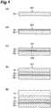
- Fig. 1A-E and Fig. 2A-Eare cross-section diagrams for describing the manufacturing steps of the photoelectric surface member.
- a silicon (111) substratewas prepared as the substrate 50 for crystal growth (see Fig. 1A ).
- the substrate 50 for crystal growthwhich is a silicon (111) substrate is a crystalline material and the surface orientation of the main surface 501 is (111).
- Al x Ga 1-x N (0 ⁇ X ⁇ 1)is grown to approximately several tens of nanometers, and buffer layer 52 is formed on the main surface 501 of the silicon (111) substrate 50 (see Fig. 1B ).
- a nitride semiconductor crystal layer 10 with a thickness of approximately several hundred nanometersis formed on the main surface 521 of the buffer layer 52 by epitaxial growth using a Group III-V nitride semiconductor gas material comprising Ga and N (see Fig. 1C ).
- the nitride semiconductor crystal layer 10is doped with magnesium to a level between approximately E19 and E20.
- the surface orientation of the main surface 501 of the substrate 50 for crystal growthis (111), so the first surface 101 of the nitride semiconductor crystal layer 10 is the +c surface, and the second surface 102 is the -c surface.
- a layer of silicon dioxidewas overlaid with a thickness of between 100 and 200 nm on to the first surface 101 of the nitride semiconductor crystal layer 10 using the CVD method to form the adhesive layer 12 (see Fig. 1D ).
- the glass substrate 14was prepared.
- the glass substrate 14preferably has a thermal expansion coefficient similar to the thermal expansion coefficient of the substrate 50 for crystal growth, and preferably contains prescribed alkali ion elements. Corning's 9741 and Schott's 8337B are examples of these types of glass substrates 14.
- the glass substrate 14 and a multilayered sheet with the configuration shown in Fig. 1Dwere rapidly heated to the glass softening point while the main surface 121 of the adhesive layer 12 was brought into contact with the glass substrate 14.
- a prescribed loadingwas applied, and the multilayered sheet and the glass substrate 14 were thermocompression bonded through the adhesive layer 12 (see Fig. 1E ).
- etchingwas performed at room temperature using (1 HF + 1 HNO 3 + 1 CH 3 COOH) as the etchant.
- the substrate 50 for crystal growthwas etched by this etching process, and the etching was stopped by the buffer layer 52 (see Fig. 2B ). Therefore, the buffer layer 52 acted as the stopping layer.
- etchingwas performed using (1 KOH + 10 H 2 O + 0.01 H 2 O 2 ) as the etchant to remove the buffer layer 52 (see Fig. 2C ).
- the etching speed of +c surface AlN and GaNis extremely slow, but with this embodiment, the -c surface side is etched so etching can be performed using the aforementioned etchants.
- the timing to complete the etching of the buffer layer 52is determined by the elapsed time, the confirmation results of the flatness of the second surface 102 of the nitride semiconductor crystal layer 10, and the transmissivity or the like of the nitride semiconductor crystal layer 10.
- a cathode electrode 16was formed by the vapor deposition from the glass substrate 14 to the second surface 102 of the nitride semiconductor crystal layer 10 (see Fig. 2D ). Cr, Al, and Ni or the like may be used as the material of the cathode electrode.
- a Cs-O layer 18was formed on the second layer 102 to obtain a photoelectric surface member 1a ( Fig. 2E ).
- any one or combination of Cs-I, Cs-Te, or Sb-Cs or the likemay be used as a layer containing alkali metal in place of the Cs-O layer 18.
- the buffer layer 52 surface obtained by removing the substrate 50 for crystal growthwas a flat -c polar surface.
- this -c polar surfaceas a substrate for crystal growth (re-growth substrate), various devices with excellent characteristics which use semiconductor materials can be manufactured by growing one or more layers of high quality semiconductor crystals such as Al x Ga 1-x N (0 ⁇ X ⁇ 1) on the buffer layer 52.
- the surface of the nitride semiconductor crystal layer 10 obtained after removing the buffer layer 52has a flat -c polar surface.
- the aforementioned manufacturing processwas described as a process for manufacturing a photoelectric surface, but if this nitride semiconductor crystal layer 10 is used as a substrate for crystal growth (regrowth substrate), various devices with excellent characteristics which use semiconductor materials can be manufactured by growing one or more layers of high quality semiconductor crystals such as Al x Ga 1-x N (0 ⁇ X ⁇ 1) or InN or the like.
- Fig. 3shows an example of a material which enables nitride semiconductor crystal layer 10 +c surface growth and flattening of the nitride semiconductor crystal layer 10 second surface 102.
- the material of the substrate 50 for crystal growthis silicon and the surface orientation is (111)
- AlN or AlN/GaN superlatticeis preferably used as the buffer layer 52 material
- GaN, AlGaN, or InGaNis preferably used as the material of the nitride semiconductor crystal layer 10.
- the material of the substrate 50 for crystal growthis GaAs and the surface orientation is (111)A
- InGaAsNis preferably used as the material of the buffer layer 52
- GaN, AlGaN, or InGaNis preferably used as the material for the nitride semiconductor crystal layer 10.
- the material of the substrate 50 for crystal growthis GaP and the surface orientation is (111)A
- InGaPNis preferably used as the material for the buffer layer 52 and GaN, AlGaN, or InGaN is preferably used as the material for the nitride semiconductor crystal layer 10.
- a step of forming an electron stopping layer 10 with a larger bandgap after the step of forming the crystal layeris preferable. This is because a potential barrier is formed on the opposite side to the vacuum surface of the nitride semiconductor crystal layer, and, of the photoelectrons generated, the photoelectrons moving towards the opposite direction to the vacuum escape surface direction are repelled to the opposite direction, and therefore photoelectrons move towards the vacuum escape surface direction.
- the material in this caseis preferably AlN, AlGAN, or BGaN.
- the surface orientationwill be (111) for the main surface 501 of the substrate 50 for crystal growth for forming a nitride semiconductor crystal layer 10 using crystal growth through a buffer layer 52, and therefore the surface of the substrate 50 for crystal growth side of the nitride semiconductor crystal layer 10 can be a -c surface. Furthermore, after adhesively fixing the nitride semiconductor crystal layer 10 and the glass substrate 14 through the adhesive layer 12, the substrate 50 for crystal growth and the buffer layer 52 are removed, so the -c surface of the nitride semiconductor crystal layer 10 can be the second surface 102 which is the topmost layer.
- Fig. 4is a bandgap diagram for a photoelectric surface, and the broken line shows the case where the topmost layer is the +c surface, and the solid line shows the case where the topmost layer is the -c surface.
- the surface energy band of a p type semiconductorcurve downward. To this is added the effect of spontaneous polarization and piezo polarization. This polarization effect is reversed depending on whether the surface is the +c surface or the -c surface, and the latter case acts effectively.
- the polarity directionwill change from bulk towards the emission plane with both polarizations (spontaneous polarization and piezo polarization) (fixed electric charge of the polarity but the emission plane side is positive).
- the density of the acceptors which undergo electron disassociation near the surfaceis increased, the depletion layer is widened, and the downward facing curve effect will increase as shown by the solid line in Fig. 4 .
- the vacuum levelwill be lowered by that amount so the photoelectrons can more easily escape and the quantum efficiency of the photoelectric surface will be increased.
Landscapes
- Chemical & Material Sciences (AREA)
- Engineering & Computer Science (AREA)
- Manufacturing & Machinery (AREA)
- Inorganic Chemistry (AREA)
- Crystallography & Structural Chemistry (AREA)
- Materials Engineering (AREA)
- Metallurgy (AREA)
- Organic Chemistry (AREA)
- Photovoltaic Devices (AREA)
- Led Devices (AREA)
- Common Detailed Techniques For Electron Tubes Or Discharge Tubes (AREA)
Description
- The present invention relates to a layered member and a manufacturing method for a layered member comprising a layer formed by a nitride type semiconductor material.
- An example of a layered member comprising a layer formed by a nitride type semiconductor material is a photoelectric surface comprising a GaN layer as an active layer (for instance, see cited patent 1).
WO 03/107386 - Cited patent 1: Japanese Patent Application Laid-open No.
H10-241554 - With a conventional photoelectric surface, the quantum efficiency when an excited photoelectron is emitted by light entering a nitride semiconductor crystalline layer as a light absorbing layer has been increasing, but even higher quantum efficiency and lower cost are being demanded for photoelectric surfaces.
- An object of the present invention is to provide a layered member and a manufacturing method for a layered member which can further increase quantum efficiency and achieved lower costs.
- In order to achieve the aforementioned object, the present inventors have performed evaluations from many aspects. For material costs and productivity, sapphire substrates have a high material cost, and an extremely long time is required when mechanically processing so the price becomes even higher. In contrast, silicon substrates with high quality are supplied at low cost in large sheets. Furthermore, using a glass bonding method, the productivity of the photoelectric surface process is excellent compared to sapphire substrates. Recently, the market has been demanding lower prices as well as demanding higher performance. From this point of view, there is demand to satisfy both of these requirements. Therefore the present inventors first focused attention to the polarization of nitride type semiconductor materials. Nitride type semiconductor materials have material specific polarization properties which include spontaneous polarization along the c axis of the crystal and piezo polarization. To illustrate, if these polarization properties are used in a photoelectric surface such as a photoelectron multiplier tube or the like, the positive charge will increase above the surface level because of polarization, and therefore strong band bending will occur at the surface. Therefore the quantum efficiency of the active layer is increased by utilizing the surface emission of the photoelectrons. Furthermore, by widening the depleted layer, a built-in field and active layer will be formed and the diffusion length will be extended.
- However, in order to utilize this polarization, the topmost layer of the photoelectric surface must be a -c surface (surface in the negative c polar direction, N surface direction) and a very smooth surface must be achieved. However, with the MOCVD growth method used for normal sapphire substrates (surface orientation of main surface is (0001)c), the +c plane (plane in the positive c polar direction, plane in the Group III element surface direction) will be the growth direction. With this crystal growth method, the growth of the -c surface is difficult to control and a highly smooth surface can not be obtained.
- As a result of further investigations into this point by the present inventors, the following finding was made. Namely, when a wafer is obtained using this crystal growth method, the surface on the opposite side of the +c polar direction (hereinafter, +c surface) is the -c polar direction surface (hereinafter, -c surface). Furthermore, it was discovered that the plane orientation of the crystal growth substrate used to grow the nitride type semiconductor material also has an effect of achieving a smooth surface. The present invention was achieved based on these findings.
- The manufacturing method of the layered member of the present invention is defined in
claim 1. - With the layered member manufacturing method of the present invention, the plane orientation is (111) for the main surface of the substrate for crystal growth which forms a nitride semiconductor crystal layer by crystal growth through a buffer layer, so the surface of the substrate side for growing crystals of the nitride type semiconductor material can be the -c layer. Furthermore, the substrate for growing crystals is removed after the nitride semiconductor crystal layer and the substrate are adhesively fixed together by an adhesive layer so the -c surface of the buffer layer can be the topmost surface layer.
- The buffer layer is removed, so the -c layer of the nitride semiconductor crystal layer can be the topmost surface layer.
- Furthermore, the layered member manufacturing method of the present invention preferably further comprises, after the step of removing the substrate for crystal growth, a step of causing crystal growth of the semiconductor material on the negative c polar surface of the buffer layer. Crystal growth will occur on the negative c polar surface so favorable crystal growth is possible.
- Furthermore, the layered member manufacturing method of the present invention preferably further comprises, after the step of removing the buffer layer, a step of causing crystal growth of the semiconductor material on the negative c polar surface of the nitride semiconductor crystal layer. Crystal growth will occur on the negative c polar surface so favorable crystal growth is possible.
- Furthermore, the layered member manufacturing method of the present invention preferably further comprises, prior to the step of removing the substrate for crystal growth, a step of forming a protective layer which covers at least the periphery of the substrate. The periphery of the substrate will be covered by a protective layer, and therefore, when removing the buffer layer and the substrate for forming crystals by etching, for instance, erosion of the substrate can be reduced.
- The layered member of the present invention is defined in
claim 12. - With the layered member of the present invention, the direction from the first surface to the second surface of the nitride semiconductor crystal layer is the negative c polar direction, so the second surface will be the -c surface.
- Furthermore, with the layered member of the present invention, the first surface is an incidence plane where the light enters, the second surface is an emission plane which emits the photoelectron, and the substrate is a glass substrate formed to transmit light, and the layered member is preferably used as a photoelectric surface member which emits photoelectrons which have been excited by incident light. The second surface is the emission plane, so the emission plane of the photoelectric surface member can be the -c surface.
- With the present invention, a layered member can be produced where the topmost layer is the -c surface. Therefore, a layered member and a manufacturing method for a layered member which can have even higher quantum efficiency can be provided.
- [
FIG. 1] Fig. 1 is a diagram for describing the manufacturing method of a photoelectric surface member which is an embodiment of the present invention; - [
FIG. 2] Fig. 2 is a diagram for describing the manufacturing method of a photoelectric surface member which is an embodiment of the present invention; - [
FIG. 3] Fig. 3 is a diagram for describing the materials used in manufacturing the photoelectric surface member which is an embodiment of the present invention; - [
FIG. 4] Fig. 4 is a diagram for describing the effect of the photoelectric surface member which is an embodiment of the present invention; and - [
FIG. 5] Fig. 5 shows the energy distribution properties for p type +c and -c GaN. - 1a- photoelectric surface member, 10- nitride semiconductor crystal layer, 12- adhesive layer, 14- glass substrate, 16- cathode electrode, 18- Cs-O layer.
- The findings of the present invention can easily be understood by considering the following detailed description while referring to the attached drawings which are shown only as examples. Continuing, the best mode for carrying out the present invention will be described while referring to the attached drawings. Where possible, the same code has been attached to the same parts and duplicate descriptions have been omitted. Furthermore, the scale of the dimensions in the drawings do not necessarily match that of the descriptions.
- The manufacturing method of the photoelectric surface material which is an embodiment of the present invention will be described while referring to
Fig. 1A-E andFig. 2A-E .Fig. 1 A-E andFig. 2 A-E are cross-section diagrams for describing the manufacturing steps of the photoelectric surface member. - First, a silicon (111) substrate was prepared as the
substrate 50 for crystal growth (seeFig. 1A ). Thesubstrate 50 for crystal growth which is a silicon (111) substrate is a crystalline material and the surface orientation of themain surface 501 is (111). AlxGa1-xN (0<X≤1) is grown to approximately several tens of nanometers, andbuffer layer 52 is formed on themain surface 501 of the silicon (111) substrate 50 (seeFig. 1B ). - A nitride
semiconductor crystal layer 10 with a thickness of approximately several hundred nanometers is formed on themain surface 521 of thebuffer layer 52 by epitaxial growth using a Group III-V nitride semiconductor gas material comprising Ga and N (seeFig. 1C ). The nitridesemiconductor crystal layer 10 is doped with magnesium to a level between approximately E19 and E20. As has already been described, the surface orientation of themain surface 501 of thesubstrate 50 for crystal growth is (111), so thefirst surface 101 of the nitridesemiconductor crystal layer 10 is the +c surface, and thesecond surface 102 is the -c surface. - A layer of silicon dioxide was overlaid with a thickness of between 100 and 200 nm on to the
first surface 101 of the nitridesemiconductor crystal layer 10 using the CVD method to form the adhesive layer 12 (seeFig. 1D ). Next, theglass substrate 14 was prepared. Theglass substrate 14 preferably has a thermal expansion coefficient similar to the thermal expansion coefficient of thesubstrate 50 for crystal growth, and preferably contains prescribed alkali ion elements. Corning's 9741 and Schott's 8337B are examples of these types ofglass substrates 14. - After cleaning the
glass substrate 14, theglass substrate 14 and a multilayered sheet with the configuration shown inFig. 1D (substrate 50 for crystal growth,buffer layer 52, nitridesemiconductor crystal layer 10, andadhesive layer 12 successively overlaid) were rapidly heated to the glass softening point while themain surface 121 of theadhesive layer 12 was brought into contact with theglass substrate 14. At this time, a prescribed loading was applied, and the multilayered sheet and theglass substrate 14 were thermocompression bonded through the adhesive layer 12 (seeFig. 1E ). - In the condition shown in
Fig. 1E , at least theglass substrate 14 was covered by an adhesive Teflon sheet 54 (seeFig. 2A ). Next, etching was performed at room temperature using (1 HF + 1 HNO3 + 1 CH3COOH) as the etchant. Thesubstrate 50 for crystal growth was etched by this etching process, and the etching was stopped by the buffer layer 52 (seeFig. 2B ). Therefore, thebuffer layer 52 acted as the stopping layer. - Next, etching was performed using (1 KOH + 10 H2O + 0.01 H2O2) as the etchant to remove the buffer layer 52 (see
Fig. 2C ). Normally, the etching speed of +c surface AlN and GaN is extremely slow, but with this embodiment, the -c surface side is etched so etching can be performed using the aforementioned etchants. Note, the timing to complete the etching of thebuffer layer 52 is determined by the elapsed time, the confirmation results of the flatness of thesecond surface 102 of the nitridesemiconductor crystal layer 10, and the transmissivity or the like of the nitridesemiconductor crystal layer 10. - When etching of the
buffer layer 52 was complete, theadhesive Teflon sheet 54 was removed. Next, acathode electrode 16 was formed by the vapor deposition from theglass substrate 14 to thesecond surface 102 of the nitride semiconductor crystal layer 10 (seeFig. 2D ). Cr, Al, and Ni or the like may be used as the material of the cathode electrode. - Finally, after cleaning the
second surface 102 of the nitridesemiconductor crystal layer 10, a Cs-O layer 18 was formed on thesecond layer 102 to obtain aphotoelectric surface member 1a (Fig. 2E ). Note, any one or combination of Cs-I, Cs-Te, or Sb-Cs or the like may be used as a layer containing alkali metal in place of the Cs-O layer 18. - In the aforementioned process, the
buffer layer 52 surface obtained by removing thesubstrate 50 for crystal growth was a flat -c polar surface. Using this -c polar surface as a substrate for crystal growth (re-growth substrate), various devices with excellent characteristics which use semiconductor materials can be manufactured by growing one or more layers of high quality semiconductor crystals such as AlxGa1-xN (0≤X≤1) on thebuffer layer 52. - Furthermore, the surface of the nitride
semiconductor crystal layer 10 obtained after removing thebuffer layer 52 has a flat -c polar surface. The aforementioned manufacturing process was described as a process for manufacturing a photoelectric surface, but if this nitridesemiconductor crystal layer 10 is used as a substrate for crystal growth (regrowth substrate), various devices with excellent characteristics which use semiconductor materials can be manufactured by growing one or more layers of high quality semiconductor crystals such as AlxGa1-xN (0≤X≤1) or InN or the like. - Note, the materials used for the layers and substrates are not restricted to those described above.
Fig. 3 shows an example of a material which enables nitridesemiconductor crystal layer 10 +c surface growth and flattening of the nitridesemiconductor crystal layer 10second surface 102. In the example shown inFig. 3 , if the material of thesubstrate 50 for crystal growth is silicon and the surface orientation is (111), AlN or AlN/GaN superlattice is preferably used as thebuffer layer 52 material, and GaN, AlGaN, or InGaN is preferably used as the material of the nitridesemiconductor crystal layer 10. Furthermore, if the material of thesubstrate 50 for crystal growth is GaAs and the surface orientation is (111)A, InGaAsN is preferably used as the material of thebuffer layer 52, and GaN, AlGaN, or InGaN is preferably used as the material for the nitridesemiconductor crystal layer 10. Furthermore, if the material of thesubstrate 50 for crystal growth is GaP and the surface orientation is (111)A, InGaPN is preferably used as the material for thebuffer layer 52 and GaN, AlGaN, or InGaN is preferably used as the material for the nitridesemiconductor crystal layer 10. Furthermore, in order to increase the quantum efficiency of the photoelectron surface for any of these cases, a step of forming anelectron stopping layer 10 with a larger bandgap after the step of forming the crystal layer is preferable. This is because a potential barrier is formed on the opposite side to the vacuum surface of the nitride semiconductor crystal layer, and, of the photoelectrons generated, the photoelectrons moving towards the opposite direction to the vacuum escape surface direction are repelled to the opposite direction, and therefore photoelectrons move towards the vacuum escape surface direction. The material in this case is preferably AlN, AlGAN, or BGaN. - The effect of this embodiment will be described. With the manufacturing method of this embodiment, the surface orientation will be (111) for the
main surface 501 of thesubstrate 50 for crystal growth for forming a nitridesemiconductor crystal layer 10 using crystal growth through abuffer layer 52, and therefore the surface of thesubstrate 50 for crystal growth side of the nitridesemiconductor crystal layer 10 can be a -c surface. Furthermore, after adhesively fixing the nitridesemiconductor crystal layer 10 and theglass substrate 14 through theadhesive layer 12, thesubstrate 50 for crystal growth and thebuffer layer 52 are removed, so the -c surface of the nitridesemiconductor crystal layer 10 can be thesecond surface 102 which is the topmost layer. - The effect of making the topmost layer of the nitride
semiconductor crystal layer 10 or in other words thesecond surface 102 - (surface which emits photoelectrons) to be the -c surface will be described while referring to
Fig. 4 andFig. 5 .Fig. 4 is a bandgap diagram for a photoelectric surface, and the broken line shows the case where the topmost layer is the +c surface, and the solid line shows the case where the topmost layer is the -c surface. Generally, the surface energy band of a p type semiconductor curve downward. To this is added the effect of spontaneous polarization and piezo polarization. This polarization effect is reversed depending on whether the surface is the +c surface or the -c surface, and the latter case acts effectively. In other words, if the N surface (-c surface) is the electron emission plane, the polarity direction will change from bulk towards the emission plane with both polarizations (spontaneous polarization and piezo polarization) (fixed electric charge of the polarity but the emission plane side is positive). In order to block this, the density of the acceptors which undergo electron disassociation near the surface is increased, the depletion layer is widened, and the downward facing curve effect will increase as shown by the solid line inFig. 4 . As a result, the vacuum level will be lowered by that amount so the photoelectrons can more easily escape and the quantum efficiency of the photoelectric surface will be increased. Furthermore, because of the widening of the depletion layer, a built-in field will be formed in the nitride semiconductor crystal layer, and the diffusion length will increase (d1 and d2 inFig. 4 ). Therefore, electrons in the deep location can reach the surface and escape. As shown inFig. 5 , the energy distribution properties determined from the relationship of the electron current to the applied voltage show that the high-energy component of the -cGaN is higher than that of +cGaN, and the acceleration effect due to polarization is also shown. As a result, electrons which have energy above the vacuum level (V.L.) of the surface are increased, and the number of photoelectrons which can escape will be higher.
Claims (15)
- A layered member manufacturing method, comprising the steps of:preparing a substrate (50) for crystal growth which is a crystalline substance with the main surface in the (111) plane orientation;forming a buffer layer (52) along the main surface of said substrate (50);forming a nitride semiconductor crystal layer (10) on said buffer layer (52) by crystal growth in the Group III element surface (positive c polar) direction using a Group III-V nitride type semiconductor material;forming an adhesive layer (12) on a first surface (101) of said nitride semiconductor crystal layer (10);adhesively fixing a glass substrate (14) onto said adhesive layer (12);removing said substrate (50) to obtain said buffer layer (52) with a negative c polar surface;after the step of removing said substrate (50), removing said buffer layer (52) to obtain said nitride semiconductor crystal layer (10) with a negative c polar surface which is a second surface (102) opposite to the first surface (101); andprior to the step of removing the substrate (50), forming a protective layer (54), made of adhesive polytetrafluoroethylene sheet, which covers at least the periphery of said glass substrate.
- The method according to claim 1, wherein the substrate (50) is a Si substrate with the (111) plane orientation.
- The method according to claim 2, wherein the buffer layer (52) is an AIN layer or an AIN/GaN superlattice layer.
- The method according to claim 1, wherein the substrate (50) is a GaAs substrate with the (111)A plane orientation.
- The method according to claim 4, wherein the buffer layer (52) is an InGaAsN layer.
- The method according to claim 1, wherein the substrate (50) is a GaP substrate with the (111)A plane orientation.
- The method according to claim 6, wherein the buffer layer (52) is an InGaPN layer.
- The method according to any one of claims 1 to 7, wherein the nitride semiconductor crystal layer (10) is a GaN layer, an AlGaN layer, or an InGaN layer.
- The method according to any one of claims 1 to 8, further comprising, after the step of forming the nitride semiconductor crystal layer (10), a step of forming an electron stopping layer with a bandgap larger than that of the nitride semiconductor crystal layer (10).
- The method according to claim 9, wherein the electron stopping layer is an AIN layer, an AlGaN layer, or an BGaN layer.
- The method according to claim 1, wherein the method further comprising the steps of:removing the protective layer (54) and then forming a layer (18) containing alkali metal on the second surface (102) of said nitride semiconductor crystal layer (10), whereinthe manufacturing method manufactures a layered member which is a photoelectric surface member for forming a photoelectric surface which emits photoelectrons excited by incident light, said first surface (101) is an incidence plane where said light enters, and said second surface (102) is an emission plane which emits said photoelectrons, and said glass substrate (14) is formed to transmit said light.
- A layered member, comprising:a nitride semiconductor crystal layer (10) which is a crystalline layer formed by a Group III-V nitride type semiconductor material and in which the direction from a first surface (101) thereof to a second surface (102) thereof is the N surface direction of the crystal, which is the negative c polar direction of the crystal, wherein the second surface (102) is opposite to the first surface (101);an adhesive layer (12) formed along the first surface (101) of said nitride semiconductor crystal layer (10);a glass substrate (14) which is adhesively fixed to said adhesive layer (12) such that said adhesive layer (12) is located between the glass substrate (14) and said nitride semiconductor crystal layer (10); anda protective layer (54), made of adhesive polytetrafluoroethylene sheet, which covers at least the periphery of said glass substrate.
- The layered member according to claim 12, wherein the nitride semiconductor crystal layer (10) is a GaN layer, an AlGaN layer, or an InGaN layer.
- The layer member according to claim 12 or 13, further comprising an electron stopping layer with a bandgap larger than that of the nitride semiconductor crystal layer (10) and formed between the nitride semiconductor crystal layer and the adhesive layer (12).
- The layered member according to claim 14, wherein the electron stopping layer is an AIN layer, an AlGaN layer, or an BGaN layer.
Applications Claiming Priority (2)
| Application Number | Priority Date | Filing Date | Title |
|---|---|---|---|
| JP2004071011 | 2004-03-12 | ||
| PCT/JP2005/003879WO2005088666A1 (en) | 2004-03-12 | 2005-03-07 | Process for producing layered member and layered member |
Publications (3)
| Publication Number | Publication Date |
|---|---|
| EP1727177A1 EP1727177A1 (en) | 2006-11-29 |
| EP1727177A4 EP1727177A4 (en) | 2013-03-27 |
| EP1727177B1true EP1727177B1 (en) | 2017-01-04 |
Family
ID=34975845
Family Applications (1)
| Application Number | Title | Priority Date | Filing Date |
|---|---|---|---|
| EP05720151.9AExpired - LifetimeEP1727177B1 (en) | 2004-03-12 | 2005-03-07 | Process for producing a photoelectric layered member and layered member |
Country Status (4)
| Country | Link |
|---|---|
| US (3) | US20070296335A1 (en) |
| EP (1) | EP1727177B1 (en) |
| JP (1) | JP4762891B2 (en) |
| WO (1) | WO2005088666A1 (en) |
Families Citing this family (11)
| Publication number | Priority date | Publication date | Assignee | Title |
|---|---|---|---|---|
| US20070296335A1 (en)* | 2004-03-12 | 2007-12-27 | Tokuaki Nihashi | Process for Producing Layered Member and Layered Member |
| JP2007165478A (en)* | 2005-12-12 | 2007-06-28 | National Univ Corp Shizuoka Univ | Photocathode and photodetector |
| US9406505B2 (en)* | 2006-02-23 | 2016-08-02 | Allos Semiconductors Gmbh | Nitride semiconductor component and process for its production |
| JP5172388B2 (en)* | 2008-02-28 | 2013-03-27 | 三洋電機株式会社 | Nitride-based semiconductor light-emitting diode and manufacturing method thereof |
| US8044409B2 (en)* | 2008-08-11 | 2011-10-25 | Taiwan Semiconductor Manufacturing Company, Ltd. | III-nitride based semiconductor structure with multiple conductive tunneling layer |
| KR101105918B1 (en)* | 2009-11-30 | 2012-01-17 | 주식회사 엘지실트론 | Manufacturing Method of Nitride Semiconductor Device |
| JP6200175B2 (en) | 2012-03-23 | 2017-09-20 | サンケン電気株式会社 | Semiconductor photocathode and manufacturing method thereof, electron tube and image intensifier tube |
| EP2912685B1 (en)* | 2012-10-26 | 2020-04-08 | RFHIC Corporation | Semiconductor devices with improved reliability and operating life and methods of manufacturing the same |
| JP5941523B2 (en)* | 2014-12-04 | 2016-06-29 | Dowaエレクトロニクス株式会社 | Group III nitride semiconductor epitaxial substrate and manufacturing method thereof |
| US20170047223A1 (en)* | 2015-08-13 | 2017-02-16 | The Regents Of The University Of California | Epitaxial growth of gallium arsenide on silicon using a graphene buffer layer |
| US10381187B1 (en)* | 2017-08-11 | 2019-08-13 | Triad National Security, Llc | Electron photoemission with tunable excitation and transport energetics |
Citations (1)
| Publication number | Priority date | Publication date | Assignee | Title |
|---|---|---|---|---|
| WO2003037782A2 (en)* | 2001-10-20 | 2003-05-08 | Robert Bosch Gmbh | Micromechanical component and method for producing same |
Family Cites Families (24)
| Publication number | Priority date | Publication date | Assignee | Title |
|---|---|---|---|---|
| JPH0896705A (en)* | 1994-09-27 | 1996-04-12 | Hamamatsu Photonics Kk | Semiconductor photoelectric cathode and photoelectric tube |
| JP3623068B2 (en) | 1997-02-28 | 2005-02-23 | 浜松ホトニクス株式会社 | Photocathode |
| JP3914615B2 (en)* | 1997-08-19 | 2007-05-16 | 住友電気工業株式会社 | Semiconductor light emitting device and manufacturing method thereof |
| US6071795A (en)* | 1998-01-23 | 2000-06-06 | The Regents Of The University Of California | Separation of thin films from transparent substrates by selective optical processing |
| TW428331B (en)* | 1998-05-28 | 2001-04-01 | Sumitomo Electric Industries | Gallium nitride single crystal substrate and method of producing the same |
| JP3806514B2 (en)* | 1998-06-22 | 2006-08-09 | 浜松ホトニクス株式会社 | Photocathode and manufacturing method thereof |
| EP1098347A4 (en)* | 1998-06-25 | 2002-04-17 | Hamamatsu Photonics Kk | Photocathode |
| US6328796B1 (en)* | 1999-02-01 | 2001-12-11 | The United States Of America As Represented By The Secretary Of The Navy | Single-crystal material on non-single-crystalline substrate |
| DE10008583A1 (en)* | 2000-02-24 | 2001-09-13 | Osram Opto Semiconductors Gmbh | Production of an optically transparent substrate comprises epitaxially growing a substrate layer on a substrate, connecting the substrate layer to the side with an optically transparent layer, and removing the substrate |
| US6447604B1 (en)* | 2000-03-13 | 2002-09-10 | Advanced Technology Materials, Inc. | Method for achieving improved epitaxy quality (surface texture and defect density) on free-standing (aluminum, indium, gallium) nitride ((al,in,ga)n) substrates for opto-electronic and electronic devices |
| JP2002075871A (en)* | 2000-08-24 | 2002-03-15 | Matsushita Electric Ind Co Ltd | Semiconductor substrate manufacturing method |
| US6649494B2 (en)* | 2001-01-29 | 2003-11-18 | Matsushita Electric Industrial Co., Ltd. | Manufacturing method of compound semiconductor wafer |
| JP2002241198A (en)* | 2001-02-13 | 2002-08-28 | Hitachi Cable Ltd | GaN single crystal substrate and method of manufacturing the same |
| US6773504B2 (en)* | 2001-04-12 | 2004-08-10 | Sumitomo Electric Industries, Ltd. | Oxygen doping method to gallium nitride single crystal substrate and oxygen-doped N-type gallium nitride freestanding single crystal substrate |
| JP3608615B2 (en)* | 2001-04-19 | 2005-01-12 | ソニー株式会社 | Device transfer method, device array method using the same, and image display device manufacturing method |
| JP4549573B2 (en)* | 2001-05-29 | 2010-09-22 | 株式会社アルバック | Method for forming group III nitride thin film |
| US20030064535A1 (en)* | 2001-09-28 | 2003-04-03 | Kub Francis J. | Method of manufacturing a semiconductor device having a thin GaN material directly bonded to an optimized substrate |
| US20030151348A1 (en)* | 2002-02-11 | 2003-08-14 | Tiberi Michael D. | Method for making faceplate for laser cathode ray tube |
| JP2003338260A (en)* | 2002-05-21 | 2003-11-28 | Hamamatsu Photonics Kk | Semiconductor photoelectric surface and its manufacturing method, and photodetection tube using this semiconductor photoelectric face |
| KR101030068B1 (en)* | 2002-07-08 | 2011-04-19 | 니치아 카가쿠 고교 가부시키가이샤 | Nitride semiconductor device manufacturing method and nitride semiconductor device |
| JP2004107114A (en)* | 2002-09-17 | 2004-04-08 | Toyoda Gosei Co Ltd | Method of manufacturing group iii nitride compound semiconductor substrate |
| WO2004084275A2 (en)* | 2003-03-18 | 2004-09-30 | Crystal Photonics, Incorporated | Method for making group iii nitride devices and devices produced thereby |
| US20070296335A1 (en)* | 2004-03-12 | 2007-12-27 | Tokuaki Nihashi | Process for Producing Layered Member and Layered Member |
| US7719103B2 (en) | 2005-06-30 | 2010-05-18 | Semiconductor Energy Laboratory Co., Ltd | Semiconductor device |
- 2005
- 2005-03-07USUS10/592,325patent/US20070296335A1/ennot_activeAbandoned
- 2005-03-07WOPCT/JP2005/003879patent/WO2005088666A1/enactiveApplication Filing
- 2005-03-07JPJP2006510930Apatent/JP4762891B2/ennot_activeExpired - Lifetime
- 2005-03-07EPEP05720151.9Apatent/EP1727177B1/ennot_activeExpired - Lifetime
- 2010
- 2010-04-16USUS12/761,898patent/US8888914B2/enactiveActive
- 2014
- 2014-10-31USUS14/529,575patent/US9431570B2/ennot_activeExpired - Lifetime
Patent Citations (2)
| Publication number | Priority date | Publication date | Assignee | Title |
|---|---|---|---|---|
| WO2003037782A2 (en)* | 2001-10-20 | 2003-05-08 | Robert Bosch Gmbh | Micromechanical component and method for producing same |
| US20050052092A1 (en)* | 2001-10-20 | 2005-03-10 | Franz Laermer | Micromechanical component and method for producing same |
Non-Patent Citations (4)
| Title |
|---|
| "Metalorganic vapour phase epitaxy", 26 April 2015 (2015-04-26), XP055211521, Retrieved from the Internet <URL:https://en.wikipedia.org/wiki/Metalorganic_vapour_phase_epitaxy> [retrieved on 20150907]* |
| KUMAGAI Y ET AL: "INVESTIGATION OF SUBSTRATE ORIENTATION DEPENDENCE FOR THE GROWTH OF GAN ON GAAS (111) AND (111)B SURFACES BY METALORGANIC HYDROGEN CHLORIDE VAPOR-PHASE EPITAXY", JAPANESE JOURNAL OF APPLIED PHYSICS, JAPAN SOCIETY OF APPLIED PHYSICS, JP, vol. 39, no. 2B, PART 02, 15 February 2000 (2000-02-15), pages L149 - L151, XP001011744, ISSN: 0021-4922, DOI: 10.1143/JJAP.39.L149* |
| LEE J W ET AL: "Effect of buffer layer on the growth of GaN on Si substrate", JOURNAL OF CRYSTAL GROWTH, ELSEVIER, AMSTERDAM, NL, vol. 237-239, 1 April 2002 (2002-04-01), pages 1094 - 1098, XP004355945, ISSN: 0022-0248, DOI: 10.1016/S0022-0248(01)02097-8* |
| MURAKAMI H ET AL: "Influence of substrate polarity on the low-temperature GaN buffer layer growth on GaAs (111)A and (111)B surfaces", JOURNAL OF CRYSTAL GROWTH, ELSEVIER, AMSTERDAM, NL, vol. 247, no. 3-4, 1 January 2003 (2003-01-01), pages 245 - 250, XP004398150, ISSN: 0022-0248, DOI: 10.1016/S0022-0248(02)01979-6* |
Also Published As
| Publication number | Publication date |
|---|---|
| US20070296335A1 (en) | 2007-12-27 |
| US9431570B2 (en) | 2016-08-30 |
| JP4762891B2 (en) | 2011-08-31 |
| US20150050770A1 (en) | 2015-02-19 |
| WO2005088666A1 (en) | 2005-09-22 |
| JPWO2005088666A1 (en) | 2008-01-31 |
| US20100197069A1 (en) | 2010-08-05 |
| US8888914B2 (en) | 2014-11-18 |
| EP1727177A1 (en) | 2006-11-29 |
| EP1727177A4 (en) | 2013-03-27 |
Similar Documents
| Publication | Publication Date | Title |
|---|---|---|
| US9431570B2 (en) | Process for producing layered member and layered member | |
| US8129209B2 (en) | Method for fabricating a semiconductor component based on GaN | |
| US10680132B2 (en) | Non-destructive wafer recycling for epitaxial lift-off thin-film device using a superlattice epitaxial layer | |
| JP5003033B2 (en) | GaN thin film bonded substrate and manufacturing method thereof, and GaN-based semiconductor device and manufacturing method thereof | |
| US8227283B2 (en) | Top-emitting N-based light emitting device and method of manufacturing the same | |
| US11996496B2 (en) | Semiconductor light-emitting device | |
| US8815618B2 (en) | Light-emitting diode on a conductive substrate | |
| US20090117711A1 (en) | Method for Laterally Cutting Through a Semiconductor Wafer and Optoelectronic Component | |
| TWI499086B (en) | Method for manufacturing optoelectronic semiconductor wafer and optoelectronic semiconductor wafer | |
| CN101315967A (en) | Substrate and semiconductor device pasted with III-V nitride semiconductor layer | |
| KR102533932B1 (en) | Strain relief epitaxial lift-off with pre-patterned mesas | |
| JP2015521365A (en) | Manufacturing method of semiconductor method device based on epitaxial growth | |
| CN105051914A (en) | Photoactive devices having low bandgap active layers configured for improved efficiency and related methods | |
| JP2003347660A (en) | Method of manufacturing nitride semiconductor device | |
| JP2010287731A (en) | Substrate product manufacturing method, substrate product, and semiconductor device | |
| US20040175901A1 (en) | Method for forming an optical silicon layer on a support and use of said method in the production of optical components | |
| JP2006100793A (en) | Compound semiconductor light emitting device | |
| US8895347B2 (en) | Method for fabricating semiconductor layer having textured surface and method for fabricating solar cell | |
| JP2012009536A (en) | Epitaxial wafer for infrared led and infrared led | |
| HK1125229A (en) | Iii-v nitride semiconductor layer-bonded substrate and semiconductor device |
Legal Events
| Date | Code | Title | Description |
|---|---|---|---|
| PUAI | Public reference made under article 153(3) epc to a published international application that has entered the european phase | Free format text:ORIGINAL CODE: 0009012 | |
| 17P | Request for examination filed | Effective date:20060914 | |
| AK | Designated contracting states | Kind code of ref document:A1 Designated state(s):DE FR GB | |
| DAX | Request for extension of the european patent (deleted) | ||
| RBV | Designated contracting states (corrected) | Designated state(s):DE FR GB | |
| A4 | Supplementary search report drawn up and despatched | Effective date:20130221 | |
| RIC1 | Information provided on ipc code assigned before grant | Ipc:H01J 9/12 20060101ALI20130215BHEP Ipc:C23C 16/01 20060101ALI20130215BHEP Ipc:C30B 29/40 20060101ALI20130215BHEP Ipc:H01J 40/06 20060101ALI20130215BHEP Ipc:H01J 1/34 20060101AFI20130215BHEP | |
| 17Q | First examination report despatched | Effective date:20130311 | |
| RIC1 | Information provided on ipc code assigned before grant | Ipc:H01J 9/12 20060101ALI20160104BHEP Ipc:C30B 29/40 20060101ALI20160104BHEP Ipc:H01J 40/06 20060101ALI20160104BHEP Ipc:H01J 1/34 20060101AFI20160104BHEP | |
| GRAP | Despatch of communication of intention to grant a patent | Free format text:ORIGINAL CODE: EPIDOSNIGR1 | |
| INTG | Intention to grant announced | Effective date:20160722 | |
| GRAS | Grant fee paid | Free format text:ORIGINAL CODE: EPIDOSNIGR3 | |
| GRAA | (expected) grant | Free format text:ORIGINAL CODE: 0009210 | |
| AK | Designated contracting states | Kind code of ref document:B1 Designated state(s):DE FR GB | |
| REG | Reference to a national code | Ref country code:GB Ref legal event code:FG4D | |
| REG | Reference to a national code | Ref country code:FR Ref legal event code:PLFP Year of fee payment:13 | |
| REG | Reference to a national code | Ref country code:DE Ref legal event code:R096 Ref document number:602005051066 Country of ref document:DE | |
| REG | Reference to a national code | Ref country code:DE Ref legal event code:R097 Ref document number:602005051066 Country of ref document:DE | |
| PLBE | No opposition filed within time limit | Free format text:ORIGINAL CODE: 0009261 | |
| STAA | Information on the status of an ep patent application or granted ep patent | Free format text:STATUS: NO OPPOSITION FILED WITHIN TIME LIMIT | |
| 26N | No opposition filed | Effective date:20171005 | |
| REG | Reference to a national code | Ref country code:FR Ref legal event code:PLFP Year of fee payment:14 | |
| P01 | Opt-out of the competence of the unified patent court (upc) registered | Effective date:20230509 | |
| PGFP | Annual fee paid to national office [announced via postgrant information from national office to epo] | Ref country code:DE Payment date:20240130 Year of fee payment:20 Ref country code:GB Payment date:20240201 Year of fee payment:20 | |
| PGFP | Annual fee paid to national office [announced via postgrant information from national office to epo] | Ref country code:FR Payment date:20240213 Year of fee payment:20 | |
| REG | Reference to a national code | Ref country code:DE Ref legal event code:R071 Ref document number:602005051066 Country of ref document:DE | |
| REG | Reference to a national code | Ref country code:GB Ref legal event code:PE20 Expiry date:20250306 | |
| PG25 | Lapsed in a contracting state [announced via postgrant information from national office to epo] | Ref country code:GB Free format text:LAPSE BECAUSE OF EXPIRATION OF PROTECTION Effective date:20250306 |