EP1720168B1 - Integrated circuit device, flash memory array, nonvolatile memory device and operating method - Google Patents
Integrated circuit device, flash memory array, nonvolatile memory device and operating methodDownload PDFInfo
- Publication number
- EP1720168B1 EP1720168B1EP06004699AEP06004699AEP1720168B1EP 1720168 B1EP1720168 B1EP 1720168B1EP 06004699 AEP06004699 AEP 06004699AEP 06004699 AEP06004699 AEP 06004699AEP 1720168 B1EP1720168 B1EP 1720168B1
- Authority
- EP
- European Patent Office
- Prior art keywords
- page
- data
- cells
- memory
- flash memory
- Prior art date
- Legal status (The legal status is an assumption and is not a legal conclusion. Google has not performed a legal analysis and makes no representation as to the accuracy of the status listed.)
- Active
Links
Images


Classifications
- A—HUMAN NECESSITIES
- A47—FURNITURE; DOMESTIC ARTICLES OR APPLIANCES; COFFEE MILLS; SPICE MILLS; SUCTION CLEANERS IN GENERAL
- A47G—HOUSEHOLD OR TABLE EQUIPMENT
- A47G21/00—Table-ware
- A47G21/10—Sugar tongs; Asparagus tongs; Other food tongs
- A47G21/103—Chop-sticks
- G—PHYSICS
- G11—INFORMATION STORAGE
- G11C—STATIC STORES
- G11C11/00—Digital stores characterised by the use of particular electric or magnetic storage elements; Storage elements therefor
- G11C11/56—Digital stores characterised by the use of particular electric or magnetic storage elements; Storage elements therefor using storage elements with more than two stable states represented by steps, e.g. of voltage, current, phase, frequency
- G11C11/5621—Digital stores characterised by the use of particular electric or magnetic storage elements; Storage elements therefor using storage elements with more than two stable states represented by steps, e.g. of voltage, current, phase, frequency using charge storage in a floating gate
- G11C11/5628—Programming or writing circuits; Data input circuits
- G—PHYSICS
- G11—INFORMATION STORAGE
- G11C—STATIC STORES
- G11C11/00—Digital stores characterised by the use of particular electric or magnetic storage elements; Storage elements therefor
- G11C11/56—Digital stores characterised by the use of particular electric or magnetic storage elements; Storage elements therefor using storage elements with more than two stable states represented by steps, e.g. of voltage, current, phase, frequency
- G11C11/5621—Digital stores characterised by the use of particular electric or magnetic storage elements; Storage elements therefor using storage elements with more than two stable states represented by steps, e.g. of voltage, current, phase, frequency using charge storage in a floating gate
- G11C11/5642—Sensing or reading circuits; Data output circuits
- G—PHYSICS
- G11—INFORMATION STORAGE
- G11C—STATIC STORES
- G11C16/00—Erasable programmable read-only memories
- G11C16/02—Erasable programmable read-only memories electrically programmable
- G11C16/04—Erasable programmable read-only memories electrically programmable using variable threshold transistors, e.g. FAMOS
- G11C16/0483—Erasable programmable read-only memories electrically programmable using variable threshold transistors, e.g. FAMOS comprising cells having several storage transistors connected in series
- G—PHYSICS
- G11—INFORMATION STORAGE
- G11C—STATIC STORES
- G11C16/00—Erasable programmable read-only memories
- G11C16/02—Erasable programmable read-only memories electrically programmable
- G11C16/06—Auxiliary circuits, e.g. for writing into memory
- G11C16/10—Programming or data input circuits
- G—PHYSICS
- G11—INFORMATION STORAGE
- G11C—STATIC STORES
- G11C16/00—Erasable programmable read-only memories
- G11C16/02—Erasable programmable read-only memories electrically programmable
- G11C16/06—Auxiliary circuits, e.g. for writing into memory
- G11C16/26—Sensing or reading circuits; Data output circuits
- G—PHYSICS
- G11—INFORMATION STORAGE
- G11C—STATIC STORES
- G11C2211/00—Indexing scheme relating to digital stores characterized by the use of particular electric or magnetic storage elements; Storage elements therefor
- G11C2211/56—Indexing scheme relating to G11C11/56 and sub-groups for features not covered by these groups
- G11C2211/564—Miscellaneous aspects
- G11C2211/5641—Multilevel memory having cells with different number of storage levels
- G—PHYSICS
- G11—INFORMATION STORAGE
- G11C—STATIC STORES
- G11C7/00—Arrangements for writing information into, or reading information out from, a digital store
- G11C7/10—Input/output [I/O] data interface arrangements, e.g. I/O data control circuits, I/O data buffers
- G11C7/1006—Data managing, e.g. manipulating data before writing or reading out, data bus switches or control circuits therefor
Definitions
- the inventionrelates to a nonvolatile memory device and a method of operating the same.
- This applicationclaims priority to Korean Application No. 2005-34825, filed April 27, 2005 .
- Nonvolatile memory devicesinclude electrically erasable programmable read only memory (EEPROM), which may be used in many applications including embedded applications and mass storage applications.
- EEPROMelectrically erasable programmable read only memory
- an EEPROM devicemay be used to provide code storage in personal computers or mobile phones, for example, where fast random access read times may be required.
- Typical mass storage applicationsinclude memory card applications requiring high capacity and low cost.
- One category of EEPROM devicesincludes NAND-type flash memories, which can provide a low cost and high capacity alternative to other forms of nonvolatile memory.
- FIG. 1Aillustrates a conventional flash memory array 10 having a plurality of NAND-type strings therein.
- Each of these NAND-type stringsincludes a plurality of EEPROM cells, which are associated with respective even and odd bit lines BL0_e, BL0_o, ..., BLn_e , BLn_o. These bit lines are connected to a page buffer 12 having a plurality of buffer circuits PB0, ..., PBn therein.
- Each EEPROM cellincludes a floating gate electrode and a control gate electrode, which is electrically connected to a respective word line WL0, WL1, ..., WLn. Access to each NAND string is enabled by driving a string select line SSL to a logic 1 voltage during reading and programming operations.
- Each NAND stringalso includes a respective ground select transistor, which is electrically connected to a ground select line GSL.
- the EEPROM cells within the flash memory array 10 of FIG. 1Amay be cells that support a single programmed state.
- EEPROM cells that support only a single programmed stateare typically referred to as single level cells (SLC).
- SLCsingle level cells
- an SLCmay support an erased state, which may be treated as a logic 1 storage value, and a programmed state, which may be treated as a logic 0 storage value.
- the SLCmay have a negative threshold voltage Vth when erased (e.g., -3V ⁇ Vth ⁇ -1V) and a positive threshold voltage when programmed (e.g., 1V ⁇ Vth ⁇ 3V).
- This programmed statemay be achieved by setting the bit line BL to a logic 0 value (e.g., 0 Volts), applying a program voltage Vpgm to a selected EEPROM cell and applying a pass voltage Vpass to the unselected EEPROM cells within a string, as illustrated by FIG. 1C .
- the NAND stringmay be enabled by applying a positive voltage (e.g., power supply voltage Vdd) to the string select line SSL and a ground voltage (e.g., 0 Volts) to the ground select line GSL.
- the programmed state or erased state of an EEPROM cellmay be detected by performing a read operation on a selected cell.
- a NAND stringwill operate to discharge a precharged bit line BL when a selected cell is in an erased state and the selected word line voltage (e.g., 0 Volts) is greater than the threshold voltage of the selected cell.
- the selected word line voltagee.g., 0 Volts
- the corresponding NAND stringwill provide an open circuit to the precharged bit line BL because the selected word line voltage (e.g., 0 Volts) is less than the threshold voltage of the selected cell and the selected cell remains "off".
- NAND-type flash memoriesare disclosed in an article by Jung et al., entitled “A 3.3 Volt Single Power Supply 16-Mb Nonvolatile Virtual DRAM Using a NAND Flash Memory Technology", IEEE Journal of Solid-State Circuits, Vol. 32, No. 11, pp. 1748-1757, November (1997) . the disclosure of which is hereby incorporated herein by reference.
- EEPROM cells that support multiple programmed statesare typically referred to as multi-level cells (MLC).
- MLCmulti-level cells
- FIG. 2an MLC that supports an erased state and three different programmed states operates to store two data bits per cell.
- FIGS. 3A-3Billustrate how a pair of three-state EEPROM cells may support 3-bit programming.
- an MLCis illustrated as supporting an erased state and two possible programmed states.
- the erased statemay be distinguished from the two possible programmed states by applying a first reference voltage VR1 to a control electrode of a selected EEPROM cell during a read operation.
- This first reference voltage VR1should be set to a level between the maximum acceptable threshold voltage of an erased cell (shown as VO) and the minimum acceptable threshold voltage of a cell programmed to state 1 (shown as V1).
- the second programmed state(state 2) may be distinguished from the erased and first programmed states by applying a second reference voltage VR2 to a selected EEPROM cell during a read operation.
- This second reference voltage VR2should be set to a level between the maximum acceptable threshold voltage of a cell programmed to state 1 and the minimum acceptable threshold voltage of a cell programmed to state 2 (shown as V2).
- V2the minimum acceptable threshold voltage of a cell programmed to state 2
- two adjacent three-level EEPROM cells in the same physical row of memorymay be programmed into one of eight possible states (111), (110), ..., (001), (000) to support 3-bits of data per cell pair.
- US 2004/0080979 A1discloses a non-volatile flash memory device comprising a memory array having a plurality of three-level flash memory cells, that are configured to encode data on the basis of groups of such three-level flash memory cells.
- the inventionachieves this problem by providing a non-volatile semiconductor memory device having the features of claim 1, and a method of operating a flash memory device having the features of claim 15 or 22.
- Advantageous embodiments of the inventionare mentioned in the subclaims, the wording of which is herewith incorporated into the description by reference to avoid unnecessary text repetition.
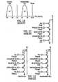
- a single column 40a of EEPROM cellsis illustrated as including a pair of NAND-type strings.
- This pair of NAND-type stringsincludes an upper NAND-type string, which may belong to an upper block of EEPROM cells, which includes multiple pages of cells, and a lower NAND-type string, which may belong to a lower block of EEPROM cells, which includes multiple pages of cells.
- the upper and lower NAND-type stringsare tied to a common source line CSL.
- the upper NAND-type stringincludes an NMOS transistor having a gate terminal connected to an upper string select line SSLU and an NMOS transistor having a gate terminal connected to an upper ground select line GSLU.
- the upper NAND-type stringalso includes a plurality of three-state EEPROM cells. These three-state EEPROM cells have control gates connected to respective word lines, which are associated with a plurality of pages of nonvolatile memory: PAGE 1, PAGE 3, ..., PAGE 39.
- a pair of SLC EEPROM cells associated with PAGES 41 and 43are also provided. These SLC EEPROM cells may be outside the address space of virtual page programming and reading operations.
- the lower NAND-type stringincludes an NMOS transistor having a gate terminal connected to a lower string select line SSLL and an NMOS transistor having a gate terminal connected to a lower ground select line GSLL.
- the lower NAND-type stringalso includes a plurality of three-state EEPROM cells.
- These three-state EEPROM cellshave control gates connected to respective word lines, which are associated with a plurality of pages of nonvolatile memory: PAGE 0, PAGE 2, ..., PAGE 38.
- a pair of SLC EEPROM cells associated with PAGES 40 and 42are also provided.
- the EEPROM cells associated with the pages PAGE 0, PAGE 2, ..., PAGE 38 of a lower block of memory and the EEPROM cells associated with the pages PAGE 1, PAGE 3, ..., PAGE 39 of an upper block of memorymay collectively form a plurality of "virtual" pages of nonvolatile memory.
- FIG. 4Billustrates an EEPROM device 40b according to the invention.
- the EEPROM device 40bincludes a nonvolatile memory array with upper and lower memory blocks, a page buffer and data input/output circuit.
- the EEPROM device 40bis illustrated as an eight column device that supports 2N "physical" pages (e.g., rows) of nonvolatile memory and N "virtual" pages of nonvolatile memory, but only incurs the memory array layout footprint (i.e., area penalty) of a conventional nonvolatile memory supporting 2N pages of SLC EEPROM cells.
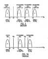
- FIG. 4Cillustrates operations to program a corresponding pair of three-state EEPROM cells in a sequential manner, with the upper cell within the pair being programmed before the lower cell within the pair.
- This program ordermay be reversed.
- the upper cellmay be the EEPROM cell associated with word line WLU ⁇ 0> and bit line BL ⁇ 0> in FIG. 4B and the lower cell may be the EEPROM cell associated with word line WLL ⁇ 0> and bit line BL ⁇ 0> in FIG. 4B .
- the programming of two bits of "physical" data as 1/1does not involve any change in the threshold voltages of the upper and lower cells within the pair.
- the threshold voltages of the upper and lower cells within the pairremain at their original “erased” levels (i.e., Vth ⁇ VR1, where VR1 is a first reference voltage).
- the programming of two bits of "physical" data as 1/0does not involve any change in the threshold voltage of the upper cell, but causes the threshold voltage of the lower cell to be increased to a level between VR1 and VR2.
- the programming of two bits of "physical" data as 0/1causes the threshold voltage of the upper cell to be increased to a level between VR1 and VR2, but does not involve any change in the threshold voltage of the lower cell.
- the programming of two bits of "physical" data as 0/0causes the threshold voltages of the upper and lower cells to be increased to a level between VR1 and VR2, as illustrated.
- the programming and reading operations for the upper cellare independent from that of the lower cell and vice versa.
- FIG. 4Dillustrates operations to program a corresponding pair of three-state EEPROM cells with a third bit of "virtual" data, after the pair has been programmed with two bits of "physical” data in accordance with FIG. 4C .
- These program operationsinclude cases (a) - (h).
- case (a)the "virtual" program operation does not require any change in the threshold voltages of the pair of cells to achieve 3-bit data as 1/1/1.
- case (b)which is a special case (S)
- the "virtual" program operationrequires increasing the threshold voltages of both upper and lower cells in the pair to levels in excess of VR2 (i.e., Vth>VR2, where VR2 is a second reference voltage), to achieve 3-bit data as 1/1/0.
- the "virtual" program operationdoes not require any additional change in the threshold voltages of the pair of cells to achieve 3-bit data as 1/0/1.
- the "virtual" program operationrequires increasing the threshold voltages of the lower cell in the pair to a level in excess of VR2 to achieve 3-bit data as 1/0/0.
- the "virtual" program operationdoes not require any additional change in the threshold voltages of the pair of cells to achieve 3-bit data as 0/1/1.
- the "virtual” program operationrequires increasing the threshold voltage of the upper cell in the pair to a level in excess of VR2 to achieve 3-bit data as 0/1/0.
- the "virtual" program operationdoes not require any additional change in the threshold voltages of the pair of cells to achieve 3-bit data as 0/0/1.
- the "virtual" program operationrequires increasing the threshold voltage of the upper cell in the pair to a level in excess of VR2 to achieve 3-bit data as 0/0/0.
- each virtual page program operationincludes a plurality of read operations from corresponding upper and lower physical pages within a multi-page memory array having upper and lower blocks.
- EEPROM cells in an upper page of the memory arraycan be read using a normal SLC read operation.
- This SLC read operationincludes setting a selected word line in an upper block of the memory array to the first reference voltage VR1.
- This upper page of read datais identified by the reference character A1.
- a corresponding lower page of datacan be read using a normal SLC read operation, Block 104.
- This SLC read operationincludes setting a selected word line in a lower block of the memory array to the first reference voltage VR1.
- This lower page of read datais identified by the reference character A2.
- a virtual page of datareferred to herein as a third page of data A3, is then programmed into a "virtual" page of the memory array by encoding both the upper page of "physical" data A1 and the lower page of "physical” data A2 with this third page of data A3.
- These encoding operationsresult in the generation of "encoded" upper cell data A1* and "encoded” lower cell data A2*.
- FIG. 5Bthese encoding operations are non-destructive, which means that A1 can be decoded directly from A1* and A2 can be decoded directly from A2*.
- the superscript "P" in A1* ⁇ 7:0> and A2* ⁇ 7:0>designates further programming to raise a threshold voltage above VR2 and "S" designates the special case (b) illustrated by FIG. 4D where both lower and upper cells within a pair are further programmed to have threshold voltages in excess of VR2.
- FIG 5Billustrates operations 200 to read "physical" data from selected pages of EEPROM cells.
- This "physical" datacorresponds to BIT 1 and BIT 2 of the three bit data illustrated by FIG. 5A .
- These read operations 200include the performance of a special case read operation from corresponding upper and lower pages of a nonvolatile memory array.
- this special case read operationincludes setting the selected word lines for the upper and lower pages in the upper and lower blocks, respectively, at the second reference voltage VR2 while concurrently setting the unselected word lines at VREAD.
- Block 206a check is then made to determine whether any of the corresponding bit lines, which are connected to the upper and lower blocks, are discharged.
- FIG. 5Cillustrates operations 300 to read "virtual" data from a pair of pages of EEPROM cells.
- the selected and unselected word lines for the upper blockare set to VR2 and VREAD, respectively, to detect whether any of the cells in the selected upper page satisfy the case (b), case (f) or case (h) conditions identified by FIG. 4D .
- the selected and unselected word lines for the lower blockare set to VR2 and VREAD, respectively, to detect whether any of the cells in the selected lower page satisfy the case (b) or case (d) conditions identified by FIG. 4D .
- FIG. 4Dillustrate how embodiments of the invention are relatively immune from multi-bit errors caused in response to threshold voltage programming errors. For example, if the programming state illustrated by case (a) is erroneously reflected as a case (c) or case (e) state upon reading, then the correct 3-bit data value of 1/1/1 will be erroneously reflected upon reading as 1/0/1, which represents a single bit error in A2, or 0/1/1, which reflects a single bit error in A1.
- case (g)is erroneously reflected as a case (c), case (e) or case (h) state upon reading
- the correct 3-bit data value of 0/0/1will be erroneously reflected upon reading as 1 /0/1, which represents a single bit error in A1, or 0/1/1, which reflects a single bit error in A2, or 0/0/0, which reflects a single bit error in A3.
- FIG. 4Dillustrates the programming state illustrated by case (g)
Landscapes
- Engineering & Computer Science (AREA)
- Computer Hardware Design (AREA)
- Microelectronics & Electronic Packaging (AREA)
- Read Only Memory (AREA)
- Semiconductor Memories (AREA)
Description
- The invention relates to a nonvolatile memory device and a method of operating the same. This application claims priority to
Korean Application No. 2005-34825, filed April 27, 2005 - One class of nonvolatile memory devices includes electrically erasable programmable read only memory (EEPROM), which may be used in many applications including embedded applications and mass storage applications. In typical embedded applications, an EEPROM device may be used to provide code storage in personal computers or mobile phones, for example, where fast random access read times may be required. Typical mass storage applications include memory card applications requiring high capacity and low cost. One category of EEPROM devices includes NAND-type flash memories, which can provide a low cost and high capacity alternative to other forms of nonvolatile memory.
FIG. 1A illustrates a conventionalflash memory array 10 having a plurality of NAND-type strings therein. Each of these NAND-type strings includes a plurality of EEPROM cells, which are associated with respective even and odd bit lines BL0_e, BL0_o, ..., BLn_e , BLn_o. These bit lines are connected to apage buffer 12 having a plurality of buffer circuits PB0, ..., PBn therein. Each EEPROM cell includes a floating gate electrode and a control gate electrode, which is electrically connected to a respective word line WL0, WL1, ..., WLn. Access to each NAND string is enabled by driving a string select line SSL to alogic 1 voltage during reading and programming operations. Each NAND string also includes a respective ground select transistor, which is electrically connected to a ground select line GSL. - As illustrated by
FIG. 1 B , the EEPROM cells within theflash memory array 10 ofFIG. 1A may be cells that support a single programmed state. EEPROM cells that support only a single programmed state are typically referred to as single level cells (SLC). In particular, an SLC may support an erased state, which may be treated as alogic 1 storage value, and a programmed state, which may be treated as alogic 0 storage value. The SLC may have a negative threshold voltage Vth when erased (e.g., -3V<Vth<-1V) and a positive threshold voltage when programmed (e.g., 1V<Vth<3V). This programmed state may be achieved by setting the bit line BL to alogic 0 value (e.g., 0 Volts), applying a program voltage Vpgm to a selected EEPROM cell and applying a pass voltage Vpass to the unselected EEPROM cells within a string, as illustrated byFIG. 1C . In addition, during programming the NAND string may be enabled by applying a positive voltage (e.g., power supply voltage Vdd) to the string select line SSL and a ground voltage (e.g., 0 Volts) to the ground select line GSL. - Moreover, the programmed state or erased state of an EEPROM cell may be detected by performing a read operation on a selected cell. As illustrated by
FIG. 1 D , a NAND string will operate to discharge a precharged bit line BL when a selected cell is in an erased state and the selected word line voltage (e.g., 0 Volts) is greater than the threshold voltage of the selected cell. However, when a selected cell is in a programmed state, the corresponding NAND string will provide an open circuit to the precharged bit line BL because the selected word line voltage (e.g., 0 Volts) is less than the threshold voltage of the selected cell and the selected cell remains "off". Other aspects of NAND-type flash memories are disclosed in an article byJung et al., entitled "A 3.3 Volt Single Power Supply 16-Mb Nonvolatile Virtual DRAM Using a NAND Flash Memory Technology", IEEE Journal of Solid-State Circuits, Vol. 32, No. 11, pp. 1748-1757, November (1997). the disclosure of which is hereby incorporated herein by reference. - EEPROM cells that support multiple programmed states are typically referred to as multi-level cells (MLC). As illustrated by
FIG. 2 , an MLC that supports an erased state and three different programmed states operates to store two data bits per cell. These and other aspects of an MLC having two data bits per cell is disclosed in an article byTakeuchi et al., entitled "A Multipage Cell Architecture for HighSpeed Programming Multilevel NAND Flash Memories", IEEE Journal of Solid-State Circuits, Vol. 33, No. 8, pp. 1228-1238, August (1998). Commonly assignedU.S. Patent Nos. 5,862,074 and5,768,188 also disclose aspects of multi-level EEPROM cells arranged in a NAND-type configuration. FIGS. 3A-3B illustrate how a pair of three-state EEPROM cells may support 3-bit programming. InFIG. 3A , an MLC is illustrated as supporting an erased state and two possible programmed states. As will be understood by those skilled in the art, the erased state may be distinguished from the two possible programmed states by applying a first reference voltage VR1 to a control electrode of a selected EEPROM cell during a read operation. This first reference voltage VR1 should be set to a level between the maximum acceptable threshold voltage of an erased cell (shown as VO) and the minimum acceptable threshold voltage of a cell programmed to state 1 (shown as V1). Similarly, the second programmed state (state 2) may be distinguished from the erased and first programmed states by applying a second reference voltage VR2 to a selected EEPROM cell during a read operation. This second reference voltage VR2 should be set to a level between the maximum acceptable threshold voltage of a cell programmed tostate 1 and the minimum acceptable threshold voltage of a cell programmed to state 2 (shown as V2). As illustrated byFIG. 3B , two adjacent three-level EEPROM cells in the same physical row of memory may be programmed into one of eight possible states (111), (110), ..., (001), (000) to support 3-bits of data per cell pair. Additional aspects of three-state EEPROM cells are disclosed in an article byTanaka et al., entitled "A 3.4-Mbyte/sec Programming 3-Level NAND Flash Memory Saving 40% Die Size Per Bit", 1997 Symposium on VLSI Circuits Digest of Technical Papers, Section 9.3, pp. 65-66 (1997). Unfortunately, the use of 3-state EEPROM cells in the pair configuration ofFIG. 3B may require the use of complex error detection and correction circuitry because any single cell failure will typically result in a corresponding 3-bit data error for both cells in the corresponding pair.US 2004/0080979 A1 discloses a non-volatile flash memory device comprising a memory array having a plurality of three-level flash memory cells, that are configured to encode data on the basis of groups of such three-level flash memory cells.- It is the technical problem underlying the invention to provide a non-volatile memory device and a corresponding operating method which are capable to reduce or avoid the inconveniences of the prior art mentioned above.
- The invention achieves this problem by providing a non-volatile semiconductor memory device having the features of
claim 1, and a method of operating a flash memory device having the features of claim 15 or 22. Advantageous embodiments of the invention are mentioned in the subclaims, the wording of which is herewith incorporated into the description by reference to avoid unnecessary text repetition. - Advantageous embodiments of the invention are described below and shown in the drawings which also show the conventional embodiments explained above to facilitate the understanding of the invention. In the drawings:
FIG. 1A is an electrical schematic of a conventional nonvolatile memory device having NAND-type strings of EEPROM cells therein,FIG. 1 B is a graph illustrating the relative threshold voltages of an erased and programmed EEPROM cell, according to the prior art,FIG. 1C is an electrical schematic of a NAND-type string of EEPROM cells showing programming bias conditions,FIG. 1 D illustrates current flow in a NAND-type string during operations to read data from an erased EEPROM cell and a programmed EEPROM cell according to the prior art,FIG. 2 is a graph illustrating the relative threshold voltages of a four-state EEPROM cell according to the prior art,FIG. 3A is a graph illustrating the relative threshold voltages of a three-state EEPROM cell according to the prior art,FIG. 3B illustrates the threshold voltage distributions of two adjacent three-state EEPROM cells that support 3-bit data when paired together in the same row of memory,FIG. 4A is an electrical schematic of upper and lower NAND-type strings of EEPROM cells that support virtual page programming according to the invention,FIG. 4B is an electrical schematic of a NAND-type EEPROM device according to of the invention,FIG. 4C is a diagram that illustrates operations to program three-state EEPROM cells, according to the invention,FIG. 4D is a diagram that illustrates operations to program three-state EEPROM cells, according to the invention,FIG. 4E is a flow diagram that illustrates operations to program "virtual" pages of EEPROM cells, according to of the invention,FIG. 5A illustrates operations to program a virtual EEPROM cell, according to the invention,FIG. 5B is a flow diagram illustrating operations to read data from three-state EEPROM cells, according to the present invention, andFIG. 5C is a flow diagram illustrating operations to read data from three-state EEPROM cells, according to the present invention.- The invention now will be described more fully herein with reference to the accompanying drawings, in which preferred embodiments of the invention are shown. Like reference numerals refer to like elements throughout and signal lines and signals thereon may be referred to by the same reference characters. Signals may also be synchronized and/or undergo minor boolean operations (e.g., inversion) without being considered different signals.
- Referring now to
FIG. 4A , asingle column 40a of EEPROM cells is illustrated as including a pair of NAND-type strings. This pair of NAND-type strings includes an upper NAND-type string, which may belong to an upper block of EEPROM cells, which includes multiple pages of cells, and a lower NAND-type string, which may belong to a lower block of EEPROM cells, which includes multiple pages of cells. The upper and lower NAND-type strings are tied to a common source line CSL. The upper NAND-type string includes an NMOS transistor having a gate terminal connected to an upper string select line SSLU and an NMOS transistor having a gate terminal connected to an upper ground select line GSLU. The upper NAND-type string also includes a plurality of three-state EEPROM cells. These three-state EEPROM cells have control gates connected to respective word lines, which are associated with a plurality of pages of nonvolatile memory:PAGE 1,PAGE 3, ...,PAGE 39. A pair of SLC EEPROM cells associated withPAGES PAGE 0,PAGE 2, ...,PAGE 38. A pair of SLC EEPROM cells associated withPAGES FIGS. 4B-4E and5A-5C , the EEPROM cells associated with thepages PAGE 0,PAGE 2, ...,PAGE 38 of a lower block of memory and the EEPROM cells associated with thepages PAGE 1,PAGE 3, ...,PAGE 39 of an upper block of memory may collectively form a plurality of "virtual" pages of nonvolatile memory. These "virtual" pages are illustrated as VPAGE44,VPAGE 45, ..., VPAGE63. Accordingly, thecolumn 40a of EEPROM cells is illustrated as supporting one column of a 64 page nonvolatile memory. Embodiments of the present invention are not limited to any particular capacity of memory, page width or NAND string length. FIG. 4B illustrates anEEPROM device 40b according to the invention. TheEEPROM device 40b includes a nonvolatile memory array with upper and lower memory blocks, a page buffer and data input/output circuit. In particular, theEEPROM device 40b is illustrated as an eight column device that supports 2N "physical" pages (e.g., rows) of nonvolatile memory and N "virtual" pages of nonvolatile memory, but only incurs the memory array layout footprint (i.e., area penalty) of a conventional nonvolatile memory supporting 2N pages of SLC EEPROM cells.FIG. 4C illustrates operations to program a corresponding pair of three-state EEPROM cells in a sequential manner, with the upper cell within the pair being programmed before the lower cell within the pair. This program order may be reversed. For purposes of illustration herein, the upper cell may be the EEPROM cell associated with word line WLU<0> and bit line BL<0> inFIG. 4B and the lower cell may be the EEPROM cell associated with word line WLL<0> and bit line BL<0> inFIG. 4B . As illustrated byFIG. 4C , the programming of two bits of "physical" data as 1/1 does not involve any change in the threshold voltages of the upper and lower cells within the pair. Thus, the threshold voltages of the upper and lower cells within the pair remain at their original "erased" levels (i.e., Vth<VR1, where VR1 is a first reference voltage). The programming of two bits of "physical" data as 1/0 does not involve any change in the threshold voltage of the upper cell, but causes the threshold voltage of the lower cell to be increased to a level between VR1 and VR2. Similarly, the programming of two bits of "physical" data as 0/1 causes the threshold voltage of the upper cell to be increased to a level between VR1 and VR2, but does not involve any change in the threshold voltage of the lower cell. Finally, the programming of two bits of "physical" data as 0/0 causes the threshold voltages of the upper and lower cells to be increased to a level between VR1 and VR2, as illustrated. The programming and reading operations for the upper cell are independent from that of the lower cell and vice versa.FIG. 4D illustrates operations to program a corresponding pair of three-state EEPROM cells with a third bit of "virtual" data, after the pair has been programmed with two bits of "physical" data in accordance withFIG. 4C . These program operations include cases (a) - (h). In case (a), the "virtual" program operation does not require any change in the threshold voltages of the pair of cells to achieve 3-bit data as 1/1/1. In case (b), which is a special case (S), the "virtual" program operation requires increasing the threshold voltages of both upper and lower cells in the pair to levels in excess of VR2 (i.e., Vth>VR2, where VR2 is a second reference voltage), to achieve 3-bit data as 1/1/0. In case (c), the "virtual" program operation does not require any additional change in the threshold voltages of the pair of cells to achieve 3-bit data as 1/0/1. In case (d), the "virtual" program operation requires increasing the threshold voltages of the lower cell in the pair to a level in excess of VR2 to achieve 3-bit data as 1/0/0. In case (e), the "virtual" program operation does not require any additional change in the threshold voltages of the pair of cells to achieve 3-bit data as 0/1/1. In case (f), the "virtual" program operation requires increasing the threshold voltage of the upper cell in the pair to a level in excess of VR2 to achieve 3-bit data as 0/1/0. In case (g), the "virtual" program operation does not require any additional change in the threshold voltages of the pair of cells to achieve 3-bit data as 0/0/1. Finally, in case (h), the "virtual" program operation requires increasing the threshold voltage of the upper cell in the pair to a level in excess of VR2 to achieve 3-bit data as 0/0/0.- In particular, each virtual page program operation includes a plurality of read operations from corresponding upper and lower physical pages within a multi-page memory array having upper and lower blocks. As illustrated by
Block 102, EEPROM cells in an upper page of the memory array can be read using a normal SLC read operation. This SLC read operation includes setting a selected word line in an upper block of the memory array to the first reference voltage VR1. This upper page of read data is identified by the reference character A1. Thereafter, a corresponding lower page of data can be read using a normal SLC read operation,Block 104. This SLC read operation includes setting a selected word line in a lower block of the memory array to the first reference voltage VR1. This lower page of read data is identified by the reference character A2. - A virtual page of data, referred to herein as a third page of data A3, is then programmed into a "virtual" page of the memory array by encoding both the upper page of "physical" data A1 and the lower page of "physical" data A2 with this third page of data A3. These encoding operations result in the generation of "encoded" upper cell data A1* and "encoded" lower cell data A2*. As illustrated by
FIG. 5B , these encoding operations are non-destructive, which means that A1 can be decoded directly from A1* and A2 can be decoded directly from A2*. These encoding operations may be illustrated more fully by reference toFIGS. 4D and5A , for an example case where a first page of data, A1 <7:0>, equals <10110001>, a second page of data, A2<7:0>, equals <01110110> and a third page of data, A3<7:0>, equals <10001010>:
A1<7:0> = <10110001>;
A2<7;0> = <01110110>; and
A3<7:0> = <10001010>
(ENCODE)
A1*<7:0> = <10PSS00 P01>; and
A2*<7:0> =< 01SS0110P>.
In this example, the superscript "P" in A1* <7:0> and A2*<7:0> designates further programming to raise a threshold voltage above VR2 and "S" designates the special case (b) illustrated byFIG. 4D where both lower and upper cells within a pair are further programmed to have threshold voltages in excess of VR2. Thus, among other things, the above example illustrates that one pair of EEPROM cells in column six (6) of theEEPROM device 40b is programmed to support 3-bits of data as 0/1/0 (i.e., A1 <6>=0, A2<6>=1 and A3<6>=0), which corresponds to case (f) inFIG. 4D . Another pair of EEPROM cells in column zero (0) of theEEPROM device 40b is programmed to support 3-bits of data as 1/0/0 (i.e., A1<0>=1, A2<0>=0 and A3<0>=0), which corresponds to case (d) inFIG. 4D . - Referring again to
FIG. 4E and alsoFIG. 5A , once the encoded data A1* and A2* is generated in response to reading from the upper and lower pages of data A1 and A2, Blocks 102-104, the corresponding upper page of EEPROM cells associated with A1 is programmed with the encoded data A1* and then verified at the second reference voltage VR2,Blocks Blocks FIG 5B illustratesoperations 200 to read "physical" data from selected pages of EEPROM cells. This "physical" data corresponds toBIT 1 andBIT 2 of the three bit data illustrated byFIG. 5A . These readoperations 200 include the performance of a special case read operation from corresponding upper and lower pages of a nonvolatile memory array. As illustrated byBlocks Block 206, a check is then made to determine whether any of the corresponding bit lines, which are connected to the upper and lower blocks, are discharged. If this check results in a negative answer, which means the special case is present (i.e., BIT1/BIT2/ BIT3=1/1/0), then the read data for the corresponding physical cell equals alogic 1 value,Block 210. However, if the check results in a positive answer, then a normal SLC read is performed on the selected cell with the selected word line set to the first reference voltage VR1,Block 208. The read data for a selected physical page is then output from a page buffer,Block 212. Thus, for the above example, a special case read of the selected upper page (programmed with A1*<7:0>=<10PSS00 P01> would result in the following first bit line condition: BL1<7:0>=<00110000>, which indicates that A1<5:4>=<11 >, Block 202-204. In contrast, a normal SLC read of the selected upper page (programmed with A1*<7:0>=<10110001>) would result in the following second bit line condition: BL2<7:0>=<01111110>,Block 208. These first and second bit line conditions (BL1<7:0>=<00110000> and BL2<7:0>=<01111110>) are combined within the page buffer to thereby generate the value of A1<7:0> as <10110001>,Block 212. This value of A1 is generated by inverting every bit associated with the second bit line condition, subject to the constraint set by the first bit line condition, which requires that A1 <5:4>=<11 > because of the presence of special case programming.FIG. 5C illustratesoperations 300 to read "virtual" data from a pair of pages of EEPROM cells. AtBlocks FIG. 4D . Thus, for the above example (programmed with A1*<7:0>=<10PSS00 P01>), this read operation would result in the following third bit line condition: BL3<7:0>=<01110100>, which is stored in a first latch within the page buffer,Block 306. Thereafter, atBlocks FIG. 4D . Thus, for the above example (programmed with A2*<7:0>=<01 SS0110P>), this read operation would result in the following fourth bit line condition: BL4<7:0>=<00110001 >, which is stored in a second latch within the page buffer,Block 312.- At
Block 314, the data with the first and second latches is compared on a bit-by-bit basis:
BL3<7:0>=<01110100>;
BL4<7:0>=<00110001>.
Because only BL3<5:4> = BL4<5:4> = <11>, A3<5:4>=<00>,Block 316. AtBlock 318, a NOR operation is performed on the remaining bits to yield A3<7:6;3:0>=<10;1010>. The data is then output from the page buffer,Block 320. In other embodiments of the present invention, the page buffer may perform alternative operations to resolve the above-described read operations. - The above-described programming operations illustrated by
FIG. 4D illustrate how embodiments of the invention are relatively immune from multi-bit errors caused in response to threshold voltage programming errors. For example, if the programming state illustrated by case (a) is erroneously reflected as a case (c) or case (e) state upon reading, then the correct 3-bit data value of 1/1/1 will be erroneously reflected upon reading as 1/0/1, which represents a single bit error in A2, or 0/1/1, which reflects a single bit error in A1. Likewise, if the programming state illustrated by case (g), for example, is erroneously reflected as a case (c), case (e) or case (h) state upon reading, then the correct 3-bit data value of 0/0/1 will be erroneously reflected upon reading as 1 /0/1, which represents a single bit error in A1, or 0/1/1, which reflects a single bit error in A2, or 0/0/0, which reflects a single bit error in A3. The same is true for other programming states illustrated byFIG. 4D .
Claims (24)
- A nonvolatile memory device, comprising one of- a memory array (40B, 40A) having at least first (PAGE1,..., PAGE39) and second (PAGE0, ..., PAGE38) blocks of three-state non-volatile memory cells therein that are configured to individually support first and second blocks of data, respectively, and further configured to collectively support a third block (VPAGE44,..., VPAGE63) of data encoded onto the first and second blocks of data, or- a NAND-type flash memory array (40B,40A) having at least first (PAGE1, PAGE3,...) and (PAGE0, PAGE2,...) second N-page blocks of EEPROM cells therein that are configured to operate individually each as an N-page physical block of EEPROM cells and collectively as an N-page virtual block (VPAGE44, VPAGE45,...) of EEPROM cells.
- The nonvolatile memory device of Claim 1, wherein said memory array is configured so that programming of the third block of data or of the virtual memory cell is verified at only a single reference voltage for all values of data contained in the third block of data or in the virtual memory cell.
- The nonvolatile memory device of Claim 1 or 2, wherein said memory array is a flash memory array configured so that reading of the virtual memory cell occurs by evaluating whether any of the physical memory cells associated with the virtual memory cell are programmed to a threshold voltage in excess of the single reference voltage.
- The nonvolatile memory device of any of claims 1 to 3, wherein the memory array is a flash memory array which comprises first and second memory strings or blocks of three-state memory cells that are configured to operate individually as first and second blocks of physical memory cells, respectively, and collectively as a block of virtual memory cells.
- The nonvolatile memory device of Claim 4, wherein the memory cell array comprises a plurality of memory blocks, with each memory block comprising a plurality of memory strings and a plurality of bit lines, each of which is connected to a first memory string and a second memory string, wherein the first memory strings and the second memory strings of three-state memory cells operate individually as first and second page blocks, respectively, and collectively as a third page block of virtual memory cells.
- The nonvolatile memory device of Claim 4 or 5, wherein said first block of memory cells comprises a plurality of NAND strings of EEPROM cells.
- The nonvolatile memory device of Claim 6, wherein each of the plurality of NAND strings of EEPROM cells includes at least one SLC EEPROM cell.
- The nonvolatile memory device of any of claims 1 to 7, wherein the memory cell array comprises a plurality of memory strings in which electrically erasable and programmable memory cells are serially connected, each of said memory strings have at least one odd-state memory cell storing therein an odd number of threshold voltage states;
a plurality of bit lines is provided which are electrically connected to the strings; and
a plurality of word lines is provided which are connected to respective cells in strings wherein reading and programming a bit of data from the odd-state cells is performed by enabling more than one word line to be selected or by activating a bit line. - The nonvolatile semiconductor memory device of Claim 8, wherein the at least one odd-state memory cell is a three-state cell.
- The nonvolatile semiconductor memory device of Claim 8 or 9, wherein the odd-state memory cells are operated in the unit of two cells.
- The nonvolatile semiconductor memory device of Claim 9 or 10, wherein the memory cell string comprises eleven three-state cells and a two-state cell.
- The nonvolatile semiconductor memory device of Claim 11, wherein the twostate cell is connected to one end of strings near the bit line.
- The nonvolatile semiconductor memory device of Claim 9 or 10, wherein the memory cell string comprises twenty two three-state cells and two two-state cells.
- The nonvolatile semiconductor memory device of Claim 13, wherein at least one of the two-state cells is connected in one end of strings near the bit line.
- A method of operating a flash memory device which comprises a NAND-type flash memory array having at least first and second N-page blocks of EEPROM cells therein that are configured to operate individually each as an N-page physical block of EEPROM cells and collectively as an N-page virtual block of EEPROM cells, comprising the steps of:- operating the at least first and second N-page blocks individually as N-page physical blocks of EEPROM cells and collectively as an N-page virtual block of EEPROM cells, and- programming the NAND-type EEPROM array with a third page of data for said virtual block by reading a first page of data from a first page of data of the first block and a second page of data from a corresponding first page of data of the second block, and then overwriting the first and second pages of data with modified data that encodes three the first, second and third page of data therein.
- The method of Claim 15, wherein said programming step is followed by the step of reading three pages of data from the two pages of EEPROM cells within the NAND-type EEPROM array.
- The method of Claim 16, wherein the EEPROM cells are three-state EEPROM cells.
- The method of any of claims 15 to 17, further comprising the steps of:encoding a third page of flash memory data into first and second pages of flash memory data to thereby generate first and second pages of encoded flash memory data;programming a first page of flash memory cells in the flash memory device with the first page of encoded flash memory data;programming a second page of flash memory cells in the flash memory device with the second page of encoded flash memory data; andgenerating the third page of flash memory data in response reading the first and second pages of encoded flash memory data from the first and second pages of flash memory cells, respectively.
- The method of Claim 18, wherein said encoding step is preceded by the steps of reading the first and second pages of flash memory data from the first and second pages of flash memory cells, respectively.
- The method of Claim 18 or 19, wherein said step of programming the first page of flash memory cells with the first page of encoded flash memory data is followed by the step of generating the first page of flash memory data in response to reading the first page of encoded flash memory data from the first page of flash memory cells.
- The method of any of Claims 18 to 20, wherein said step of programming the second page of flash memory cells with the second page of encoded flash memory data is followed by the step of generating the second page of flash memory data in response to reading the second page of encoded flash memory data from the second page of flash memory cells.
- A method of operating a flash memory device which comprises a NAND-type flash memory array having at least first and second N-page blocks of EEPROM cells therein that are configured to operate individually each as an N-page physical blocks of EEPROM cells and collectively as an N-page virtual block of EEPROM cells, comprising the following steps:- reading a first page of data from a first page of EEPROM cells from the first block- reading a second page of data from a corresponding first page of EEPROM cells from the second block; and- reading a third page of data from the virtual block by reading the first and second pages of data from the first and second blocks respectively, into a page buffer and decoding the first and second pages of data in the page buffer into the third page of data.
- The method of Claim 22, wherein the first and second pages of EEPROM cells are in different multi-page blocks of EEPROM cells.
- The method of Claim 22 or 23, wherein the third page of data is read before reading the first page of data or the second page of data.
Applications Claiming Priority (1)
| Application Number | Priority Date | Filing Date | Title |
|---|---|---|---|
| KR1020050034825AKR100666174B1 (en) | 2005-04-27 | 2005-04-27 | 3-level nonvolatile semiconductor memory device and driving method thereof |
Publications (2)
| Publication Number | Publication Date |
|---|---|
| EP1720168A1 EP1720168A1 (en) | 2006-11-08 |
| EP1720168B1true EP1720168B1 (en) | 2008-04-30 |
Family
ID=36791826
Family Applications (1)
| Application Number | Title | Priority Date | Filing Date |
|---|---|---|---|
| EP06004699AActiveEP1720168B1 (en) | 2005-04-27 | 2006-03-08 | Integrated circuit device, flash memory array, nonvolatile memory device and operating method |
Country Status (7)
| Country | Link |
|---|---|
| US (3) | US7388778B2 (en) |
| EP (1) | EP1720168B1 (en) |
| JP (1) | JP4970834B2 (en) |
| KR (1) | KR100666174B1 (en) |
| CN (2) | CN101807432B (en) |
| DE (1) | DE602006001026T2 (en) |
| TW (1) | TWI310189B (en) |
Families Citing this family (63)
| Publication number | Priority date | Publication date | Assignee | Title |
|---|---|---|---|---|
| KR100666185B1 (en)* | 2005-07-29 | 2007-01-09 | 삼성전자주식회사 | 3-level nonvolatile semiconductor memory device and driving method thereof |
| KR100666183B1 (en)* | 2006-02-01 | 2007-01-09 | 삼성전자주식회사 | 3-level nonvolatile semiconductor memory device and driving method thereof |
| KR100666223B1 (en)* | 2006-02-22 | 2007-01-09 | 삼성전자주식회사 | 3-level nonvolatile semiconductor memory device for reducing coupling noise between memory cells and driving method thereof |
| US7336532B2 (en)* | 2006-05-12 | 2008-02-26 | Elite Semiconductor Memory | Method for reading NAND memory device and memory cell array thereof |
| US7366017B2 (en) | 2006-08-22 | 2008-04-29 | Micron Technology, Inc. | Method for modifying data more than once in a multi-level cell memory location within a memory array |
| KR100871694B1 (en)* | 2006-10-04 | 2008-12-08 | 삼성전자주식회사 | Program method and data read method of non-volatile memory device using six threshold voltage levels, and non-volatile memory device using the same |
| KR100806119B1 (en)* | 2006-10-23 | 2008-02-22 | 삼성전자주식회사 | Flash memory device and multi-page program method of flash memory device |
| US7848141B2 (en)* | 2006-10-31 | 2010-12-07 | Hynix Semiconductor Inc. | Multi-level cell copyback program method in a non-volatile memory device |
| ITVA20060065A1 (en)* | 2006-11-03 | 2008-05-04 | St Microelectronics Srl | MEMORY WITH THREE-LEVEL CELLS AND ITS MANAGEMENT METHOD. |
| KR100855972B1 (en)* | 2007-01-23 | 2008-09-02 | 삼성전자주식회사 | A nonvolatile memory system having a plurality of memory cell arrays having different read latency and a data read method of the nonvolatile memory system |
| JP2009015978A (en) | 2007-07-05 | 2009-01-22 | Toshiba Corp | Semiconductor memory device and memory system |
| US7489543B1 (en)* | 2007-07-25 | 2009-02-10 | Micron Technology, Inc. | Programming multilevel cell memory arrays |
| KR100938044B1 (en)* | 2007-09-10 | 2010-01-21 | 주식회사 하이닉스반도체 | Nonvolatile memory device and multilevel cell program method thereof |
| US7639532B2 (en)* | 2007-10-10 | 2009-12-29 | Micron Technology, Inc. | Non-equal threshold voltage ranges in MLC NAND |
| KR100923820B1 (en) | 2007-10-12 | 2009-10-27 | 주식회사 하이닉스반도체 | Page buffer, memory device having same and operation method thereof |
| KR101391881B1 (en)* | 2007-10-23 | 2014-05-07 | 삼성전자주식회사 | Multi-bit flash memory device and program and read methods thereof |
| KR101426845B1 (en)* | 2007-12-05 | 2014-08-14 | 삼성전자주식회사 | A nonvolatile memory device comprising a common source |
| KR101434401B1 (en)* | 2007-12-17 | 2014-08-27 | 삼성전자주식회사 | Integrated circuit memory device |
| KR101378365B1 (en) | 2008-03-12 | 2014-03-28 | 삼성전자주식회사 | Apparatus and method for hybrid detecting memory data |
| KR101414494B1 (en)* | 2008-03-17 | 2014-07-04 | 삼성전자주식회사 | How to read memory devices and memory data |
| US7920430B2 (en)* | 2008-07-01 | 2011-04-05 | Qimonda Ag | Integrated circuits and methods for operating the same using a plurality of buffer circuits in an access operation |
| KR100965074B1 (en)* | 2008-08-19 | 2010-06-21 | 주식회사 하이닉스반도체 | Nonvolatile Memory Device Memory Cell Block and Additional Information Management Method |
| JP2010092559A (en)* | 2008-10-10 | 2010-04-22 | Toshiba Corp | Nand type flash memory |
| KR101506336B1 (en)* | 2008-10-10 | 2015-03-27 | 삼성전자주식회사 | Nonvolatile memory device having oxide film recovery function and its block management method |
| EP2267724A1 (en)* | 2009-06-26 | 2010-12-29 | STMicroelectronics Rousset SAS | EEPROM memory architecture optimised for embedded memories |
| US9076527B2 (en) | 2009-07-16 | 2015-07-07 | Mikamonu Group Ltd. | Charge sharing in a TCAM array |
| US8238173B2 (en)* | 2009-07-16 | 2012-08-07 | Zikbit Ltd | Using storage cells to perform computation |
| CN101989461B (en)* | 2009-08-06 | 2014-04-02 | 中芯国际集成电路制造(上海)有限公司 | Semiconductor nitride read only memory (NROM) storing device |
| US8417877B2 (en) | 2010-08-31 | 2013-04-09 | Micron Technology, Inc | Stripe-based non-volatile multilevel memory operation |
| US8860117B2 (en) | 2011-04-28 | 2014-10-14 | Micron Technology, Inc. | Semiconductor apparatus with multiple tiers of memory cells with peripheral transistors, and methods |
| CN103176910B (en)* | 2011-12-26 | 2015-10-14 | 群联电子股份有限公司 | Data combination method, controller and storage device for non-volatile memory |
| US8976594B2 (en) | 2012-05-15 | 2015-03-10 | Micron Technology, Inc. | Memory read apparatus and methods |
| US9064551B2 (en) | 2012-05-15 | 2015-06-23 | Micron Technology, Inc. | Apparatuses and methods for coupling load current to a common source |
| US8964474B2 (en) | 2012-06-15 | 2015-02-24 | Micron Technology, Inc. | Architecture for 3-D NAND memory |
| CN103578532B (en)* | 2012-08-01 | 2016-08-10 | 旺宏电子股份有限公司 | Operation method of storage device, memory array and operation method thereof |
| US8811084B2 (en)* | 2012-08-30 | 2014-08-19 | Micron Technology, Inc. | Memory array with power-efficient read architecture |
| US8792279B2 (en) | 2012-11-09 | 2014-07-29 | Sandisk Technologies Inc. | Architectures for data analytics using computational NAND memory |
| US8780635B2 (en) | 2012-11-09 | 2014-07-15 | Sandisk Technologies Inc. | Use of bloom filter and improved program algorithm for increased data protection in CAM NAND memory |
| US8817541B2 (en) | 2012-11-09 | 2014-08-26 | Sandisk Technologies Inc. | Data search using bloom filters and NAND based content addressable memory |
| US8811085B2 (en) | 2012-11-09 | 2014-08-19 | Sandisk Technologies Inc. | On-device data analytics using NAND flash based intelligent memory |
| WO2014074496A2 (en)* | 2012-11-09 | 2014-05-15 | Sandisk Technologies Inc. | Cam nand with or function and full chip search capability |
| US8780632B2 (en) | 2012-11-09 | 2014-07-15 | Sandisk Technologies Inc. | De-duplication techniques using NAND flash based content addressable memory |
| US8780634B2 (en) | 2012-11-09 | 2014-07-15 | Sandisk Technologies Inc. | CAM NAND with OR function and full chip search capability |
| US8780633B2 (en) | 2012-11-09 | 2014-07-15 | SanDisk Technologies, Inc. | De-duplication system using NAND flash based content addressable memory |
| US10127150B2 (en) | 2012-11-09 | 2018-11-13 | Sandisk Technologies Llc | Key value addressed storage drive using NAND flash based content addressable memory |
| US8773909B2 (en) | 2012-11-09 | 2014-07-08 | Sandisk Technologies Inc. | CAM NAND with or function and full chip search capability |
| US9064577B2 (en) | 2012-12-06 | 2015-06-23 | Micron Technology, Inc. | Apparatuses and methods to control body potential in memory operations |
| US9032271B2 (en)* | 2012-12-07 | 2015-05-12 | Western Digital Technologies, Inc. | System and method for lower page data recovery in a solid state drive |
| CN103971750B (en)* | 2013-01-29 | 2017-02-08 | 中国航空工业集团公司西安飞机设计研究所 | Sensitive fault detection method of 9 adjacent units of RAM |
| US8717827B1 (en)* | 2013-02-22 | 2014-05-06 | Hyperstone Gmbh | Method for the permanently reliable programming of multilevel cells in flash memories |
| US9075424B2 (en) | 2013-03-06 | 2015-07-07 | Sandisk Technologies Inc. | Compensation scheme to improve the stability of the operational amplifiers |
| US8995188B2 (en)* | 2013-04-17 | 2015-03-31 | Micron Technology, Inc. | Sharing support circuitry in a memory |
| KR102320830B1 (en)* | 2015-09-24 | 2021-11-03 | 에스케이하이닉스 주식회사 | Semiconductor memory device including three-dimensional array structure |
| US9679650B1 (en) | 2016-05-06 | 2017-06-13 | Micron Technology, Inc. | 3D NAND memory Z-decoder |
| US10176880B1 (en) | 2017-07-01 | 2019-01-08 | Intel Corporation | Selective body reset operation for three dimensional (3D) NAND memory |
| KR20190102596A (en)* | 2018-02-26 | 2019-09-04 | 에스케이하이닉스 주식회사 | Semiconductor memory device and methode for operating thereof |
| US11011239B2 (en)* | 2018-12-27 | 2021-05-18 | Kioxia Corporation | Semiconductor memory |
| KR20200136747A (en)* | 2019-05-28 | 2020-12-08 | 에스케이하이닉스 주식회사 | Memory device, memory system including the memory device and operating method of the memory system |
| KR102743222B1 (en) | 2019-06-12 | 2024-12-17 | 삼성전자 주식회사 | Electronic device and method of utilizing storage space thereof |
| US12027209B2 (en)* | 2019-06-17 | 2024-07-02 | SK Hynix Inc. | Memory device and method of operating the same |
| US11450381B2 (en) | 2019-08-21 | 2022-09-20 | Micron Technology, Inc. | Multi-deck memory device including buffer circuitry under array |
| JP2021128810A (en) | 2020-02-13 | 2021-09-02 | キオクシア株式会社 | Semiconductor storage media and memory systems |
| US11133062B1 (en)* | 2020-05-07 | 2021-09-28 | Micron Technology, Inc. | Two memory cells sensed to determine one data value |
Family Cites Families (56)
| Publication number | Priority date | Publication date | Assignee | Title |
|---|---|---|---|---|
| JPS6342099A (en)* | 1986-08-06 | 1988-02-23 | Fujitsu Ltd | Ternary level rom |
| JPH07120720B2 (en)* | 1987-12-17 | 1995-12-20 | 三菱電機株式会社 | Nonvolatile semiconductor memory device |
| JPH0730000A (en)* | 1993-07-09 | 1995-01-31 | Toshiba Corp | Nonvolatile semiconductor memory device and manufacturing method thereof |
| JPH0766304A (en)* | 1993-08-31 | 1995-03-10 | Toshiba Corp | Semiconductor memory device |
| KR0169267B1 (en) | 1993-09-21 | 1999-02-01 | 사토 후미오 | Nonvolatile Semiconductor Memory |
| JP3476952B2 (en)* | 1994-03-15 | 2003-12-10 | 株式会社東芝 | Nonvolatile semiconductor memory device |
| EP0763242B1 (en)* | 1994-06-02 | 2001-07-11 | Intel Corporation | Sensing schemes for flash memory with multilevel cells |
| KR0169412B1 (en) | 1995-10-16 | 1999-02-01 | 김광호 | Non-volatile semiconductor memory device |
| KR100253868B1 (en)* | 1995-11-13 | 2000-05-01 | 니시무로 타이죠 | Non-volatile semiconductor memory device |
| KR0170707B1 (en) | 1995-11-29 | 1999-03-30 | 김광호 | Non-volatile memory device and its driving method |
| KR0172408B1 (en) | 1995-12-11 | 1999-03-30 | 김광호 | Non-volatile semiconductor memory and method driving the same |
| KR0170714B1 (en) | 1995-12-20 | 1999-03-30 | 김광호 | NAND flash memory device and its driving method |
| JP2870478B2 (en) | 1996-04-25 | 1999-03-17 | 日本電気株式会社 | Nonvolatile semiconductor memory device and method of operating the same |
| DE19631169C2 (en)* | 1996-08-01 | 1998-07-23 | Siemens Ag | Matrix memory in virtual ground architecture |
| KR100204342B1 (en) | 1996-08-13 | 1999-06-15 | 윤종용 | Nonvolatile Semiconductor Memory Devices |
| US5862074A (en) | 1996-10-04 | 1999-01-19 | Samsung Electronics Co., Ltd. | Integrated circuit memory devices having reconfigurable nonvolatile multi-bit memory cells therein and methods of operating same |
| KR100205006B1 (en) | 1996-10-08 | 1999-06-15 | 윤종용 | Semiconductor memory device with automatic defect block mapping function |
| KR100257868B1 (en) | 1997-12-29 | 2000-06-01 | 윤종용 | Erasing method of a nor type flash memory device |
| KR100258574B1 (en) | 1997-12-30 | 2000-06-15 | 윤종용 | Semiconductor memory device and its program/erase verifying method |
| DE19815874C2 (en) | 1998-04-08 | 2002-06-13 | Infineon Technologies Ag | ROM semiconductor memory device with implantation areas for setting a contact resistance and method for its production |
| US5973958A (en)* | 1998-06-23 | 1999-10-26 | Advanced Micro Devices, Inc. | Interlaced storage and sense technique for flash multi-level devices |
| KR100290283B1 (en) | 1998-10-30 | 2001-05-15 | 윤종용 | Nonvolatile semiconductor memory device and word line driving method thereof |
| GB9903490D0 (en)* | 1999-02-17 | 1999-04-07 | Memory Corp Plc | Memory system |
| JP2001093288A (en)* | 1999-09-20 | 2001-04-06 | Toshiba Corp | Nonvolatile semiconductor memory device |
| JP3555076B2 (en) | 1999-12-28 | 2004-08-18 | Necエレクトロニクス株式会社 | Readout circuit of multi-value storage semiconductor storage device |
| US6772274B1 (en)* | 2000-09-13 | 2004-08-03 | Lexar Media, Inc. | Flash memory system and method implementing LBA to PBA correlation within flash memory array |
| US6233175B1 (en)* | 2000-10-21 | 2001-05-15 | Advanced Micro Devices, Inc. | Self-limiting multi-level programming states |
| KR100407572B1 (en) | 2001-01-10 | 2003-12-01 | 삼성전자주식회사 | Method for optimizing distribution profile of cell threshold voltages in a nand-type flash memory device |
| US6587372B2 (en)* | 2001-01-11 | 2003-07-01 | Micron Technology, Inc. | Memory device with multi-level storage cells and apparatuses, systems and methods including same |
| JP3472271B2 (en)* | 2001-02-13 | 2003-12-02 | 株式会社東芝 | Nonvolatile semiconductor memory device |
| US6549483B2 (en) | 2001-03-30 | 2003-04-15 | Atmos Corporation | RAM having dynamically switchable access modes |
| FR2828029B1 (en)* | 2001-07-25 | 2003-09-26 | Centre Nat Rech Scient | ENERGY CONVERSION DEVICE |
| US7554842B2 (en) | 2001-09-17 | 2009-06-30 | Sandisk Corporation | Multi-purpose non-volatile memory card |
| GB0123416D0 (en)* | 2001-09-28 | 2001-11-21 | Memquest Ltd | Non-volatile memory control |
| KR100463197B1 (en) | 2001-12-24 | 2004-12-23 | 삼성전자주식회사 | Nand-type flash memory device with multi-page program, multi-page read, and multi-block erase operations |
| KR100437461B1 (en) | 2002-01-12 | 2004-06-23 | 삼성전자주식회사 | Nand-type flash memory device and erase, program, and copy-back program methods thereof |
| US6549457B1 (en) | 2002-02-15 | 2003-04-15 | Intel Corporation | Using multiple status bits per cell for handling power failures during write operations |
| JP4259922B2 (en) | 2002-07-30 | 2009-04-30 | シャープ株式会社 | Semiconductor memory device |
| US6986016B2 (en)* | 2002-09-30 | 2006-01-10 | International Business Machines Corporation | Contiguous physical memory allocation |
| US6847550B2 (en) | 2002-10-25 | 2005-01-25 | Nexflash Technologies, Inc. | Nonvolatile semiconductor memory having three-level memory cells and program and read mapping circuits therefor |
| KR100496866B1 (en) | 2002-12-05 | 2005-06-22 | 삼성전자주식회사 | Flash memory device having uniform threshold voltage distribution without under-programed or over-programed flash cells and program verify method thereof |
| US7085909B2 (en)* | 2003-04-29 | 2006-08-01 | International Business Machines Corporation | Method, system and computer program product for implementing copy-on-write of a file |
| KR100505705B1 (en) | 2003-08-22 | 2005-08-03 | 삼성전자주식회사 | Program voltage generation circuit for safe programming of flash memory cell and programming method of flash memory cell |
| JP2005092923A (en)* | 2003-09-12 | 2005-04-07 | Renesas Technology Corp | Semiconductor memory device |
| US6937520B2 (en)* | 2004-01-21 | 2005-08-30 | Tsuyoshi Ono | Nonvolatile semiconductor memory device |
| WO2005078732A1 (en)* | 2004-02-05 | 2005-08-25 | Iota Technology, Inc. | Electronic memory with tri-level cell pair |
| TWI249670B (en)* | 2004-04-29 | 2006-02-21 | Mediatek Inc | System and method capable of sequentially writing a flash memory |
| KR100567912B1 (en)* | 2004-05-28 | 2006-04-05 | 주식회사 하이닉스반도체 | Page buffer of flash memory device and data program method using same |
| KR100609568B1 (en)* | 2004-07-15 | 2006-08-08 | 에스티마이크로일렉트로닉스 엔.브이. | Page buffer of nonvolatile memory device, program method and read method using same |
| JP4192129B2 (en)* | 2004-09-13 | 2008-12-03 | 株式会社東芝 | Memory management device |
| US7254075B2 (en)* | 2004-09-30 | 2007-08-07 | Rambus Inc. | Integrated circuit memory system having dynamic memory bank count and page size |
| US7457909B2 (en)* | 2005-01-14 | 2008-11-25 | Angelo Di Sena | Controlling operation of flash memories |
| US7516297B2 (en)* | 2005-11-10 | 2009-04-07 | Hewlett-Packard Development Company, L.P. | Memory management |
| KR100666183B1 (en)* | 2006-02-01 | 2007-01-09 | 삼성전자주식회사 | 3-level nonvolatile semiconductor memory device and driving method thereof |
| KR100666223B1 (en)* | 2006-02-22 | 2007-01-09 | 삼성전자주식회사 | 3-level nonvolatile semiconductor memory device for reducing coupling noise between memory cells and driving method thereof |
| US7508711B2 (en)* | 2007-04-30 | 2009-03-24 | Intel Corporation | Arrangements for operating a memory circuit |
- 2005
- 2005-04-27KRKR1020050034825Apatent/KR100666174B1/ennot_activeExpired - Lifetime
- 2006
- 2006-02-21USUS11/358,648patent/US7388778B2/enactiveActive
- 2006-02-27TWTW095106512Apatent/TWI310189B/enactive
- 2006-03-08DEDE602006001026Tpatent/DE602006001026T2/enactiveActive
- 2006-03-08EPEP06004699Apatent/EP1720168B1/enactiveActive
- 2006-03-10CNCN2010101673585Apatent/CN101807432B/enactiveActive
- 2006-03-10CNCN2006100595135Apatent/CN1855304B/enactiveActive
- 2006-04-18JPJP2006114588Apatent/JP4970834B2/enactiveActive
- 2008
- 2008-05-13USUS12/119,608patent/US7483301B2/enactiveActive
- 2009
- 2009-01-08USUS12/350,588patent/US7710773B2/enactiveActive
Also Published As
| Publication number | Publication date |
|---|---|
| KR100666174B1 (en) | 2007-01-09 |
| DE602006001026D1 (en) | 2008-06-12 |
| US20080212372A1 (en) | 2008-09-04 |
| CN101807432B (en) | 2012-02-01 |
| US7710773B2 (en) | 2010-05-04 |
| CN1855304A (en) | 2006-11-01 |
| US7483301B2 (en) | 2009-01-27 |
| CN101807432A (en) | 2010-08-18 |
| JP2006309928A (en) | 2006-11-09 |
| TW200638425A (en) | 2006-11-01 |
| JP4970834B2 (en) | 2012-07-11 |
| US20090129161A1 (en) | 2009-05-21 |
| CN1855304B (en) | 2010-06-16 |
| KR20060112413A (en) | 2006-11-01 |
| DE602006001026T2 (en) | 2009-06-25 |
| TWI310189B (en) | 2009-05-21 |
| EP1720168A1 (en) | 2006-11-08 |
| US7388778B2 (en) | 2008-06-17 |
| US20060245249A1 (en) | 2006-11-02 |
Similar Documents
| Publication | Publication Date | Title |
|---|---|---|
| EP1720168B1 (en) | Integrated circuit device, flash memory array, nonvolatile memory device and operating method | |
| KR100732628B1 (en) | Flash memory device for storing multi-bit data and single-bit data | |
| CN101432821B (en) | Mimicking program verify drain resistance in a memory device | |
| KR101191479B1 (en) | Semiconductor storage device | |
| US7391649B2 (en) | Page buffer and non-volatile memory device including the same | |
| US7778084B2 (en) | Non-volatile memory devices and operating methods thereof | |
| EP2426668B1 (en) | Flash multi-level threshold distribution scheme | |
| KR101106976B1 (en) | Use of data latches in multi-phase programming of non- volatile memories | |
| US7639529B2 (en) | Non-volatile memory devices that utilize mirror-image programming techniques to inhibit program coupling noise and methods of programming same | |
| US7518909B2 (en) | Non-volatile memory device adapted to reduce coupling effect between storage elements and related methods | |
| KR101030680B1 (en) | Current Limit Latch Circuit | |
| KR100997300B1 (en) | Single Latch Data Circuit in Multilevel Cell Nonvolatile Memory Devices | |
| US8391080B2 (en) | Erase voltage reduction in a non-volatile memory device | |
| CN111540398B (en) | Method for programming memory cells of a memory device and related memory device | |
| CN115841835A (en) | Semiconductor memory device with a plurality of memory cells | |
| CN115705888A (en) | Memory device with four data line bias levels | |
| US7907454B2 (en) | Method of verifying programming operation of flash memory device | |
| US8780626B2 (en) | Sense operation in a memory device | |
| JP4672673B2 (en) | Semiconductor device and method for controlling semiconductor device | |
| CN114694721A (en) | Memory device with dynamic program verify level | |
| JP2003157681A (en) | Nonvolatile semiconductor memory device | |
| CN114203241A (en) | Semiconductor memory device with a plurality of memory cells |
Legal Events
| Date | Code | Title | Description |
|---|---|---|---|
| PUAI | Public reference made under article 153(3) epc to a published international application that has entered the european phase | Free format text:ORIGINAL CODE: 0009012 | |
| AK | Designated contracting states | Kind code of ref document:A1 Designated state(s):AT BE BG CH CY CZ DE DK EE ES FI FR GB GR HU IE IS IT LI LT LU LV MC NL PL PT RO SE SI SK TR | |
| AX | Request for extension of the european patent | Extension state:AL BA HR MK YU | |
| 17P | Request for examination filed | Effective date:20070412 | |
| AKX | Designation fees paid | Designated state(s):DE FR GB IT | |
| GRAP | Despatch of communication of intention to grant a patent | Free format text:ORIGINAL CODE: EPIDOSNIGR1 | |
| GRAS | Grant fee paid | Free format text:ORIGINAL CODE: EPIDOSNIGR3 | |
| GRAA | (expected) grant | Free format text:ORIGINAL CODE: 0009210 | |
| RIN1 | Information on inventor provided before grant (corrected) | Inventor name:HWANG, SANG WON | |
| AK | Designated contracting states | Kind code of ref document:B1 Designated state(s):DE FR GB IT | |
| REG | Reference to a national code | Ref country code:GB Ref legal event code:FG4D | |
| REF | Corresponds to: | Ref document number:602006001026 Country of ref document:DE Date of ref document:20080612 Kind code of ref document:P | |
| EN | Fr: translation not filed | ||
| PLBE | No opposition filed within time limit | Free format text:ORIGINAL CODE: 0009261 | |
| STAA | Information on the status of an ep patent application or granted ep patent | Free format text:STATUS: NO OPPOSITION FILED WITHIN TIME LIMIT | |
| 26N | No opposition filed | Effective date:20090202 | |
| PG25 | Lapsed in a contracting state [announced via postgrant information from national office to epo] | Ref country code:FR Free format text:LAPSE BECAUSE OF FAILURE TO SUBMIT A TRANSLATION OF THE DESCRIPTION OR TO PAY THE FEE WITHIN THE PRESCRIBED TIME-LIMIT Effective date:20090227 | |
| PG25 | Lapsed in a contracting state [announced via postgrant information from national office to epo] | Ref country code:IT Free format text:LAPSE BECAUSE OF FAILURE TO SUBMIT A TRANSLATION OF THE DESCRIPTION OR TO PAY THE FEE WITHIN THE PRESCRIBED TIME-LIMIT Effective date:20080430 | |
| GBPC | Gb: european patent ceased through non-payment of renewal fee | Effective date:20100308 | |
| PG25 | Lapsed in a contracting state [announced via postgrant information from national office to epo] | Ref country code:GB Free format text:LAPSE BECAUSE OF NON-PAYMENT OF DUE FEES Effective date:20100308 | |
| P01 | Opt-out of the competence of the unified patent court (upc) registered | Effective date:20230520 | |
| PGFP | Annual fee paid to national office [announced via postgrant information from national office to epo] | Ref country code:DE Payment date:20250121 Year of fee payment:20 |