EP1717193B1 - Trilayered beam MEMS device and related methods - Google Patents
Trilayered beam MEMS device and related methodsDownload PDFInfo
- Publication number
- EP1717193B1 EP1717193B1EP06118798AEP06118798AEP1717193B1EP 1717193 B1EP1717193 B1EP 1717193B1EP 06118798 AEP06118798 AEP 06118798AEP 06118798 AEP06118798 AEP 06118798AEP 1717193 B1EP1717193 B1EP 1717193B1
- Authority
- EP
- European Patent Office
- Prior art keywords
- layer
- contact
- conductive
- interconnect
- electrode
- Prior art date
- Legal status (The legal status is an assumption and is not a legal conclusion. Google has not performed a legal analysis and makes no representation as to the accuracy of the status listed.)
- Expired - Lifetime
Links
- 238000000034methodMethods0.000titleclaimsdescription112
- 239000000758substrateSubstances0.000claimsabstractdescription65
- 238000000151depositionMethods0.000claimsdescription23
- 239000004020conductorSubstances0.000abstractdescription20
- 239000010410layerSubstances0.000description205
- 230000008569processEffects0.000description54
- 239000000463materialSubstances0.000description44
- 229910052751metalInorganic materials0.000description26
- 239000002184metalSubstances0.000description26
- VYPSYNLAJGMNEJ-UHFFFAOYSA-NSilicium dioxideChemical compoundO=[Si]=OVYPSYNLAJGMNEJ-UHFFFAOYSA-N0.000description24
- 238000005530etchingMethods0.000description21
- XUIMIQQOPSSXEZ-UHFFFAOYSA-NSiliconChemical group[Si]XUIMIQQOPSSXEZ-UHFFFAOYSA-N0.000description20
- 229910052710siliconInorganic materials0.000description20
- 239000010703siliconSubstances0.000description20
- KWYUFKZDYYNOTN-UHFFFAOYSA-MPotassium hydroxideChemical compound[OH-].[K+]KWYUFKZDYYNOTN-UHFFFAOYSA-M0.000description16
- 238000004519manufacturing processMethods0.000description16
- 238000000059patterningMethods0.000description14
- PCHJSUWPFVWCPO-UHFFFAOYSA-NgoldChemical compound[Au]PCHJSUWPFVWCPO-UHFFFAOYSA-N0.000description13
- 239000010931goldSubstances0.000description13
- 238000009792diffusion processMethods0.000description12
- 229910052737goldInorganic materials0.000description12
- 239000000377silicon dioxideSubstances0.000description11
- 230000004888barrier functionEffects0.000description10
- 239000002131composite materialSubstances0.000description10
- 239000010408filmSubstances0.000description10
- 235000012239silicon dioxideNutrition0.000description10
- 239000010409thin filmSubstances0.000description10
- WGTYBPLFGIVFAS-UHFFFAOYSA-Mtetramethylammonium hydroxideChemical compound[OH-].C[N+](C)(C)CWGTYBPLFGIVFAS-UHFFFAOYSA-M0.000description9
- 238000002955isolationMethods0.000description8
- 230000003068static effectEffects0.000description8
- PXHVJJICTQNCMI-UHFFFAOYSA-NNickelChemical compound[Ni]PXHVJJICTQNCMI-UHFFFAOYSA-N0.000description7
- 239000003990capacitorSubstances0.000description7
- 230000008021depositionEffects0.000description7
- 238000013461designMethods0.000description7
- 238000005459micromachiningMethods0.000description7
- 239000000243solutionSubstances0.000description7
- 239000003989dielectric materialSubstances0.000description6
- KRHYYFGTRYWZRS-UHFFFAOYSA-Nhydrofluoric acidSubstancesFKRHYYFGTRYWZRS-UHFFFAOYSA-N0.000description6
- 150000002739metalsChemical class0.000description6
- 238000000206photolithographyMethods0.000description6
- 229920002120photoresistant polymerPolymers0.000description6
- 229920000642polymerPolymers0.000description6
- RYGMFSIKBFXOCR-UHFFFAOYSA-NCopperChemical compound[Cu]RYGMFSIKBFXOCR-UHFFFAOYSA-N0.000description5
- 229910052581Si3N4Inorganic materials0.000description5
- 229910045601alloyInorganic materials0.000description5
- 239000000956alloySubstances0.000description5
- 238000005229chemical vapour depositionMethods0.000description5
- 239000010949copperSubstances0.000description5
- 238000009713electroplatingMethods0.000description5
- 239000011229interlayerSubstances0.000description5
- 230000000873masking effectEffects0.000description5
- 239000000203mixtureSubstances0.000description5
- HQVNEWCFYHHQES-UHFFFAOYSA-Nsilicon nitrideChemical compoundN12[Si]34N5[Si]62N3[Si]51N64HQVNEWCFYHHQES-UHFFFAOYSA-N0.000description5
- 235000012431wafersNutrition0.000description5
- VYZAMTAEIAYCRO-UHFFFAOYSA-NChromiumChemical compound[Cr]VYZAMTAEIAYCRO-UHFFFAOYSA-N0.000description4
- 230000005540biological transmissionEffects0.000description4
- 230000015572biosynthetic processEffects0.000description4
- 229910052804chromiumInorganic materials0.000description4
- 239000011651chromiumSubstances0.000description4
- 238000004891communicationMethods0.000description4
- 229910052802copperInorganic materials0.000description4
- 238000001704evaporationMethods0.000description4
- 230000008020evaporationEffects0.000description4
- 239000011521glassSubstances0.000description4
- 230000001965increasing effectEffects0.000description4
- QPJSUIGXIBEQAC-UHFFFAOYSA-Nn-(2,4-dichloro-5-propan-2-yloxyphenyl)acetamideChemical compoundCC(C)OC1=CC(NC(C)=O)=C(Cl)C=C1ClQPJSUIGXIBEQAC-UHFFFAOYSA-N0.000description4
- 239000005360phosphosilicate glassSubstances0.000description4
- 229910021420polycrystalline siliconInorganic materials0.000description4
- -1polymideSubstances0.000description4
- 229920005591polysiliconPolymers0.000description4
- 239000004065semiconductorSubstances0.000description4
- 238000004544sputter depositionMethods0.000description4
- GRYLNZFGIOXLOG-UHFFFAOYSA-NNitric acidChemical compoundO[N+]([O-])=OGRYLNZFGIOXLOG-UHFFFAOYSA-N0.000description3
- 229910052782aluminiumInorganic materials0.000description3
- XAGFODPZIPBFFR-UHFFFAOYSA-NaluminiumChemical compound[Al]XAGFODPZIPBFFR-UHFFFAOYSA-N0.000description3
- 230000015556catabolic processEffects0.000description3
- 238000000708deep reactive-ion etchingMethods0.000description3
- 238000001312dry etchingMethods0.000description3
- 229910017604nitric acidInorganic materials0.000description3
- 230000003287optical effectEffects0.000description3
- 229910052814silicon oxideInorganic materials0.000description3
- 239000000126substanceSubstances0.000description3
- 238000001039wet etchingMethods0.000description3
- QTBSBXVTEAMEQO-UHFFFAOYSA-NAcetic acidChemical compoundCC(O)=OQTBSBXVTEAMEQO-UHFFFAOYSA-N0.000description2
- VHUUQVKOLVNVRT-UHFFFAOYSA-NAmmonium hydroxideChemical compound[NH4+].[OH-]VHUUQVKOLVNVRT-UHFFFAOYSA-N0.000description2
- PIICEJLVQHRZGT-UHFFFAOYSA-NEthylenediamineChemical compoundNCCNPIICEJLVQHRZGT-UHFFFAOYSA-N0.000description2
- XLOMVQKBTHCTTD-UHFFFAOYSA-NZinc monoxideChemical compound[Zn]=OXLOMVQKBTHCTTD-UHFFFAOYSA-N0.000description2
- 239000007864aqueous solutionSubstances0.000description2
- 238000001505atmospheric-pressure chemical vapour depositionMethods0.000description2
- 239000005388borosilicate glassSubstances0.000description2
- XMPZTFVPEKAKFH-UHFFFAOYSA-Pceric ammonium nitrateChemical compound[NH4+].[NH4+].[Ce+4].[O-][N+]([O-])=O.[O-][N+]([O-])=O.[O-][N+]([O-])=O.[O-][N+]([O-])=O.[O-][N+]([O-])=O.[O-][N+]([O-])=OXMPZTFVPEKAKFH-UHFFFAOYSA-P0.000description2
- 229920001940conductive polymerPolymers0.000description2
- 239000013078crystalSubstances0.000description2
- 230000003247decreasing effectEffects0.000description2
- 230000001419dependent effectEffects0.000description2
- 230000000694effectsEffects0.000description2
- 238000007772electroless platingMethods0.000description2
- 230000001939inductive effectEffects0.000description2
- 239000012212insulatorSubstances0.000description2
- 238000004518low pressure chemical vapour depositionMethods0.000description2
- 239000012528membraneSubstances0.000description2
- 229910052759nickelInorganic materials0.000description2
- 238000005240physical vapour depositionMethods0.000description2
- 238000001020plasma etchingMethods0.000description2
- 238000000623plasma-assisted chemical vapour depositionMethods0.000description2
- 230000004044responseEffects0.000description2
- LIVNPJMFVYWSIS-UHFFFAOYSA-Nsilicon monoxideChemical class[Si-]#[O+]LIVNPJMFVYWSIS-UHFFFAOYSA-N0.000description2
- XLYOFNOQVPJJNP-UHFFFAOYSA-NwaterSubstancesOXLYOFNOQVPJJNP-UHFFFAOYSA-N0.000description2
- 229910001868waterInorganic materials0.000description2
- 238000003466weldingMethods0.000description2
- DDFHBQSCUXNBSA-UHFFFAOYSA-N5-(5-carboxythiophen-2-yl)thiophene-2-carboxylic acidChemical compoundS1C(C(=O)O)=CC=C1C1=CC=C(C(O)=O)S1DDFHBQSCUXNBSA-UHFFFAOYSA-N0.000description1
- 229910002704AlGaNInorganic materials0.000description1
- 229910017083AlNInorganic materials0.000description1
- 229910001020Au alloyInorganic materials0.000description1
- 229910000881Cu alloyInorganic materials0.000description1
- XPDWGBQVDMORPB-UHFFFAOYSA-NFluoroformChemical compoundFC(F)FXPDWGBQVDMORPB-UHFFFAOYSA-N0.000description1
- 229910002601GaNInorganic materials0.000description1
- 229910001218Gallium arsenideInorganic materials0.000description1
- 229910000530Gallium indium arsenideInorganic materials0.000description1
- ZOKXTWBITQBERF-UHFFFAOYSA-NMolybdenumChemical compound[Mo]ZOKXTWBITQBERF-UHFFFAOYSA-N0.000description1
- 229910000990Ni alloyInorganic materials0.000description1
- RTAQQCXQSZGOHL-UHFFFAOYSA-NTitaniumChemical compound[Ti]RTAQQCXQSZGOHL-UHFFFAOYSA-N0.000description1
- NRTOMJZYCJJWKI-UHFFFAOYSA-NTitanium nitrideChemical compound[Ti]#NNRTOMJZYCJJWKI-UHFFFAOYSA-N0.000description1
- 235000011054acetic acidNutrition0.000description1
- 150000001243acetic acidsChemical class0.000description1
- 239000012790adhesive layerSubstances0.000description1
- 229910052783alkali metalInorganic materials0.000description1
- 150000001340alkali metalsChemical class0.000description1
- PNEYBMLMFCGWSK-UHFFFAOYSA-Naluminium oxideInorganic materials[O-2].[O-2].[O-2].[Al+3].[Al+3]PNEYBMLMFCGWSK-UHFFFAOYSA-N0.000description1
- 239000000908ammonium hydroxideSubstances0.000description1
- 238000000347anisotropic wet etchingMethods0.000description1
- 238000013459approachMethods0.000description1
- 238000003491arrayMethods0.000description1
- 238000004380ashingMethods0.000description1
- 230000009286beneficial effectEffects0.000description1
- 230000008901benefitEffects0.000description1
- 239000005380borophosphosilicate glassSubstances0.000description1
- 239000000919ceramicSubstances0.000description1
- 238000012512characterization methodMethods0.000description1
- 229910052681coesiteInorganic materials0.000description1
- 150000001875compoundsChemical class0.000description1
- 229910052906cristobaliteInorganic materials0.000description1
- 238000006073displacement reactionMethods0.000description1
- 238000009826distributionMethods0.000description1
- 230000005611electricityEffects0.000description1
- 230000005686electrostatic fieldEffects0.000description1
- 230000017525heat dissipationEffects0.000description1
- XLYOFNOQVPJJNP-UHFFFAOYSA-MhydroxideChemical compound[OH-]XLYOFNOQVPJJNP-UHFFFAOYSA-M0.000description1
- 150000004679hydroxidesChemical class0.000description1
- 238000007654immersionMethods0.000description1
- 239000012535impuritySubstances0.000description1
- 230000000670limiting effectEffects0.000description1
- 230000007246mechanismEffects0.000description1
- 238000001465metallisationMethods0.000description1
- 238000004377microelectronicMethods0.000description1
- 238000003801millingMethods0.000description1
- 229910052750molybdenumInorganic materials0.000description1
- 239000011733molybdenumSubstances0.000description1
- 150000004767nitridesChemical class0.000description1
- 238000005457optimizationMethods0.000description1
- 230000003647oxidationEffects0.000description1
- 238000007254oxidation reactionMethods0.000description1
- 230000001590oxidative effectEffects0.000description1
- TWNQGVIAIRXVLR-UHFFFAOYSA-Noxo(oxoalumanyloxy)alumaneChemical compoundO=[Al]O[Al]=OTWNQGVIAIRXVLR-UHFFFAOYSA-N0.000description1
- 230000003071parasitic effectEffects0.000description1
- 229910000889permalloyInorganic materials0.000description1
- 239000010453quartzSubstances0.000description1
- 230000002829reductive effectEffects0.000description1
- 239000012858resilient materialSubstances0.000description1
- 229910052594sapphireInorganic materials0.000description1
- 239000010980sapphireSubstances0.000description1
- 239000005368silicate glassSubstances0.000description1
- HBMJWWWQQXIZIP-UHFFFAOYSA-Nsilicon carbideChemical compound[Si+]#[C-]HBMJWWWQQXIZIP-UHFFFAOYSA-N0.000description1
- 229910010271silicon carbideInorganic materials0.000description1
- 238000005476solderingMethods0.000description1
- 239000002904solventSubstances0.000description1
- 229910052682stishoviteInorganic materials0.000description1
- 239000000725suspensionSubstances0.000description1
- MZLGASXMSKOWSE-UHFFFAOYSA-Ntantalum nitrideChemical compound[Ta]#NMZLGASXMSKOWSE-UHFFFAOYSA-N0.000description1
- 230000002277temperature effectEffects0.000description1
- 238000012360testing methodMethods0.000description1
- 230000000930thermomechanical effectEffects0.000description1
- 239000010936titaniumSubstances0.000description1
- 229910052719titaniumInorganic materials0.000description1
- MAKDTFFYCIMFQP-UHFFFAOYSA-Ntitanium tungstenChemical compound[Ti].[W]MAKDTFFYCIMFQP-UHFFFAOYSA-N0.000description1
- 230000007704transitionEffects0.000description1
- 229910052905tridymiteInorganic materials0.000description1
- 238000009279wet oxidation reactionMethods0.000description1
- 239000011787zinc oxideSubstances0.000description1
Images


Classifications
- B—PERFORMING OPERATIONS; TRANSPORTING
- B81—MICROSTRUCTURAL TECHNOLOGY
- B81B—MICROSTRUCTURAL DEVICES OR SYSTEMS, e.g. MICROMECHANICAL DEVICES
- B81B3/00—Devices comprising flexible or deformable elements, e.g. comprising elastic tongues or membranes
- B81B3/0018—Structures acting upon the moving or flexible element for transforming energy into mechanical movement or vice versa, i.e. actuators, sensors, generators
- B81B3/0024—Transducers for transforming thermal into mechanical energy or vice versa, e.g. thermal or bimorph actuators
- B—PERFORMING OPERATIONS; TRANSPORTING
- B81—MICROSTRUCTURAL TECHNOLOGY
- B81B—MICROSTRUCTURAL DEVICES OR SYSTEMS, e.g. MICROMECHANICAL DEVICES
- B81B3/00—Devices comprising flexible or deformable elements, e.g. comprising elastic tongues or membranes
- B81B3/0035—Constitution or structural means for controlling the movement of the flexible or deformable elements
- B81B3/0051—For defining the movement, i.e. structures that guide or limit the movement of an element
- B—PERFORMING OPERATIONS; TRANSPORTING
- B81—MICROSTRUCTURAL TECHNOLOGY
- B81C—PROCESSES OR APPARATUS SPECIALLY ADAPTED FOR THE MANUFACTURE OR TREATMENT OF MICROSTRUCTURAL DEVICES OR SYSTEMS
- B81C1/00—Manufacture or treatment of devices or systems in or on a substrate
- B81C1/00015—Manufacture or treatment of devices or systems in or on a substrate for manufacturing microsystems
- B81C1/00134—Manufacture or treatment of devices or systems in or on a substrate for manufacturing microsystems comprising flexible or deformable structures
- B81C1/0015—Cantilevers
- H—ELECTRICITY
- H01—ELECTRIC ELEMENTS
- H01H—ELECTRIC SWITCHES; RELAYS; SELECTORS; EMERGENCY PROTECTIVE DEVICES
- H01H59/00—Electrostatic relays; Electro-adhesion relays
- H01H59/0009—Electrostatic relays; Electro-adhesion relays making use of micromechanics
- H—ELECTRICITY
- H01—ELECTRIC ELEMENTS
- H01H—ELECTRIC SWITCHES; RELAYS; SELECTORS; EMERGENCY PROTECTIVE DEVICES
- H01H61/00—Electrothermal relays
- H01H61/04—Electrothermal relays wherein the thermally-sensitive member is only heated directly
- H—ELECTRICITY
- H01—ELECTRIC ELEMENTS
- H01L—SEMICONDUCTOR DEVICES NOT COVERED BY CLASS H10
- H01L23/00—Details of semiconductor or other solid state devices
- H01L23/34—Arrangements for cooling, heating, ventilating or temperature compensation ; Temperature sensing arrangements
- H01L23/36—Selection of materials, or shaping, to facilitate cooling or heating, e.g. heatsinks
- H01L23/373—Cooling facilitated by selection of materials for the device or materials for thermal expansion adaptation, e.g. carbon
- H01L23/3735—Laminates or multilayers, e.g. direct bond copper ceramic substrates
- H—ELECTRICITY
- H01—ELECTRIC ELEMENTS
- H01L—SEMICONDUCTOR DEVICES NOT COVERED BY CLASS H10
- H01L23/00—Details of semiconductor or other solid state devices
- H01L23/52—Arrangements for conducting electric current within the device in operation from one component to another, i.e. interconnections, e.g. wires, lead frames
- H01L23/522—Arrangements for conducting electric current within the device in operation from one component to another, i.e. interconnections, e.g. wires, lead frames including external interconnections consisting of a multilayer structure of conductive and insulating layers inseparably formed on the semiconductor body
- H—ELECTRICITY
- H02—GENERATION; CONVERSION OR DISTRIBUTION OF ELECTRIC POWER
- H02N—ELECTRIC MACHINES NOT OTHERWISE PROVIDED FOR
- H02N1/00—Electrostatic generators or motors using a solid moving electrostatic charge carrier
- H02N1/002—Electrostatic motors
- H02N1/006—Electrostatic motors of the gap-closing type
- H—ELECTRICITY
- H02—GENERATION; CONVERSION OR DISTRIBUTION OF ELECTRIC POWER
- H02N—ELECTRIC MACHINES NOT OTHERWISE PROVIDED FOR
- H02N10/00—Electric motors using thermal effects
- B—PERFORMING OPERATIONS; TRANSPORTING
- B81—MICROSTRUCTURAL TECHNOLOGY
- B81B—MICROSTRUCTURAL DEVICES OR SYSTEMS, e.g. MICROMECHANICAL DEVICES
- B81B2201/00—Specific applications of microelectromechanical systems
- B81B2201/01—Switches
- B81B2201/012—Switches characterised by the shape
- B81B2201/014—Switches characterised by the shape having a cantilever fixed on one side connected to one or more dimples
- B—PERFORMING OPERATIONS; TRANSPORTING
- B81—MICROSTRUCTURAL TECHNOLOGY
- B81B—MICROSTRUCTURAL DEVICES OR SYSTEMS, e.g. MICROMECHANICAL DEVICES
- B81B2201/00—Specific applications of microelectromechanical systems
- B81B2201/01—Switches
- B81B2201/012—Switches characterised by the shape
- B81B2201/018—Switches not provided for in B81B2201/014 - B81B2201/016
- B—PERFORMING OPERATIONS; TRANSPORTING
- B81—MICROSTRUCTURAL TECHNOLOGY
- B81B—MICROSTRUCTURAL DEVICES OR SYSTEMS, e.g. MICROMECHANICAL DEVICES
- B81B2203/00—Basic microelectromechanical structures
- B81B2203/01—Suspended structures, i.e. structures allowing a movement
- B81B2203/0118—Cantilevers
- B—PERFORMING OPERATIONS; TRANSPORTING
- B81—MICROSTRUCTURAL TECHNOLOGY
- B81B—MICROSTRUCTURAL DEVICES OR SYSTEMS, e.g. MICROMECHANICAL DEVICES
- B81B2203/00—Basic microelectromechanical structures
- B81B2203/04—Electrodes
- B—PERFORMING OPERATIONS; TRANSPORTING
- B81—MICROSTRUCTURAL TECHNOLOGY
- B81B—MICROSTRUCTURAL DEVICES OR SYSTEMS, e.g. MICROMECHANICAL DEVICES
- B81B2207/00—Microstructural systems or auxiliary parts thereof
- B81B2207/07—Interconnects
- B—PERFORMING OPERATIONS; TRANSPORTING
- B81—MICROSTRUCTURAL TECHNOLOGY
- B81C—PROCESSES OR APPARATUS SPECIALLY ADAPTED FOR THE MANUFACTURE OR TREATMENT OF MICROSTRUCTURAL DEVICES OR SYSTEMS
- B81C2201/00—Manufacture or treatment of microstructural devices or systems
- B81C2201/01—Manufacture or treatment of microstructural devices or systems in or on a substrate
- B81C2201/0101—Shaping material; Structuring the bulk substrate or layers on the substrate; Film patterning
- B81C2201/0102—Surface micromachining
- B81C2201/0105—Sacrificial layer
- B81C2201/0107—Sacrificial metal
- B—PERFORMING OPERATIONS; TRANSPORTING
- B81—MICROSTRUCTURAL TECHNOLOGY
- B81C—PROCESSES OR APPARATUS SPECIALLY ADAPTED FOR THE MANUFACTURE OR TREATMENT OF MICROSTRUCTURAL DEVICES OR SYSTEMS
- B81C2201/00—Manufacture or treatment of microstructural devices or systems
- B81C2201/01—Manufacture or treatment of microstructural devices or systems in or on a substrate
- B81C2201/0101—Shaping material; Structuring the bulk substrate or layers on the substrate; Film patterning
- B81C2201/0102—Surface micromachining
- B81C2201/0105—Sacrificial layer
- B81C2201/0108—Sacrificial polymer, ashing of organics
- B—PERFORMING OPERATIONS; TRANSPORTING
- B81—MICROSTRUCTURAL TECHNOLOGY
- B81C—PROCESSES OR APPARATUS SPECIALLY ADAPTED FOR THE MANUFACTURE OR TREATMENT OF MICROSTRUCTURAL DEVICES OR SYSTEMS
- B81C2201/00—Manufacture or treatment of microstructural devices or systems
- B81C2201/01—Manufacture or treatment of microstructural devices or systems in or on a substrate
- B81C2201/0101—Shaping material; Structuring the bulk substrate or layers on the substrate; Film patterning
- B81C2201/0102—Surface micromachining
- B81C2201/0105—Sacrificial layer
- B81C2201/0109—Sacrificial layers not provided for in B81C2201/0107 - B81C2201/0108
- H—ELECTRICITY
- H01—ELECTRIC ELEMENTS
- H01H—ELECTRIC SWITCHES; RELAYS; SELECTORS; EMERGENCY PROTECTIVE DEVICES
- H01H1/00—Contacts
- H01H1/02—Contacts characterised by the material thereof
- H01H1/04—Co-operating contacts of different material
- H—ELECTRICITY
- H01—ELECTRIC ELEMENTS
- H01H—ELECTRIC SWITCHES; RELAYS; SELECTORS; EMERGENCY PROTECTIVE DEVICES
- H01H1/00—Contacts
- H01H1/50—Means for increasing contact pressure, preventing vibration of contacts, holding contacts together after engagement, or biasing contacts to the open position
- H01H1/504—Means for increasing contact pressure, preventing vibration of contacts, holding contacts together after engagement, or biasing contacts to the open position by thermal means
- H—ELECTRICITY
- H01—ELECTRIC ELEMENTS
- H01H—ELECTRIC SWITCHES; RELAYS; SELECTORS; EMERGENCY PROTECTIVE DEVICES
- H01H1/00—Contacts
- H01H1/0036—Switches making use of microelectromechanical systems [MEMS]
- H01H2001/0042—Bistable switches, i.e. having two stable positions requiring only actuating energy for switching between them, e.g. with snap membrane or by permanent magnet
- H—ELECTRICITY
- H01—ELECTRIC ELEMENTS
- H01H—ELECTRIC SWITCHES; RELAYS; SELECTORS; EMERGENCY PROTECTIVE DEVICES
- H01H1/00—Contacts
- H01H1/0036—Switches making use of microelectromechanical systems [MEMS]
- H01H2001/0063—Switches making use of microelectromechanical systems [MEMS] having electrostatic latches, i.e. the activated position is kept by electrostatic forces other than the activation force
- H—ELECTRICITY
- H01—ELECTRIC ELEMENTS
- H01H—ELECTRIC SWITCHES; RELAYS; SELECTORS; EMERGENCY PROTECTIVE DEVICES
- H01H1/00—Contacts
- H01H1/0036—Switches making use of microelectromechanical systems [MEMS]
- H01H2001/0089—Providing protection of elements to be released by etching of sacrificial element; Avoiding stiction problems, e.g. of movable element to substrate
- H—ELECTRICITY
- H01—ELECTRIC ELEMENTS
- H01H—ELECTRIC SWITCHES; RELAYS; SELECTORS; EMERGENCY PROTECTIVE DEVICES
- H01H59/00—Electrostatic relays; Electro-adhesion relays
- H01H59/0009—Electrostatic relays; Electro-adhesion relays making use of micromechanics
- H01H2059/0072—Electrostatic relays; Electro-adhesion relays making use of micromechanics with stoppers or protrusions for maintaining a gap, reducing the contact area or for preventing stiction between the movable and the fixed electrode in the attracted position
- H—ELECTRICITY
- H01—ELECTRIC ELEMENTS
- H01H—ELECTRIC SWITCHES; RELAYS; SELECTORS; EMERGENCY PROTECTIVE DEVICES
- H01H61/00—Electrothermal relays
- H01H2061/006—Micromechanical thermal relay
- H—ELECTRICITY
- H01—ELECTRIC ELEMENTS
- H01L—SEMICONDUCTOR DEVICES NOT COVERED BY CLASS H10
- H01L2924/00—Indexing scheme for arrangements or methods for connecting or disconnecting semiconductor or solid-state bodies as covered by H01L24/00
- H01L2924/0001—Technical content checked by a classifier
- H01L2924/0002—Not covered by any one of groups H01L24/00, H01L24/00 and H01L2224/00
- H—ELECTRICITY
- H01—ELECTRIC ELEMENTS
- H01L—SEMICONDUCTOR DEVICES NOT COVERED BY CLASS H10
- H01L2924/00—Indexing scheme for arrangements or methods for connecting or disconnecting semiconductor or solid-state bodies as covered by H01L24/00
- H01L2924/095—Indexing scheme for arrangements or methods for connecting or disconnecting semiconductor or solid-state bodies as covered by H01L24/00 with a principal constituent of the material being a combination of two or more materials provided in the groups H01L2924/013 - H01L2924/0715
- H01L2924/097—Glass-ceramics, e.g. devitrified glass
- H01L2924/09701—Low temperature co-fired ceramic [LTCC]
- H—ELECTRICITY
- H10—SEMICONDUCTOR DEVICES; ELECTRIC SOLID-STATE DEVICES NOT OTHERWISE PROVIDED FOR
- H10D—INORGANIC ELECTRIC SEMICONDUCTOR DEVICES
- H10D86/00—Integrated devices formed in or on insulating or conducting substrates, e.g. formed in silicon-on-insulator [SOI] substrates or on stainless steel or glass substrates
- H10D86/201—Integrated devices formed in or on insulating or conducting substrates, e.g. formed in silicon-on-insulator [SOI] substrates or on stainless steel or glass substrates the substrates comprising an insulating layer on a semiconductor body, e.g. SOI
- Y—GENERAL TAGGING OF NEW TECHNOLOGICAL DEVELOPMENTS; GENERAL TAGGING OF CROSS-SECTIONAL TECHNOLOGIES SPANNING OVER SEVERAL SECTIONS OF THE IPC; TECHNICAL SUBJECTS COVERED BY FORMER USPC CROSS-REFERENCE ART COLLECTIONS [XRACs] AND DIGESTS
- Y10—TECHNICAL SUBJECTS COVERED BY FORMER USPC
- Y10T—TECHNICAL SUBJECTS COVERED BY FORMER US CLASSIFICATION
- Y10T29/00—Metal working
- Y10T29/49—Method of mechanical manufacture
- Y10T29/49002—Electrical device making
- Y10T29/49117—Conductor or circuit manufacturing
- Y10T29/49204—Contact or terminal manufacturing
- Y10T29/49208—Contact or terminal manufacturing by assembling plural parts
- Y10T29/49222—Contact or terminal manufacturing by assembling plural parts forming array of contacts or terminals
Definitions
- the present inventionrelates to a method for fabricating a microscale switch having a trilayered beam.
- US 6,057,520 Adiscloses an arc resistant high voltage micro-machined electrostatic switch.
- the MEMS device known from this documentcomprises a micro-electronic substrate, a substrate electrode, first and second contact sets, an insulator, and a moveable composite.
- the moveable compositeoverlies the substrate and the substrate electrode.
- the moveable compositecomprises an electrode layer and a biasing layer.
- the moveable compositecomprises a fixed portion attached to the underlying substrate, a medial portion, and a distal portion moveable with respect to the substrate electrode.
- Each contact sethas at least one composite contact attached to the moveable composite and preferably at least one substrate contact attached to the substrate.
- US 5,702,569 Adiscloses a method for manufacturing a thin film actuated mirror having a stable elastic member.
- the methodincludes the steps of: forming a thin film sacrificial layer; depositing an elastic layer on top of the thin film sacrificial layer by using a CVD method; forming an actuating structure on top of the elastic layer, the actuating structure having a first thin film electrode, a thin film electrodisplacive member, a second thin film electrode and an elastic member; and removing the thin film sacrificial layer.
- An electrostatic MEMS switchis a switch operated by an electrostatic charge and manufactured using micro-electro-mechanical systems (MEMS) techniques.
- MEMSmicro-electro-mechanical systems
- a MEMS switchcan control electrical, mechanical, or optical signal flow.
- MEMS switcheshave typical application to telecommunications, such as DSL switch matrices and cell phones, Automated Testing Equipment (ATE), and other systems that require low cost switches or low-cost, high-density arrays.
- MEMS switches and related devicescan be fabricated by either bulk or surface micromachining techniques or a combination of both types of techniques.
- Bulk micromachininggenerally involves sculpting one or more sides of a substrate to form desired three-dimensional structures and devices in the same substrate material.
- the substrateis composed of a material that is readily available in bulk form, and thus ordinarily is silicon or glass.
- Wet and/or dry etching techniquesare employed in association with etch masks and etch stops to form the microstructures. Etching is typically performed on the backside or frontside of the substrate.
- the etching techniquecan generally be either isotropic or anisotropic in nature.
- Isotropic etchingis insensitive to the crystal orientation of the planes of the material being etched (e.g., the etching of silicon using a mixture of hydrofluoric, nitric, and acetic acids (HNA) as the etchant).
- Anisotropic etchantssuch as potassium hydroxide (KOH), tetramethyl ammonium hydroxide (TMAH), and ethylenediamine pyrochatechol (EDP), selectively attack different crystallographic orientations at different rates, and thus can be used to define relatively accurate sidewalls in the etch pits being created.
- Etch masks and etch stopsare used to prevent predetermined regions of the substrate from being etched.
- surface micromachininggenerally involves forming three-dimensional structures by depositing a number of different thin films on the top of a silicon wafer, but without sculpting the wafer itself.
- the filmsusually serve as either structural or sacrificial layers.
- Structural layersare frequently composed of polysilicon, silicon nitride, silicon dioxide, silicon carbide, or aluminum.
- Sacrificial layersare frequently composed of polysilicon, photoresist material, polymide, metals, or various kinds of oxides, such as PSG (phosphosilicate glass) and LTO (low-temperature oxide). Successive deposition, etching, and patterning procedures are carried out to arrive at the desired microstructure.
- a silicon substrateis coated with an isolation layer, and a sacrificial layer is deposited on the coated substrate. Windows are opened in the sacrificial layer, and a structural layer is then deposited and etched. The sacrificial layer is then selectively etched to form a free-standing, movable microstructure such as a beam or a cantilever out of the structural layer.
- the microstructureis ordinarily anchored to the silicon substrate, and can be designed to be movable in response to an input from an appropriate actuating mechanism.
- MEMS switch designsemploy cantilevered beam/plate, or multiply-supported beam/plate geometry for the switching structure.
- these MEMS switchesinclude a movable, bimaterial beam comprising a structural layer of dielectric material and a layer of metal.
- the dielectric materialis fixed at one end with respect to the substrate and provides structural support for the beam.
- the layer of metalis attached on the underside of the dielectric material and forms a movable electrode and a movable contact.
- the layercan be part of the anchor or attachment to the substrate.
- the movable beamis actuated in a direction toward the substrate by the application of a voltage difference across the electrode and another electrode attached to the surface of the substrate.
- the application of the voltage difference to the two electrodescreates an electrostatic field which pulls the beam towards the substrate.
- the beam and substrateeach have a contact which can be separated by an air gap when no voltage is applied, wherein the switch is in the "open” position.
- the switchis in the "closed” position.
- the static deformationcan be caused by a stress mismatch or a stress gradient within the films. At some equilibrium temperature, the mismatch effects can be balanced to achieve a flat bimaterial structure, but this does not correct the temperature effects.
- the mismatchcan be balanced through specific processes (i.e., deposition rates, pressures, methods, etc.), material selection, and geometrical parameters such as thickness.
- This bimaterial structure of metal and dielectricintroduces a large variation in function over temperature, because the metal will typically have a higher thermal expansion rate than the dielectric. Because of the different states of static stress in the two materials, the switch can be deformed with a high degree of variability.
- Switch failurecan result from deformation of the beam.
- Switch failurecan occur when (1) electrical contact cannot be established between the movable and stationary contacts, (2) electrical contact is established without any actuation, or (3) the operational parameters are driven out of the acceptable specification range due to static deformation or because of the deformation introduced as a function of temperature.
- a second mode of failureis observed when the movable contact and the stationary contact are prematurely closed, resulting in a "short".
- the actuation voltageis increased or decreased depending on whether it is curved away from the substrate or towards the substrate, respectively. Because of this variability, the available voltage may not be adequate to achieve the desired contact force and thus contact resistance.
- Some current MEMS switch designs having the bimaterial beamattach the metal layer for the movable electrode to the topside of the dielectric material.
- the metal layer for the moving contactmust still be on the underside of the dielectric material.
- This designcan in some instances serve to provide isolation between the movable electrode and the stationary electrode on the substrate; however, this design requires a higher voltage for actuation because the gap distance between the metal layer and the electrode attached to the surface of the substrate is greater.
- the effective gapis the sum of the gap between the stationary electrode and the dielectric, and the dielectric thickness.
- a common approach to develop a cross-bar switch arrayis by a process of forming the cross-bar interconnect structure on a printed wire board (PWB), printed circuit board (PCB), low temperature ceramic composite (LTCC) substrate, or polymer composite substrate and subsequently attaching a switch to the board or substrate.
- the switchcan be attached by a combination of methods such as soldering, wire bonding, bump bonding, flip chip, and other attachment and electric interconnection methods.
- the fabrication of the cross-bar interconnect structureis integrated with the MEMS switch process so that they are fabricated on the same substrate with the same process.
- the advantage of the cross-bar interconnect structureis that an array of input signals can be electrically communicated to a single (or multiple) output of an array of outputs.
- the array dimensionscan be square or rectangular, wherein a square array is an NXN array of N inputs and N outputs and a rectangular array is an NXM array of N inputs and M outputs.
- the input and output lines of a cross-bar interconnectare electrically connected by the MEMS switch when it is activated in a "closed" position. At each switching node in the cross-bar array, the input/output lines have stationary contact terminals.
- the integrated MEMS switchfunctions to establish mechanical and electrical connection between the moving contact and stationary contacts of the input and output lines. The input and output lines communicate through the contact established by the MEMS switch.
- MEMS switchescan be used in a cross-bar array in the usual fashion, if it is attached to the switching nodes of the cross-bar array. This configuration is undesirable because a highly capable fabrication process must be replaced by a less capable assembly process. This will increase the total cost, decrease the quality, complicate the process, and increase the size.
- a fabrication process for producing a structural elemente.g., a beam, plate, and membrane
- a fabrication process for producing a structural element resistant to deformation caused by parasitic or "self" actuationIt is also desirable to provide a fabrication process for producing a structural element that is robust to process variations, film stresses, and their gradients.
- a method for forming a cross-bar interconnect and MEMS switchin the same fabrication process. It is desirable to provide a method that is flexible so that the MEMS switch can be formed and integrated with cross-bar interconnects that are fabricated in another fashion.
- the inventionprovides a method for fabricating a microscale switch having a trilayered beam as defined in independent claim 1.
- a componentsuch as a layer or substrate is referred to as being deposited or formed "on" another component, that component can be directly on the other component or, alternatively, intervening components (for example, one or more buffer or transition layers, interlayers, electrodes or contacts) can also be present.
- intervening componentsfor example, one or more buffer or transition layers, interlayers, electrodes or contacts
- the terms “disposed on” and “formed on”are used interchangeably to describe how a given component can be positioned or situated in relation to another component. Therefore, it will be understood that the terms “disposed on” and “formed on” do not introduce any limitations relating to particular methods of material transport, deposition, or fabrication.
- Contacts, interconnects, conductive vias, and electrodes of various metalscan be formed by sputtering, CVD, or evaporation. If gold, nickel, copper, or PERMALLOY TM (Ni x Fe y ) is employed as the metal element, an electroplating process can be carried out to transport the material to a desired surface.
- the chemical solutions used in the electroplating of various metalsare generally known. Some metals, such as gold, might require an appropriate intermediate adhesion layer to prevent peeling. Examples of adhesion material often used include chromium, titanium, or an alloy such as titanium tungsten (TiW). To prevent interstitial or intergranular diffusion, diffusion barriers can be required between different layers.
- Suitable diffusion barriersinclude titanium nitride (TiN), molybdenum (Mo), nickel (Ni), tantalum nitride (TaN) or any combination thereof.
- TiNtitanium nitride
- Momolybdenum
- Ninickel
- TaNtantalum nitride
- any other suitable diffusion barrier known to those of skill in the artcan be used.
- nickelcan be used as a diffusion barrier to the chromium adhesion layer diffusing along the grain boundaries of a gold metalization.
- etching processescan be suitably employed to selectively remove material or regions of material.
- An imaged photoresist layeris ordinarily used as a masking template.
- a patterncan be etched directly into the bulk of a substrate, or into a thin film or layer that is then used as a mask for subsequent etching steps.
- etching process employed in a particular fabrication stepe.g., wet, dry, isotropic, anisotropic, anisotropic-orientation dependent
- the etch rate, and the type of etchant usedwill depend on the composition of material to be removed, the composition of any masking or etch-stop layer to be used, and the profile of the etched region to be formed.
- poly-etchHF:HNO 3 :CH 3 COOH
- isotropic wet etchingcan generally be used for isotropic wet etching.
- Hydroxides of alkali metalse.g., KOH
- simple ammonium hydroxideNH 4 OH
- quaternary (tetramethyl) ammonium hydroxide(CH 3 ) 4 NOH, also known commercially as TMAH)
- EDPethylenediamine mixed with pyrochatechol in water
- Silicon nitridecan typically be used as the masking material against etching by KOH, and thus can used in conjunction with the selective etching of silicon.
- Silicon dioxideis slowly etched by KOH, and thus can be used as a masking layer if the etch time is short.
- KOHwill etch undoped silicon
- heavily doped (p++) siliconcan be used as an etch-stop against KOH as well as the other alkaline etchants and EDP.
- Silicon oxide and silicon nitridecan be used as masks against TMAH and EDP.
- the preferred metal used to form contacts and interconnects in accordance with the inventionis gold and its alloys, which are resistant to EDP.
- the adhesion layer applied in connection with forming a gold componente.g., chromium is also resistant to EDP.
- wet etchantscan be used to etch materials such as copper, gold, silicon dioxide, and secondary materials such as the adhesion and barrier materials.
- goldcan be etched with an aqueous solution of Kl 3 in a temperature range of 20 to 50°C.
- chromiuma common adhesive layer
- chromiumcan be wet etched at 25°C is a solution of ceric ammonium nitrate, nitric acid, and H 2 O.
- coppercan be etched 25°C in a dilute solution of nitric acid.
- a common method of etching silicon dioxideis with various aqueous solutions of HF or solutions of HF that are buffered with ammonium fluoride.
- electrochemical etching in hydroxide solutioncan be performed instead of timed wet etching.
- an etch-stopcan be created by epitaxially growing an n-type silicon end layer to form a p-n junction diode.
- a voltagecan be applied between the n-type layer and an electrode disposed in the solution to reverse-bias the p-n junction.
- the bulk p-type siliconis etched through a mask down to the p-n junction, stopping at the n-type layer.
- photovoltaic and galvanic etch-stop techniquesare also suitable.
- Dry etching techniquessuch as plasma-phase etching and reactive ion etching (RIE) can also be used to remove silicon and its oxides and nitrides, as well as various metals.
- DRIEDeep reactive ion etching
- Silicon dioxideis typically used as an etch-stop against DRIE, and thus structures containing a buried silicon dioxide layer, such as silicon-on-insulator (SOI) wafers, can be used according to the methods of the invention as starting substrates for the fabrication of microstructures.
- silicon dioxidecan be etched in chemistries involving CF 4 + O 2 , CHF 3 , C 2 F 6 , or C 3 F 8 .
- goldcan be dry etched with C 2 Cl 2 F 4 or C 4 Cl 2 F 4 +O 2 .
- An alternate patterning process to etchingis lift-off.
- the conventional photolithography techniquesare used for creating the negative image of the desired pattern.
- the lift-off processis typically used to pattern metals which are deposited as a continuous film or films when adhesion layers and diffusion barriers are needed. Additionally, it can be used to pattern other materials.
- the metalis deposited on the regions for patterning and on top of the photoresist mask (negative image). The photoresist and metal on top are removed to leave behind the desired pattern of metal.
- conductiveis generally taken to encompass both conducting and semi-conducting materials.
- a method for fabricating a MEMS switch having a trilayered beam according to a surface micromachining process of the present inventionwill now be described.
- the method of fabrication described hereincan be used to fabricate other MEMS devices, such as accelerometers, pressure sensors, optical switches, varactors (variable capacitors), variable inductors, and phase shifters.
- the method of fabricationcan be applied to MEMS switches having a trilayered structure, where the trilayered structure can be a doubly-supported beam (attached to the substrate at two ends), a plate/membrane (with edges constrained in different ways, e.g., with four edges constrained), a rigid plate suspended by a multitude of compliant supports such as torsion beams, folded or unfolded beams, and other suspension systems known to those of skill in the art.
- a starting wafer or substrate 100is provided, which preferably comprises silicon.
- Non-limiting examples of materials for use as starting substrate 100include silicon (in single-crystal, polycrystalline, or amorphous forms), silicon oxinitride, glass, quartz, sapphire, zinc oxide, alumina, silica, or one of the various Group III - V compounds in either binary, ternary or quaternary forms (e.g., GaAs, InP, GaN, AlN, AlGaN, InGaAs, and so on).
- the conductivity of a silicon layercan be modulated by performing known methods of impurity doping.
- the various forms of silicon oxidese.g., SiO 2 , other silicon oxides, and silicate glass
- oxidescan be preferentially etched in hydrofluoric acid (HF) to form desired profiles.
- HFhydrofluoric acid
- Various methods for adding oxide material to a substrateare known in the art.
- silicon dioxidecan be thermally grown by oxidizing silicon at high temperatures, in either a dry or wet oxidation process.
- Oxides and glassesincluding phosphosilicate glass (PSG), borosilicate glass (BSG), borophoshosilicate glass (BPSG, also termed low-temperature oxide or LTO), as well as silicon-based thin films, can be deposited by chemical vapor deposition (CVD) including atmospheric pressure CVD (APCVD), low-pressure CVD (LPCVD) and low-temperature plasma-enhanced CVD (PECVD), as well as by physical vapor deposition (PVD) such as sputtering, or in some cases by a spin-on process similar to that used to deposit polymers and photoresists.
- CVDchemical vapor deposition
- APCVDatmospheric pressure CVD
- LPCVDlow-pressure CVD
- PECVDlow-temperature plasma-enhanced CVD
- PVDphysical vapor deposition
- Both stoichiometric and non-stoichiometric silicon nitridecan be used as an insulating film, or as a masking layer in conjunction with an alkaline etch solution, and is ordinarily deposited by a suitable CVD method.
- a suitable CVD methodIf the composition of starting substrate 100 is chosen to be a conductive or semi-conductive material, a non-conductive, first dielectric layer 102 is deposited on the top surface of substrate 100, or at least on portions of the top surface where electrical contacts or conductive regions are desired.
- a first photolithography mask layer or sacrificial layer 104is deposited to a uniform thickness for planarizing the top surface of sacrificial layer 104.
- first conductive microstructure 106is a cross-bar interconnect suitable for communication with another electrical device.
- the conductive microstructure 106extends into the page to a depth greater than the cross-sectional width.
- first conductive microstructure 106can extend into the page a distance equal to or less than its cross-sectional width.
- first conductive microstructure 106can represent a ground plate that will extend in all directions to completely underlay the MEMS microstructure.
- first conductive microstructure 106can be the fixed plate of a stationary or variable capacitor a part of a planar coil (circular or rectangular) that singularly defines an inductive coil or that is part of a 3-dimensional coil when it is electrically connected to other layers.
- first conductive microstructure 106can be any other suitable conductive microstructure for conducting electricity known to those of skill in the art.
- first photolithography mask 104is patterned as shown.
- a first conductive layer 108is deposited on first sacrificial layer 104 and the exposed portion of first dielectric layer 102.
- First conductive layer 108comprises gold or any suitable conductive material known to those skilled in the art. Non-limiting examples of depositing first conductive layer 108 include sputtering, evaporation, electroplating, and any other suitable method known to those skilled in the art.
- First conductive layer 108comprises any suitable adhesion material and diffusion barrier material known to those of skill in the art. The adhesion material promotes adhesion of first conductive layer 108 to first dielectric layer 102 and adhesion of any subsequent dielectric layers.
- the diffusion barrierinhibits the diffusion of first conductive layer 108 into first dielectric layer 102 and into subsequent conductor or dielectric layers.
- first conductive microstructure 106remains formed on substrate 100 to perform the function of electrical interconnection, ground/shielding planes, or heat dissipation.
- patterning first conductive microstructure 106includes etching, milling, electroplating, electroless plating, and any other suitable method known to those skilled in the art.
- a second dielectric layer 110is deposited on first dielectric layer 102 and first conductive microstructure 106.
- Second dielectric layer 110is conformal to first dielectric layer 102 and first conductive microstructure 106.
- first dielectric layer 102can be overdeposited and planarized by any suitable method known to those skilled in the art.
- a planarization techniquesuch as chemical mechanical planarization (CMP) can be implemented after deposition of second dielectric layer 110 to provide a planar surface for subsequent layers.
- CMPchemical mechanical planarization
- An alternative planarization methodis the utilization of a spin-on dielectric that is self-planarizing. As shown in FIG. 1D , second dielectric layer 110 is not planarized.
- the deposited thickness of second dielectric layer 110will define the thickness of the interlayer dielectric. If the surface is planarized, the dielectric will be deposited to a thickness greater than the thickness of first conductive layer 108 and second dielectric layer 110. The CMP process can remove excess material until the surface is planar and the desired interlayer dielectric thickness is achieved.
- second conductive microstructure 116is a cross-bar interconnect for providing an electrical connection to another electrical device.
- second conductive microstructure 116can be any other suitable conductive microstructure known to those of skill in the art.
- an etching and patterning processis performed to form recess 112 through second dielectric layer 110 to first conductive microstructure 106.
- a second conductive layer 118is deposited on first conductive microstructure 106 and in recess 112 to second dielectric layer 110.
- recess 112is filled with a conductive material to form first conductive via 114.
- First conductive via 114performs the function of electrical interconnection to first conductive microstructure 106, as described in further detail below.
- an electrical interconnectioncan be made to first conductive microstructure 106 by depositing a plug metal in recess 112.
- the plug materialcan be a material different from that of first conductive microstructure 106 or second conductive layer 118.
- Second conductive layer 118comprises any suitable adhesion material and diffusion barrier material.
- the adhesion materialpromotes adhesion of second conductive layer 108 to second dielectric layer 110 and adhesion of any subsequent dielectric layers.
- the diffusion barrierinhibits the diffusion of second conductor layer 118 into first conductor layer 108, second dielectric layer 110, and into subsequent conductor or dielectric layers.
- second conductive microstructure 116is shown formed from the patterning and etching of second conductive layer 118.
- Second conductive microstructure 116performs electrical interconnection as described in further detail below.
- Second conductive microstructure 116can extend into the page to a depth greater than the cross-sectional width of second conductive microstructure 116. In this embodiment of the cross-bar interconnect, second conductive microstructure 116 will extend perpendicular (to the left and right) to first conductive microstructure 106.
- second conductive microstructure 116can extend into the depth of the page by a distance on the order of the cross-sectional width.
- second conductive microstructure 116is only for electrical connection between first conductive layer 108 and second conductive layer 118.
- second conductive microstructure 116can represent a ground plate that will extend in all directions to completely underlay the MEMS switch.
- second conductive microstructure 116can be the fixed plate of a stationary or variable capacitor or part of a planar coil that singularly defines an inductive coil or that is part of a 3-dimensional coil when it is electrically connected to other layers.
- second conductive microstructure 116can be any suitable conductive microstructure known to those of skill in the art. The portion of first conductive via 114 extending beyond the surface of second dielectric layer 110 is etched away.
- first conductive via 114 and second conductive microstructure 116are formed simultaneously.
- the material for first conductive via 114can be deposited independently of second conductive microstructure 116.
- the purpose of depositing and patterning first conductive via 114is to fill first conductive via 114 to the surface of second dielectric layer 110.
- second conductive microstructure 116is deposited and patterned as described above.
- An alternative process for depositing and patterning first conductive via 114is by a Damascene process. In a Damascene process, second dielectric layer 110 is planarized as described above.
- Second conductive layer 118is deposited on second dielectric layer 110. Second conductive layer 118 is deposited on first conductive microstructure 106 and in recess 112 to second dielectric layer 110. Recess 112 is filled with a conductive material to form first conductive via 114. Second conductive layer 118 can be planarized by any suitable method known to those of skill in the art.
- a planarization techniquesuch as chemical mechanical planarization (CMP) can be implemented after deposition of second conductive layer 118 to remove all conductive material of second conductive layer 118 except the conductive material that remains to form first conductive via 114.
- Second conductive microstructure 116is patterned and formed as described above.
- a third dielectric layer 120is deposited on second dielectric layer 110, second conductive microstructure 116, and first conductive via 114 to produce a conformal surface.
- the surface of third dielectric layer 120can be planarized as described above.
- FIGs. 1I ⁇ 1Ka process for extending first conductive via 114 and forming a second conductive via 122 is illustrated.
- an etching and patterning processis performed to form recesses 124 and 126.
- Recess 124extends from the top surface of third dielectric layer 120 to second conductive microstructure 116.
- Recess 126extends from the top surface of third dielectric layer 120 to first conductive via 114.
- a third conductive layer 128is deposited on second conductive microstructure 116, first conductive via 114, and third dielectric layer 120.
- Third conductive layer 128fills recesses 124 and 126. Referring now to FIG.
- third conductive layer 128(shown in FIG. 1J ) is patterned and etched to form the extension to first conductive via 114 and second conductive via 122 by the methods described above.
- Second conductive via 122performs the function of electrical interconnection to second conductive microstructure 116.
- second conductive via 122 and the connection to first conductive via 114can be formed by the Damascene technique described above or by other suitable methods known to those of skill in the art.
- first stationary contact 130a process for producing a first stationary contact 130, a second stationary contact 132, and a stationary electrode 134 is illustrated.
- a conductive layeris deposited on first conductive via 114, second conductive via 122, and third dielectric layer 120.
- the conductive layeris patterned as described above.
- first stationary contact 130, second stationary contact 132, and stationary electrode 134are formed simultaneously.
- first stationary contact 130 and second stationary contact 132can be formed preceding or following the formation of stationary electrode 134.
- first stationary contact 130 and second stationary contact 132can be formed from different conductive materials, patterned by different patterning methods, or deposited by different deposition methods than stationary electrode 134.
- first stationary contact 130can be formed by evaporation deposition and etching.
- a via plug, a stud, a post, electrical interconnection, transmission lines, waveguides, stationary actuation electrodes, stationary contact electrodes, electrode interconnects, or any other suitable structure known to those of skill in the artcan be formed.
- First stationary contact 130, a second stationary contact 132, and a stationary electrode 134are formed simultaneously in this process.
- components 130, 132, and 134can be formed in separate processes.
- First stationary contact 130, second stationary contact 132, and stationary electrode 134comprise a conductive material such as gold or another suitable metal known to those of skill in the art.
- first stationary contact 130, second stationary contact 132, and stationary electrode 134can comprise a semiconductor such as polysilicon, a conductive polymer, or any other suitable conductive material known to those of skill in the art.
- stationary electrode 134are preferably made of a much lower conductivity.
- First stationary contact 130 and second stationary contact 132should be of very high conductivity material such as copper, aluminum, gold, or their alloys or composites.
- a first sacrificial layer 136is deposited to a uniform thickness such that its top surface is preferably planarized.
- First sacrificial layer 136defines the gap between components 130, 132, and 134 and a trilayered beam structure to be formed thereon, as described in detail below.
- First sacrificial layer 136comprises a polymer.
- first sacrificial layer 136can be a metal, semiconductor, dielectric or any other suitable material known to those of skill in the art such that the removal chemistry is compatible with the other electrical and structural materials.
- first sacrificial layer 136defines the gap between components on substrate 100 and the trilayered beam structure.
- a conductive materialcan form electrical interconnects, transmission lines, waveguides, stationary capacitor plates, or stationary inductor elements.
- a dielectric or polymer sacrificial layercan be used to define an interlayer dielectric to increase capacity between stationary capacitor plates, to increase isolation between stationary electrodes, as a mechanical support or spring element for the trilayered beam structure.
- first sacrificial layer 136is preferably protected by layers of the trilayered beam structure during the release etch described in more detail below.
- a process for producing a movable electrode 138is illustrated.
- a fourth conductive layer 140is deposited on first sacrificial layer 136.
- Fourth conductive layer 140is patterned as described above.
- movable electrode 138is formed.
- Movable electrode 138comprises a conductive material such as gold or any other suitable metal.
- movable electrode 138can comprise a semiconductor such as polysilicon, a conductive polymer, or any other suitable conductive material known to those skilled in the art.
- fourth conductive layer 140can be patterned to form a movable contact electrode, a movable contact bar, a movable plate of a variable capacitor, a movable inductor of a variable inductor, a section of an air bridge transmission line/waveguide, electrical interconnects, electrode interconnect layers, a structural element of the trilayered beam structure, and as part of the attachment between the structural layer described below, and substrate 100.
- first sacrificial layer 136is patterned and etched (dry or wet) through to third dielectric layer 120 as shown for forming a structure to attach the beam to substrate 100 and suspend the beam above components 130, 132, and 134.
- first sacrificial layer 136can be patterned by other suitable methods known to those of skill in the art such as lift-off, electroplating, electroless plating, or photoexposure and ashing.
- first structural layer 142is patterned to form insulating interfaces for electrical interconnects, transmission lines, waveguides, stationary capacitor plates, stationary inductor elements, or interlayer dielectrics.
- structural layer 142is deposited on third dielectric layer 120, first sacrificial layer 136, and movable electrode 138.
- Structural layer 142preferably comprises silicon dioxide which can be deposited by sputtering, evaporation, spin-on, oxidations, or other suitable methods known to those of skill in the art.
- structural layer 142can comprise silicon nitride, silicon oxynitride, aluminum oxide, polymers, or any other suitable non-conductive, resilient material known to those of skill in the art.
- Structural layer 142is resilient and provides desired isolation between stationary contacts 130 and 132 and the contacts on the beam as described below.
- structural layer 142provides isolation between stationary electrode 134 and the movable electrodes on the beam as described below.
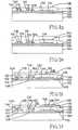
- a processis illustrated for simultaneously producing the following conductive microstructures: a first movable contact 144, a second movable contact 146, a first interconnect 148, a second interconnect 150, an electrode interconnect 152, a third interconnect 154, and an electrical connection 156.
- the dimensions of movable electrode 138are 180 x 350 microns.
- movable electrode 138can be any other suitable dimensions. These dimensions are determined by desired functionality and manufacturability requirements.
- the dimensions of electrode interconnect 152are 180 x 350 microns.
- recesses 158, 160, and 162are etched through structural layer 142.
- a recess 164is etched into structural layer 142.
- Recess 158is patterned and etched through structural layer 142 and into first sacrificial layer 136 for forming first interconnect 148 and first movable contact 144.
- First movable contact 144 and second movable contact 146comprise a conductive material such as copper, gold, aluminum, their alloys or composites, or any other suitable metal known to those of skill in the art.
- Recess 158is etched into first sacrificial layer 136 so that first movable contact 144 extends beyond structural layer 142.
- Recess 160is patterned and etched through structural layer 142 and into first sacrificial layer 136 for forming second interconnect 150 and second movable contact 146.
- Recess 160is etched into first sacrificial layer 136 so that second movable contact 146 extends beyond structural layer 142.
- Recess 162is patterned and etched through structural layer 142 for forming third interconnect 154 to movable electrode 138.
- Recess 164is patterned and etched through structural layer 142 to form a suspended end of the beam and the unconstrained side of the beam.
- Recesses 158, 160, 162, and 164can be etched by a dry or wet etch process or patterned by other suitable methods known to those of skill in the art.
- the simultaneous fabrication of recesses 158, 160, 162, and 164provide simplification of the overall process relative to the number of photolithography steps and mask layers.
- the formation of recesses 160, 162, and 164 through structural layer 142requires a different process than the formation into first sacrificial layer 136.
- recess 164can be formed in another step because it is only required to be formed through structural layer 142 and not first sacrificial layer 136. Additionally, recess 164 can be formed by patterning and etching structural layer 142 at the free end of the beam and along the sides, but not at the portion of structural layer that attaches to substrate 100. The sequence of the alternative steps must be determined by simplicity and compatibility. Alternatively, first movable contact 144 and second movable contact 146 can be formed by another pattern in fourth conductive layer 140. Alternatively, first movable contact 144 and second movable contact 146 can be patterned and formed in first sacrificial layer 136.
- a pattern in fourth conductive layer 140can coincide with the pattern for first movable contact 144 and second movable contact 146 as formed in first sacrificial layer 136.
- First movable contact 144 and second movable contact 146can be patterned and formed by methods known to those with skill in the art.
- Movable contacts 144 and 146are required to establish electrical communication between first stationary contact 130 and second stationary contact 132.
- the electrical communicationis established when first movable contact 144 is in close proximity to first stationary contact 130 and when second movable contact is in close proximity to first stationary contact 130.
- the electrical communicationis completed through a path that includes first stationary contact 130, first movable contact 144, first interconnect 148 (the electrical connection described in further detail below), second interconnect 150 (the electrical connection described in further detail below), and second movable contact 146.
- First movable contact 144 and second movable contact 146are shown in the plane of the cross-section with first movable contact 144 nearest the free end of the beam and second movable contact 146.
- first movable contact 144establishes contact with first stationary contact 130 and then second movable contact 146 establishes contact with second stationary contact 132.
- the primary configurationhas first movable contact 144 and second movable contact 146 located at the same position along the length of the beam. In this configuration, first movable contact 144 and second movable contact 146 are separated relative to each other as shown in FIG. 1U . Movable contacts 144 and 146 establish contact with stationary contacts 130 and 132, respectively.
- the second movable contactfunctions as a static contact at the fixed end of the beam.
- the static contactestablishes electrical connection through a via in structural layer 142 to second movable contact 146 at the fixed end of the beam.
- the electrical connection between second movable contact 146 and the static contactwill transverse the length of the beam from the location of second movable contact 146 at the free end of the beam to the static contact at the fixed end of the beam.
- a fifth conductive layer 166is deposited on first sacrificial layer 136 and structural layer 142.
- Fifth conductive layer 166is patterned by a method as described above.
- Electrode interconnect 152 and electrical connection 156are formed. Electrode interconnect 152 is a structural match to movable electrode 138. In one alternative, the geometry and dimensions of electrode interconnect 152 and movable electrode 138 are matched exactly. The exact matching of these structures provide more robustness to film stress and temperature induced deformation of the beam. In another alternative for achieving similar robustness to film stress and temperature induced beam deformation, electrode interconnect 152 and movable electrode 138 are designed to be structurally similar but geometrically and dimensionally different. The structural response of electrode interconnect 152 is designed to be similar to movable electrode 138 to minimize the effects and variations due to the film stresses and temperature independent of the geometry or dimensions matching.
- electrical connection 164connects first movable contact 144 and second movable contact 146 via first interconnect 148 and second interconnect 150.
- Electrode interconnect 152provides an electrical connection to a voltage source (not shown) via electrical connection 164.
- Movable electrode 138is provided an electrical connection to the voltage source via another electrical connection (not shown).
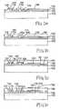
- first sacrificial layer 136is removed to form a trilayered beam, generally designated 168.
- First sacrificial layer 136can be removed by any suitable method known to those of skill in the art.
- the MEMS switchis illustrated in an "open” position wherein a gap exists between first movable contact 144 and first stationary contact 130 and between second movable contact 146 and second stationary contact 132. In the "open" position, no electrical connection is established between first movable contact 144 and first stationary contact 130 and between second movable contact 146 and second stationary contact 132. Movement of the MEMS switch to a "closed” position can be effected by application of a voltage across stationary electrode 134 and electrical connection 156 via a voltage source. Voltage source can be electrically connected to stationary electrode 134 and electrical connection 156 by a suitable method known to those of skill in the art.
- Movable electrode 138is energized by the voltage application due to the electrical connection of movable electrode 138 through electrode interconnect 152, third interconnect 154, and electrical connection 156.
- an equal and opposite chargeis generated on stationary electrode 134 and movable electrode 138.
- the charge distribution on the opposing electrodesproduces an electrostatic force that is balanced by the elastic forces of the now deformed beam.
- the stability pointis defined by the inability of the elastic forces to maintain equilibrium with the electrostatic forces and the beam snaps through to establish contact.
- the voltagecan continue to be increased, thereby increasing the contact force and reducing the contact resistance up to the limit of the isolation limits of the beam.
- the isolation limitsare defined by a dielectric breakdown, a gas discharge or breakdown, or an elastic breakdown where the beam snaps through a second time to short the electrodes. Methods known to those skilled in the art can be applied to maximize this isolation.
- the voltagecan be decreased until the release voltage is reached where the beam snaps away from the substrate to "open" the contacts.
- the release voltageis less, typically, than the pull in voltage that determined closure of the contacts. A monotonic excursion of the voltage-time function is not required to facilitate this operation, such that the switch operates rather instantaneously.
- the electrical connection 156 and stationary electrode 134are designed for structural similarity so that the beam is largely flat in the "open” position. Additionally, this structural similarity enhances the performance over temperature because of the thermomechanical balance across the beam.
- the fabricated MEMS switchis illustrated in a "closed" position wherein first movable contact 144 contacts first stationary contact 130 and second movable contact 146 contacts second stationary contact 132.
- an electrical connectionis established between first movable contact 144 and first stationary contact 130 and between second movable contact 146 and second stationary contact 132.
- electrical connectionis established between first conductive microstructure 106 and second conductive microstructure 116 by the configuration of components 148, 150, and 164.
- the MEMS switchis returned to an "open" position when the voltage applied across movable electrode 138 and stationary electrode 134 is reduced sufficiently such that the reflexive force of structural layer 142 returns beam 168 to a natural position.
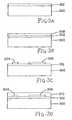
- a substrate 300is provided.
- Substrate 300comprises silicon.
- substrate 300can comprise any other suitable material known to those of skill in the art. If the composition of substrate 300 is chosen to be a conductive or semi-conductive material, a non-conductive, first dielectric layer 302 is deposited on the top surface of substrate 300, or at least a portion of the top surface where electrical contacts or conductive regions are desired.
- FIG. 3B - 3Ca process for producing a stationary contact 304 and a stationary electrode 306 is illustrated.
- a first conductive layer 308is deposited on first dielectric layer 302.
- First conductive layer 308is patterned as described above.
- stationary contact 304 and stationary electrode 306are formed simultaneously.
- stationary contact 304 and stationary electrode 306can be formed in separate processes.
- a sacrificial layer 310is deposited to a uniform thickness such that its top surface is preferably planarized.
- Sacrificial layer 310defines the gap between stationary contact 304 and stationary electrode 306 and a trilayered beam structure, described in detail below.
- Sacrificial layer 310comprises a polymer.
- sacrificial layer 310can be a metal, dielectric or any other suitable material known to those of skill in the art such that the removal chemistry is compatible with the other electrical and structural materials.
- sacrificial layer 310can be patterned and etched such that contact bumps are recessed below structures formed on the underside of the beam structure or to form a larger structure that is recessed.
- recessescan be formed by other suitable means known to those of skill in the art.
- FIGs. 3E - 3Fa process for producing a movable contact 312 and a movable electrode 314 is illustrated.
- grooves 316, 318 and 320are etched in sacrificial layer 310.
- Grooves 316 and 318are etched in sacrificial layer 310 for movable contact 312 and movable electrode 314, respectively.
- Groove 320is formed for forming a structure to attach the beam to substrate 300 and suspend the beam above components 304 and 306.
- a conductive layeris deposited on sacrificial layer 310 until grooves 316 and 318 are filled.
- the conductive layeris patterned as described above to form movable contact 312 and movable electrode 314.
- a structural layer 322is deposited on movable contact 312, movable electrode 314, sacrificial layer 310, and first dielectric layer 302.
- Structural layer 322comprises oxide in this embodiment.
- a process for simultaneously producing the following conductive microstructuresa contact interconnect 324, an electrode interconnect 326, and interconnect vias 328 and 330.
- recesses 332 and 334are etched into structural layer 322 for forming interconnect vias 328 and 330, respectively.
- Recesses 332 and 334are etched through structural layer 322 to movable contact 312 and movable electrode 314.
- a second conductive layer 336is deposited on structural layer 322 and into recesses 332 and 334 as shown for forming an electrical connection from movable contact 312 and movable electrode 314 to the top surface of structural layer 322.
- second conductive layer 336is patterned for forming contact interconnect 324 and electrode interconnect 326 as shown in FIG. 3J .
- Interconnect vias 328 and 330can be formed by another conductive layer that would precede the deposition of second conductive layer 336 described above.
- Stationary contact 304, stationary electrode 306, movable contact 312, movable electrode 314, electrode interconnect 326, contact interconnect 324, and interconnect vias 328 and 330comprise a metal in this embodiment.
- movable electrode 314 and electrode interconnect 326are fabricated of the same material and dimensioned the same in order to perform two functions.
- the mechanical balanceis provided because of the elastic symmetry, because the films are deposited in the same way to produce a symmetric stress field, and because the thermal expansion properties are symmetric.
- the elastic symmetryis preserved by using the same material and by using the same dimensions.
- the symmetric stress fieldis produced by depositing the same materials using the same process and thicknesses.
- the symmetric thermal expansion propertiesminimize any variation in the switch operation with respect to temperature because the same material is on either side of structural layer 322.
- stationary contact 304, stationary electrode 306, movable electrode 314, movable contact 312, electrode interconnect 326, contact interconnect 324, and interconnect vias 328 and 330could be different materials or different alloys of the same materials.
- the material selectionminimizes contact resistance and failures such as stiction.
- sacrificial layer 310is removed to form a trilayered beam, generally designated 338.
- Sacrificial layer 310can be removed by any suitable method known to those of skill in the art.
- the MEMS switchis illustrated in an "open” position. In a “closed” position, beam 338 is deflected towards substrate 300 and movable contact 312 contacts stationary contact 304. As described above, a voltage can be applied across electrode interconnect 326 and stationary electrode 306 for moving the MEMS switch into a "closed” position.
Landscapes
- Engineering & Computer Science (AREA)
- Microelectronics & Electronic Packaging (AREA)
- Computer Hardware Design (AREA)
- Chemical & Material Sciences (AREA)
- Power Engineering (AREA)
- General Physics & Mathematics (AREA)
- Physics & Mathematics (AREA)
- Manufacturing & Machinery (AREA)
- Condensed Matter Physics & Semiconductors (AREA)
- Analytical Chemistry (AREA)
- Ceramic Engineering (AREA)
- Materials Engineering (AREA)
- Micromachines (AREA)
- Gyroscopes (AREA)
- Internal Circuitry In Semiconductor Integrated Circuit Devices (AREA)
- Pressure Sensors (AREA)
- Mechanical Light Control Or Optical Switches (AREA)
- Measurement And Recording Of Electrical Phenomena And Electrical Characteristics Of The Living Body (AREA)
- Multi-Conductor Connections (AREA)
- Buffer Packaging (AREA)
- Wire Bonding (AREA)
- Lead Frames For Integrated Circuits (AREA)
- Coupling Device And Connection With Printed Circuit (AREA)
- Design And Manufacture Of Integrated Circuits (AREA)
- Air Bags (AREA)
- Treatment Of Fiber Materials (AREA)
- Switches Operated By Changes In Physical Conditions (AREA)
- Thermally Actuated Switches (AREA)
- Bending Of Plates, Rods, And Pipes (AREA)
- Apparatuses And Processes For Manufacturing Resistors (AREA)
- Cooling Or The Like Of Semiconductors Or Solid State Devices (AREA)
Abstract
Description
- The present invention relates to a method for fabricating a microscale switch having a trilayered beam.
US 6,057,520 A discloses an arc resistant high voltage micro-machined electrostatic switch. The MEMS device known from this document comprises a micro-electronic substrate, a substrate electrode, first and second contact sets, an insulator, and a moveable composite. The moveable composite overlies the substrate and the substrate electrode. In cross section, the moveable composite comprises an electrode layer and a biasing layer. In length, the moveable composite comprises a fixed portion attached to the underlying substrate, a medial portion, and a distal portion moveable with respect to the substrate electrode. Each contact set has at least one composite contact attached to the moveable composite and preferably at least one substrate contact attached to the substrate.US 5,702,569 A discloses a method for manufacturing a thin film actuated mirror having a stable elastic member. The method includes the steps of: forming a thin film sacrificial layer; depositing an elastic layer on top of the thin film sacrificial layer by using a CVD method; forming an actuating structure on top of the elastic layer, the actuating structure having a first thin film electrode, a thin film electrodisplacive member, a second thin film electrode and an elastic member; and removing the thin film sacrificial layer.- An electrostatic MEMS switch is a switch operated by an electrostatic charge and manufactured using micro-electro-mechanical systems (MEMS) techniques. A MEMS switch can control electrical, mechanical, or optical signal flow. MEMS switches have typical application to telecommunications, such as DSL switch matrices and cell phones, Automated Testing Equipment (ATE), and other systems that require low cost switches or low-cost, high-density arrays.
- As can be appreciated by persons skilled in the art, many types of MEMS switches and related devices can be fabricated by either bulk or surface micromachining techniques or a combination of both types of techniques. Bulk micromachining generally involves sculpting one or more sides of a substrate to form desired three-dimensional structures and devices in the same substrate material. The substrate is composed of a material that is readily available in bulk form, and thus ordinarily is silicon or glass. Wet and/or dry etching techniques are employed in association with etch masks and etch stops to form the microstructures. Etching is typically performed on the backside or frontside of the substrate. The etching technique can generally be either isotropic or anisotropic in nature. Isotropic etching is insensitive to the crystal orientation of the planes of the material being etched (e.g., the etching of silicon using a mixture of hydrofluoric, nitric, and acetic acids (HNA) as the etchant). Anisotropic etchants, such as potassium hydroxide (KOH), tetramethyl ammonium hydroxide (TMAH), and ethylenediamine pyrochatechol (EDP), selectively attack different crystallographic orientations at different rates, and thus can be used to define relatively accurate sidewalls in the etch pits being created. Etch masks and etch stops are used to prevent predetermined regions of the substrate from being etched.
- On the other hand, surface micromachining generally involves forming three-dimensional structures by depositing a number of different thin films on the top of a silicon wafer, but without sculpting the wafer itself. The films usually serve as either structural or sacrificial layers. Structural layers are frequently composed of polysilicon, silicon nitride, silicon dioxide, silicon carbide, or aluminum. Sacrificial layers are frequently composed of polysilicon, photoresist material, polymide, metals, or various kinds of oxides, such as PSG (phosphosilicate glass) and LTO (low-temperature oxide). Successive deposition, etching, and patterning procedures are carried out to arrive at the desired microstructure. In a typical surface micromachining process, a silicon substrate is coated with an isolation layer, and a sacrificial layer is deposited on the coated substrate. Windows are opened in the sacrificial layer, and a structural layer is then deposited and etched. The sacrificial layer is then selectively etched to form a free-standing, movable microstructure such as a beam or a cantilever out of the structural layer. The microstructure is ordinarily anchored to the silicon substrate, and can be designed to be movable in response to an input from an appropriate actuating mechanism.
- Many current MEMS switch designs employ cantilevered beam/plate, or multiply-supported beam/plate geometry for the switching structure. In the case of cantilevered beams/plates, these MEMS switches include a movable, bimaterial beam comprising a structural layer of dielectric material and a layer of metal. Typically, the dielectric material is fixed at one end with respect to the substrate and provides structural support for the beam. The layer of metal is attached on the underside of the dielectric material and forms a movable electrode and a movable contact. The layer can be part of the anchor or attachment to the substrate. The movable beam is actuated in a direction toward the substrate by the application of a voltage difference across the electrode and another electrode attached to the surface of the substrate. The application of the voltage difference to the two electrodes creates an electrostatic field which pulls the beam towards the substrate. The beam and substrate each have a contact which can be separated by an air gap when no voltage is applied, wherein the switch is in the "open" position. When the voltage difference is applied, the beam is pulled to the substrate and the contacts make an electrical connection, wherein the switch is in the "closed" position.
- One of the problems that faces current MEMS switches having a bimaterial beam is curling or other forms of static displacement or deformation of the beam. The static deformation can be caused by a stress mismatch or a stress gradient within the films. At some equilibrium temperature, the mismatch effects can be balanced to achieve a flat bimaterial structure, but this does not correct the temperature effects. The mismatch can be balanced through specific processes (i.e., deposition rates, pressures, methods, etc.), material selection, and geometrical parameters such as thickness. This bimaterial structure of metal and dielectric introduces a large variation in function over temperature, because the metal will typically have a higher thermal expansion rate than the dielectric. Because of the different states of static stress in the two materials, the switch can be deformed with a high degree of variability. Switch failure can result from deformation of the beam. Switch failure can occur when (1) electrical contact cannot be established between the movable and stationary contacts, (2) electrical contact is established without any actuation, or (3) the operational parameters are driven out of the acceptable specification range due to static deformation or because of the deformation introduced as a function of temperature. A second mode of failure is observed when the movable contact and the stationary contact are prematurely closed, resulting in a "short". Because of the deformation of the beam, the actuation voltage is increased or decreased depending on whether it is curved away from the substrate or towards the substrate, respectively. Because of this variability, the available voltage may not be adequate to achieve the desired contact force and thus contact resistance.
- Some current MEMS switch designs having the bimaterial beam attach the metal layer for the movable electrode to the topside of the dielectric material. The metal layer for the moving contact must still be on the underside of the dielectric material. This design can in some instances serve to provide isolation between the movable electrode and the stationary electrode on the substrate; however, this design requires a higher voltage for actuation because the gap distance between the metal layer and the electrode attached to the surface of the substrate is greater. The effective gap is the sum of the gap between the stationary electrode and the dielectric, and the dielectric thickness. Thus, such a design requires greater power consumption and creates problems with regard to dielectric charging.
- A common approach to develop a cross-bar switch array is by a process of forming the cross-bar interconnect structure on a printed wire board (PWB), printed circuit board (PCB), low temperature ceramic composite (LTCC) substrate, or polymer composite substrate and subsequently attaching a switch to the board or substrate. The switch can be attached by a combination of methods such as soldering, wire bonding, bump bonding, flip chip, and other attachment and electric interconnection methods. In this process, the fabrication of the cross-bar interconnect structure is integrated with the MEMS switch process so that they are fabricated on the same substrate with the same process. The advantage of the cross-bar interconnect structure is that an array of input signals can be electrically communicated to a single (or multiple) output of an array of outputs. The array dimensions can be square or rectangular, wherein a square array is an NXN array of N inputs and N outputs and a rectangular array is an NXM array of N inputs and M outputs. The input and output lines of a cross-bar interconnect are electrically connected by the MEMS switch when it is activated in a "closed" position. At each switching node in the cross-bar array, the input/output lines have stationary contact terminals. The integrated MEMS switch functions to establish mechanical and electrical connection between the moving contact and stationary contacts of the input and output lines. The input and output lines communicate through the contact established by the MEMS switch. Alternatively, MEMS switches can be used in a cross-bar array in the usual fashion, if it is attached to the switching nodes of the cross-bar array. This configuration is undesirable because a highly capable fabrication process must be replaced by a less capable assembly process. This will increase the total cost, decrease the quality, complicate the process, and increase the size.
- Therefore, it is desirable to provide a fabrication process for producing a structural element (e.g., a beam, plate, and membrane) to improve yield, performance over temperature, actuation, and quality of MEMS switches. It is also desirable to provide a fabrication process for producing a structural element resistant to deformation caused by parasitic or "self" actuation. It is also desirable to provide a fabrication process for producing a structural element that is robust to process variations, film stresses, and their gradients. Furthermore, it is desirable to provide a method for forming a cross-bar interconnect and MEMS switch in the same fabrication process. It is desirable to provide a method that is flexible so that the MEMS switch can be formed and integrated with cross-bar interconnects that are fabricated in another fashion.
- The invention provides a method for fabricating a microscale switch having a trilayered beam as defined in independent claim 1.
- Preferred embodiments are listed in the dependent claims.
- Exemplary embodiments of the invention will now be explained with reference to the accompanying drawings, of which:
Figures 1A -1V illustrate fabrication steps of a method for fabricating a MEMS switch having a trilayered beam;Figure 2 illustrates a cross-sectional side view of a MEMS switch having a trilayered beam in a "closed" position; andFigures 3A - 3K illustrate fabrication steps of another embodiment of a method for fabricating a MEMS switch having a trilayered beam.- For purposes of the description herein, it is understood that when a component such as a layer or substrate is referred to as being deposited or formed "on" another component, that component can be directly on the other component or, alternatively, intervening components (for example, one or more buffer or transition layers, interlayers, electrodes or contacts) can also be present. Furthermore, it is understood that the terms "disposed on" and "formed on" are used interchangeably to describe how a given component can be positioned or situated in relation to another component. Therefore, it will be understood that the terms "disposed on" and "formed on" do not introduce any limitations relating to particular methods of material transport, deposition, or fabrication.
- Contacts, interconnects, conductive vias, and electrodes of various metals can be formed by sputtering, CVD, or evaporation. If gold, nickel, copper, or PERMALLOY™ (NixFey) is employed as the metal element, an electroplating process can be carried out to transport the material to a desired surface. The chemical solutions used in the electroplating of various metals are generally known. Some metals, such as gold, might require an appropriate intermediate adhesion layer to prevent peeling. Examples of adhesion material often used include chromium, titanium, or an alloy such as titanium tungsten (TiW). To prevent interstitial or intergranular diffusion, diffusion barriers can be required between different layers. Suitable diffusion barriers include titanium nitride (TiN), molybdenum (Mo), nickel (Ni), tantalum nitride (TaN) or any combination thereof. Alternatively, any other suitable diffusion barrier known to those of skill in the art can be used. For example, nickel can be used as a diffusion barrier to the chromium adhesion layer diffusing along the grain boundaries of a gold metalization.
- Conventional lithographic techniques can be employed in accordance with fabrication, such as micromachining, of the invention described herein. Accordingly, basic lithographic process steps such as photoresist application, optical exposure, and the use of developers are not described in detail herein.
- Similarly, generally known etching processes can be suitably employed to selectively remove material or regions of material. An imaged photoresist layer is ordinarily used as a masking template. A pattern can be etched directly into the bulk of a substrate, or into a thin film or layer that is then used as a mask for subsequent etching steps.
- The type of etching process employed in a particular fabrication step (e.g., wet, dry, isotropic, anisotropic, anisotropic-orientation dependent), the etch rate, and the type of etchant used will depend on the composition of material to be removed, the composition of any masking or etch-stop layer to be used, and the profile of the etched region to be formed. As examples, poly-etch (HF:HNO3:CH3COOH) can generally be used for isotropic wet etching. Hydroxides of alkali metals (e.g., KOH), simple ammonium hydroxide (NH4OH), quaternary (tetramethyl) ammonium hydroxide ((CH3)4NOH, also known commercially as TMAH), and ethylenediamine mixed with pyrochatechol in water (EDP) can be used for anisotropic wet etching to fabricate V-shaped or tapered grooves, trenches or cavities. Silicon nitride can typically be used as the masking material against etching by KOH, and thus can used in conjunction with the selective etching of silicon. Silicon dioxide is slowly etched by KOH, and thus can be used as a masking layer if the etch time is short. While KOH will etch undoped silicon, heavily doped (p++) silicon can be used as an etch-stop against KOH as well as the other alkaline etchants and EDP. Silicon oxide and silicon nitride can be used as masks against TMAH and EDP. The preferred metal used to form contacts and interconnects in accordance with the invention is gold and its alloys, which are resistant to EDP. The adhesion layer applied in connection with forming a gold component (e.g., chromium) is also resistant to EDP.
- Commonly known wet etchants can be used to etch materials such as copper, gold, silicon dioxide, and secondary materials such as the adhesion and barrier materials. For example, gold can be etched with an aqueous solution of Kl3 in a temperature range of 20 to 50°C. As another example, chromium (a common adhesive layer) can be wet etched at 25°C is a solution of ceric ammonium nitrate, nitric acid, and H2O. Furthermore, for example, copper can be etched 25°C in a dilute solution of nitric acid. A common method of etching silicon dioxide is with various aqueous solutions of HF or solutions of HF that are buffered with ammonium fluoride.
- It will be appreciated that electrochemical etching in hydroxide solution can be performed instead of timed wet etching. For example, if a p-type silicon wafer is used as a substrate, an etch-stop can be created by epitaxially growing an n-type silicon end layer to form a p-n junction diode. A voltage can be applied between the n-type layer and an electrode disposed in the solution to reverse-bias the p-n junction. As a result, the bulk p-type silicon is etched through a mask down to the p-n junction, stopping at the n-type layer. Furthermore, photovoltaic and galvanic etch-stop techniques are also suitable.
- Dry etching techniques such as plasma-phase etching and reactive ion etching (RIE) can also be used to remove silicon and its oxides and nitrides, as well as various metals. Deep reactive ion etching (DRIE) can be used to anisotropically etch deep, vertical trenches in bulk layers. Silicon dioxide is typically used as an etch-stop against DRIE, and thus structures containing a buried silicon dioxide layer, such as silicon-on-insulator (SOI) wafers, can be used according to the methods of the invention as starting substrates for the fabrication of microstructures. For example of a dry etching process, silicon dioxide can be etched in chemistries involving CF4 + O2, CHF3, C2F6, or C3F8. As another example, gold can be dry etched with C2Cl2F4 or C4 Cl2 F4+O2.
- An alternate patterning process to etching is lift-off. In the lift-off process, the conventional photolithography techniques are used for creating the negative image of the desired pattern. The lift-off process is typically used to pattern metals which are deposited as a continuous film or films when adhesion layers and diffusion barriers are needed. Additionally, it can be used to pattern other materials. The metal is deposited on the regions for patterning and on top of the photoresist mask (negative image). The photoresist and metal on top are removed to leave behind the desired pattern of metal.
- As used herein, the term "conductive" is generally taken to encompass both conducting and semi-conducting materials.
- Examples will now be described with reference to the accompanying drawings.
- Referring to
FIG. 1A - 1V a method for fabricating a MEMS switch having a trilayered beam according to a surface micromachining process of the present invention will now be described. The method of fabrication described herein can be used to fabricate other MEMS devices, such as accelerometers, pressure sensors, optical switches, varactors (variable capacitors), variable inductors, and phase shifters. The method of fabrication can be applied to MEMS switches having a trilayered structure, where the trilayered structure can be a doubly-supported beam (attached to the substrate at two ends), a plate/membrane (with edges constrained in different ways, e.g., with four edges constrained), a rigid plate suspended by a multitude of compliant supports such as torsion beams, folded or unfolded beams, and other suspension systems known to those of skill in the art. Referring specifically toFIG. 1A , a starting wafer orsubstrate 100 is provided, which preferably comprises silicon. Non-limiting examples of materials for use as startingsubstrate 100 include silicon (in single-crystal, polycrystalline, or amorphous forms), silicon oxinitride, glass, quartz, sapphire, zinc oxide, alumina, silica, or one of the various Group III - V compounds in either binary, ternary or quaternary forms (e.g., GaAs, InP, GaN, AlN, AlGaN, InGaAs, and so on). The conductivity of a silicon layer can be modulated by performing known methods of impurity doping. The various forms of silicon oxides (e.g., SiO2, other silicon oxides, and silicate glass) can be used as structural, insulating, or etch-stop layers. As known in the art, these oxides can be preferentially etched in hydrofluoric acid (HF) to form desired profiles. Various methods for adding oxide material to a substrate are known in the art. For example, silicon dioxide can be thermally grown by oxidizing silicon at high temperatures, in either a dry or wet oxidation process. Oxides and glasses, including phosphosilicate glass (PSG), borosilicate glass (BSG), borophoshosilicate glass (BPSG, also termed low-temperature oxide or LTO), as well as silicon-based thin films, can be deposited by chemical vapor deposition (CVD) including atmospheric pressure CVD (APCVD), low-pressure CVD (LPCVD) and low-temperature plasma-enhanced CVD (PECVD), as well as by physical vapor deposition (PVD) such as sputtering, or in some cases by a spin-on process similar to that used to deposit polymers and photoresists. Both stoichiometric and non-stoichiometric silicon nitride can be used as an insulating film, or as a masking layer in conjunction with an alkaline etch solution, and is ordinarily deposited by a suitable CVD method. If the composition of startingsubstrate 100 is chosen to be a conductive or semi-conductive material, a non-conductive, firstdielectric layer 102 is deposited on the top surface ofsubstrate 100, or at least on portions of the top surface where electrical contacts or conductive regions are desired. Next, a first photolithography mask layer orsacrificial layer 104 is deposited to a uniform thickness for planarizing the top surface ofsacrificial layer 104. - Referring to
FIGs. 1B-1C , the process for producing a firstconductive microstructure 106 via a lift-off patterning process is illustrated. In this embodiment, firstconductive microstructure 106 is a cross-bar interconnect suitable for communication with another electrical device. Theconductive microstructure 106 extends into the page to a depth greater than the cross-sectional width. Alternatively, firstconductive microstructure 106 can extend into the page a distance equal to or less than its cross-sectional width. In another alternative, firstconductive microstructure 106 can represent a ground plate that will extend in all directions to completely underlay the MEMS microstructure. Alternatively, firstconductive microstructure 106 can be the fixed plate of a stationary or variable capacitor a part of a planar coil (circular or rectangular) that singularly defines an inductive coil or that is part of a 3-dimensional coil when it is electrically connected to other layers. In yet another embodiment, firstconductive microstructure 106 can be any other suitable conductive microstructure for conducting electricity known to those of skill in the art. - Referring specifically to
FIG. 1B ,first photolithography mask 104 is patterned as shown. A firstconductive layer 108 is deposited on firstsacrificial layer 104 and the exposed portion of firstdielectric layer 102. Firstconductive layer 108 comprises gold or any suitable conductive material known to those skilled in the art. Non-limiting examples of depositing firstconductive layer 108 include sputtering, evaporation, electroplating, and any other suitable method known to those skilled in the art. Firstconductive layer 108 comprises any suitable adhesion material and diffusion barrier material known to those of skill in the art. The adhesion material promotes adhesion of firstconductive layer 108 to firstdielectric layer 102 and adhesion of any subsequent dielectric layers. The diffusion barrier inhibits the diffusion of firstconductive layer 108 into firstdielectric layer 102 and into subsequent conductor or dielectric layers. - Next, a lift-off technique is used for removing the remaining first
photolithography mask layer 104 and firstconductive layer 108 except for the portion forming firstconductive microstructure 106. The lift-off technique comprises immersion in a solvent bath to remove firstphotolithography mask layer 104 and the unwanted portions of firstconductive layer 106. Thus, referring toFIG. 1C , firstconductive microstructure 106 remains formed onsubstrate 100 to perform the function of electrical interconnection, ground/shielding planes, or heat dissipation. Other non-limiting examples of patterning firstconductive microstructure 106 includes etching, milling, electroplating, electroless plating, and any other suitable method known to those skilled in the art. - Referring to
FIG. 1D , asecond dielectric layer 110 is deposited on firstdielectric layer 102 and firstconductive microstructure 106.Second dielectric layer 110 is conformal to firstdielectric layer 102 and firstconductive microstructure 106. Alternatively, firstdielectric layer 102 can be overdeposited and planarized by any suitable method known to those skilled in the art. A planarization technique such as chemical mechanical planarization (CMP) can be implemented after deposition of seconddielectric layer 110 to provide a planar surface for subsequent layers. An alternative planarization method is the utilization of a spin-on dielectric that is self-planarizing. As shown inFIG. 1D ,second dielectric layer 110 is not planarized. If the surface is not planarized, the deposited thickness of seconddielectric layer 110 will define the thickness of the interlayer dielectric. If the surface is planarized, the dielectric will be deposited to a thickness greater than the thickness of firstconductive layer 108 and seconddielectric layer 110. The CMP process can remove excess material until the surface is planar and the desired interlayer dielectric thickness is achieved. - Referring to
FIGs. 1E ― 1G, a process for forming arecess 112 to place a first conductive via114 and a secondconductive microstructure 116 is illustrated. In this embodiment, secondconductive microstructure 116 is a cross-bar interconnect for providing an electrical connection to another electrical device. Alternatively, secondconductive microstructure 116 can be any other suitable conductive microstructure known to those of skill in the art. Referring specifically toFIG. 1E , an etching and patterning process is performed to formrecess 112 through seconddielectric layer 110 to firstconductive microstructure 106. Referring now toFIG. 1F , a secondconductive layer 118 is deposited on firstconductive microstructure 106 and inrecess 112 to seconddielectric layer 110. Thus,recess 112 is filled with a conductive material to form first conductive via114. First conductive via114 performs the function of electrical interconnection to firstconductive microstructure 106, as described in further detail below. In an alternative embodiment, an electrical interconnection can be made to firstconductive microstructure 106 by depositing a plug metal inrecess 112. The plug material can be a material different from that of firstconductive microstructure 106 or secondconductive layer 118. Secondconductive layer 118 comprises any suitable adhesion material and diffusion barrier material. The adhesion material promotes adhesion of secondconductive layer 108 to seconddielectric layer 110 and adhesion of any subsequent dielectric layers. The diffusion barrier inhibits the diffusion ofsecond conductor layer 118 intofirst conductor layer 108,second dielectric layer 110, and into subsequent conductor or dielectric layers. - Referring now to
FIG. 1G , secondconductive microstructure 116 is shown formed from the patterning and etching of secondconductive layer 118. Secondconductive microstructure 116 performs electrical interconnection as described in further detail below. Secondconductive microstructure 116 can extend into the page to a depth greater than the cross-sectional width of secondconductive microstructure 116. In this embodiment of the cross-bar interconnect, secondconductive microstructure 116 will extend perpendicular (to the left and right) to firstconductive microstructure 106. Alternatively, secondconductive microstructure 116 can extend into the depth of the page by a distance on the order of the cross-sectional width. In this embodiment, the purpose of secondconductive microstructure 116 is only for electrical connection between firstconductive layer 108 and secondconductive layer 118. In another application, secondconductive microstructure 116 can represent a ground plate that will extend in all directions to completely underlay the MEMS switch. Alternatively, secondconductive microstructure 116 can be the fixed plate of a stationary or variable capacitor or part of a planar coil that singularly defines an inductive coil or that is part of a 3-dimensional coil when it is electrically connected to other layers. Furthermore, secondconductive microstructure 116 can be any suitable conductive microstructure known to those of skill in the art. The portion of first conductive via114 extending beyond the surface of seconddielectric layer 110 is etched away. - In the process for forming first conductive via114 and second
conductive microstructure 116 described above, secondconductive microstructure 116 and first conductive via114 are formed simultaneously. Alternatively, the material for first conductive via114 can be deposited independently of secondconductive microstructure 116. The purpose of depositing and patterning first conductive via114 is to fill first conductive via114 to the surface of seconddielectric layer 110. Next, secondconductive microstructure 116 is deposited and patterned as described above. An alternative process for depositing and patterning first conductive via114 is by a Damascene process. In a Damascene process,second dielectric layer 110 is planarized as described above. An etching and patterning process is performed to form arecess 112 through seconddielectric layer 110 to firstconductive microstructure 106 or other patterned microstructure in firstconductive layer 108. The surface of seconddielectric layer 110 is planar except forrecess 112. Secondconductive layer 118 is deposited on seconddielectric layer 110. Secondconductive layer 118 is deposited on firstconductive microstructure 106 and inrecess 112 to seconddielectric layer 110.Recess 112 is filled with a conductive material to form first conductive via114. Secondconductive layer 118 can be planarized by any suitable method known to those of skill in the art. A planarization technique such as chemical mechanical planarization (CMP) can be implemented after deposition of secondconductive layer 118 to remove all conductive material of secondconductive layer 118 except the conductive material that remains to form first conductive via114. Secondconductive microstructure 116 is patterned and formed as described above. - Referring to
FIG. 1H , a thirddielectric layer 120 is deposited on seconddielectric layer 110, secondconductive microstructure 116, and first conductive via114 to produce a conformal surface. Alternatively, the surface of thirddielectric layer 120 can be planarized as described above. - Referring to
FIGs. 1I ― 1K , a process for extending first conductive via114 and forming a second conductive via122 is illustrated. Referring specifically toFIG. 1I , an etching and patterning process is performed to formrecesses Recess 124 extends from the top surface of thirddielectric layer 120 to secondconductive microstructure 116.Recess 126 extends from the top surface of thirddielectric layer 120 to first conductive via114. Referring toFIG. 1J , a thirdconductive layer 128 is deposited on secondconductive microstructure 116, first conductive via114, and thirddielectric layer 120. Thirdconductive layer 128 fillsrecesses FIG. 1K , third conductive layer128 (shown inFIG. 1J ) is patterned and etched to form the extension to first conductive via114 and second conductive via122 by the methods described above. Second conductive via122 performs the function of electrical interconnection to secondconductive microstructure 116. Alternatively, second conductive via122 and the connection to first conductive via114 can be formed by the Damascene technique described above or by other suitable methods known to those of skill in the art. - Referring to
FIGs. 1L ― 1M , a process for producing a firststationary contact 130, a secondstationary contact 132, and astationary electrode 134 is illustrated. Referring toFIG. 1L , a conductive layer is deposited on first conductive via114, second conductive via122, and thirddielectric layer 120. The conductive layer is patterned as described above. Referring toFIG. 1M , firststationary contact 130, secondstationary contact 132, andstationary electrode 134 are formed simultaneously. Alternatively, firststationary contact 130 and secondstationary contact 132 can be formed preceding or following the formation ofstationary electrode 134. This sequence of formation will allow firststationary contact 130 and secondstationary contact 132 to be formed from different conductive materials, patterned by different patterning methods, or deposited by different deposition methods thanstationary electrode 134. For example, firststationary contact 130 can be formed by evaporation deposition and etching. Alternatively, a via plug, a stud, a post, electrical interconnection, transmission lines, waveguides, stationary actuation electrodes, stationary contact electrodes, electrode interconnects, or any other suitable structure known to those of skill in the art can be formed. Firststationary contact 130, a secondstationary contact 132, and astationary electrode 134 are formed simultaneously in this process. Alternatively,components - First
stationary contact 130, secondstationary contact 132, andstationary electrode 134 comprise a conductive material such as gold or another suitable metal known to those of skill in the art. Alternatively, firststationary contact 130, secondstationary contact 132, andstationary electrode 134 can comprise a semiconductor such as polysilicon, a conductive polymer, or any other suitable conductive material known to those of skill in the art. If firststationary contact 130 and secondstationary contact 132 are made of a different material thanstationary electrode 134,stationary electrode 134 are preferably made of a much lower conductivity. Firststationary contact 130 and secondstationary contact 132 should be of very high conductivity material such as copper, aluminum, gold, or their alloys or composites. - Referring to
FIG. 1N , a firstsacrificial layer 136 is deposited to a uniform thickness such that its top surface is preferably planarized. Firstsacrificial layer 136 defines the gap betweencomponents sacrificial layer 136 comprises a polymer. Alternatively, firstsacrificial layer 136 can be a metal, semiconductor, dielectric or any other suitable material known to those of skill in the art such that the removal chemistry is compatible with the other electrical and structural materials. Primarily, firstsacrificial layer 136 defines the gap between components onsubstrate 100 and the trilayered beam structure. Alternatively, a conductive material can form electrical interconnects, transmission lines, waveguides, stationary capacitor plates, or stationary inductor elements. Alternatively, a dielectric or polymer sacrificial layer can be used to define an interlayer dielectric to increase capacity between stationary capacitor plates, to increase isolation between stationary electrodes, as a mechanical support or spring element for the trilayered beam structure. In these embodiments, firstsacrificial layer 136 is preferably protected by layers of the trilayered beam structure during the release etch described in more detail below. - Referring to
FIGs. 1O - 1P , a process for producing amovable electrode 138 is illustrated. Referring toFIG. 1O , a fourthconductive layer 140 is deposited on firstsacrificial layer 136. Fourthconductive layer 140 is patterned as described above. Referring toFIG. 1P ,movable electrode 138 is formed.Movable electrode 138 comprises a conductive material such as gold or any other suitable metal. Alternatively,movable electrode 138 can comprise a semiconductor such as polysilicon, a conductive polymer, or any other suitable conductive material known to those skilled in the art. Alternatively, fourthconductive layer 140 can be patterned to form a movable contact electrode, a movable contact bar, a movable plate of a variable capacitor, a movable inductor of a variable inductor, a section of an air bridge transmission line/waveguide, electrical interconnects, electrode interconnect layers, a structural element of the trilayered beam structure, and as part of the attachment between the structural layer described below, andsubstrate 100. - Referring to
FIGs. 1Q - 1R , a process for producing astructural layer 142 for providing structure for the beam and attaching the beam tosubstrate 100 is illustrated. Referring specifically toFIG. 1Q , firstsacrificial layer 136 is patterned and etched (dry or wet) through to thirddielectric layer 120 as shown for forming a structure to attach the beam tosubstrate 100 and suspend the beam abovecomponents sacrificial layer 136 can be patterned by other suitable methods known to those of skill in the art such as lift-off, electroplating, electroless plating, or photoexposure and ashing. Primarily, the patterning of firstsacrificial layer 136 defines the location of the attachment portion of the trilayered beam structure tosubstrate 100. Alternatively, firststructural layer 142 is patterned to form insulating interfaces for electrical interconnects, transmission lines, waveguides, stationary capacitor plates, stationary inductor elements, or interlayer dielectrics. Referring toFIG. 1R ,structural layer 142 is deposited on thirddielectric layer 120, firstsacrificial layer 136, andmovable electrode 138.Structural layer 142 preferably comprises silicon dioxide which can be deposited by sputtering, evaporation, spin-on, oxidations, or other suitable methods known to those of skill in the art. Alternatively,structural layer 142 can comprise silicon nitride, silicon oxynitride, aluminum oxide, polymers, or any other suitable non-conductive, resilient material known to those of skill in the art.Structural layer 142 is resilient and provides desired isolation betweenstationary contacts structural layer 142 provides isolation betweenstationary electrode 134 and the movable electrodes on the beam as described below. - Referring to
FIGs. 1S - 1U , a process is illustrated for simultaneously producing the following conductive microstructures: a firstmovable contact 144, a secondmovable contact 146, afirst interconnect 148, asecond interconnect 150, anelectrode interconnect 152, athird interconnect 154, and anelectrical connection 156. Preferably, the dimensions ofmovable electrode 138 are 180 x 350 microns. Alternatively,movable electrode 138 can be any other suitable dimensions. These dimensions are determined by desired functionality and manufacturability requirements. Preferably, the dimensions ofelectrode interconnect 152 are 180 x 350 microns. Referring specifically toFIG. 1S , recesses158, 160, and162 are etched throughstructural layer 142. Additionally, arecess 164 is etched intostructural layer 142.Recess 158 is patterned and etched throughstructural layer 142 and into firstsacrificial layer 136 for formingfirst interconnect 148 and firstmovable contact 144. Firstmovable contact 144 and secondmovable contact 146 comprise a conductive material such as copper, gold, aluminum, their alloys or composites, or any other suitable metal known to those of skill in the art. Recess 158 is etched into firstsacrificial layer 136 so that firstmovable contact 144 extends beyondstructural layer 142. Recess160 is patterned and etched throughstructural layer 142 and into firstsacrificial layer 136 for formingsecond interconnect 150 and secondmovable contact 146. Recess160 is etched into firstsacrificial layer 136 so that secondmovable contact 146 extends beyondstructural layer 142.Recess 162 is patterned and etched throughstructural layer 142 for formingthird interconnect 154 tomovable electrode 138.Recess 164 is patterned and etched throughstructural layer 142 to form a suspended end of the beam and the unconstrained side of the beam.Recesses recesses recesses structural layer 142 and into firstsacrificial layer 136 to formfirst interconnect 148 and firstmovable contact 144. The formation ofrecesses structural layer 142 requires a different process than the formation into firstsacrificial layer 136. Additionally,recess 164 can be formed in another step because it is only required to be formed throughstructural layer 142 and not firstsacrificial layer 136. Additionally,recess 164 can be formed by patterning and etchingstructural layer 142 at the free end of the beam and along the sides, but not at the portion of structural layer that attaches tosubstrate 100. The sequence of the alternative steps must be determined by simplicity and compatibility. Alternatively, firstmovable contact 144 and secondmovable contact 146 can be formed by another pattern in fourthconductive layer 140. Alternatively, firstmovable contact 144 and secondmovable contact 146 can be patterned and formed in firstsacrificial layer 136. Additionally, a pattern in fourthconductive layer 140 can coincide with the pattern for firstmovable contact 144 and secondmovable contact 146 as formed in firstsacrificial layer 136. Firstmovable contact 144 and secondmovable contact 146 can be patterned and formed by methods known to those with skill in the art.Movable contacts stationary contact 130 and secondstationary contact 132. The electrical communication is established when firstmovable contact 144 is in close proximity to firststationary contact 130 and when second movable contact is in close proximity to firststationary contact 130. The electrical communication is completed through a path that includes firststationary contact 130, firstmovable contact 144, first interconnect148 (the electrical connection described in further detail below), second interconnect 150 (the electrical connection described in further detail below), and secondmovable contact 146. Firstmovable contact 144 and secondmovable contact 146 are shown in the plane of the cross-section with firstmovable contact 144 nearest the free end of the beam and secondmovable contact 146. In this embodiment, firstmovable contact 144 establishes contact with firststationary contact 130 and then secondmovable contact 146 establishes contact with secondstationary contact 132. Alternatively, the primary configuration has firstmovable contact 144 and secondmovable contact 146 located at the same position along the length of the beam. In this configuration, firstmovable contact 144 and secondmovable contact 146 are separated relative to each other as shown inFIG. 1U .Movable contacts stationary contacts - In another embodiment, there is a single movable contact and stationary contact. In this embodiment, the second movable contact functions as a static contact at the fixed end of the beam. The static contact establishes electrical connection through a via in
structural layer 142 to secondmovable contact 146 at the fixed end of the beam. In this embodiment, the electrical connection between secondmovable contact 146 and the static contact will transverse the length of the beam from the location of secondmovable contact 146 at the free end of the beam to the static contact at the fixed end of the beam. - Referring to
FIG. 1T , a fifthconductive layer 166 is deposited on firstsacrificial layer 136 andstructural layer 142. Fifthconductive layer 166 is patterned by a method as described above. - Referring to
FIG. 1U ,electrode interconnect 152 andelectrical connection 156 are formed.Electrode interconnect 152 is a structural match tomovable electrode 138. In one alternative, the geometry and dimensions ofelectrode interconnect 152 andmovable electrode 138 are matched exactly. The exact matching of these structures provide more robustness to film stress and temperature induced deformation of the beam. In another alternative for achieving similar robustness to film stress and temperature induced beam deformation,electrode interconnect 152 andmovable electrode 138 are designed to be structurally similar but geometrically and dimensionally different. The structural response ofelectrode interconnect 152 is designed to be similar tomovable electrode 138 to minimize the effects and variations due to the film stresses and temperature independent of the geometry or dimensions matching. As shown,electrical connection 164 connects firstmovable contact 144 and secondmovable contact 146 viafirst interconnect 148 andsecond interconnect 150.Electrode interconnect 152 provides an electrical connection to a voltage source (not shown) viaelectrical connection 164.Movable electrode 138 is provided an electrical connection to the voltage source via another electrical connection (not shown). - Referring to
FIG. 1V , the final step in fabricating the MEMS switch is illustrated. In this step, firstsacrificial layer 136 is removed to form a trilayered beam, generally designated168. Firstsacrificial layer 136 can be removed by any suitable method known to those of skill in the art. - The MEMS switch is illustrated in an "open" position wherein a gap exists between first
movable contact 144 and firststationary contact 130 and between secondmovable contact 146 and secondstationary contact 132. In the "open" position, no electrical connection is established between firstmovable contact 144 and firststationary contact 130 and between secondmovable contact 146 and secondstationary contact 132. Movement of the MEMS switch to a "closed" position can be effected by application of a voltage acrossstationary electrode 134 andelectrical connection 156 via a voltage source. Voltage source can be electrically connected tostationary electrode 134 andelectrical connection 156 by a suitable method known to those of skill in the art.Movable electrode 138 is energized by the voltage application due to the electrical connection ofmovable electrode 138 throughelectrode interconnect 152,third interconnect 154, andelectrical connection 156. When the voltage is applied, an equal and opposite charge is generated onstationary electrode 134 andmovable electrode 138. The charge distribution on the opposing electrodes produces an electrostatic force that is balanced by the elastic forces of the now deformed beam. As the voltage is increased, the charge increases in a non-uniform and non-linear fashion across the surface of the beam until an instability point is reached. The stability point is defined by the inability of the elastic forces to maintain equilibrium with the electrostatic forces and the beam snaps through to establish contact. At this point, the voltage can continue to be increased, thereby increasing the contact force and reducing the contact resistance up to the limit of the isolation limits of the beam. The isolation limits are defined by a dielectric breakdown, a gas discharge or breakdown, or an elastic breakdown where the beam snaps through a second time to short the electrodes. Methods known to those skilled in the art can be applied to maximize this isolation. Alternatively, the voltage can be decreased until the release voltage is reached where the beam snaps away from the substrate to "open" the contacts. The release voltage is less, typically, than the pull in voltage that determined closure of the contacts. A monotonic excursion of the voltage-time function is not required to facilitate this operation, such that the switch operates rather instantaneously. Theelectrical connection 156 andstationary electrode 134 are designed for structural similarity so that the beam is largely flat in the "open" position. Additionally, this structural similarity enhances the performance over temperature because of the thermomechanical balance across the beam. - Referring to
FIG. 2 , the fabricated MEMS switch is illustrated in a "closed" position wherein firstmovable contact 144 contacts firststationary contact 130 and secondmovable contact 146 contacts secondstationary contact 132. Thus, in the "closed" position, an electrical connection is established between firstmovable contact 144 and firststationary contact 130 and between secondmovable contact 146 and secondstationary contact 132. Additionally, electrical connection is established between firstconductive microstructure 106 and secondconductive microstructure 116 by the configuration ofcomponents movable electrode 138 andstationary electrode 134 is reduced sufficiently such that the reflexive force ofstructural layer 142 returnsbeam 168 to a natural position. - Referring to
FIGs. 3A - 3K , another embodiment of a method for fabricating a MEMS switch having a trilayered beam according to a surface micromachining process of the present invention will now be described. Referring specifically toFIG. 3A , asubstrate 300 is provided.Substrate 300 comprises silicon. Alternatively,substrate 300 can comprise any other suitable material known to those of skill in the art. If the composition ofsubstrate 300 is chosen to be a conductive or semi-conductive material, a non-conductive, firstdielectric layer 302 is deposited on the top surface ofsubstrate 300, or at least a portion of the top surface where electrical contacts or conductive regions are desired. - Referring to
FIG. 3B - 3C , a process for producing astationary contact 304 and astationary electrode 306 is illustrated. Referring toFIG. 3B , a firstconductive layer 308 is deposited on firstdielectric layer 302. Firstconductive layer 308 is patterned as described above. Referring toFIG. 3C ,stationary contact 304 andstationary electrode 306 are formed simultaneously. Alternatively,stationary contact 304 andstationary electrode 306 can be formed in separate processes. - Referring to
FIG. 3D , asacrificial layer 310 is deposited to a uniform thickness such that its top surface is preferably planarized.Sacrificial layer 310 defines the gap betweenstationary contact 304 andstationary electrode 306 and a trilayered beam structure, described in detail below.Sacrificial layer 310 comprises a polymer. Alternatively,sacrificial layer 310 can be a metal, dielectric or any other suitable material known to those of skill in the art such that the removal chemistry is compatible with the other electrical and structural materials. - Alternatively,
sacrificial layer 310 can be patterned and etched such that contact bumps are recessed below structures formed on the underside of the beam structure or to form a larger structure that is recessed. Alternatively, recesses can be formed by other suitable means known to those of skill in the art. - Referring to
FIGs. 3E - 3F , a process for producing amovable contact 312 and amovable electrode 314 is illustrated. Referring toFIG. 3E ,grooves sacrificial layer 310.Grooves sacrificial layer 310 formovable contact 312 andmovable electrode 314, respectively.Groove 320 is formed for forming a structure to attach the beam tosubstrate 300 and suspend the beam abovecomponents FIG. 3F , a conductive layer is deposited onsacrificial layer 310 untilgrooves movable contact 312 andmovable electrode 314. - Referring to
FIG. 3G , astructural layer 322 is deposited onmovable contact 312,movable electrode 314,sacrificial layer 310, and firstdielectric layer 302.Structural layer 322 comprises oxide in this embodiment. - Referring to
FIG. 3H - 3J , a process for simultaneously producing the following conductive microstructures: acontact interconnect 324, anelectrode interconnect 326, andinterconnect vias FIG. 3H , recesses332 and334 are etched intostructural layer 322 for forminginterconnect vias Recesses structural layer 322 tomovable contact 312 andmovable electrode 314. - Referring now to
FIG. 3I , a secondconductive layer 336 is deposited onstructural layer 322 and intorecesses movable contact 312 andmovable electrode 314 to the top surface ofstructural layer 322. Next, secondconductive layer 336 is patterned for formingcontact interconnect 324 andelectrode interconnect 326 as shown inFIG. 3J .Interconnect vias conductive layer 336 described above. Stationary contact 304,stationary electrode 306,movable contact 312,movable electrode 314,electrode interconnect 326,contact interconnect 324, andinterconnect vias movable electrode 314 andelectrode interconnect 326 are fabricated of the same material and dimensioned the same in order to perform two functions. First, it provides mechanical balance on both sides ofstructural layer 322. The mechanical balance is provided because of the elastic symmetry, because the films are deposited in the same way to produce a symmetric stress field, and because the thermal expansion properties are symmetric. The elastic symmetry is preserved by using the same material and by using the same dimensions. The symmetric stress field is produced by depositing the same materials using the same process and thicknesses. The symmetric thermal expansion properties minimize any variation in the switch operation with respect to temperature because the same material is on either side ofstructural layer 322. This means that any functional variation exhibited by the MEMS switch depends primarily on the process variation, which can be minimized by the appropriate optimization of the design in the process. Secondly, it helps the current carrying capacity of the contact. It is preferable that the trilayered beam has the same type metal, deposited by the same process, patterned in the same geometry, and deposited to the same thickness, but the use of different materials could be accommodated with the appropriate design and characterization. To address the issues of contact adhesion, cold welding, or hot welding,stationary contact 304,stationary electrode 306,movable electrode 314,movable contact 312,electrode interconnect 326,contact interconnect 324, andinterconnect vias - Referring to
FIG. 3K , the final step in fabricating the MEMS switch is illustrated. In this step,sacrificial layer 310 is removed to form a trilayered beam, generally designated338.Sacrificial layer 310 can be removed by any suitable method known to those of skill in the art. - The MEMS switch is illustrated in an "open" position. In a "closed" position,
beam 338 is deflected towardssubstrate 300 andmovable contact 312 contactsstationary contact 304. As described above, a voltage can be applied acrosselectrode interconnect 326 andstationary electrode 306 for moving the MEMS switch into a "closed" position.
Claims (5)
- A method for fabricating a microscale switch having a trilayered beam, comprising:(a) forming a first electrode on a substrate;(b) forming a first contact on the substrate;(c) depositing a sacrificial layer on the first electrode, the first contact, and the substrate;(d) forming a second electrode on the sacrificial layer; for applying a voltage between said first and second electrodes;(e) forming a second contact on the sacrificial layer;(f) depositing a structural layer on the second electrode, the second contact, and the sacrificial layer;(g) forming a first conductive, interconnect via through the structural layer to the second electrode;(h) forming a second conductive, interconnect via through the structural layer to the second contact;(i) forming an electrode interconnect on the structural layer that contacts the first interconnect via;(j) forming a contact interconnect on the structural layer that contacts the second interconnect via; and(k) removing at least a portion of the sacrificial layer.
- The method of claim 1 wherein the electrode interconnect and the second electrode have substantially the same shape and dimensions.
- The method of claim 1 wherein the contact interconnect and the second contact have substantially the same shape and dimensions.
- The method of claim 1 wherein a forming of the first electrode on the substrate comprises:(a1) forming a conductive interconnect on a substrate;(a2) depositing a dielectric layer on the conductive interconnect;(a3) forming a third conductive, interconnect via through the dielectric layer to the conductive interconnect;(a4) forming the first contact on the dielectric layer wherein the first contact connects to the third interconnect via.
- The method of claim 1 comprising:(a1) forming first and second conductive interconnects on the substrate;(a2) depositing at least one dielectric layer on the first and second conductive interconnects;(a3) forming third and fourth conductive, interconnect vias through the at least one dielectric layer to the first and second conductive interconnects, respectively;(a4) wherein forming the first contact on the substrate includes forming the first contact on the dielectric layer, wherein the first contact connects to the third interconnect via;(a5) forming a third contact on the dielectric layer, wherein the third contact connects to the fourth interconnect via;(a6) wherein depositing the sacrificial layer includes depositing the sacrificial layer on the third contact;(a7) forming a fourth contact on the sacrificial layer;(a8) wherein depositing the structural layer includes depositing the structural layer on the fourth contact;(a9) forming a fifth conductive, interconnect via through the structural layer to the fourth contact; and(a10) wherein the contact interconnect is a first contact interconnect, and wherein the method comprises forming a second contact interconnect on the structural layer that contacts the fifth interconnect via.
Applications Claiming Priority (7)
| Application Number | Priority Date | Filing Date | Title |
|---|---|---|---|
| US33805501P | 2001-11-09 | 2001-11-09 | |
| US33752801P | 2001-11-09 | 2001-11-09 | |
| US33752901P | 2001-11-09 | 2001-11-09 | |
| US33752701P | 2001-11-09 | 2001-11-09 | |
| US33807201P | 2001-11-09 | 2001-11-09 | |
| US33806901P | 2001-11-09 | 2001-11-09 | |
| EP02793902AEP1454349B1 (en) | 2001-11-09 | 2002-11-08 | Trilayered beam mems device and related methods |
Related Parent Applications (1)
| Application Number | Title | Priority Date | Filing Date |
|---|---|---|---|
| EP02793902ADivisionEP1454349B1 (en) | 2001-11-09 | 2002-11-08 | Trilayered beam mems device and related methods |
Publications (2)
| Publication Number | Publication Date |
|---|---|
| EP1717193A1 EP1717193A1 (en) | 2006-11-02 |
| EP1717193B1true EP1717193B1 (en) | 2008-10-29 |
Family
ID=27559772
Family Applications (9)
| Application Number | Title | Priority Date | Filing Date |
|---|---|---|---|
| EP02797085AExpired - LifetimeEP1454333B1 (en) | 2001-11-09 | 2002-11-08 | Mems device having a trilayered beam and related methods |
| EP06118802AExpired - LifetimeEP1717195B1 (en) | 2001-11-09 | 2002-11-08 | Trilayered beam MEMS switch and related method |
| EP06118800AExpired - LifetimeEP1717194B1 (en) | 2001-11-09 | 2002-11-08 | Trilayered Beam MEMS device and related methods |
| EP06118798AExpired - LifetimeEP1717193B1 (en) | 2001-11-09 | 2002-11-08 | Trilayered beam MEMS device and related methods |
| EP02793903AExpired - LifetimeEP1461816B1 (en) | 2001-11-09 | 2002-11-08 | Mems device having contact and standoff bumps and related methods |
| EP06116530AExpired - LifetimeEP1721866B1 (en) | 2001-11-09 | 2002-11-08 | MEMS device having a trilayered beam and related methods |
| EP02793902AExpired - LifetimeEP1454349B1 (en) | 2001-11-09 | 2002-11-08 | Trilayered beam mems device and related methods |
| EP06126731AExpired - LifetimeEP1760036B1 (en) | 2001-11-09 | 2002-11-08 | MEMS device having contact and standoff bumps and method of actuating |
| EP06126734AExpired - LifetimeEP1760746B1 (en) | 2001-11-09 | 2002-11-08 | MEMS device having standoff bumps and folded component |
Family Applications Before (3)
| Application Number | Title | Priority Date | Filing Date |
|---|---|---|---|
| EP02797085AExpired - LifetimeEP1454333B1 (en) | 2001-11-09 | 2002-11-08 | Mems device having a trilayered beam and related methods |
| EP06118802AExpired - LifetimeEP1717195B1 (en) | 2001-11-09 | 2002-11-08 | Trilayered beam MEMS switch and related method |
| EP06118800AExpired - LifetimeEP1717194B1 (en) | 2001-11-09 | 2002-11-08 | Trilayered Beam MEMS device and related methods |
Family Applications After (5)
| Application Number | Title | Priority Date | Filing Date |
|---|---|---|---|
| EP02793903AExpired - LifetimeEP1461816B1 (en) | 2001-11-09 | 2002-11-08 | Mems device having contact and standoff bumps and related methods |
| EP06116530AExpired - LifetimeEP1721866B1 (en) | 2001-11-09 | 2002-11-08 | MEMS device having a trilayered beam and related methods |
| EP02793902AExpired - LifetimeEP1454349B1 (en) | 2001-11-09 | 2002-11-08 | Trilayered beam mems device and related methods |
| EP06126731AExpired - LifetimeEP1760036B1 (en) | 2001-11-09 | 2002-11-08 | MEMS device having contact and standoff bumps and method of actuating |
| EP06126734AExpired - LifetimeEP1760746B1 (en) | 2001-11-09 | 2002-11-08 | MEMS device having standoff bumps and folded component |
Country Status (7)
| Country | Link |
|---|---|
| US (9) | US6876482B2 (en) |
| EP (9) | EP1454333B1 (en) |
| CN (3) | CN1292447C (en) |
| AT (8) | ATE352854T1 (en) |
| AU (3) | AU2002359370A1 (en) |
| DE (7) | DE60229675D1 (en) |
| WO (6) | WO2003043038A2 (en) |
Families Citing this family (327)
| Publication number | Priority date | Publication date | Assignee | Title |
|---|---|---|---|---|
| US6853067B1 (en) | 1999-10-12 | 2005-02-08 | Microassembly Technologies, Inc. | Microelectromechanical systems using thermocompression bonding |
| US20020096421A1 (en)* | 2000-11-29 | 2002-07-25 | Cohn Michael B. | MEMS device with integral packaging |
| JP3651671B2 (en)* | 2001-08-30 | 2005-05-25 | 株式会社東芝 | Micromechanical switch and manufacturing method thereof |
| US7132736B2 (en)* | 2001-10-31 | 2006-11-07 | Georgia Tech Research Corporation | Devices having compliant wafer-level packages with pillars and methods of fabrication |
| DE60229675D1 (en)* | 2001-11-09 | 2008-12-11 | Wispry Inc | Three-layer beam MEMS device and related methods |
| US7521366B2 (en)* | 2001-12-12 | 2009-04-21 | Lg Display Co., Ltd. | Manufacturing method of electro line for liquid crystal display device |
| US7045459B2 (en)* | 2002-02-19 | 2006-05-16 | Northrop Grumman Corporation | Thin film encapsulation of MEMS devices |
| US7763947B2 (en)* | 2002-04-23 | 2010-07-27 | Sharp Laboratories Of America, Inc. | Piezo-diode cantilever MEMS |
| US7135777B2 (en)* | 2002-05-03 | 2006-11-14 | Georgia Tech Research Corporation | Devices having compliant wafer-level input/output interconnections and packages using pillars and methods of fabrication thereof |
| US7002225B2 (en)* | 2002-05-24 | 2006-02-21 | Northrup Grumman Corporation | Compliant component for supporting electrical interface component |
| US6777258B1 (en)* | 2002-06-28 | 2004-08-17 | Silicon Light Machines, Inc. | Conductive etch stop for etching a sacrificial layer |
| US7064637B2 (en)* | 2002-07-18 | 2006-06-20 | Wispry, Inc. | Recessed electrode for electrostatically actuated structures |
| US7551048B2 (en)* | 2002-08-08 | 2009-06-23 | Fujitsu Component Limited | Micro-relay and method of fabricating the same |
| EP1394554B1 (en)* | 2002-08-30 | 2011-11-02 | STMicroelectronics Srl | Process for the fabrication of a threshold acceleration sensor |
| US20040121505A1 (en)* | 2002-09-30 | 2004-06-24 | Magfusion, Inc. | Method for fabricating a gold contact on a microswitch |
| US7053736B2 (en)* | 2002-09-30 | 2006-05-30 | Teravicta Technologies, Inc. | Microelectromechanical device having an active opening switch |
| US7317232B2 (en)* | 2002-10-22 | 2008-01-08 | Cabot Microelectronics Corporation | MEM switching device |
| US6835589B2 (en)* | 2002-11-14 | 2004-12-28 | International Business Machines Corporation | Three-dimensional integrated CMOS-MEMS device and process for making the same |
| US6800503B2 (en)* | 2002-11-20 | 2004-10-05 | International Business Machines Corporation | MEMS encapsulated structure and method of making same |
| US7498911B2 (en)* | 2003-02-26 | 2009-03-03 | Memtronics Corporation | Membrane switch components and designs |
| EP1609206B1 (en) | 2003-03-04 | 2010-07-28 | Rohm and Haas Electronic Materials, L.L.C. | Coaxial waveguide microstructures and methods of formation thereof |
| US6720267B1 (en)* | 2003-03-19 | 2004-04-13 | United Microelectronics Corp. | Method for forming a cantilever beam model micro-electromechanical system |
| NL1023275C2 (en)* | 2003-04-25 | 2004-10-27 | Cavendish Kinetics Ltd | Method for manufacturing a micro-mechanical element. |
| CA2429909A1 (en)* | 2003-05-27 | 2004-11-27 | Cognos Incorporated | Transformation of tabular and cross-tabulated queries based upon e/r schema into multi-dimensional expression queries |
| DE10325564B4 (en)* | 2003-06-05 | 2008-12-18 | Infineon Technologies Ag | Smart card module |
| US7061022B1 (en)* | 2003-08-26 | 2006-06-13 | United States Of America As Represented By The Secretary Of The Army | Lateral heat spreading layers for epi-side up ridge waveguide semiconductor lasers |
| JP4823478B2 (en)* | 2003-09-19 | 2011-11-24 | 株式会社半導体エネルギー研究所 | Method for manufacturing light emitting device |
| US7520790B2 (en)* | 2003-09-19 | 2009-04-21 | Semiconductor Energy Laboratory Co., Ltd. | Display device and manufacturing method of display device |
| US7388459B2 (en)* | 2003-10-28 | 2008-06-17 | Medtronic, Inc. | MEMs switching circuit and method for an implantable medical device |
| US7283024B2 (en)* | 2003-12-18 | 2007-10-16 | Intel Corporation | MEMS switch stopper bumps with adjustable height |
| GB0330010D0 (en)* | 2003-12-24 | 2004-01-28 | Cavendish Kinetics Ltd | Method for containing a device and a corresponding device |
| US7142087B2 (en)* | 2004-01-27 | 2006-11-28 | Lucent Technologies Inc. | Micromechanical latching switch |
| US7101724B2 (en)* | 2004-02-20 | 2006-09-05 | Wireless Mems, Inc. | Method of fabricating semiconductor devices employing at least one modulation doped quantum well structure and one or more etch stop layers for accurate contact formation |
| US7265299B2 (en)* | 2004-03-04 | 2007-09-04 | Au Optronics Corporation | Method for reducing voltage drop across metal lines of electroluminescence display devices |
| US20050244099A1 (en)* | 2004-03-24 | 2005-11-03 | Pasch Nicholas F | Cantilevered micro-electromechanical switch array |
| US7362199B2 (en)* | 2004-03-31 | 2008-04-22 | Intel Corporation | Collapsible contact switch |
| FR2868591B1 (en)* | 2004-04-06 | 2006-06-09 | Commissariat Energie Atomique | MICROCOMMUTER WITH LOW ACTUATION VOLTAGE AND LOW CONSUMPTION |
| US7476327B2 (en)* | 2004-05-04 | 2009-01-13 | Idc, Llc | Method of manufacture for microelectromechanical devices |
| DE102004026654B4 (en)* | 2004-06-01 | 2009-07-09 | Fraunhofer-Gesellschaft zur Förderung der angewandten Forschung e.V. | Micromechanical RF switching element and method of manufacture |
| US7749792B2 (en)* | 2004-06-02 | 2010-07-06 | Carnegie Mellon University | Self-assembling MEMS devices having thermal actuation |
| US20060055499A1 (en)* | 2004-09-16 | 2006-03-16 | Bolle Cristian A | Fuse arrangement |
| US7564612B2 (en) | 2004-09-27 | 2009-07-21 | Idc, Llc | Photonic MEMS and structures |
| US7583429B2 (en) | 2004-09-27 | 2009-09-01 | Idc, Llc | Ornamental display device |
| US7420725B2 (en) | 2004-09-27 | 2008-09-02 | Idc, Llc | Device having a conductive light absorbing mask and method for fabricating same |
| US7372613B2 (en) | 2004-09-27 | 2008-05-13 | Idc, Llc | Method and device for multistate interferometric light modulation |
| US7289259B2 (en) | 2004-09-27 | 2007-10-30 | Idc, Llc | Conductive bus structure for interferometric modulator array |
| US7417783B2 (en)* | 2004-09-27 | 2008-08-26 | Idc, Llc | Mirror and mirror layer for optical modulator and method |
| US7527995B2 (en) | 2004-09-27 | 2009-05-05 | Qualcomm Mems Technologies, Inc. | Method of making prestructure for MEMS systems |
| US8008736B2 (en) | 2004-09-27 | 2011-08-30 | Qualcomm Mems Technologies, Inc. | Analog interferometric modulator device |
| US20060065622A1 (en)* | 2004-09-27 | 2006-03-30 | Floyd Philip D | Method and system for xenon fluoride etching with enhanced efficiency |
| US7630119B2 (en) | 2004-09-27 | 2009-12-08 | Qualcomm Mems Technologies, Inc. | Apparatus and method for reducing slippage between structures in an interferometric modulator |
| US7304784B2 (en)* | 2004-09-27 | 2007-12-04 | Idc, Llc | Reflective display device having viewable display on both sides |
| US7936497B2 (en) | 2004-09-27 | 2011-05-03 | Qualcomm Mems Technologies, Inc. | MEMS device having deformable membrane characterized by mechanical persistence |
| US7944599B2 (en) | 2004-09-27 | 2011-05-17 | Qualcomm Mems Technologies, Inc. | Electromechanical device with optical function separated from mechanical and electrical function |
| US7369296B2 (en) | 2004-09-27 | 2008-05-06 | Idc, Llc | Device and method for modifying actuation voltage thresholds of a deformable membrane in an interferometric modulator |
| US7193492B2 (en)* | 2004-09-29 | 2007-03-20 | Lucent Technologies Inc. | Monolithic MEMS device having a balanced cantilever plate |
| US7239064B1 (en)* | 2004-10-15 | 2007-07-03 | Morgan Research Corporation | Resettable latching MEMS temperature sensor apparatus and method |
| KR100619110B1 (en) | 2004-10-21 | 2006-09-04 | 한국전자통신연구원 | Microelectromechanical switch and method of manufacturing the same |
| US7230513B2 (en)* | 2004-11-20 | 2007-06-12 | Wireless Mems, Inc. | Planarized structure for a reliable metal-to-metal contact micro-relay MEMS switch |
| TWI252838B (en)* | 2004-12-02 | 2006-04-11 | Delta Electronics Inc | Micro-switch |
| US7385800B2 (en)* | 2004-12-09 | 2008-06-10 | Wispry, Inc. | Micro-electro-mechanical system (MEMS) capacitors, inductors, and related systems and methods |
| US7391090B2 (en)* | 2004-12-17 | 2008-06-24 | Hewlett-Packard Development Company, L.P. | Systems and methods for electrically coupling wires and conductors |
| KR100661176B1 (en)* | 2004-12-17 | 2006-12-26 | 삼성전자주식회사 | MEMS switch and its manufacturing method |
| US7521784B2 (en)* | 2004-12-17 | 2009-04-21 | Hewlett-Packard Development Company, L.P. | System for coupling wire to semiconductor region |
| US7597819B1 (en)* | 2004-12-20 | 2009-10-06 | Sandia Corporation | Redox buffered hydrofluoric acid etchant for the reduction of galvanic attack during release etching of MEMS devices having noble material films |
| TWI287634B (en)* | 2004-12-31 | 2007-10-01 | Wen-Chang Dung | Micro-electromechanical probe circuit film, method for making the same and applications thereof |
| US7601554B1 (en) | 2005-01-31 | 2009-10-13 | The United States Of America As Represented By The Secretary Of The Air Force | Shaped MEMS contact |
| US7235750B1 (en) | 2005-01-31 | 2007-06-26 | United States Of America As Represented By The Secretary Of The Air Force | Radio frequency MEMS switch contact metal selection |
| US7655996B1 (en)* | 2005-02-03 | 2010-02-02 | The United States Of America As Represented By The Secretary Of The Army | MEMS structure support and release mechanism |
| US7404167B2 (en) | 2005-02-23 | 2008-07-22 | Taiwan Semiconductor Manufacturing Company, Ltd. | Method for improving design window |
| JP4707424B2 (en)* | 2005-03-18 | 2011-06-22 | 株式会社東芝 | Variable capacitance element, variable capacitance device, and mobile phone using variable capacitance device |
| KR20080019577A (en)* | 2005-03-18 | 2008-03-04 | 심플러 네트웍스, 인코포레이티드 | MEMS actuators and MEMS switches |
| JP4498181B2 (en)* | 2005-03-22 | 2010-07-07 | 東京エレクトロン株式会社 | Switch array |
| KR20070117695A (en)* | 2005-03-31 | 2007-12-12 | 몰렉스 인코포레이티드 | High Density Rigid Connectors with Castelation |
| DE102005016243B3 (en) | 2005-04-08 | 2006-09-28 | Austriamicrosystems Ag | Micromechanical component e.g. micro electro mechanical system structure, for use as e.g. micro sensor, has one metal layer of multi-layer structure extending at side over pile and electrically conductive membrane integrated in structure |
| FR2885735B1 (en)* | 2005-05-10 | 2007-08-03 | St Microelectronics Sa | INTEGRATED CIRCUIT WAVE GUIDE |
| US7692521B1 (en)* | 2005-05-12 | 2010-04-06 | Microassembly Technologies, Inc. | High force MEMS device |
| US7884989B2 (en)* | 2005-05-27 | 2011-02-08 | Qualcomm Mems Technologies, Inc. | White interferometric modulators and methods for forming the same |
| US7321275B2 (en)* | 2005-06-23 | 2008-01-22 | Intel Corporation | Ultra-low voltage capable zipper switch |
| KR101375337B1 (en) | 2005-07-22 | 2014-03-18 | 퀄컴 엠이엠에스 테크놀로지스, 인크. | Electomechanical devices having support structures and methods of fabricating the same |
| JP4489651B2 (en)* | 2005-07-22 | 2010-06-23 | 株式会社日立製作所 | Semiconductor device and manufacturing method thereof |
| EP2495212A3 (en) | 2005-07-22 | 2012-10-31 | QUALCOMM MEMS Technologies, Inc. | Mems devices having support structures and methods of fabricating the same |
| US7612635B2 (en)* | 2005-08-03 | 2009-11-03 | Kolo Technologies, Inc. | MEMS acoustic filter and fabrication of the same |
| US20070040637A1 (en)* | 2005-08-19 | 2007-02-22 | Yee Ian Y K | Microelectromechanical switches having mechanically active components which are electrically isolated from components of the switch used for the transmission of signals |
| US7528691B2 (en)* | 2005-08-26 | 2009-05-05 | Innovative Micro Technology | Dual substrate electrostatic MEMS switch with hermetic seal and method of manufacture |
| US7569926B2 (en)* | 2005-08-26 | 2009-08-04 | Innovative Micro Technology | Wafer level hermetic bond using metal alloy with raised feature |
| US20070048887A1 (en)* | 2005-08-26 | 2007-03-01 | Innovative Micro Technology | Wafer level hermetic bond using metal alloy |
| US7233048B2 (en)* | 2005-08-26 | 2007-06-19 | Innovative Micro Technology | MEMS device trench plating process and apparatus for through hole vias |
| US8736081B2 (en) | 2005-08-26 | 2014-05-27 | Innovative Micro Technology | Wafer level hermetic bond using metal alloy with keeper layer |
| US7582969B2 (en)* | 2005-08-26 | 2009-09-01 | Innovative Micro Technology | Hermetic interconnect structure and method of manufacture |
| US7960208B2 (en)* | 2005-08-26 | 2011-06-14 | Innovative Micro Technology | Wafer level hermetic bond using metal alloy with raised feature |
| US20070090474A1 (en)* | 2005-09-08 | 2007-04-26 | Li Gary G | MEMS device and method of fabrication |
| US7332980B2 (en)* | 2005-09-22 | 2008-02-19 | Samsung Electronics Co., Ltd. | System and method for a digitally tunable impedance matching network |
| US20080094149A1 (en)* | 2005-09-22 | 2008-04-24 | Sungsung Electronics Co., Ltd. | Power amplifier matching circuit and method using tunable mems devices |
| EP1928780A2 (en)* | 2005-09-30 | 2008-06-11 | Qualcomm Mems Technologies, Inc. | Mems device and interconnects for same |
| KR100827314B1 (en)* | 2005-10-10 | 2008-05-06 | 삼성전기주식회사 | Method of manufacturing MEMS element and optical modulator having flat surface by heat treatment |
| US8043950B2 (en) | 2005-10-26 | 2011-10-25 | Semiconductor Energy Laboratory Co., Ltd. | Semiconductor device and manufacturing method thereof |
| US7630114B2 (en)* | 2005-10-28 | 2009-12-08 | Idc, Llc | Diffusion barrier layer for MEMS devices |
| US20070096860A1 (en)* | 2005-11-02 | 2007-05-03 | Innovative Micro Technology | Compact MEMS thermal device and method of manufacture |
| KR100744543B1 (en)* | 2005-12-08 | 2007-08-01 | 한국전자통신연구원 | Micro-electro mechanical systems switch and method of fabricating the same switch |
| CA2632875A1 (en)* | 2005-12-12 | 2007-06-21 | Telezygology Inc. | Developments in beam type fasteners |
| WO2007072407A2 (en)* | 2005-12-22 | 2007-06-28 | Nxp B.V. | Arrangement of mems devices having series coupled capacitors |
| US7602261B2 (en)* | 2005-12-22 | 2009-10-13 | Intel Corporation | Micro-electromechanical system (MEMS) switch |
| US7525151B2 (en)* | 2006-01-05 | 2009-04-28 | International Rectifier Corporation | Vertical DMOS device in integrated circuit |
| FR2895986B1 (en)* | 2006-01-06 | 2008-09-05 | Centre Nat Rech Scient | PREPARATION OF MULTILAYER MICROCOMPONENTS BY THE METHOD OF THE SACRIFICIAL THICK LAYER |
| US20070196048A1 (en)* | 2006-01-12 | 2007-08-23 | Almantas Galvanauskas | Optical waveform shaping |
| US7916980B2 (en) | 2006-01-13 | 2011-03-29 | Qualcomm Mems Technologies, Inc. | Interconnect structure for MEMS device |
| US7382515B2 (en) | 2006-01-18 | 2008-06-03 | Qualcomm Mems Technologies, Inc. | Silicon-rich silicon nitrides as etch stops in MEMS manufacture |
| US7678601B2 (en)* | 2006-01-20 | 2010-03-16 | Texas Instruments Incorporated | Method of forming an acceleration sensor |
| US20070170528A1 (en)* | 2006-01-20 | 2007-07-26 | Aaron Partridge | Wafer encapsulated microelectromechanical structure and method of manufacturing same |
| US7671693B2 (en)* | 2006-02-17 | 2010-03-02 | Samsung Electronics Co., Ltd. | System and method for a tunable impedance matching network |
| US7463113B2 (en)* | 2006-02-28 | 2008-12-09 | Motorla, Inc. | Apparatus and methods relating to electrically conductive path interfaces disposed within capacitor plate openings |
| US7480432B2 (en)* | 2006-02-28 | 2009-01-20 | Corning Incorporated | Glass-based micropositioning systems and methods |
| CN101438366B (en)* | 2006-03-08 | 2011-10-26 | 维斯普瑞公司 | Microelectromechanical systems (MEMS) variable capacitors, actuation components, and related methods |
| US7710045B2 (en)* | 2006-03-17 | 2010-05-04 | 3M Innovative Properties Company | Illumination assembly with enhanced thermal conductivity |
| US7711239B2 (en) | 2006-04-19 | 2010-05-04 | Qualcomm Mems Technologies, Inc. | Microelectromechanical device and method utilizing nanoparticles |
| US7417784B2 (en) | 2006-04-19 | 2008-08-26 | Qualcomm Mems Technologies, Inc. | Microelectromechanical device and method utilizing a porous surface |
| US7623287B2 (en) | 2006-04-19 | 2009-11-24 | Qualcomm Mems Technologies, Inc. | Non-planar surface structures and process for microelectromechanical systems |
| US7554421B2 (en)* | 2006-05-16 | 2009-06-30 | Intel Corporation | Micro-electromechanical system (MEMS) trampoline switch/varactor |
| GB0610392D0 (en) | 2006-05-25 | 2006-07-05 | Univ Durham | Electro-mechanical actuator and apparatus incorporating such device |
| US7649671B2 (en) | 2006-06-01 | 2010-01-19 | Qualcomm Mems Technologies, Inc. | Analog interferometric modulator device with electrostatic actuation and release |
| US7405863B2 (en) | 2006-06-01 | 2008-07-29 | Qualcomm Mems Technologies, Inc. | Patterning of mechanical layer in MEMS to reduce stresses at supports |
| US7605675B2 (en)* | 2006-06-20 | 2009-10-20 | Intel Corporation | Electromechanical switch with partially rigidified electrode |
| US7835061B2 (en) | 2006-06-28 | 2010-11-16 | Qualcomm Mems Technologies, Inc. | Support structures for free-standing electromechanical devices |
| US7527998B2 (en) | 2006-06-30 | 2009-05-05 | Qualcomm Mems Technologies, Inc. | Method of manufacturing MEMS devices providing air gap control |
| US7911010B2 (en)* | 2006-07-17 | 2011-03-22 | Kwj Engineering, Inc. | Apparatus and method for microfabricated multi-dimensional sensors and sensing systems |
| JP4234737B2 (en)* | 2006-07-24 | 2009-03-04 | 株式会社東芝 | MEMS switch |
| JP4265630B2 (en)* | 2006-08-04 | 2009-05-20 | セイコーエプソン株式会社 | MEMS switch, voltage divider circuit, gain adjustment circuit, attenuator, and method of manufacturing MEMS switch |
| JP2010500711A (en)* | 2006-08-09 | 2010-01-07 | コーニンクレッカ フィリップス エレクトロニクス エヌ ヴィ | Self-locking micro electromechanical element |
| US7495368B2 (en)* | 2006-08-31 | 2009-02-24 | Evigia Systems, Inc. | Bimorphic structures, sensor structures formed therewith, and methods therefor |
| US7688167B2 (en)* | 2006-10-12 | 2010-03-30 | Innovative Micro Technology | Contact electrode for microdevices and etch method of manufacture |
| US7545552B2 (en) | 2006-10-19 | 2009-06-09 | Qualcomm Mems Technologies, Inc. | Sacrificial spacer process and resultant structure for MEMS support structure |
| US7684106B2 (en)* | 2006-11-02 | 2010-03-23 | Qualcomm Mems Technologies, Inc. | Compatible MEMS switch architecture |
| JP5085101B2 (en)* | 2006-11-17 | 2012-11-28 | オリンパス株式会社 | Variable spectroscopic element |
| WO2008064216A2 (en)* | 2006-11-20 | 2008-05-29 | Massachusetts Institute Of Technology | Micro-electro mechanical tunneling switch |
| CN101188159B (en)* | 2006-11-24 | 2011-01-12 | 阎跃军 | Segment adjustable inductor |
| US8222087B2 (en) | 2006-12-19 | 2012-07-17 | HGST Netherlands, B.V. | Seed layer for a heat spreader in a magnetic recording head |
| US7706042B2 (en) | 2006-12-20 | 2010-04-27 | Qualcomm Mems Technologies, Inc. | MEMS device and interconnects for same |
| US7535621B2 (en) | 2006-12-27 | 2009-05-19 | Qualcomm Mems Technologies, Inc. | Aluminum fluoride films for microelectromechanical system applications |
| KR100840644B1 (en)* | 2006-12-29 | 2008-06-24 | 동부일렉트로닉스 주식회사 | Switching element and manufacturing method thereof |
| US7656256B2 (en) | 2006-12-30 | 2010-02-02 | Nuvotronics, PLLC | Three-dimensional microstructures having an embedded support member with an aperture therein and method of formation thereof |
| JP4916893B2 (en)* | 2007-01-05 | 2012-04-18 | 株式会社日本マイクロニクス | Probe manufacturing method |
| US7400015B1 (en)* | 2007-01-15 | 2008-07-15 | International Business Machines Corporation | Semiconductor structure with field shield and method of forming the structure |
| US8115987B2 (en) | 2007-02-01 | 2012-02-14 | Qualcomm Mems Technologies, Inc. | Modulating the intensity of light from an interferometric reflector |
| KR20090125087A (en)* | 2007-02-20 | 2009-12-03 | 퀄컴 엠이엠스 테크놀로지스, 인크. | Etching Apparatus and Etching Method of Microelectromechanical System MEMS |
| US20080197964A1 (en)* | 2007-02-21 | 2008-08-21 | Simpler Networks Inc. | Mems actuators and switches |
| US7755174B2 (en) | 2007-03-20 | 2010-07-13 | Nuvotonics, LLC | Integrated electronic components and methods of formation thereof |
| KR101472134B1 (en) | 2007-03-20 | 2014-12-15 | 누보트로닉스, 엘.엘.씨 | Coaxial transmission line microstructure and method of forming the same |
| JP2010525379A (en)* | 2007-04-04 | 2010-07-22 | クォルコム・メムズ・テクノロジーズ・インコーポレーテッド | Elimination of release etch attack by interface modification in sacrificial layer |
| US7643202B2 (en) | 2007-05-09 | 2010-01-05 | Qualcomm Mems Technologies, Inc. | Microelectromechanical system having a dielectric movable membrane and a mirror |
| US7719752B2 (en) | 2007-05-11 | 2010-05-18 | Qualcomm Mems Technologies, Inc. | MEMS structures, methods of fabricating MEMS components on separate substrates and assembly of same |
| WO2008148029A1 (en)* | 2007-05-25 | 2008-12-04 | Molex Incorporated | Heat sink for a heat generator and a power source |
| US8102638B2 (en)* | 2007-06-13 | 2012-01-24 | The University Court Of The University Of Edinburgh | Micro electromechanical capacitive switch |
| US7625825B2 (en)* | 2007-06-14 | 2009-12-01 | Qualcomm Mems Technologies, Inc. | Method of patterning mechanical layer for MEMS structures |
| US7569488B2 (en) | 2007-06-22 | 2009-08-04 | Qualcomm Mems Technologies, Inc. | Methods of making a MEMS device by monitoring a process parameter |
| US7630121B2 (en)* | 2007-07-02 | 2009-12-08 | Qualcomm Mems Technologies, Inc. | Electromechanical device with optical function separated from mechanical and electrical function |
| US8068268B2 (en) | 2007-07-03 | 2011-11-29 | Qualcomm Mems Technologies, Inc. | MEMS devices having improved uniformity and methods for making them |
| US8310016B2 (en)* | 2007-07-17 | 2012-11-13 | Kwj Engineering, Inc. | Apparatus and method for microfabricated multi-dimensional sensors and sensing systems |
| US8319312B2 (en) | 2007-07-23 | 2012-11-27 | Wispry, Inc. | Devices for fabricating tri-layer beams |
| EP2181355A1 (en) | 2007-07-25 | 2010-05-05 | Qualcomm Mems Technologies, Inc. | Mems display devices and methods of fabricating the same |
| EP2183623A1 (en) | 2007-07-31 | 2010-05-12 | Qualcomm Mems Technologies, Inc. | Devices for enhancing colour shift of interferometric modulators |
| US8154378B2 (en)* | 2007-08-10 | 2012-04-10 | Alcatel Lucent | Thermal actuator for a MEMS-based relay switch |
| US7847999B2 (en) | 2007-09-14 | 2010-12-07 | Qualcomm Mems Technologies, Inc. | Interferometric modulator display devices |
| JP2011501874A (en)* | 2007-09-14 | 2011-01-13 | クォルコム・メムズ・テクノロジーズ・インコーポレーテッド | Etching process used in MEMS manufacturing |
| JP5474805B2 (en)* | 2007-10-15 | 2014-04-16 | エプコス アクチエンゲゼルシャフト | Method for manufacturing a MEMS device on a substrate |
| TW200919593A (en)* | 2007-10-18 | 2009-05-01 | Asia Pacific Microsystems Inc | Elements and modules with micro caps and wafer level packaging method thereof |
| CN101828145B (en) | 2007-10-19 | 2012-03-21 | 高通Mems科技公司 | Displays with integrated photovoltaic elements |
| US8058549B2 (en) | 2007-10-19 | 2011-11-15 | Qualcomm Mems Technologies, Inc. | Photovoltaic devices with integrated color interferometric film stacks |
| EP2203765A1 (en) | 2007-10-23 | 2010-07-07 | Qualcomm Mems Technologies, Inc. | Adjustably transmissive mems-based devices |
| US8941631B2 (en) | 2007-11-16 | 2015-01-27 | Qualcomm Mems Technologies, Inc. | Simultaneous light collection and illumination on an active display |
| US20090140433A1 (en)* | 2007-11-30 | 2009-06-04 | Alces Technology, Inc. | MEMS chip-to-chip interconnects |
| WO2009079460A1 (en)* | 2007-12-14 | 2009-06-25 | University Of Florida Research Foundation, Inc. | Electrothermal microactuator for large vertical displacement without tilt or lateral shift |
| US7609136B2 (en)* | 2007-12-20 | 2009-10-27 | General Electric Company | MEMS microswitch having a conductive mechanical stop |
| US8071411B2 (en)* | 2007-12-21 | 2011-12-06 | The Royal Institution For The Advancement Of Learning/Mcgill University | Low temperature ceramic microelectromechanical structures |
| US7863079B2 (en) | 2008-02-05 | 2011-01-04 | Qualcomm Mems Technologies, Inc. | Methods of reducing CD loss in a microelectromechanical device |
| US8199020B1 (en)* | 2008-02-11 | 2012-06-12 | The United States Of America As Represented By The Secretary Of The Army | Thermal cutoff fuse for arbitrary temperatures |
| US8164821B2 (en)* | 2008-02-22 | 2012-04-24 | Qualcomm Mems Technologies, Inc. | Microelectromechanical device with thermal expansion balancing layer or stiffening layer |
| US7989262B2 (en)* | 2008-02-22 | 2011-08-02 | Cavendish Kinetics, Ltd. | Method of sealing a cavity |
| US7944604B2 (en) | 2008-03-07 | 2011-05-17 | Qualcomm Mems Technologies, Inc. | Interferometric modulator in transmission mode |
| US7612933B2 (en) | 2008-03-27 | 2009-11-03 | Qualcomm Mems Technologies, Inc. | Microelectromechanical device with spacing layer |
| EP2107038B1 (en)* | 2008-03-31 | 2012-05-16 | Imec | Electrostatically actuatable MEMS device featuring reduced substrate charging |
| US7898723B2 (en) | 2008-04-02 | 2011-03-01 | Qualcomm Mems Technologies, Inc. | Microelectromechanical systems display element with photovoltaic structure |
| US7969638B2 (en) | 2008-04-10 | 2011-06-28 | Qualcomm Mems Technologies, Inc. | Device having thin black mask and method of fabricating the same |
| TW201000910A (en)* | 2008-04-21 | 2010-01-01 | Top Eng Co Ltd | Card for MEMS probe and method for manufacturing thereof |
| US8451077B2 (en) | 2008-04-22 | 2013-05-28 | International Business Machines Corporation | MEMS switches with reduced switching voltage and methods of manufacture |
| US7993950B2 (en)* | 2008-04-30 | 2011-08-09 | Cavendish Kinetics, Ltd. | System and method of encapsulation |
| US8023191B2 (en)* | 2008-05-07 | 2011-09-20 | Qualcomm Mems Technologies, Inc. | Printable static interferometric images |
| US7956759B1 (en) | 2008-05-13 | 2011-06-07 | The United States Of America As Represented By The Secretary Of The Army | Humidity sensitive cutoff fuse |
| US8023167B2 (en) | 2008-06-25 | 2011-09-20 | Qualcomm Mems Technologies, Inc. | Backlight displays |
| US8704315B2 (en)* | 2008-06-26 | 2014-04-22 | Cornell University | CMOS integrated micromechanical resonators and methods for fabricating the same |
| US7859740B2 (en) | 2008-07-11 | 2010-12-28 | Qualcomm Mems Technologies, Inc. | Stiction mitigation with integrated mech micro-cantilevers through vertical stress gradient control |
| US7977635B2 (en)* | 2008-08-08 | 2011-07-12 | Oliver Edwards | Radiant energy imager using null switching |
| US7855826B2 (en)* | 2008-08-12 | 2010-12-21 | Qualcomm Mems Technologies, Inc. | Method and apparatus to reduce or eliminate stiction and image retention in interferometric modulator devices |
| US8358266B2 (en) | 2008-09-02 | 2013-01-22 | Qualcomm Mems Technologies, Inc. | Light turning device with prismatic light turning features |
| WO2010027145A1 (en)* | 2008-09-05 | 2010-03-11 | (주) 탑엔지니어링 | Mems probe card and method of manufacturing same |
| ITTO20080714A1 (en) | 2008-09-30 | 2010-04-01 | St Microelectronics Srl | MICROELETTROMECHANICAL DEVICE PROVIDED WITH AN ANTI-ADHESION STRUCTURE AND ITS ANTI-ADHESION METHOD |
| JP5512694B2 (en) | 2008-11-26 | 2014-06-04 | フリースケール セミコンダクター インコーポレイテッド | Electromechanical transducer device and manufacturing method thereof |
| EP2370345B1 (en) | 2008-11-26 | 2017-07-05 | NXP USA, Inc. | Electromechanical transducer device having thermal compensation |
| US8257119B2 (en) | 2008-12-19 | 2012-09-04 | Honeywell International | Systems and methods for affixing a silicon device to a support structure |
| US8445306B2 (en) | 2008-12-24 | 2013-05-21 | International Business Machines Corporation | Hybrid MEMS RF switch and method of fabricating same |
| US8957485B2 (en)* | 2009-01-21 | 2015-02-17 | Cavendish Kinetics, Ltd. | Fabrication of MEMS based cantilever switches by employing a split layer cantilever deposition scheme |
| US8270056B2 (en) | 2009-03-23 | 2012-09-18 | Qualcomm Mems Technologies, Inc. | Display device with openings between sub-pixels and method of making same |
| WO2010111601A2 (en)* | 2009-03-26 | 2010-09-30 | Semprius, Inc. | Methods of forming printable integrated circuit devices and devices formed thereby |
| JP5187441B2 (en)* | 2009-04-24 | 2013-04-24 | 株式会社村田製作所 | MEMS device and manufacturing method thereof |
| FR2946036B1 (en)* | 2009-05-26 | 2011-11-25 | Thales Sa | METHOD FOR INTEGRATING MEMS-TYPE MICRO SWITCHES ON GAN SUBSTRATES COMPRISING ELECTRONIC POWER COMPONENTS |
| CN102449512A (en) | 2009-05-29 | 2012-05-09 | 高通Mems科技公司 | Illumination devices and methods of fabrication thereof |
| JP2010284748A (en)* | 2009-06-11 | 2010-12-24 | Toshiba Corp | Electrical component |
| EP2449670B1 (en) | 2009-06-29 | 2015-01-21 | Freescale Semiconductor, Inc. | Method of forming an electromechanical transducer device |
| JP2011017626A (en)* | 2009-07-09 | 2011-01-27 | Sony Corp | Mechanical quantity detection member and mechanical quantity detection apparatus |
| TWM378928U (en)* | 2009-07-29 | 2010-04-21 | Pixart Imaging Inc | Mems device and spring element of mems |
| JP5398411B2 (en)* | 2009-08-10 | 2014-01-29 | 株式会社東芝 | Micro movable device and manufacturing method of micro movable device |
| US8138007B2 (en)* | 2009-08-26 | 2012-03-20 | Freescale Semiconductor, Inc. | MEMS device with stress isolation and method of fabrication |
| US8569091B2 (en)* | 2009-08-27 | 2013-10-29 | International Business Machines Corporation | Integrated circuit switches, design structure and methods of fabricating the same |
| US8270062B2 (en) | 2009-09-17 | 2012-09-18 | Qualcomm Mems Technologies, Inc. | Display device with at least one movable stop element |
| US20110063068A1 (en)* | 2009-09-17 | 2011-03-17 | The George Washington University | Thermally actuated rf microelectromechanical systems switch |
| US8354899B2 (en)* | 2009-09-23 | 2013-01-15 | General Electric Company | Switch structure and method |
| US8779886B2 (en)* | 2009-11-30 | 2014-07-15 | General Electric Company | Switch structures |
| US8826529B2 (en) | 2009-09-23 | 2014-09-09 | General Electric Company | Method of forming a micro-electromechanical system device |
| US8488228B2 (en) | 2009-09-28 | 2013-07-16 | Qualcomm Mems Technologies, Inc. | Interferometric display with interferometric reflector |
| US20110123783A1 (en)* | 2009-11-23 | 2011-05-26 | David Sherrer | Multilayer build processses and devices thereof |
| CN102086017B (en)* | 2009-12-03 | 2014-11-26 | 原相科技股份有限公司 | MEMS components and MEMS spring components |
| CN102110616B (en)* | 2009-12-25 | 2012-09-05 | 华东光电集成器件研究所 | Method for realizing thin film multilayer wiring on low temperature cofired ceramic (LTCC) substrate |
| US8237263B2 (en)* | 2009-12-31 | 2012-08-07 | Taiwan Semiconductor Manufacturing Company, Ltd. | Method and apparatus for cooling an integrated circuit |
| EP3699939A1 (en) | 2010-01-15 | 2020-08-26 | Wispry, Inc. | Mems sprung cantilever tunable capacitor, rf mems and method of operating it |
| KR101067214B1 (en)* | 2010-04-07 | 2011-09-22 | 삼성전기주식회사 | Printed circuit board and manufacturing method thereof |
| KR20130100232A (en) | 2010-04-09 | 2013-09-10 | 퀄컴 엠이엠에스 테크놀로지스, 인크. | Mechanical layer of an electromechanical device and methods of forming the same |
| CN101814866B (en)* | 2010-04-16 | 2012-08-01 | 大连理工大学 | Method for manufacturing electrothermal drive microstructure |
| US20110269295A1 (en)* | 2010-04-30 | 2011-11-03 | Hopper Peter J | Method of Forming a Semiconductor Wafer that Provides Galvanic Isolation |
| US8956903B2 (en) | 2010-06-25 | 2015-02-17 | International Business Machines Corporation | Planar cavity MEMS and related structures, methods of manufacture and design structures |
| FR2963784B1 (en)* | 2010-08-11 | 2012-08-31 | Univ Limoges | ELECTROMECHANICAL MICROSYSTEMS WITH AIR GAPS. |
| JP5667391B2 (en)* | 2010-08-11 | 2015-02-12 | 日本電波工業株式会社 | Disc type MEMS vibrator |
| CN103109315A (en) | 2010-08-17 | 2013-05-15 | 高通Mems科技公司 | Actuation and calibration of a charge neutral electrode in an interferometric display device |
| US9057872B2 (en) | 2010-08-31 | 2015-06-16 | Qualcomm Mems Technologies, Inc. | Dielectric enhanced mirror for IMOD display |
| DE102010047128A1 (en)* | 2010-09-30 | 2012-04-05 | Infineon Technologies Ag | Hall sensor arrangement for redundantly measuring a magnetic field |
| KR20120064364A (en)* | 2010-12-09 | 2012-06-19 | 삼성전자주식회사 | Method for manufacturing the solar cell |
| US8735200B2 (en)* | 2010-12-13 | 2014-05-27 | Sagnik Pal | Fabrication of robust electrothermal MEMS with fast thermal response |
| US9221677B2 (en)* | 2010-12-20 | 2015-12-29 | Rf Micro Devices, Inc. | Composite sacrificial structure for reliably creating a contact gap in a MEMS switch |
| US20120174572A1 (en)* | 2011-01-10 | 2012-07-12 | Donato Clausi | Method for mechanical and electrical integration of sma wires to microsystems |
| US8171800B1 (en)* | 2011-01-25 | 2012-05-08 | Continental Automotive Systems, Inc. | Differential pressure sensor using dual backside absolute pressure sensing |
| US8962443B2 (en)* | 2011-01-31 | 2015-02-24 | Avago Technologies General Ip (Singapore) Pte. Ltd. | Semiconductor device having an airbridge and method of fabricating the same |
| US8963159B2 (en) | 2011-04-04 | 2015-02-24 | Qualcomm Mems Technologies, Inc. | Pixel via and methods of forming the same |
| US9134527B2 (en) | 2011-04-04 | 2015-09-15 | Qualcomm Mems Technologies, Inc. | Pixel via and methods of forming the same |
| US8531192B2 (en)* | 2011-04-15 | 2013-09-10 | Robert Bosch Gmbh | High-impedance MEMS switch |
| US8659816B2 (en) | 2011-04-25 | 2014-02-25 | Qualcomm Mems Technologies, Inc. | Mechanical layer and methods of making the same |
| US8866300B1 (en) | 2011-06-05 | 2014-10-21 | Nuvotronics, Llc | Devices and methods for solder flow control in three-dimensional microstructures |
| US8814601B1 (en) | 2011-06-06 | 2014-08-26 | Nuvotronics, Llc | Batch fabricated microconnectors |
| CN103732526B (en)* | 2011-06-07 | 2016-04-06 | 维斯普瑞公司 | For optimizing the system and method for current density in the MEMS capacitive device being integrated with CMOS |
| US9120667B2 (en) | 2011-06-20 | 2015-09-01 | International Business Machines Corporation | Micro-electro-mechanical system (MEMS) and related actuator bumps, methods of manufacture and design structures |
| US8973250B2 (en)* | 2011-06-20 | 2015-03-10 | International Business Machines Corporation | Methods of manufacturing a micro-electro-mechanical system (MEMS) structure |
| US8643140B2 (en)* | 2011-07-11 | 2014-02-04 | United Microelectronics Corp. | Suspended beam for use in MEMS device |
| WO2013010108A1 (en) | 2011-07-13 | 2013-01-17 | Nuvotronics, Llc | Methods of fabricating electronic and mechanical structures |
| CN102367165B (en)* | 2011-08-31 | 2015-01-21 | 华东光电集成器件研究所 | Method for interconnecting electrodes of MEMS (micro electro mechanical system) device based on SOI (silicon-on-insulator) |
| CN102423258B (en)* | 2011-09-20 | 2013-12-25 | 上海交通大学 | MEMS (Micro Electro Mechanical System) technology-based wireless transmission implantable symmetrical structure pressure sensor |
| US20130106875A1 (en)* | 2011-11-02 | 2013-05-02 | Qualcomm Mems Technologies, Inc. | Method of improving thin-film encapsulation for an electromechanical systems assembly |
| US8736939B2 (en) | 2011-11-04 | 2014-05-27 | Qualcomm Mems Technologies, Inc. | Matching layer thin-films for an electromechanical systems reflective display device |
| US9349558B2 (en)* | 2011-12-06 | 2016-05-24 | Palo Alto Research Center Incorporated | Mechanically acuated heat switch |
| FR2984010B1 (en)* | 2011-12-09 | 2014-01-03 | St Microelectronics Rousset | INTEGRATED CAPACITIVE DEVICE HAVING THERMALLY VARIABLE CAPACITIVE VALUE |
| FR2984013B1 (en) | 2011-12-09 | 2014-01-10 | St Microelectronics Rousset | MECHANICAL INTEGRATED ELECTRICAL SWITCHING DEVICE HAVING A BLOCKED STATE |
| US8673670B2 (en) | 2011-12-15 | 2014-03-18 | International Business Machines Corporation | Micro-electro-mechanical system (MEMS) structures and design structures |
| US20130181893A1 (en)* | 2012-01-13 | 2013-07-18 | Qualcomm Mems Technologies, Inc. | Electrostatically transduced sensors composed of photochemically etched glass |
| FR2988712B1 (en) | 2012-04-02 | 2014-04-11 | St Microelectronics Rousset | INTEGRATED CIRCUIT EQUIPPED WITH A DEVICE FOR DETECTING ITS SPACE ORIENTATION AND / OR CHANGE OF THIS ORIENTATION. |
| US8748999B2 (en)* | 2012-04-20 | 2014-06-10 | Taiwan Semiconductor Manufacturing Company, Ltd. | Capacitive sensors and methods for forming the same |
| US9224821B2 (en)* | 2012-04-26 | 2015-12-29 | Hewlett Packard Enterprise Development Lp | Customizable nonlinear electrical devices |
| US8569115B1 (en) | 2012-07-06 | 2013-10-29 | LuxVue Technology Corporation | Method of forming a compliant bipolar micro device transfer head with silicon electrodes |
| CN104471698B (en)* | 2012-07-06 | 2016-12-07 | 苹果公司 | There is the compliance bipolar microdevice transfer head of silicon electrode |
| US9162878B2 (en) | 2012-08-30 | 2015-10-20 | Innovative Micro Technology | Wafer level hermetic bond using metal alloy with raised feature and wetting layer |
| US9325044B2 (en) | 2013-01-26 | 2016-04-26 | Nuvotronics, Inc. | Multi-layer digital elliptic filter and method |
| JP6105304B2 (en)* | 2013-01-31 | 2017-03-29 | ルネサスエレクトロニクス株式会社 | Inductor device and semiconductor device |
| US9306254B1 (en) | 2013-03-15 | 2016-04-05 | Nuvotronics, Inc. | Substrate-free mechanical interconnection of electronic sub-systems using a spring configuration |
| US9306255B1 (en) | 2013-03-15 | 2016-04-05 | Nuvotronics, Inc. | Microstructure including microstructural waveguide elements and/or IC chips that are mechanically interconnected to each other |
| US9233832B2 (en)* | 2013-05-10 | 2016-01-12 | Globalfoundries Inc. | Micro-electro-mechanical system (MEMS) structures and design structures |
| US9911563B2 (en)* | 2013-07-31 | 2018-03-06 | Analog Devices Global | MEMS switch device and method of fabrication |
| FR3009653B1 (en)* | 2013-08-09 | 2015-08-07 | Commissariat Energie Atomique | DEVICE FOR CONVERTING THERMAL ENERGY IN ELECTRICAL ENERGY |
| FR3012671B1 (en) | 2013-10-29 | 2015-11-13 | St Microelectronics Rousset | INTEGRATED MECHANICAL DEVICE WITH VERTICAL MOVEMENT |
| US9162868B2 (en)* | 2013-11-27 | 2015-10-20 | Infineon Technologies Ag | MEMS device |
| US10310009B2 (en) | 2014-01-17 | 2019-06-04 | Nuvotronics, Inc | Wafer scale test interface unit and contactors |
| CN106413437B (en)* | 2014-01-24 | 2019-08-06 | 吉瑞高新科技股份有限公司 | The atomization control method of battery holder, electronic cigarette and electronic cigarette |
| US9796578B2 (en)* | 2014-03-10 | 2017-10-24 | Apple Inc. | Microelectromechanical systems devices with improved reliability |
| US9385306B2 (en) | 2014-03-14 | 2016-07-05 | The United States Of America As Represented By The Secretary Of The Army | Ferroelectric mechanical memory and method |
| CN106463311B (en)* | 2014-04-01 | 2019-01-22 | 维斯普瑞公司 | Systems, apparatus, and methods for reducing surface dielectric charging in RF MEMS actuator elements |
| EP2937311B1 (en)* | 2014-04-25 | 2019-08-21 | Rolex Sa | Method for manufacturing a reinforced timepiece component, corresponding timepiece component and timepiece |
| US9274277B2 (en) | 2014-05-15 | 2016-03-01 | Globalfoundries Inc. | Waveguide devices with supporting anchors |
| FR3022691B1 (en) | 2014-06-23 | 2016-07-01 | Stmicroelectronics Rousset | INTEGRATED COMMANDABLE CAPACITIVE DEVICE |
| CN105366624B (en)* | 2014-07-30 | 2017-06-13 | 中芯国际集成电路制造(上海)有限公司 | A kind of semiconductor devices and its manufacture method and electronic installation |
| CN105428256B (en)* | 2014-07-30 | 2018-07-20 | 中芯国际集成电路制造(上海)有限公司 | A kind of semiconductor devices and its manufacturing method and electronic device |
| EP3201123A4 (en)* | 2014-10-03 | 2018-05-23 | Wispry, Inc. | Systems, devices, and methods to reduce dielectric charging in micro-electromechanical systems devices |
| US10132699B1 (en)* | 2014-10-06 | 2018-11-20 | National Technology & Engineering Solutions Of Sandia, Llc | Electrodeposition processes for magnetostrictive resonators |
| US10847469B2 (en) | 2016-04-26 | 2020-11-24 | Cubic Corporation | CTE compensation for wafer-level and chip-scale packages and assemblies |
| EP3224899A4 (en) | 2014-12-03 | 2018-08-22 | Nuvotronics, Inc. | Systems and methods for manufacturing stacked circuits and transmission lines |
| FR3034567B1 (en) | 2015-03-31 | 2017-04-28 | St Microelectronics Rousset | METALLIC DEVICE WITH IMPROVED MOBILE PIECE (S) LOADED IN A CAVITY OF THE INTERCONNECTION PART ("BEOL") OF AN INTEGRATED CIRCUIT |
| US9466452B1 (en) | 2015-03-31 | 2016-10-11 | Stmicroelectronics, Inc. | Integrated cantilever switch |
| US10068181B1 (en)* | 2015-04-27 | 2018-09-04 | Rigetti & Co, Inc. | Microwave integrated quantum circuits with cap wafer and methods for making the same |
| WO2017019557A1 (en)* | 2015-07-24 | 2017-02-02 | Trustees Of Boston University | Mems devices for smart lighting applications |
| CN108883927B (en)* | 2016-02-29 | 2023-06-13 | 密歇根大学董事会 | Method for manufacturing three-dimensional microstructure device |
| WO2017201459A1 (en) | 2016-05-20 | 2017-11-23 | Macom Technology Solutions Holdings, Inc. | Semiconductor lasers and processes for the planarization of semiconductor lasers |
| FR3051458B1 (en)* | 2016-05-20 | 2020-09-04 | Univ Limoges | MICROELECTROMECHANICAL RADIOFREQUENCY VARIABLE SWITCH |
| US20180079640A1 (en)* | 2016-09-22 | 2018-03-22 | Innovative Micro Technology | Mems device with offset electrode |
| CN107917750B (en)* | 2016-10-08 | 2020-06-26 | 北京大学 | MEMS (micro-electromechanical system) thermal type acoustic particle sensor |
| CN107915280B (en)* | 2016-10-11 | 2020-05-26 | 青岛经济技术开发区海尔热水器有限公司 | A double circulation mode water bar system |
| DE102016122525B4 (en) | 2016-11-22 | 2019-09-19 | Infineon Technologies Ag | Sensor components of a microelectronic system |
| US10996125B2 (en)* | 2017-05-17 | 2021-05-04 | Infineon Technologies Ag | Pressure sensors and method for forming a MEMS pressure sensor |
| US11121301B1 (en) | 2017-06-19 | 2021-09-14 | Rigetti & Co, Inc. | Microwave integrated quantum circuits with cap wafers and their methods of manufacture |
| US11276727B1 (en) | 2017-06-19 | 2022-03-15 | Rigetti & Co, Llc | Superconducting vias for routing electrical signals through substrates and their methods of manufacture |
| US11170984B2 (en)* | 2017-07-24 | 2021-11-09 | Spark Thermionics, Inc. | Small gap device system and method of fabrication |
| JP6842386B2 (en)* | 2017-08-31 | 2021-03-17 | キオクシア株式会社 | Semiconductor device |
| WO2019090057A1 (en) | 2017-11-02 | 2019-05-09 | Nextinput, Inc. | Sealed force sensor with etch stop layer |
| US10720338B1 (en) | 2017-11-07 | 2020-07-21 | Honeywell Federal Manufacturing & Technologies, Llc | Low temperature cofired ceramic substrates and fabrication techniques for the same |
| US10319654B1 (en) | 2017-12-01 | 2019-06-11 | Cubic Corporation | Integrated chip scale packages |
| US11040871B2 (en)* | 2017-12-14 | 2021-06-22 | Invensense, Inc. | Device comprising a micro-electro-mechanical system substrate with protrusions of different heights that has been integrated with a complementary metal-oxide-semiconductor substrate |
| US12089374B2 (en) | 2018-08-10 | 2024-09-10 | Frore Systems Inc. | MEMS-based active cooling systems |
| US11043444B2 (en) | 2018-08-10 | 2021-06-22 | Frore Systems Inc. | Two-dimensional addessable array of piezoelectric MEMS-based active cooling devices |
| US11464140B2 (en) | 2019-12-06 | 2022-10-04 | Frore Systems Inc. | Centrally anchored MEMS-based active cooling systems |
| GB201815797D0 (en) | 2018-09-27 | 2018-11-14 | Sofant Tech Ltd | Mems devices and circuits including same |
| US10793422B2 (en)* | 2018-12-17 | 2020-10-06 | Vanguard International Semiconductor Singapore Pte. Ltd. | Microelectromechanical systems packages and methods for packaging a microelectromechanical systems device |
| TWI708424B (en)* | 2019-07-04 | 2020-10-21 | 國家中山科學研究院 | Direct attached switch device for active frequency selective surface and manufacturing method thereof |
| KR102677216B1 (en) | 2019-10-30 | 2024-06-24 | 프로리 시스템스 인코포레이티드 | MEMS-based airflow system |
| US11510341B2 (en)* | 2019-12-06 | 2022-11-22 | Frore Systems Inc. | Engineered actuators usable in MEMs active cooling devices |
| US11796262B2 (en) | 2019-12-06 | 2023-10-24 | Frore Systems Inc. | Top chamber cavities for center-pinned actuators |
| US12193192B2 (en) | 2019-12-06 | 2025-01-07 | Frore Systems Inc. | Cavities for center-pinned actuator cooling systems |
| US12033917B2 (en) | 2019-12-17 | 2024-07-09 | Frore Systems Inc. | Airflow control in active cooling systems |
| JP7333417B2 (en) | 2019-12-17 | 2023-08-24 | フロー・システムズ・インコーポレーテッド | MEMS-based cooling system for closed and open devices |
| CN113336187B (en)* | 2020-02-14 | 2024-05-24 | 绍兴中芯集成电路制造股份有限公司 | MEMS device packaging method and packaging structure |
| US11765863B2 (en) | 2020-10-02 | 2023-09-19 | Frore Systems Inc. | Active heat sink |
| US20230068451A1 (en)* | 2021-08-30 | 2023-03-02 | Texas Instruments Incorporated | Methods and apparatus to thermally actuate microelectromechanical structures devices |
| WO2023059519A2 (en)* | 2021-10-04 | 2023-04-13 | Formfactor, Inc. | Thermal management techniques for high power integrated circuits operating in dry cryogenic environments |
| US20240274387A1 (en)* | 2023-02-14 | 2024-08-15 | Texas Instruments Incorporated | Electromechanical switch |
| DE102023209779A1 (en)* | 2023-10-06 | 2025-04-10 | Robert Bosch Gesellschaft mit beschränkter Haftung | Micromechanical switch |
Family Cites Families (57)
| Publication number | Priority date | Publication date | Assignee | Title |
|---|---|---|---|---|
| GB2095911B (en)* | 1981-03-17 | 1985-02-13 | Standard Telephones Cables Ltd | Electrical switch device |
| US4423401A (en)* | 1982-07-21 | 1983-12-27 | Tektronix, Inc. | Thin-film electrothermal device |
| US5025346A (en)* | 1989-02-17 | 1991-06-18 | Regents Of The University Of California | Laterally driven resonant microstructures |
| US5376772A (en)* | 1990-08-31 | 1994-12-27 | The Pilot Ink Co., Ltd. | Electrothermal instrument with heat generating element of sintered BaTiO3 in contact with heat transmitting member |
| JP2804196B2 (en) | 1991-10-18 | 1998-09-24 | 株式会社日立製作所 | Microsensor and control system using the same |
| US5479042A (en)* | 1993-02-01 | 1995-12-26 | Brooktree Corporation | Micromachined relay and method of forming the relay |
| US5824186A (en)* | 1993-12-17 | 1998-10-20 | The Regents Of The University Of California | Method and apparatus for fabricating self-assembling microstructures |
| US5662771A (en)* | 1994-12-01 | 1997-09-02 | Analog Devices, Inc. | Surface micromachining process |
| US5619177A (en)* | 1995-01-27 | 1997-04-08 | Mjb Company | Shape memory alloy microactuator having an electrostatic force and heating means |
| US5597643A (en)* | 1995-03-13 | 1997-01-28 | Hestia Technologies, Inc. | Multi-tier laminate substrate with internal heat spreader |
| US5629794A (en)* | 1995-05-31 | 1997-05-13 | Texas Instruments Incorporated | Spatial light modulator having an analog beam for steering light |
| US5578976A (en)* | 1995-06-22 | 1996-11-26 | Rockwell International Corporation | Micro electromechanical RF switch |
| US5717631A (en)* | 1995-07-21 | 1998-02-10 | Carnegie Mellon University | Microelectromechanical structure and process of making same |
| GB2304918B (en)* | 1995-08-30 | 1999-05-19 | Daewoo Electronics Co Ltd | Method for manufacturing a thin film actuated mirror having a stable elastic member |
| US5920391A (en)* | 1995-10-27 | 1999-07-06 | Schlumberger Industries, S.A. | Tunable Fabry-Perot filter for determining gas concentration |
| US5638946A (en)* | 1996-01-11 | 1997-06-17 | Northeastern University | Micromechanical switch with insulated switch contact |
| JPH09232465A (en)* | 1996-02-27 | 1997-09-05 | Fuji Kiko Denshi Kk | Printed wiring board for semiconductor mounting |
| US5914801A (en)* | 1996-09-27 | 1999-06-22 | Mcnc | Microelectromechanical devices including rotating plates and related methods |
| US5994816A (en)* | 1996-12-16 | 1999-11-30 | Mcnc | Thermal arched beam microelectromechanical devices and associated fabrication methods |
| US5796152A (en)* | 1997-01-24 | 1998-08-18 | Roxburgh Ltd. | Cantilevered microstructure |
| US6232847B1 (en)* | 1997-04-28 | 2001-05-15 | Rockwell Science Center, Llc | Trimmable singleband and tunable multiband integrated oscillator using micro-electromechanical system (MEMS) technology |
| US5870007A (en)* | 1997-06-16 | 1999-02-09 | Roxburgh Ltd. | Multi-dimensional physical actuation of microstructures |
| US6054659A (en)* | 1998-03-09 | 2000-04-25 | General Motors Corporation | Integrated electrostatically-actuated micromachined all-metal micro-relays |
| JP4240575B2 (en) | 1998-05-15 | 2009-03-18 | ヤマハ株式会社 | Musical sound synthesis method, recording medium, and musical sound synthesizer |
| US6046659A (en)* | 1998-05-15 | 2000-04-04 | Hughes Electronics Corporation | Design and fabrication of broadband surface-micromachined micro-electro-mechanical switches for microwave and millimeter-wave applications |
| US6154176A (en)* | 1998-08-07 | 2000-11-28 | Sarnoff Corporation | Antennas formed using multilayer ceramic substrates |
| EP0982749B1 (en)* | 1998-08-14 | 2005-08-17 | Renata AG | Fuse and battery containing the same |
| US6040611A (en)* | 1998-09-10 | 2000-03-21 | Hughes Electonics Corporation | Microelectromechanical device |
| JP2000188049A (en)* | 1998-12-22 | 2000-07-04 | Nec Corp | Micro machine switch and manufacture thereof |
| US6316278B1 (en)* | 1999-03-16 | 2001-11-13 | Alien Technology Corporation | Methods for fabricating a multiple modular assembly |
| US6236300B1 (en)* | 1999-03-26 | 2001-05-22 | R. Sjhon Minners | Bistable micro-switch and method of manufacturing the same |
| US6229683B1 (en)* | 1999-06-30 | 2001-05-08 | Mcnc | High voltage micromachined electrostatic switch |
| US6057520A (en)* | 1999-06-30 | 2000-05-02 | Mcnc | Arc resistant high voltage micromachined electrostatic switch |
| US6175170B1 (en)* | 1999-09-10 | 2001-01-16 | Sridhar Kota | Compliant displacement-multiplying apparatus for microelectromechanical systems |
| US6211598B1 (en)* | 1999-09-13 | 2001-04-03 | Jds Uniphase Inc. | In-plane MEMS thermal actuator and associated fabrication methods |
| US6307452B1 (en)* | 1999-09-16 | 2001-10-23 | Motorola, Inc. | Folded spring based micro electromechanical (MEM) RF switch |
| US6310339B1 (en)* | 1999-10-28 | 2001-10-30 | Hrl Laboratories, Llc | Optically controlled MEM switches |
| US6396368B1 (en)* | 1999-11-10 | 2002-05-28 | Hrl Laboratories, Llc | CMOS-compatible MEM switches and method of making |
| US6535318B1 (en)* | 1999-11-12 | 2003-03-18 | Jds Uniphase Corporation | Integrated optoelectronic devices having pop-up mirrors therein and methods of forming and operating same |
| CN1197108C (en)* | 1999-12-10 | 2005-04-13 | 皇家菲利浦电子有限公司 | Electronics including micromechanical switches |
| US6229684B1 (en)* | 1999-12-15 | 2001-05-08 | Jds Uniphase Inc. | Variable capacitor and associated fabrication method |
| US6367251B1 (en)* | 2000-04-05 | 2002-04-09 | Jds Uniphase Corporation | Lockable microelectromechanical actuators using thermoplastic material, and methods of operating same |
| US6275325B1 (en) | 2000-04-07 | 2001-08-14 | Microsoft Corporation | Thermally activated microelectromechanical systems actuator |
| US6580170B2 (en)* | 2000-06-22 | 2003-06-17 | Texas Instruments Incorporated | Semiconductor device protective overcoat with enhanced adhesion to polymeric materials |
| US6630367B1 (en)* | 2000-08-01 | 2003-10-07 | Hrl Laboratories, Llc | Single crystal dual wafer, tunneling sensor and a method of making same |
| US6555404B1 (en)* | 2000-08-01 | 2003-04-29 | Hrl Laboratories, Llc | Method of manufacturing a dual wafer tunneling gyroscope |
| US6708491B1 (en)* | 2000-09-12 | 2004-03-23 | 3M Innovative Properties Company | Direct acting vertical thermal actuator |
| US6531947B1 (en)* | 2000-09-12 | 2003-03-11 | 3M Innovative Properties Company | Direct acting vertical thermal actuator with controlled bending |
| US6504118B2 (en)* | 2000-10-27 | 2003-01-07 | Daniel J Hyman | Microfabricated double-throw relay with multimorph actuator and electrostatic latch mechanism |
| US6483056B2 (en)* | 2000-10-27 | 2002-11-19 | Daniel J Hyman | Microfabricated relay with multimorph actuator and electrostatic latch mechanism |
| US6538798B2 (en)* | 2000-12-11 | 2003-03-25 | Axsun Technologies, Inc. | Process for fabricating stiction control bumps on optical membrane via conformal coating of etch holes |
| US6583374B2 (en)* | 2001-02-20 | 2003-06-24 | Rockwell Automation Technologies, Inc. | Microelectromechanical system (MEMS) digital electrical isolator |
| US7280014B2 (en) | 2001-03-13 | 2007-10-09 | Rochester Institute Of Technology | Micro-electro-mechanical switch and a method of using and making thereof |
| US6522452B2 (en)* | 2001-04-26 | 2003-02-18 | Jds Uniphase Corporation | Latchable microelectromechanical structures using non-newtonian fluids, and methods of operating same |
| US20020162685A1 (en)* | 2001-05-07 | 2002-11-07 | Jeffrey Gotro | Thermal dissipating printed circuit board and methods |
| US6664885B2 (en)* | 2001-08-31 | 2003-12-16 | Adc Telecommunications, Inc. | Thermally activated latch |
| DE60229675D1 (en)* | 2001-11-09 | 2008-12-11 | Wispry Inc | Three-layer beam MEMS device and related methods |
- 2002
- 2002-11-08DEDE60229675Tpatent/DE60229675D1/ennot_activeExpired - Lifetime
- 2002-11-08WOPCT/US2002/035927patent/WO2003043038A2/enactiveIP Right Grant
- 2002-11-08WOPCT/US2002/036009patent/WO2003041133A2/ennot_activeApplication Discontinuation
- 2002-11-08ATAT02793903Tpatent/ATE352854T1/ennot_activeIP Right Cessation
- 2002-11-08CNCNB028269144Apatent/CN1292447C/ennot_activeExpired - Lifetime
- 2002-11-08EPEP02797085Apatent/EP1454333B1/ennot_activeExpired - Lifetime
- 2002-11-08AUAU2002359370Apatent/AU2002359370A1/ennot_activeAbandoned
- 2002-11-08USUS10/291,107patent/US6876482B2/ennot_activeExpired - Lifetime
- 2002-11-08CNCNB028269748Apatent/CN100550429C/ennot_activeExpired - Lifetime
- 2002-11-08DEDE60215045Tpatent/DE60215045T2/ennot_activeExpired - Lifetime
- 2002-11-08ATAT06126734Tpatent/ATE495538T1/ennot_activeIP Right Cessation
- 2002-11-08ATAT02793902Tpatent/ATE341098T1/ennot_activeIP Right Cessation
- 2002-11-08WOPCT/US2002/035926patent/WO2003042721A2/enactiveIP Right Grant
- 2002-11-08USUS10/290,779patent/US6876047B2/ennot_activeExpired - Lifetime
- 2002-11-08USUS10/290,920patent/US6746891B2/ennot_activeExpired - Lifetime
- 2002-11-08DEDE60217924Tpatent/DE60217924T2/ennot_activeExpired - Lifetime
- 2002-11-08USUS10/290,807patent/US6882264B2/ennot_activeExpired - Fee Related
- 2002-11-08CNCNB028269756Apatent/CN100474519C/ennot_activeExpired - Lifetime
- 2002-11-08EPEP06118802Apatent/EP1717195B1/ennot_activeExpired - Lifetime
- 2002-11-08USUS10/291,125patent/US8264054B2/ennot_activeExpired - Fee Related
- 2002-11-08DEDE60222468Tpatent/DE60222468T2/ennot_activeExpired - Lifetime
- 2002-11-08EPEP06118800Apatent/EP1717194B1/ennot_activeExpired - Lifetime
- 2002-11-08DEDE60232471Tpatent/DE60232471D1/ennot_activeExpired - Lifetime
- 2002-11-08EPEP06118798Apatent/EP1717193B1/ennot_activeExpired - Lifetime
- 2002-11-08AUAU2002363529Apatent/AU2002363529A1/ennot_activeAbandoned
- 2002-11-08EPEP02793903Apatent/EP1461816B1/ennot_activeExpired - Lifetime
- 2002-11-08ATAT06118800Tpatent/ATE432240T1/ennot_activeIP Right Cessation
- 2002-11-08WOPCT/US2002/035925patent/WO2003043044A1/enactiveIP Right Grant
- 2002-11-08EPEP06116530Apatent/EP1721866B1/ennot_activeExpired - Lifetime
- 2002-11-08ATAT02797085Tpatent/ATE372955T1/ennot_activeIP Right Cessation
- 2002-11-08DEDE60238956Tpatent/DE60238956D1/ennot_activeExpired - Lifetime
- 2002-11-08ATAT06118798Tpatent/ATE412611T1/ennot_activeIP Right Cessation
- 2002-11-08USUS10/291,146patent/US6847114B2/ennot_activeExpired - Lifetime
- 2002-11-08EPEP02793902Apatent/EP1454349B1/ennot_activeExpired - Lifetime
- 2002-11-08ATAT06116530Tpatent/ATE417021T1/ennot_activeIP Right Cessation
- 2002-11-08EPEP06126731Apatent/EP1760036B1/ennot_activeExpired - Lifetime
- 2002-11-08AUAU2002359369Apatent/AU2002359369A1/ennot_activeAbandoned
- 2002-11-08EPEP06126734Apatent/EP1760746B1/ennot_activeExpired - Lifetime
- 2002-11-08WOPCT/US2002/035988patent/WO2003040338A2/ennot_activeApplication Discontinuation
- 2002-11-08DEDE60230341Tpatent/DE60230341D1/ennot_activeExpired - Lifetime
- 2002-11-08ATAT06118802Tpatent/ATE524412T1/ennot_activeIP Right Cessation
- 2002-11-08WOPCT/US2002/035923patent/WO2003043042A1/ennot_activeApplication Discontinuation
- 2004
- 2004-04-02USUS10/817,270patent/US6917086B2/ennot_activeExpired - Lifetime
- 2004-04-22USUS10/831,012patent/US20040197960A1/ennot_activeAbandoned
- 2006
- 2006-07-25USUS11/492,671patent/US8420427B2/ennot_activeExpired - Lifetime
Also Published As
Similar Documents
| Publication | Publication Date | Title |
|---|---|---|
| EP1717193B1 (en) | Trilayered beam MEMS device and related methods | |
| US6897537B2 (en) | Micro-electro-mechanical system (MEMS) variable capacitor apparatuses and related methods | |
| US20020086456A1 (en) | Bulk micromachining process for fabricating an optical MEMS device with integrated optical aperture | |
| de los Santos et al. | de los Santos |
Legal Events
| Date | Code | Title | Description |
|---|---|---|---|
| PUAI | Public reference made under article 153(3) epc to a published international application that has entered the european phase | Free format text:ORIGINAL CODE: 0009012 | |
| AC | Divisional application: reference to earlier application | Ref document number:1454349 Country of ref document:EP Kind code of ref document:P | |
| AK | Designated contracting states | Kind code of ref document:A1 Designated state(s):AT BE BG CH CY CZ DE DK EE ES FI FR GB GR IE IT LI LU MC NL PT SE SK TR | |
| 17P | Request for examination filed | Effective date:20070302 | |
| 17Q | First examination report despatched | Effective date:20070329 | |
| AKX | Designation fees paid | Designated state(s):AT BE BG CH CY CZ DE DK EE ES FI FR GB GR IE IT LI LU MC NL PT SE SK TR | |
| GRAP | Despatch of communication of intention to grant a patent | Free format text:ORIGINAL CODE: EPIDOSNIGR1 | |
| GRAS | Grant fee paid | Free format text:ORIGINAL CODE: EPIDOSNIGR3 | |
| GRAA | (expected) grant | Free format text:ORIGINAL CODE: 0009210 | |
| AC | Divisional application: reference to earlier application | Ref document number:1454349 Country of ref document:EP Kind code of ref document:P | |
| AK | Designated contracting states | Kind code of ref document:B1 Designated state(s):AT BE BG CH CY CZ DE DK EE ES FI FR GB GR IE IT LI LU MC NL PT SE SK TR | |
| REG | Reference to a national code | Ref country code:GB Ref legal event code:FG4D | |
| REG | Reference to a national code | Ref country code:CH Ref legal event code:EP | |
| REG | Reference to a national code | Ref country code:IE Ref legal event code:FG4D | |
| REF | Corresponds to: | Ref document number:60229675 Country of ref document:DE Date of ref document:20081211 Kind code of ref document:P | |
| NLV1 | Nl: lapsed or annulled due to failure to fulfill the requirements of art. 29p and 29m of the patents act | ||
| PG25 | Lapsed in a contracting state [announced via postgrant information from national office to epo] | Ref country code:AT Free format text:LAPSE BECAUSE OF FAILURE TO SUBMIT A TRANSLATION OF THE DESCRIPTION OR TO PAY THE FEE WITHIN THE PRESCRIBED TIME-LIMIT Effective date:20081029 Ref country code:BG Free format text:LAPSE BECAUSE OF FAILURE TO SUBMIT A TRANSLATION OF THE DESCRIPTION OR TO PAY THE FEE WITHIN THE PRESCRIBED TIME-LIMIT Effective date:20090129 Ref country code:ES Free format text:LAPSE BECAUSE OF FAILURE TO SUBMIT A TRANSLATION OF THE DESCRIPTION OR TO PAY THE FEE WITHIN THE PRESCRIBED TIME-LIMIT Effective date:20090209 | |
| PG25 | Lapsed in a contracting state [announced via postgrant information from national office to epo] | Ref country code:PT Free format text:LAPSE BECAUSE OF FAILURE TO SUBMIT A TRANSLATION OF THE DESCRIPTION OR TO PAY THE FEE WITHIN THE PRESCRIBED TIME-LIMIT Effective date:20090330 Ref country code:NL Free format text:LAPSE BECAUSE OF FAILURE TO SUBMIT A TRANSLATION OF THE DESCRIPTION OR TO PAY THE FEE WITHIN THE PRESCRIBED TIME-LIMIT Effective date:20081029 Ref country code:FI Free format text:LAPSE BECAUSE OF FAILURE TO SUBMIT A TRANSLATION OF THE DESCRIPTION OR TO PAY THE FEE WITHIN THE PRESCRIBED TIME-LIMIT Effective date:20081029 | |
| PG25 | Lapsed in a contracting state [announced via postgrant information from national office to epo] | Ref country code:MC Free format text:LAPSE BECAUSE OF NON-PAYMENT OF DUE FEES Effective date:20081130 | |
| REG | Reference to a national code | Ref country code:CH Ref legal event code:PL | |
| PG25 | Lapsed in a contracting state [announced via postgrant information from national office to epo] | Ref country code:EE Free format text:LAPSE BECAUSE OF FAILURE TO SUBMIT A TRANSLATION OF THE DESCRIPTION OR TO PAY THE FEE WITHIN THE PRESCRIBED TIME-LIMIT Effective date:20081029 Ref country code:DK Free format text:LAPSE BECAUSE OF FAILURE TO SUBMIT A TRANSLATION OF THE DESCRIPTION OR TO PAY THE FEE WITHIN THE PRESCRIBED TIME-LIMIT Effective date:20081029 Ref country code:BE Free format text:LAPSE BECAUSE OF FAILURE TO SUBMIT A TRANSLATION OF THE DESCRIPTION OR TO PAY THE FEE WITHIN THE PRESCRIBED TIME-LIMIT Effective date:20081029 | |
| PG25 | Lapsed in a contracting state [announced via postgrant information from national office to epo] | Ref country code:SE Free format text:LAPSE BECAUSE OF FAILURE TO SUBMIT A TRANSLATION OF THE DESCRIPTION OR TO PAY THE FEE WITHIN THE PRESCRIBED TIME-LIMIT Effective date:20090129 Ref country code:IT Free format text:LAPSE BECAUSE OF FAILURE TO SUBMIT A TRANSLATION OF THE DESCRIPTION OR TO PAY THE FEE WITHIN THE PRESCRIBED TIME-LIMIT Effective date:20081029 Ref country code:CZ Free format text:LAPSE BECAUSE OF FAILURE TO SUBMIT A TRANSLATION OF THE DESCRIPTION OR TO PAY THE FEE WITHIN THE PRESCRIBED TIME-LIMIT Effective date:20081029 | |
| PLBE | No opposition filed within time limit | Free format text:ORIGINAL CODE: 0009261 | |
| STAA | Information on the status of an ep patent application or granted ep patent | Free format text:STATUS: NO OPPOSITION FILED WITHIN TIME LIMIT | |
| PG25 | Lapsed in a contracting state [announced via postgrant information from national office to epo] | Ref country code:SK Free format text:LAPSE BECAUSE OF FAILURE TO SUBMIT A TRANSLATION OF THE DESCRIPTION OR TO PAY THE FEE WITHIN THE PRESCRIBED TIME-LIMIT Effective date:20081029 | |
| 26N | No opposition filed | Effective date:20090730 | |
| PG25 | Lapsed in a contracting state [announced via postgrant information from national office to epo] | Ref country code:CH Free format text:LAPSE BECAUSE OF NON-PAYMENT OF DUE FEES Effective date:20081130 Ref country code:IE Free format text:LAPSE BECAUSE OF NON-PAYMENT OF DUE FEES Effective date:20081108 Ref country code:LI Free format text:LAPSE BECAUSE OF NON-PAYMENT OF DUE FEES Effective date:20081130 | |
| PG25 | Lapsed in a contracting state [announced via postgrant information from national office to epo] | Ref country code:LU Free format text:LAPSE BECAUSE OF NON-PAYMENT OF DUE FEES Effective date:20081108 Ref country code:CY Free format text:LAPSE BECAUSE OF FAILURE TO SUBMIT A TRANSLATION OF THE DESCRIPTION OR TO PAY THE FEE WITHIN THE PRESCRIBED TIME-LIMIT Effective date:20081029 | |
| PG25 | Lapsed in a contracting state [announced via postgrant information from national office to epo] | Ref country code:TR Free format text:LAPSE BECAUSE OF FAILURE TO SUBMIT A TRANSLATION OF THE DESCRIPTION OR TO PAY THE FEE WITHIN THE PRESCRIBED TIME-LIMIT Effective date:20081029 | |
| PG25 | Lapsed in a contracting state [announced via postgrant information from national office to epo] | Ref country code:GR Free format text:LAPSE BECAUSE OF FAILURE TO SUBMIT A TRANSLATION OF THE DESCRIPTION OR TO PAY THE FEE WITHIN THE PRESCRIBED TIME-LIMIT Effective date:20090130 | |
| REG | Reference to a national code | Ref country code:FR Ref legal event code:PLFP Year of fee payment:14 | |
| REG | Reference to a national code | Ref country code:FR Ref legal event code:PLFP Year of fee payment:15 | |
| REG | Reference to a national code | Ref country code:FR Ref legal event code:PLFP Year of fee payment:16 | |
| PGFP | Annual fee paid to national office [announced via postgrant information from national office to epo] | Ref country code:FR Payment date:20201130 Year of fee payment:19 Ref country code:GB Payment date:20201118 Year of fee payment:19 Ref country code:DE Payment date:20201109 Year of fee payment:19 | |
| REG | Reference to a national code | Ref country code:DE Ref legal event code:R081 Ref document number:60229675 Country of ref document:DE Owner name:AAC TECHNOLOGIES PTE. LTD., SG Free format text:FORMER OWNER: WISPRY, INC., CARY, N.C., US Ref country code:DE Ref legal event code:R082 Ref document number:60229675 Country of ref document:DE Representative=s name:KRAUS & WEISERT PATENTANWAELTE PARTGMBB, DE | |
| REG | Reference to a national code | Ref country code:GB Ref legal event code:732E Free format text:REGISTERED BETWEEN 20220317 AND 20220323 | |
| REG | Reference to a national code | Ref country code:DE Ref legal event code:R119 Ref document number:60229675 Country of ref document:DE | |
| GBPC | Gb: european patent ceased through non-payment of renewal fee | Effective date:20211108 | |
| PG25 | Lapsed in a contracting state [announced via postgrant information from national office to epo] | Ref country code:GB Free format text:LAPSE BECAUSE OF NON-PAYMENT OF DUE FEES Effective date:20211108 Ref country code:DE Free format text:LAPSE BECAUSE OF NON-PAYMENT OF DUE FEES Effective date:20220601 | |
| PG25 | Lapsed in a contracting state [announced via postgrant information from national office to epo] | Ref country code:FR Free format text:LAPSE BECAUSE OF NON-PAYMENT OF DUE FEES Effective date:20211130 |