EP1712087B1 - Thin camera having sub-pixel resolution - Google Patents
Thin camera having sub-pixel resolutionDownload PDFInfo
- Publication number
- EP1712087B1 EP1712087B1EP05712116.2AEP05712116AEP1712087B1EP 1712087 B1EP1712087 B1EP 1712087B1EP 05712116 AEP05712116 AEP 05712116AEP 1712087 B1EP1712087 B1EP 1712087B1
- Authority
- EP
- European Patent Office
- Prior art keywords
- camera
- pixel
- sub
- image
- pixels
- Prior art date
- Legal status (The legal status is an assumption and is not a legal conclusion. Google has not performed a legal analysis and makes no representation as to the accuracy of the status listed.)
- Expired - Lifetime
Links
Images


Classifications
- G—PHYSICS
- G02—OPTICS
- G02B—OPTICAL ELEMENTS, SYSTEMS OR APPARATUS
- G02B3/00—Simple or compound lenses
- G02B3/0006—Arrays
- G02B3/0037—Arrays characterized by the distribution or form of lenses
- G02B3/0043—Inhomogeneous or irregular arrays, e.g. varying shape, size, height
- H—ELECTRICITY
- H04—ELECTRIC COMMUNICATION TECHNIQUE
- H04N—PICTORIAL COMMUNICATION, e.g. TELEVISION
- H04N23/00—Cameras or camera modules comprising electronic image sensors; Control thereof
- H04N23/90—Arrangement of cameras or camera modules, e.g. multiple cameras in TV studios or sports stadiums
- H—ELECTRICITY
- H04—ELECTRIC COMMUNICATION TECHNIQUE
- H04N—PICTORIAL COMMUNICATION, e.g. TELEVISION
- H04N25/00—Circuitry of solid-state image sensors [SSIS]; Control thereof
- H04N25/10—Circuitry of solid-state image sensors [SSIS]; Control thereof for transforming different wavelengths into image signals
- H04N25/11—Arrangement of colour filter arrays [CFA]; Filter mosaics
- H04N25/13—Arrangement of colour filter arrays [CFA]; Filter mosaics characterised by the spectral characteristics of the filter elements
- H04N25/134—Arrangement of colour filter arrays [CFA]; Filter mosaics characterised by the spectral characteristics of the filter elements based on three different wavelength filter elements
- H—ELECTRICITY
- H04—ELECTRIC COMMUNICATION TECHNIQUE
- H04N—PICTORIAL COMMUNICATION, e.g. TELEVISION
- H04N23/00—Cameras or camera modules comprising electronic image sensors; Control thereof
- H04N23/45—Cameras or camera modules comprising electronic image sensors; Control thereof for generating image signals from two or more image sensors being of different type or operating in different modes, e.g. with a CMOS sensor for moving images in combination with a charge-coupled device [CCD] for still images
- H—ELECTRICITY
- H04—ELECTRIC COMMUNICATION TECHNIQUE
- H04N—PICTORIAL COMMUNICATION, e.g. TELEVISION
- H04N23/00—Cameras or camera modules comprising electronic image sensors; Control thereof
- H04N23/50—Constructional details
- H04N23/55—Optical parts specially adapted for electronic image sensors; Mounting thereof
- H—ELECTRICITY
- H04—ELECTRIC COMMUNICATION TECHNIQUE
- H04N—PICTORIAL COMMUNICATION, e.g. TELEVISION
- H04N23/00—Cameras or camera modules comprising electronic image sensors; Control thereof
- H04N23/80—Camera processing pipelines; Components thereof
- H—ELECTRICITY
- H04—ELECTRIC COMMUNICATION TECHNIQUE
- H04N—PICTORIAL COMMUNICATION, e.g. TELEVISION
- H04N25/00—Circuitry of solid-state image sensors [SSIS]; Control thereof
- H04N25/10—Circuitry of solid-state image sensors [SSIS]; Control thereof for transforming different wavelengths into image signals
- H04N25/11—Arrangement of colour filter arrays [CFA]; Filter mosaics
- H—ELECTRICITY
- H04—ELECTRIC COMMUNICATION TECHNIQUE
- H04N—PICTORIAL COMMUNICATION, e.g. TELEVISION
- H04N25/00—Circuitry of solid-state image sensors [SSIS]; Control thereof
- H04N25/40—Extracting pixel data from image sensors by controlling scanning circuits, e.g. by modifying the number of pixels sampled or to be sampled
- H04N25/41—Extracting pixel data from a plurality of image sensors simultaneously picking up an image, e.g. for increasing the field of view by combining the outputs of a plurality of sensors
- G—PHYSICS
- G02—OPTICS
- G02B—OPTICAL ELEMENTS, SYSTEMS OR APPARATUS
- G02B3/00—Simple or compound lenses
- G02B3/12—Fluid-filled or evacuated lenses
- G02B3/14—Fluid-filled or evacuated lenses of variable focal length
- H—ELECTRICITY
- H10—SEMICONDUCTOR DEVICES; ELECTRIC SOLID-STATE DEVICES NOT OTHERWISE PROVIDED FOR
- H10F—INORGANIC SEMICONDUCTOR DEVICES SENSITIVE TO INFRARED RADIATION, LIGHT, ELECTROMAGNETIC RADIATION OF SHORTER WAVELENGTH OR CORPUSCULAR RADIATION
- H10F39/00—Integrated devices, or assemblies of multiple devices, comprising at least one element covered by group H10F30/00, e.g. radiation detectors comprising photodiode arrays
- H10F39/80—Constructional details of image sensors
- H10F39/805—Coatings
- H10F39/8053—Colour filters
- H—ELECTRICITY
- H10—SEMICONDUCTOR DEVICES; ELECTRIC SOLID-STATE DEVICES NOT OTHERWISE PROVIDED FOR
- H10F—INORGANIC SEMICONDUCTOR DEVICES SENSITIVE TO INFRARED RADIATION, LIGHT, ELECTROMAGNETIC RADIATION OF SHORTER WAVELENGTH OR CORPUSCULAR RADIATION
- H10F39/00—Integrated devices, or assemblies of multiple devices, comprising at least one element covered by group H10F30/00, e.g. radiation detectors comprising photodiode arrays
- H10F39/80—Constructional details of image sensors
- H10F39/806—Optical elements or arrangements associated with the image sensors
- H10F39/8063—Microlenses
Definitions
- the present inventionis directed to a thin camera. More particularly, the present invention is directed to a thin camera using color filters and/or having an increased field of view.
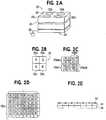
- a conventional camera 10, shown in FIG. 1Aincludes a lens 12 with a focal length f and a detector array 14, having a plurality of pixels.
- a detector array 14having a plurality of pixels.
- An example of the filter array 15is shown in FIG. 1B .
- Each filter in the filter array 15corresponds to a detector, or pixel, in the detector array 14.
- this camerais relatively thick.
- One approach to realizing a thin camera with sufficient resolutioninvolves scaling an imaging system of a conventional camera, e.g., an f/1 camera having a lens with a focal length f.
- the focal planehas n x pixels or sensors of a size p x in the x-direction and n y pixels of size p y in the y-direction.
- the resolutionis then defined as 1/ p x in the x-direction and 1/ p y in the y-direction. If p x and p y could be reduced by a desired scaling factor, thus keeping n x and n y the same, as noted above, then f could be reduced, while maintaining the resolution.
- this scaled down pixel sizemay be limited by availability and/or price of current sensors. Further, there is not enough power in such a scaled down system.
- Another solutionuses compound eye image capturing, the size of the lens being in accordance with a desired thinness of the camera.
- Each lens in the compound eyecorresponds to a plurality of pixels, with the compound eye being selected so that spacing of the lenses is not an integral multiple of pixel spacing.
- each lenslooks at different shifted images.
- the lenses used in the compound eye image capturing systemgenerally have low resolution, for example a PSF equal or larger than the area of each pixel. A resolution greater than that of an individual sub-camera is achieved by combining the images from multiple cameras.
- a color filter array 15' shown in FIG. 1Chas a color filter for each lens. Multiple lenses are used for each color and the images for each color combined.
- the use of compound eye image capturingis computationally intensive and it is difficult to achieve a resolution equal or close to that of the number of pixels in the sensor array for the entire composite image.
- an image sensing apparatuswhich can satisfactorily correct mis-registration among images, and can composite the images.
- an image sensing apparatusincludes: a plurality of apertures that receives external light from different positions: a plurality of image sensing units that outputs image signals obtained by independently receiving light that comes from an identical position of an object and is received via the plurality of apertures, and independently extracting predetermined color components for each received light; and a signal processing device that forms a signal that outputs an object image by mixing the image signals output from the plurality of image sensing units.; When it is determined that a predetermined. position deviation occurs between the image signals upon forming the signal that outputs the object image, the signal processing device corrects the predetermined position deviation. by a signal process, and forms the signal that outputs the object image
- EP1348990 A1discloses an image capturing lens to capture an image of an object provided, the image capturing lens includes an aperture diaphragm having an aperture through which an image is captured; a first lens having a positive refracting power, wherein both surfaces of the first lens are shaped in a convex form: a second lens having a negative refracting power, wherein an object-side surface of the second lens is shaped a concave form; and a third lens which is a meniscus lens whose convex surface faces toward the object side: wherein the aperture diaphragm, the firs lens, the second lens and the third lens are aligned in this order from the object side.
- GB 2320837 Adiscloses a colour filter array and its processing circuit in which a vertical interpolation process is not needed, which can be used in a video camera, digital camera, colour scanner, or colour copier, is constituted such that the number of green colour filters is double the respective numbers of red and blue colour filters in order to make human colour recognition easy.
- the red and blue colour filtersare places every four pixels and a green colour filter is placed every other pixel along each line of the image, for example defining a filter pattern consisting of R-G-B-G, G-R-G-B and B-G-R-G filter groups.
- FIG. 4is a schematic side view of an embodiment of the present invention including a mask adjacent to the lenses;
- FIG. 5Ais a schematic side view of a specific lens system for use with the present invention.
- FIG. 5Bis a schematic perspective view of the lens system of FIG. 7A;
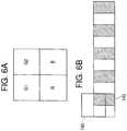
- FIG. 6Ais a schematic top view of a sub-camera arrangement according to an embodiment of the present invention.
- FIG. 6Bis a schematic top view of shifted images for a sub-camera of FIG. 6A .
- a thin camera 20includes an imaging lens array (ILA) 22, a color filter 25 and a detector array 24.
- the detector array 24may be the same is in the conventional camera, and may include a microlens array, with a microlens corresponding to each pixel to improve the fill factor.
- ILAimaging lens array
- Dwhen the focal length of the conventional single lens is halved, D is also halved and the F# is maintained.
- a 2x2 array of lenses 22a-22dcan be used with each lens addressing a quarter of the area of the sensor plane.
- Each combination of a lens 22a-22d, a color filter 25a-25d and corresponding portion of the detector array 24constitutes a sub-camera.
- a sub-camerathere are a total of four sub-cameras.
- the images from each of the four sub-camerasare provided to a processor 30 where they are combined in a known manner to form a composite color image.
- the color filter 25may be placed anywhere between the front of the camera and the sensor plane.
- the number of lenses or sub-cameras in the arrayis driven by a combination of several factors.
- the point spread function (PSF) of the opticsis preferably smaller than the pitch of the pixels on the sensor.
- PSFpoint spread function
- the color filter 25may have a different color filter 25a through 25d corresponding to each lens 22a through 22d, as shown in FIG. 2B .
- filter 25amay transmit red (R) light
- filters 25b and 25cmay transmit green (G) light
- filter 25dmay transmit blue (B) light. Since each lens captures the entire image, a composite image can be realized by combining the images from each sub-camera. The composite image will have higher resolution that that of the individual sub-cameras. For example, in a conventional one megapixel, i.e. one million pixels, camera, there are 250,000 blue pixels, 250,000 red pixels and 500,000 green pixels.
- Each pixelsamples light from a different portion of the image. Yet one million full color pixels are generated, typically by interpolation. If each image on each camera is identical, then there would be 250,000 red pixels of information, 250,000 blue pixels and 500,000 green pixels, 250,000 for each green sub-camera. So, there would be the same number of independent samples of information as in the conventional one megapixel camera for red and blue, but less for green, since the two green sub-cameras would be identical.
- the two green camerasmay be distinguished from one another by placing apertures near the detector plane.
- the two green sub-cameraswill sample different portions of the image and thus generate 500,000 samples of information, rather than 250,000.
- Any method that will allow a different set of samples in the two green camerasachieves this increase.
- Other techniquesinclude generating an image on the sensor plane for one green camera that is shifted slightly with respect to the other green camera, and using a combination of apertures and image shifting.
- CMOS image sensorstypically have embedded circuitry that blocks a significant portion of the light incident on each pixel. For example, 25% -70% of the area of each pixel is typically blocked by this circuitry.
- MLAsmicro-lens arrays
- the pitch of the lenses in the MLAis equal to the pitch of the pixels on the CMOS sensor chip, i.e., there is one micro-lens for each pixel. This approach typically improves the light capture efficiency of each pixel to approximately 75-85%.
- one way to achieve the light blocking aperturesis to simply use the CMOS sensor chips without the micro-lenses, in the sub-cameras containing the green filters.
- the two green cameraswill sample the image in different locations, i.e., different data will be generated by the two green cameras. If the two green camera images do have identical registrations with respect to the pixels, then circuit design can be modified on the image sensor chip so that the circuitry is blocking the light in different regions in the first green sub camera than in the second green sub camera.
- MLAscan be used to shift the portions of the image that is detected by each pixel.
- the MLAscan be designed so that each micro-lens is slightly off-center of the active area of each pixel. In this manner a slightly different portion of the image is focused on to the active area of the sensor for the two green cameras.
- the MLAscan provide one shift for one camera and a different one for another camera.
- each micro-lens within a sub-cameracan provide a slightly different shift for every pixel, ensuring that the majority of the corresponding green pixels in the two green sub cameras receive different signals, for all ranges of object distance within the desired object distance range.
- one sub-camerais red
- one sub-camerais blue
- the other two sub camerasare green.
- the red and blue resolution in the composite imageis therefore the same as in the sub camera.
- the resolution for the composite image for the green coloris increased over that of an individual camera, since information from the two individual cameras is combined to form a higher resolution composite image.
- each lens 22a-22dmay be assigned a different patterned color filter 25aa through 25dd, each lens being associated with a 4x4 color filter array. Since the position of the R and B filters are in different quadrants of the 4x4 array, and each lens captures the entire image, the color image may be realized. Again, there are twice as many G filters, here occupying each quadrant twice.
- a conventional color filter R-G-B color filter patterncan be used in which each pixel has a color filter associated therewith.
- each cameracaptures identical images on the sensor plane, then the locations of the R, G and B filters need to be in different locations, for each camera.
- a quarter of the pixelsgenerate N/4 sampling points of red
- a quarter of the pixelsgenerate N/4 samples of blue in the image
- half of the pixelsgenerate the N/2 samples of green. Any of the methods described above can be used to ensure that the N/2 samples of green are substantially independent.
- each sub-cameraimages only one color.
- for each pixel in the composite imagethere are four corresponding pixel samples, one blue, one red and two green.
- each of these pixel samplesoriginates from a different sub-camera.
- all of the red pixelsoriginate from one sub-camera.
- the red pixel informationis obtained from different sub-cameras for different pixels.
- any of the filters of FIGS. 2B - 2Dmay be combined with a mask for a pixel, as shown in FIG. 2E .
- a maskmay have a plurality n x n y of macro-pixels 34 of size d x d y , with one macro-pixel 34 for each sensor 36.
- Each macro-pixel 34serves as a filter and has a feature 32.
- Each macro-pixelis between the ILA 22 and a detector array 24 (shown in Figure 2A ) including a plurality of sensors 36.
- the macro-pixel size d x d ymay be the same as or greater than the pixel or sensor size p x p y .
- each macro-pixel 34has m micro-pixels 32 of size q. More generally, there are m x micro-pixels 32 of a size q x in the x-direction and m y micro-pixels of size q y in the y-direction.
- the power incident on each sensor 36is equal to a summation, over all micro-pixels 32 on the corresponding macro-pixel 34, of the power on each micro-pixel 32 multiplied by the transmittance of the micro-pixels.
- Each micro-pixelmay 32 either be open or closed, i.e., have a transmission of one or zero, and only one of the m x x m y micro-pixels 32 in each macro-pixel 34 may be open.
- the size of the lensis also 400 microns, e.g., the lens has a 400 micron diameter if it is spherical and a 400 micron width if it is square.
- the cameraSince the camera will be arrayed, it is desirable to limit the sensor elements 36 to within approximately the same dimensions as the lens size, so that there will be no dead space between lenses in the array. That limits the size of the sensor array to approximately 400 microns in diameter, and thus the number of sensors 36 to a 20x20 array. In this case, the resolution of the camera is now equal to 1/q x x 1/q y . However, the result is a sampled image, i.e., the image would contain 20x20 samples of a 200x200 pixel image
- the remaining pixelscan be obtained by forming an array of micro-cameras, each including a micro-lens 22a, a plurality of sensors 36, and a plurality of macro-pixels 34 having a feature 32.
- the number of micro-lenses Imay be different in the x-direction than the y-direction, i.e., l x , l y .
- the macro-pixels 34may be located at an image plane of the micro-camera.
- the number n x , n y of macro-pixels 34 and sensors 36is determined by the selected size p x , p y of the pixel and the size of the image at the image plane.
- All of these elementsmay be unitary devices, with the micro-cameras 30 being defined by individual micro-lenses 22. While the example above has an open micro-pixel of size q for each macro-pixel, as long as there are n x n y sensors for the camera viewing each portion of the image with a filter having a feature with a desired minimum feature size q, the desired resolution may be realized. By combining the above color filter, half of the sub-pixels needed to increase the resolution as discussed above may be needed.
- multiple holes or micro-pixelsmay be open per macro-pixel.
- all of the micro-pixels in the array of micro-pixelsare open, no light is blocked to the macro-pixel. If only one of the micro-pixels is open, the desired resolution is realized on the corresponding macro-pixel.
- the imagecan be decomposed by the micro-cameras in a variety of manners, as long as all of the information for each macro-pixel is captured.
- the ratio of the size of each macro-pixel to the size of each micro-pixelmay be proportional to a number of micro-cameras in the thin camera.
- micro-pixelsmay allow all light in a macro-pixel to pass through, giving an average value of the intensity for that macro-pixel. Typically, most macro-pixels will have at least half of the micro-pixels open. Further, a gray scale approach, where each micro-pixel is assigned a transmittance that may vary between micro-pixels. Then, rather than referring to the micro-pixels as being open and closed, the macro-pixel would receive some level of transmittance. For example, at least 20% of the micro-pixels in a majority of the macro-pixels may have transmittances greater than 0.4
- the backside of the lens arraycould be etched into curved surfaces centered on each lens. Or the back surface could be etched in a series of discrete rings approximating a curved surface. The holes would then be provided on this curved or other non-flat surface. Providing the holes on a curved or other non-flat surface helps insure the image is diffraction limited across a wide field
- FIGS. 3A and 3BOther alternatives for realizing color images are shown in FIGS. 3A and 3B .
- a filter 35would include regions 35a through 35d.
- Region 35atransmits all light, i.e., has no filter
- region 35btransmits red and green
- region 35ctransmits blue and green
- region 35dtransmits red and blue.
- Region 35dmay be eliminated, due to the green dominance realized by the other regions. If all four regions are used, then to determine the value of red simply subtract the power from a pixel in region 35c, from the corresponding pixel in region 35a. Similarly, the values for the other colors can also be obtained.
- FIG. 3BAnother alternate embodiment uses a color filter 37 shown in Fig. 3B , which uses the format established by the Joint Photographic Experts Group (JPEG). Again assuming four lenses are used, the filter 37 would include regions 37a through 37d. As shown in FIG. 3B , two of the regions 35a, 35d have a Y filter, region 35b has a R filter and region 35c has a B filter.
- the YUV componentsmay be determined from the filter 37 shown in FIG. 3B .
- the signal transmitted by the Y filterserves as the luminance. If more of the light needs to be transmitted, the proportions of the light transmitted by the Y filter could remain the same, while passing about all of the green light, about 0.51 of the red light, and about 0.2 of the blue light, with the remaining filters staying the same.
- JPEG encodinghas a higher number of Y samples. This fact may be used to improve the resolution of the camera. For example, by providing different information on the different Y regions, resolution can be improved. Such different information may be provided by blocking some of the light, shifting the image, or a combination thereof. If the point spread function (PSF) of the ILA is smaller than the pixel size, by focusing the light for one of the Y regions onto metal or other opaque material in the plane of the detector array to block some of the light will result in a differences between the images of the two Y regions. This may also be achieved by eliminating the microlens associated with each pixel to receive the altered image.
- PSFpoint spread function
- appropriate lenses in the ILA or microlenses for the detectorsmay be offset, i.e. to be off-axis.
- the resolution of the composite imagewill be determined by that of the Y image, with the other color images having a lower resolution.
- the Y filterallows more power through than the other filters, light can be blocked for this filter while equalizing power on the array of detectors.
- the same approachmay be used with the green filters for the red, blue, green configuration. Further, the shifting and/or blocking may be used in both Y regions. Additionally, the blocking may be realized using the apertures noted above. Finally, relative shifting of the blue and red images to each other may be used to improve the resolution of these images.
- a light blocking element between the lenses themselves or between the lenses and the detector plane isolating light from the respective lensesmay be used to minimize this crosstalk.
- Such a blocking elementmay be opaque or absorptive. These blocking elements may be in addition to or in place of conventional stops within the system. While keeping the same detector size, the lens size may be reduced to maintain the f/#, and the space between the lenses may include a blocking element. The use of smaller lenses with a low fill factor (e.g.
- a mask 68may be provided on this surface, as shown in FIG. 4 .
- the alignment of the lenses 42 and the mask 62may be readily realized, since they are on the same substrate 60.
- An additional substrate 70 including further optical elements 72 for imaging onto the detector plane 44may be used.
- the optical elements 72may be of poor quality, e. g., having aberrations, while collecting all the light.
- the alignment of the mask 68 relative to the lenses 42 on the same substrate 60is much more readily achieved than aligning the mask 68 to the detector plane 44. Further, this reduces the alignment requirements between the lenses 42 and the detector plane 44.
- a specific example of a lens of the ILA to be used with the present inventionis shown in 5A and 5B.
- the different light pathscorrespond to different field points from the object
- a first substrate 110has a first refractive surface 112 which collimates the light input thereto.
- a second surface 114 of the first substratemay be planar and may include an infrared filter 115 thereon.
- a first surface 122 of an intermediate substrate 120may have a diffractive element 123 thereon, which corrects for color and imaging aberrations. If each sub-camera has a single color filer, a single diffractive element 123 may be used for each sub-camera.
- a second surface 124may have a second refractive surface for focuses the light
- a second substrate 130has a refractive, concave surface 132 therein.
- the concave surface 132flattens the field of the image, so that all image points are focused at the same plane 135 to be imaged onto the detector array 24.
- the imaging of the two green sub-camerasshould receive different images, If the object is located at infinity, the zero frequency pixel will be located at the center of each lens.
- the lenses in the ILAmay be shifted relative to one another by an integer number of pixels plus 1/2 a pixel, in other words.
- the focal lengthis 2mm and assuming the pixel pitch x of 10 microns
- the image shift sremains less than one tenth of a pixel for an object distance from infinity to approximately 3 m away.
- the pixel pitch xis reduced to 3 microns, then when the object distance is 3, then s will be one-third of 1/3 of a pixel.
- one way to ensure different images from cameras with the same or similar color filtersis to provide different optical elements in the paths thereof.
- aperturesi.e., light blocking regions in the detector plane
- one method to ensure different signals on the two green sub-cameras G1 and G2is shown in Fig. 6B .
- the G1 sub-camerahas no apertures.
- the MLA for the G1 camerafocuses nearly all the light in the sensor plane incident on a sensor pixel onto the active area of a pixel.
- On the G2 cameraa portion of the light on each pixel is blocked. In the example shown in FIG.
- the light on the left half of each pixelis blocked with an aperture 140.
- aperturesare used on the G2 camera, blocking light directed on to the left side of each pixel in the G2 camera.
- the relative shift in the x-direction of the images on the two sub-cameraswill change.
- increased resolution in the x-directioncan be achieved for any shift in the x-direction, as long as the relative shift is determined.
- the G2 signalFor example, if the signals on the two cameras are aligned, then by subtracting the signal on the G2 camera from that of the G1 camera, one can determine the signal on the left side of each pixel, since the G2 signal itself returns the average value of the right half of each pixel. If the image shifts by 1 ⁇ 2 of a pixel, then the G2 signal will return the left half of each pixel and subtraction will yield the right half of each pixel. If the image shifts by 1 ⁇ 4 of a pixel, then the G2 signal returns a signal at the midway point between the samples of the G1 signals. If the image shifts by % of a pixel then the centers of the G1 and G2 signals are aligned in the x-direction.
- the right 1 ⁇ 4 pixel valuecan be determined.
- each pixel in the G1 and G2 sub-cameraswill be centered at different locations in both the x and y directions. For example, if there are N/4 pixels in the G1 sub-camera and N/4 pixels for the G2 sub-camera, there will by N/2 unique green images.
- Lenses for red and blue cameras R, Bmay be offset along y-direction for the example in FIG. 6A .
- the above problem of different object distances resulting in integer multiple of pixel shiftsmay arise. However, since in general higher resolution is more apparent in green than in red or blue, such decrease in resolution may not be of concern. If it is, then aperture could similarly be employed in either the red or blue sub-camera. Further, the above solution is also applicable when using Y, U, V sub-cameras, discussed above in connection with FIG. 3B .
Landscapes
- Engineering & Computer Science (AREA)
- Multimedia (AREA)
- Signal Processing (AREA)
- Physics & Mathematics (AREA)
- Spectroscopy & Molecular Physics (AREA)
- Human Computer Interaction (AREA)
- General Physics & Mathematics (AREA)
- Optics & Photonics (AREA)
- Color Television Image Signal Generators (AREA)
- Lenses (AREA)
- Studio Devices (AREA)
- Cameras In General (AREA)
Description
- The present invention is directed to a thin camera. More particularly, the present invention is directed to a thin camera using color filters and/or having an increased field of view.
- A
conventional camera 10, shown inFIG. 1A includes alens 12 with a focal length f and adetector array 14, having a plurality of pixels. To realize color imaging, an array offilters 15 having some pattern, typically with more green filters than red or blue filters, is provided. An example of thefilter array 15 is shown inFIG. 1B . Each filter in thefilter array 15 corresponds to a detector, or pixel, in thedetector array 14. However, this camera is relatively thick. - One approach to realizing a thin camera with sufficient resolution involves scaling an imaging system of a conventional camera, e.g., an f/1 camera having a lens with a focal length f. Assume the focal plane has nx pixels or sensors of a size px in the x-direction and ny pixels of size py in the y-direction. The resolution is then defined as 1/ px in the x-direction and 1/ py in the y-direction. If px and py could be reduced by a desired scaling factor, thus keeping nx and ny the same, as noted above, then f could be reduced, while maintaining the resolution. However, this scaled down pixel size may be limited by availability and/or price of current sensors. Further, there is not enough power in such a scaled down system.
- Another solution uses compound eye image capturing, the size of the lens being in accordance with a desired thinness of the camera. Each lens in the compound eye corresponds to a plurality of pixels, with the compound eye being selected so that spacing of the lenses is not an integral multiple of pixel spacing. Thus, each lens looks at different shifted images. The lenses used in the compound eye image capturing system generally have low resolution, for example a PSF equal or larger than the area of each pixel. A resolution greater than that of an individual sub-camera is achieved by combining the images from multiple cameras. For this solution, a color filter array 15' shown in
FIG. 1C , has a color filter for each lens. Multiple lenses are used for each color and the images for each color combined. However, the use of compound eye image capturing is computationally intensive and it is difficult to achieve a resolution equal or close to that of the number of pixels in the sensor array for the entire composite image. US2002/122124 A1 discloses an image sensing apparatus which can satisfactorily correct mis-registration among images, and can composite the images. To achieve this object, an image sensing apparatus includes: a plurality of apertures that receives external light from different positions: a plurality of image sensing units that outputs image signals obtained by independently receiving light that comes from an identical position of an object and is received via the plurality of apertures, and independently extracting predetermined color components for each received light; and a signal processing device that forms a signal that outputs an object image by mixing the image signals output from the plurality of image sensing units.; When it is determined that a predetermined. position deviation occurs between the image signals upon forming the signal that outputs the object image, the signal processing device corrects the predetermined position deviation. by a signal process, and forms the signal that outputs the object imageEP1348990 A1 discloses an image capturing lens to capture an image of an object provided, the image capturing lens includes an aperture diaphragm having an aperture through which an image is captured; a first lens having a positive refracting power, wherein both surfaces of the first lens are shaped in a convex form: a second lens having a negative refracting power, wherein an object-side surface of the second lens is shaped a concave form; and a third lens which is a meniscus lens whose convex surface faces toward the object side: wherein the aperture diaphragm, the firs lens, the second lens and the third lens are aligned in this order from the object side.GB 2320837 A - According to the present invention there is provided a camera according to
claim 1. - The above and other features and advantages of the present invention will become readily apparent to those of skill in the art by describing in detail embodiments thereof with reference to the attached drawings, in which:
FIG. 1A is a schematic side view of an imaging system in a conventional camera;FIG. 1B is a plan view of a conventional color filter array for use with the conventional camera ofFIG. 1A ;FIG. 1C is a plan view of another conventional color filter array;FIG. 2A is a is a schematic perspective view of an imaging system in a camera according to an embodiment of the present invention;FIGS. 2B to 2D are plan views of color filters according to embodiments of the present invention;FIG. 2E is a schematic exploded side view of a macro-pixel/micro-pixel configuration for use in a micro-camera in an embodiment of the present invention;FIGS. 3A and 3B are plan views of further color filters according to other embodiments of the present invention;FIG. 4 is a schematic side view of an embodiment of the present invention including a mask adjacent to the lenses;FIG. 5A is a schematic side view of a specific lens system for use with the present invention;FIG. 5B is a schematic perspective view of the lens system of FIG. 7A;FIG. 6A is a schematic top view of a sub-camera arrangement according to an embodiment of the present invention; andFIG. 6B is a schematic top view of shifted images for a sub-camera ofFIG. 6A .- It will be understood that when a layer is referred to as being "on" another layer or substrate, it may be directly on the other layer or substrate, or intervening layers may also be present. Further, it will be understood that when a layer is referred to as being "under" another layer, it may be directly under, or one or more intervening layers may also be present. In addition, it will also be understood that when a layer is referred to as being "between" two layers, it may be the only layer between the two layers, or one or more intervening layers may also be present. Like numbers refer to like elements throughout.
- A useful parameter in imaging systems is the f/# of the system, where f/# = f/D, where f is the focal length and D is the size of the aperture of the lens. In creating a thinner camera, while keeping the same f/# as for a conventional camera, when f is reduced, a commensurate reduction in D is needed.
- The general structure of a thin camera in accordance with an embodiment of the present invention is shown in
FIG. 2A . Athin camera 20 includes an imaging lens array (ILA) 22, acolor filter 25 and adetector array 24. Thedetector array 24 may be the same is in the conventional camera, and may include a microlens array, with a microlens corresponding to each pixel to improve the fill factor. As shown in the particular example ofFIG. 2A , when the focal length of the conventional single lens is halved, D is also halved and the F# is maintained. In order to maintain the same field of view as in a conventional camera, a 2x2 array oflenses 22a-22d can be used with each lens addressing a quarter of the area of the sensor plane. Each combination of alens 22a-22d, acolor filter 25a-25d and corresponding portion of thedetector array 24 constitutes a sub-camera. Thus, for the embodiment shown inFIG. 2A , there are a total of four sub-cameras. The images from each of the four sub-cameras are provided to aprocessor 30 where they are combined in a known manner to form a composite color image. Thecolor filter 25 may be placed anywhere between the front of the camera and the sensor plane. - Here, rather than being driven only by thinness, the number of lenses or sub-cameras in the array is driven by a combination of several factors. First, the more lenses used, in general, the thinner the camera. However, it is a feature of an embodiment of the present invention is to achieve a resolution in the composite image equal or comparable to the total number of pixels in the image sensor without a great deal of computational signal processing. In order to achieve this, the point spread function (PSF) of the optics is preferably smaller than the pitch of the pixels on the sensor. The more lenses used, the more difficult recovery the full resolution of the sensor becomes. For example, if the sensor contains one million pixels, then the resolution of the image from each sub-camera is 250,000 pixels, assuming a tow by two ILA is used. However, it is a feature of an embodiment of this invention to produce a composite image with a resolution of or near one million, which means increasing the resolution by roughly a factor of four. For the two by two ILA, the size of the lens and the corresponding thickness of the sub-camera is half that of a conventional single lens camera, while being much more computationally straightforward than for a compound eye camera.
- Exemplary embodiments of the
color filter 25 to be used are shown inFIGS. 2B - 2D . Thecolor filter 25 may have adifferent color filter 25a through 25d corresponding to eachlens 22a through 22d, as shown inFIG. 2B . In particular,filter 25a may transmit red (R) light, filters 25b and 25c may transmit green (G) light, andfilter 25d may transmit blue (B) light. Since each lens captures the entire image, a composite image can be realized by combining the images from each sub-camera. The composite image will have higher resolution that that of the individual sub-cameras. For example, in a conventional one megapixel, i.e. one million pixels, camera, there are 250,000 blue pixels, 250,000 red pixels and 500,000 green pixels. Each pixel samples light from a different portion of the image. Yet one million full color pixels are generated, typically by interpolation. If each image on each camera is identical, then there would be 250,000 red pixels of information, 250,000 blue pixels and 500,000 green pixels, 250,000 for each green sub-camera. So, there would be the same number of independent samples of information as in the conventional one megapixel camera for red and blue, but less for green, since the two green sub-cameras would be identical. - In one embodiment of the invention, the two green cameras may be distinguished from one another by placing apertures near the detector plane. By placing the apertures in different locations within the pixel, the two green sub-cameras will sample different portions of the image and thus generate 500,000 samples of information, rather than 250,000. There are several other ways to achieve this increase in information as well. Any method that will allow a different set of samples in the two green cameras achieves this increase. Other techniques include generating an image on the sensor plane for one green camera that is shifted slightly with respect to the other green camera, and using a combination of apertures and image shifting.
- If apertures are to be used, one method of achieving this is to use the natural light blocking layers inherent in typical CMOS image sensors. CMOS image sensors typically have embedded circuitry that blocks a significant portion of the light incident on each pixel. For example, 25% -70% of the area of each pixel is typically blocked by this circuitry. In conventional cameras, micro-lens arrays (MLAs) are typically used to increase the efficiency of light capture by each pixel. In the conventional approach, the pitch of the lenses in the MLA is equal to the pitch of the pixels on the CMOS sensor chip, i.e., there is one micro-lens for each pixel. This approach typically improves the light capture efficiency of each pixel to approximately 75-85%. In accordance with an embodiment of the present invention, one way to achieve the light blocking apertures is to simply use the CMOS sensor chips without the micro-lenses, in the sub-cameras containing the green filters. As long as the two green images do not have identical registrations with respect to the pixels, the two green cameras will sample the image in different locations, i.e., different data will be generated by the two green cameras. If the two green camera images do have identical registrations with respect to the pixels, then circuit design can be modified on the image sensor chip so that the circuitry is blocking the light in different regions in the first green sub camera than in the second green sub camera.
- In addition to using layers integrated on to the CMOS chip to block portions of the light, special MLAs can be used to shift the portions of the image that is detected by each pixel. For example the MLAs can be designed so that each micro-lens is slightly off-center of the active area of each pixel. In this manner a slightly different portion of the image is focused on to the active area of the sensor for the two green cameras.
- Note that the MLAs can provide one shift for one camera and a different one for another camera. Or alternatively, each micro-lens within a sub-camera can provide a slightly different shift for every pixel, ensuring that the majority of the corresponding green pixels in the two green sub cameras receive different signals, for all ranges of object distance within the desired object distance range.
- So the net result, is that four sub-cameras are used, i.e., one sub-camera is red, one sub-camera is blue and the other two sub cameras are green. When the composite image is formed, the red and blue resolution in the composite image is therefore the same as in the sub camera. However, the resolution for the composite image for the green color is increased over that of an individual camera, since information from the two individual cameras is combined to form a higher resolution composite image.
- As mentioned above, there is no need to increase the resolution for the red and blue sub-cameras. Nevertheless, it may still be advantageous in some cases to use apertures and/or image shifting as described above for green, for the red and blue cameras, to, for example, sample the images in slightly different locations for the red and blue sub-cameras.
- Since each lens captures the whole image, these color images may then be combined for full color with twice the resolution of a conventional color filter/pixel arrangement, i.e., simply using a Bayer pattern.
- Alternatively, as shown in
FIG. 2C , eachlens 22a-22d may be assigned a different patterned color filter 25aa through 25dd, each lens being associated with a 4x4 color filter array. Since the position of the R and B filters are in different quadrants of the 4x4 array, and each lens captures the entire image, the color image may be realized. Again, there are twice as many G filters, here occupying each quadrant twice. - As another alternative, shown in
FIG. 2D , a conventional color filter R-G-B color filter pattern can be used in which each pixel has a color filter associated therewith. In this case, if each camera captures identical images on the sensor plane, then the locations of the R, G and B filters need to be in different locations, for each camera. In any of the embodiments set forth inFIGS. 2B-2D , a quarter of the pixels generate N/4 sampling points of red, a quarter of the pixels generate N/4 samples of blue in the image and half of the pixels generate the N/2 samples of green. Any of the methods described above can be used to ensure that the N/2 samples of green are substantially independent. - In the above embodiments, there are still four cameras. In the first embodiment, each sub-camera images only one color. In the other two embodiments , there are multiple color filters for each sub-camera. However, in all the embodiments, for each pixel in the composite image, there are four corresponding pixel samples, one blue, one red and two green. In all of these approaches, each of these pixel samples originates from a different sub-camera. In the first approach all of the red pixels originate from one sub-camera. In the other approaches, the red pixel information is obtained from different sub-cameras for different pixels. One advantage of providing multiple colors for each sub-camera arises when the imaging range is relatively close to the camera, but target range of object distances is fairly large. Depending on the distance of the object from the camera, there will be a slightly different shift of the images on the sensors. There may be some locations of the image where the signals for both of the green cameras are nearly identical for certain regions. If this is the case then obtaining the green images from more cameras can improve the resolution of the image.
- Any of the filters of
FIGS. 2B - 2D may be combined with a mask for a pixel, as shown inFIG. 2E . For example, such a mask may have a plurality nxny of macro-pixels 34 of size dxdy, with one macro-pixel 34 for eachsensor 36. Each macro-pixel 34 serves as a filter and has afeature 32. Each macro-pixel is between theILA 22 and a detector array 24 (shown inFigure 2A ) including a plurality ofsensors 36. The macro-pixel size dxdy may be the same as or greater than the pixel or sensor size pxpy. All or most of the light transmitted through each macro-pixel may be directed on to the corresponding sensor. The transmittance of each macro-pixel may vary across the macro-pixel. This variation in transmittance can be described by dividing the macro-pixel into micro-pixels, the transmittance of each of which may be uniform. Each macro-pixel 34 has m micro-pixels 32 of size q. More generally, there are mx micro-pixels 32 of a size qx in the x-direction and my micro-pixels of size qy in the y-direction. Thus, the power incident on eachsensor 36 is equal to a summation, over all micro-pixels 32 on the correspondingmacro-pixel 34, of the power on each micro-pixel 32 multiplied by the transmittance of the micro-pixels. - Each micro-pixel may 32 either be open or closed, i.e., have a transmission of one or zero, and only one of the mx x my micro-pixels 32 in each macro-pixel 34 may be open. For this case, consider mx = my =10, giving 100
micro-pixels 32 permacro-pixel 34. Also, consider the same sensor size of 20x20 microns as a conventional camera, and a f/1 lens with a 400 micron focal length. Then, the size of the lens is also 400 microns, e.g., the lens has a 400 micron diameter if it is spherical and a 400 micron width if it is square. Since the camera will be arrayed, it is desirable to limit thesensor elements 36 to within approximately the same dimensions as the lens size, so that there will be no dead space between lenses in the array. That limits the size of the sensor array to approximately 400 microns in diameter, and thus the number ofsensors 36 to a 20x20 array. In this case, the resolution of the camera is now equal to 1/qx x 1/qy. However, the result is a sampled image, i.e., the image would contain 20x20 samples of a 200x200 pixel image - The remaining pixels can be obtained by forming an array of micro-cameras, each including a micro-lens 22a, a plurality of
sensors 36, and a plurality of macro-pixels 34 having afeature 32. The number of micro-lenses I may be different in the x-direction than the y-direction, i.e., lx, ly. The macro-pixels 34 may be located at an image plane of the micro-camera. The number nx, ny of macro-pixels 34 andsensors 36 is determined by the selected size px, py of the pixel and the size of the image at the image plane. All of these elements may be unitary devices, with the micro-cameras 30 being defined byindividual micro-lenses 22. While the example above has an open micro-pixel of size q for each macro-pixel, as long as there are nxny sensors for the camera viewing each portion of the image with a filter having a feature with a desired minimum feature size q, the desired resolution may be realized. By combining the above color filter, half of the sub-pixels needed to increase the resolution as discussed above may be needed. - Alternatively to having a single micro-pixel shifted for each macro-pixel, multiple holes or micro-pixels may be open per macro-pixel. As noted above, when all of the micro-pixels in the array of micro-pixels are open, no light is blocked to the macro-pixel. If only one of the micro-pixels is open, the desired resolution is realized on the corresponding macro-pixel. Thus, the image can be decomposed by the micro-cameras in a variety of manners, as long as all of the information for each macro-pixel is captured. The ratio of the size of each macro-pixel to the size of each micro-pixel may be proportional to a number of micro-cameras in the thin camera. Some arrays of micro-pixels may allow all light in a macro-pixel to pass through, giving an average value of the intensity for that macro-pixel. Typically, most macro-pixels will have at least half of the micro-pixels open. Further, a gray scale approach, where each micro-pixel is assigned a transmittance that may vary between micro-pixels. Then, rather than referring to the micro-pixels as being open and closed, the macro-pixel would receive some level of transmittance. For example, at least 20% of the micro-pixels in a majority of the macro-pixels may have transmittances greater than 0.4
- For small f/# lenses, it may be difficult to provide diffraction limited images over the field of view required. In this case it is sometimes easier to focus the light on to a curved surface. In this manner, the backside of the lens array could be etched into curved surfaces centered on each lens. Or the back surface could be etched in a series of discrete rings approximating a curved surface. The holes would then be provided on this curved or other non-flat surface. Providing the holes on a curved or other non-flat surface helps insure the image is diffraction limited across a wide field
- Other alternatives for realizing color images are shown in
FIGS. 3A and 3B . Assuming four lenses are used, afilter 35 would includeregions 35a through 35d. In the embodiment shown inFIG. 3A , at least two colors are provided on each pixel region.Region 35a transmits all light, i.e., has no filter, region 35b transmits red and green,region 35c transmits blue and green, andregion 35d transmits red and blue.Region 35d may be eliminated, due to the green dominance realized by the other regions. If all four regions are used, then to determine the value of red simply subtract the power from a pixel inregion 35c, from the corresponding pixel inregion 35a. Similarly, the values for the other colors can also be obtained. Thus, only three lenses and associated filters are needed to realize full color, while maintaining green dominance. This also increases the amount of light incident on the detector plane. For example, using a conventional filter, 25% of red light, 25% of blue light and 50% of green light is transmitted. With the three filters noted above, approximately 67% of red light, 67% of blue light and 100% of green light is transmitted. If the same amount of power is to be incident on each detector, then some of the light in the most transmissive filter may be blocked to provide the shifting as noted above, while allowing the detectors to have the same gain. - Another alternate embodiment uses a
color filter 37 shown inFig. 3B , which uses the format established by the Joint Photographic Experts Group (JPEG). Again assuming four lenses are used, thefilter 37 would includeregions 37a through 37d. As shown inFIG. 3B , two of theregions region 35c has a B filter. In accordance with the JPEG standard, the YUV filters transmit in accordance with the following equation (1):

filter 37 shown inFIG. 3B . The signal transmitted by the Y filter serves as the luminance. If more of the light needs to be transmitted, the proportions of the light transmitted by the Y filter could remain the same, while passing about all of the green light, about 0.51 of the red light, and about 0.2 of the blue light, with the remaining filters staying the same. - Typically, JPEG encoding has a higher number of Y samples. This fact may be used to improve the resolution of the camera. For example, by providing different information on the different Y regions, resolution can be improved. Such different information may be provided by blocking some of the light, shifting the image, or a combination thereof. If the point spread function (PSF) of the ILA is smaller than the pixel size, by focusing the light for one of the Y regions onto metal or other opaque material in the plane of the detector array to block some of the light will result in a differences between the images of the two Y regions. This may also be achieved by eliminating the microlens associated with each pixel to receive the altered image. To realize a shifted image, appropriate lenses in the ILA or microlenses for the detectors may be offset, i.e. to be off-axis. Thus, the resolution of the composite image will be determined by that of the Y image, with the other color images having a lower resolution. Again, since the Y filter allows more power through than the other filters, light can be blocked for this filter while equalizing power on the array of detectors.
- The same approach may be used with the green filters for the red, blue, green configuration. Further, the shifting and/or blocking may be used in both Y regions. Additionally, the blocking may be realized using the apertures noted above. Finally, relative shifting of the blue and red images to each other may be used to improve the resolution of these images.
- Increasing the number of lenslets in the ILA means that crosstalk becomes more of an issue. A light blocking element between the lenses themselves or between the lenses and the detector plane isolating light from the respective lenses may be used to minimize this crosstalk. Such a blocking element may be opaque or absorptive. These blocking elements may be in addition to or in place of conventional stops within the system. While keeping the same detector size, the lens size may be reduced to maintain the f/#, and the space between the lenses may include a blocking element. The use of smaller lenses with a low fill factor (e.g. sum of the area of the clear apertures of all the lenses less than 70% of the area of the sensor), in addition to reducing the focal length and maintaining the f/# of the system can be used to decrease cross talk, increase the field of view. While the fill factor of the lens array is then less than 100%, the detectors will still have a 100% fill factor.
- In addition to or instead of having another optical element on the opposite surface of the
substrate 60, amask 68, as discussed above, may be provided on this surface, as shown inFIG.4 . The alignment of thelenses 42 and the mask 62 may be readily realized, since they are on thesame substrate 60. Anadditional substrate 70 including furtheroptical elements 72 for imaging onto thedetector plane 44 may be used. Here, since the mask is not between theoptical elements 72 and thedetector plane 44, theoptical elements 72 may be of poor quality, e. g., having aberrations, while collecting all the light. The alignment of themask 68 relative to thelenses 42 on thesame substrate 60 is much more readily achieved than aligning themask 68 to thedetector plane 44. Further, this reduces the alignment requirements between thelenses 42 and thedetector plane 44. - A specific example of a lens of the ILA to be used with the present invention is shown in 5A and 5B. In
FIGS. 5A and 5B , the different light paths correspond to different field points from the object Afirst substrate 110 has a firstrefractive surface 112 which collimates the light input thereto. Asecond surface 114 of the first substrate may be planar and may include aninfrared filter 115 thereon. Afirst surface 122 of anintermediate substrate 120 may have adiffractive element 123 thereon, which corrects for color and imaging aberrations. If each sub-camera has a single color filer, a singlediffractive element 123 may be used for each sub-camera. Asecond surface 124 may have a second refractive surface for focuses the light Asecond substrate 130 has a refractive,concave surface 132 therein. Theconcave surface 132 flattens the field of the image, so that all image points are focused at thesame plane 135 to be imaged onto thedetector array 24. - In the above embodiments, to improve the resolution, the imaging of the two green sub-cameras should receive different images, If the object is located at infinity, the zero frequency pixel will be located at the center of each lens.
Thus, to achieve the desired image shifts, the lenses in the ILA may be shifted relative to one another by an integer number of pixels plus 1/2 a pixel, in other words. The center to center spacing P between adjacent lenses in the ILA would be given by:
- If the object is not located at infinity, then an image pixel located under the center of one of the lenses will not be located under the center of an adjacent lens. Instead, it will be shifted by an amount s, given by:

- Although the images are located in different relative locations on the sub- camera pixels, depending upon the object distance, there is not an issue in terms of combining the wrong pixels when the composite image is generated. A relatively simple image processing algorithm can be used to determine the amount of shift needed to generate correlated images from different sub-cameras. However, at object locations where the image shift is closer to an integer number of pixels, instead of an integer plus ½, such interpolation becomes a problem, since such a shift would result in little or no difference between the images.
- If a wide range of object distances is needed, one way to ensure different images from cameras with the same or similar color filters is to provide different optical elements in the paths thereof. For example, apertures, i.e., light blocking regions in the detector plane, maybe used. For example, one method to ensure different signals on the two green sub-cameras G1 and G2 is shown in
Fig. 6B . In this embodiment, the G1 sub-camera has no apertures. Thus, the MLA for the G1 camera focuses nearly all the light in the sensor plane incident on a sensor pixel onto the active area of a pixel. On the G2 camera, a portion of the light on each pixel is blocked. In the example shown inFIG. 6B , the light on the left half of each pixel is blocked with anaperture 140. In addition, the lens centers of the two G1 and G2 cameras are placed very close to each other in the y-direction. That is the center co-ordinates of the centers of the lenses in the y-direction are offset by a small amount, e.g., by 0.5 pixels, or 1.5 microns for x=3 microns. Since the y-offset is so small, the shift in the image locations in the y-direction will be very small over a very wide range of object distances. For example if the y-offset is 1/3 of a pixel, then from equation (3), as long as R > 4, then the shift s will change by less than 1/12 of a pixel, from R=4 to R=infinity. Thus a shift of a known fraction of a pixel in the y-direction can be maintained for a wide range of object distances, ensuring that the two green cameras sample the image at different y locations. This will ensure an ability to use the two green camera images to increase the resolution in the y-direction. This resultant shift is indicated by apixel 145 in the G2 camera inFIG. 6B . - To also increase the resolution in the x-direction, apertures are used on the G2 camera, blocking light directed on to the left side of each pixel in the G2 camera. As the object distance changes, the relative shift in the x-direction of the images on the two sub-cameras will change. Using apertures on one sub-camera, but not on the other sub-camera, or using different shaped apertures on the two sub-cameras, increased resolution in the x-direction can be achieved for any shift in the x-direction, as long as the relative shift is determined. For example, if the signals on the two cameras are aligned, then by subtracting the signal on the G2 camera from that of the G1 camera, one can determine the signal on the left side of each pixel, since the G2 signal itself returns the average value of the right half of each pixel. If the image shifts by ½ of a pixel, then the G2 signal will return the left half of each pixel and subtraction will yield the right half of each pixel. If the image shifts by ¼ of a pixel, then the G2 signal returns a signal at the midway point between the samples of the G1 signals. If the image shifts by % of a pixel then the centers of the G1 and G2 signals are aligned in the x-direction. However, by subtracting the corresponding G1 and G2 pixels and using interpolation algorithms, again increased resolution can be achieved. For example, for the ith pixel, if the G1 signal is subtracted from the G2 signal, the result is the sum of the left ¼ pixel and right ¼ pixel. By approximating the left ¼ pixel value to be the same as the previous pixel's right ¼ pixel value, or a weighted average sum of its closest neighboring samples, then the right ¼ pixel value can be determined.
- This embodiment ensures that each pixel in the G1 and G2 sub-cameras will be centered at different locations in both the x and y directions. For example, if there are N/4 pixels in the G1 sub-camera and N/4 pixels for the G2 sub-camera, there will by N/2 unique green images. Lenses for red and blue cameras R, B, may be offset along y-direction for the example in
FIG. 6A . The above problem of different object distances resulting in integer multiple of pixel shifts may arise. However, since in general higher resolution is more apparent in green than in red or blue, such decrease in resolution may not be of concern. If it is, then aperture could similarly be employed in either the red or blue sub-camera. Further, the above solution is also applicable when using Y, U, V sub-cameras, discussed above in connection withFIG. 3B .


Claims (1)
- A color camera (20) comprising:
at least three sub-cameras, each sub-camera including:an imaging system including a lens system havinga first substrate (110) having a convex refractive element (112) for collimating light;a second substrate (130) having a concave refractive element (132) for flattening the field of an image; anda separation between the first substrate (110) and the second substrate (130), the separation between the convex refractive element (112) and the concave refractive element (132) including an air gap,a color filter (25), anda portion of a detector array (24), the concave refractive element (132) being closer to the detector array (24) than the convex refractive element (112) andmeans (30) configured for combining images from the at least three sub-cameras to form a composite multi-color image, wherein the at least three sub-cameras include a total number N of portions of said detector array and a total number X of different color sets, wherein a first number of signals of a first color set is less than N/X and a second number of signals of a second color set is greater than N/X, signals of the second color set being output from at least two of the at least three sub-cameras, wherein a resolution of a composite image of the second color set is greater than a resolution of an individual sub-camera and a resolution of the composite image of the first color set is no greater than that of an individual sub-camera.
Priority Applications (1)
| Application Number | Priority Date | Filing Date | Title |
|---|---|---|---|
| EP11153126.5AEP2315448B1 (en) | 2004-01-26 | 2005-01-26 | Thin camera having sub-pixel resolution |
Applications Claiming Priority (4)
| Application Number | Priority Date | Filing Date | Title |
|---|---|---|---|
| US10/763,396US7405761B2 (en) | 2003-10-01 | 2004-01-26 | Thin camera having sub-pixel resolution |
| US56027304P | 2004-04-08 | 2004-04-08 | |
| US10/949,807US7773143B2 (en) | 2004-04-08 | 2004-09-27 | Thin color camera having sub-pixel resolution |
| PCT/US2005/002520WO2005072370A2 (en) | 2004-01-26 | 2005-01-26 | Thin camera having sub-pixel resolution |
Related Child Applications (2)
| Application Number | Title | Priority Date | Filing Date |
|---|---|---|---|
| EP11153126.5ADivisionEP2315448B1 (en) | 2004-01-26 | 2005-01-26 | Thin camera having sub-pixel resolution |
| EP11153126.5ADivision-IntoEP2315448B1 (en) | 2004-01-26 | 2005-01-26 | Thin camera having sub-pixel resolution |
Publications (3)
| Publication Number | Publication Date |
|---|---|
| EP1712087A2 EP1712087A2 (en) | 2006-10-18 |
| EP1712087A4 EP1712087A4 (en) | 2009-12-16 |
| EP1712087B1true EP1712087B1 (en) | 2021-03-10 |
Family
ID=34831225
Family Applications (2)
| Application Number | Title | Priority Date | Filing Date |
|---|---|---|---|
| EP05712116.2AExpired - LifetimeEP1712087B1 (en) | 2004-01-26 | 2005-01-26 | Thin camera having sub-pixel resolution |
| EP11153126.5AExpired - LifetimeEP2315448B1 (en) | 2004-01-26 | 2005-01-26 | Thin camera having sub-pixel resolution |
Family Applications After (1)
| Application Number | Title | Priority Date | Filing Date |
|---|---|---|---|
| EP11153126.5AExpired - LifetimeEP2315448B1 (en) | 2004-01-26 | 2005-01-26 | Thin camera having sub-pixel resolution |
Country Status (5)
| Country | Link |
|---|---|
| EP (2) | EP1712087B1 (en) |
| JP (3) | JP4797151B2 (en) |
| KR (1) | KR101227544B1 (en) |
| CN (1) | CN1934872B (en) |
| WO (1) | WO2005072370A2 (en) |
Families Citing this family (32)
| Publication number | Priority date | Publication date | Assignee | Title |
|---|---|---|---|---|
| JP4673202B2 (en)* | 2005-12-06 | 2011-04-20 | 株式会社リコー | Image input device |
| KR100827242B1 (en)* | 2006-06-26 | 2008-05-07 | 삼성전기주식회사 | Method and apparatus for image processing |
| EP1874034A3 (en)* | 2006-06-26 | 2011-12-21 | Samsung Electro-Mechanics Co., Ltd. | Apparatus and method of recovering high pixel image |
| KR100809277B1 (en) | 2006-07-05 | 2008-03-03 | 삼성전기주식회사 | Camera Module with Array Lens |
| DE602007006494D1 (en) | 2006-08-01 | 2010-06-24 | Panasonic Corp | CAMERA DEVICE, LIQUID LENS AND IMAGE PROCESSING |
| WO2008060630A2 (en)* | 2006-11-17 | 2008-05-22 | Tessera North America, Inc. | Internal noise reducing structures in camera systems employing an optics stack and associated methods |
| TW200937642A (en)* | 2007-12-19 | 2009-09-01 | Heptagon Oy | Wafer stack, integrated optical device and method for fabricating the same |
| JP4413261B2 (en) | 2008-01-10 | 2010-02-10 | シャープ株式会社 | Imaging apparatus and optical axis control method |
| JP2010118818A (en)* | 2008-11-12 | 2010-05-27 | Sharp Corp | Image capturing apparatus |
| TW201109165A (en)* | 2009-09-11 | 2011-03-16 | E Pin Optical Industry Co Ltd | Stacked disk-shaped optical lens array, stacked disk-shaped lens module array and the method of manufacturing thereof |
| EP2518995B1 (en) | 2009-12-24 | 2018-08-22 | Sharp Kabushiki Kaisha | Multocular image pickup apparatus and multocular image pickup method |
| CN103201838A (en)* | 2010-06-14 | 2013-07-10 | 赫普塔冈微光学有限公司 | Method of manufacturing a plurality of optical devices |
| GB2488519A (en) | 2011-02-16 | 2012-09-05 | St Microelectronics Res & Dev | Multi-channel image sensor incorporating lenslet array and overlapping fields of view. |
| WO2012143983A1 (en) | 2011-04-22 | 2012-10-26 | パナソニック株式会社 | Image capture device, imgae capture system, and image capture method |
| US8717483B2 (en) | 2011-04-22 | 2014-05-06 | Panasonic Corporation | Imaging device, imaging system, and imaging method |
| US8866951B2 (en)* | 2011-08-24 | 2014-10-21 | Aptina Imaging Corporation | Super-resolution imaging systems |
| CN102510450A (en)* | 2011-10-17 | 2012-06-20 | 北京瑞澜联合通信技术有限公司 | Image sensor, pick-up device and image data generation method |
| US9191635B2 (en) | 2012-03-19 | 2015-11-17 | Semiconductor Components Industries, Llc | Imaging systems with clear filter pixels |
| US8791403B2 (en)* | 2012-06-01 | 2014-07-29 | Omnivision Technologies, Inc. | Lens array for partitioned image sensor to focus a single image onto N image sensor regions |
| US9595553B2 (en)* | 2012-11-02 | 2017-03-14 | Heptagon Micro Optics Pte. Ltd. | Optical modules including focal length adjustment and fabrication of the optical modules |
| WO2014091706A1 (en)* | 2012-12-14 | 2014-06-19 | コニカミノルタ株式会社 | Image capture device |
| JP6186573B2 (en)* | 2013-08-06 | 2017-08-30 | 株式会社モルフォ | Image processing apparatus and image processing method |
| WO2015041496A1 (en)* | 2013-09-23 | 2015-03-26 | 엘지이노텍 주식회사 | Camera module and manufacturing method for same |
| US10662104B2 (en) | 2014-01-24 | 2020-05-26 | Konica Minolta, Inc. | Method for manufacturing lens array optical system and lens array optical system |
| US9983663B2 (en)* | 2014-05-16 | 2018-05-29 | Qualcomm Incorporated | Imaging arrangement for object motion detection and characterization |
| JP6495774B2 (en)* | 2015-07-23 | 2019-04-03 | 株式会社東芝 | Shape recognition apparatus and method |
| US20190179132A1 (en)* | 2017-12-07 | 2019-06-13 | Lg Electronics Inc. | Electronic device having camera device |
| KR102105467B1 (en)* | 2017-12-07 | 2020-05-29 | 엘지전자 주식회사 | Electronic device having camera device |
| US10616536B2 (en) | 2018-01-12 | 2020-04-07 | Semiconductor Components Industries, Llc | Imaging systems having broadband monochromatic and chromatic image sensors |
| CN109672816B (en)* | 2019-01-04 | 2021-03-09 | 多普光电科技有限公司 | Matrix image acquisition system and matrix image projection system |
| KR102632474B1 (en)* | 2019-02-11 | 2024-02-01 | 삼성전자주식회사 | Pixel array included in image sensor and image sensor including the same |
| US12408459B2 (en) | 2021-11-30 | 2025-09-02 | Visera Technologies Company Limited | Image sensor having liquid-lens units and method for detecting images |
Citations (2)
| Publication number | Priority date | Publication date | Assignee | Title |
|---|---|---|---|---|
| GB2320837A (en)* | 1996-12-30 | 1998-07-01 | Hyundai Electronics Ind | Colour filter array and its interpolation apparatus |
| EP1348990A1 (en)* | 2002-03-25 | 2003-10-01 | Konica Corporation | Objective composed of three aspherical lenses |
Family Cites Families (23)
| Publication number | Priority date | Publication date | Assignee | Title |
|---|---|---|---|---|
| JP2921163B2 (en)* | 1991-04-08 | 1999-07-19 | キヤノン株式会社 | Imaging device having optical low-pass filter |
| JPH06269010A (en)* | 1993-03-13 | 1994-09-22 | Victor Co Of Japan Ltd | Color separation optical system, image pickup method and image pickup device |
| US5757423A (en)* | 1993-10-22 | 1998-05-26 | Canon Kabushiki Kaisha | Image taking apparatus |
| JPH08172635A (en)* | 1994-12-16 | 1996-07-02 | Minolta Co Ltd | Image pickup device |
| US5751492A (en)* | 1996-06-14 | 1998-05-12 | Eastman Kodak Company | Diffractive/Refractive lenslet array incorporating a second aspheric surface |
| US6137535A (en)* | 1996-11-04 | 2000-10-24 | Eastman Kodak Company | Compact digital camera with segmented fields of view |
| US6437925B1 (en)* | 1998-06-30 | 2002-08-20 | Olympus Optical Co., Ltd. | Optical apparatus |
| JP2000260056A (en)* | 1999-01-08 | 2000-09-22 | Asahi Optical Co Ltd | Compound objective lens, spherical aberration correction element and optical information recording / reproducing device |
| US6611289B1 (en)* | 1999-01-15 | 2003-08-26 | Yanbin Yu | Digital cameras using multiple sensors with multiple lenses |
| JP3624112B2 (en)* | 1999-03-02 | 2005-03-02 | 独立行政法人科学技術振興機構 | Auto focus glasses |
| WO2000052511A1 (en)* | 1999-03-03 | 2000-09-08 | Mitsubishi Denki Kabushiki Kaisha | Infrared optical system for infrared camera |
| US6727521B2 (en)* | 2000-09-25 | 2004-04-27 | Foveon, Inc. | Vertical color filter detector group and array |
| JP2001013306A (en)* | 1999-06-28 | 2001-01-19 | Canon Inc | Variable focus lens device |
| US6859229B1 (en)* | 1999-06-30 | 2005-02-22 | Canon Kabushiki Kaisha | Image pickup apparatus |
| US6806988B2 (en)* | 2000-03-03 | 2004-10-19 | Canon Kabushiki Kaisha | Optical apparatus |
| US7262799B2 (en)* | 2000-10-25 | 2007-08-28 | Canon Kabushiki Kaisha | Image sensing apparatus and its control method, control program, and storage medium |
| JP2002135796A (en)* | 2000-10-25 | 2002-05-10 | Canon Inc | Imaging device |
| JP2002252338A (en)* | 2000-12-18 | 2002-09-06 | Canon Inc | Imaging device and imaging system |
| US6635941B2 (en)* | 2001-03-21 | 2003-10-21 | Canon Kabushiki Kaisha | Structure of semiconductor device with improved reliability |
| US7009638B2 (en)* | 2001-05-04 | 2006-03-07 | Vexcel Imaging Gmbh | Self-calibrating, digital, large format camera with single or multiple detector arrays and single or multiple optical systems |
| JP3705766B2 (en)* | 2001-11-28 | 2005-10-12 | 独立行政法人科学技術振興機構 | Image input device |
| JP3567327B2 (en)* | 2002-05-08 | 2004-09-22 | 富士写真光機株式会社 | Imaging lens |
| JP2004088713A (en)* | 2002-06-27 | 2004-03-18 | Olympus Corp | Imaging lens unit and imaging device |
- 2005
- 2005-01-26EPEP05712116.2Apatent/EP1712087B1/ennot_activeExpired - Lifetime
- 2005-01-26CNCN200580008795.XApatent/CN1934872B/ennot_activeExpired - Lifetime
- 2005-01-26WOPCT/US2005/002520patent/WO2005072370A2/enactiveApplication Filing
- 2005-01-26KRKR1020067017082Apatent/KR101227544B1/ennot_activeExpired - Lifetime
- 2005-01-26JPJP2006551449Apatent/JP4797151B2/ennot_activeExpired - Lifetime
- 2005-01-26EPEP11153126.5Apatent/EP2315448B1/ennot_activeExpired - Lifetime
- 2011
- 2011-01-06JPJP2011001385Apatent/JP2011072039A/enactivePending
- 2011-12-07JPJP2011268244Apatent/JP5646445B2/ennot_activeExpired - Lifetime
Patent Citations (2)
| Publication number | Priority date | Publication date | Assignee | Title |
|---|---|---|---|---|
| GB2320837A (en)* | 1996-12-30 | 1998-07-01 | Hyundai Electronics Ind | Colour filter array and its interpolation apparatus |
| EP1348990A1 (en)* | 2002-03-25 | 2003-10-01 | Konica Corporation | Objective composed of three aspherical lenses |
Also Published As
| Publication number | Publication date |
|---|---|
| KR20070019979A (en) | 2007-02-16 |
| JP5646445B2 (en) | 2014-12-24 |
| JP2007520166A (en) | 2007-07-19 |
| CN1934872A (en) | 2007-03-21 |
| EP2315448B1 (en) | 2018-03-07 |
| KR101227544B1 (en) | 2013-01-31 |
| CN1934872B (en) | 2016-08-03 |
| EP1712087A4 (en) | 2009-12-16 |
| JP2012070431A (en) | 2012-04-05 |
| WO2005072370A3 (en) | 2005-12-08 |
| EP2315448A1 (en) | 2011-04-27 |
| JP4797151B2 (en) | 2011-10-19 |
| WO2005072370A2 (en) | 2005-08-11 |
| JP2011072039A (en) | 2011-04-07 |
| EP1712087A2 (en) | 2006-10-18 |
Similar Documents
| Publication | Publication Date | Title |
|---|---|---|
| EP1712087B1 (en) | Thin camera having sub-pixel resolution | |
| US7773143B2 (en) | Thin color camera having sub-pixel resolution | |
| US12133007B2 (en) | Solid-state image pickup device and electronic apparatus | |
| JP5538553B2 (en) | Solid-state imaging device and imaging apparatus | |
| US9490281B2 (en) | Image sensor and image capturing apparatus | |
| US8988582B2 (en) | Multi-channel image sensors | |
| US7483065B2 (en) | Multi-lens imaging systems and methods using optical filters having mosaic patterns | |
| US8325266B2 (en) | Method of forming thin camera | |
| EP2083447A1 (en) | Image pickup apparatus | |
| US20130278802A1 (en) | Exposure timing manipulation in a multi-lens camera | |
| JP2006033493A (en) | Imaging device | |
| KR20070120360A (en) | Camera module | |
| CN103843320B (en) | Image Sensors and Imaging Devices | |
| US20100165156A1 (en) | Image capture device comprising focusing adjustment means | |
| HK1208295A1 (en) | Image processing apparatus, image processing method and image pickup apparatus having the image processing apparatus |
Legal Events
| Date | Code | Title | Description |
|---|---|---|---|
| PUAI | Public reference made under article 153(3) epc to a published international application that has entered the european phase | Free format text:ORIGINAL CODE: 0009012 | |
| 17P | Request for examination filed | Effective date:20060828 | |
| AK | Designated contracting states | Kind code of ref document:A2 Designated state(s):AT BE BG CH CY CZ DE DK EE ES FI FR GB GR HU IE IS IT LI LT LU MC NL PL PT RO SE SI SK TR | |
| DAX | Request for extension of the european patent (deleted) | ||
| RAP1 | Party data changed (applicant data changed or rights of an application transferred) | Owner name:TESSERA NORTH AMERICA, INC. | |
| A4 | Supplementary search report drawn up and despatched | Effective date:20091117 | |
| RIC1 | Information provided on ipc code assigned before grant | Ipc:G11B 7/135 20060101ALI20091111BHEP Ipc:G02B 5/18 20060101AFI20091111BHEP | |
| 17Q | First examination report despatched | Effective date:20100316 | |
| RAP1 | Party data changed (applicant data changed or rights of an application transferred) | Owner name:DIGITALOPTICS CORPORATION EAST | |
| RAP1 | Party data changed (applicant data changed or rights of an application transferred) | Owner name:DIGITALOPTICS CORPORATION | |
| STAA | Information on the status of an ep patent application or granted ep patent | Free format text:STATUS: EXAMINATION IS IN PROGRESS | |
| GRAP | Despatch of communication of intention to grant a patent | Free format text:ORIGINAL CODE: EPIDOSNIGR1 | |
| STAA | Information on the status of an ep patent application or granted ep patent | Free format text:STATUS: GRANT OF PATENT IS INTENDED | |
| INTG | Intention to grant announced | Effective date:20201127 | |
| GRAS | Grant fee paid | Free format text:ORIGINAL CODE: EPIDOSNIGR3 | |
| GRAA | (expected) grant | Free format text:ORIGINAL CODE: 0009210 | |
| STAA | Information on the status of an ep patent application or granted ep patent | Free format text:STATUS: THE PATENT HAS BEEN GRANTED | |
| REG | Reference to a national code | Ref country code:DE Ref legal event code:R081 Ref document number:602005057157 Country of ref document:DE Owner name:DIGITALOPTICS CORP., SAN JOSE, US Free format text:FORMER OWNER: DIGITAL OPTICS CORP., CHARLOTTE, N.C., US | |
| AK | Designated contracting states | Kind code of ref document:B1 Designated state(s):AT BE BG CH CY CZ DE DK EE ES FI FR GB GR HU IE IS IT LI LT LU MC NL PL PT RO SE SI SK TR | |
| REG | Reference to a national code | Ref country code:GB Ref legal event code:FG4D | |
| REG | Reference to a national code | Ref country code:CH Ref legal event code:EP Ref country code:AT Ref legal event code:REF Ref document number:1370453 Country of ref document:AT Kind code of ref document:T Effective date:20210315 | |
| REG | Reference to a national code | Ref country code:IE Ref legal event code:FG4D | |
| REG | Reference to a national code | Ref country code:DE Ref legal event code:R096 Ref document number:602005057157 Country of ref document:DE | |
| REG | Reference to a national code | Ref country code:NL Ref legal event code:FP | |
| REG | Reference to a national code | Ref country code:LT Ref legal event code:MG9D | |
| PG25 | Lapsed in a contracting state [announced via postgrant information from national office to epo] | Ref country code:FI Free format text:LAPSE BECAUSE OF FAILURE TO SUBMIT A TRANSLATION OF THE DESCRIPTION OR TO PAY THE FEE WITHIN THE PRESCRIBED TIME-LIMIT Effective date:20210310 Ref country code:GR Free format text:LAPSE BECAUSE OF FAILURE TO SUBMIT A TRANSLATION OF THE DESCRIPTION OR TO PAY THE FEE WITHIN THE PRESCRIBED TIME-LIMIT Effective date:20210611 Ref country code:LT Free format text:LAPSE BECAUSE OF FAILURE TO SUBMIT A TRANSLATION OF THE DESCRIPTION OR TO PAY THE FEE WITHIN THE PRESCRIBED TIME-LIMIT Effective date:20210310 Ref country code:BG Free format text:LAPSE BECAUSE OF FAILURE TO SUBMIT A TRANSLATION OF THE DESCRIPTION OR TO PAY THE FEE WITHIN THE PRESCRIBED TIME-LIMIT Effective date:20210610 | |
| REG | Reference to a national code | Ref country code:AT Ref legal event code:MK05 Ref document number:1370453 Country of ref document:AT Kind code of ref document:T Effective date:20210310 | |
| PG25 | Lapsed in a contracting state [announced via postgrant information from national office to epo] | Ref country code:SE Free format text:LAPSE BECAUSE OF FAILURE TO SUBMIT A TRANSLATION OF THE DESCRIPTION OR TO PAY THE FEE WITHIN THE PRESCRIBED TIME-LIMIT Effective date:20210310 | |
| PG25 | Lapsed in a contracting state [announced via postgrant information from national office to epo] | Ref country code:AT Free format text:LAPSE BECAUSE OF FAILURE TO SUBMIT A TRANSLATION OF THE DESCRIPTION OR TO PAY THE FEE WITHIN THE PRESCRIBED TIME-LIMIT Effective date:20210310 Ref country code:CZ Free format text:LAPSE BECAUSE OF FAILURE TO SUBMIT A TRANSLATION OF THE DESCRIPTION OR TO PAY THE FEE WITHIN THE PRESCRIBED TIME-LIMIT Effective date:20210310 Ref country code:EE Free format text:LAPSE BECAUSE OF FAILURE TO SUBMIT A TRANSLATION OF THE DESCRIPTION OR TO PAY THE FEE WITHIN THE PRESCRIBED TIME-LIMIT Effective date:20210310 | |
| PG25 | Lapsed in a contracting state [announced via postgrant information from national office to epo] | Ref country code:RO Free format text:LAPSE BECAUSE OF FAILURE TO SUBMIT A TRANSLATION OF THE DESCRIPTION OR TO PAY THE FEE WITHIN THE PRESCRIBED TIME-LIMIT Effective date:20210310 Ref country code:IS Free format text:LAPSE BECAUSE OF FAILURE TO SUBMIT A TRANSLATION OF THE DESCRIPTION OR TO PAY THE FEE WITHIN THE PRESCRIBED TIME-LIMIT Effective date:20210710 Ref country code:PL Free format text:LAPSE BECAUSE OF FAILURE TO SUBMIT A TRANSLATION OF THE DESCRIPTION OR TO PAY THE FEE WITHIN THE PRESCRIBED TIME-LIMIT Effective date:20210310 Ref country code:PT Free format text:LAPSE BECAUSE OF FAILURE TO SUBMIT A TRANSLATION OF THE DESCRIPTION OR TO PAY THE FEE WITHIN THE PRESCRIBED TIME-LIMIT Effective date:20210712 Ref country code:SK Free format text:LAPSE BECAUSE OF FAILURE TO SUBMIT A TRANSLATION OF THE DESCRIPTION OR TO PAY THE FEE WITHIN THE PRESCRIBED TIME-LIMIT Effective date:20210310 Ref country code:ES Free format text:LAPSE BECAUSE OF FAILURE TO SUBMIT A TRANSLATION OF THE DESCRIPTION OR TO PAY THE FEE WITHIN THE PRESCRIBED TIME-LIMIT Effective date:20210310 | |
| REG | Reference to a national code | Ref country code:DE Ref legal event code:R097 Ref document number:602005057157 Country of ref document:DE | |
| PLBE | No opposition filed within time limit | Free format text:ORIGINAL CODE: 0009261 | |
| STAA | Information on the status of an ep patent application or granted ep patent | Free format text:STATUS: NO OPPOSITION FILED WITHIN TIME LIMIT | |
| PG25 | Lapsed in a contracting state [announced via postgrant information from national office to epo] | Ref country code:DK Free format text:LAPSE BECAUSE OF FAILURE TO SUBMIT A TRANSLATION OF THE DESCRIPTION OR TO PAY THE FEE WITHIN THE PRESCRIBED TIME-LIMIT Effective date:20210310 | |
| 26N | No opposition filed | Effective date:20211213 | |
| PG25 | Lapsed in a contracting state [announced via postgrant information from national office to epo] | Ref country code:SI Free format text:LAPSE BECAUSE OF FAILURE TO SUBMIT A TRANSLATION OF THE DESCRIPTION OR TO PAY THE FEE WITHIN THE PRESCRIBED TIME-LIMIT Effective date:20210310 | |
| PG25 | Lapsed in a contracting state [announced via postgrant information from national office to epo] | Ref country code:IT Free format text:LAPSE BECAUSE OF FAILURE TO SUBMIT A TRANSLATION OF THE DESCRIPTION OR TO PAY THE FEE WITHIN THE PRESCRIBED TIME-LIMIT Effective date:20210310 | |
| PG25 | Lapsed in a contracting state [announced via postgrant information from national office to epo] | Ref country code:IS Free format text:LAPSE BECAUSE OF FAILURE TO SUBMIT A TRANSLATION OF THE DESCRIPTION OR TO PAY THE FEE WITHIN THE PRESCRIBED TIME-LIMIT Effective date:20210710 | |
| PG25 | Lapsed in a contracting state [announced via postgrant information from national office to epo] | Ref country code:MC Free format text:LAPSE BECAUSE OF FAILURE TO SUBMIT A TRANSLATION OF THE DESCRIPTION OR TO PAY THE FEE WITHIN THE PRESCRIBED TIME-LIMIT Effective date:20210310 | |
| REG | Reference to a national code | Ref country code:CH Ref legal event code:PL | |
| REG | Reference to a national code | Ref country code:BE Ref legal event code:MM Effective date:20220131 | |
| PG25 | Lapsed in a contracting state [announced via postgrant information from national office to epo] | Ref country code:LU Free format text:LAPSE BECAUSE OF NON-PAYMENT OF DUE FEES Effective date:20220126 | |
| PG25 | Lapsed in a contracting state [announced via postgrant information from national office to epo] | Ref country code:FR Free format text:LAPSE BECAUSE OF NON-PAYMENT OF DUE FEES Effective date:20220131 Ref country code:BE Free format text:LAPSE BECAUSE OF NON-PAYMENT OF DUE FEES Effective date:20220131 | |
| PG25 | Lapsed in a contracting state [announced via postgrant information from national office to epo] | Ref country code:LI Free format text:LAPSE BECAUSE OF NON-PAYMENT OF DUE FEES Effective date:20220131 Ref country code:CH Free format text:LAPSE BECAUSE OF NON-PAYMENT OF DUE FEES Effective date:20220131 | |
| PG25 | Lapsed in a contracting state [announced via postgrant information from national office to epo] | Ref country code:IE Free format text:LAPSE BECAUSE OF NON-PAYMENT OF DUE FEES Effective date:20220126 | |
| P01 | Opt-out of the competence of the unified patent court (upc) registered | Effective date:20230524 | |
| PGFP | Annual fee paid to national office [announced via postgrant information from national office to epo] | Ref country code:NL Payment date:20240125 Year of fee payment:20 | |
| PG25 | Lapsed in a contracting state [announced via postgrant information from national office to epo] | Ref country code:HU Free format text:LAPSE BECAUSE OF FAILURE TO SUBMIT A TRANSLATION OF THE DESCRIPTION OR TO PAY THE FEE WITHIN THE PRESCRIBED TIME-LIMIT; INVALID AB INITIO Effective date:20050126 | |
| PG25 | Lapsed in a contracting state [announced via postgrant information from national office to epo] | Ref country code:CY Free format text:LAPSE BECAUSE OF FAILURE TO SUBMIT A TRANSLATION OF THE DESCRIPTION OR TO PAY THE FEE WITHIN THE PRESCRIBED TIME-LIMIT Effective date:20210310 | |
| PGFP | Annual fee paid to national office [announced via postgrant information from national office to epo] | Ref country code:DE Payment date:20240129 Year of fee payment:20 Ref country code:GB Payment date:20240123 Year of fee payment:20 | |
| PG25 | Lapsed in a contracting state [announced via postgrant information from national office to epo] | Ref country code:TR Free format text:LAPSE BECAUSE OF FAILURE TO SUBMIT A TRANSLATION OF THE DESCRIPTION OR TO PAY THE FEE WITHIN THE PRESCRIBED TIME-LIMIT Effective date:20210310 | |
| P02 | Opt-out of the competence of the unified patent court (upc) changed | Free format text:CASE NUMBER: APP_46251/2024 Effective date:20240809 | |
| REG | Reference to a national code | Ref country code:DE Ref legal event code:R071 Ref document number:602005057157 Country of ref document:DE | |
| REG | Reference to a national code | Ref country code:NL Ref legal event code:MK Effective date:20250125 | |
| REG | Reference to a national code | Ref country code:GB Ref legal event code:PE20 Expiry date:20250125 | |
| PG25 | Lapsed in a contracting state [announced via postgrant information from national office to epo] | Ref country code:GB Free format text:LAPSE BECAUSE OF EXPIRATION OF PROTECTION Effective date:20250125 |