EP1711737B1 - Sealed housing unit for lighting system - Google Patents
Sealed housing unit for lighting systemDownload PDFInfo
- Publication number
- EP1711737B1 EP1711737B1EP05706419.8AEP05706419AEP1711737B1EP 1711737 B1EP1711737 B1EP 1711737B1EP 05706419 AEP05706419 AEP 05706419AEP 1711737 B1EP1711737 B1EP 1711737B1
- Authority
- EP
- European Patent Office
- Prior art keywords
- frame
- thermally conductive
- light
- conductive base
- array
- Prior art date
- Legal status (The legal status is an assumption and is not a legal conclusion. Google has not performed a legal analysis and makes no representation as to the accuracy of the status listed.)
- Expired - Lifetime
Links
- 239000000463materialSubstances0.000claimsdescription17
- XLYOFNOQVPJJNP-UHFFFAOYSA-NwaterSubstancesOXLYOFNOQVPJJNP-UHFFFAOYSA-N0.000claimsdescription16
- 239000002274desiccantSubstances0.000claimsdescription12
- 238000007789sealingMethods0.000claimsdescription12
- 238000000034methodMethods0.000claimsdescription11
- 230000003287optical effectEffects0.000claimsdescription7
- 229920001296polysiloxanePolymers0.000claimsdescription5
- 229920002379silicone rubberPolymers0.000claimsdescription4
- 239000004945silicone rubberSubstances0.000claimsdescription4
- 239000000853adhesiveSubstances0.000claimsdescription3
- 230000001070adhesive effectEffects0.000claimsdescription3
- 239000012528membraneSubstances0.000claimsdescription3
- 125000000484butyl groupChemical group[H]C([*])([H])C([H])([H])C([H])([H])C([H])([H])[H]0.000claimsdescription2
- 239000004519greaseSubstances0.000claimsdescription2
- 239000002184metalSubstances0.000claimsdescription2
- 239000010426asphaltSubstances0.000claims1
- 239000003566sealing materialSubstances0.000claims1
- 239000000565sealantSubstances0.000description9
- 238000004806packaging method and processMethods0.000description6
- 238000012360testing methodMethods0.000description5
- 230000005611electricityEffects0.000description4
- 230000017525heat dissipationEffects0.000description4
- 238000004519manufacturing processMethods0.000description4
- 239000004033plasticSubstances0.000description4
- 230000005855radiationEffects0.000description4
- 229920005549butyl rubberPolymers0.000description3
- 239000002826coolantSubstances0.000description3
- 238000002474experimental methodMethods0.000description3
- 239000011521glassSubstances0.000description3
- 238000005286illuminationMethods0.000description3
- 230000035515penetrationEffects0.000description3
- 239000004065semiconductorSubstances0.000description3
- 239000000758substrateSubstances0.000description3
- 230000002411adverseEffects0.000description2
- 230000002860competitive effectEffects0.000description2
- 238000013461designMethods0.000description2
- 230000000694effectsEffects0.000description2
- 239000012780transparent materialSubstances0.000description2
- RICKKZXCGCSLIU-UHFFFAOYSA-N2-[2-[carboxymethyl-[[3-hydroxy-5-(hydroxymethyl)-2-methylpyridin-4-yl]methyl]amino]ethyl-[[3-hydroxy-5-(hydroxymethyl)-2-methylpyridin-4-yl]methyl]amino]acetic acidChemical compoundCC1=NC=C(CO)C(CN(CCN(CC(O)=O)CC=2C(=C(C)N=CC=2CO)O)CC(O)=O)=C1ORICKKZXCGCSLIU-UHFFFAOYSA-N0.000description1
- 239000004593EpoxySubstances0.000description1
- 238000003491arrayMethods0.000description1
- 230000000712assemblyEffects0.000description1
- 238000000429assemblyMethods0.000description1
- 230000004888barrier functionEffects0.000description1
- 230000005540biological transmissionEffects0.000description1
- 239000004020conductorSubstances0.000description1
- 238000001816coolingMethods0.000description1
- 230000002939deleterious effectEffects0.000description1
- 238000011161developmentMethods0.000description1
- 239000000428dustSubstances0.000description1
- 230000005670electromagnetic radiationEffects0.000description1
- 238000011156evaluationMethods0.000description1
- 230000005284excitationEffects0.000description1
- 239000003000extruded plasticSubstances0.000description1
- 239000012530fluidSubstances0.000description1
- 230000007257malfunctionEffects0.000description1
- 230000000116mitigating effectEffects0.000description1
- 238000013021overheatingMethods0.000description1
- 239000012466permeateSubstances0.000description1
- 229920000642polymerPolymers0.000description1
- 239000000047productSubstances0.000description1
- 238000000926separation methodMethods0.000description1
- 125000006850spacer groupChemical group0.000description1
- 238000001228spectrumMethods0.000description1
- 238000012546transferMethods0.000description1
- 238000009423ventilationMethods0.000description1
Images


Classifications
- F—MECHANICAL ENGINEERING; LIGHTING; HEATING; WEAPONS; BLASTING
- F21—LIGHTING
- F21K—NON-ELECTRIC LIGHT SOURCES USING LUMINESCENCE; LIGHT SOURCES USING ELECTROCHEMILUMINESCENCE; LIGHT SOURCES USING CHARGES OF COMBUSTIBLE MATERIAL; LIGHT SOURCES USING SEMICONDUCTOR DEVICES AS LIGHT-GENERATING ELEMENTS; LIGHT SOURCES NOT OTHERWISE PROVIDED FOR
- F21K9/00—Light sources using semiconductor devices as light-generating elements, e.g. using light-emitting diodes [LED] or lasers
- F—MECHANICAL ENGINEERING; LIGHTING; HEATING; WEAPONS; BLASTING
- F21—LIGHTING
- F21V—FUNCTIONAL FEATURES OR DETAILS OF LIGHTING DEVICES OR SYSTEMS THEREOF; STRUCTURAL COMBINATIONS OF LIGHTING DEVICES WITH OTHER ARTICLES, NOT OTHERWISE PROVIDED FOR
- F21V29/00—Protecting lighting devices from thermal damage; Cooling or heating arrangements specially adapted for lighting devices or systems
- F21V29/50—Cooling arrangements
- F21V29/70—Cooling arrangements characterised by passive heat-dissipating elements, e.g. heat-sinks
- F—MECHANICAL ENGINEERING; LIGHTING; HEATING; WEAPONS; BLASTING
- F21—LIGHTING
- F21S—NON-PORTABLE LIGHTING DEVICES; SYSTEMS THEREOF; VEHICLE LIGHTING DEVICES SPECIALLY ADAPTED FOR VEHICLE EXTERIORS
- F21S4/00—Lighting devices or systems using a string or strip of light sources
- F21S4/20—Lighting devices or systems using a string or strip of light sources with light sources held by or within elongate supports
- F21S4/28—Lighting devices or systems using a string or strip of light sources with light sources held by or within elongate supports rigid, e.g. LED bars
- F—MECHANICAL ENGINEERING; LIGHTING; HEATING; WEAPONS; BLASTING
- F21—LIGHTING
- F21S—NON-PORTABLE LIGHTING DEVICES; SYSTEMS THEREOF; VEHICLE LIGHTING DEVICES SPECIALLY ADAPTED FOR VEHICLE EXTERIORS
- F21S8/00—Lighting devices intended for fixed installation
- F21S8/03—Lighting devices intended for fixed installation of surface-mounted type
- F21S8/032—Lighting devices intended for fixed installation of surface-mounted type the surface being a floor or like ground surface, e.g. pavement
- F—MECHANICAL ENGINEERING; LIGHTING; HEATING; WEAPONS; BLASTING
- F21—LIGHTING
- F21V—FUNCTIONAL FEATURES OR DETAILS OF LIGHTING DEVICES OR SYSTEMS THEREOF; STRUCTURAL COMBINATIONS OF LIGHTING DEVICES WITH OTHER ARTICLES, NOT OTHERWISE PROVIDED FOR
- F21V15/00—Protecting lighting devices from damage
- F21V15/01—Housings, e.g. material or assembling of housing parts
- F21V15/013—Housings, e.g. material or assembling of housing parts the housing being an extrusion
- F—MECHANICAL ENGINEERING; LIGHTING; HEATING; WEAPONS; BLASTING
- F21—LIGHTING
- F21V—FUNCTIONAL FEATURES OR DETAILS OF LIGHTING DEVICES OR SYSTEMS THEREOF; STRUCTURAL COMBINATIONS OF LIGHTING DEVICES WITH OTHER ARTICLES, NOT OTHERWISE PROVIDED FOR
- F21V29/00—Protecting lighting devices from thermal damage; Cooling or heating arrangements specially adapted for lighting devices or systems
- F21V29/50—Cooling arrangements
- F21V29/70—Cooling arrangements characterised by passive heat-dissipating elements, e.g. heat-sinks
- F21V29/83—Cooling arrangements characterised by passive heat-dissipating elements, e.g. heat-sinks the elements having apertures, ducts or channels, e.g. heat radiation holes
- F—MECHANICAL ENGINEERING; LIGHTING; HEATING; WEAPONS; BLASTING
- F21—LIGHTING
- F21V—FUNCTIONAL FEATURES OR DETAILS OF LIGHTING DEVICES OR SYSTEMS THEREOF; STRUCTURAL COMBINATIONS OF LIGHTING DEVICES WITH OTHER ARTICLES, NOT OTHERWISE PROVIDED FOR
- F21V31/00—Gas-tight or water-tight arrangements
- F—MECHANICAL ENGINEERING; LIGHTING; HEATING; WEAPONS; BLASTING
- F21—LIGHTING
- F21V—FUNCTIONAL FEATURES OR DETAILS OF LIGHTING DEVICES OR SYSTEMS THEREOF; STRUCTURAL COMBINATIONS OF LIGHTING DEVICES WITH OTHER ARTICLES, NOT OTHERWISE PROVIDED FOR
- F21V31/00—Gas-tight or water-tight arrangements
- F21V31/03—Gas-tight or water-tight arrangements with provision for venting
- H—ELECTRICITY
- H05—ELECTRIC TECHNIQUES NOT OTHERWISE PROVIDED FOR
- H05K—PRINTED CIRCUITS; CASINGS OR CONSTRUCTIONAL DETAILS OF ELECTRIC APPARATUS; MANUFACTURE OF ASSEMBLAGES OF ELECTRICAL COMPONENTS
- H05K5/00—Casings, cabinets or drawers for electric apparatus
- H05K5/02—Details
- H05K5/0213—Venting apertures; Constructional details thereof
- H05K5/0215—Venting apertures; Constructional details thereof with semi-permeable membranes attached to casings
- F—MECHANICAL ENGINEERING; LIGHTING; HEATING; WEAPONS; BLASTING
- F21—LIGHTING
- F21V—FUNCTIONAL FEATURES OR DETAILS OF LIGHTING DEVICES OR SYSTEMS THEREOF; STRUCTURAL COMBINATIONS OF LIGHTING DEVICES WITH OTHER ARTICLES, NOT OTHERWISE PROVIDED FOR
- F21V27/00—Cable-stowing arrangements structurally associated with lighting devices, e.g. reels
- F21V27/02—Cable inlets
- F—MECHANICAL ENGINEERING; LIGHTING; HEATING; WEAPONS; BLASTING
- F21—LIGHTING
- F21W—INDEXING SCHEME ASSOCIATED WITH SUBCLASSES F21K, F21L, F21S and F21V, RELATING TO USES OR APPLICATIONS OF LIGHTING DEVICES OR SYSTEMS
- F21W2131/00—Use or application of lighting devices or systems not provided for in codes F21W2102/00-F21W2121/00
- F21W2131/10—Outdoor lighting
- F—MECHANICAL ENGINEERING; LIGHTING; HEATING; WEAPONS; BLASTING
- F21—LIGHTING
- F21Y—INDEXING SCHEME ASSOCIATED WITH SUBCLASSES F21K, F21L, F21S and F21V, RELATING TO THE FORM OR THE KIND OF THE LIGHT SOURCES OR OF THE COLOUR OF THE LIGHT EMITTED
- F21Y2115/00—Light-generating elements of semiconductor light sources
- F21Y2115/10—Light-emitting diodes [LED]
Definitions
- the present inventionpertains to the field of lighting and in particular to a sealed light-emitting element housing unit.
- LEDs and OLEDshave made these solid-state devices suitable for use in general illumination applications, including architectural, entertainment, and roadway lighting, for example. Due to their ruggedness, low power requirements, and long life, these devices are becoming increasingly competitive with light sources such as incandescent, fluorescent, and high-intensity discharge lamps.
- LED packaginginclude a lead frame that holds the chip and extends to provide an electrical connection.
- the chipcan then be encapsulated in an epoxy plastic package that may be coloured or shaped.
- LED packagingsare tailored for surface mounting the LEDs onto a printed circuit board (PCB) such as disclosed in US Patent No. 4,781,960 , where the LED is mounted in an insulating housing secured by a pair of legs with relatively broad feet which are soldered to conductive pads on the surface of a PCB.
- the leads of the LEDare spot welded to the legs to make electrical connections between the LED and the circuit board.
- Electronic devicessuch as LEDs, however are susceptible to moisture which can interact with the LED die materials and can destroy or cause malfunction of the devices.
- the LED display panel structurecomprises a PCB, a front plate having a plurality of through-holes defined therein, a plurality of washers, each of which is provided on a back surface of the front plate in correspondence with each of the through-holes, a plurality of LEDs, each of which is inserted through a central aperture and each of the washers being smaller than a diameter of the LED to be clamped therein.
- each of whichhas a first recess and a second recess, such that each of the holders receives and holds each of the LEDs in its first recess and is attached on the PCB by water resistant adhesive filled in the second recess.
- a pair of through-bores between the first recess with the second recessreceives a pair of leads which connect each LED to the PCB. In this manner, the circuitry of the LEDs and PCB are protected from moisture.
- This designis specific to a particular and outdated LED packaging and may not be as effective for use with contemporary LEDs and their associated packaging.
- US Patent Nos. 5,927,845 , 5,848,837 and 6,673,292all define various forms of an integral single piece extruded LED light strip and an associated process for producing such an LED light strip.
- the light stripincludes first and second bus elements spaced apart from one another by a predetermined distance.
- the light stripalso includes at least one LED connected between the first and second bus elements and is illuminated when the first bus element conducts electricity provided from a power source.
- An extruded plastic materialcompletely encapsulates the first and second bus elements and the LED, and provides a barrier that protects the elements from damage and makes the light strip impermeable to moisture. This solution, however is more specific to linear LED strips and as such is not suitable for planar LED configurations.
- Canadian Patent Application No. 2,342,267describes an electrically driven light emitting diode (LED) assembly comprising a light emitting diode, first and second electrical leads for conducting electricity to and from the light emitting diode, and a heat sink.
- the assemblyis characterized by the first lead including the heat sink for conducting electricity and heat from the light emitting diode through the heat sink.
- the diodeconducts electricity through a heat sink allowing the diode to be in electrical conductivity with the heat sink.
- the components of the assemblyare enclosed by a transparent or translucent cover.
- a light emitting diodeincludes a heat dissipation structure characterized by having a heat dissipating fluidic coolant filled in a hermetically sealed housing where at least one LED chip mounted on a metallic substrate is dwelled inside.
- the heat dissipation structureis configured with a metallic wall erected from the metallic substrate, which is used to hold a transparent cap of the sealed housing in correct position.
- the erected wallsurrounds in proximity with the at least one LED chip, so that the joule heat generated therefrom can be quickly spread out, through the heat dissipating fluidic coolant, to the erected wall, and then diffused along the wall down to the metallic substrate which adjoins with a larger external heat sink for draining the heat, thus preventing the at least one LED from overheating.
- the transparent cap of the sealed housingis made of transparent materials, wherein a convex portion contacted with the heat dissipating fluidic coolant is formed on the inner surface of the transparent cap.
- WO 2004/107461describes a housing unit for a lighting system comprising a light emitting diode package having at least two heat sinks.
- the light emitting diode packageincludes a main body, at least two lead terminals fixed to the main body, and at least two heat sinks of electrically and thermally conductive materials, the heat sinks being fixed to the main body.
- the at least two heat sinksare separated from each other.
- high luminous powercan be obtained mounting a plurality of light emitting diode dies in one LED package.
- a lensis attached to the main body to enclose the LED dies.
- An object of the present inventionis to provide a sealed housing unit for lighting system.
- a sealed housing unit for a lighting systemcomprising: a thermally conductive base and an array of light-emitting elements in thermal contact with the thermally conductive base, wherein the sealed housing unit further comprises: (a) a frame sealingly connected to the thermally conductive base, wherein said frame is hollow and has an interior surface which includes a means for allowing ingress of water or water vapour into the frame, and wherein the array of light emitting elements is surrounded by the frame and the interior surface of the frame faces the array; (b) an optically transmissive panel sealingly connected to the frame; (c) sealing means associated with the thermally conductive base, the frame and the transmissive panel forming a sealed housing unit enclosing the array of light-emitting elements; and (d) a desiccant or hygroscopic material placed within the frame; wherein said light-emitting elements
- a method for assembling a sealed housing unit for a lighting systemcomprising the steps of: connecting an array of light-emitting elements to a thermally conductive base, connecting a frame to the thermally conductive base, wherein the frame surrounds the array, wherein the frame is hollow and has a desiccant or hygroscopic material therein, the frame having an interior surface which includes a means for allowing ingress of water or water vapour into the frame and the interior surface of the frame facing the array; providing electrical connection to the array of light-emitting elements through at least one sealing aperture in the thermally conductive base or frame , and sealingly connecting an optically transmissive panel to the frame; whereby the frame is sealingly connected to the thermally conductive base and the optically transmissive panel to form a sealed housing unit enclosing the array of light-emitting elements.
- light-emitting elementis used to define any device that emits radiation in the visible region of the electromagnetic spectrum when a potential difference is applied across it or a current is passed through it, for example, a semiconductor, organic or polymer light-emitting diode (LED, OLED or PLED, respectively) or other similar devices as would be readily understood. It would be obvious to one skilled in the art that elements that emit other forms of radiation such as infrared or ultraviolet radiation may also be used if desired in the present invention in place of or in combination with light-emitting elements.
- LEDorganic or polymer light-emitting diode
- diffuseris used to define a device that scatters incident electromagnetic radiation, including visible light, infrared and ultraviolet radiation by means of diffuse transmission, refraction or reflection into a variety of irradiance distribution patterns.
- arrayis used to define a linear 1D or planar 2D arrangement of one or more light-emitting elements.
- Examples of the present inventionprovide a sealed housing unit and a method for its manufacture, wherein the sealed housing unit can protect light-emitting elements and the connected electronic circuitry from moisture.
- the sealed housing unitcomprises a thermally conductive base onto which an array of light-emitting elements is mounted.
- a frameis sealingly connected to the thermally conductive base circumferentially enclosing the array of light-emitting elements and connected circuitry.
- An optically transmissive panelsufficiently sized to span the area defined by the frame, is sealingly connected to the frame to form a sealed cavity enclosing the array of light-emitting elements and the connected circuitry.
- the light-emitting elementscan be electrically activated via electrical wires provided through one or more apertures within the thermally conductive base or the frame. Each aperture comprises a form of sealing means which suppresses the penetration of moisture, dust or other deleterious ingress.
- FIG. 1illustrates an embodiment of the present invention that provides a sealed housing unit for enclosing an array of light-emitting elements.
- the sealed housing unitcomprises a thermally conductive base 10 which acts as a heat sink, wherein an array of LEDs 11 is mounted onto the thermally conductive base 10.
- the LEDsare connected to wires of a cable 12 which passes through a fitting in the thermally conductive base and the cable is connected to an external power supply.
- a frameis sealingly connected to the thermally conductive base surrounding the array of light-emitting elements and their related circuitry providing a separation distance between the thermally conductive base and a transmissive panel connected to the frame.
- the transmissive panelcan be made of glass, plastic or other material as would be readily understood, and that can be sealingly connected to the frame resulting in a sealed unit enclosing the light-emitting elements and the connected circuitry.
- Figure 2illustrates one embodiment of the present invention wherein an array of LEDs 11 is mounted to a thermally conductive base 10.
- the thermally conductive basecomprises an area to which the array of light-emitting elements can be mounted and it provides at least a first side to the sealed housing unit.
- the thermal conductivity of the baseis required to conduct heat generated by the light-emitting elements during operation to a region outside of the sealed housing unit.
- the thermally conductive basecan be formed into a heat sink or can be interconnected to a secondary heat dissipation system, for example a fluid cooling environment, enabling the transfer of heat away from the array of light-emitting elements.
- Other forms of heat removal apparatuscan be interconnected with the thermally conductive base as would be readily understood by a worker skilled in the art.
- the frameis sealingly connected to the thermally conductive base and provides a means for defining a space of sufficient height to enclose the light-emitting elements and their associated packaging within an enclosure defined by the thermally conductive base, the frame and the transmissive panel.
- the framecan comprise two segments sealingly connected to the thermally conductive base along the long axis of the array and the ends of the array can be filled with an appropriate sealant rather than further providing a frame segment along the short axis of the array.
- the framecan fully surround the array of light-emitting elements.
- the shape of the framecan be any desired shape, size and material provided that the frame defines an area sufficient to enclose the desired array of light-emitting elements and the respective circuitry.
- the framecan be a protruding rim or any other integrally formed portion of the thermally conductive base.
- a desiccant or other hygroscopic materialis provided within the inside of the interior space defined by the frame, the transmissive panel and the thermally conductive base.
- the face of the frame facing the interior spacecan have perforations or other porosities or openings or a moisture permeable membrane through which moisture can permeate into the frame that contains or integrally includes desiccant or other hygroscopic material.
- a desiccant or other hygroscopic materialhas a high affinity for water and as such may be used as a drying agent and thereby can reduce any adverse water damage due to water penetration into the sealed housing unit or residual water present during fabrication.
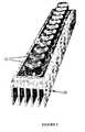
- FIG. 3illustrates one embodiment of the present invention wherein the frame is fabricated from a frame of desiccant filled segments 31 , wherein the face of the frame facing the interior space of the sealed housing unit is perforated for water penetration.
- additional interior spacing elements in the form of spacer barscan be positioned within the array of light-emitting elements in order to provide structural support to the transmissive panel, for example.
- the two internal faces of the additional interior spacing elementsmay be perforated or comprise openings having a moisture permeable membrane associated therewith when these additional spacing elements comprise desiccant or other hygroscopic material therein.
- These interior spacing elementsmay be interconnected to one or both of the transmissive panel and the thermally conductive base, however, this connection may not be required to be a sealed connection. Additionally, if the interior spacing elements are interconnected to both the thermally conductive base and the transmissive panel, this connection should be flexible in order to account for differential thermal expansion, as would be readily understood.
- the transmissive panelcan be an optically clear or diffuse transparent material including glass or plastic or any other suitable material or combination of materials.
- the panelcan additionally be a diffuser or further comprise one or more integrated optics, for example Fresnel or lenticular lenses for manipulating the light originating from the light-emitting elements.
- the panelcan be flat or curved provided that it is able to form a sealed connection with the frame.
- one or more optical elementsare additionally connected to the thermally conductive base proximate to one or more of the light-emitting elements in order to provide a means for optically manipulating the illumination generated by the one or more of the light-emitting elements.
- the space defined by the thermally conductive base, the transmissive panel and the frameis sufficient to enclose the one or more desired optical elements.
- These optical elementcan be for example, reflectors of any of a variety of shapes, collectors or other optical element as would be known to a worker skilled in the art.
- a sealantis used to sealingly interconnect the thermally conductive base, the transmissive panel and the frame and any open regions between the transmissive panel and the base in order to form the desired sealed interior space.
- the sealantcan comprise hot fusible butyl rubber, silicone, silicone rubber or any other known sealant as would be readily understood by a worker skilled in the art.
- the combination of employed sealantscan be defined by factors such as required flexibility and deformability, thereby mitigating the risk of sealing failure due to differential thermal strain between the transmissive panel and the thermally conductive base, for example.
- the light-emitting elementscan be individually mounted on the thermally conductive base or may be mounted on a circuit carrier such as a printed circuit board (PCB) or metal core PCB which is mounted onto the thermally conductive base and both of these configurations are to be considered within the scope of the present invention.
- the thermal contact between the circuit carrier and the thermally conductive basecan be enhanced through the use of a thermally conductive adhesive or thermal grease or other material as would be readily understood by a worker skilled in the art.
- Figure 5illustrates another embodiment of a sealed housing unit in a cut-away view which shows parts of the interior of the unit.
- the unitcomprises light-emitting elements 511 which are aligned in a one dimensional array and are in thermal contact with and mounted onto a circuit carrier 515 which is mechanically and thermally connected to a thermally conductive extruded profile or base 510 .
- the light-emitting elementsare aligned within an optical element 540 which can modify the light emitted by the light-emitting elements under operational conditions to help achieve a desired light output.
- the extruded profilehas a protruding rim along its long axis which provides part of the enclosing frame for the array of light-emitting elements.
- a butyl tape 525 or other sealantis situated between the transparent panel 505 and the edge of the rim to attach and seal a connection.
- the exterior of this connection 520can be further secured and covered with silicone or silicone rubber, for example.
- a glass or plastic element 530covers the end of the unit which is attached and secured by silicone or silicone rubber 521 .
- the opposite end of the unit, which is not shown,can be covered in the same or a similar fashion.
- one or more ventilation apertures 501 as shown in Figure 5can provide for air flow through the side of the extruded profile in order to aid with heat dissipation for example, however this aperture is positioned outside of the enclosure formed with the thermally conductive extruded profile and the transmissive panel.
- the sealed housing unitcan be manufactured by mounting the array of light-emitting elements onto the thermally conductive base wherein they may be wired for external excitation through an aperture through the thermally conductive base or the frame, with the aperture being associated with an appropriate sealing fitting for example.
- a frame of sufficient heightis positioned around the array of light-emitting elements to maintain a preferred distance between the thermally conductive base and the transmissive panel in order create a space to house the light-emitting elements and their associated packaging.
- a sealantsuch as butyl rubber may be used to bond and position the frame on the thermally conductive base.
- this framemay also comprise additional interior elements within the array of light-emitting elements thereby providing additional structural strength to the panel placed on top of the frame for example.
- the transmissive panel of transparent or diffuse materialis subsequently positioned on top of the frame and a sealant such as butyl rubber may be used to bond and position the panel on the frame.
- a sealantsuch as butyl rubber
- silicone or another sealantas would be readily understood, is applied along the edges and interconnection locations between the thermally conductive base, the frame and the transmissive panel thereby bonding and sealing these elements into a single sealed housing unit.
- This sealed housing unit for light-emitting elementscan be more cost effective and simpler to manufacture compared with other sealed housing designs and can be integrated into a variety of lighting products including linear and planar arrays of light-emitting elements. Furthermore, this assembly is amenable to being built on existing automated equipment as would commonly be used to make double glazed window assemblies, for example.
- Table 1illustrates the parameters used for a temperature test performed on a sealed housing unit according to the present invention in order to evaluate the unit integrity while evaluating the temperature of the unit in an enclosed area of controlled temperature.
- This testfurther enabled the evaluation of the effects of differential expansion between the thermally conductive base and the transmissive panel, through paying particular attention to the integrity of the seals during testing.
- the tested sealed housing unitwas a five-foot cove lighting unit with a thermally conductive base designed as a heat sink, the array of light-emitting elements is a linear array of LEDs.
- Figure 6graphically illustrates the positions of each of the temperature sensors collecting information during this experiment.
- the sealed housing unit 52was placed in a cardboard box 53 , which was sealed with the exception of a small vent hole 54 at one end and having an opening at another end for the positioning of the external heat source 51, for example a heat gun, wherein the external heat source was used to raise the ambient temperature inside the box 53. While the sealed housing unit was operational and producing illumination, temperature readings were taken at 15 minute intervals at the five different locations illustrated in Figure 6 . Two temperature readings, T A1 55 and T A2 58, were taken at the two positions in the cardboard box which are indicated in Figure 6 and were used to provide a measure of the ambient temperature.
- T HS 57was taken at the surface of the LED housing unit and fourth and fifth readings, T L1 56 and T L2 59, were taken at two positions within the sealed housing unit, as illustrated in Figure 6 .
- the internal temperature within the sealed housing unitreached a maximum of 84°C and the LEDs were still fully operational.
- the integrity of the seals enclosing and sealing the heat sink, frame and the transmissive panel together to form the sealed housing unitwere still intact.
Landscapes
- Engineering & Computer Science (AREA)
- General Engineering & Computer Science (AREA)
- Microelectronics & Electronic Packaging (AREA)
- Physics & Mathematics (AREA)
- Optics & Photonics (AREA)
- Arrangement Of Elements, Cooling, Sealing, Or The Like Of Lighting Devices (AREA)
- Electroluminescent Light Sources (AREA)
- Led Device Packages (AREA)
Description
- The present invention pertains to the field of lighting and in particular to a sealed light-emitting element housing unit.
- Recent advances in the development of semiconductor and organic light-emitting diodes (LEDs and OLEDs) have made these solid-state devices suitable for use in general illumination applications, including architectural, entertainment, and roadway lighting, for example. Due to their ruggedness, low power requirements, and long life, these devices are becoming increasingly competitive with light sources such as incandescent, fluorescent, and high-intensity discharge lamps.
- Early methods of packaging the semiconductor LED die include a lead frame that holds the chip and extends to provide an electrical connection. The chip can then be encapsulated in an epoxy plastic package that may be coloured or shaped. Later LED packagings are tailored for surface mounting the LEDs onto a printed circuit board (PCB) such as disclosed in
US Patent No. 4,781,960 , where the LED is mounted in an insulating housing secured by a pair of legs with relatively broad feet which are soldered to conductive pads on the surface of a PCB. The leads of the LED are spot welded to the legs to make electrical connections between the LED and the circuit board. - Electronic devices such as LEDs, however are susceptible to moisture which can interact with the LED die materials and can destroy or cause malfunction of the devices.
- United States Patent No.
5,722,767 provides a means to protect a LED system from exposure to moisture. The LED display panel structure comprises a PCB, a front plate having a plurality of through-holes defined therein, a plurality of washers, each of which is provided on a back surface of the front plate in correspondence with each of the through-holes, a plurality of LEDs, each of which is inserted through a central aperture and each of the washers being smaller than a diameter of the LED to be clamped therein. - There is also a plurality of holders, each of which has a first recess and a second recess, such that each of the holders receives and holds each of the LEDs in its first recess and is attached on the PCB by water resistant adhesive filled in the second recess. A pair of through-bores between the first recess with the second recess receives a pair of leads which connect each LED to the PCB. In this manner, the circuitry of the LEDs and PCB are protected from moisture. This design, however is specific to a particular and outdated LED packaging and may not be as effective for use with contemporary LEDs and their associated packaging.
- In addition,
US Patent Nos. 5,927,845 ,5,848,837 and6,673,292 all define various forms of an integral single piece extruded LED light strip and an associated process for producing such an LED light strip. The light strip includes first and second bus elements spaced apart from one another by a predetermined distance. The light strip also includes at least one LED connected between the first and second bus elements and is illuminated when the first bus element conducts electricity provided from a power source. An extruded plastic material completely encapsulates the first and second bus elements and the LED, and provides a barrier that protects the elements from damage and makes the light strip impermeable to moisture. This solution, however is more specific to linear LED strips and as such is not suitable for planar LED configurations. - For example, Canadian Patent Application No.
2,342,267 describes an electrically driven light emitting diode (LED) assembly comprising a light emitting diode, first and second electrical leads for conducting electricity to and from the light emitting diode, and a heat sink. The assembly is characterized by the first lead including the heat sink for conducting electricity and heat from the light emitting diode through the heat sink. In other words, the diode conducts electricity through a heat sink allowing the diode to be in electrical conductivity with the heat sink. In one embodiment, the components of the assembly are enclosed by a transparent or translucent cover. - United States Patent No.
6,480,389 describes a light emitting diode (LED) includes a heat dissipation structure characterized by having a heat dissipating fluidic coolant filled in a hermetically sealed housing where at least one LED chip mounted on a metallic substrate is dwelled inside. The heat dissipation structure is configured with a metallic wall erected from the metallic substrate, which is used to hold a transparent cap of the sealed housing in correct position. Furthermore, the erected wall surrounds in proximity with the at least one LED chip, so that the joule heat generated therefrom can be quickly spread out, through the heat dissipating fluidic coolant, to the erected wall, and then diffused along the wall down to the metallic substrate which adjoins with a larger external heat sink for draining the heat, thus preventing the at least one LED from overheating. - The transparent cap of the sealed housing is made of transparent materials, wherein a convex portion contacted with the heat dissipating fluidic coolant is formed on the inner surface of the transparent cap. Hence if there is any air bubble existing inside the housing due to insufficient filling, it will not dwell in the field of line-of-sight due to buoyancy. The possibility of scattering the LED light due to existing of the bubbles therefore is avoided.
- International Patent Application No.
WO 2004/107461 describes a housing unit for a lighting system comprising a light emitting diode package having at least two heat sinks. The light emitting diode package includes a main body, at least two lead terminals fixed to the main body, and at least two heat sinks of electrically and thermally conductive materials, the heat sinks being fixed to the main body. The at least two heat sinks are separated from each other. Thus, high luminous power can be obtained mounting a plurality of light emitting diode dies in one LED package. Further, it is possible to embody polychromatic lights mounting LED dies emitting different wavelengths of light each other in the LED package. In one embodiment, a lens is attached to the main body to enclose the LED dies. - Therefore, with LEDs becoming increasingly competitive with other light sources for use outdoors and in environments with high moisture contents, there is an apparent need for a method and apparatus for protecting these devices from moisture that is cost effective and easy to perform and not limited to a more linear arrangement of LEDs.
- This background information is provided for the purpose of making known information believed by the applicant to be of possible relevance to the present invention. No admission is necessarily intended, nor should be construed, that any of the preceding information constitutes prior art against the present invention.
- An object of the present invention is to provide a sealed housing unit for lighting system. In accordance with an aspect of the present invention, there is provided a sealed housing unit for a lighting system, the sealed housing unit comprising: a thermally conductive base and an array of light-emitting elements in thermal contact with the thermally conductive base, wherein the sealed housing unit further comprises: (a) a frame sealingly connected to the thermally conductive base, wherein said frame is hollow and has an interior surface which includes a means for allowing ingress of water or water vapour into the frame, and wherein the array of light emitting elements is surrounded by the frame and the interior surface of the frame faces the array; (b) an optically transmissive panel sealingly connected to the frame; (c) sealing means associated with the thermally conductive base, the frame and the transmissive panel forming a sealed housing unit enclosing the array of light-emitting elements; and (d) a desiccant or hygroscopic material placed within the frame; wherein said light-emitting elements are electrically connected to a power source through at least one sealing aperture in the thermally conductive base or the frame.
- In accordance with another aspect of the present invention there is provided a method for assembling a sealed housing unit for a lighting system, the method comprising the steps of: connecting an array of light-emitting elements to a thermally conductive base, connecting a frame to the thermally conductive base, wherein the frame surrounds the array, wherein the frame is hollow and has a desiccant or hygroscopic material therein, the frame having an interior surface which includes a means for allowing ingress of water or water vapour into the frame and the interior surface of the frame facing the array; providing electrical connection to the array of light-emitting elements through at least one sealing aperture in the thermally conductive base or frame , and sealingly connecting an optically transmissive panel to the frame; whereby the frame is sealingly connected to the thermally conductive base and the optically transmissive panel to form a sealed housing unit enclosing the array of light-emitting elements.
Figure 1 illustrates the sealed housing unit according to one embodiment of the present invention.Figure 2 illustrates one embodiment of the present invention wherein an array of light-emitting elements is mounted to a thermally conductive base which acts as a heat sink.Figure 3 illustrates a portion of the sealed housing unit according to one embodiment of the present invention.Figure 4 illustrates an end detail of the sealed housing unit according to one embodiment of the present invention.Figure 5 illustrates another embodiment of the sealed housing unit with a cut-away section that reveals parts in the interior of the unit.Figure 6 illustrates the placement of temperature sensors in and around a sealed housing unit according to one embodiment of the present invention, for thermal testing of the unit.- The term "light-emitting element" is used to define any device that emits radiation in the visible region of the electromagnetic spectrum when a potential difference is applied across it or a current is passed through it, for example, a semiconductor, organic or polymer light-emitting diode (LED, OLED or PLED, respectively) or other similar devices as would be readily understood. It would be obvious to one skilled in the art that elements that emit other forms of radiation such as infrared or ultraviolet radiation may also be used if desired in the present invention in place of or in combination with light-emitting elements.
- The term "diffuser" is used to define a device that scatters incident electromagnetic radiation, including visible light, infrared and ultraviolet radiation by means of diffuse transmission, refraction or reflection into a variety of irradiance distribution patterns.
- The term "array" is used to define a linear 1D or planar 2D arrangement of one or more light-emitting elements.
- Unless defined otherwise, all technical and scientific terms used herein have the same meaning as commonly understood by one of ordinary skill in the art to which this invention belongs.
- Examples of the present invention provide a sealed housing unit and a method for its manufacture, wherein the sealed housing unit can protect light-emitting elements and the connected electronic circuitry from moisture. The sealed housing unit comprises a thermally conductive base onto which an array of light-emitting elements is mounted. A frame is sealingly connected to the thermally conductive base circumferentially enclosing the array of light-emitting elements and connected circuitry. An optically transmissive panel sufficiently sized to span the area defined by the frame, is sealingly connected to the frame to form a sealed cavity enclosing the array of light-emitting elements and the connected circuitry. The light-emitting elements can be electrically activated via electrical wires provided through one or more apertures within the thermally conductive base or the frame. Each aperture comprises a form of sealing means which suppresses the penetration of moisture, dust or other deleterious ingress.
Figure 1 illustrates an embodiment of the present invention that provides a sealed housing unit for enclosing an array of light-emitting elements. The sealed housing unit comprises a thermallyconductive base 10 which acts as a heat sink, wherein an array ofLEDs 11 is mounted onto the thermallyconductive base 10. The LEDs are connected to wires of acable 12 which passes through a fitting in the thermally conductive base and the cable is connected to an external power supply. In addition, a frame is sealingly connected to the thermally conductive base surrounding the array of light-emitting elements and their related circuitry providing a separation distance between the thermally conductive base and a transmissive panel connected to the frame. For example the transmissive panel can be made of glass, plastic or other material as would be readily understood, and that can be sealingly connected to the frame resulting in a sealed unit enclosing the light-emitting elements and the connected circuitry.Figure 2 illustrates one embodiment of the present invention wherein an array ofLEDs 11 is mounted to a thermallyconductive base 10.- The thermally conductive base comprises an area to which the array of light-emitting elements can be mounted and it provides at least a first side to the sealed housing unit. The thermal conductivity of the base is required to conduct heat generated by the light-emitting elements during operation to a region outside of the sealed housing unit. The thermally conductive base can be formed into a heat sink or can be interconnected to a secondary heat dissipation system, for example a fluid cooling environment, enabling the transfer of heat away from the array of light-emitting elements. Other forms of heat removal apparatus can be interconnected with the thermally conductive base as would be readily understood by a worker skilled in the art.
- The frame is sealingly connected to the thermally conductive base and provides a means for defining a space of sufficient height to enclose the light-emitting elements and their associated packaging within an enclosure defined by the thermally conductive base, the frame and the transmissive panel. In one embodiment wherein the array of light-emitting elements is a linear array, the frame can comprise two segments sealingly connected to the thermally conductive base along the long axis of the array and the ends of the array can be filled with an appropriate sealant rather than further providing a frame segment along the short axis of the array. Optionally, the frame can fully surround the array of light-emitting elements. As would be readily understood the shape of the frame can be any desired shape, size and material provided that the frame defines an area sufficient to enclose the desired array of light-emitting elements and the respective circuitry. In addition, the frame can be a protruding rim or any other integrally formed portion of the thermally conductive base.
- In examples of the present invention, a desiccant or other hygroscopic material is provided within the inside of the interior space defined by the frame, the transmissive panel and the thermally conductive base. In one embodiment, the face of the frame facing the interior space can have perforations or other porosities or openings or a moisture permeable membrane through which moisture can permeate into the frame that contains or integrally includes desiccant or other hygroscopic material. A desiccant or other hygroscopic material has a high affinity for water and as such may be used as a drying agent and thereby can reduce any adverse water damage due to water penetration into the sealed housing unit or residual water present during fabrication. By using the desiccant material in the assembly, the circuitry within the sealed housing unit can be protected from residual atmospheric moisture trapped within the sealed housing unit at the time of manufacture. In addition, the drying agent can reduce the adverse effects of moisture ingress into the sealed housing unit.
Figure 3 illustrates one embodiment of the present invention wherein the frame is fabricated from a frame of desiccant filledsegments 31, wherein the face of the frame facing the interior space of the sealed housing unit is perforated for water penetration. - In one embodiment of the present invention, wherein the array of light-emitting elements is two dimensional, additional interior spacing elements in the form of spacer bars can be positioned within the array of light-emitting elements in order to provide structural support to the transmissive panel, for example. In this example, the two internal faces of the additional interior spacing elements may be perforated or comprise openings having a moisture permeable membrane associated therewith when these additional spacing elements comprise desiccant or other hygroscopic material therein. These interior spacing elements may be interconnected to one or both of the transmissive panel and the thermally conductive base, however, this connection may not be required to be a sealed connection. Additionally, if the interior spacing elements are interconnected to both the thermally conductive base and the transmissive panel, this connection should be flexible in order to account for differential thermal expansion, as would be readily understood.
- The transmissive panel can be an optically clear or diffuse transparent material including glass or plastic or any other suitable material or combination of materials. In an optional embodiment of the present invention, the panel can additionally be a diffuser or further comprise one or more integrated optics, for example Fresnel or lenticular lenses for manipulating the light originating from the light-emitting elements. In an alternate embodiment the panel can be flat or curved provided that it is able to form a sealed connection with the frame.
- In one embodiment of the present invention, one or more optical elements are additionally connected to the thermally conductive base proximate to one or more of the light-emitting elements in order to provide a means for optically manipulating the illumination generated by the one or more of the light-emitting elements. In this embodiment, the space defined by the thermally conductive base, the transmissive panel and the frame is sufficient to enclose the one or more desired optical elements. These optical element can be for example, reflectors of any of a variety of shapes, collectors or other optical element as would be known to a worker skilled in the art.
- A sealant is used to sealingly interconnect the thermally conductive base, the transmissive panel and the frame and any open regions between the transmissive panel and the base in order to form the desired sealed interior space. The sealant can comprise hot fusible butyl rubber, silicone, silicone rubber or any other known sealant as would be readily understood by a worker skilled in the art. The combination of employed sealants can be defined by factors such as required flexibility and deformability, thereby mitigating the risk of sealing failure due to differential thermal strain between the transmissive panel and the thermally conductive base, for example.
- As would be readily understood by a worker skilled in the art, the light-emitting elements can be individually mounted on the thermally conductive base or may be mounted on a circuit carrier such as a printed circuit board (PCB) or metal core PCB which is mounted onto the thermally conductive base and both of these configurations are to be considered within the scope of the present invention. The thermal contact between the circuit carrier and the thermally conductive base can be enhanced through the use of a thermally conductive adhesive or thermal grease or other material as would be readily understood by a worker skilled in the art.
Figure 5 illustrates another embodiment of a sealed housing unit in a cut-away view which shows parts of the interior of the unit. The unit comprises light-emittingelements 511 which are aligned in a one dimensional array and are in thermal contact with and mounted onto acircuit carrier 515 which is mechanically and thermally connected to a thermally conductive extruded profile orbase 510. The light-emitting elements are aligned within anoptical element 540 which can modify the light emitted by the light-emitting elements under operational conditions to help achieve a desired light output. The extruded profile has a protruding rim along its long axis which provides part of the enclosing frame for the array of light-emitting elements. Abutyl tape 525 or other sealant is situated between thetransparent panel 505 and the edge of the rim to attach and seal a connection. To improve the quality of the seal, the exterior of thisconnection 520 can be further secured and covered with silicone or silicone rubber, for example. A glass orplastic element 530 covers the end of the unit which is attached and secured by silicone orsilicone rubber 521. The opposite end of the unit, which is not shown, can be covered in the same or a similar fashion. In addition, one ormore ventilation apertures 501 as shown inFigure 5 can provide for air flow through the side of the extruded profile in order to aid with heat dissipation for example, however this aperture is positioned outside of the enclosure formed with the thermally conductive extruded profile and the transmissive panel.- In one embodiment of the present invention, the sealed housing unit can be manufactured by mounting the array of light-emitting elements onto the thermally conductive base wherein they may be wired for external excitation through an aperture through the thermally conductive base or the frame, with the aperture being associated with an appropriate sealing fitting for example. A frame of sufficient height is positioned around the array of light-emitting elements to maintain a preferred distance between the thermally conductive base and the transmissive panel in order create a space to house the light-emitting elements and their associated packaging. A sealant such as butyl rubber may be used to bond and position the frame on the thermally conductive base. In one embodiment this frame may also comprise additional interior elements within the array of light-emitting elements thereby providing additional structural strength to the panel placed on top of the frame for example. The transmissive panel of transparent or diffuse material is subsequently positioned on top of the frame and a sealant such as butyl rubber may be used to bond and position the panel on the frame. In the next step silicone or another sealant as would be readily understood, is applied along the edges and interconnection locations between the thermally conductive base, the frame and the transmissive panel thereby bonding and sealing these elements into a single sealed housing unit.
- This sealed housing unit for light-emitting elements can be more cost effective and simpler to manufacture compared with other sealed housing designs and can be integrated into a variety of lighting products including linear and planar arrays of light-emitting elements. Furthermore, this assembly is amenable to being built on existing automated equipment as would commonly be used to make double glazed window assemblies, for example.
- Table 1 illustrates the parameters used for a temperature test performed on a sealed housing unit according to the present invention in order to evaluate the unit integrity while evaluating the temperature of the unit in an enclosed area of controlled temperature. This test further enabled the evaluation of the effects of differential expansion between the thermally conductive base and the transmissive panel, through paying particular attention to the integrity of the seals during testing. In this experiment, the tested sealed housing unit was a five-foot cove lighting unit with a thermally conductive base designed as a heat sink, the array of light-emitting elements is a linear array of LEDs.
Figure 6 graphically illustrates the positions of each of the temperature sensors collecting information during this experiment. - With further reference to
Figure 6 , the sealedhousing unit 52 was placed in acardboard box 53, which was sealed with the exception of asmall vent hole 54 at one end and having an opening at another end for the positioning of theexternal heat source 51, for example a heat gun, wherein the external heat source was used to raise the ambient temperature inside thebox 53. While the sealed housing unit was operational and producing illumination, temperature readings were taken at 15 minute intervals at the five different locations illustrated inFigure 6 . Two temperature readings,T A155 andT A258, were taken at the two positions in the cardboard box which are indicated inFigure 6 and were used to provide a measure of the ambient temperature. A third reading,T HS57, was taken at the surface of the LED housing unit and fourth and fifth readings,T L156 andT L259, were taken at two positions within the sealed housing unit, as illustrated inFigure 6 .Table 1 time TA1 TA2 THS TL1 TL2 minutes degree centigrade degree centigrade degree centigrade resistance Ohm degree centigrade resistance Ohm degree centigrade 0 76.4 48.8 70.8 1594 72 1880 68 15 71.9 49.4 73.2 1465 75 1733 70 30 75.5 56.5 78.6 1242 80 1468 75 45 77.9 54.2 80.1 1182 82 1394 78 60 81.1 73.1 82.1 1121 83 1321 79 75 81.2 74.1 82.7 1090 84 1283 80 - At the termination of the experiment after a total of 75 minutes of operation of the LEDs, the internal temperature within the sealed housing unit reached a maximum of 84°C and the LEDs were still fully operational. In addition the integrity of the seals enclosing and sealing the heat sink, frame and the transmissive panel together to form the sealed housing unit, were still intact.
Claims (15)
- A sealed housing unit (52) for a lighting system, the sealed housing unit comprising a thermally conductive base (10, 510) and an array of light-emitting elements (11, 511) in thermal contact with the thermally conductive base (10, 510),characterized in that the sealed housing unit further comprises:(a) a frame sealingly connected to the thermally conductive base (10, 510), wherein said frame is hollow and has an interior surface which includes a means for allowing ingress of water or water vapour into the frame, and wherein the array of light-emitting elements (11, 511) is surrounded by the frame and the interior surface of the frame faces the array (11, 511);(b) an optically transmissive panel (505) sealingly connected to the frame;(c) sealing means (525) associated with the thermally conductive base (10, 510), the frame and the transmissive panel (505) forming a sealed housing unit (52) enclosing the array of light-emitting elements (11, 511); and(d) a desiccant or hygroscopic material placed within the frame;wherein said light-emitting elements (11, 511) are electrically connected to a power source through at least one sealing aperture in the thermally conductive base (10, 510) or the frame (13).
- The unit (52) according to claim 1, wherein the interior surface comprises perforations or a permeable membrane for allowing ingress of water or water vapour into the frame.
- The unit (52) according to claim 1 or 2 wherein the frame and the thermally conductive base (10) are an integrally formed body.
- The unit (52) according to claim 3 wherein the body has an extruded profile.
- The unit (52) according to any one of claims 1 to 4, wherein the transmissive panel (505) is optically transparent, translucent or has diffuse transmissive characteristics.
- The unit (52) according to any one of claims 1 to 5, wherein the array of light-emitting elements (11, 511) is in direct thermal contact with the thermally conductive base (10,510).
- The unit (52) according to any one of claims 1 to 5, further comprising a circuit carrier (515) thermally connected to the thermally conductive base (10, 510) and thermally, electrically, and mechanically supporting the array of light-emitting elements (11, 511).
- The unit (52) according to any one of claims 1 to 7, wherein the sealing means is a flexible sealing material selected from the group comprising butyl, bitumen, silicone and silicone rubber.
- The unit (52) according to any one of claims 1 to 8, further comprising one or more optical elements (540) proximate to one or more of the light-emitting elements (11,511), said one or more optical elements (540) for distributing the light emitted by the one or more light-emitting elements (11, 511) under operational conditions.
- The unit (52) according to any one of claims 1 to 5, further comprising a circuit carrier (515) thermally connected to the thermally conductive base (10,510), said circuit carrier (515) providing electrical connectivity to the array of light-emitting elements (11, 511) mounted thereon.
- The unit (52) according to claim 10, wherein a thermal adhesive or a thermal grease enhances thermal connection between the circuit carrier (515) and the thermally conductive base (10,510).
- The unit (52) according to claim 10, wherein the circuit carrier (515) is a metal core PCB.
- A method for assembling a sealed housing unit (52) for a lighting system, the method comprising the step of:connecting an array of light-emitting elements (11, 511) to a thermally conductive base (10, 510),characterized in that the method further comprises the steps ofconnecting a frame to the thermally conductive base (10,510), wherein the frame (13) surrounds the array (11, 511), wherein the frame is hollow and has a desiccant or hygroscopic material therein, the frame having an interior surface which includes a means for allowing ingress of water or water vapour into the frame and the interior surface of the frame facing the array (11,511);providing electrical connection to the array of light-emitting elements (11, 511) through at least one sealing aperture in the thermally conductive base (10, 510) or frame ; andsealingly connecting an optically transmissive panel (505) to the frame, whereby the frame is sealingly connected to the thermally conductive base (10, 510) and the optically transmissive panel (505) to form a sealed housing unit enclosing the array of light-emitting elements (11, 511).
- The method according to claim 13 wherein the array of light-emitting elements (11, 511) is thermally connected to the thermally conductive base (10, 510) before the frame is sealingly connected to the thermally conductive base (10, 510).
- The method according to claim 13 wherein the frame is sealingly connected to the thermally conductive base (10, 510) before the array of light-emitting elements (11, 511) is thermally connected to the thermally conductive base (10, 510).
Applications Claiming Priority (3)
| Application Number | Priority Date | Filing Date | Title |
|---|---|---|---|
| CA2456388 | 2004-01-28 | ||
| US55738604P | 2004-03-30 | 2004-03-30 | |
| PCT/CA2005/000093WO2005073627A1 (en) | 2004-01-28 | 2005-01-27 | Sealed housing unit for lighting system |
Publications (3)
| Publication Number | Publication Date |
|---|---|
| EP1711737A1 EP1711737A1 (en) | 2006-10-18 |
| EP1711737A4 EP1711737A4 (en) | 2007-05-16 |
| EP1711737B1true EP1711737B1 (en) | 2013-09-18 |
Family
ID=34827928
Family Applications (1)
| Application Number | Title | Priority Date | Filing Date |
|---|---|---|---|
| EP05706419.8AExpired - LifetimeEP1711737B1 (en) | 2004-01-28 | 2005-01-27 | Sealed housing unit for lighting system |
Country Status (3)
| Country | Link |
|---|---|
| US (1) | US7267459B2 (en) |
| EP (1) | EP1711737B1 (en) |
| WO (1) | WO2005073627A1 (en) |
Families Citing this family (86)
| Publication number | Priority date | Publication date | Assignee | Title |
|---|---|---|---|---|
| US7791290B2 (en) | 2005-09-30 | 2010-09-07 | Virgin Islands Microsystems, Inc. | Ultra-small resonating charged particle beam modulator |
| US7586097B2 (en) | 2006-01-05 | 2009-09-08 | Virgin Islands Microsystems, Inc. | Switching micro-resonant structures using at least one director |
| US7626179B2 (en) | 2005-09-30 | 2009-12-01 | Virgin Island Microsystems, Inc. | Electron beam induced resonance |
| CA2620750A1 (en)* | 2005-05-20 | 2006-11-23 | Tir Technology Lp | Cove illumination module and system |
| WO2007064358A2 (en) | 2005-09-30 | 2007-06-07 | Virgin Islands Microsystems, Inc. | Structures and methods for coupling energy from an electromagnetic wave |
| US20070102718A1 (en)* | 2005-11-07 | 2007-05-10 | Akira Takekuma | Lens in light emitting device |
| US7579609B2 (en) | 2005-12-14 | 2009-08-25 | Virgin Islands Microsystems, Inc. | Coupling light of light emitting resonator to waveguide |
| US7470920B2 (en) | 2006-01-05 | 2008-12-30 | Virgin Islands Microsystems, Inc. | Resonant structure-based display |
| US7619373B2 (en) | 2006-01-05 | 2009-11-17 | Virgin Islands Microsystems, Inc. | Selectable frequency light emitter |
| US7443358B2 (en)* | 2006-02-28 | 2008-10-28 | Virgin Island Microsystems, Inc. | Integrated filter in antenna-based detector |
| US7605835B2 (en) | 2006-02-28 | 2009-10-20 | Virgin Islands Microsystems, Inc. | Electro-photographic devices incorporating ultra-small resonant structures |
| US7558490B2 (en) | 2006-04-10 | 2009-07-07 | Virgin Islands Microsystems, Inc. | Resonant detector for optical signals |
| US7876793B2 (en) | 2006-04-26 | 2011-01-25 | Virgin Islands Microsystems, Inc. | Micro free electron laser (FEL) |
| US7646991B2 (en) | 2006-04-26 | 2010-01-12 | Virgin Island Microsystems, Inc. | Selectable frequency EMR emitter |
| US7492868B2 (en) | 2006-04-26 | 2009-02-17 | Virgin Islands Microsystems, Inc. | Source of x-rays |
| EP2587136B1 (en)* | 2006-05-03 | 2014-12-24 | Dialight Corporation | Embedded LED light source |
| US7723698B2 (en) | 2006-05-05 | 2010-05-25 | Virgin Islands Microsystems, Inc. | Top metal layer shield for ultra-small resonant structures |
| US7718977B2 (en) | 2006-05-05 | 2010-05-18 | Virgin Island Microsystems, Inc. | Stray charged particle removal device |
| US7986113B2 (en) | 2006-05-05 | 2011-07-26 | Virgin Islands Microsystems, Inc. | Selectable frequency light emitter |
| US7732786B2 (en) | 2006-05-05 | 2010-06-08 | Virgin Islands Microsystems, Inc. | Coupling energy in a plasmon wave to an electron beam |
| US7436177B2 (en)* | 2006-05-05 | 2008-10-14 | Virgin Islands Microsystems, Inc. | SEM test apparatus |
| US7557647B2 (en) | 2006-05-05 | 2009-07-07 | Virgin Islands Microsystems, Inc. | Heterodyne receiver using resonant structures |
| US7746532B2 (en) | 2006-05-05 | 2010-06-29 | Virgin Island Microsystems, Inc. | Electro-optical switching system and method |
| US7442940B2 (en) | 2006-05-05 | 2008-10-28 | Virgin Island Microsystems, Inc. | Focal plane array incorporating ultra-small resonant structures |
| US7586167B2 (en) | 2006-05-05 | 2009-09-08 | Virgin Islands Microsystems, Inc. | Detecting plasmons using a metallurgical junction |
| US8188431B2 (en) | 2006-05-05 | 2012-05-29 | Jonathan Gorrell | Integration of vacuum microelectronic device with integrated circuit |
| US7656094B2 (en) | 2006-05-05 | 2010-02-02 | Virgin Islands Microsystems, Inc. | Electron accelerator for ultra-small resonant structures |
| US7728397B2 (en) | 2006-05-05 | 2010-06-01 | Virgin Islands Microsystems, Inc. | Coupled nano-resonating energy emitting structures |
| US7554083B2 (en) | 2006-05-05 | 2009-06-30 | Virgin Islands Microsystems, Inc. | Integration of electromagnetic detector on integrated chip |
| US7583370B2 (en) | 2006-05-05 | 2009-09-01 | Virgin Islands Microsystems, Inc. | Resonant structures and methods for encoding signals into surface plasmons |
| US7741934B2 (en) | 2006-05-05 | 2010-06-22 | Virgin Islands Microsystems, Inc. | Coupling a signal through a window |
| US7569836B2 (en) | 2006-05-05 | 2009-08-04 | Virgin Islands Microsystems, Inc. | Transmission of data between microchips using a particle beam |
| US7710040B2 (en) | 2006-05-05 | 2010-05-04 | Virgin Islands Microsystems, Inc. | Single layer construction for ultra small devices |
| US7443577B2 (en) | 2006-05-05 | 2008-10-28 | Virgin Islands Microsystems, Inc. | Reflecting filtering cover |
| US7728702B2 (en) | 2006-05-05 | 2010-06-01 | Virgin Islands Microsystems, Inc. | Shielding of integrated circuit package with high-permeability magnetic material |
| US7476907B2 (en) | 2006-05-05 | 2009-01-13 | Virgin Island Microsystems, Inc. | Plated multi-faceted reflector |
| US7573045B2 (en) | 2006-05-15 | 2009-08-11 | Virgin Islands Microsystems, Inc. | Plasmon wave propagation devices and methods |
| US7679067B2 (en) | 2006-05-26 | 2010-03-16 | Virgin Island Microsystems, Inc. | Receiver array using shared electron beam |
| US7655934B2 (en)* | 2006-06-28 | 2010-02-02 | Virgin Island Microsystems, Inc. | Data on light bulb |
| US7450794B2 (en) | 2006-09-19 | 2008-11-11 | Virgin Islands Microsystems, Inc. | Microcircuit using electromagnetic wave routing |
| US7560716B2 (en) | 2006-09-22 | 2009-07-14 | Virgin Islands Microsystems, Inc. | Free electron oscillator |
| US7771087B2 (en)* | 2006-09-30 | 2010-08-10 | Ruud Lighting, Inc. | LED light fixture with uninterruptible power supply |
| US20090086491A1 (en) | 2007-09-28 | 2009-04-02 | Ruud Lighting, Inc. | Aerodynamic LED Floodlight Fixture |
| US9028087B2 (en) | 2006-09-30 | 2015-05-12 | Cree, Inc. | LED light fixture |
| US9243794B2 (en) | 2006-09-30 | 2016-01-26 | Cree, Inc. | LED light fixture with fluid flow to and from the heat sink |
| US7686469B2 (en) | 2006-09-30 | 2010-03-30 | Ruud Lighting, Inc. | LED lighting fixture |
| US7952262B2 (en) | 2006-09-30 | 2011-05-31 | Ruud Lighting, Inc. | Modular LED unit incorporating interconnected heat sinks configured to mount and hold adjacent LED modules |
| TW200824142A (en)* | 2006-11-22 | 2008-06-01 | Lighthouse Technology Co Ltd | High power diode holder and thereof package is described |
| US7659513B2 (en) | 2006-12-20 | 2010-02-09 | Virgin Islands Microsystems, Inc. | Low terahertz source and detector |
| US7990336B2 (en) | 2007-06-19 | 2011-08-02 | Virgin Islands Microsystems, Inc. | Microwave coupled excitation of solid state resonant arrays |
| US20090010022A1 (en)* | 2007-07-03 | 2009-01-08 | Tsai Tzung-Shiun | Multi-functional led lamp |
| US7791053B2 (en) | 2007-10-10 | 2010-09-07 | Virgin Islands Microsystems, Inc. | Depressed anode with plasmon-enabled devices such as ultra-small resonant structures |
| CN101413652B (en)* | 2007-10-16 | 2010-11-10 | 富士迈半导体精密工业(上海)有限公司 | LED light source device |
| US8579467B1 (en) | 2007-10-29 | 2013-11-12 | Oliver Szeto | Linear LED array having a specialized light diffusing element |
| CN101430086B (en)* | 2007-11-09 | 2011-11-09 | 富士迈半导体精密工业(上海)有限公司 | Illuminating apparatus |
| AT506384B1 (en)* | 2008-02-07 | 2013-05-15 | Schrutek Elmar Ing | LIGHTING EQUIPMENT |
| CA2720313C (en) | 2008-04-04 | 2016-11-08 | Ruud Lighting, Inc. | Led light fixture |
| US8092032B2 (en)* | 2008-04-24 | 2012-01-10 | King Luminaire Co., Inc. | LED lighting array assembly |
| EP2286146A1 (en)* | 2008-06-05 | 2011-02-23 | Relume Corporation | Light engine with enhanced heat transfer using independent elongated strips |
| EP2151621A1 (en)* | 2008-08-05 | 2010-02-10 | Augux Co., Ltd. | Light emitting diode lighting set |
| IT1391544B1 (en)* | 2008-11-06 | 2012-01-11 | Mantinger | LED LIGHTING DEVICE (LIGHT EMITTING DIODE = DIODE EMITTER OF LIGHT), IN PARTICULAR FOR TUNNELS. |
| DE102008058757A1 (en)* | 2008-11-19 | 2010-05-20 | M I P Center Gmbh | Lighting device for lighting purposes and luminaire with such a lighting device |
| CN101839443A (en)* | 2009-03-21 | 2010-09-22 | 富准精密工业(深圳)有限公司 | Light emitting diode lamp |
| USD612977S1 (en)* | 2009-05-05 | 2010-03-30 | Yi-jin Industrial Co., Ltd. | Rectangular lampshade |
| ITAN20100039A1 (en)* | 2010-03-24 | 2011-09-25 | Futura Stampi Srl | WATERPROOF CEILING LIGHT, FOR ILLUMINATION WITH LED ON LINE |
| WO2011137361A1 (en)* | 2010-04-30 | 2011-11-03 | Uniflux Led. Inc. | A sealed structure of led road/street light |
| RU2013147621A (en)* | 2011-03-25 | 2015-04-27 | Конинклейке Филипс Н.В. | LAMP LENS ASSEMBLY HAVING A TEMPERATURE COMPENSATION UNIT, AND METHOD FOR ITS IMPLEMENTATION |
| US8632213B2 (en) | 2011-05-05 | 2014-01-21 | Cree, Inc. | Lighting fixture with flow-through cooling |
| US9234649B2 (en) | 2011-11-01 | 2016-01-12 | Lsi Industries, Inc. | Luminaires and lighting structures |
| TWD153389S (en)* | 2011-11-02 | 2013-05-01 | 派特萊特股份有限公司 | Lighting |
| CN103133895A (en)* | 2011-11-29 | 2013-06-05 | 欧司朗股份有限公司 | Light emitting diode (LED) lighting device and manufacturing method thereof |
| CN102509755B (en)* | 2011-12-28 | 2013-11-13 | 孙仕相 | Led lamp strip processing equipment |
| USD737500S1 (en)* | 2013-01-14 | 2015-08-25 | Fluxwerx Illumination Inc. | Luminaire |
| USD731700S1 (en) | 2013-02-06 | 2015-06-09 | Fluxwerx Illumination Inc. | Luminaire |
| US9644833B1 (en)* | 2013-10-04 | 2017-05-09 | Universal Lighting Technologies, Inc. | Encapsulated LED lighting module with integral gas venting |
| US9273833B2 (en) | 2013-11-01 | 2016-03-01 | Cree, Inc. | LED light fixtures with arrangement for electrical connection |
| US9195281B2 (en) | 2013-12-31 | 2015-11-24 | Ultravision Technologies, Llc | System and method for a modular multi-panel display |
| US20150187237A1 (en) | 2013-12-31 | 2015-07-02 | Ultravision Holdings, Llc | System and Method for a Modular Multi-Panel Display |
| US9207904B2 (en) | 2013-12-31 | 2015-12-08 | Ultravision Technologies, Llc | Multi-panel display with hot swappable display panels and methods of servicing thereof |
| US9416551B2 (en) | 2013-12-31 | 2016-08-16 | Ultravision Technologies, Llc | Preassembled display systems and methods of installation thereof |
| US9582237B2 (en) | 2013-12-31 | 2017-02-28 | Ultravision Technologies, Llc | Modular display panels with different pitches |
| US9311847B2 (en) | 2014-07-16 | 2016-04-12 | Ultravision Technologies, Llc | Display system having monitoring circuit and methods thereof |
| WO2018141314A1 (en)* | 2017-01-31 | 2018-08-09 | Profil Light Ag | A lighting system, in particular for service column or pit jacks |
| USD869695S1 (en)* | 2018-05-28 | 2019-12-10 | Every Industry Llc | Lighting fixture |
| EP4048940A1 (en)* | 2019-10-21 | 2022-08-31 | Forma Lighting Italia S.r.l. | Lighting unit comprising at least a diffused light source and at least a concentrated light source |
| USD1064335S1 (en)* | 2022-09-16 | 2025-02-25 | Shuiliang Huang | Lamp |
Family Cites Families (14)
| Publication number | Priority date | Publication date | Assignee | Title |
|---|---|---|---|---|
| DE3626726A1 (en)* | 1986-08-07 | 1988-02-11 | Hella Kg Hueck & Co | HEADLIGHTS FOR VEHICLES, IN PARTICULAR MOTOR VEHICLES |
| US4809144A (en)* | 1986-12-11 | 1989-02-28 | Stanley Electric Co., Ltd. | Vehicle headlamp with a vent hole |
| US4781960A (en)* | 1987-02-27 | 1988-11-01 | Industrial Devices, Inc. | Structure for mounting indicator lights on a printed circuit board, and manufacturing method |
| US5848837A (en) | 1995-08-28 | 1998-12-15 | Stantech | Integrally formed linear light strip with light emitting diodes |
| US5927845A (en) | 1995-08-28 | 1999-07-27 | Stantech | Integrally formed linear light strip with light emitting diodes |
| US5722767A (en)* | 1996-10-22 | 1998-03-03 | Formosa Industrial Computing Inc. | LED display panel structure |
| SE512021C2 (en)* | 1997-06-03 | 2000-01-17 | Ericsson Telefon Ab L M | Apparatus and method for cooling and protecting electronics |
| US6113248A (en)* | 1997-10-20 | 2000-09-05 | The Standard Products Company | Automated system for manufacturing an LED light strip having an integrally formed connector |
| US6517218B2 (en) | 2000-03-31 | 2003-02-11 | Relume Corporation | LED integrated heat sink |
| US6428189B1 (en)* | 2000-03-31 | 2002-08-06 | Relume Corporation | L.E.D. thermal management |
| US6812481B2 (en)* | 2001-09-03 | 2004-11-02 | Toyoda Gosei Co., Ltd. | LED device and manufacturing method thereof |
| US6480389B1 (en)* | 2002-01-04 | 2002-11-12 | Opto Tech Corporation | Heat dissipation structure for solid-state light emitting device package |
| US6726348B2 (en)* | 2002-03-26 | 2004-04-27 | B/E Aerospace, Inc. | Illumination assembly and adjustable direction mounting |
| US7994526B2 (en) | 2003-05-28 | 2011-08-09 | Seoul Semiconductor Co., Ltd. | Light emitting diode package and light emitting diode system having at least two heat sinks |
- 2005
- 2005-01-27EPEP05706419.8Apatent/EP1711737B1/ennot_activeExpired - Lifetime
- 2005-01-27WOPCT/CA2005/000093patent/WO2005073627A1/enactiveApplication Filing
- 2005-01-28USUS11/046,157patent/US7267459B2/ennot_activeExpired - Fee Related
Also Published As
| Publication number | Publication date |
|---|---|
| US20050213328A1 (en) | 2005-09-29 |
| EP1711737A4 (en) | 2007-05-16 |
| EP1711737A1 (en) | 2006-10-18 |
| US7267459B2 (en) | 2007-09-11 |
| WO2005073627A1 (en) | 2005-08-11 |
Similar Documents
| Publication | Publication Date | Title |
|---|---|---|
| EP1711737B1 (en) | Sealed housing unit for lighting system | |
| EP2470831B1 (en) | Led assembly | |
| US9719672B1 (en) | Method and apparatus for light square assembly | |
| JP3150812U (en) | LED lighting device | |
| TWI408310B (en) | Lighting device and method of manufacturing same | |
| CN102224371B (en) | Led-based light bulb device | |
| MX2010004924A (en) | Lighting apparatus with several light units arranged in a heatsink. | |
| US20100311193A1 (en) | Led module fabrication method | |
| KR20090018073A (en) | Semiconductor light emitting module, device and manufacturing method thereof | |
| MX2010004925A (en) | ELECTRONIC DEVICE. | |
| KR20110085922A (en) | LED lighting fixtures and lighting devices using the same | |
| KR101143778B1 (en) | Rapid heat dissipation and explosion-proof type led lighting fixture | |
| CN101769447B (en) | Thin LED light structure | |
| KR20170087463A (en) | Lighting apparatus for hazardous areas | |
| WO2011090311A2 (en) | Led lighting fixture and lighting apparatus using same | |
| WO2011137361A1 (en) | A sealed structure of led road/street light | |
| US9322542B2 (en) | Versatile sealed LED lamp | |
| JP6320941B2 (en) | LIGHT EMITTING DEVICE AND LIGHT EMITTING DEVICE MANUFACTURING METHOD | |
| CA2554861C (en) | Sealed housing unit for lighting system | |
| TW201207313A (en) | Lighting device | |
| KR101641143B1 (en) | air signboard equipped with LED lighting | |
| CZ25832U1 (en) | Lighting installation and LED - lighting system | |
| KR101905850B1 (en) | LED light module and LED lighting device having the same | |
| NL2012690B1 (en) | Illumination device and method of making same. | |
| CN220551803U (en) | UV LED lamp and copper substrate module thereof |
Legal Events
| Date | Code | Title | Description |
|---|---|---|---|
| PUAI | Public reference made under article 153(3) epc to a published international application that has entered the european phase | Free format text:ORIGINAL CODE: 0009012 | |
| 17P | Request for examination filed | Effective date:20060825 | |
| AK | Designated contracting states | Kind code of ref document:A1 Designated state(s):AT BE BG CH CY CZ DE DK EE ES FI FR GB GR HU IE IS IT LI LT LU MC NL PL PT RO SE SI SK TR | |
| DAX | Request for extension of the european patent (deleted) | ||
| A4 | Supplementary search report drawn up and despatched | Effective date:20070417 | |
| 17Q | First examination report despatched | Effective date:20071019 | |
| RAP1 | Party data changed (applicant data changed or rights of an application transferred) | Owner name:TIR TECHNOLOGY LP | |
| RAP1 | Party data changed (applicant data changed or rights of an application transferred) | Owner name:KONINKLIJKE PHILIPS ELECTRONICS N.V. | |
| GRAP | Despatch of communication of intention to grant a patent | Free format text:ORIGINAL CODE: EPIDOSNIGR1 | |
| RIC1 | Information provided on ipc code assigned before grant | Ipc:F21V 15/01 20060101AFI20130411BHEP Ipc:H05B 33/04 20060101ALI20130411BHEP Ipc:F21V 31/03 20060101ALI20130411BHEP Ipc:H01L 33/00 20100101ALI20130411BHEP | |
| INTG | Intention to grant announced | Effective date:20130423 | |
| RIN1 | Information on inventor provided before grant (corrected) | Inventor name:MATHESON, GEORGE | |
| GRAS | Grant fee paid | Free format text:ORIGINAL CODE: EPIDOSNIGR3 | |
| GRAA | (expected) grant | Free format text:ORIGINAL CODE: 0009210 | |
| AK | Designated contracting states | Kind code of ref document:B1 Designated state(s):AT BE BG CH CY CZ DE DK EE ES FI FR GB GR HU IE IS IT LI LT LU MC NL PL PT RO SE SI SK TR | |
| REG | Reference to a national code | Ref country code:GB Ref legal event code:FG4D | |
| REG | Reference to a national code | Ref country code:DE Ref legal event code:R081 Ref document number:602005041256 Country of ref document:DE Owner name:PHILIPS LIGHTING HOLDING B.V., NL Free format text:FORMER OWNER: TIR SYSTEMS LTD., BURNABY, BRITISH COLUMBIA, CA | |
| RAP2 | Party data changed (patent owner data changed or rights of a patent transferred) | Owner name:KONINKLIJKE PHILIPS N.V. | |
| REG | Reference to a national code | Ref country code:DE Ref legal event code:R081 Ref document number:602005041256 Country of ref document:DE Owner name:PHILIPS LIGHTING HOLDING B.V., NL Free format text:FORMER OWNER: KONINKLIJKE PHILIPS ELECTRONICS N.V., EINDHOVEN, NL | |
| REG | Reference to a national code | Ref country code:CH Ref legal event code:EP | |
| REG | Reference to a national code | Ref country code:IE Ref legal event code:FG4D | |
| REG | Reference to a national code | Ref country code:AT Ref legal event code:REF Ref document number:632989 Country of ref document:AT Kind code of ref document:T Effective date:20131015 | |
| REG | Reference to a national code | Ref country code:DE Ref legal event code:R096 Ref document number:602005041256 Country of ref document:DE Effective date:20131114 | |
| PG25 | Lapsed in a contracting state [announced via postgrant information from national office to epo] | Ref country code:LT Free format text:LAPSE BECAUSE OF FAILURE TO SUBMIT A TRANSLATION OF THE DESCRIPTION OR TO PAY THE FEE WITHIN THE PRESCRIBED TIME-LIMIT Effective date:20130918 Ref country code:CY Free format text:LAPSE BECAUSE OF FAILURE TO SUBMIT A TRANSLATION OF THE DESCRIPTION OR TO PAY THE FEE WITHIN THE PRESCRIBED TIME-LIMIT Effective date:20130710 Ref country code:SE Free format text:LAPSE BECAUSE OF FAILURE TO SUBMIT A TRANSLATION OF THE DESCRIPTION OR TO PAY THE FEE WITHIN THE PRESCRIBED TIME-LIMIT Effective date:20130918 | |
| REG | Reference to a national code | Ref country code:NL Ref legal event code:VDEP Effective date:20130918 | |
| REG | Reference to a national code | Ref country code:AT Ref legal event code:MK05 Ref document number:632989 Country of ref document:AT Kind code of ref document:T Effective date:20130918 | |
| REG | Reference to a national code | Ref country code:LT Ref legal event code:MG4D | |
| PG25 | Lapsed in a contracting state [announced via postgrant information from national office to epo] | Ref country code:GR Free format text:LAPSE BECAUSE OF FAILURE TO SUBMIT A TRANSLATION OF THE DESCRIPTION OR TO PAY THE FEE WITHIN THE PRESCRIBED TIME-LIMIT Effective date:20131219 Ref country code:FI Free format text:LAPSE BECAUSE OF FAILURE TO SUBMIT A TRANSLATION OF THE DESCRIPTION OR TO PAY THE FEE WITHIN THE PRESCRIBED TIME-LIMIT Effective date:20130918 Ref country code:SI Free format text:LAPSE BECAUSE OF FAILURE TO SUBMIT A TRANSLATION OF THE DESCRIPTION OR TO PAY THE FEE WITHIN THE PRESCRIBED TIME-LIMIT Effective date:20130918 | |
| PG25 | Lapsed in a contracting state [announced via postgrant information from national office to epo] | Ref country code:CY Free format text:LAPSE BECAUSE OF FAILURE TO SUBMIT A TRANSLATION OF THE DESCRIPTION OR TO PAY THE FEE WITHIN THE PRESCRIBED TIME-LIMIT Effective date:20130918 Ref country code:BE Free format text:LAPSE BECAUSE OF FAILURE TO SUBMIT A TRANSLATION OF THE DESCRIPTION OR TO PAY THE FEE WITHIN THE PRESCRIBED TIME-LIMIT Effective date:20130918 | |
| PG25 | Lapsed in a contracting state [announced via postgrant information from national office to epo] | Ref country code:IS Free format text:LAPSE BECAUSE OF FAILURE TO SUBMIT A TRANSLATION OF THE DESCRIPTION OR TO PAY THE FEE WITHIN THE PRESCRIBED TIME-LIMIT Effective date:20140118 Ref country code:CZ Free format text:LAPSE BECAUSE OF FAILURE TO SUBMIT A TRANSLATION OF THE DESCRIPTION OR TO PAY THE FEE WITHIN THE PRESCRIBED TIME-LIMIT Effective date:20130918 Ref country code:SK Free format text:LAPSE BECAUSE OF FAILURE TO SUBMIT A TRANSLATION OF THE DESCRIPTION OR TO PAY THE FEE WITHIN THE PRESCRIBED TIME-LIMIT Effective date:20130918 Ref country code:RO Free format text:LAPSE BECAUSE OF FAILURE TO SUBMIT A TRANSLATION OF THE DESCRIPTION OR TO PAY THE FEE WITHIN THE PRESCRIBED TIME-LIMIT Effective date:20130918 Ref country code:NL Free format text:LAPSE BECAUSE OF FAILURE TO SUBMIT A TRANSLATION OF THE DESCRIPTION OR TO PAY THE FEE WITHIN THE PRESCRIBED TIME-LIMIT Effective date:20130918 Ref country code:EE Free format text:LAPSE BECAUSE OF FAILURE TO SUBMIT A TRANSLATION OF THE DESCRIPTION OR TO PAY THE FEE WITHIN THE PRESCRIBED TIME-LIMIT Effective date:20130918 | |
| PG25 | Lapsed in a contracting state [announced via postgrant information from national office to epo] | Ref country code:AT Free format text:LAPSE BECAUSE OF FAILURE TO SUBMIT A TRANSLATION OF THE DESCRIPTION OR TO PAY THE FEE WITHIN THE PRESCRIBED TIME-LIMIT Effective date:20130918 Ref country code:PL Free format text:LAPSE BECAUSE OF FAILURE TO SUBMIT A TRANSLATION OF THE DESCRIPTION OR TO PAY THE FEE WITHIN THE PRESCRIBED TIME-LIMIT Effective date:20130918 Ref country code:ES Free format text:LAPSE BECAUSE OF FAILURE TO SUBMIT A TRANSLATION OF THE DESCRIPTION OR TO PAY THE FEE WITHIN THE PRESCRIBED TIME-LIMIT Effective date:20130918 | |
| REG | Reference to a national code | Ref country code:DE Ref legal event code:R097 Ref document number:602005041256 Country of ref document:DE | |
| PG25 | Lapsed in a contracting state [announced via postgrant information from national office to epo] | Ref country code:PT Free format text:LAPSE BECAUSE OF FAILURE TO SUBMIT A TRANSLATION OF THE DESCRIPTION OR TO PAY THE FEE WITHIN THE PRESCRIBED TIME-LIMIT Effective date:20140120 | |
| PLBE | No opposition filed within time limit | Free format text:ORIGINAL CODE: 0009261 | |
| STAA | Information on the status of an ep patent application or granted ep patent | Free format text:STATUS: NO OPPOSITION FILED WITHIN TIME LIMIT | |
| 26N | No opposition filed | Effective date:20140619 | |
| PG25 | Lapsed in a contracting state [announced via postgrant information from national office to epo] | Ref country code:MC Free format text:LAPSE BECAUSE OF FAILURE TO SUBMIT A TRANSLATION OF THE DESCRIPTION OR TO PAY THE FEE WITHIN THE PRESCRIBED TIME-LIMIT Effective date:20130918 Ref country code:IT Free format text:LAPSE BECAUSE OF FAILURE TO SUBMIT A TRANSLATION OF THE DESCRIPTION OR TO PAY THE FEE WITHIN THE PRESCRIBED TIME-LIMIT Effective date:20130918 Ref country code:LU Free format text:LAPSE BECAUSE OF FAILURE TO SUBMIT A TRANSLATION OF THE DESCRIPTION OR TO PAY THE FEE WITHIN THE PRESCRIBED TIME-LIMIT Effective date:20140127 | |
| REG | Reference to a national code | Ref country code:CH Ref legal event code:PL | |
| PG25 | Lapsed in a contracting state [announced via postgrant information from national office to epo] | Ref country code:DK Free format text:LAPSE BECAUSE OF FAILURE TO SUBMIT A TRANSLATION OF THE DESCRIPTION OR TO PAY THE FEE WITHIN THE PRESCRIBED TIME-LIMIT Effective date:20130918 | |
| REG | Reference to a national code | Ref country code:DE Ref legal event code:R097 Ref document number:602005041256 Country of ref document:DE Effective date:20140619 | |
| PG25 | Lapsed in a contracting state [announced via postgrant information from national office to epo] | Ref country code:CH Free format text:LAPSE BECAUSE OF NON-PAYMENT OF DUE FEES Effective date:20140131 Ref country code:LI Free format text:LAPSE BECAUSE OF NON-PAYMENT OF DUE FEES Effective date:20140131 | |
| REG | Reference to a national code | Ref country code:IE Ref legal event code:MM4A | |
| PG25 | Lapsed in a contracting state [announced via postgrant information from national office to epo] | Ref country code:IE Free format text:LAPSE BECAUSE OF NON-PAYMENT OF DUE FEES Effective date:20140127 | |
| REG | Reference to a national code | Ref country code:FR Ref legal event code:PLFP Year of fee payment:12 | |
| PG25 | Lapsed in a contracting state [announced via postgrant information from national office to epo] | Ref country code:BG Free format text:LAPSE BECAUSE OF FAILURE TO SUBMIT A TRANSLATION OF THE DESCRIPTION OR TO PAY THE FEE WITHIN THE PRESCRIBED TIME-LIMIT Effective date:20130918 | |
| PG25 | Lapsed in a contracting state [announced via postgrant information from national office to epo] | Ref country code:HU Free format text:LAPSE BECAUSE OF FAILURE TO SUBMIT A TRANSLATION OF THE DESCRIPTION OR TO PAY THE FEE WITHIN THE PRESCRIBED TIME-LIMIT; INVALID AB INITIO Effective date:20050127 Ref country code:TR Free format text:LAPSE BECAUSE OF FAILURE TO SUBMIT A TRANSLATION OF THE DESCRIPTION OR TO PAY THE FEE WITHIN THE PRESCRIBED TIME-LIMIT Effective date:20130918 | |
| REG | Reference to a national code | Ref country code:GB Ref legal event code:732E Free format text:REGISTERED BETWEEN 20161006 AND 20161012 | |
| REG | Reference to a national code | Ref country code:FR Ref legal event code:PLFP Year of fee payment:13 | |
| REG | Reference to a national code | Ref country code:DE Ref legal event code:R081 Ref document number:602005041256 Country of ref document:DE Owner name:PHILIPS LIGHTING HOLDING B.V., NL Free format text:FORMER OWNER: KONINKLIJKE PHILIPS N.V., EINDHOVEN, NL | |
| REG | Reference to a national code | Ref country code:FR Ref legal event code:PLFP Year of fee payment:14 | |
| PGFP | Annual fee paid to national office [announced via postgrant information from national office to epo] | Ref country code:GB Payment date:20180130 Year of fee payment:14 | |
| PGFP | Annual fee paid to national office [announced via postgrant information from national office to epo] | Ref country code:FR Payment date:20180129 Year of fee payment:14 | |
| PGFP | Annual fee paid to national office [announced via postgrant information from national office to epo] | Ref country code:DE Payment date:20180329 Year of fee payment:14 | |
| REG | Reference to a national code | Ref country code:DE Ref legal event code:R119 Ref document number:602005041256 Country of ref document:DE | |
| GBPC | Gb: european patent ceased through non-payment of renewal fee | Effective date:20190127 | |
| PG25 | Lapsed in a contracting state [announced via postgrant information from national office to epo] | Ref country code:DE Free format text:LAPSE BECAUSE OF NON-PAYMENT OF DUE FEES Effective date:20190801 Ref country code:FR Free format text:LAPSE BECAUSE OF NON-PAYMENT OF DUE FEES Effective date:20190131 | |
| PG25 | Lapsed in a contracting state [announced via postgrant information from national office to epo] | Ref country code:GB Free format text:LAPSE BECAUSE OF NON-PAYMENT OF DUE FEES Effective date:20190127 |