EP1708292B1 - Connection electrode for phase change material, corresponding phase change memory element and production method thereof - Google Patents
Connection electrode for phase change material, corresponding phase change memory element and production method thereofDownload PDFInfo
- Publication number
- EP1708292B1 EP1708292B1EP06110958AEP06110958AEP1708292B1EP 1708292 B1EP1708292 B1EP 1708292B1EP 06110958 AEP06110958 AEP 06110958AEP 06110958 AEP06110958 AEP 06110958AEP 1708292 B1EP1708292 B1EP 1708292B1
- Authority
- EP
- European Patent Office
- Prior art keywords
- connection
- phase change
- electrode
- dielectric
- change material
- Prior art date
- Legal status (The legal status is an assumption and is not a legal conclusion. Google has not performed a legal analysis and makes no representation as to the accuracy of the status listed.)
- Not-in-force
Links
- 239000012782phase change materialSubstances0.000titleclaimsdescription43
- 238000004519manufacturing processMethods0.000titledescription15
- 238000000034methodMethods0.000claimsdescription50
- 238000009413insulationMethods0.000claimsdescription23
- 239000007772electrode materialSubstances0.000claimsdescription18
- 230000000873masking effectEffects0.000claimsdescription18
- ATJFFYVFTNAWJD-UHFFFAOYSA-NTinChemical compound[Sn]ATJFFYVFTNAWJD-UHFFFAOYSA-N0.000claimsdescription10
- 238000005530etchingMethods0.000claimsdescription9
- 239000002159nanocrystalSubstances0.000claimsdescription7
- 239000000758substrateSubstances0.000claimsdescription5
- 238000004518low pressure chemical vapour depositionMethods0.000claimsdescription3
- VYPSYNLAJGMNEJ-UHFFFAOYSA-NSilicium dioxideChemical compoundO=[Si]=OVYPSYNLAJGMNEJ-UHFFFAOYSA-N0.000claims6
- 229910052681coesiteInorganic materials0.000claims3
- 229910052906cristobaliteInorganic materials0.000claims3
- 239000000377silicon dioxideSubstances0.000claims3
- 229910052682stishoviteInorganic materials0.000claims3
- 229910052905tridymiteInorganic materials0.000claims3
- FGUUSXIOTUKUDN-IBGZPJMESA-NC1(=CC=CC=C1)N1C2=C(NC([C@H](C1)NC=1OC(=NN=1)C1=CC=CC=C1)=O)C=CC=C2Chemical compoundC1(=CC=CC=C1)N1C2=C(NC([C@H](C1)NC=1OC(=NN=1)C1=CC=CC=C1)=O)C=CC=C2FGUUSXIOTUKUDN-IBGZPJMESA-N0.000claims1
- 229910052581Si3N4Inorganic materials0.000claims1
- YTAHJIFKAKIKAV-XNMGPUDCSA-N[(1R)-3-morpholin-4-yl-1-phenylpropyl] N-[(3S)-2-oxo-5-phenyl-1,3-dihydro-1,4-benzodiazepin-3-yl]carbamateChemical compoundO=C1[C@H](N=C(C2=C(N1)C=CC=C2)C1=CC=CC=C1)NC(O[C@H](CCN1CCOCC1)C1=CC=CC=C1)=OYTAHJIFKAKIKAV-XNMGPUDCSA-N0.000claims1
- 239000000463materialSubstances0.000description17
- 238000002955isolationMethods0.000description10
- 239000004065semiconductorSubstances0.000description8
- 238000000231atomic layer depositionMethods0.000description7
- 229910004298SiO 2Inorganic materials0.000description6
- 229910052710siliconInorganic materials0.000description6
- XUIMIQQOPSSXEZ-UHFFFAOYSA-NSiliconChemical compound[Si]XUIMIQQOPSSXEZ-UHFFFAOYSA-N0.000description5
- 238000010438heat treatmentMethods0.000description5
- 239000010703siliconSubstances0.000description5
- 230000010354integrationEffects0.000description4
- 150000004770chalcogenidesChemical class0.000description3
- 238000005229chemical vapour depositionMethods0.000description3
- 238000002425crystallisationMethods0.000description3
- 230000008025crystallizationEffects0.000description3
- 229910045601alloyInorganic materials0.000description2
- 239000000956alloySubstances0.000description2
- 239000004020conductorSubstances0.000description2
- 238000005516engineering processMethods0.000description2
- 230000005669field effectEffects0.000description2
- 230000008018meltingEffects0.000description2
- 238000002844meltingMethods0.000description2
- 238000001020plasma etchingMethods0.000description2
- 238000003860storageMethods0.000description2
- 239000000126substanceSubstances0.000description2
- 238000003631wet chemical etchingMethods0.000description2
- 238000005280amorphizationMethods0.000description1
- 230000004888barrier functionEffects0.000description1
- 239000003990capacitorSubstances0.000description1
- 239000013078crystalSubstances0.000description1
- 238000000151depositionMethods0.000description1
- 230000008021depositionEffects0.000description1
- 238000009826distributionMethods0.000description1
- 238000001312dry etchingMethods0.000description1
- 239000012535impuritySubstances0.000description1
- 239000011810insulating materialSubstances0.000description1
- 238000001459lithographyMethods0.000description1
- 238000001465metallisationMethods0.000description1
- 229910021421monocrystalline siliconInorganic materials0.000description1
- 230000006911nucleationEffects0.000description1
- 238000010899nucleationMethods0.000description1
- 230000003287optical effectEffects0.000description1
- 230000000737periodic effectEffects0.000description1
- 238000005498polishingMethods0.000description1
- 230000002441reversible effectEffects0.000description1
- 239000004054semiconductor nanocrystalSubstances0.000description1
- 125000006850spacer groupChemical group0.000description1
- WFKWXMTUELFFGS-UHFFFAOYSA-NtungstenChemical compound[W]WFKWXMTUELFFGS-UHFFFAOYSA-N0.000description1
- 229910052721tungstenInorganic materials0.000description1
- 239000010937tungstenSubstances0.000description1
- 238000009827uniform distributionMethods0.000description1
- 238000010792warmingMethods0.000description1
Images


Classifications
- H—ELECTRICITY
- H10—SEMICONDUCTOR DEVICES; ELECTRIC SOLID-STATE DEVICES NOT OTHERWISE PROVIDED FOR
- H10N—ELECTRIC SOLID-STATE DEVICES NOT OTHERWISE PROVIDED FOR
- H10N70/00—Solid-state devices having no potential barriers, and specially adapted for rectifying, amplifying, oscillating or switching
- H10N70/20—Multistable switching devices, e.g. memristors
- H10N70/231—Multistable switching devices, e.g. memristors based on solid-state phase change, e.g. between amorphous and crystalline phases, Ovshinsky effect
- H—ELECTRICITY
- H10—SEMICONDUCTOR DEVICES; ELECTRIC SOLID-STATE DEVICES NOT OTHERWISE PROVIDED FOR
- H10N—ELECTRIC SOLID-STATE DEVICES NOT OTHERWISE PROVIDED FOR
- H10N70/00—Solid-state devices having no potential barriers, and specially adapted for rectifying, amplifying, oscillating or switching
- H10N70/011—Manufacture or treatment of multistable switching devices
- H10N70/061—Shaping switching materials
- H10N70/066—Shaping switching materials by filling of openings, e.g. damascene method
- H—ELECTRICITY
- H10—SEMICONDUCTOR DEVICES; ELECTRIC SOLID-STATE DEVICES NOT OTHERWISE PROVIDED FOR
- H10N—ELECTRIC SOLID-STATE DEVICES NOT OTHERWISE PROVIDED FOR
- H10N70/00—Solid-state devices having no potential barriers, and specially adapted for rectifying, amplifying, oscillating or switching
- H10N70/801—Constructional details of multistable switching devices
- H10N70/821—Device geometry
- H10N70/826—Device geometry adapted for essentially vertical current flow, e.g. sandwich or pillar type devices
- H—ELECTRICITY
- H10—SEMICONDUCTOR DEVICES; ELECTRIC SOLID-STATE DEVICES NOT OTHERWISE PROVIDED FOR
- H10N—ELECTRIC SOLID-STATE DEVICES NOT OTHERWISE PROVIDED FOR
- H10N70/00—Solid-state devices having no potential barriers, and specially adapted for rectifying, amplifying, oscillating or switching
- H10N70/801—Constructional details of multistable switching devices
- H10N70/841—Electrodes
- H10N70/8413—Electrodes adapted for resistive heating
- H—ELECTRICITY
- H10—SEMICONDUCTOR DEVICES; ELECTRIC SOLID-STATE DEVICES NOT OTHERWISE PROVIDED FOR
- H10N—ELECTRIC SOLID-STATE DEVICES NOT OTHERWISE PROVIDED FOR
- H10N70/00—Solid-state devices having no potential barriers, and specially adapted for rectifying, amplifying, oscillating or switching
- H10N70/801—Constructional details of multistable switching devices
- H10N70/841—Electrodes
- H10N70/8418—Electrodes adapted for focusing electric field or current, e.g. tip-shaped
- H—ELECTRICITY
- H10—SEMICONDUCTOR DEVICES; ELECTRIC SOLID-STATE DEVICES NOT OTHERWISE PROVIDED FOR
- H10N—ELECTRIC SOLID-STATE DEVICES NOT OTHERWISE PROVIDED FOR
- H10N70/00—Solid-state devices having no potential barriers, and specially adapted for rectifying, amplifying, oscillating or switching
- H10N70/801—Constructional details of multistable switching devices
- H10N70/881—Switching materials
- H10N70/882—Compounds of sulfur, selenium or tellurium, e.g. chalcogenides
- H10N70/8828—Tellurides, e.g. GeSbTe
- G—PHYSICS
- G11—INFORMATION STORAGE
- G11C—STATIC STORES
- G11C2213/00—Indexing scheme relating to G11C13/00 for features not covered by this group
- G11C2213/50—Resistive cell structure aspects
- G11C2213/52—Structure characterized by the electrode material, shape, etc.
Definitions
- the present inventionrelates to a connection electrode for phase change materials, an associated phase change memory element and an associated manufacturing method and in particular to terminal electrodes, which allow for such memory circuits particularly high integration densities.
- phase change memory elementsuse materials which, in terms of their electrical properties, have a reversible switchability from one phase to another phase. For example, such materials alternate between an amorphous ordered phase and a crystalline or polycrystalline ordered phase. In particular, a resistance or conductance of such a material is very different in these two different phase states.
- phase change memory elementstherefore usually such phase change materials are used, which represent, for example, alloys of elements in the group VI of the periodic table and are referred to as so-called Kalkogenide (chalcogenides) or kalkogenische materials. Accordingly, such phase-change materials are understood below as materials that can be switched between two different phase states with different electrical properties (resistances).
- the currently most widespread limeogens or phase change materialsare made of an alloy of Ge, Sb and Te (Ge x Sb y Te z ).
- Ge 2 Sb 2 Te 5is already used in a variety of phase change memory elements and is also known as a material for rewritable optical storage media (eg CDs, DVDs, etc.).
- phase change materialsare used, for example, to create nonvolatile memory (NVM) devices and to store information. Accordingly, in the amorphous phase, such materials have a higher resistance than in the crystalline or polycrystalline phase. Accordingly, a phase change material can be used as a programmable resistor whose resistance amount can be changed reversibly depending on its phase state.
- NVMnonvolatile memory
- phase change materialsare for example from the literature S. Hatkins et al .: "Overview of phase-change chalcogenide nonvolatile memory technology", MRS Bulletin / November 2004, pages 829-832 known.
- Phase change in such materialscan be caused by a local increase in temperature. Below 150 degrees Celsius, both phase states are usually stable. Above 300 degrees Celsius, rapid nucleation of crystals takes place, which is why a change in the phase state to a crystalline or polycrystalline state is obtained if such a temperature is sufficiently long. To bring the phase state again in the amorphous state, the temperature is brought above the melting point of about 600 degrees Celsius and cooled very quickly. Both critical temperatures, both for crystallization and for melting, can be generated using an electrical current that flows through an electrically conductive terminal electrode having a predetermined resistance and in contact or in the vicinity of the phase change material is. The heating takes place here by so-called Joule'sche warming.
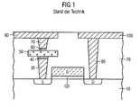
- FIG. 1shows a simplified sectional view of a phase change memory element according to the prior art, wherein in a semiconductor substrate 10, a semiconductor switching element such as a field effect transistor is formed with a source region S, a drain region D and a gate G, which lies over a gate dielectric GD.
- the source region Sis connected, for example, via a connection element 30 to a connection electrode 40, which contacts the phase change material 50 with the properties described above.
- a further terminal counter-electrode 60is provided, which is electrically connected via a further connection element 70 with a conductor track 80 in connection.
- the drain region Dcan likewise be connected to a conductor track 100 via a connection element 90.
- Reference numeral 20denotes an insulating intermediate dielectric.
- this phase change portion of the phase change material 50may have a corresponding crystallization heating or melt heating, thereby causing a phase change.
- the amorphization of the phase change materialrequires only a short time (short current pulse) but a high temperature (high current amount), while for the crystallization for a longer period of time, a lower current must be present.
- the readout of the set phase statecan be performed by applying a sufficiently low read voltage, which does not cause critical heating. Since the measured current is proportional to the conductivity or the resistance of the phase change material, the thus set phase states can be reliably detected. In addition, since the phase change material can be electrically switched almost any number of times, non-volatile memory elements can be easily generated.
- Phase change memory elementsusually realized with a selection element such as the field effect transistor shown.
- this selection elementcan also be an unillustrated bipolar transistor, a diode or another switching element in the same way.
- connection electrodeknown in which a lithographically structured pad for a phase change material is reduced by spacers such that again a very small contact surface and in particular a sublithographic contact surface of the connection electrode to the phase change material can be realized.
- connection electrode and phase change materialare not possible.
- the inventionis therefore based on the object to provide a connection electrode for phase change materials, an associated phase change memory element and an associated manufacturing method, wherein an effective contact surface and thus a spatial boundary of the current path can be adjusted with high accuracy.
- connection electrodeby the features of patent claim 1
- phase change memory elementby the features of patent claim 7
- manufacturing methodby the measures of patent claim 10.
- an electrode material of the connection electrodehas a multiplicity of insulation regions, which are formed at least on the connection surface to the phase change material.
- the electrode materialis structured lithographically, while the isolation regions are formed sublithographically.
- the insulation regionspreferably have a grain-shaped surface cross-section, wherein they consist of SiO 2 , while the electrode material has TiN.
- the terminal electrodeis preferably formed in a contact hole of a dielectric, wherein the phase change material is formed either on the surface of the dielectric outside the contact hole or only on the surface of the terminal electrode within the contact hole.
- a plurality of masking elementsare preferably formed on the surface of an auxiliary dielectric, wherein, in a subsequent step, areas of the auxiliary dielectric uncovered by the masking elements are anisotropically etched back to form a plurality of isolation regions and the resulting thereby exposed areas are filled with an electrode material for forming a terminal electrode.
- the masking elementsare formed sublithographically, wherein in particular so-called LPCVD processes for the production of semiconductor nanocrystals or HSG processes for the production of HSG grains (Hemispherical Silicon Grains) are used.
- LPCVD processesfor the production of semiconductor nanocrystals
- HSG processesfor the production of HSG grains (Hemispherical Silicon Grains) are used.
- TiN conformally as an electrode materialis deposited over the whole area by means of an ALD process and removed from a common surface of the dielectric and the insulation regions.
- the terminal electrodecan also be etched back to a predetermined depth in the contact hole and the phase change material can be formed only in this recess, resulting in a self-aligning process with maximum integration density.
- FIGS. 2A to 2Gshow simplified sectional views and a plan view for illustrating a method for producing a connection electrode for phase change materials and in particular for a phase change memory element, as for example in a phase change memory cell according to FIG. 1 can be used.
- a dielectric 2is formed on a carrier layer 1, wherein the carrier layer 1 preferably has a monocrystalline Si semiconductor substrate and the dielectric 2 has a multi-layer structure.
- the first insulating layer 2Afor example, an SiO 2 layer is deposited or thermally formed on the surface of the carrier layer 1 and the Si semiconductor substrate, respectively, and then over the entire surface of the first insulating layer 2A, a second insulating layer 2B consisting of Si 3 N 4 , for example deposited.
- the advantage of this double layeris that the second insulation layer 2B can be used as etch stop layer in a later process step.
- the carrier layer 1may also represent a metallization level or another preferably electrically conductive layer.
- a contact hole in the dielectric 2 or the first and second insulating layer 2A and 2Bis formed by means of conventional lithographic methods.
- the contact holehas an extension F, wherein F defines a minimum lithographically realizable structure width.
- the contact holemay, for example, have a rectangular, square, circular or oval shape. Usually, standard etching methods are used to form this contact hole, and detailed description will be omitted below.
- a connection element 3is now formed within this contact hole or the opening in the dielectric 2.
- a thin liner layeris deposited on the surface of the contact hole or the opening, ie on the side surfaces of the insulating layers 2A and 2B and the bottom region, and thermally cured.
- a Ti / TiN liner double layerhaving a layer thickness of 10nm / 10nm with the same layer thickness, ie conformal, is deposited and annealed at a predetermined temperature, thereby providing a reliable barrier layer for preventing outdiffusion of impurities into the semiconductor material or support layer 1 receives.
- the opening or the contact holeis filled with an electrically conductive filling layer 3B, wherein tungsten is preferably deposited over the entire surface and etched back into the opening or into the contact hole up to a predetermined depth (eg 10 nm).
- a predetermined deptheg 10 nm.
- RIEreactive ion etching
- the liner layer 3Acan be removed on the side walls of the contact hole, whereby the in FIG. 2A shown recess R in the contact hole or the opening receives.
- an isotropic and in particular a wet-chemical etching methodis used for the removal of the liner layer 3A.
- dry-chemical or directional etching processescan also be carried out.
- the recess Rcan also have a different dimension from the contact hole, wherein it preferably has a minimum realized by lithographic process structure width F to realize the required high current densities.
- an auxiliary dielectric HIis filled in the recess R.
- SiO 2is preferably deposited over the whole area by means of a CVD method (chemical vapor deposition) and then planarized to the surface of the dielectric 2 or of the second insulation layer 2B.
- CVD methodchemical vapor deposition
- an SiO 2 layer at least 10 nm thickis deposited and planarized.
- a plurality of mutually spaced masking elements Kare formed at least on the surface of the auxiliary dielectric HI.
- HSG methodHemispherical Silicon Grain
- silicon grains having a size of 5 to 15 nmare formed over the entire surface of the surface of the dielectric 2 and of the auxiliary dielectric HI.
- nanocrystals or so-called nanodotscan be produced as masking elements K, which have a feature size of 1 nm to 10 nm.
- an areal densitycan also be set or varied very well, which is important for the exact setting of an ultimately effective terminal electrode area.
- the size of the nanodots or masking elements Kis at least an order of magnitude smaller than a pattern width of the opening or the contact hole, i. the granular masking elements K have a structure width of less than 1/10 F.
- FIG. 2DAn anisotropic etching back of the region of the auxiliary dielectric HI not covered by the masking elements K up to the connection element 3 of the filling layer 3B and of the liner layer 3A can now take place. In this way, a plurality of separate isolation regions I are formed so to speak "island-shaped". Due to the Using the Si 3 N 4 insulating layer 2B, it is possible to carry out a selective etching back of the auxiliary dielectric HI using standard etching methods, which preferably consists of SiO 2 , selectively to the material of the masking elements K, ie to the silicon and to the material of the second insulating layer 2B. In principle, an undirected or only partially directed etching can be carried out, whereby the shape of the isolation regions can be influenced.
- standard etching methodswhich preferably consists of SiO 2
- the masking elements K(nanodots or HSG grains) located on the surface can be selectively removed from the auxiliary dielectric HI, the connection element 3 and the second insulation layer 2B or the dielectric 2.
- CMP processeschemical mechanical polishing
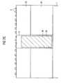
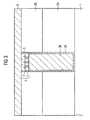
- TiNcan be conformally deposited as electrode material E and in particular over the whole area by means of an ALD method (Atomic Layer Deposition) and finally removed from the common surface of the dielectric 2 and the insulation regions I. This removal is preferably done by means of a planarization process such as a CMP process. Again, only a selectivity to the second insulating layer 2B and the material of the isolation regions I is required.
- FIG. 2Fshows a simplified plan view of the terminal electrode 4, as after the manufacturing step according to Figure 2E is present. Consequently, the connection electrode 4 has an electrode material E whose basic shape is preferably determined lithographically by the contact hole and in which a plurality of insulation regions I at least at the connection surface are formed or stored to a phase change material.
- the preferably sublithographically formed isolation regions Ithus represent a multiplicity of preferably separate islands in a "lake" of the electrode material E.
- the isolation regions Ia characteristic for this manufacturing grain-like structure on the connection surface.
- the isolation regions in cross section to the connection surface on a cylindrical structurewhich results essentially from the directed etching process.
- the insulating regions Iextend from the terminal surface 01 to an opposite major surface 02 and thus are formed "island-shaped", they may also be formed only on the terminal surface O1 and thus "float" on the electrode material E.
- Such an implementationmay, for example, result from the use of an isotropic or partially isotropic etching process, in which only insulating material remains immediately below the masking grains K and is otherwise removed.
- all or only individual isolation areas Ican also touch, as a result of which a "net-shaped" structure of the isolation areas I is created.
- a phase change material 5is formed at least on the surface of the terminal electrode 4.
- Ge x Sb y Te zis preferably deposited over the entire surface, for example by means of a PVD or CVD method, but ALD (atomic layer deposition) methods can also be used.
- a connection counterelectrode 6is formed on the main surface of the phase change material 5 opposite the connection electrode 4. Preferably, this is TiN in turn deposited over the whole area by means of a PVD, CVD or ALD method.
- the variation of the terminal electrode cross-sectional areacan be adjusted very precisely by varying the size and density of the nanodots, in particular when using LPCVD-Si nanocrystal methods. Due to the statistical distribution of the nanodots results in a very uniform distribution of the current flow over the contact surface of the terminal electrode, which is why you get a very high scalability of the process regardless of a lithography and the nanodots used.
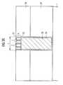
- FIG. 3shows a simplified sectional view of a phase change memory element according to a second embodiment, wherein like reference numerals the same or corresponding layers and elements as in the FIGS. 2A to 2G denote, which is why a repeated description is omitted below.
- an upper portion of the terminal electrode 4removes or the SiO 2 insulation areas I and the TiN electrode material E to a predetermined depth, which is about half the height of the original terminal electrode corresponds etched back into the contact hole.
- a phase change material 5 and in particular Ge x Sb y Te zdeposited over the entire surface and planarized up to the surface of the dielectric 2 and the second insulating layer 2B.
- a terminal counter electrode 6preferably of TiN over the entire surface deposited.
- the thickness of the phase change material 5 according to FIG. 3should typically be ⁇ 10 nm, wherein the terminal electrode 4 also has a thickness of about 10 nm.
- a phase change memory cellcan be used with the usual methods, for example according to FIG. 1 to get finished.
- the other materialsare not limited to the materials described above but may include alternative materials.
- the dielectric 2does not have to have a multilayer structure.
- the inventionis not limited to a Si semiconductor substrate as a carrier layer 1, but may be formed in the same way on other carrier layers and in particular in overlying wiring layers.
Landscapes
- Engineering & Computer Science (AREA)
- Manufacturing & Machinery (AREA)
- Semiconductor Memories (AREA)
Description
Translated fromGermanDie vorliegende Erfindung bezieht sich auf eine Anschlusselektrode für Phasen-Wechsel-Materialien, ein zugehöriges Phasen-Wechsel-Speicherelement sowie ein zugehöriges Herstellungsverfahren und insbesondere auf Anschlusselektroden, welche bei derartigen Speicherschaltungen besonders hohe Integrationsdichten ermöglichen.The present invention relates to a connection electrode for phase change materials, an associated phase change memory element and an associated manufacturing method and in particular to terminal electrodes, which allow for such memory circuits particularly high integration densities.
Sogenannte Phasen-Wechsel-Speicherelemente (phase change memory elements) verwenden Materialien, die hinsichtlich ihrer elektrischen Eigenschaften eine reversible Umschaltbarkeit von einer Phase in eine andere Phase aufweisen. Beispielsweise wechseln derartige Materialien zwischen einer amorph geordneten Phase und einer kristallin oder polykristallin geordneten Phase. Insbesondere ein Widerstand bzw. ein Leitwert eines derartigen Materials ist in diesen zwei unterschiedlichen Phasenzuständen sehr verschieden.So-called phase change memory elements use materials which, in terms of their electrical properties, have a reversible switchability from one phase to another phase. For example, such materials alternate between an amorphous ordered phase and a crystalline or polycrystalline ordered phase. In particular, a resistance or conductance of such a material is very different in these two different phase states.
In Phasen-Wechsel-Speicherelementen werden daher üblicherweise derartige Phasen-Wechsel-Materialien verwendet, die beispielsweise Legierungen von Elementen in der Gruppe VI des Periodensystems darstellen und als sogenannte Kalkogenide (chalcogenides) oder kalkogenische Materialien bezeichnet werden. Unter derartigen Phasen-Wechsel-Materialien werden demzufolge nachfolgend Materialien verstanden, die zwischen zwei unterschiedlichen Phasenzuständen mit unterschiedlichen elektrischen Eigenschaften (Widerständen) umgeschaltet werden können.In phase change memory elements therefore usually such phase change materials are used, which represent, for example, alloys of elements in the group VI of the periodic table and are referred to as so-called Kalkogenide (chalcogenides) or kalkogenische materials. Accordingly, such phase-change materials are understood below as materials that can be switched between two different phase states with different electrical properties (resistances).
Die derzeit am weitesten verbreiteten Kalkogenide bzw. Phasen-Wechsel-Materialien bestehen aus einer Legierung von Ge, Sb und Te (GexSbyTez). Ge2Sb2Te5 wird bereits in einer Vielzahl von Phasen-Wechsel-Speicherelementen verwendet und ist darüber hinaus als Material für wiederbeschreibbare optische Speichermedien (z.B. CDs, DVDs usw.) bekannt.The currently most widespread limeogens or phase change materials are made of an alloy of Ge, Sb and Te (Gex Sby Tez ). Ge2 Sb2 Te5 is already used in a variety of phase change memory elements and is also known as a material for rewritable optical storage media (eg CDs, DVDs, etc.).
Die Änderungen des Widerstandes von Phasen-Wechsel-Materialien werden genutzt, um beispielsweise nicht-flüchtige Speicherelemente (NVM, Non Volatile Memory) zu schaffen und Informationen zu speichern. In der amorphen Phase weisen demzufolge derartige Materialien einen höheren Widerstand auf als in der kristallinen oder polykristallinen Phase. Demzufolge kann ein Phasen-Wechsel-Material als programmierbarer Widerstand verwendet werden, dessen Widerstandsbetrag in Abhängigkeit von seinem Phasenzustand reversibel verändert werden kann.The changes in the resistance of phase change materials are used, for example, to create nonvolatile memory (NVM) devices and to store information. Accordingly, in the amorphous phase, such materials have a higher resistance than in the crystalline or polycrystalline phase. Accordingly, a phase change material can be used as a programmable resistor whose resistance amount can be changed reversibly depending on its phase state.
Eine Übersicht derartiger Phasen-Wechsel-Materialien ist beispielsweise aus der Literaturstelle
Ein Wechsel der Phase in derartigen Materialien kann durch eine lokale Erhöhung einer Temperatur verursacht werden. Unter 150 Grad Celsius sind üblicherweise beide Phasenzustände stabil. Über 300 Grad Celsius erfolgt eine schnelle Kernbildung von Kristallen, weshalb man eine Änderung des Phasenzustandes in einen kristallinen oder polykristallinen Zustand erhält, sofern eine derartige Temperatur ausreichend lange vorliegt. Um den Phasenzustand wiederum in den amorphen Zustand zu bringen, wird die Temperatur über den Schmelzpunkt von ca. 600 Grad Celsius gebracht und sehr schnell abgekühlt. Beide kritischen Temperaturen, sowohl für die Kristallisierung als auch für das Schmelzen, können unter Verwendung eines elektrischen Stromes erzeugt werden, der durch eine elektrisch leitende Anschlusselektrode mit einem vorbestimmten Widerstand fließt und in Kontakt oder in der Nähe des Phasen-Wechsel-Materials ist. Die Erwärmung erfolgt hierbei durch sogenannte Joule'sche Erwärmung.Phase change in such materials can be caused by a local increase in temperature. Below 150 degrees Celsius, both phase states are usually stable. Above 300 degrees Celsius, rapid nucleation of crystals takes place, which is why a change in the phase state to a crystalline or polycrystalline state is obtained if such a temperature is sufficiently long. To bring the phase state again in the amorphous state, the temperature is brought above the melting point of about 600 degrees Celsius and cooled very quickly. Both critical temperatures, both for crystallization and for melting, can be generated using an electrical current that flows through an electrically conductive terminal electrode having a predetermined resistance and in contact or in the vicinity of the phase change material is. The heating takes place here by so-called Joule'sche warming.
Das Bezugszeichen 20 bezeichnet ein isolierendes Zwischendielektrikum. Der Abschnitt des Phasen-Wechsel-Materials 50, der mit den Anschlusselektroden 40 und 60 in unmittelbarem Kontakt steht, definiert den effektiven Phasen-Wechsel-Bereich des kalkogeniden Materials.
Wird nunmehr ein elektrischer Strom mit einem ausreichend hohen Betrag durch die Anschlusselektrode 40 geschickt, so kann dieser Phasen-Wechsel-Abschnitt des Phasen-Wechsel-Materials 50 eine entsprechende Kristallisierungs-Erwärmung oder Schmelz-Erwärmung aufweisen, wodurch ein Phasenwechsel verursacht wird. Hierbei benötigt die Amorphisierung des Phasen-Wechsel-Materials lediglich eine kurze Zeit (kurzer Stromimpuls) jedoch eine hohe Temperatur (hoher Strombetrag), während für die Kristallisierung für eine längere Zeitdauer ein geringerer Strom anliegen muss.Now, when an electric current with a sufficiently high amount is sent through the
Das Auslesen des eingestellten Phasenzustandes kann durch Anlegen einer ausreichend geringen Lese-Spannung durchgeführt werden, welche keine kritische Erwärmung verursacht. Da der gemessene Strom proportional zur Leitfähigkeit bzw. zum Widerstand des Phasen-Wechsel-Materials ist, können die derart eingestellten Phasenzustände zuverlässig erfasst werden. Da darüber hinaus das Phasen-Wechsel-Material nahezu beliebig oft elektrisch umgeschaltet werden kann, können sehr einfach nicht-flüchtige Speicherelemente erzeugt werden.The readout of the set phase state can be performed by applying a sufficiently low read voltage, which does not cause critical heating. Since the measured current is proportional to the conductivity or the resistance of the phase change material, the thus set phase states can be reliably detected. In addition, since the phase change material can be electrically switched almost any number of times, non-volatile memory elements can be easily generated.
Zur Vermeidung von Störungen zwischen benachbarten Speicherelementen werden gemäß
Nachteilig sind jedoch bei derartigen Speicherelementen die sehr hohen Programmierströme, welche für die Änderung des Phasenzustandes erforderlich sind. Insbesondere in Halbleiterschaltungen mit sehr hohen Integrationsdichten sind derartige Ströme jedoch stark begrenzt, wobei z.B. bei Gatelängen von ca. 100 nm und einem verwendeten Gatedielektrikum, welches einer Spannung von 3 V widersteht, maximale Ströme von 100 bis 200 µA zur Verfügung stehen. Dadurch ergeben sich Kontaktflächen zum Phasen-Wechsel-Material von maximal 20 nm x 20 nm, welche weit unterhalb von lithographisch realisierbaren Strukturen liegen.The disadvantage, however, in such memory elements, the very high programming currents, which are required for the change of the phase state. However, especially in semiconductor circuits with very high integration densities, such currents are severely limited, e.g. With gate lengths of about 100 nm and a gate dielectric used, which withstands a voltage of 3 V, maximum currents of 100 to 200 μA are available. This results in contact surfaces for the phase change material of a maximum of 20 nm x 20 nm, which are far below lithographically realizable structures.
Zur Erzielung derartiger hoher Stromdichten bzw. kleiner Kontaktflächen ist aus der
Ferner ist aus der
Eine präzise Einstellung der tatsächlich wirkenden Kontaktfläche zwischen Anschlusselektrode und Phasen-Wechsel-Material ist jedoch dadurch nicht möglich.However, a precise adjustment of the actual effective contact surface between the connection electrode and phase change material is not possible.
Der Erfindung liegt daher die Aufgabe zu Grunde eine Anschlusselektrode für Phasen-Wechsel-Materialien, ein zugehöriges Phasen-Wechsel-Speicherelement sowie ein zugehöriges Herstellungsverfahren zu schaffen, wobei eine effektive Kontaktfläche und somit eine räumliche Begrenzung des Strompfads hochgenau eingestellt werden kann.The invention is therefore based on the object to provide a connection electrode for phase change materials, an associated phase change memory element and an associated manufacturing method, wherein an effective contact surface and thus a spatial boundary of the current path can be adjusted with high accuracy.
Erfindungsgemäß wird diese Aufgabe hinsichtlich der Anschlusselektrode durch die Merkmale des Patentanspruchs 1, hinsichtlich des Phasen-Wechsel-Speicherelements durch die Merkmale des Patentanspruchs 7 und hinsichtlich des Herstellungsverfahrens durch die Maßnahmen des Patentanspruchs 10 gelöst.According to the invention, this object is achieved with regard to the connection electrode by the features of patent claim 1, with regard to the phase change memory element by the features of patent claim 7 and with regard to the manufacturing method by the measures of
Erfindungemäß weist demzufolge ein Elektrodenmaterial der Anschlusselektrode eine Vielzahl von Isolationsgebieten auf, die zumindest an der Anschlussoberfläche zum Phasen-Wechsel-Material ausgebildet sind.According to the invention, accordingly, an electrode material of the connection electrode has a multiplicity of insulation regions, which are formed at least on the connection surface to the phase change material.
Vorzugsweise ist hierbei das Elektrodenmaterial lithographisch strukturiert, während die Isolationsgebiete sublithographisch ausgebildet werden.Preferably, in this case, the electrode material is structured lithographically, while the isolation regions are formed sublithographically.
Die Isolationsgebiete weisen hierbei vorzugsweise einen kornförmigen Oberflächenquerschnitt auf, wobei sie aus SiO2 bestehen, während das Elektrodenmaterial TiN aufweist.In this case, the insulation regions preferably have a grain-shaped surface cross-section, wherein they consist of SiO2 , while the electrode material has TiN.
Hinsichtlich des Phasen-Wechsel-Speicherelements wird die Anschlusselektrode vorzugsweise in einem Kontaktloch eines Dielektrikums ausgebildet, wobei das Phasen-Wechsel-Material entweder an der Oberfläche des Dielektrikums außerhalb des Kontaktlochs oder nur an der Oberfläche der Anschlusselektrode innerhalb des Kontaktlochs ausgebildet ist.With regard to the phase change memory element, the terminal electrode is preferably formed in a contact hole of a dielectric, wherein the phase change material is formed either on the surface of the dielectric outside the contact hole or only on the surface of the terminal electrode within the contact hole.
Hinsichtlich des Verfahrens zur Herstellung eines Phasen-Wechsel-Speicherelements werden vorzugsweise eine Vielzahl von Maskierungselementen an der Oberfläche eines Hilfsdielektrikums ausgebildet, wobei in einem nachfolgenden Schritt von den Maskierungselementen nicht bedeckte Bereiche des Hilfsdielektrikums zum Ausbilden einer Vielzahl von Isolationsgebieten anisotrop rückgeätzt werden und die dadurch entstehenden freiliegenden Bereiche mit einem Elektrodenmaterial zum Ausbilden einer Anschlusselektrode aufgefüllt werden.With regard to the method for producing a phase change memory element, a plurality of masking elements are preferably formed on the surface of an auxiliary dielectric, wherein, in a subsequent step, areas of the auxiliary dielectric uncovered by the masking elements are anisotropically etched back to form a plurality of isolation regions and the resulting thereby exposed areas are filled with an electrode material for forming a terminal electrode.
Vorzugsweise werden die Maskierungselemente sublithographisch ausgebildet, wobei insbesondere sogenannte LPCVD-Verfahren zur Herstellung von Halbleiter-Nanokristallen oder HSG-Verfahren zur Herstellung von HSG-Körnern (Hemispherical Silicon Grains) verwendet werden.Preferably, the masking elements are formed sublithographically, wherein in particular so-called LPCVD processes for the production of semiconductor nanocrystals or HSG processes for the production of HSG grains (Hemispherical Silicon Grains) are used.
Als Elektrodenmaterial wird insbesondere TiN konformal mittels eines ALD-Verfahrens ganzflächig abgeschieden und von einer gemeinsamen Oberfläche des Dielektrikums und der Isolationsgebiete entfernt.In particular, TiN conformally as an electrode material is deposited over the whole area by means of an ALD process and removed from a common surface of the dielectric and the insulation regions.
Alternativ kann die Anschlusselektrode auch bis zu einer vorbestimmten Tiefe im Kontaktloch zurückgeätzt werden und das Phasen-Wechsel-Material nur in dieser Vertiefung ausgebildet werden, wodurch sich ein selbstjustierendes Verfahren mit maximaler Integrationsdichte ergibt.Alternatively, the terminal electrode can also be etched back to a predetermined depth in the contact hole and the phase change material can be formed only in this recess, resulting in a self-aligning process with maximum integration density.
In den weiteren Unteransprüchen sind weitere vorteilhafte Ausgestaltungen der Erfindung gekennzeichnet.In the further subclaims further advantageous embodiments of the invention are characterized.
Die Erfindung wird nachstehend anhand von Ausführungsbeispielen unter Bezugnahme auf die Zeichnung näher beschrieben.The invention will be described below with reference to embodiments with reference to the drawings.
Es zeigen:
Figur 1 eine vereinfachte Schnittansicht eines Phasen-Wechsel-Speicherelements gemäß dem Stand der Technik;Figuren 2A bis 2GFigur 3 eine vereinfachte Schnittansicht zur Veranschaulichung eines Phasen-Wechsel-Speicherelements mit erfindungsgemäßer Anschlusselektrode gemäß einem zweiten Ausführungsbeispiel.
FIG. 1 a simplified sectional view of a phase change memory element according to the prior art;FIGS. 2A to 2G simplified sectional views and a plan view for illustrating essential manufacturing steps in the realization of a phase change memory element with inventive connecting electrode according to a first embodiment; andFIG. 3 a simplified sectional view illustrating a phase change memory element with inventive connecting electrode according to a second embodiment.
Gemäß
Grundsätzlich sind auch andere Isolationsschichten und insbesondere alternative zwischendielektrische Schichten als Dielektrikum 2 zu verwenden. In gleicher Weise kann die Trägerschicht 1 auch eine Metallisierungsebene oder eine sonstige vorzugsweise elektrisch leitende Schicht darstellen.In principle, other insulating layers and in particular alternative interdielectric layers are to be used as the
Zur Realisierung einer elektrischen Verbindung zu einem im Halbleitermaterial ausgebildeten Auswahlelement wie beispielsweise dem Sourcegebiet S gemäß
Gemäß
Nach dieser Liner-Abscheidung erfolgt ein Auffüllen der Öffnung bzw. des Kontaktlochs mit einer elektrisch leitenden Füllschicht 3B, wobei vorzugsweise Wolfram ganzflächig abgeschieden und bis zu einer vorbestimmten Tiefe (z.B. 10nm) in die Öffnung bzw. in das Kontaktloch hinein zurückgeätzt wird. Eine derartige Rückätzung kann beispielsweise mittels eines Trockenätzverfahrens und insbesondere mittels reaktiven Ionenätzens (RIE, Reactive Ion Etch) durchgeführt werden. Ferner kann in diesem oberen Abschnitt auch die Linerschicht 3A an den Seitenwänden des Kontaktlochs entfernt werden, wodurch man die in
Gemäß
Gemäß
Mittels dieses Verfahrens können Nanokristalle bzw. sogenannte Nanodots als Maskierungselemente K erzeugt werden, die eine Strukturgröße von 1 nm bis 10 nm aufweisen. Hierbei lässt sich neben der jeweiligen Größe dieser Nanodots bzw. Maskierungselemente K auch eine Flächendichte sehr gut einstellen bzw. variieren, was zur exakten Einstellung einer letztlich effektiven Anschlusselektrodenfläche von Bedeutung ist. Vorzugsweise ist die Größe der Nanodots bzw. Maskierungselementen K um mindestens eine Größenordnung kleiner als eine Strukturbreite der Öffnung bzw. des Kontaktlochs, d.h. die kornförmigen Maskierungselemente K weisen eine Strukturbreite kleiner 1/10 F auf.By means of this method, nanocrystals or so-called nanodots can be produced as masking elements K, which have a feature size of 1 nm to 10 nm. In addition to the respective size of these nanodots or masking elements K, an areal density can also be set or varied very well, which is important for the exact setting of an ultimately effective terminal electrode area. Preferably, the size of the nanodots or masking elements K is at least an order of magnitude smaller than a pattern width of the opening or the contact hole, i. the granular masking elements K have a structure width of less than 1/10 F.
Gemäß
Gemäß
Ferner wird gemäß
Obwohl sich gemäß
Gemäß
Die Vervollständigung einer derartigen nicht flüchtigen Speicherzelle erfolgt dann gemäß dem Stand der Technik, wie z.B. in
Auf diese Weise erhält man eine Anschlusselektrode 4 sowie ein zugehöriges Phasen-Wechsel-Speicherelement sowie ein zugehöriges Herstellungsverfahren, bei dem der benötigte Schaltstrom sich durch die räumliche Begrenzung des Strompfades sehr genau verringern und einstellen lässt, weshalb auch bei hohen Integrationsdichten die erforderlichen jouleschen Erwärmungen mit sehr geringen Stromstärken realisierbar sind.In this way, one obtains a
Die Variation der Anschlusselektroden-Querschnittsfläche lässt sich insbesondere bei Verwendung von LPCVD-Si-Nanokristall-Verfahren sehr genau durch Variation der Größe und Dichte der Nanodots einstellen. Auf Grund der statistischen Verteilung der Nanodots ergibt sich eine sehr gleichmäßige Verteilung des Stromflusses über die Kontaktfläche der Anschlusselektrode, weshalb man eine sehr hohe Skalierbarkeit des Prozesses unabhängig von einer verwendeten Lithographie und den verwendeten Nanodotgrößen erhält.The variation of the terminal electrode cross-sectional area can be adjusted very precisely by varying the size and density of the nanodots, in particular when using LPCVD-Si nanocrystal methods. Due to the statistical distribution of the nanodots results in a very uniform distribution of the current flow over the contact surface of the terminal electrode, which is why you get a very high scalability of the process regardless of a lithography and the nanodots used.
Gemäß diesem zweiten Ausführungsbeispiel wird nach einem Schritt gemäß
Abschließend wird wie beim ersten Ausführungsbeispiel gemäß
Die Erfindung wurde vorstehend anhand von GexSbyTez als Phasen-Wechsel-Material beschrieben. Sie ist jedoch nicht darauf beschränkt und umfasst in gleicher Weise auch alternative Phasen-Wechsel-Materialien.The invention has been described above with reference to Gex Sby Tez as a phase change material. However, it is not limited thereto and equally includes alternative phase change materials.
In gleicher Weise sind die weiteren Materialien nicht auf die vorstehend beschriebenen Materialien beschränkt sondern können alternative Materialien umfassen. Insbesondere muss das Dielektrikum 2 keinen Mehrschichtaufbau aufweisen.Likewise, the other materials are not limited to the materials described above but may include alternative materials. In particular, the
Ferner ist die Erfindung nicht auf ein Si-Halbleitersubstrat als Trägerschicht 1 beschränkt, sondern kann in gleicher Weise auch auf sonstigen Trägerschichten und insbesondere in darüber liegenden Verdrahtungsschichten ausgebildet sein.Furthermore, the invention is not limited to a Si semiconductor substrate as a carrier layer 1, but may be formed in the same way on other carrier layers and in particular in overlying wiring layers.
Claims (22)
- Connection electrode for phase change material, having an electrically conductive electrode material (E), which has at least one connection surface (O1) for the phase change material,characterized in that a multiplicity of insulation regions (I) are formed within the electrode material (E) and at least at its connection surface (O1), in order to reduce the overall size of a contact surface.
- Connection electrode according to Patent Claim 1,characterized in that the insulation regions (I) are sublithographically patterned, and the electrode material (E) is formed cohesively between the insulation regions (I).
- Connection electrode according to either of Patent Claims 1 and 2,characterized in that the insulation regions (I) extend from the connection surface (O1) to an opposite main surface (02).
- Connection electrode according to one of Patent Claims 1 to 3,characterized in that the insulation regions (I) have a grain-like structure at the connection surface (O1).
- Connection electrode according to either of Patent Claims 3 and 4,characterized in that the insulation regions (I) have a cylindrical structure in cross section with respect to the connection surface (O1).
- Connection electrode according to one of Patent Claims 1 to 5,characterized in that the insulation regions (I) include SiO2 and the electrode material (E) includes TiN.
- Phase change memory element, having
a carrier layer (1);
a connection element (3), which is electrically connected to the carrier layer (1);
a connection electrode (4) having a connection surface (O1) and an opposite main surface (02), which is electrically connected to the connection element (3);
a phase change material (5), which is formed at the connection surface (O1); and
a connection counterelectrode (6), which is formed on the phase change material (5) on the opposite side from the connection electrode (4),
characterized in that the connection electrode (4) and/or the connection counterelectrode (6) is formed as described in one of Patent Claims 1 to 6. - Phase change memory element according to Patent Claim 7,characterized in that the connection element (3) and the connection electrode (4) are formed in a contact hole of a dielectric (2), and the phase change material (5) is formed at the common surface of the dielectric (2) and the connection electrode (4).
- Phase change memory element according to Patent Claim 7,characterized in that the connection element (3), the connection electrode (4) and the phase change material (5) are formed in a contact hole of a dielectric (2), and
the connection counterelectrode (6) is formed at the common surface of the dielectric (2) and the phase change material (5). - Process for producing a phase change memory element, comprising the steps of:a) forming a dielectric (2) on a carrier layer (1);b) forming an opening in the dielectric (2) as far as the carrier layer (1);c) forming a connection element (3) in the opening;d) forming a recess (R) in the region of the connection element (3);e) filling the recess (R) with an auxiliary dielectric (HI);f) forming a multiplicity of masking elements (K) at least at the surface of the auxiliary dielectric (HI);g) anisotropically etching back those regions of the auxiliary dielectric (HI) which are not covered by the masking elements (K) as far as the connection element (3), to form a multiplicity of insulation regions (I);h) filling the regions which lie between the insulation regions (I) with an electrode material (E) to form a connection electrode (4);i) forming a phase change material (5) at least at the surface of the connection electrode (4); andj) forming a connection counterelectrode (6) at the opposite main surface of the phase change material (5).
- Process according to Patent Claim 10,characterized in that in step a) a first insulation layer (2A), in particular SiO2, is deposited on the carrier layer (1), in particular an Si substrate, and a second insulation layer (2B), in particular Si3N4, is deposited on the first insulation layer (2A).
- Process according to Patent Claim 10 or 11,characterized in that in step b) a contact hole is formed as the opening by means of a lithographic process.
- Process according to one of Patent Claims 10 to 12,characterized in that in step c) an electrically conductive liner (3A), in particular Ti/TiN, is deposited at the surface of the opening and annealed, and an electrically conductive filling layer (3B), in particular W, is deposited thereon.
- Process according to one of Patent Claims 10 to 13,characterized in that in step d) the connection element (3) is etched back in the opening.
- Process according to one of Patent Claims 10 to 14,characterized in that in step e) SiO2 is deposited over the entire surface and planarized.
- Process according to one of Patent Claims 10 to 15,characterized in that in step f) the masking elements (K) are formed sublithographically.
- Process according to Patent Claim 16,characterized in that nanocrystals, in particular Si nanocrystals, are deposited over the entire surface by means of an LPCVD process.
- Process according to Patent Claim 16,characterized in that HSG grains are deposited over the entire surface.
- Process according to one of Patent Claims 10 to 18,characterized in that in step h) the electrode material (E), in particular TiN, is deposited conformally, in particular by means of an ALD process, over the entire surface and is removed from the common surface of the dielectric (2) and the insulation regions (I).
- Process according to one of Patent Claims 10 to 19,characterized in that in step i) the phase change material (5), in particular GexSbyTez, is deposited over the entire surface by means of a PVD or CVD process.
- Process according to one of Patent Claims 10 to 19,characterized in that in step i) the connection electrode (4) is etched back to a predetermined depth, the phase change material (5), in particular GexSbyTez, is deposited over the entire surface by means of a PVD or CVD process, and
a planarization is carried out. - Process according to one of Patent Claims 10 to 21,characterized in that in step j) the connection counterelectrode (6), in particular TiN, is deposited over the entire surface.
Applications Claiming Priority (1)
| Application Number | Priority Date | Filing Date | Title |
|---|---|---|---|
| DE102005014645ADE102005014645B4 (en) | 2005-03-31 | 2005-03-31 | Connection electrode for phase change material, associated phase change memory element and associated manufacturing method |
Publications (3)
| Publication Number | Publication Date |
|---|---|
| EP1708292A2 EP1708292A2 (en) | 2006-10-04 |
| EP1708292A3 EP1708292A3 (en) | 2007-09-19 |
| EP1708292B1true EP1708292B1 (en) | 2008-09-10 |
Family
ID=36600199
Family Applications (1)
| Application Number | Title | Priority Date | Filing Date |
|---|---|---|---|
| EP06110958ANot-in-forceEP1708292B1 (en) | 2005-03-31 | 2006-03-10 | Connection electrode for phase change material, corresponding phase change memory element and production method thereof |
Country Status (5)
| Country | Link |
|---|---|
| US (1) | US20070145346A1 (en) |
| EP (1) | EP1708292B1 (en) |
| JP (1) | JP2006287222A (en) |
| KR (1) | KR100789045B1 (en) |
| DE (2) | DE102005014645B4 (en) |
Families Citing this family (17)
| Publication number | Priority date | Publication date | Assignee | Title |
|---|---|---|---|---|
| DE102005014645B4 (en) | 2005-03-31 | 2007-07-26 | Infineon Technologies Ag | Connection electrode for phase change material, associated phase change memory element and associated manufacturing method |
| DE102006023608B4 (en)* | 2006-05-19 | 2009-09-03 | Qimonda Ag | Programmable resistive memory cell with a programmable resistive layer and method of manufacture |
| US7649242B2 (en) | 2006-05-19 | 2010-01-19 | Infineon Technologies Ag | Programmable resistive memory cell with a programmable resistance layer |
| US8188569B2 (en)* | 2006-12-15 | 2012-05-29 | Qimonda Ag | Phase change random access memory device with transistor, and method for fabricating a memory device |
| TW200849488A (en)* | 2007-06-08 | 2008-12-16 | Nanya Technology Corp | Deep trench and fabricating method thereof, trench capacitor and fabricating method thereof |
| US7906368B2 (en) | 2007-06-29 | 2011-03-15 | International Business Machines Corporation | Phase change memory with tapered heater |
| JP2009135219A (en) | 2007-11-29 | 2009-06-18 | Renesas Technology Corp | Semiconductor device and manufacturing method thereof |
| KR100956773B1 (en)* | 2007-12-26 | 2010-05-12 | 주식회사 하이닉스반도체 | Phase change memory device and manufacturing method thereof |
| KR100968448B1 (en)* | 2007-12-27 | 2010-07-07 | 주식회사 하이닉스반도체 | Phase change memory device and manufacturing method thereof |
| WO2009122582A1 (en)* | 2008-04-03 | 2009-10-08 | 株式会社 東芝 | Nonvolatile recording device and process for producing the same |
| WO2009122583A1 (en)* | 2008-04-03 | 2009-10-08 | 株式会社 東芝 | Nonvolatile recording device and process for producing the same |
| KR20100041139A (en)* | 2008-10-13 | 2010-04-22 | 삼성전자주식회사 | Methods of manufacturing a multi-level cell for storing multiple bits data in one memory cell by using parallel structure of phase change material |
| KR101035155B1 (en) | 2008-11-07 | 2011-05-17 | 주식회사 하이닉스반도체 | Phase change memory device and manufacturing method thereof |
| US8030130B2 (en)* | 2009-08-14 | 2011-10-04 | International Business Machines Corporation | Phase change memory device with plated phase change material |
| US20110057161A1 (en)* | 2009-09-10 | 2011-03-10 | Gurtej Sandhu | Thermally shielded resistive memory element for low programming current |
| US20110108792A1 (en)* | 2009-11-11 | 2011-05-12 | International Business Machines Corporation | Single Crystal Phase Change Material |
| JP2011211101A (en)* | 2010-03-30 | 2011-10-20 | Sony Corp | Memory device and method of manufacturing the same |
Family Cites Families (15)
| Publication number | Priority date | Publication date | Assignee | Title |
|---|---|---|---|---|
| DE69434745T2 (en)* | 1993-11-02 | 2006-10-05 | Matsushita Electric Industrial Co., Ltd., Kadoma | Method for producing an aggregate of micro-needles made of semiconductor material and method for producing a semiconductor component with such an aggregate |
| US6147395A (en)* | 1996-10-02 | 2000-11-14 | Micron Technology, Inc. | Method for fabricating a small area of contact between electrodes |
| CN1311553C (en)* | 2001-12-12 | 2007-04-18 | 松下电器产业株式会社 | Non-volatile memory and its manufacturing method |
| US6512241B1 (en)* | 2001-12-31 | 2003-01-28 | Intel Corporation | Phase change material memory device |
| US6670628B2 (en)* | 2002-04-04 | 2003-12-30 | Hewlett-Packard Company, L.P. | Low heat loss and small contact area composite electrode for a phase change media memory device |
| KR100437458B1 (en)* | 2002-05-07 | 2004-06-23 | 삼성전자주식회사 | Phase change memory cells and methods of fabricating the same |
| KR100448893B1 (en)* | 2002-08-23 | 2004-09-16 | 삼성전자주식회사 | Phase-changeable memory device and method for fabricating the same |
| JP2006502578A (en) | 2002-10-11 | 2006-01-19 | コーニンクレッカ フィリップス エレクトロニクス エヌ ヴィ | Electronic device with phase change material |
| DE60328960D1 (en)* | 2003-04-16 | 2009-10-08 | St Microelectronics Srl | Self-aligning process for making a phase change memory cell and phase change memory cell made thereby |
| KR100504701B1 (en)* | 2003-06-11 | 2005-08-02 | 삼성전자주식회사 | Phase change memory device and method for forming the same |
| KR20050001169A (en)* | 2003-06-27 | 2005-01-06 | 삼성전자주식회사 | Method for forming a PRAM |
| US20050018526A1 (en)* | 2003-07-21 | 2005-01-27 | Heon Lee | Phase-change memory device and manufacturing method thereof |
| KR100615586B1 (en)* | 2003-07-23 | 2006-08-25 | 삼성전자주식회사 | Phase change memory device having a local phase change region in a porous dielectric film and a method of manufacturing the same |
| DE10356285A1 (en)* | 2003-11-28 | 2005-06-30 | Infineon Technologies Ag | Integrated semiconductor memory and method for manufacturing an integrated semiconductor memory |
| DE102005014645B4 (en) | 2005-03-31 | 2007-07-26 | Infineon Technologies Ag | Connection electrode for phase change material, associated phase change memory element and associated manufacturing method |
- 2005
- 2005-03-31DEDE102005014645Apatent/DE102005014645B4/ennot_activeExpired - Fee Related
- 2006
- 2006-03-10DEDE502006001524Tpatent/DE502006001524D1/ennot_activeExpired - Fee Related
- 2006-03-10EPEP06110958Apatent/EP1708292B1/ennot_activeNot-in-force
- 2006-03-28USUS11/390,560patent/US20070145346A1/ennot_activeAbandoned
- 2006-03-29JPJP2006090900Apatent/JP2006287222A/enactivePending
- 2006-03-30KRKR1020060028796Apatent/KR100789045B1/ennot_activeExpired - Fee Related
Also Published As
| Publication number | Publication date |
|---|---|
| DE502006001524D1 (en) | 2008-10-23 |
| EP1708292A2 (en) | 2006-10-04 |
| DE102005014645A1 (en) | 2006-10-05 |
| DE102005014645B4 (en) | 2007-07-26 |
| KR100789045B1 (en) | 2007-12-26 |
| EP1708292A3 (en) | 2007-09-19 |
| US20070145346A1 (en) | 2007-06-28 |
| KR20060105555A (en) | 2006-10-11 |
| JP2006287222A (en) | 2006-10-19 |
Similar Documents
| Publication | Publication Date | Title |
|---|---|---|
| EP1708292B1 (en) | Connection electrode for phase change material, corresponding phase change memory element and production method thereof | |
| DE112018000142B4 (en) | Method for integrating a delimited phase change memory with material that switches at a threshold value | |
| DE10297191B4 (en) | Phase change material storage component and method of manufacture | |
| DE102008016522B4 (en) | Phase change memory cell with phase change memory material with limited resistance, method for producing a deratigen memory cell and integrated circuit with corresponding memory cell | |
| EP1685569B1 (en) | Phase change memory, phase change memory assembly, phase change memory cell, 2d phase change memory cell array, 3d phase change memory cell array and electronic component | |
| DE69827598T2 (en) | MEMORY ELEMENT WITH ENERGY CONTROL MECHANISM | |
| DE60224622T2 (en) | One-time programmable memory | |
| DE60032129T2 (en) | ELECTRICALLY PROGRAMMABLE STORAGE ELEMENT WITH IMPROVED CONTACTS | |
| DE102018106929A1 (en) | PCRAM structure with selection device | |
| DE102008045963B4 (en) | Multi-level memory and method for operating the same | |
| DE112011101925T5 (en) | Integration of a phase change memory process with a mask | |
| DE102006041849A1 (en) | Electrically rewritable non-volatile memory element and method of making the same | |
| DE102004052611A1 (en) | Method for producing an opening at least partially filled with a filling material, method for producing a memory cell and memory cell | |
| DE102008041810A1 (en) | Phase change memory device for multi-bit storage | |
| DE102005001902B4 (en) | Method for producing a sublithographic contact structure in a memory cell | |
| DE102021110683A1 (en) | STORAGE CELL COMPONENT WITH THIN FILM TRANSISTOR SELECTOR AND METHOD OF FORMING THE SAME | |
| DE102004011430B4 (en) | Semiconductor memory device | |
| DE102004041893B4 (en) | Process for the production of memory devices (PCRAM) with memory cells based on a phase-changeable layer | |
| DE10236439B3 (en) | Memory arrangement comprises a substrate, memory regions formed in and/or on the substrate with electrical resistances that can be adjusted by thermal treatment and structure arranged between the memory regions to remove heat | |
| DE112008001618B4 (en) | Electronic component and method for producing such | |
| DE102007054641A1 (en) | Integrated circuit, has selection transistor designed as vertical transistor, and metalliferous region partially staying in connection with earth plate and/or ground plate, where metalliferous region extends below selection transistor | |
| DE102005051973B3 (en) | Production method for vertical track structure, memory device and associated manufacturing method | |
| DE10297692B4 (en) | Devices and systems with adhesive material for programmable devices, and method of manufacture | |
| DE102004054558A1 (en) | Phase change random access memory cell manufacturing method, involves back etching portion of structured hard mask by isotropic etching and back etching upper electrode layer and switching active layer by dry etching | |
| DE102004015899B4 (en) | Manufacturing method for a PCM memory element |
Legal Events
| Date | Code | Title | Description |
|---|---|---|---|
| PUAI | Public reference made under article 153(3) epc to a published international application that has entered the european phase | Free format text:ORIGINAL CODE: 0009012 | |
| AK | Designated contracting states | Kind code of ref document:A2 Designated state(s):AT BE BG CH CY CZ DE DK EE ES FI FR GB GR HU IE IS IT LI LT LU LV MC NL PL PT RO SE SI SK TR | |
| AX | Request for extension of the european patent | Extension state:AL BA HR MK YU | |
| PUAL | Search report despatched | Free format text:ORIGINAL CODE: 0009013 | |
| AK | Designated contracting states | Kind code of ref document:A3 Designated state(s):AT BE BG CH CY CZ DE DK EE ES FI FR GB GR HU IE IS IT LI LT LU LV MC NL PL PT RO SE SI SK TR | |
| AX | Request for extension of the european patent | Extension state:AL BA HR MK YU | |
| 17P | Request for examination filed | Effective date:20071005 | |
| GRAP | Despatch of communication of intention to grant a patent | Free format text:ORIGINAL CODE: EPIDOSNIGR1 | |
| RIN1 | Information on inventor provided before grant (corrected) | Inventor name:SEIDL, HARALD | |
| RAP1 | Party data changed (applicant data changed or rights of an application transferred) | Owner name:QIMONDA AG | |
| GRAS | Grant fee paid | Free format text:ORIGINAL CODE: EPIDOSNIGR3 | |
| AKX | Designation fees paid | Designated state(s):DE FR GB | |
| GRAA | (expected) grant | Free format text:ORIGINAL CODE: 0009210 | |
| AK | Designated contracting states | Kind code of ref document:B1 Designated state(s):DE FR GB | |
| REG | Reference to a national code | Ref country code:GB Ref legal event code:FG4D Free format text:NOT ENGLISH | |
| REF | Corresponds to: | Ref document number:502006001524 Country of ref document:DE Date of ref document:20081023 Kind code of ref document:P | |
| PLBE | No opposition filed within time limit | Free format text:ORIGINAL CODE: 0009261 | |
| STAA | Information on the status of an ep patent application or granted ep patent | Free format text:STATUS: NO OPPOSITION FILED WITHIN TIME LIMIT | |
| 26N | No opposition filed | Effective date:20090611 | |
| REG | Reference to a national code | Ref country code:FR Ref legal event code:ST Effective date:20091130 | |
| PG25 | Lapsed in a contracting state [announced via postgrant information from national office to epo] | Ref country code:DE Free format text:LAPSE BECAUSE OF NON-PAYMENT OF DUE FEES Effective date:20091001 | |
| PG25 | Lapsed in a contracting state [announced via postgrant information from national office to epo] | Ref country code:FR Free format text:LAPSE BECAUSE OF NON-PAYMENT OF DUE FEES Effective date:20091123 | |
| GBPC | Gb: european patent ceased through non-payment of renewal fee | Effective date:20100310 | |
| PG25 | Lapsed in a contracting state [announced via postgrant information from national office to epo] | Ref country code:GB Free format text:LAPSE BECAUSE OF NON-PAYMENT OF DUE FEES Effective date:20100310 |