EP1696568A1 - Multi-bit digital input using a single pin - Google Patents
Multi-bit digital input using a single pinDownload PDFInfo
- Publication number
- EP1696568A1 EP1696568A1EP06005886AEP06005886AEP1696568A1EP 1696568 A1EP1696568 A1EP 1696568A1EP 06005886 AEP06005886 AEP 06005886AEP 06005886 AEP06005886 AEP 06005886AEP 1696568 A1EP1696568 A1EP 1696568A1
- Authority
- EP
- European Patent Office
- Prior art keywords
- voltage
- address
- digital
- bit digital
- input
- Prior art date
- Legal status (The legal status is an assumption and is not a legal conclusion. Google has not performed a legal analysis and makes no representation as to the accuracy of the status listed.)
- Granted
Links
- 238000000034methodMethods0.000claimsabstractdescription24
- 230000005540biological transmissionEffects0.000claimsabstract2
- 238000012795verificationMethods0.000claimsdescription6
- 238000004891communicationMethods0.000claimsdescription5
- 238000012935AveragingMethods0.000description13
- 238000010586diagramMethods0.000description7
- 230000008859changeEffects0.000description4
- 238000013461designMethods0.000description3
- 230000003068static effectEffects0.000description3
- 230000009471actionEffects0.000description2
- 230000008901benefitEffects0.000description2
- 238000004519manufacturing processMethods0.000description2
- 238000000926separation methodMethods0.000description2
- 238000004364calculation methodMethods0.000description1
- 238000006243chemical reactionMethods0.000description1
- 230000008878couplingEffects0.000description1
- 238000010168coupling processMethods0.000description1
- 238000005859coupling reactionMethods0.000description1
- 230000008569processEffects0.000description1
- 238000012545processingMethods0.000description1
- 230000004044responseEffects0.000description1
- 230000008054signal transmissionEffects0.000description1
- 238000010200validation analysisMethods0.000description1
Images


Classifications
- H—ELECTRICITY
- H03—ELECTRONIC CIRCUITRY
- H03K—PULSE TECHNIQUE
- H03K19/00—Logic circuits, i.e. having at least two inputs acting on one output; Inverting circuits
- H03K19/02—Logic circuits, i.e. having at least two inputs acting on one output; Inverting circuits using specified components
- H03K19/173—Logic circuits, i.e. having at least two inputs acting on one output; Inverting circuits using specified components using elementary logic circuits as components
- H03K19/1731—Optimisation thereof
- H03K19/1732—Optimisation thereof by limitation or reduction of the pin/gate ratio
- H—ELECTRICITY
- H04—ELECTRIC COMMUNICATION TECHNIQUE
- H04L—TRANSMISSION OF DIGITAL INFORMATION, e.g. TELEGRAPHIC COMMUNICATION
- H04L25/00—Baseband systems
- H04L25/38—Synchronous or start-stop systems, e.g. for Baudot code
- H04L25/40—Transmitting circuits; Receiving circuits
- H04L25/49—Transmitting circuits; Receiving circuits using code conversion at the transmitter; using predistortion; using insertion of idle bits for obtaining a desired frequency spectrum; using three or more amplitude levels ; Baseband coding techniques specific to data transmission systems
Definitions
- a device in an electronic systemmay require a multi-bit digital address or number as an input.
- This numbermay represent an address on a serial bus, a configuration word, a system serial number, or some other information required by the device. Often this number is static, or changes infrequently during the operation of the device. In these circumstances-i.e., where this number is static or requires changes only infrequently - - this number is typically required at device startup.
- a simple way to input such a number to the deviceis to have several external pins, each corresponding to a bit of the input word. Each pin is tied to either a high or low value to represent the binary bits of the input word. While straightforward, this technique requires N external electrical connections, where N is the number of bits in the input word. If the device is an integrated circuit in a low-pin-count package, these input bits may consume most of the pins on the device, leaving few for other functionality. Thus, utilizing N pins, where each pin accepts one binary bit, limits the usefulness of the device and is, therefore, a sub-optimal design solution.
- the numeric inputcould also be programmed into the electronic device at the time of manufacture or system assembly, or could be transferred into the device through a single pin using a serial communication protocol.
- each of these methodsrequires significant additional complexity in the system architecture or manufacturing process.
- circuits and methodsthat utilize a single pin to accept a single signal corresponding to a multi-bit digital address, number, or signal as required by the electronic device.
- a method of configuring an electronic device via a single input pin of the electronic deviceis provided.
- the methodpreferably utilizes a first multi-bit digital address that was encoded as a first voltage signal.
- the methodpreferably includes receiving the first voltage signal at the single input pin of the electronic device. After the first voltage signal is received at the single input pin, the method further includes converting the first voltage signal received at the input pin into the first multi-bit digital address, and configuring the electronic device using the first multi-bit digital address.
- FIG. 1is a schematic diagram of a circuit according to the invention
- FIG. 2Ais a schematic diagram of a circuit according to the invention including an analog-to-digital converter according to the invention
- FIG. 2Bis a schematic diagram of a circuit according to the invention including an analog-to-digital converter having an internal voltage reference according to the invention
- FIG. 3is a schematic diagram of a circuit according to the invention that verifies the input voltage
- FIG. 4is a schematic diagram of a circuit according to the invention including a digital comparator
- FIG. 5is a schematic diagram of a circuit according to the invention including an averaging circuit
- FIG. 6is another schematic diagram of a circuit according to the invention including an averaging circuit.
- Circuits and methods according to the inventionpreferably include inputting a single voltage signal, preferably via a single pin, corresponding to a multi-bit digital value.
- the digital valuepreferably includes a pre-determined number of bits.
- a device which utilizes circuits and methods according to the inventionpreferably includes a power supply connection, a ground connection, each of which are connected to the device at respective input pins, and a third input pin.
- Other I/O pinsmay also be required for the device to function according to the individual requirements of the device.
- a specific voltageis applied to the input pin.
- the voltagepreferably corresponds,.according to a pre-determined protocol, to a multi-bit digital signal.
- This voltageis then, in turn, converted by an analog-to-digital converter or other suitable circuitry into the multi-bit digital input signal required by the device.
- the signal transferred to the single input voltage at the pinsets the desired multi-bit digital input signal for the electronic device.
- each of the several bits, which are encoded within the voltage signalare programmed into the device substantially simultaneously, thereby reducing the time to program the multi-bit digital input signal.
- the desired multi-bit digital input signalmay be represented at the input to the device by a voltage which is a pre-determined, preferably fixed, fraction or ratio of the total power supply voltage, or it may be referenced to an absolute voltage standard or reference. This fraction or ratio may be converted into the required multi-bit digital input signal. Further details of the invention will be explained below with respect to FIGS. 1-5.
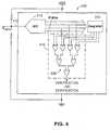
- FIG. 1shows an embodiment of a device 100 according to the invention that includes a power supply, Vcc, a ground pin and an input pin 110.
- Device 100may also include other I/O pins 120 for transmitting digital or analog signals either to or from device 100 as required by device 100.
- the input voltage at input pin 110is preferably programmed by the value of the resistors 130 and 140 because these resistors function as a voltage divider that provides a voltage that is some known portion of Vcc.
- the resistor valuesshould preferably be chosen such that the voltage at input pin 110 is a fixed percentage of the voltage between the Vcc and ground pins.
- Device 100may be utilized in a device that requires a 2-bit digital number as an input.
- "00”may preferably correspond to an input voltage between 0% and 25% of the power-to-ground voltage
- "01”may preferably correspond to an input voltage between 25% to 50%
- "10" to 50% to 75%and "11” to 75% to 100%.
- the determination of the range of percentages in which the voltage fallsmay preferably be obtained using a number or group of different comparators (not shown) in the electronic device, as is known in the art, in order to accurately determine the value (or range) of the incoming voltage.
- the value (or range)may then be transferred as a single voltage -- e.g., from the midpoint of the range -- to an analog-to-digital converter (as shown in FIGS. 2A and 2B) in order to derive the multi-bit digital address.
- resistors 130 and 140may preferably be implemented as variable resistors with the levels of variation determined by the required number of bits in the multi-bit digital input value (or binary number).
- the voltage ranges at the input pin that correspond to individual digital valuescan be evenly sized and spaced across the available voltage range.
- the voltage ranges at the input pincan have unequal sizes and spaces.
- Equal-sized/spaced rangesease calculation of error tolerances and are conceptually simpler.
- conventional 10% margin-for-error resistorsmay be used to generate 2 input bits or 4 possible numeric inputs (as described above with respect to FIG. 1) without the risk of resistor tolerance error causing a false input reading.
- 1% error resistorsmay be used to generate 5 bits or 32 possible inputs, and 0.1% resistors may be used to generate up to 8 bits or 256 inputs.
- Unequal-sized/spaced rangescan also be used to simplify the choice of external resistor values. This may be accomplished by choosing the range of the resistors so that a resistor divider is used with two fixed resistors or with one resistor value fixed and one resistor value varying in a linear manner may be used to select the desired input.
- the resistor valuemay preferably vary, or be adjustable, in known incremental values. Or, in an alternative embodiment, the resistor value may vary, or be adjustable, in a smoothed fashion.
- FIG. 2Ashows another embodiment of the invention in which device 200 may communicate over a serial digital interface bus, such as an I 2 C bus made by Phillips Electronics of the Netherlands, and notifies and/or identifies the central processing unit of a unique address to write data to, to transmit data from, or to configure device 200.
- the selected address that should be identified to receive and/or transmit the signalmay be programmed as a resistor-divided voltage into resistors 130 and 140.
- the relative resistor sizes and, thus, the input voltagemay be selected by a user as required by an individual design.
- the resistorsmay be individually chosen for each of a set of components along a serial bus -- e.g., a fan control chip, a voltage monitor device for a battery or a device to control contrast for a screen voltage monitor -- such that each component receives a preferably user-determined, unique voltage which may then be converted into a digital address as the device's unique address.
- This voltagemay identify the device to the device itself by a particular address. This identity may be static for the operative cycle-i.e., as long as the chip is powered up -- of the chip.
- the microcontrollermay refer to the device by the address identified to the device by the choice of resistors in the resistor divider.
- This embodimentobtains the advantage that each of the devices on the serial bus may be identified by resistor choice as opposed to assigning each chip a unique design.
- the chip manufacturermay be able to produce a single chip to fit various system requirements -- e.g., various voltage levels as required by differing systems. The chip is then customized by the individual user merely by adding resistors as required by his system requirements.
- a single fan control chipmay be implemented in systems where the fan may use different addresses. These different addresses may be identified in each individual system according to the resistor choice of the user. Therefore, the fan chip maker requires only a single chip and his inventory, as well as the inventory of a user with various systems, is substantially simplified.
- resistors 130 and 140may be variable so that different identifiable addresses, in the form of different analog voltages, may be transmitted into the device at the single input pin.
- the input voltagemay be varied in another suitable fashion to provide different digital addresses.
- Electronic device 200preferably requires internal circuitry to convert the voltage at the input pin into a digital address.
- This circuitrymay be implemented in a number of suitable ways.
- Device 200may preferably include analog-to-digital converter 210 to convert the voltage at the input pin into a digital value.
- Analog-to-digital converter 210may preferably have sufficient resolution that it can be set to accurately read and convert the voltage at the input pin.
- Analog-to-digital converter 210may also be coupled to register 220.
- Register 220may,preferably store the resulting value for later comparison with other incoming address words or for transferring the value to a system controller (not shown).
- Analog-to-digital converter 210may also preferably be coupled between Vcc and ground such that the scale of digital addresses produced by analog-to-digital converter 210 varies proportionally to changes in Vcc. This is required because Vcc may change during the operation of device 200 and alter the voltage seen by input pin 110. When analog-to-digital converter 210 is bound by Vcc and ground in this way, the digital addresses that analog-to-digital converter 210 provides are accurate even though Vcc may change.
- device 200may use this value to identify an address in device 200.
- device 200may perform any suitable action with the address. Examples of such suitable actions are the outputting of the value stored at the identified address to another portion of device 200, or even outputting the value off device 200 to another device.
- the address and/or the value at the addressmay be stored for later use or reference.
- bits and/or addressesare often shifted into a register prior to the time when the device is required to recognize the address.
- a serial bussuch as the I 2 C bus
- the components that are coupled to the busrequire a unique address in order to interpret the communication from the bus.
- the addressallows the component to be alerted when a communication directed to the component is being transmitted along the bus.
- the microcontrollerfirst transfers the address along the bus. Then, the microcontroller transfers the information.
- the address for the particular componentmay be communicated to electronic device 200 via input pin 110 by the resistor divider formed by resistors 130 and 140.
- the resistor dividerformed by resistors 130 and 140.
- the addressmay be used as a configuration word to configure device 200 in some suitable fashion -- e.g., to inform device 200 that it should act as memory device, a signal processor, any other suitable device, or to inform device 200 that is has a particular address to be on alert for when instructions are generated from the serial bus.
- a configuration wordto configure device 200 in some suitable fashion -- e.g., to inform device 200 that it should act as memory device, a signal processor, any other suitable device, or to inform device 200 that is has a particular address to be on alert for when instructions are generated from the serial bus.
- Analog-to-digital converter 210may also preferably be coupled between Vcc and ground such that the scale of digital addresses produced by analog-to-digital converter 210 remains independent of changes in Vcc.
- the scale of digital addressesis independent because it also is based on an analog scale that uses as a high (or low) end reference voltage. This extra functionality is required because Vcc may change during the operation of device 200 and alter the voltage seen by input pin 110.
- analog-to-digital converter 210is bound by reference voltage Vcc and ground in this way, the digital addresses that analog-to-digital converter 210 provides are maintained accurately even though Vcc may change.
- FIG. 2Bshows another embodiment of a device 250 according to the invention.
- the main difference between device 200 and device 250is that the reference voltage for analog-to-digital converter 210, and for the resistor-divider including resistors 130 and 140, is generated externally in device 200 and internally in device 250. Generating the reference voltage internally mitigates the error that occurs in device 200 between the mismatching of capacitances generated at input pin 110 and at the coupling of Vcc to analog-to-digital converter 210.
- device 200 shown in FIG. 2A or 2Bmay be configured as an analog voltage monitor.
- a voltage monitormay be to determine whether a voltage at a particular I/O pin, or an internal voltage, is below, at, or above a pre-determined voltage or range of voltages. This function may be accomplished using a voltage monitor.
- the input at pin 110may be a pre-determined voltage. This voltage is preferably converted into a digital address by analog-to-digital converter 210. Then, the digital address may be stored in register 220 and finally transferred or conveyed to the system controller. According to this embodiment of the invention, the stored value may be used to configure the voltage monitor.
- One aspect of the configurationmay be to define the voltage level, or range of levels, of the monitor.
- device 200may be configured to perform different functions, or to perform the same function -- i.e., to monitor voltage -- at different levels or ranges of levels. These different levels or ranges of levels are typically referred to as the trip level or levels of the voltage monitor.
- FIG. 3shows another embodiment of a device 300 according to the invention.
- This embodimentmay be used to sample the input voltage multiple times and to validate the address provided by the multiple samples.
- This embodimentis particularly advantageous in a system that uses a serial bus and requires the identification of an address.
- Device 300preferably includes additional components such as a digital-to-analog converter 310 for re-converting the digital address stored in the register 220 into a voltage, and a window comparator 330 for determining whether the two representative voltages, and, consequentially, the two derived digital values, are substantially the same.
- a digital-to-analog converter 310for re-converting the digital address stored in the register 220 into a voltage
- a window comparator 330for determining whether the two representative voltages, and, consequentially, the two derived digital values, are substantially the same.
- Device 300preferably operates as follows. When a first voltage is applied to input pin 110, this voltage may preferably be converted by analog-to-digital converter 210 to a digital address. This digital address may preferably be stored in register 220. When the digital address is required for a comparison to a new input voltage, the digital address stored in register 220 may be output to digital-to-analog converter 310.
- the references values, Vref1 and Vref2, for the window comparatormay preferably be obtained by converting the stored digital value into an analog voltage and proportionally adjusting the re-converted analog voltage up and down by some pre-determined fraction -- e.g., by voltage multiplier 340 and voltage divider 350 -- to form a voltage range between the higher and the lower voltage values about the voltage from digital-to-analog converter 310. These two voltages may then be used to set a comparison range or "window" in which a second input voltage may be verified.
- This windowis preferably small enough such that the acceptance level of window comparator 330 is narrower than the separation between adjacent input levels.
- XOR gate 360may preferably provide a high signal when the second voltage is within the verification window (or validation) window.
- the output of digital-to-analog converter 310may preferably be set such that the first voltage is not validated against the start-up output of digital-to-analog converter 210. Therefore, window comparator 330 preferably provides an "invalid" output after device 300 receives the initial voltage because the input from input pin 110 does not match the input from register 220 via digital-to-analog converter 310. The "invalid" output indicates that the input voltage signal has not been verified by being matched to the previously input voltage signal. Thereafter, the input value from analog-to-digital converter 210 is stored in register 220.
- the second voltagemay be compared to the range established by up-multiplier 340 and down-divider 350.
- This comparisonvalidates the first and second voltage signals, and, consequently the first and second digital signals.
- this comparisonshould be implemented in accordance with a suitable timing scheme such that the second signal does not overwrite the first signal in register 220 before the comparison is made.
- window comparatormay preferably output a "valid" response -- i.e., the input voltage has been verified.
- Device 300may preferably utilize the address either as derived from the analog-to-digital converter 210 and/or from register 220 because, after the voltages have been validated, both of these values are substantially the same.
- the process of validating the input voltage, and, consequently, the input addressmay be repeated as many times as necessary to insure correct signal transmission and reception.
- device 300may preferably provide a pass/no-pass comparison of the multi-bit digital signal (or address word) without requiring an analog-to-digital conversion of the incoming signal followed by an arithmetic comparison.
- a circuit including window comparator 330is only one embodiment of a circuit for validating the incoming voltage signal. Other suitable circuitry or methodology may be used for this function.
- the comparisonmay be implemented by comparing the first digital signal output from register 220 to a digital signal output from analog-to-digital converter 210 using a digital comparator. These digital signals may be compared when the timing of the output of register 220 coincides with the timing of the output of analog-to-digital converter 210.
- Digital comparator 410which preferably includes XOR and OR logic gates 420, may preferably be implemented to compare the output of analog-to-digital converter 210 with the output of register 220. As mentioned above, a suitable timing scheme is required for implementation of digital comparator 410.
- circuit 500shows averaging circuitry 510.
- Averaging circuitry 510preferably receives a pre-determined number of voltage values, averages the values, and derives an average voltage. This voltage may then be converted into a digital value by analog-to-digital converter 210. This digital value may be used similarly to the digital values described above. Preferably the averaging circuitry provides the corrected voltage to the rest of the circuitry.
- averaging circuitry 510may be implemented in a suitable fashion as is well known to those skilled in the art.
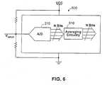
- circuit 600shows averaging circuitry 610.
- Averaging circuitry 610preferably receives a pre-determined number of digital addresses, averages the addresses, and derives an average. This digital address may be used similarly to the digital values described above.
- circuitry 610may be implemented in a suitable fashion as is well known to those skilled in the art.
- circuitry 610may be implemented as a register that; instead of averaging, stores three values. When any difference between the values is detected, the registers clears the values and starts storing the values again. An output is transmitted only when all three values match.
Landscapes
- Physics & Mathematics (AREA)
- Engineering & Computer Science (AREA)
- Spectroscopy & Molecular Physics (AREA)
- Computer Networks & Wireless Communication (AREA)
- Signal Processing (AREA)
- Computer Hardware Design (AREA)
- Computing Systems (AREA)
- General Engineering & Computer Science (AREA)
- Mathematical Physics (AREA)
- Analogue/Digital Conversion (AREA)
- Logic Circuits (AREA)
Abstract
Description
- A device in an electronic system may require a multi-bit digital address or number as an input. This number may represent an address on a serial bus, a configuration word, a system serial number, or some other information required by the device. Often this number is static, or changes infrequently during the operation of the device. In these circumstances-i.e., where this number is static or requires changes only infrequently - - this number is typically required at device startup.
- A simple way to input such a number to the device is to have several external pins, each corresponding to a bit of the input word. Each pin is tied to either a high or low value to represent the binary bits of the input word. While straightforward, this technique requires N external electrical connections, where N is the number of bits in the input word. If the device is an integrated circuit in a low-pin-count package, these input bits may consume most of the pins on the device, leaving few for other functionality. Thus, utilizing N pins, where each pin accepts one binary bit, limits the usefulness of the device and is, therefore, a sub-optimal design solution.
- Alternatively, the numeric input could also be programmed into the electronic device at the time of manufacture or system assembly, or could be transferred into the device through a single pin using a serial communication protocol. However, each of these methods requires significant additional complexity in the system architecture or manufacturing process.
- Thus, it would be desirable to provide circuits and methods that utilize a single pin to accept a single signal corresponding to a multi-bit digital address, number, or signal as required by the electronic device.
- It is an object of this invention to provide circuits and methods that utilize a single pin to accept a single signal corresponding to a multi-bit digital address, number, or signal as required by the electronic device.
- A method of configuring an electronic device via a single input pin of the electronic device is provided. The method preferably utilizes a first multi-bit digital address that was encoded as a first voltage signal. The method preferably includes receiving the first voltage signal at the single input pin of the electronic device. After the first voltage signal is received at the single input pin, the method further includes converting the first voltage signal received at the input pin into the first multi-bit digital address, and configuring the electronic device using the first multi-bit digital address.
- The objects and advantages of the invention will be apparent upon consideration of the following detailed description, taken in conjunction with the accompanying drawings, in which like reference characters refer to like parts throughout, and in which:
- FIG. 1 is a schematic diagram of a circuit according to the invention;
- FIG. 2A is a schematic diagram of a circuit according to the invention including an analog-to-digital converter according to the invention;
- FIG. 2B is a schematic diagram of a circuit according to the invention including an analog-to-digital converter having an internal voltage reference according to the invention;
- FIG. 3 is a schematic diagram of a circuit according to the invention that verifies the input voltage;
- FIG. 4 is a schematic diagram of a circuit according to the invention including a digital comparator;
- FIG. 5 is a schematic diagram of a circuit according to the invention including an averaging circuit; and
- FIG. 6 is another schematic diagram of a circuit according to the invention including an averaging circuit.
- Circuits and methods according to the invention preferably include inputting a single voltage signal, preferably via a single pin, corresponding to a multi-bit digital value. The digital value preferably includes a pre-determined number of bits.
- In one embodiment, a device which utilizes circuits and methods according to the invention preferably includes a power supply connection, a ground connection, each of which are connected to the device at respective input pins, and a third input pin. Other I/O pins may also be required for the device to function according to the individual requirements of the device.
- In the device according to the invention, a specific voltage is applied to the input pin. The voltage preferably corresponds,.according to a pre-determined protocol, to a multi-bit digital signal. This voltage is then, in turn, converted by an analog-to-digital converter or other suitable circuitry into the multi-bit digital input signal required by the device. Thus, the signal transferred to the single input voltage at the pin sets the desired multi-bit digital input signal for the electronic device. Furthermore, according to the invention, each of the several bits, which are encoded within the voltage signal, are programmed into the device substantially simultaneously, thereby reducing the time to program the multi-bit digital input signal.
- The desired multi-bit digital input signal may be represented at the input to the device by a voltage which is a pre-determined, preferably fixed, fraction or ratio of the total power supply voltage, or it may be referenced to an absolute voltage standard or reference. This fraction or ratio may be converted into the required multi-bit digital input signal. Further details of the invention will be explained below with respect to FIGS. 1-5.
- FIG. 1 shows an embodiment of a
device 100 according to the invention that includes a power supply, Vcc, a ground pin and aninput pin 110.Device 100 may also include other I/O pins 120 for transmitting digital or analog signals either to or fromdevice 100 as required bydevice 100. - The input voltage at
input pin 110 is preferably programmed by the value of theresistors input pin 110 is a fixed percentage of the voltage between the Vcc and ground pins. Device 100 may be utilized in a device that requires a 2-bit digital number as an input. In such a system, "00" may preferably correspond to an input voltage between 0% and 25% of the power-to-ground voltage, "01" may preferably correspond to an input voltage between 25% to 50%, "10" to 50% to 75%, and "11" to 75% to 100%. The determination of the range of percentages in which the voltage falls may preferably be obtained using a number or group of different comparators (not shown) in the electronic device, as is known in the art, in order to accurately determine the value (or range) of the incoming voltage. Once the value (or range) is determined, it may then be transferred as a single voltage -- e.g., from the midpoint of the range -- to an analog-to-digital converter (as shown in FIGS. 2A and 2B) in order to derive the multi-bit digital address.- This concept can be extended to almost any number of percentages, numbers and/or steps, with the limit set by the accuracy of the internal sensing scheme. The limit may also be set by the available values and precision of
resistors resistors - The voltage ranges at the input pin that correspond to individual digital values can be evenly sized and spaced across the available voltage range. Alternatively, the voltage ranges at the input pin can have unequal sizes and spaces.
- Equal-sized/spaced ranges ease calculation of error tolerances and are conceptually simpler. With an equal-sized scheme, conventional 10% margin-for-error resistors may be used to generate 2 input bits or 4 possible numeric inputs (as described above with respect to FIG. 1) without the risk of resistor tolerance error causing a false input reading. 1% error resistors may be used to generate 5 bits or 32 possible inputs, and 0.1% resistors may be used to generate up to 8 bits or 256 inputs.
- Unequal-sized/spaced ranges can also be used to simplify the choice of external resistor values. This may be accomplished by choosing the range of the resistors so that a resistor divider is used with two fixed resistors or with one resistor value fixed and one resistor value varying in a linear manner may be used to select the desired input. The resistor value may preferably vary, or be adjustable, in known incremental values. Or, in an alternative embodiment, the resistor value may vary, or be adjustable, in a smoothed fashion.
- It is possible that noise at the input pin or at the power supplies can cause intermittent erroneous readings, especially when several bits are being programmed and the separation between adjacent steps is small. Additional circuitry can be added to take multiple readings at the input pin, and either arithmetically average the readings or require a sequence of several identical readings before a valid input is recognized. Circuitry to implement additional readings and/or averaging will be shown in detail below with respect to FIGS. 3 and 4.
- FIG. 2A shows another embodiment of the invention in which
device 200 may communicate over a serial digital interface bus, such as an I2C bus made by Phillips Electronics of the Netherlands, and notifies and/or identifies the central processing unit of a unique address to write data to, to transmit data from, or to configuredevice 200. The selected address that should be identified to receive and/or transmit the signal may be programmed as a resistor-divided voltage intoresistors - In one embodiment of the invention, the resistors may be individually chosen for each of a set of components along a serial bus -- e.g., a fan control chip, a voltage monitor device for a battery or a device to control contrast for a screen voltage monitor -- such that each component receives a preferably user-determined, unique voltage which may then be converted into a digital address as the device's unique address. This voltage may identify the device to the device itself by a particular address. This identity may be static for the operative cycle-i.e., as long as the chip is powered up -- of the chip. When a microcontroller or other suitable processor uses the serial bus to communicate with the devices along the bus during operation of the chip, the microcontroller may refer to the device by the address identified to the device by the choice of resistors in the resistor divider. This embodiment obtains the advantage that each of the devices on the serial bus may be identified by resistor choice as opposed to assigning each chip a unique design. Thus, the chip manufacturer may be able to produce a single chip to fit various system requirements -- e.g., various voltage levels as required by differing systems. The chip is then customized by the individual user merely by adding resistors as required by his system requirements.
- For example, a single fan control chip may be implemented in systems where the fan may use different addresses. These different addresses may be identified in each individual system according to the resistor choice of the user. Therefore, the fan chip maker requires only a single chip and his inventory, as well as the inventory of a user with various systems, is substantially simplified.
- As described above, one or both of
resistors Electronic device 200 preferably requires internal circuitry to convert the voltage at the input pin into a digital address. This circuitry may be implemented in a number of suitable ways.Device 200 may preferably include analog-to-digital converter 210 to convert the voltage at the input pin into a digital value. Analog-to-digital converter 210 may preferably have sufficient resolution that it can be set to accurately read and convert the voltage at the input pin. Analog-to-digital converter 210 may also be coupled to register 220.Register 220 may,preferably store the resulting value for later comparison with other incoming address words or for transferring the value to a system controller (not shown).- Analog-to-
digital converter 210 may also preferably be coupled between Vcc and ground such that the scale of digital addresses produced by analog-to-digital converter 210 varies proportionally to changes in Vcc. This is required because Vcc may change during the operation ofdevice 200 and alter the voltage seen byinput pin 110. When analog-to-digital converter 210 is bound by Vcc and ground in this way, the digital addresses that analog-to-digital converter 210 provides are accurate even though Vcc may change. - Once
device 200 has received the input voltage and converted it into a multi-bit digital value, it may use this value to identify an address indevice 200. When this address is identified,device 200 may perform any suitable action with the address. Examples of such suitable actions are the outputting of the value stored at the identified address to another portion ofdevice 200, or even outputting the value offdevice 200 to another device. Alternatively, the address and/or the value at the address may be stored for later use or reference. - In a device that uses a serial bus, bits and/or addresses are often shifted into a register prior to the time when the device is required to recognize the address. When a serial bus, such as the I2C bus, is used, the components that are coupled to the bus require a unique address in order to interpret the communication from the bus. The address allows the component to be alerted when a communication directed to the component is being transmitted along the bus. The microcontroller first transfers the address along the bus. Then, the microcontroller transfers the information. In FIG. 2, the address for the particular component may be communicated to
electronic device 200 viainput pin 110 by the resistor divider formed byresistors electronic device 200. Once addressed,electronic device 200 may be prepared to accept communication from the microcontroller. - In another alternative embodiment, the address may be used as a configuration word to configure
device 200 in some suitable fashion -- e.g., to informdevice 200 that it should act as memory device, a signal processor, any other suitable device, or to informdevice 200 that is has a particular address to be on alert for when instructions are generated from the serial bus. The foregoing are only examples of the use of the identified address, and the value located therein, and are not meant to be exhaustive or to limit the scope of the invention with respect to the use of the multi-bit digital value derived from the input voltage. - Analog-to-
digital converter 210 may also preferably be coupled between Vcc and ground such that the scale of digital addresses produced by analog-to-digital converter 210 remains independent of changes in Vcc. The scale of digital addresses is independent because it also is based on an analog scale that uses as a high (or low) end reference voltage. This extra functionality is required because Vcc may change during the operation ofdevice 200 and alter the voltage seen byinput pin 110. When analog-to-digital converter 210 is bound by reference voltage Vcc and ground in this way, the digital addresses that analog-to-digital converter 210 provides are maintained accurately even though Vcc may change. - FIG. 2B shows another embodiment of a device 250 according to the invention. The main difference between
device 200 and device 250 is that the reference voltage for analog-to-digital converter 210, and for the resistor-divider including resistors device 200 and internally in device 250. Generating the reference voltage internally mitigates the error that occurs indevice 200 between the mismatching of capacitances generated atinput pin 110 and at the coupling of Vcc to analog-to-digital converter 210. - In another embodiment of the invention,
device 200 shown in FIG. 2A or 2B may be configured as an analog voltage monitor. One purpose of a voltage monitor may be to determine whether a voltage at a particular I/O pin, or an internal voltage, is below, at, or above a pre-determined voltage or range of voltages. This function may be accomplished using a voltage monitor. - In the circuit shown in FIG. 2, the input at
pin 110 may be a pre-determined voltage. This voltage is preferably converted into a digital address by analog-to-digital converter 210. Then, the digital address may be stored inregister 220 and finally transferred or conveyed to the system controller. According to this embodiment of the invention, the stored value may be used to configure the voltage monitor. One aspect of the configuration may be to define the voltage level, or range of levels, of the monitor. Thus,device 200 may be configured to perform different functions, or to perform the same function -- i.e., to monitor voltage -- at different levels or ranges of levels. These different levels or ranges of levels are typically referred to as the trip level or levels of the voltage monitor. - FIG. 3 shows another embodiment of a
device 300 according to the invention. This embodiment may be used to sample the input voltage multiple times and to validate the address provided by the multiple samples. This embodiment is particularly advantageous in a system that uses a serial bus and requires the identification of an address. Device 300 preferably includes additional components such as a digital-to-analog converter 310 for re-converting the digital address stored in theregister 220 into a voltage, and awindow comparator 330 for determining whether the two representative voltages, and, consequentially, the two derived digital values, are substantially the same.Device 300 preferably operates as follows. When a first voltage is applied toinput pin 110, this voltage may preferably be converted by analog-to-digital converter 210 to a digital address. This digital address may preferably be stored inregister 220. When the digital address is required for a comparison to a new input voltage, the digital address stored inregister 220 may be output to digital-to-analog converter 310.- Then, the voltage from
converter 310 may be conveyed to awindow comparator 330. The references values, Vref1 and Vref2, for the window comparator may preferably be obtained by converting the stored digital value into an analog voltage and proportionally adjusting the re-converted analog voltage up and down by some pre-determined fraction -- e.g., byvoltage multiplier 340 andvoltage divider 350 -- to form a voltage range between the higher and the lower voltage values about the voltage from digital-to-analog converter 310. These two voltages may then be used to set a comparison range or "window" in which a second input voltage may be verified. This window is preferably small enough such that the acceptance level ofwindow comparator 330 is narrower than the separation between adjacent input levels. In this particular embodiment of the invention,XOR gate 360 may preferably provide a high signal when the second voltage is within the verification window (or validation) window. - Prior to the input of the second analog voltage, the output of digital-to-
analog converter 310 may preferably be set such that the first voltage is not validated against the start-up output of digital-to-analog converter 210. Therefore,window comparator 330 preferably provides an "invalid" output afterdevice 300 receives the initial voltage because the input frominput pin 110 does not match the input fromregister 220 via digital-to-analog converter 310. The "invalid" output indicates that the input voltage signal has not been verified by being matched to the previously input voltage signal. Thereafter, the input value from analog-to-digital converter 210 is stored inregister 220. - When a second voltage is applied to
input pin 110, the second voltage may be compared to the range established by up-multiplier 340 and down-divider 350. This comparison validates the first and second voltage signals, and, consequently the first and second digital signals. Preferably, this comparison should be implemented in accordance with a suitable timing scheme such that the second signal does not overwrite the first signal inregister 220 before the comparison is made. - If the two addresses are substantially the same, then window comparator may preferably output a "valid" response -- i.e., the input voltage has been verified.
Device 300 may preferably utilize the address either as derived from the analog-to-digital converter 210 and/or fromregister 220 because, after the voltages have been validated, both of these values are substantially the same. - The process of validating the input voltage, and, consequently, the input address, may be repeated as many times as necessary to insure correct signal transmission and reception.
- Thus,
device 300 may preferably provide a pass/no-pass comparison of the multi-bit digital signal (or address word) without requiring an analog-to-digital conversion of the incoming signal followed by an arithmetic comparison. It should be noted that a circuit includingwindow comparator 330 is only one embodiment of a circuit for validating the incoming voltage signal. Other suitable circuitry or methodology may be used for this function. - Alternatively, the comparison may be implemented by comparing the first digital signal output from
register 220 to a digital signal output from analog-to-digital converter 210 using a digital comparator. These digital signals may be compared when the timing of the output ofregister 220 coincides with the timing of the output of analog-to-digital converter 210. - One possible implementation of a circuit implementing a digital comparator that is suitable for comparing the two digital signals is shown in FIG. 4.
Digital comparator 410, which preferably includes XOR andOR logic gates 420, may preferably be implemented to compare the output of analog-to-digital converter 210 with the output ofregister 220. As mentioned above, a suitable timing scheme is required for implementation ofdigital comparator 410. - In an alternative embodiment,
circuit 500shows averaging circuitry 510. Averagingcircuitry 510 preferably receives a pre-determined number of voltage values, averages the values, and derives an average voltage. This voltage may then be converted into a digital value by analog-to-digital converter 210. This digital value may be used similarly to the digital values described above. Preferably the averaging circuitry provides the corrected voltage to the rest of the circuitry. - The actual averaging function of averaging
circuitry 510 may be implemented in a suitable fashion as is well known to those skilled in the art. - In yet another alternative embodiment,
circuit 600shows averaging circuitry 610. Averagingcircuitry 610 preferably receives a pre-determined number of digital addresses, averages the addresses, and derives an average. This digital address may be used similarly to the digital values described above. - The actual averaging function of averaging
circuitry 610 may be implemented in a suitable fashion as is well known to those skilled in the art. In another embodiment,circuitry 610 may be implemented as a register that; instead of averaging, stores three values. When any difference between the values is detected, the registers clears the values and starts storing the values again. An output is transmitted only when all three values match. - Thus, electronic devices and methods for transmitting a multi-bit digital signal via a single pin are provided. Persons skilled in the art will appreciate that the present invention can be practiced by other than the described embodiments, which are presented for purposes of illustration rather than of limitation, and the present invention is limited only by the claims which follow.
Claims (8)
- A method of configuring an electronic device using a first multi-bit digital address, the first multi-bit digital address being encoded as a first voltage signal, the method comprising:receiving the first voltage signal at a single input pin of the electronic device;after the first voltage signal is received at the single input pin, converting the first voltage signal received at the input pin into the first multi-bit digital address; andconfiguring the electronic device using the first multi-bit digital address.
- The method of claim 1 further comprising maintaining the device as responsive to a bus communication signal following a transmission of a bus address signal including the first multi-bit digital address.
- The method of claim 1 or 2 further comprising:receiving a second multi-bit digital address that has been encoded as a second voltage signal at the first input pin or at a second input pin;converting the second voltage signal to obtain a verification address; andverifying the verification address by comparing the first multi-bit digital address to the verification address.
- The method of claim 1, 2 or 3, further comprising:receiving a second voltage signal at the first input pin or a second input pin;converting the second voltage signal into a verification voltage range; anddetermining whether the first voltage signal is within the verification voltage range.
- The method of any one of claims 1 to 4, the converting further comprising converting integrally to the electronic device.
- The method of any one of claims 1 to 5, the configuring further comprising configuring the electronic device as a voltage monitor using the first digital address.
- The method of claim 5 or 6, the configuring further comprising configuring the trip points of the voltage monitor using the first digital address.
- The method of any one of claims 1 to 7, further comprising referencing the converting to a reference value that is substantially equal to a reference value used to encode the first multi-bit digital signal as the first voltage signal.
Applications Claiming Priority (3)
| Application Number | Priority Date | Filing Date | Title |
|---|---|---|---|
| US10/124,658US6967591B1 (en) | 2002-04-15 | 2002-04-15 | Multi-bit digital input using a single pin |
| EP03008073AEP1355426B1 (en) | 2002-04-15 | 2003-04-14 | Multi-bit digital input using a single pin |
| EP05018493.6AEP1608070B1 (en) | 2002-04-15 | 2003-04-14 | Multi-bit digital input using a single pin |
Related Parent Applications (3)
| Application Number | Title | Priority Date | Filing Date |
|---|---|---|---|
| EP03008073ADivisionEP1355426B1 (en) | 2002-04-15 | 2003-04-14 | Multi-bit digital input using a single pin |
| EP05018493.6ADivisionEP1608070B1 (en) | 2002-04-15 | 2003-04-14 | Multi-bit digital input using a single pin |
| EP05018493.6ADivision-IntoEP1608070B1 (en) | 2002-04-15 | 2003-04-14 | Multi-bit digital input using a single pin |
Publications (2)
| Publication Number | Publication Date |
|---|---|
| EP1696568A1true EP1696568A1 (en) | 2006-08-30 |
| EP1696568B1 EP1696568B1 (en) | 2017-11-22 |
Family
ID=28674695
Family Applications (3)
| Application Number | Title | Priority Date | Filing Date |
|---|---|---|---|
| EP06005886.4AExpired - LifetimeEP1696568B1 (en) | 2002-04-15 | 2003-04-14 | Multi-bit digital input using a single pin |
| EP05018493.6AExpired - LifetimeEP1608070B1 (en) | 2002-04-15 | 2003-04-14 | Multi-bit digital input using a single pin |
| EP03008073AExpired - LifetimeEP1355426B1 (en) | 2002-04-15 | 2003-04-14 | Multi-bit digital input using a single pin |
Family Applications After (2)
| Application Number | Title | Priority Date | Filing Date |
|---|---|---|---|
| EP05018493.6AExpired - LifetimeEP1608070B1 (en) | 2002-04-15 | 2003-04-14 | Multi-bit digital input using a single pin |
| EP03008073AExpired - LifetimeEP1355426B1 (en) | 2002-04-15 | 2003-04-14 | Multi-bit digital input using a single pin |
Country Status (3)
| Country | Link |
|---|---|
| US (3) | US6967591B1 (en) |
| EP (3) | EP1696568B1 (en) |
| DE (1) | DE60317599T2 (en) |
Cited By (1)
| Publication number | Priority date | Publication date | Assignee | Title |
|---|---|---|---|---|
| US11526455B2 (en)* | 2020-11-06 | 2022-12-13 | Samsung Electro-Mechanics Co., Ltd. | Slave devices and slave apparatus for designating address using a single pin |
Families Citing this family (16)
| Publication number | Priority date | Publication date | Assignee | Title |
|---|---|---|---|---|
| US7139352B2 (en)* | 1999-12-28 | 2006-11-21 | Kabushiki Kaisha Toshiba | Reactivity control rod for core |
| DE10323012B4 (en) | 2003-05-21 | 2005-06-02 | Austriamicrosystems Ag | Programmable integrated circuit and method of programming an integrated circuit |
| DE102004017863B4 (en)* | 2004-04-13 | 2014-09-25 | Qimonda Ag | Circuit and method for determining a reference level for such a circuit |
| US7376020B2 (en)* | 2005-12-13 | 2008-05-20 | Microchip Technology Incorporated | Memory using a single-node data, address and control bus |
| US20080278346A1 (en)* | 2007-05-11 | 2008-11-13 | Eftimie Sabin A | Single-Pin Multi-Bit Digital Circuit Configuration |
| US7827330B2 (en) | 2007-07-27 | 2010-11-02 | Microchip Technology Incorporated | Configuring multi-bit slave addressing on a serial bus using a single external connection |
| US7816907B2 (en)* | 2008-04-23 | 2010-10-19 | Lantiq Deutschland Gmbh | Integrated circuit with a measuring circuit and method of configuring an integrated circuit with a measuring circuit |
| US20100327194A1 (en)* | 2009-06-26 | 2010-12-30 | Jian Xu | Multi-bit use of a standard optocoupler |
| CN201628954U (en)* | 2009-11-18 | 2010-11-10 | 华为终端有限公司 | Electronic product identification device and electronic equipment |
| TWI402716B (en)* | 2010-02-04 | 2013-07-21 | Novatek Microelectronics Corp | Key activity detection system and method thereof |
| US9037766B2 (en)* | 2011-11-18 | 2015-05-19 | Fairchild Semiconductor Corporation | Pin selectable I2C slave addresses |
| DE102011120695B4 (en)* | 2011-12-09 | 2015-01-15 | Brose Fahrzeugteile Gmbh & Co. Kommanditgesellschaft, Hallstadt | Control device and method for its monitoring |
| CN106533488A (en) | 2015-09-11 | 2017-03-22 | 天工方案公司 | Device including multi-mode input pad |
| US10519614B2 (en)* | 2017-06-26 | 2019-12-31 | Teh Boeing Company | System and method for automated deployment of a passenger boarding bridge |
| US10561232B2 (en)* | 2017-06-27 | 2020-02-18 | Colgate-Palmolive Company | Oral care implement |
| CN116450028B (en)* | 2023-06-19 | 2023-09-15 | 西安矽源半导体有限公司 | A method and system for configuring multi-bit device addresses on a single port |
Citations (4)
| Publication number | Priority date | Publication date | Assignee | Title |
|---|---|---|---|---|
| US4604692A (en)* | 1981-12-29 | 1986-08-05 | Fujitsu Limited | Operation mode setting system for a microprocessor |
| JPH08105942A (en)* | 1994-10-05 | 1996-04-23 | Kawasaki Steel Corp | Semiconductor integrated circuit |
| US5737235A (en)* | 1995-05-02 | 1998-04-07 | Xilinx Inc | FPGA with parallel and serial user interfaces |
| WO1999043003A1 (en)* | 1998-02-23 | 1999-08-26 | Micron Technology, Inc. | Multi-level data through a single input/output pin |
Family Cites Families (8)
| Publication number | Priority date | Publication date | Assignee | Title |
|---|---|---|---|---|
| US6169503B1 (en)* | 1998-09-23 | 2001-01-02 | Sandisk Corporation | Programmable arrays for data conversions between analog and digital |
| US6369738B1 (en)* | 1999-08-17 | 2002-04-09 | Eric Swanson | Time domain/frequency domain data converter with data ready feature |
| US6564278B1 (en)* | 1999-10-21 | 2003-05-13 | Ulysses Esd, Inc. | System and method for obtaining board address information |
| US7024539B2 (en)* | 2000-07-17 | 2006-04-04 | Silicon Laboratories Inc. | Resistor identification configuration circuitry and associated method |
| US6504347B1 (en)* | 2001-04-02 | 2003-01-07 | National Seminconductor Corporation | Apparatus for sub-regulating and sensing an input voltage with minimum connections |
| US7036061B2 (en)* | 2001-08-28 | 2006-04-25 | Intel Corporation | Structural input levels testing using on-die levels generators |
| US6922071B2 (en)* | 2002-12-27 | 2005-07-26 | Intel Corporation | Setting multiple chip parameters using one IC terminal |
| US7102394B1 (en)* | 2005-09-27 | 2006-09-05 | Micrel, Inc. | Programming and control of an integrated circuit using an externally connected resistor network |
- 2002
- 2002-04-15USUS10/124,658patent/US6967591B1/ennot_activeExpired - Lifetime
- 2003
- 2003-04-14EPEP06005886.4Apatent/EP1696568B1/ennot_activeExpired - Lifetime
- 2003-04-14EPEP05018493.6Apatent/EP1608070B1/ennot_activeExpired - Lifetime
- 2003-04-14EPEP03008073Apatent/EP1355426B1/ennot_activeExpired - Lifetime
- 2003-04-14DEDE60317599Tpatent/DE60317599T2/ennot_activeExpired - Lifetime
- 2005
- 2005-09-09USUS11/222,996patent/US7119714B2/ennot_activeExpired - Lifetime
- 2005-09-09USUS11/223,188patent/US7239251B2/ennot_activeExpired - Lifetime
Patent Citations (4)
| Publication number | Priority date | Publication date | Assignee | Title |
|---|---|---|---|---|
| US4604692A (en)* | 1981-12-29 | 1986-08-05 | Fujitsu Limited | Operation mode setting system for a microprocessor |
| JPH08105942A (en)* | 1994-10-05 | 1996-04-23 | Kawasaki Steel Corp | Semiconductor integrated circuit |
| US5737235A (en)* | 1995-05-02 | 1998-04-07 | Xilinx Inc | FPGA with parallel and serial user interfaces |
| WO1999043003A1 (en)* | 1998-02-23 | 1999-08-26 | Micron Technology, Inc. | Multi-level data through a single input/output pin |
Non-Patent Citations (1)
| Title |
|---|
| PATENT ABSTRACTS OF JAPAN vol. 1996, no. 08 30 August 1996 (1996-08-30)* |
Cited By (1)
| Publication number | Priority date | Publication date | Assignee | Title |
|---|---|---|---|---|
| US11526455B2 (en)* | 2020-11-06 | 2022-12-13 | Samsung Electro-Mechanics Co., Ltd. | Slave devices and slave apparatus for designating address using a single pin |
Also Published As
| Publication number | Publication date |
|---|---|
| EP1355426A1 (en) | 2003-10-22 |
| EP1608070A2 (en) | 2005-12-21 |
| US7119714B2 (en) | 2006-10-10 |
| DE60317599T2 (en) | 2008-03-13 |
| EP1355426B1 (en) | 2007-11-21 |
| DE60317599D1 (en) | 2008-01-03 |
| US6967591B1 (en) | 2005-11-22 |
| US20060007018A1 (en) | 2006-01-12 |
| EP1608070A3 (en) | 2006-01-11 |
| US20060007019A1 (en) | 2006-01-12 |
| EP1696568B1 (en) | 2017-11-22 |
| US7239251B2 (en) | 2007-07-03 |
| EP1608070B1 (en) | 2017-11-29 |
Similar Documents
| Publication | Publication Date | Title |
|---|---|---|
| EP1608070B1 (en) | Multi-bit digital input using a single pin | |
| US7269043B2 (en) | Memory module and impedance calibration method of semiconductor memory device | |
| US9213396B1 (en) | Methods and apparatus for setting the address of a module using a clock | |
| US6734702B1 (en) | Impedance calibration circuit | |
| US9298908B1 (en) | Methods and apparatus for setting the address of a module using a voltage | |
| US20050160334A1 (en) | Apparatus for detecting A/D converter abnormality | |
| CN111147080B (en) | Integrated circuit and method for transmitting data | |
| CN112636717B (en) | Impedance calibration circuit and method | |
| US6608582B2 (en) | A/D conversion using a variable offset comparator | |
| US6617918B2 (en) | Multi-level receiver circuit with digital output using a variable offset comparator | |
| US6653893B2 (en) | Voltage margin testing of a transmission line analog signal using a variable offset comparator in a data receiver circuit | |
| KR20070088845A (en) | Impedance calibration method of memory module and semiconductor devices included in memory module | |
| US5646609A (en) | Circuit and method for selecting a circuit module | |
| CN214205481U (en) | Impedance Calibration Circuit | |
| JP4000629B2 (en) | Sensor with adjustment function | |
| JP2002290236A (en) | Analog / digital conversion circuit | |
| JP3945364B2 (en) | Individual identification code creation method and circuit | |
| WO2007029449A1 (en) | Data transmission system | |
| EP1414206A1 (en) | Semiconductor device and data transfer system | |
| EP1299883A2 (en) | Simple chip identification | |
| JP2624215B2 (en) | Option board identification device | |
| JPH11288330A (en) | Integrated circuit with setting function | |
| US20060002493A1 (en) | Method and device for generating a duty cycle related output signal |
Legal Events
| Date | Code | Title | Description |
|---|---|---|---|
| PUAI | Public reference made under article 153(3) epc to a published international application that has entered the european phase | Free format text:ORIGINAL CODE: 0009012 | |
| AC | Divisional application: reference to earlier application | Ref document number:1608070 Country of ref document:EP Kind code of ref document:P Ref document number:1355426 Country of ref document:EP Kind code of ref document:P | |
| AK | Designated contracting states | Kind code of ref document:A1 Designated state(s):AT BE BG CH CY CZ DE DK EE ES FI FR GB GR HU IE IT LI LU MC NL PT RO SE SI SK TR | |
| 17P | Request for examination filed | Effective date:20061108 | |
| 17Q | First examination report despatched | Effective date:20061211 | |
| AKX | Designation fees paid | Designated state(s):AT BE BG CH CY CZ DE DK EE ES FI FR GB GR HU IE IT LI LU MC NL PT RO SE SI SK TR | |
| RAP1 | Party data changed (applicant data changed or rights of an application transferred) | Owner name:LINEAR TECHNOLOGY CORPORATION | |
| REG | Reference to a national code | Ref country code:DE Ref legal event code:R079 Ref document number:60350792 Country of ref document:DE Free format text:PREVIOUS MAIN CLASS: H03K0019173000 Ipc:H04L0025490000 | |
| RIC1 | Information provided on ipc code assigned before grant | Ipc:H03K 19/173 20060101ALI20170328BHEP Ipc:H04L 25/49 20060101AFI20170328BHEP | |
| GRAP | Despatch of communication of intention to grant a patent | Free format text:ORIGINAL CODE: EPIDOSNIGR1 | |
| INTG | Intention to grant announced | Effective date:20170508 | |
| GRAS | Grant fee paid | Free format text:ORIGINAL CODE: EPIDOSNIGR3 | |
| GRAJ | Information related to disapproval of communication of intention to grant by the applicant or resumption of examination proceedings by the epo deleted | Free format text:ORIGINAL CODE: EPIDOSDIGR1 | |
| GRAL | Information related to payment of fee for publishing/printing deleted | Free format text:ORIGINAL CODE: EPIDOSDIGR3 | |
| GRAR | Information related to intention to grant a patent recorded | Free format text:ORIGINAL CODE: EPIDOSNIGR71 | |
| GRAA | (expected) grant | Free format text:ORIGINAL CODE: 0009210 | |
| INTC | Intention to grant announced (deleted) | ||
| REG | Reference to a national code | Ref country code:DE Ref legal event code:R081 Ref document number:60350792 Country of ref document:DE Owner name:ANALOG DEVICES INTERNATIONAL UNLIMITED COMPANY, IE Free format text:FORMER OWNER: LINEAR TECHNOLOGY CORP., MILPITAS, CALIF., US | |
| AC | Divisional application: reference to earlier application | Ref document number:1608070 Country of ref document:EP Kind code of ref document:P Ref document number:1355426 Country of ref document:EP Kind code of ref document:P | |
| AK | Designated contracting states | Kind code of ref document:B1 Designated state(s):AT BE BG CH CY CZ DE DK EE ES FI FR GB GR HU IE IT LI LU MC NL PT RO SE SI SK TR | |
| INTG | Intention to grant announced | Effective date:20171018 | |
| REG | Reference to a national code | Ref country code:GB Ref legal event code:FG4D | |
| REG | Reference to a national code | Ref country code:CH Ref legal event code:EP | |
| REG | Reference to a national code | Ref country code:IE Ref legal event code:FG4D | |
| REG | Reference to a national code | Ref country code:AT Ref legal event code:REF Ref document number:949363 Country of ref document:AT Kind code of ref document:T Effective date:20171215 | |
| REG | Reference to a national code | Ref country code:DE Ref legal event code:R096 Ref document number:60350792 Country of ref document:DE | |
| REG | Reference to a national code | Ref country code:NL Ref legal event code:FP | |
| REG | Reference to a national code | Ref country code:FR Ref legal event code:PLFP Year of fee payment:16 | |
| REG | Reference to a national code | Ref country code:AT Ref legal event code:MK05 Ref document number:949363 Country of ref document:AT Kind code of ref document:T Effective date:20171122 | |
| PG25 | Lapsed in a contracting state [announced via postgrant information from national office to epo] | Ref country code:FI Free format text:LAPSE BECAUSE OF FAILURE TO SUBMIT A TRANSLATION OF THE DESCRIPTION OR TO PAY THE FEE WITHIN THE PRESCRIBED TIME-LIMIT Effective date:20171122 Ref country code:SE Free format text:LAPSE BECAUSE OF FAILURE TO SUBMIT A TRANSLATION OF THE DESCRIPTION OR TO PAY THE FEE WITHIN THE PRESCRIBED TIME-LIMIT Effective date:20171122 Ref country code:ES Free format text:LAPSE BECAUSE OF FAILURE TO SUBMIT A TRANSLATION OF THE DESCRIPTION OR TO PAY THE FEE WITHIN THE PRESCRIBED TIME-LIMIT Effective date:20171122 | |
| PG25 | Lapsed in a contracting state [announced via postgrant information from national office to epo] | Ref country code:AT Free format text:LAPSE BECAUSE OF FAILURE TO SUBMIT A TRANSLATION OF THE DESCRIPTION OR TO PAY THE FEE WITHIN THE PRESCRIBED TIME-LIMIT Effective date:20171122 Ref country code:BG Free format text:LAPSE BECAUSE OF FAILURE TO SUBMIT A TRANSLATION OF THE DESCRIPTION OR TO PAY THE FEE WITHIN THE PRESCRIBED TIME-LIMIT Effective date:20180222 Ref country code:GR Free format text:LAPSE BECAUSE OF FAILURE TO SUBMIT A TRANSLATION OF THE DESCRIPTION OR TO PAY THE FEE WITHIN THE PRESCRIBED TIME-LIMIT Effective date:20180223 | |
| PG25 | Lapsed in a contracting state [announced via postgrant information from national office to epo] | Ref country code:SK Free format text:LAPSE BECAUSE OF FAILURE TO SUBMIT A TRANSLATION OF THE DESCRIPTION OR TO PAY THE FEE WITHIN THE PRESCRIBED TIME-LIMIT Effective date:20171122 Ref country code:DK Free format text:LAPSE BECAUSE OF FAILURE TO SUBMIT A TRANSLATION OF THE DESCRIPTION OR TO PAY THE FEE WITHIN THE PRESCRIBED TIME-LIMIT Effective date:20171122 Ref country code:EE Free format text:LAPSE BECAUSE OF FAILURE TO SUBMIT A TRANSLATION OF THE DESCRIPTION OR TO PAY THE FEE WITHIN THE PRESCRIBED TIME-LIMIT Effective date:20171122 Ref country code:CY Free format text:LAPSE BECAUSE OF FAILURE TO SUBMIT A TRANSLATION OF THE DESCRIPTION OR TO PAY THE FEE WITHIN THE PRESCRIBED TIME-LIMIT Effective date:20171122 Ref country code:CZ Free format text:LAPSE BECAUSE OF FAILURE TO SUBMIT A TRANSLATION OF THE DESCRIPTION OR TO PAY THE FEE WITHIN THE PRESCRIBED TIME-LIMIT Effective date:20171122 | |
| REG | Reference to a national code | Ref country code:DE Ref legal event code:R097 Ref document number:60350792 Country of ref document:DE | |
| PG25 | Lapsed in a contracting state [announced via postgrant information from national office to epo] | Ref country code:RO Free format text:LAPSE BECAUSE OF FAILURE TO SUBMIT A TRANSLATION OF THE DESCRIPTION OR TO PAY THE FEE WITHIN THE PRESCRIBED TIME-LIMIT Effective date:20171122 | |
| PLBE | No opposition filed within time limit | Free format text:ORIGINAL CODE: 0009261 | |
| STAA | Information on the status of an ep patent application or granted ep patent | Free format text:STATUS: NO OPPOSITION FILED WITHIN TIME LIMIT | |
| 26N | No opposition filed | Effective date:20180823 | |
| PG25 | Lapsed in a contracting state [announced via postgrant information from national office to epo] | Ref country code:MC Free format text:LAPSE BECAUSE OF FAILURE TO SUBMIT A TRANSLATION OF THE DESCRIPTION OR TO PAY THE FEE WITHIN THE PRESCRIBED TIME-LIMIT Effective date:20171122 Ref country code:SI Free format text:LAPSE BECAUSE OF FAILURE TO SUBMIT A TRANSLATION OF THE DESCRIPTION OR TO PAY THE FEE WITHIN THE PRESCRIBED TIME-LIMIT Effective date:20171122 | |
| REG | Reference to a national code | Ref country code:CH Ref legal event code:PL | |
| REG | Reference to a national code | Ref country code:BE Ref legal event code:MM Effective date:20180430 | |
| REG | Reference to a national code | Ref country code:IE Ref legal event code:MM4A | |
| PG25 | Lapsed in a contracting state [announced via postgrant information from national office to epo] | Ref country code:LU Free format text:LAPSE BECAUSE OF NON-PAYMENT OF DUE FEES Effective date:20180414 | |
| PG25 | Lapsed in a contracting state [announced via postgrant information from national office to epo] | Ref country code:CH Free format text:LAPSE BECAUSE OF NON-PAYMENT OF DUE FEES Effective date:20180430 Ref country code:LI Free format text:LAPSE BECAUSE OF NON-PAYMENT OF DUE FEES Effective date:20180430 Ref country code:BE Free format text:LAPSE BECAUSE OF NON-PAYMENT OF DUE FEES Effective date:20180430 | |
| PG25 | Lapsed in a contracting state [announced via postgrant information from national office to epo] | Ref country code:IE Free format text:LAPSE BECAUSE OF NON-PAYMENT OF DUE FEES Effective date:20180414 | |
| PG25 | Lapsed in a contracting state [announced via postgrant information from national office to epo] | Ref country code:TR Free format text:LAPSE BECAUSE OF FAILURE TO SUBMIT A TRANSLATION OF THE DESCRIPTION OR TO PAY THE FEE WITHIN THE PRESCRIBED TIME-LIMIT Effective date:20171122 | |
| PG25 | Lapsed in a contracting state [announced via postgrant information from national office to epo] | Ref country code:HU Free format text:LAPSE BECAUSE OF FAILURE TO SUBMIT A TRANSLATION OF THE DESCRIPTION OR TO PAY THE FEE WITHIN THE PRESCRIBED TIME-LIMIT; INVALID AB INITIO Effective date:20030414 Ref country code:PT Free format text:LAPSE BECAUSE OF FAILURE TO SUBMIT A TRANSLATION OF THE DESCRIPTION OR TO PAY THE FEE WITHIN THE PRESCRIBED TIME-LIMIT Effective date:20171122 | |
| PGFP | Annual fee paid to national office [announced via postgrant information from national office to epo] | Ref country code:IT Payment date:20210323 Year of fee payment:19 Ref country code:NL Payment date:20210329 Year of fee payment:19 | |
| REG | Reference to a national code | Ref country code:DE Ref legal event code:R082 Ref document number:60350792 Country of ref document:DE Representative=s name:VOSSIUS & PARTNER PATENTANWAELTE RECHTSANWAELT, DE Ref country code:DE Ref legal event code:R081 Ref document number:60350792 Country of ref document:DE Owner name:ANALOG DEVICES INTERNATIONAL UNLIMITED COMPANY, IE Free format text:FORMER OWNER: LINEAR TECHNOLOGY CORP., MILPITAS, CALIF., US | |
| PGFP | Annual fee paid to national office [announced via postgrant information from national office to epo] | Ref country code:GB Payment date:20210324 Year of fee payment:19 | |
| PGFP | Annual fee paid to national office [announced via postgrant information from national office to epo] | Ref country code:DE Payment date:20210323 Year of fee payment:19 | |
| REG | Reference to a national code | Ref country code:NL Ref legal event code:PD Owner name:ANALOG DEVICES INTERNATIONAL UNLIMITED COMPANY; IE Free format text:DETAILS ASSIGNMENT: CHANGE OF OWNER(S), ASSIGNMENT; FORMER OWNER NAME: LINEAR TECHNOLOGY LLC Effective date:20211216 | |
| PGFP | Annual fee paid to national office [announced via postgrant information from national office to epo] | Ref country code:FR Payment date:20220323 Year of fee payment:20 | |
| REG | Reference to a national code | Ref country code:DE Ref legal event code:R119 Ref document number:60350792 Country of ref document:DE | |
| REG | Reference to a national code | Ref country code:NL Ref legal event code:MM Effective date:20220501 | |
| GBPC | Gb: european patent ceased through non-payment of renewal fee | Effective date:20220414 | |
| PG25 | Lapsed in a contracting state [announced via postgrant information from national office to epo] | Ref country code:NL Free format text:LAPSE BECAUSE OF NON-PAYMENT OF DUE FEES Effective date:20220501 Ref country code:GB Free format text:LAPSE BECAUSE OF NON-PAYMENT OF DUE FEES Effective date:20220414 Ref country code:DE Free format text:LAPSE BECAUSE OF NON-PAYMENT OF DUE FEES Effective date:20221103 | |
| PG25 | Lapsed in a contracting state [announced via postgrant information from national office to epo] | Ref country code:IT Free format text:LAPSE BECAUSE OF NON-PAYMENT OF DUE FEES Effective date:20220414 |