EP1696509B1 - Antenna device, radio reception device, and radio transmission device - Google Patents
Antenna device, radio reception device, and radio transmission deviceDownload PDFInfo
- Publication number
- EP1696509B1 EP1696509B1EP03780882AEP03780882AEP1696509B1EP 1696509 B1EP1696509 B1EP 1696509B1EP 03780882 AEP03780882 AEP 03780882AEP 03780882 AEP03780882 AEP 03780882AEP 1696509 B1EP1696509 B1EP 1696509B1
- Authority
- EP
- European Patent Office
- Prior art keywords
- antenna
- radio
- antenna element
- wave
- waveguide
- Prior art date
- Legal status (The legal status is an assumption and is not a legal conclusion. Google has not performed a legal analysis and makes no representation as to the accuracy of the status listed.)
- Expired - Lifetime
Links
Images


Classifications
- H—ELECTRICITY
- H01—ELECTRIC ELEMENTS
- H01Q—ANTENNAS, i.e. RADIO AERIALS
- H01Q21/00—Antenna arrays or systems
- H01Q21/06—Arrays of individually energised antenna units similarly polarised and spaced apart
- H01Q21/061—Two dimensional planar arrays
- H01Q21/064—Two dimensional planar arrays using horn or slot aerials
- H—ELECTRICITY
- H01—ELECTRIC ELEMENTS
- H01Q—ANTENNAS, i.e. RADIO AERIALS
- H01Q1/00—Details of, or arrangements associated with, antennas
- H01Q1/36—Structural form of radiating elements, e.g. cone, spiral, umbrella; Particular materials used therewith
- H01Q1/364—Structural form of radiating elements, e.g. cone, spiral, umbrella; Particular materials used therewith using a particular conducting material, e.g. superconductor
- H—ELECTRICITY
- H01—ELECTRIC ELEMENTS
- H01Q—ANTENNAS, i.e. RADIO AERIALS
- H01Q13/00—Waveguide horns or mouths; Slot antennas; Leaky-waveguide antennas; Equivalent structures causing radiation along the transmission path of a guided wave
- H01Q13/02—Waveguide horns
- H—ELECTRICITY
- H01—ELECTRIC ELEMENTS
- H01Q—ANTENNAS, i.e. RADIO AERIALS
- H01Q13/00—Waveguide horns or mouths; Slot antennas; Leaky-waveguide antennas; Equivalent structures causing radiation along the transmission path of a guided wave
- H01Q13/06—Waveguide mouths
- H—ELECTRICITY
- H01—ELECTRIC ELEMENTS
- H01Q—ANTENNAS, i.e. RADIO AERIALS
- H01Q21/00—Antenna arrays or systems
- H01Q21/06—Arrays of individually energised antenna units similarly polarised and spaced apart
- H01Q21/061—Two dimensional planar arrays
- H01Q21/062—Two dimensional planar arrays using dipole aerials
- H—ELECTRICITY
- H01—ELECTRIC ELEMENTS
- H01Q—ANTENNAS, i.e. RADIO AERIALS
- H01Q21/00—Antenna arrays or systems
- H01Q21/06—Arrays of individually energised antenna units similarly polarised and spaced apart
- H01Q21/061—Two dimensional planar arrays
- H01Q21/065—Patch antenna array
- H—ELECTRICITY
- H01—ELECTRIC ELEMENTS
- H01Q—ANTENNAS, i.e. RADIO AERIALS
- H01Q9/00—Electrically-short antennas having dimensions not more than twice the operating wavelength and consisting of conductive active radiating elements
- H01Q9/04—Resonant antennas
- H01Q9/0407—Substantially flat resonant element parallel to ground plane, e.g. patch antenna
Definitions
- the present inventionrelates to an antenna device, a radio-wave receiver, and a radio-wave transmitter, each employing an antenna element made of a superconducting material.
- Embodiments of the present inventionrelate to an antenna device, a radio-wave receiver, and a radio-wave transmitter for enhancing directivity gain.
- Embodiments of the present inventionalso relate to an antenna device, a radio-wave receiver, and a radio-wave transmitter, each incorporating a miniaturized design.
- Embodiments of the present inventionfurther relate to an antenna device, a radio-wave receiver, and a radio-wave transmitter, each having a low-power consumption cooling system.
- a demand for high-speed and compact design communication systemsis mounting as radio LAN, satellite communications, and IMT-2000 advance.
- performance increase and compact designare required of elements forming a communication system, such as antenna, filters, amplifiers, etc. Since the antenna is arranged at the front end of a receiver and a transmitter of a system, an increase in radio-wave transmission efficiency and an increase in radio-wave reception gain of the antenna lead to compact design and substantial improvement in communication characteristics of the entire system.
- the radio-wave transmission efficiency and the radio-wave reception gainneed to be increased.
- power loss in high-frequency regions in an conductor portion of a high-frequency device containing an antenna elementis preferably reduced.
- directivity gainis preferably increased.
- the use of a low-resistance superconducting materialhas been proposed to reduce power loss in high-frequency regions.
- a heat insulation unit and a cooling unitmust be incorporated.
- the superconducting antenna elementneeds to be kept at a stabilized cooled state.
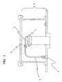
- a container of the antenna device of Fig. 1includes an antenna window 5 and a jacket 6.
- a window material made of a dielectric material, and having a lens-like configuration in cross sectionis fitted into the antenna window 5.
- the jacket 6 of the antenna deviceincludes an RF connector 1, a cable 2, a micro-strip antenna 3, and a cold stage 4. These elements together with the jacket 6 form the antenna device.
- the micro-strip antenna 3is made of a superconducting material.
- a vacuum pumpis attached to the antenna device.
- the interior of the jacket 6 of the antenna deviceis substantially vacuumed, and the micro-strip antenna 3 is heat insulated from the outside while also being cooled by a cold stage 4.
- the distance between the antenna window and the micro-strip antenna 3is set to be a predetermined distance determined by a specific dielectric constant, the thickness and the shape of the lens-like window material fitted into the antenna window 5. (See Patent Document 1.)
- a stratosphere-mesosphere ozone monitoring systemis described.
- AOSAcoustic-optical Spectrometer
- the elements of Fig. 2except the second oscillator 411, the third oscillator 412, the AOS 141, the personal computer 425, and the reference oscillator 424, form a main receiver unit 428.
- the first oscillatorincludes a frequency multiplier 421, a harmonic mixer 423, a phase-locked controller 426, and a Gunn oscillator 422. (see Non-patent Document 1)
- Superconducting microstrip antennasthat are directly coupled and gap-coupled to a microstrip transmission line have been designed and fabricated on lanthanum aluminate substrates using Y-Ba-Cu-O superconducting thin films. Measurements from these antennas, including input impedance, bandwidth, efficiency, and patterns, are presented and compared with published models. The measured results demonstrate that usable antennas can be constructed using either of these architectures, although the antennas suffer from narrow bandwidths. In each case, the HTS antenna shows a substantial improvement over an Identical antenna made with normal metals.
- GB 2 303 491 Adiscloses a mictostrip patch or radiating element which is coupled to a dielectric rod by way of a tapered tubular guide formed integrally with the rod.
- An array of radiating elementsmay be formed on a common substrate, and the dielectric rod antennae may be arranged to direct the energy radiated from these elements to a secondary antenna element such as a lens or a dish.
- WO 01/26183 A1discloses a multi-beam radar sensor comprising at least two emitting-receiving patches in which the patches, assigned polyrods and/or a dielectric lens are configured such that they are asymmetrical.
- This asymmetrical configurationresults in the provision of asymmetrical beam paths for the emitting or receiving beams.
- the mean error magnitude of the angle measurement of the radar sensoris less than that of a symmetrical configuration.
- WO 01/61785 A2discloses an antenna device including a dual polarized quad-ridge antenna horn an electrically conductive conduit with first and second opposite ends along a horn axis. Four electrically conductive ridges are carried on an inner side of the electrically conductive conduit.
- a printed wiring board including a dielectric substrateis connected across the first end of the dual polarized quad-ridge antenna horn and transversely to the horn axis. Furthermore, an electrically conductive pattern is formed on the dielectric substrate and defines feed elements for the dual polarized quad-ridge antenna horn.
- WO 97/17706discloses a cabled conductor comprising a plurality of transposed strands each comprising one or more preferably twisted filaments preferably surrounded or supported by a matrix material and comprising textured anisotripoc superconducting compounds which have crystallographic grain alignment that is substantially unidirectional and independent of the rotational orientation of the strands and filaments in the cabled conductor.
- the cabled conductoris made by forming a plurality of suitable composite strands, forming a cabled intermediate from the strands by transposing them about the longitudinal axis of the conductor at a preselected strand lay pitch, and, texturing the strands in one or more steps including at least one step involving application of a texturing process with a primary component directed orthogonal to the widest longitudinal cross section of the cabled intermediate, at least one such orthogonal texturing step occurring subsequent to said strand transposition step.
- the filament cross section, filament twist pitch, and strand lay pitchare cooperatively selected to provide a filament transposition area which is always at least ten times the preferred direction area of a typical grain of the desired anisotropic superconducting compound.
- the texturing steppreferably includes application of a texturing process with a second primary component in a predetermined direction in the plane on the widest longitudinal cross section of the conductor.
- a temperature as low as several tens of degree Kis required to cool an antenna element to improve antenna performance when the antenna of a superconducting material is used.
- a cooling device using a helium gas as a medium and a vacuum jacket for heat insulating a low-temperature operating element and a circuitare required.
- the ratio of the specific dielectric constant of the dielectric material to the specific dielectric constant of the interior of a vacuum deviceis set to be a predetermined value using a dielectric material in an window section of the vacuum device or the cross-sectional shape of the dielectric material is lens-configured.
- the window sectionthus has a lens effect. If the distance between the antenna window and the antenna element satisfies the relationship of [Equation 1], the directivity gain is improved during the reception of radio transmission and reception.
- a plurality of antenna elementsare operatively driven so that the plurality of antenna elements result in improvements in directivity. If intervals between antenna elements are assured to prevent interference between the antenna elements, a container housing the plurality of antenna elements becomes bulky. If an antenna pattern of the antenna element is made of a superconducting material, a heat-insulation vacuum device and a cooling device for maintaining a low-temperature state are required, leading to a bulky size of the entire antenna device.
- the problems associated with the vacuum device and heat insulationare discussed here.
- the vacuum deviceeffectively blocks heat inflow through heat conduction via a solid object and heat conduction via a gaseous body.
- heat inflow through heat radiation from a vacuum containercannot be prevented.
- the heat radiation from the vacuum containeris proportional to the difference between the absolute temperature of the ambient air to the fourth power and the absolute temperature of the cooled element to the fourth power as described by the Stefan-Boltzmann law of [Equation 2]. If a heat insulation material such as a metal sheet or a polyester film having a metal film is contained in the vacuum container, pass of the received radio wave and the transmission of the radio wave can be adversely affected.
- a typical heat insulation problemmay arise. For example, if a large transparent section such as an antenna window is present in a vacuum container, heat is transferred to the antenna element through heat radiation. This can cause an increase in the load on the cooling device, leading to an increase in power consumption of the cooling device. Power feeding and the cooling device under limited installation conditions present difficulty in cooling. Realizing an antenna device incorporating an antenna element having an antenna pattern made of a superconducting material is disadvantageous in terms of compact design and low power consumption. If the CGC 416 is coupled to the waveguide 415 to guide a radio wave from the dish antenna 408 as in the known example 2, heat radiation received by the waveguide 415 is also transferred to the CGC 416. Load on a device for cooling the CGC 416 can be even more increased.
- a circuit forming a transmitter and a receiversuch as a filter circuit and an amplifier circuit, need to be attached to the antenna device. If these circuits are attached external to the vacuum device required to operate the antenna element in a stable manner, an attempt to incorporate the compact design in the transmitter and receiver may fail.
- an antenna deviceas set out in Claim 1.
- the present inventionalso provides a radio-wave receiver as set out in Claim 9.
- the present inventionalso provides a radio-wave transmitter as set out in Claim 11.
- the antenna devicecools the plane-type antenna element, a surface resistance of a conductor forming the plane-type antenna element is lowered, and the overall gain of the plane-type antenna element is increased.
- the waveguideimparts directivity to the plane-type antenna element, the directivity gain of a radio wave transmitted is increased during transmission, and the directivity gain of a received radio wave is increased during reception.
- a waveguidewhich is tubular.
- the height of the tubular waveguideis larger than the quotient that is obtained by dividing a quarter of the wavelength of a transmitted and received radio wave by ⁇ A
- Arepresents an effective specific dielectric constant between the opening of the waveguide and the antenna pattern formation surface of the plane-type antenna element.
- a length of the opening of the waveguide opened toward the plane-type antenna element along at least one axis directionis longer than the quotient that is obtained by dividing half the wavelength of the radio wave by ⁇ A but equal to or shorter than the quotient that is obtained by dividing the wavelength of the radio wave by ⁇ A.
- An antenna deviceincludes a plurality of plane-type antenna elements, a heat insulation container for blocking heat entering from the outside, the heat insulation container having a radio-wave window allowing a radio wave to pass therethrough, and housing the plurality of plane-type antenna elements, a waveguide housed in the heat insulation container and arranged between the radio-wave window and an antenna pattern formation surface of the plane-type antenna element, and cooling means for cooling the plane-type antenna elements.
- the waveguideis shaped and dimensioned so that the directivity of the plane-type antenna element is enhanced, and the plurality of antenna elements are operatively connected to each other.
- the antenna device of this embodimentcools the plane-type antenna element, a surface resistance of a conductor forming the plane-type antenna element is lowered, and the overall gain of each plane-type antenna element is increased.
- the plane-type antenna elementsare equally enhanced in directivity gain.
- the antenna deviceincludes the plurality of plane-type antenna elements.
- the plurality of plane-type antenna elements operatively connectedfunction as a single hybrid antenna.
- the hybrid antennaprovides improved directivity in comparison of the case in which each of individual plane-type antenna elements operates independently.
- An antenna deviceincludes a plane-type antenna element, a heat insulation container for blocking heat entering from the outside, the heat insulation container having a radio-wave window allowing a radio wave to pass therethrough, and housing the plane-type antenna element, a first waveguide housed in the heat insulation container and arranged between the radio-wave window and an antenna pattern formation surface of the plane-type antenna element, a second waveguide external to the heat insulation container and arranged in a manner such that one opening of the second waveguide is in contact with the radio-wave window, and cooling means for cooling the plane-type antenna element.
- the first waveguide and the second waveguideenhance the directivity of the plane-type antenna element.
- the second waveguidecauses the radio wave to converge, and increases the directivity gain during transmission and reception.
- the radio-wave receiverSince the plane-type antenna element and the receiver circuit within the heat insulation container are cooled, resistances of the plane-type antenna element and a conductor of the receiver circuit are lowered. The radio-wave receiver thus operates at a low power loss. Since the plane-type antenna element and the receiver circuit are housed in the heat insulation container, the radio-wave receiver is miniaturized.
- the radio-wave transmitterSince the plane-type antenna element and the transmission signal processor circuit within the heat insulation container are cooled, resistances of the plane-type antenna element and a conductor of the transmission signal processor circuit are lowered. The radio-wave transmitter thus operates at a low power loss. Since the plane-type antenna element and the transmission signal processor circuit are housed in the heat insulation container, the radio-wave transmitter is miniaturized.
- a high directivity gain antenna deviceis described.
- the antenna device, the radio-wave receiver and the radio-wave transmitteroperate at a low power loss.
- the antenna device, the radio-wave receiver and the radio-wave transmitter, each incorporating the plane-type antenna element made of a plurality of superconducting materialsare miniaturized.
- the antenna device, the radio-wave receiver and the radio-wave transmitter, each incorporating the plane-type antenna element made of a superconducting materialare operable at a low power consumption.
- an antenna element on a substratea shield for electromagnetically shielding the antenna element on the substrate, a waveguide, a cooling device for cooling the antenna element, a vacuum pump (for example, a rotary pump, a turbo molecular pump, or a combination thereof), a container for the antenna element, and a heat insulation material disposed between the container of the antenna element and the antenna element.
- a vacuum pumpfor example, a rotary pump, a turbo molecular pump, or a combination thereof
- a container for the antenna elementa heat insulation material disposed between the container of the antenna element and the antenna element.
- the cooling device of the antenna elementuses a cooling medium, thereby cooling a cold plate within the container of the antenna element. As a result, the cooling device of the antenna element can cool the antenna element via the cold plate, etc.
- the vacuum pumpis used to depressurize the interior of the container of the antenna element via a discharge port.
- the vacuum pumpdepressurizes the container of the antenna element to a substantially vacuum state (to 1.3 Pa (1x10E-2 torr) if the rotary pump alone is used, or to 1.3 10 -3 Pa (1x10E-5) to 1.3 10 -5 Pa (1x10E-7 torr) if the turbo molecular pump is used in combination).
- the container of the antenna elementincludes a radio-wave window, a lid for the container of the antenna element, a housing of the container of the antenna element, an O-ring for sealing the air-tightness of the container, a cable for conducting a signal from the antenna element and the like, an radio-frequency RF connector for coupling the cable to the outside of the container, a discharge pipe connecting to the vacuum pump, and a cold plate forming a portion of the cooling device.
- the interior of the container of the antenna elementis maintained at an air-tight state by the O-ring.
- the interior of the containeris maintained at a vacuum state by the vacuum pump.
- the container of the antenna element in the depressurized statecontrols the heat inflow through heat conduction via a solid object or a gaseous body from the outside to the antenna element, and cooling of the antenna element is easily performed.
- the heat insulation materialis disposed between the container of the antenna element and the antenna element, heat inflow through heat radiation from the container of the antenna element to the antenna element is controlled.
- An antenna pattern of the antenna elementis made of a superconducting material, and a surface resistance of the antenna pattern shows a resistance lower than that of copper (Cu) below the critical temperature.
- the antenna pattern of the antenna elementis formed on the surface of the substrate, and is of a plane-type.
- the antenna patternis not limited to the plane-type.
- the antenna pattern of the antenna elementmay have some degree of thickness, or may have a space structure.
- the space structurerefers to a structure in which a substrate includes a plurality of layers with antenna patterns formed in the respective layers.
- the waveguideis arranged within the container of the antenna element, and disposed between the antenna element and the lid of the container of the antenna element.
- the waveguideis fixed to the container of the antenna element and grounded via the container of the antenna element. There is no thermal contact via a solid body or a gaseous body between the waveguide and the antenna element.
- the height of the waveguidefalls within a range that increases the directivity gain in the emission of the radio wave from the antenna element, and is preferably within a range from the wavelength of the radio wave transmitted from the antenna element to a quarter of the wavelength of the radio wave.
- the antenna elementprovides the following advantages. Since the effect of the waveguide imparts directivity to the radio wave transmitted from the antenna element, the directivity gain of the antenna element is increased.
- the waveguide and the shieldprevent the transmitted radio wave from leaking from the antenna element to the heat insulation material.
- the radio waveis thus transmitted through the radio-wave window with directivity. Since passing of the received radio wave to the antenna element is assured, loss of the radio wave due to the heat insulation material is controlled.
- the cooling devicecan thus be miniaturized.
- Fig. 3is a sectional view of the antenna device.
- the antenna device 35includes a substrate 26, antenna elements 20 on the substrate 26, waveguides 22, a shield 18, a vacuum valve 39, a vacuum pump 30, a container 34 for the antenna element, a cold plate 27, a pipe 31, a cooling medium 32, and a compressor 15.
- the cold plate 27, the pipe 31, and the compressor 15form a cooling device that uses adiabatic expansion of the cooling medium 32, namely, based on the pulse tube principle or the Stirling cycle principle.
- the cooling devicecools the substrate 26 on the cold plate 27, and the antenna elements 20 on the substrate 26.
- the cooling medium 32is typically a helium gas.
- a substance for enhancing heat conductionsuch as a copper metal block, indium or grease for improving adherence.
- the type of the cooling deviceis the one based on the pulse tube principle or the Stirling cycle principle.
- the background exampleis not limited to these.
- a pipeis arranged within the cold plate 27 to circulate one of liquid helium and liquid nitrogen.
- the antenna element container 34includes a radio-wave window 21, a lid 24 for the container of the antenna element, a body 33 of the antenna element container 34, a lid O-ring 23, arranged between the lid 24 of the antenna element container 34 and a junction portion of the body 33, for maintaining air-tightness of the container, a cable 17 conducting signals input from outside the antenna element container 34 and output from the antenna element, a RF connector 16, a discharge port 28 coupled to a vacuum pump 30, and lock screws 25.
- the radio-wave window 21is used to receive a radio wave from outside the antenna element container 34 and transmit a radio wave from the antenna element container 34.
- the RF connector 16is used to connect an external cable to the cable 17 that conducts input and output signals between the antenna element and the outside, and handles high-frequency signals.
- the lock screws 25secure the antenna element container 34 to the lid 24 of the antenna element container 34.
- the interior of the antenna element container 34is sealed by the lid 24 to an airtight state.
- the vacuum pump 30is used to depressurize the interior of the antenna element container 34 via the discharge port 28 connected to the vacuum pump 30 and a vacuum valve 39. More specifically, the vacuum pump 30 depressurizes the interior of the antenna element container 34 to a vacuum state of 1.3Pa (1x10E-2) through 1.3 10 -4 Pa (1x10E-6 torr) hereinafter referred to as quasi-vacuum state).
- the discharge port 28 and the vacuum valve 39are joined to each other using so-called metal shield, maintaining a high degree of airtightness.
- the O-ringsuch as the lid O-ring 23 is set to be metal seal grade, even higher airtightness is assured. If the procedure described below is followed, the above-mentioned quasi-vacuum state is maintained for a long period of time, and even the vacuum pump can be removed.
- Step 1The vacuum pump 30 is used to vacuum the interior of the container of the antenna element to a quasi-vacuum state.
- Step 2Means (not shown) for heating the interior of the antenna element container 34 to a temperature within a range of 70 to 105 °C is attached on one of the lid 24 and the body 33. Baking is performed using the heating means.
- Step 3A getter material (not shown) attached to the antenna element container, typically mounted within the vacuum container, is caused to function with the entire vacuum valve 39 of the antenna element closed.
- the antenna element container 34 in a depressurized statethus prevents heat inflow from the outside to the antenna element.
- the antenna elementis cooled using the above-mentioned cooling device in a manner free from load added thereto.
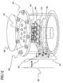
- Fig. 4is a perspective view of a portion of the antenna element container 34 of Fig. 3 , and the interior thereof.
- the antenna element container 34includes eight rectangular antenna elements 20, eight rectangular waveguides 22, each having a rectangular opening opened toward the side of a radio-wave window and an rectangular opening opened toward the side of the antenna element, a shield 18, a cold plate 27, eight cables 17 of the same number as the number of antenna elements (four cables not shown), eight RF connectors 16 (four RF connectors not shown), a lid 24, a radio-wave window 21, a cylindrical antenna element container 34, lock screws 25, and a body 33.
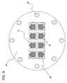
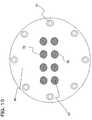
- Fig. 5is a top view of the container of the antenna element, and shows the positional relationship of the lid 24 of the antenna element container, the rectangular radio-wave window 21, the rectangular antenna elements 20, the rectangular openings of the waveguides 22, and the lock screws 25.
- the substrate 26 on which the antenna elements 20 are disposedis arranged on the disk-like cold plate 27.
- the shield 18is arranged on the substrate 26, thereby covering the substrate 26.
- the substrate 26is a substrate made of a dielectric material.
- the substrate 26 "on which the antenna element 20 is disposed"means that an antenna pattern of the substrate 26 is formed on the substrate 26. If the antenna pattern has a strip-line structure, a metal electrode for ground potential is arranged on the backside of the substrate 26.
- the antenna patternmay be of a plane-type or may have a thickness. If the substrate 26 has a multi-layer structure, the antenna pattern may be formed in an intermediate layer.
- the material of the shield 18is a metal such as copper (Cu). The ground potential of the shield 18 is at the same level as the antenna element 20.
- the antenna element 20may have a micro-strip line structure or a coplanar structure, each having an antenna pattern such as a dipole type, a loop type, or a linear antenna type.
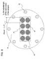
- a set of antenna patternsbecomes rectangular. Eight antenna elements are arranged in a layout of two rows by four columns on the substrate.
- the antenna patternis made of a superconducting material.
- the rectangular-pole-like waveguide 22includes an opening opened toward the side of the antenna element 20 and having a rectangular shape approximately identical in size and shape to the antenna element 20, and an opening opened toward the side of the radio-wave window 21 and having a rectangular shape approximately identical in size and shape to the antenna element 20.
- the waveguide 22is thus arranged between the antenna element 20 and the radio-wave window 21.
- the one opening of the waveguide 22faces the antenna element 20, but is spaced from the antenna element 20 and the shield 18.
- the other opening of the waveguide 22faces the radio-wave window 21 and is connected to the lid 24 at the radio-wave window 21.
- the waveguide 22is in solid-object thermal contact with and electrically connected to the antenna element container 34.
- the waveguide 22is thus grounded via the antenna element container 34.
- a hollow rectangular pole as the waveguide 22is produced from a thin metal sheet having less thermal conductivity, for example, made of stainless steel (SUS304, SUS316 or the like), cupro-nickel, brass, or the like, with the inner surface of the rectangular pole plated with copper (Cu), silver (Ag), or gold (Au).
- a hollow rectangular pole as the waveguide 22is produced from an insulating film with the inner surface thereof coated with a metal film of copper (Cu), silver (Ag), gold (Au), or the like, or with the outer surface thereof coated with a metal film of copper (Cu), silver (Ag), gold (Au), or the like.
- the waveguide 22is shaped and dimensioned so that the directivity of the antenna element 20 is enhanced as described below.
- directivity of the antenna element 20 is enhancedmeans that an emitted radio wave strength or a received radio wave gain is increased at a predetermined direction with reference to directivity intrinsic of the antenna element 20, namely, angular dependency of the intensity of an emitted radio wave, and angular dependency of the intensity of a received radio wave.
- the “increase of the directivity gain” in transmissionrefers to an increase of the ratio of an emitted power of a radio wave emitted in a particular direction to the sum of power of the radio wave emitted in all directions from the antenna element.
- the “increase of the directivity gain” in receptionrefers to an increase of the ratio of a received power of a radio wave received in a particular direction to the sum of power of the radio wave received in all directions to the antenna element.
- the “enhancement of directivity”intensifies power of the transmitted and received radio wave in a particular direction, thereby leading to the "increase of the directivity gain.”
- the height of the waveguide 22preferably falls within a range of about the wavelength of the radio wave transmitted and received by the antenna device of the background example 1 to about a quarter of the wavelength. If the height of the waveguide 22 is too small, no increase is expected in the directivity gain of the transmitted and received radio wave in the vertical direction. If the height of the waveguide 22 is too large, the transmitted and received radio waves traveling through the waveguide 22 are subject to a large loss, and an increase in the directivity gain of the transmitted and received radio waves is limited. However, the height of the waveguide 22 is not limited to about a quarter of the wavelength.
- the length of the rectangular opening of the waveguide 22, facing the antenna element 20, along the long side of the openingpreferably falls within a range from about the wavelength of the transmitted and received radio wave to about half the wavelength of the radio wave.
- the lower limit of the rangeis set to half the wavelength because the length of the long side set to be equal to or less than about half the wavelength causes the transmitted and received radio wave to be cut off.
- the upper limit of the rangeis set to be about the wavelength because the length of the range set to be above the wavelength weakens the convergence of the transmitted and received radio wave and restricts an increase in the directivity gain of the transmitted and received radio wave.
- the transmitted and received radio waveis affected by a specific dielectric constant of the interior of the antenna element container 34 and a specific dielectric constant of the substrate 26.
- the transmitted and received radio waveis affected by a specific dielectric constant of an interior of the waveguide 22.
- the "wavelength" discussed with reference to the background example 1is a wavelength ⁇ 0 / ⁇ Ke of an electromagnetic wave that is a transmitted and received radio wave at each location, where Ke represents an effective specific dielectric constant acting on an electromagnetic field caused by the transmitted and received radio wave and ⁇ 0 represents a wavelength of the transmitted and received radio wave in vacuum (the definition of the wavelength remains unchanged unless otherwise the wavelength is redefined).
- the "effective specific dielectric constant"is determined based on the following teaching.
- the dielectric constantis determined as a proportional coefficient (typically a tensor corresponding to each element of a vector) of the electric flux density (vector) that is proportional to an electric field E (vector representing a direction and a length) in an electromagnetic mode used in space in which the dielectric constant is to be determined.
- the dielectric constantis determined using an electromagnetic field simulator on a computer. More specifically, the dielectric constant is determined generally analyzing specific dielectric constants of a plurality of dielectric materials affecting the space, distance from the dielectric materials, or the shapes of the dielectric materials. The dielectric constant is the one the electromagnetic field resulting from the transmitted and received radio wave responds within the range of the space where the dielectric constant is to be determined.
- the mean(a scalar amount having only a magnitude) of energy of an electric field (vector) is approximately used, and the dielectric constant is represented as simple proportionality constants ⁇ x ⁇ 0 ( ⁇ :specific dielectric constant of a given dielectric material and ⁇ 0 : dielectric constant of the vacuum).
- an electromagnetic waveWhen traveling through a metal-enclosed tubular waveguide, an electromagnetic wave propagates in TE 11 mode as one of basic electromagnetic field modes.
- the electric field at the opening surface of the waveguidehas parallel components only.
- the dielectric constant of the dielectric materialis considered from the parallel component only.
- the ratio of the dielectric constant thus determined to the dielectric constant of the vacuumbecomes a specific dielectric constant.
- the dimension of the waveguidemay be set to be about a quarter of the wavelength.
- the effective specific dielectric constantis determined by accounting for the effect of the waveguide itself at the mounting location of the waveguide.
- the wavelengthis calculated from ⁇ 0 / ⁇ Ke based on the specific dielectric constant, and the dimension of the waveguide is then determined.
- ⁇ 0 / ⁇can be used as a wavelength of the electromagnetic wave ( ⁇ 0 : wavelength in the vacuum, and ⁇ : specific dielectric constant in the waveguide).
- a rectangular window at the radio-wave window 21is carved to a depth equal to half the thickness of the radio-wave window 21 from the outside of the lid 24.
- the rectangular windowencloses of two rows by four columns openings of the waveguides 22.
- a transparent dielectric plate made of quartz, polytetrafluoroethylene, or the like, having a low thermal conductivityis fitted into the rectangular window.
- the plateis glued onto the lid 24 using an adhesive agent or a shield material. Small eight windows of two rows by four columns are arranged from the inside of the container, and receive the waveguides 22.
- the antenna device 35 of the background example 1provides the following advantages. Since the depressurized antenna element container 34 insulates the antenna elements from external heat, the cooling device including the cold plate 27 and the like can maintain the antenna element 20 at a low temperature for a long period of time. Since the surface resistance of the superconducting material forming the antenna elements 20 becomes low at a low temperature equal to or lower than the critical temperature, the gain of the antenna elements 20 is increased.
- the effect of the waveguide 22 between the antenna element 20 and the radio-wave window 21increases the directivity gain of the antenna element 20 during radio wave transmission.
- the waveguide 22guides the radio wave having passed through the radio-wave window 21 of the antenna element container 34 to the antenna element 20 without leakage, the loss of the radio wave through the antenna element container 34 between the antenna element 20 and the radio-wave window 21 is prevented.
- the directivity gain of the antenna element 20is increased.
- the waveguides 22are independently arranged one for each of the antenna elements 20, interference among the antenna elements 20 in the antenna element container 34 is prevented.
- the waveguides 22do not prevent radio waves radiated from the antenna elements 20 from interfering each other outside the antenna element container 34.
- An antenna device 40 of a background example 2is described below with reference to Fig. 6 .
- the antenna device 40is identical in structure to the background example 1 except for a super insulation film 14.
- the super insulation film 14is constructed by laminating a plurality of layers, each layer composed of a ' metal film or a thin insulation polyester film as thick as about 10 ⁇ m with aluminum (A1) deposited thereon and nylon net. The net is arranged between the metal films or the insulation films in order to keep the metal films or the insulation films from being in contact with each other.
- the super insulation film 14thus constructed has the effect of controlling heat inflow through heat radiation from the antenna element container 34 to the antenna element 20.
- the super insulation film 14thus works as a heat insulation material.
- the antenna device 40 of the background example 2thus includes the super insulation film 14 between the antenna element 20 and the wall of the antenna element container 34 within the antenna element container 34, thereby preventing radiation heat from reaching from the antenna element container 34 to the antenna element 20.
- the load on the cooling device including the cold plate 27can be reduced.
- the cooling devicecan thus be miniaturized, and the entire antenna device is also miniaturized.
- the waveguide 22 and the shield 18increase the directivity gain of the radio wave transmitted from the antenna element 20 regardless of the distance between the antenna element 20 and the radio-wave window 21, and the presence of the super insulation film 14.
- the waveguide 22guides the radio wave having passed through the radio-wave window of the antenna element container 34 without leakage involved. Regardless of the distance between the antenna element 20 and the radio-wave window 21, the super insulation film 14 is prevented from blocking radio wave.
- Fig. 7is a perspective view illustrating a portion of the antenna device of the example 3.
- Fig. 8is a top view of the antenna device of the background example 3.
- the elements of the antenna device of the background example 3are different from those of the antenna device of the background example 1 in the following points.
- Figs. 7 and 8show the differences in that the antenna pattern of an antenna element 48 forming the antenna device of the background example 3 is circular, that a small window of the inside surface of an antenna element container 52 of a radio-wave window 45 is circular, and that a waveguide 47 is a cylinder and has a circular opening opened toward the antenna element 48, having almost the same shape and size as the antenna pattern of the antenna element 48, and a circular opening opened toward the radio-wave window 45, having almost the same shape and size as the inner small window of the radio-wave window 45.
- the antenna element 48, the radio-wave window 45, and the waveguide 47have the following advantages in comparison with the corresponding elements in the antenna device of the background example 1.
- the antenna element 48although having the micro-strip structure, is different from the waveguide 22 in that the antenna element 48 has the circular antenna pattern.
- the antenna devicecan receive a circular polarized radio wave that the rectangular antenna pattern is unable to receive.
- the inner small window of the antenna element container 52 in the radio-wave window 45is circular. Since the small window is reduced in area more than when the small window is square, the heat inflow through the radio-wave window 45 is reduced.
- the waveguide 47is the cylinder and has the circular opening opened toward the antenna element 48, having almost the same shape and size as the antenna pattern of the antenna element 48, and the circular opening opened toward the radio-wave window 45, having almost the same shape and size as the inner small window of the radio-wave window 45.
- the wave guide 47has the shape closely fitted into the small window of the radio-wave window 45 and the antenna pattern of the antenna element 48.
- the antenna pattern of the antenna element 48, the waveguide 47, and the small window of the radio-wave window 45are preferably related to each other in shape.
- the diameter of the antenna pattern of the antenna element 48 of the background example 3is preferably about ⁇ /2.
- the "effective wavelength”refers to the wavelength of the transmitted and received radio wave corresponding to the "effective specific dielectric constant" discussed with reference to the background example 1.
- the diameter of the antenna patternis preferably ⁇ 0/ 2/ ⁇ A in view of the antenna element 48 formed on the substrate, where A represents an effective specific dielectric constant taking into consideration the specific dielectric constant of the interior of the antenna element container 52 and the specific dielectric constant of the substrate, and ⁇ 0 represents the wavelength of the transmitted and received radio wave in the vacuum.
- the radio wavehaving the wavelength ⁇ 0 in the vacuum, has a wavelength ⁇ 0 / ⁇ E when it travels in a substance having a specific dielectric constant E.
- the diameter of the opening of the waveguide 47is preferably about ⁇ /2 if the effective wavelength is ⁇ . Since the diameter of the antenna pattern of the antenna element 20 is ⁇ /2, namely, ⁇ 0 /2/ ⁇ A, loss in the radio wave is controlled.
- the small window on the inner surface of the radio-wave window 45is also preferably about ⁇ 0 /2/ ⁇ A.
- the specific dielectric constant of the substrate forming the antenna device of the background example 3may be approximately equal to the specific dielectric constant of the air, and a received radio wave may be 10 GHz.
- the wavelength of the received radio waveis 3 cm if the speed of light in the vacuum.is about 3x10E8 m/s.
- each element of the antenna device of the background example 3is determined based on the above conditions.
- the small window of the radio-wave window 45is about 1.5 cm.
- the radio-wave window 45 containing small windows of two rows by four columnshas a size of 5x9 cm including spacings between the small windows.
- the antenna element container 52 containing the radio-wave window 45is then a cylinder having a circular cross section of a diameter of 15 cm and a height of about 10 cm.
- the height from the bottom surface of the antenna element container 52 to the top surface of the cold plateis about 5 cm. Since the thickness of the antenna element container 52 is about 1 cm, the waveguide 47 is a cylinder having a height of 1 to 3 cm with a bottom section being circular with a diameter of about 1.5 cm.
- the antenna device of the background example 3 with the circular antenna pattern of the antenna element 48can capture a radio wave of a mode, which is difficult to capture with a rectangular antenna pattern.
- the antenna device of the background example 3captures a circular polarized radio wave.
- Fig. 9is a perspective view illustrating a portion of the antenna device of the embodiment 1.
- Fig. 10is a top view of the antenna device of the embodiment 1.
- Fig. 11is a perspective view of a waveguide 62 forming the antenna device of the embodiment 1.
- the elements of the antenna device of the embodiment 1are different from those of the antenna device of the background example 1 in the following points.
- the antenna device of the embodiment 1is different from the antenna device of the background example 1 in that a waveguide 62 forming the antenna device of the embodiment 1 is a cylinder tapered from an antenna element 63 to a radio-wave window 59, that the radio-wave window 59 is a small circular window, and that an antenna pattern of the antenna element 63 having a micro-strip line structure is circular.
- a transparent plate having a specific dielectric constant ⁇ 1is fitted into the radio-wave window 59.
- ⁇ 0represent the wavelength of a radio wave traveling in the vacuum, and the wavelength of the radio wave becomes ⁇ 0 / ⁇ 1 when the radio wave travels through the radio-wave window 59.
- the diameter of the circular radio-wave window 59is preferably ⁇ 0 /2/ ⁇ 1 . If the diameter of the circular radio-wave window 59 is less than ⁇ 0 /2/ ⁇ 1 , passing of the radio wave is blocked according to theory of electromagnetism. If the diameter of the circular radio-wave window 59 is more than ⁇ 0 /2/ ⁇ 1 , heat inflow to the antenna element through heat radiation from the outside increases.
- Fig. 11is a perspective view of a waveguide 62 that is a cylinder tapered from the antenna element 63 to the radio-wave window 59.
- the diameter of an opening 62a of the waveguide 62 opened to the antenna element 63is larger than the diameter of a second opening 62b opened to the radio-wave window 59.
- the waveguide 62is a unitary body having a specific dielectric constant of ⁇ 1 , and a low-resistance metal such as silver (Ag), copper (Cu), gold (Au), or the like is deposited onto the outer circumference of the waveguide 62.
- a low-resistance metalsuch as silver (Ag), copper (Cu), gold (Au), or the like is deposited onto the outer circumference of the waveguide 62.
- the waveguide 62has such a shape is discussed below. Since the specific dielectric constant of the plate fitted into the radio-wave window 59 and the specific dielectric constant of the waveguide 62 are ⁇ 1 , the effective specific dielectric constant of the waveguide 62 in the vicinity of the second opening 62b opened to the radio-wave window 59 is about ⁇ 1 and the wavelength of the radio wave having passed through the radio-wave window 59 is ⁇ 0/2/ ⁇ 1 . The diameter of the small circular window of the radio-wave window 59 is equalized with the diameter of the second opening 62b of the waveguide 62.
- the radio waveis affected by the specific dielectric constant of the interior of an antenna element container 55 in the quasi-vacuum the specific dielectric constant of the substrate having the antenna element 63, and the specific dielectric constant of the waveguide 62.
- ⁇ 2represent an effective specific dielectric constant of the waveguide 62 in the vicinity of the first opening 62a, and the wavelength of the radio wave having passed through the waveguide 62 is expected to be ⁇ 0 /2/ ⁇ 2 .
- the diameter of the first opening 62a of the waveguide 62is preferably ⁇ 0 /2/ ⁇ 2 .
- the waveguide 62is preferably a cylinder with the first circular opening 62a having a diameter of ⁇ 0 /2/ ⁇ 2 and with the second circular opening 62 having a diameter of ⁇ 0 /2/ ⁇ 1 .
- the height of the waveguide 62preferably falls within a range of ⁇ 0 /4/ ⁇ 1 to ⁇ 0 / ⁇ 1 . If the height is too small, the directivity gain is not increased during the radio wave transmission. If the height is too large, the radio wave suffers from loss when the radio wave travels through the waveguide 62.
- the shape of the antenna pattern of the antenna element 63is simply determined chiefly taking into consideration the specific dielectric constant of the antenna element container 55 in the quasi-vacuum state and the specific dielectric constant of the substrate having the antenna element 63.
- ⁇ 3represent an effective specific dielectric constant
- the diameter of the antenna patternhas preferably a circular shape having a diameter of ⁇ 0 /2/ ⁇ 3 .
- the radio waveis affected more by the specific dielectric constant of the interior of the antenna element container 55 than the specific dielectric constant of the waveguide 62 in the vicinity of the antenna pattern of the antenna element 63. Since the specific dielectric constant of the interior of the antenna element container 55 is approximately equal to the specific dielectric constant of the vacuum, ⁇ 3 is expected to be smaller than ⁇ 2 . If the area of the radio-wave window 59 and the area of the antenna pattern of the antenna element thus determined are compared, the area of the radio-wave window 59 is smaller.
- the antenna device of the embodiment 1provides the advantages similar to those of the antenna device of the background example 1. Because of the above difference, the area of the radio-wave window 59 is smaller the area of the antenna element 63. The antenna element 63 exposed to direct radiation heat from the outside via the radio-wave window 59 is thus smaller. The radio-wave window 59 thus shaped prevent the transmitted and received radio wave from diverging between the antenna element 63 and the radio-wave window 59.
- the load on the cooling device including the cold plate 65is reduced.
- the cooling deviceis thus miniaturized and the entire antenna device is accordingly miniaturized.
- the waveguide 62is the cylinder with the circular opening opened toward the radio-wave window 59 smaller and the circular opening opened toward the antenna element 63 larger.
- Fig. 12is a perspective view illustrating a portion of the antenna device of the embodiment 2.
- the antenna device of the embodiment 2is identical in structure to the antenna device of the embodiment 1 except that the antenna device of the embodiment 2 includes an external waveguide 68.
- the antenna device of the embodiment 2includes the waveguide 68 external to the antenna element container 55 in addition to the antenna device of the embodiment 1.
- the external waveguide 68is arranged outside the antenna element container 55, and contains at the bottom thereof all radio-wave windows 59.
- the external waveguide 68is arranged to be in contact with the radio-wave windows 59, and is shaped and dimensioned so that the directivity of the antenna element 63 is enhanced.
- the external waveguide 68is preferably produced by rolling a metal sheet into a cylinder or rolling into a cylinder an insulation film made of polyester with a metal such as silver (Ag), cupper (Cu), gold (Au) or the like deposited thereon.
- the shape of the external waveguide 68is shaped so that the opening thereof in contact with the antenna element container 55 is smaller in area than the other opening.
- the shape of the external waveguide 68is not necessarily the one shown in Fig. 12 .
- the external waveguide 68may be shaped into a cylinder having a circular cross section with uniform diameter. Even the external waveguide 68 having such a shape enhances the directivity of the antenna element 63.
- the height of the external waveguide 68preferably falls within a range from the wavelength of the transmitted and received radio wave to a quarter of the wavelength of the radio wave.
- the antenna device of the embodiment 2increases the directivity gain of the antenna element during transmission, in addition to the advantages of the antenna device of the embodiment 1.
- the radio wave, condensed by the radio-wave window 59,is thus intensified when received at the antenna element 63.
- the antenna device of the background example 4includes the same elements as the antenna device of the background example 1 except that a waveguide 74 is shaped and dimensioned to enhance the directivity of the antenna element 72 and that the distance between the waveguide 74 and the antenna element 72 is less than a quarter of the wavelength ⁇ .
- Fig. 13is a sectional view of the top portion of the container of the antenna element. Referring to Fig. 13 , the antenna element 72 is spaced apart from the waveguide 74 but the distance therebetween is less than a quarter of the wavelength ⁇ .
- the waveguide 74is also spaced apart from a shield 71.
- the distance therebetweenis set to be less than the quarter of the wavelength ⁇ of the transmitted and received radio wave. The reason is described below.
- the received radio waveis confined to within the waveguide 74 from the radio-wave window 73 to the opening of the waveguide 74 opened toward the antenna element 72.
- the received radio wavemay travel freely in space, and stray. If the distance between the waveguide 74 and the antenna element 72 is large, the radio wave may diverge.
- the radio wave transmitted from the antenna element 72may diverge. If the distance between the waveguide 74 and the antenna element 72 is large, the radio wave traveling through the waveguide 74 may weaken, resulting in no increase in directivity gain.
- the waveguide 74is spaced apart from each of the shield 71 and the antenna element 72 in order to block the heat inflow from the waveguide 74 through solid-body heat conduction.
- the radio wave having passed through the radio-wave window 73reaches the antenna element 72 without being diverged even after exiting the waveguide 74 during reception.
- the radio wave transmitted from the antenna element 72travels through the waveguide 74, and the directivity gain of the antenna element 72 is thus increased.
- the antenna device of the background example 4also provides the advantages of the antenna device of the background example 1, namely, compact design is implemented in the cooling device and thus the entire antenna device.
- the receiver 97includes an antenna device identical to the antenna device 35 of the background example 1.
- the antenna device of the receiver 97includes a substrate, antenna elements on the substrate, waveguides, a shield, a discharge O-ring, a vacuum valve, a vacuum pump, a container of the antenna element, a cold plate, a pipe, a cooling medium, and a compressor.
- the positional relationship of the antenna elements, the waveguides, and the radio-wave window in the lid of the container of the antenna elementremains unchanged from that of the antenna device of the background example 1.
- the antenna device of the background example 5is identical to the antenna device of the background example 1 in that the waveguide thereof is shaped and dimensioned for enhancing directivity.
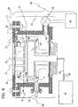
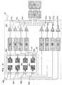
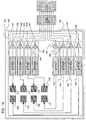
- Fig. 14illustrates a portion of the receiver 97 including the antenna device.
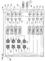
- a plurality of antenna elements 80a-80h in the antenna element containerthere are shown a plurality of antenna elements 80a-80h in the antenna element container, a substrate 81 for the antenna elements in the antenna element container, a plurality of BPFs (band pass filters) 83-90 arranged external to the antenna element container and respectively connected to the antenna elements 80a-80h, low-noise amplifiers 91a-91h respectively connected to the BPFs 83-90 and arranged external to the antenna element container, an IF (interface) 93 external to the antenna element container, and a signal processor circuit 95.
- the receiver 97thus includes the BPFs 83-90, the low-noise amplifiers 91a-91h, each shown in Fig. 13 , and the antenna device identical to the antenna device of the background example 1.
- the BPFs 83-90are filters for extracting signals of particular frequencies from the signals derived from the radio wave received by the antenna elements.
- the BPFs 83-90receives signals from the antenna elements 80a-80h in the container of the antenna element via cables and RF connectors, and outputs the signals of the particular frequencies to the low-noise amplifiers 91a-91h.
- the low-noise amplifiers 91a-91hamplify the signals from the BPFs 83-90, and then output the amplified signals to the IF 93.
- the IF 93accurately conducts the signals, received buy the receiver 97, to a signal processor circuit 95.
- the IF 93also regulates the phases of the signals from the antenna elements 80a-80h.
- the phrase "operatively connecting the antenna elements 80a-80h”is defined as “causing the antenna elements 80a-80h to integrally operate by regulating the phases of the received signals and manipulating a signal from a particular antenna element.”
- the signal processor circuit 95has a function to cause a plurality of antenna elements as a hybrid antenna by operatively connecting the antenna elements.
- the receiver 97 of the background example 5concurrently supplies the received signals from the plurality of antenna elements 80a-80h to the signal processor circuit 95.
- the antenna elements 80a-80hare operatively connected as a hybrid antenna, such as a phased-array antenna or an adaptive array antenna.
- a receiver 153 of a background example 6is described below with reference to Figs. 15 and 16 .
- the antenna device contained in the receiver 153 of the background example 6is identical to the antenna device 35 of the background example 1.
- the antenna device in the receiver 153includes a substrate, antenna elements on the substrate, waveguides, a shield, a discharge O-ring, a vacuum valve, a vacuum pump, a antenna element container, a cold plate, a pipe, a cooling medium, and a compressor.
- the positional relationship of the antenna elements, the waveguide, and the radio-wave window in the lid of the container of the antenna elementremains unchanged from that of the antenna device 35 of the background example 1.
- the antenna device of the background example 6is also identical to the antenna device of the background example 1 in that the waveguide is shaped and dimensioned for enhancing directivity.
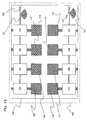
- Fig. 15illustrates a portion of the receiver 153 of the background example 6 containing the antenna device.
- the substrate 149 including the circuit, the patterns, and the elements, and the shield 112are housed in a container of the antenna elements.
- the bias-tee patterns 121 and 120cancel the effect of the feeder patterns 122 and 117 on a radio wave.
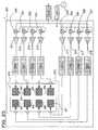
- Fig. 16illustrates the receiver 153 of the background example 6 and a circuit connected thereto.
- Fig. 16is as block diagram of the receiver circuits 100-107 on the substrate 119 of Fig. 15 . More specifically, Fig. 16 illustrates the plurality of antenna elements 108-111 and 113-116 the receiver circuits 100-107 respectively connected to the antenna elements and composed of BPFs 133-140 and low-noise receiver circuit 141-148 respectively connected to the BPFs, all these mounted on the same substrate, and an IF 150 and a signal processor circuit 151 not mounted on the same substrate.
- the antenna device containing the antenna elements 108-115 in an antenna element container 152 and the receiver circuits 100-107form the receiver 153 of the background example 6.
- the IF 150 and the signal processor circuit 151are arranged external to the antenna element container 152 and not included in the receiver 153 of the background example 6. In the same way as described with reference to the background example 5, the IF 150 transfers the signals received by the antenna elements 108-115 to the signal processor circuit 151, and the signal processor circuit 151 processes the received signals.
- the receiver of the background example 6is different from the receiver of the background example 5 in that the antenna elements 108-115 and the receiver circuits 100-107 are arranged in the container of the antenna elements and are cooled together.
- the receiver circuits 100-107 and the antenna deviceare integrated into the receiver 153, thereby miniaturizing the receiver 153. Since the receiver circuits 100-107 are also cooled, performance of the elements of the receiver circuits 100-107 is enhanced. Amplitudes of received signals are increased and filter performance is enhanced.
- a receiver 220 of the background example 7includes an antenna device identical to the antenna device 35 of the background example 1.
- the antenna device of the receiver 220includes a substrate, antenna elements on the substrate, waveguides, a shield, a discharge O-ring, a vacuum valve, a vacuum pump, a container of the antenna element, a cold plate, a pipe, a cooling medium, and a compressor.
- the positional relationship of the antenna elements, the waveguides, and the radio-wave window in the lid of the container of the antenna elementremains unchanged from that of the antenna device 35 of the background example 1.
- the antenna device of the background example 7is also identical to the antenna device 35 of the background example 1 in that the waveguide is shaped and dimensioned for enhancing directivity.
- Fig. 17illustrates a portion of the receiver 220 of the background example 7 containing the antenna device.
- the antenna elements 163-170, the receiver circuits 155-162, the substrate 175, and the shield 176are arranged in the container of the antenna elements, and form the receiver 220 of the background example 7, together with the antenna device containing the container of the antenna elements.
- Each of the antenna elements 163-182has a circular antenna pattern. Power is fed to the antenna elements 163-182 via the feeder points 175-182 from below the substrate.
- the feeder points 175-182are off-centered from the center of the circular antenna patterns of the corresponding antenna elements with one feeder point in one circular antenna pattern in order to make more pronounced the magnitudes of the received signals and difference in phase between the received signals.
- the angle of vibration mode generated in the circular antenna patternbecomes different depending on difference in polarization plane of the circular polarized wave. If the feeder point is off-centered, a time difference to power feeding becomes different depending on the angle of the vibration mode. The difference in the vibration mode results in a difference in phase of the received signals.
- the bias-tee patterns 171 and 173cancel the effect of the feeder patterns 172 and 174 on the radio wave.
- Fig. 18illustrates the substrate 175 of Fig. 17 , the plurality of circular antenna elements 163-170 on the substrate 175, the receiver circuits 155-162 respectively corresponding to antenna elements 210-217, and including BPFs 190-197, and low-noise amplifiers 200-207, and an IF 190 and a signal processor circuit 219, both not mounted on the substrate 175.
- the antenna elements 210-217 and the receiver circuits 190-197are arranged in an antenna element container 218.
- the IF 190 and the signal processor circuit 219are arranged external to the antenna element container 152, and do not form the receiver of the background example 7.
- the IF 190transfers the signals received by the antenna elements 163-170 to the signal processor circuit 219 and the signal processor circuit 219 processes the received signals.
- the IF 190 and the signal processor circuit 219have the same functions as the IF 150 and the signal processor circuit 151 previously discussed with reference to the background example 6.
- the IF 190 and the signal processor circuit 219are different from the IF 150 and the signal processor circuit 151 in the process method of the received signal that is based on a circular polarized wave as a type of handled radio wave.
- the receiver 220is different from the receiver 153 of the background example 6 in that the shape of the antenna pattern of each of the antenna elements 163-170 is circular.
- the receiver 220 of the background example 7provides the same advantages as the receivers of the background example 5 and the background example 6, each incorporating the antenna device of the background example 1. With the circular pattern of the antenna elements, if the plurality of antenna elements are operatively connected, the antenna elements 163-170 functioning as a hybrid antenna work on a circular polarized wave.
- the antenna element made of a superconducting material in accordance with the background example 8is the antenna element used in the antenna devices of the background example 1 through the background example 4, and referred to as a plane-type antenna having an antenna pattern disposed on a substrate. (In the discussion of the background example 8, the plane-type antenna element is simply referred to an "antenna element.")
- the antenna pattern of an antenna element 233 made of a superconducting material in accordance with the background example 8has a size preferably equal to 1/2 ⁇ or 1/4 ⁇ as shown in Fig. 19 where ⁇ represents the wavelength of the radio wave to be received.
- the antenna pattern having a size of 1/2 ⁇ and 1/4 ⁇provides good matching between the received radio wave and the antenna pattern. When the radio wave is received, current canceling within the antenna is controlled.
- Fig. 19illustrates a substrate 231 of an antenna element 233 of the background example 8, an antenna pattern 230 made of a superconducting material and disposed on the substrate, and a ground conductor 232 made of a superconducting material and disposed on the back side of the substrate. Power feeding is performed between two L-shaped patterns forming the antenna pattern 230.
- the antenna pattern 230is a so-called dipole antenna.
- the size of the antenna pattern 230is about half the wavelength.
- the wavelengthhas the same definition as the "wavelength" discussed with reference to the background example 1.
- the antenna element 233may be composed of a single antenna pattern.
- an antenna pattern 235composed of a plurality of T-type linear antenna patterns shown in Fig. 20 may also be acceptable.
- the antenna element of the background example 8may be an antenna pattern 240 of Fig. 21 as a different antenna pattern.
- the antenna pattern 240is composed of a plurality of patch-type antenna patterns connected. ( Fig. 21 is quoted " High-Temperature Superconducting Microwave Circuits" Zhi-Yuan Shen, Artch House Microwave Library P134-145 .)
- the wavelength in the vacuumis about 3 cm.
- the size of the substrate 231 of the antenna element of Fig. 18may be about 2 cm x 2 cm.
- the size of the substrate of Figs. 20 and 21is about 12 cm x 12 cm, for example.
- the superconducting material forming the antenna element of the background example 8may be preferably one of REBCO system (containing a rare earth element, barium (Ba), copper (Cu), and oxygen (O)), a BSCCO system (containing bismuth (Bi), strontium (Sr), calcium (Ca), copper (Cu), and oxygen (O)), and a PBSCCO system (lead (Pb), bismuth (Bi), strontium (Sr), calcium (Ca), copper (Cu), and oxygen (O)).
- REBCO systemcontaining a rare earth element, barium (Ba), copper (Cu), and oxygen (O)
- BSCCO systemcontaining bismuth (Bi), strontium (Sr), calcium (Ca), copper (Cu), and oxygen (O)
- PBSCCO systemlead (Pb), bismuth (Bi), strontium (Sr), calcium (Ca), copper (Cu), and oxygen (O)
- the superconducting materialneeds to be a high-
- the superconducting materialUnder low temperature, the superconducting material provides a low surface resistance, and has tens of milli ohms ( ⁇ ) in a millimeter wave range, and provides advantages as a material of the antenna element over copper (Cu).
- the superconducting materials categorized as the REBCO systemincludes Ym1Bam2Cum3Om4 (0.5 ⁇ m1 ⁇ 1.2, 1.8 ⁇ m2 ⁇ 2.2, 2.5 ⁇ m3 ⁇ 3.5, 6.6 ⁇ m4 ⁇ 7.0), Ndp1Bap2Cup30p4 (0.5 ⁇ p1 ⁇ 1.2, 1.8 ⁇ p2 ⁇ 2.2, 2.5 ⁇ p3 ⁇ 3.5, 6.6 ⁇ p4 ⁇ 7.0), Ndq1Yq2Baq3Cuq4Oq5 (0.0 ⁇ q1 ⁇ 1.2, 0.0 ⁇ q2 ⁇ 1.2, 0.5 ⁇ q1+q2 ⁇ 1.2, 1.8 ⁇ q3 ⁇ 2.2, 2.5 ⁇ q3 ⁇ 3.5, 6.6 ⁇ p4 ⁇ 7.0), Smp1Bap2Cup3Op4 (0.5 ⁇ p1
- Rare earth elements for use as a superconducting materialinclude Lu, Yb, Tm, Er, Dy, Gd, Eu, La, etc., in addition to the above-mentioned Y, Nd, Sm, and Ho. (Reference is made to the book entitled "Superconducting Material", authored by Kouzou OSAMURA, Yoneda Shuppan).
- the above-mentioned superconducting materialssimply work at a temperature as low as liquid nitrogen (about 50 to 70 K). Cooling is easily performed on an antenna element made of the superconducting material to achieve practicable surface resistance.
- An antenna element made of the REBCO systemcan transmit and receive radio wave at a lower loss than an antenna element made of copper (Cu).
- a superconducting film forming the antenna pattern of the antenna element, made of the superconducting material of the background example 8,is preferably constructed of crystal grains having excellent crystal growth performance and a large grain structure (hereinafter referred to as "grains"). Given the same superconducting material, the better the crystal growth and the larger the grain size, the lower the surface resistance of the superconducting film becomes.
- Double logarithm chart of Fig. 22show plots of frequency-dependent surface resistance of typical low-temperature superconducting materials including Nb 3 Sn, REBCO system, BSCCO system, and Y (yttrium)-Ba-Cu-O representing high-temperature superconducting materials of perovskite-like copper oxide of PBSCCO system.
- the X axisrepresents frequency while the Y axis represents surface resistance.
- Blank triangle symbolsrepresent the surface resistance of Nb 3 Sn
- solid circle symbolsrepresent the surface resistance of epitaxially grown Y-123.
- Y-123is a general expression of Y-Ba-Cu-O, and numerals 123 respectively represent composition ratios of Y, Ba, and Cu.
- Blank circle symbolsrepresent the surface resistance of polycrystal Y-123 not epitaxially grown.
- Broken linerepresents the surface resistance of copper (Cu).
- epitaxially grown Y-123 having large grainsshows a lower surface resistance at low-temperature state.
- the superconducting film forming the antenna pattern of the antenna element of the background example 8has large grains of several ⁇ m diameter in a plane of an a -axis and b-axis observable by a microscope.
- the grainsare preferably c-axis oriented in a direction vertical to the substrate on which the superconducting film is formed.
- the crystal axes of the grainsare preferably regulated.
- the a-axis, the b-axis, and the c-axisare the names of the crystal axes.
- the crystal axesare referred to as the a-axis, the b-axis, and the c-axis in order of the length of crystal grating from short to long.
- a superconducting film composed of c-axis oriented grainsis arranged in a direction vertical to the substrate, one of an a-axis plane and a b-axis plane is parallel to the substrate.
- currentsflow in one of the a-axis plane and the b-axis plane, each of which has a relatively stronger superconducting property, rather than in the c-axis direction known for its relatively weak superconducting property.
- the surface resistance of the superconducting filmbecomes low.
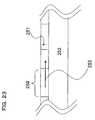
- Fig. 23shows an A-B cross section of the antenna pattern of Fig. 19 .
- a substrate 252having a MgO (100) face as the surface thereof, a superconducting film, a grain 250 of the superconducting film, a direction 251 of the c-axis of the superconducting film, and a direction 253 of the a-axis or b-axis of the superconducting material.
- the grain of the superconducting filmis strongly c-axis oriented in the direction vertical to the MgO (100) face. Because of this, a current from feeder point of the antenna element flows a plane containing one of the a-axis and the b-axis when the antenna element transmits and receives a radio wave.
- the thickness of the film forming the antenna patternpreferably falls within a range of about 100 nm to about 1 ⁇ m in view of the relationship of patterning and magnetic penetration depth.
- the antenna patterns 230, 235, and 240are produced by patterning, on a MgO substrate 252, a superconducting film having large grains and c-axis oriented in the direction vertical to the MgO (100) face as discussed below.
- a substrate having the MgO (100) and a superconducting material composed of the Y-Ba-Cu-O system as a targetare arranged with one surface of the substrate facing to the target in a vacuum container.
- a pulsed laser light beam(for example, KrF laser having a wavelength of 248 nm) is directed to the target.
- the superconducting materialis driven out of the target in a plasma state to be deposited onto the surface of the substrate.
- the interior of the vacuum containeris kept to a depressurized oxygen atmosphere (for example, in an oxygen atmosphere at a depressurized pressure of about 100 mTorr).
- the substrateis heated to about 700 to 800 °C. As a result, a superconducting film is formed on one surface of the substrate.
- the substrate and a target of a superconducting material of the Y-Ba-Cu-O systemare arranged with the other surface of the substrate facing the target within the vacuum container.
- the pulsed laser light beamis directed to the target to drive the superconducting material in a plasma state out of the target to be deposited to the back surface of the substrate.
- the atmosphere in the vacuum container and the state of the substrateremain identical to those used when the superconducting material is deposited onto the one surface of the substrate. As a result, the superconducting film is deposited on the other surface of the substrate.
- the superconducting film formed on the one surface of the substrateis coated with a resist.
- the resistis patterned.
- a wet etching process or a drying etching process such as Ar millingis performed with the patterned resist serving as a mask.
- the superconducting materialis thus patterned.
- the resistis then peeled off.
- the antenna patterns 230, 235, and 240are formed on the one surface of the substrate.
- Electrodesare produced on the antenna pattern, forming the antenna element, on the one surface of the substrate, and on the superconducting film serving as a ground potential on the other surface of the substrate.
- a metal filmmade of gold (Au), silver (Ag), palladium (Pd), titanium (Ti), or the like is formed on both surfaces of the substrate using EB (electron beam) deposition.
- the metal film thus formedis patterned using the photolithographic technique and dry etching technique.
- the electrodesare thus formed on predetermined positions of the antenna elements.
- the superconducting filmhas a large c-axis oriented gain and an adjacent large c-axis oriented grain with one of the a-axis and the b-axis aligned.
- a linear antenna patternis preferably formed along one of the a-axis and the b-axis. This is because the crystal axes of the grains become uniform, thereby resulting in a low surface resistance.
- the vertical segment of the L-shaped patternis preferably aligned with the a-axis direction while the horizontal segment of the L-shaped pattern is aligned with the b-axis direction.
- the rectangular loop-type pattern of Fig. 21the long side of the rectangular pattern is aligned with the a-axis direction while the short side of the rectangular pattern is aligned with the b-axis. The above state is thus achieved.
- the surface resistanceis not only lower than in an ordinary metal.such as copper (Cu), but also lower than in an antenna element in which high-temperature superconducting materials are simply laminated on a substrate. If the antenna element made of the superconducting material of the background example 8 is applied in the background example 1 through background example 4, excellent antenna characteristics are achieved on radio waves having high-frequency components. Since the high-temperature superconducting material does not require a temperature level so low as that of the standard superconducting material, the cooling device can easily cool the antenna element.
- Cucopper
- Fig. 24illustrates a BPF element 258 of a background example 9.
- the BPF element 258 of the background example 9is used in the receiver circuit of the receiver that is used, in each of the background example 6 and the background example 7, together with the antenna device of each of the background example 1 through the background example 4.
- the BPF element 258is mounted on the same substrate as the antenna element of the antenna device of each of the background example 1 through the background example 4.
- the BPF element 258 of the background example 9is mounted on the same substrate as the antenna element, and cooled by the cold plate, the BPF element 258 is preferably made of the same superconducting material as the antenna element of the background example 8. This is because the BPF element 258 is at the same low-temperature state as the antenna element and provides a low surface resistance.
- Fig. 24illustrates a BPF pattern 255 of the BPF element 258 made of the superconducting material, a. substrate 256, and a ground conductor 257.
- the substrate of the BPF elementhas a size of several tens of mm by several tens of mm.
- Four patternsare formed on the substrate, each pattern including two spiral traces.
- the number of patterns, each having two spiral traces,typically falls within a range from several to dozens.
- the number of patternsis usually increased to narrow passband.
- Fig. 24is quoted from Fig. 4 in the specification of the Japanese patent application No. 2002-999997 (filed March 5, 2002, applicant: Fujitsu, Inventors: Manabu KAI, Kazunori YAMANAKA, and others)
- Fig. 2the paper entitled "Development of Superconducting Filter System for IMT-2000", authored by Kai et. al., 2002 Electronics Society Conference, Proceeding SC5-3, the Institute of Electronics,
- the receiver circuitpreferably includes the BPF element 258 made of a superconducting material and an HEMT (High Electron Mobility Transistor) element that operates at low temperature.
- HEMTHigh Electron Mobility Transistor
- the HEMT element with its configuration and structure selectedsuch as PHEMT (Pseudomorphic-HEMT)
- PHEMTPseudomorphic-HEMT
- the BPF element 258can operate at low-noise mode.
- the antenna element, the BPF element 258, and the low-noise amplifierare mounted on the same substrate, and the receiver can thus conduct an amplified signal, namely, a larger signal.
- a signal having a predetermined frequencycan be extracted from a signal received by the antenna element with low loss involved because of a low surface resistance of the BPF element 258.
- the receiver of each of the background example 6 and the background example 7can output a larger signal to the outside.
- a transmitter 305 of a background example 10is described below with reference to Fig. 25 .
- the antenna device contained in the transmitter of the background example 10includes an antenna device identical to the antenna device of the background example 1.
- the antenna device of the transmitter of the background example 10includes a substrate, antenna elements on the substrate, waveguides, a shield, a discharge O-ring, a vacuum valve, a vacuum pump, a container of the antenna elements, a cold plate, a pipe, and a compressor.
- the positional relationship of the antenna elements, the waveguides, and the radio-wave window in the lid of the container of the antenna elementremains unchanged from that of the antenna device of the background example 1.
- the antenna device of the background example 10is also identical to the antenna device of the background example 1 in that the waveguide is shaped and dimensioned for enhancing directivity.
- Fig. 25illustrates a portion of the transmitter 305 containing an antenna device.
- a substrate 270 in a container 303 of antenna elementsthere are shown a substrate 270 in a container 303 of antenna elements, a plurality of antenna elements 260-267 in the antenna element container 303, BPFs 280-287 respectively connected to the antenna elements 260-267 and arranged external to the antenna element container 303, amplifiers 271-278 respectively connected to the BPFs 280-287 and arranged external to the antenna element container 303, mixers 290-297 respectively connected to the amplifiers 271-278, and arranged external to the antenna element container 303, a frequency multiplier 301 connected to the mixers 290-297 and arranged external to the antenna element container 303, an oscillator 301 connected to the frequency multiplier 301 and arranged external to the antenna element container 303, and IF 300 connected to the mixers 290-297 and arranged external to the antenna element container 303.
- the IF 300modulates a signal from an apparatus that represents information into a signal to be transmitted.
- the oscillator 302 and the frequency multiplier 301generate a carrier wave.
- the mixers 290-297mixes the carrier wave and a modulation signal for up conversion, namely, modulates the carrier wave.
- the BPFs 280-287attenuate wanted signals other than a transmission wave, and the amplifiers 271-278 amplify the signal to be transmitted from the antenna.
- the antenna elements of the background example 8are used in the transmitter of the background example 10, a radio wave is transmitted at low loss because the surface resistance of the antenna elements is low.
- the antenna elements 260-267 for transmissionare arranged in the antenna element container 303, and the surface resistance is lowered when the antenna elements 260-267 are cooled.
- the radio waveis thus transmitted at low loss.
- a large amplitude signalis thus transmitted with low power consumed.
- a transmitter 350 of a background example 11is described below.
- An antenna device contained in the background example 11is identical to the antenna device of the background example 1 in that the antenna device includes a container for antenna elements, antenna elements on a substrate, waveguides, a cooling device, and a vacuum pump.
- the positional relationship of the antenna elements, the waveguides, and the radio-wave window in the lid of the container of the antenna elementremains unchanged from that of the antenna device of the background example 1.
- the antenna device of the background example 11is identical to the antenna device of the background example 1 in that the waveguide is shaped and dimensioned for enhancing directivity.
- Fig. 26illustrates a portion of the transmitter 350 containing the antenna device: Referring to Fig. 26 , there are shown a plurality of antenna elements 307a-307h in the antenna element container 347, a substrate 346 for the antenna elements in the antenna element container 347, BPFs 318-325 arranged in the antenna element container 347 and respectively connected to the antenna elements 307a-307h on the substrate 346, amplifiers 310-317 arranged in the antenna element container and respectively connected the BPFs 318-325 on the substrate, mixers 330-337 arranged external to the antenna element container 347 and respectively connected to the amplifiers 310-317, IF 345 arranged external to the antenna element container 347 and connected to the mixers 330-337, a frequency multiplier 341, and an oscillator 341.
- the elements shown in Fig. 26form, together with the antenna device containing the antenna elements 307a-307h in the antenna element container 347, the transmitter 350.
- the IF 345is a circuit for modulating a signal from an apparatus that represents information into a signal to be transmitted.
- the oscillator 340 and the frequency multiplier 341generate a carrier, and the mixers 330-337 mix the carrier and a modulation signal for up conversion, namely, converts the modulation signal to a high-frequency signal.
- the BPFs 318-325attenuate unwanted signals other than a transmission signal, and the amplifiers 310-317 amplify a signal to be transmitted from the antenna.
- the antenna element 233 of the background example 8 and the BPF element 258 of the background example 9can be incorporated into the transmitter 350 of the background example 11.
- radio wavecan be transmitted with low loss involved because the antenna element 233 and the BPF element 258 provide low surface resistances.
- the antenna elements 307a-307h for transmission and the transmitter circuitare arranged in the antenna element container 347 and are cooled.
- the surface resistances of these elementsare lowered, and transmission is performed with low loss involved.
- a large amplitude signalcan be transmitted with low power consumed.
- the transmitter of the background example 11is identical to the transmitter of the background example 10, but performance of both the antenna elements for transmission and the transmitter circuit is increased. The advantages of transmission at low loss and increase in signal amplitude are even more enhanced.
- the transmitter circuitis integrated with the antenna device, the transmitter 350 of the background example 11 can be miniaturized.
- a high directivity gain antenna deviceis provided using an antenna element made of a superconducting material.
- An antenna device, a radio-wave transmitter employing the antenna device, and a radio-wave receiver employing the antenna deviceare operable at low loss.
- the antenna device, the radio-wave receiver, and the radio-wave transmitter, each employing an antenna element made of a plurality of superconducting materialsare miniaturized.
- a cooling system of the antenna device, the radio-wave receiver, and the radio-wave transmitter, each employing an antenna element made of a superconducting materialconsumes low power.
Landscapes
- Waveguide Aerials (AREA)
- Variable-Direction Aerials And Aerial Arrays (AREA)
- Transmitters (AREA)
- Input Circuits Of Receivers And Coupling Of Receivers And Audio Equipment (AREA)
- Superconductor Devices And Manufacturing Methods Thereof (AREA)
- Containers, Films, And Cooling For Superconductive Devices (AREA)
- Details Of Aerials (AREA)
Description
- The present invention relates to an antenna device, a radio-wave receiver, and a radio-wave transmitter, each employing an antenna element made of a superconducting material. Embodiments of the present invention relate to an antenna device, a radio-wave receiver, and a radio-wave transmitter for enhancing directivity gain. Embodiments of the present invention also relate to an antenna device, a radio-wave receiver, and a radio-wave transmitter, each incorporating a miniaturized design. Embodiments of the present invention further relate to an antenna device, a radio-wave receiver, and a radio-wave transmitter, each having a low-power consumption cooling system.
- A demand for high-speed and compact design communication systems is mounting as radio LAN, satellite communications, and IMT-2000 advance. Along with this demand, performance increase and compact design are required of elements forming a communication system, such as antenna, filters, amplifiers, etc. Since the antenna is arranged at the front end of a receiver and a transmitter of a system, an increase in radio-wave transmission efficiency and an increase in radio-wave reception gain of the antenna lead to compact design and substantial improvement in communication characteristics of the entire system.
- The radio-wave transmission efficiency and the radio-wave reception gain need to be increased. To improve general performance, power loss in high-frequency regions in an conductor portion of a high-frequency device containing an antenna element is preferably reduced. To efficiently increase performance, directivity gain is preferably increased.
- The use of a low-resistance superconducting material has been proposed to reduce power loss in high-frequency regions. To realize the idea of using a superconducting material for an antenna device, a heat insulation unit and a cooling unit must be incorporated. The superconducting antenna element needs to be kept at a stabilized cooled state.
- An antenna device as an known example 1 is described with reference to
Fig. 1 . A container of the antenna device ofFig. 1 includes anantenna window 5 and ajacket 6. A window material made of a dielectric material, and having a lens-like configuration in cross section is fitted into theantenna window 5. - The
jacket 6 of the antenna device includes anRF connector 1, acable 2, amicro-strip antenna 3, and a cold stage 4. These elements together with thejacket 6 form the antenna device. Themicro-strip antenna 3 is made of a superconducting material. - A vacuum pump is attached to the antenna device. The interior of the
jacket 6 of the antenna device is substantially vacuumed, and themicro-strip antenna 3 is heat insulated from the outside while also being cooled by a cold stage 4. - The distance between the antenna window and the
micro-strip antenna 3 is set to be a predetermined distance determined by a specific dielectric constant, the thickness and the shape of the lens-like window material fitted into theantenna window 5. (SeePatent Document 1.) - Referring to
Fig. 2 , a stratosphere-mesosphere ozone monitoring system is described. Referring toFig. 2 , there are shown arotatable dish antenna 408, a λ/4plate 409 phase shifting a portion of a radio wave received by thedish antenna 408 by a quarter wavelength, afixed mirror 410 reflecting a radio wave passing through the λ/4 plate, afirst oscillator 427, a heat-insulation dewar 429, awaveguide 415, a CGC (cross guide coupler) 416 coupled to thewaveguide 415, a SIS (superconductor insulator superconductor)mixer 417, an intermediate-frequency amplifier 418, acooling load 419, aradiation shield 420, asecond oscillator 411, athird oscillator 412, an intermediate-frequencysignal processor device 413, an AOS (Acousto-optical Spectrometer) 414, areference oscillator 424, and apersonal computer 425. The elements ofFig. 2 , except thesecond oscillator 411, thethird oscillator 412, the AOS 141, thepersonal computer 425, and thereference oscillator 424, form amain receiver unit 428. The first oscillator includes afrequency multiplier 421, aharmonic mixer 423, a phase-lockedcontroller 426, and aGunn oscillator 422. (see Non-patent Document 1) Patent Document 1
Japanese Unexamined Patent Application Publication No.2003-46325 - Non-patent
Document 1
Hideo Suzuki et. al. IEICE TRANS. ELECTRON., Vol. E79-C, No. 9, Sep., P1219-1227, 1996 - "Superconducting Microstrip Antennas: An Experimental Comparison of Two Feeding Methods" by M.A. Richard et al in IEEE Transactions on Antennas and Propagation, 41(1993) July, No. 7, discloses that the recent discovery of high-temperature superconductors (HTS's) has generated a substantial amount of interest in microstrip antenna applications. However, the high permittivity of substrates compatible with HTS causes difficulty in feeding such antennas because of the high patch edge impedance. In this paper, two methods for feeding HTS microstrip antennas at K and Ka-band are examined. Superconducting microstrip antennas that are directly coupled and gap-coupled to a microstrip transmission line have been designed and fabricated on lanthanum aluminate substrates using Y-Ba-Cu-O superconducting thin films. Measurements from these antennas, including input impedance, bandwidth, efficiency, and patterns, are presented and compared with published models. The measured results demonstrate that usable antennas can be constructed using either of these architectures, although the antennas suffer from narrow bandwidths. In each case, the HTS antenna shows a substantial improvement over an Identical antenna made with normal metals.
GB 2 303 491 A- In "Novel Millimeter ACC Antenna Feed" by D.G. Spencer in: IEE Colloquium on Antennas for Automotives, 10 March 2000, pages 411-419, XP002160302 the construction and performance of a mictostrip-polyrod antenna feed which is discussed and briefly compared to alternative microstrip feeds for dielectric lenses. This novel antenna feed, which was developed for a 77 GHz automotive radar system, enables mictrostrip patch radiators to efficiently illuminate dielectric lenses or reflectors, and may also be applied to microstrip antenna arrays.
WO 01/26183 A1 WO 01/61785 A2 WO 97/17706- A temperature as low as several tens of degree K is required to cool an antenna element to improve antenna performance when the antenna of a superconducting material is used. To achieve such a low temperature, a cooling device using a helium gas as a medium and a vacuum jacket for heat insulating a low-temperature operating element and a circuit are required.
- In the vacuum jacket, major emphasis is placed on a mechanical strength withstanding vacuum encapsulation, and a radio-wave transmissivity with the lowest possible attenuation involved when a received radio-wave reaches an antenna element, and when a radio-wave is transmitted from the antenna element. As a result, a directivity gain of the antenna element becomes less important.
- In the known example 1, the ratio of the specific dielectric constant of the dielectric material to the specific dielectric constant of the interior of a vacuum device is set to be a predetermined value using a dielectric material in an window section of the vacuum device or the cross-sectional shape of the dielectric material is lens-configured. The window section thus has a lens effect. If the distance between the antenna window and the antenna element satisfies the relationship of [Equation 1], the directivity gain is improved during the reception of radio transmission and reception.
- Improvements in the directivity gain of the antenna element are important, and from a different point of view, there is a need for improvement means improving the directivity gain of the antenna element.

- t1: Thickness of the dielectric material fitted into the antenna window
- t2: Distance from the underside of the dielectric material fitted into the antenna window to the antenna element
- ε1: Dielectric constant of the dielectric material fitted into the antenna window
- ε2: Dielectric constant of the space from the underside of the dielectric material fitted into the antenna window to the antenna element
- λ: Wavelength of the radio wave
- In a hybrid antenna, a plurality of antenna elements are operatively driven so that the plurality of antenna elements result in improvements in directivity. If intervals between antenna elements are assured to prevent interference between the antenna elements, a container housing the plurality of antenna elements becomes bulky. If an antenna pattern of the antenna element is made of a superconducting material, a heat-insulation vacuum device and a cooling device for maintaining a low-temperature state are required, leading to a bulky size of the entire antenna device.
- The problems associated with the vacuum device and heat insulation are discussed here. The vacuum device effectively blocks heat inflow through heat conduction via a solid object and heat conduction via a gaseous body. However, heat inflow through heat radiation from a vacuum container cannot be prevented. The heat radiation from the vacuum container is proportional to the difference between the absolute temperature of the ambient air to the fourth power and the absolute temperature of the cooled element to the fourth power as described by the Stefan-Boltzmann law of [Equation 2]. If a heat insulation material such as a metal sheet or a polyester film having a metal film is contained in the vacuum container, pass of the received radio wave and the transmission of the radio wave can be adversely affected.

σ: Stefan-Boltzmann constant (5.669x10E-12 w·cm-2K-4)
κ: Coefficient relating to radiation rate (dependent on material)
q: Heat flux
To: Absolute temperature of the ambient air
Ts: Absolute temperature of the element - A typical heat insulation problem may arise. For example, if a large transparent section such as an antenna window is present in a vacuum container, heat is transferred to the antenna element through heat radiation. This can cause an increase in the load on the cooling device, leading to an increase in power consumption of the cooling device. Power feeding and the cooling device under limited installation conditions present difficulty in cooling. Realizing an antenna device incorporating an antenna element having an antenna pattern made of a superconducting material is disadvantageous in terms of compact design and low power consumption. If the
CGC 416 is coupled to thewaveguide 415 to guide a radio wave from thedish antenna 408 as in the known example 2, heat radiation received by thewaveguide 415 is also transferred to theCGC 416. Load on a device for cooling theCGC 416 can be even more increased. - Even the antenna device is cooled drown into a superconducting state below the critical temperature using a superconducting material for the antenna element, a sufficiently low surface resistance cannot be achieved depending on the selection of a superconducting material and the state of crystallization of a superconducting film forming the antenna element.
- To transmit and receive radio waves, a circuit forming a transmitter and a receiver, such as a filter circuit and an amplifier circuit, need to be attached to the antenna device. If these circuits are attached external to the vacuum device required to operate the antenna element in a stable manner, an attempt to incorporate the compact design in the transmitter and receiver may fail.
- According to the present invention, there is provided an antenna device as set out in
Claim 1. - The present invention also provides a radio-wave receiver as set out in Claim 9.
- The present invention also provides a radio-wave transmitter as set out in Claim 11.
Fig. 1 diagrammatically illustrates an antenna device of a known example 1.Fig. 2 diagrammatically illustrates a stratosphere-mesosphere ozone monitoring system of a known example 2.Fig. 3 diagrammatically illustrates a first background example.Fig. 4 is a perspective view of an antenna element container of the first background example.Fig. 5 is a top view of the antenna element container of the first background example.Fig. 6 diagrammatically illustrates a second background example.Fig. 7 is a perspective view of an antenna element container of a third background example.Fig. 8 is a top view of an antenna element container of the third background example.Fig. 9 is a perspective view of an antenna element container of a first embodiment.Fig. 10 is a top view of the antenna element container of the first embodiment.Fig. 11 is a perspective view of a waveguide of the first embodiment.Fig. 12 is a perspective view of an antenna element container of a second embodiment.Fig. 13 is a sectional view of a fourth background example.Fig. 14 is a block diagram illustrating a receiver of a fifth background example.Fig. 15 diagrammatically illustrates a substrate of a sixth background example.Fig. 16 is a block diagram illustrating a receiver of the sixth background example.Fig. 17 diagrammatically illustrates a substrate of a seventh background example.Fig. 18 is a block diagram of a receiver of the seventh background example.Fig. 19 diagrammatically illustrates antenna elements made of a superconducting material in accordance with an eighth background example.Fig. 20 diagrammatically illustrates linear-type antenna elements of the eighth background example.Fig. 21 diagrammatically illustrates patch-type antenna elements of the eighth background example.Fig. 22 illustrates a frequency-dependent surface resistance of a superconducting material.Fig. 23 is a sectional view of antenna elements of the eighth background example taken along A-B section.Fig. 24 illustrates a pattern of a BPF element of a ninth background example.Fig. 25 is a block diagram of a transmitter of a tenth background example.Fig. 26 is a block diagram of an eleventh background example.- 1
- RF connector
- 2
- Cable
- 3
- Micro-strip antenna
- 4
- Cold stage
- 5
- Antenna window
- 6
- Jacket
- 14
- Super insulation film
- 15
- Compressor
- 16
- RF connector
- 17
- Cable
- 18
- Shield
- 20
- Antenna element
- 21
- Radio-wave window
- 22
- Waveguide
- 23
- Lid O-ring
- 24
- Lid
- 25
- Lock screw
- 26
- Substrate
- 27
- Cold plate
- 28
- Discharge port
- 29
- Discharge port O-ring
- 30
- Vacuum pump
- 31
- Pipe
- 33
- Body
- 34
- Antenna element container
- 35
- Antenna device
- 39
- Vacuum valve
- 40
- Antenna device
- 41
- Body
- 42
- Cable
- 43
- RF connector
- 44
- Lid
- 45
- Radio-wave window
- 46
- Lock screw
- 47
- Waveguide
- 48
- Antenna element
- 49
- Shield
- 50
- Cold plate
- 52
- Antenna element container
- 56
- Body
- 57
- Cable
- 58
- Lid
- 59
- Radio-wave window
- 60
- RF connector
- 61
- Lock screw
- 62
- Waveguide
- 62a
- First opening
- 62b
- Second opening
- 63
- Antenna element
- 64
- Shield
- 65
- Cold plate
- 68
- External waveguide
- 70
- Body
- 71
- Shield
- 72
- Antenna element
- 73
- Radio-wave window
- 74
- Waveguide
- 75
- Lid O-ring
- 76
- Cold plate
- 77
- Lid
- 78
- Substrate
- 79
- Lock screw
- 80a, 80b, 80c, 80d, 80e, 80f, 80g, and 80h
- Antenna elements
- 83, 84, 85, 86, 87, 88, 89, and 90
- BPFs
- 91a, 91b, 91c, 92d, 91e, 91f, 91g and 91h
- Low-noise amplifiers
- 93
- IF
- 95
- Signal processor circuit
- 100, 101, 102, 103, 104, 105, 106, and 107
- Receiver circuits
- 108, 109, 110, and 111
- Antenna elements
- 112
- Shield
- 113, 114, 115, and 116
- Antenna elements
- 117 and 122
- Feeder patterns
- 120 and 121
- Bias tee patterns
- 133, 134, 135, 135, 137, 138, 139, and 140
- BPFs
- 141, 142, 143, 144, 145, 146, 147 and 148
- Low-noise amplifiers
- 149
- Substrate
- 150
- IF
- 151
- Signal processor circuit
- 152
- Antenna element container
- 155, 156, 157, 158, 159, 160, 161 and 162
- Receiver circuits
- 163, 164, 165, 166, 167, 168, 169 and 170
- Antenna elements
- 171 and 173
- Bias tee patterns
- 172 and 174
- Feeder patterns
- 175
- Substrate
- 190, 191, 192, 193, 194, 195, 196 and 197
- BPFs
- 198
- IF
- 200, 201, 202, 203, 204, 205, 206 and 207
- Low-noise amplifiers
- 219
- Signal processor circuit
- 230
- Antenna pattern
- 231
- Substrate
- 232
- Ground conductor
- 233
- Antenna element
- 234
- Feeding
- 235
- Antenna pattern
- 236
- Substrate
- 240
- Antenna pattern
- 241
- Substrate
- 250
- Grain
- 251
- C-axis
- 252
- MgO (100) substrate
- 253
- A-axis or b-axis
- 255
- BPF pattern
- 256
- Substrate
- 257
- Ground conductor
- 258
- BPF element
- 260, 261, 262, 263, 264, 265, 266 and 267
- Antenna elements
- 270
- Substrate
- 271, 272, 273, 274, 275, 276, 277 and 278
- Amplifiers
- 280, 281, 282, 283, 284, 285, 286 and 287
- BPFs
- 290, 291, 292, 293, 294, 295, 296 and 297
- Mixers
- 298
- Antenna element container
- 300
- IF
- 301
- Frequency multiplier
- 302
- Oscillator
- 305
- Transmitter
- 310, 311, 312, 313, 314, 315, 316 and 317
- Amplifiers
- 318, 319, 320, 321, 322, 323, 324 and 325
- BPFs
- 330, 331, 332, 333, 334, 335, 336 and 337
- Mixers
- 340
- Oscillator
- 341
- Frequency multiplier
- 345
- IF
- 346
- Substrate
- 347
- Antenna element container
- 350
- Transmitter
- 407
- 110.836 GHz signal from ozone molecules
- 408
- Dish antenna
- 409
- λ/4 plate
- 410
- Fixed mirror
- 411
- Second oscillator
- 412
- Third oscillator
- 413
- Intermediate frequency signal processor
- 414
- AOS
- 415
- Waveguide
- 416
- CGC
- 417
- SIS mixer
- 418
- Intermediate frequency amplifier
- 419
- Cooling load
- 420
- Radiation shield
- 421
- Frequency multiplier
- 422
- Gunn oscillator
- 423
- Harmonic mixer
- 424
- Reference oscillator
- 425
- Personal computer
- 426
- Phase-locked controller
- 427
- First oscillator
- 428
- Main receiver unit
- Embodiments of the invention are described below. In addition, background examples are described to assist understanding.
- In the following, since the antenna device cools the plane-type antenna element, a surface resistance of a conductor forming the plane-type antenna element is lowered, and the overall gain of the plane-type antenna element is increased.
- Since the waveguide imparts directivity to the plane-type antenna element, the directivity gain of a radio wave transmitted is increased during transmission, and the directivity gain of a received radio wave is increased during reception.
- A waveguide is described which is tubular. The height of the tubular waveguide is larger than the quotient that is obtained by dividing a quarter of the wavelength of a transmitted and received radio wave by √A where A represents an effective specific dielectric constant between the opening of the waveguide and the antenna pattern formation surface of the plane-type antenna element. A length of the opening of the waveguide opened toward the plane-type antenna element along at least one axis direction is longer than the quotient that is obtained by dividing half the wavelength of the radio wave by √A but equal to or shorter than the quotient that is obtained by dividing the wavelength of the radio wave by √A. With the waveguide having the above-described shape and dimensions, the directivity gain of the plane-type antenna element in a vertical direction thereto is easily increased.
- An antenna device is described that includes a plurality of plane-type antenna elements, a heat insulation container for blocking heat entering from the outside, the heat insulation container having a radio-wave window allowing a radio wave to pass therethrough, and housing the plurality of plane-type antenna elements, a waveguide housed in the heat insulation container and arranged between the radio-wave window and an antenna pattern formation surface of the plane-type antenna element, and cooling means for cooling the plane-type antenna elements. The waveguide is shaped and dimensioned so that the directivity of the plane-type antenna element is enhanced, and the plurality of antenna elements are operatively connected to each other.
- Since the antenna device of this embodiment cools the plane-type antenna element, a surface resistance of a conductor forming the plane-type antenna element is lowered, and the overall gain of each plane-type antenna element is increased.
- Since the waveguide imparts directivity to the plane-type antenna element, the plane-type antenna elements are equally enhanced in directivity gain.
- The antenna device includes the plurality of plane-type antenna elements. The plurality of plane-type antenna elements operatively connected function as a single hybrid antenna. As a result, the hybrid antenna provides improved directivity in comparison of the case in which each of individual plane-type antenna elements operates independently.
- An antenna device is described that includes a plane-type antenna element, a heat insulation container for blocking heat entering from the outside, the heat insulation container having a radio-wave window allowing a radio wave to pass therethrough, and housing the plane-type antenna element, a first waveguide housed in the heat insulation container and arranged between the radio-wave window and an antenna pattern formation surface of the plane-type antenna element, a second waveguide external to the heat insulation container and arranged in a manner such that one opening of the second waveguide is in contact with the radio-wave window, and cooling means for cooling the plane-type antenna element. The first waveguide and the second waveguide enhance the directivity of the plane-type antenna element.
- In this antenna device, the second waveguide causes the radio wave to converge, and increases the directivity gain during transmission and reception.
- Since the plane-type antenna element and the receiver circuit within the heat insulation container are cooled, resistances of the plane-type antenna element and a conductor of the receiver circuit are lowered. The radio-wave receiver thus operates at a low power loss. Since the plane-type antenna element and the receiver circuit are housed in the heat insulation container, the radio-wave receiver is miniaturized.
- Since the plane-type antenna element and the transmission signal processor circuit within the heat insulation container are cooled, resistances of the plane-type antenna element and a conductor of the transmission signal processor circuit are lowered. The radio-wave transmitter thus operates at a low power loss. Since the plane-type antenna element and the transmission signal processor circuit are housed in the heat insulation container, the radio-wave transmitter is miniaturized.
- A high directivity gain antenna device is described. The antenna device, the radio-wave receiver and the radio-wave transmitter operate at a low power loss. The antenna device, the radio-wave receiver and the radio-wave transmitter, each incorporating the plane-type antenna element made of a plurality of superconducting materials, are miniaturized. The antenna device, the radio-wave receiver and the radio-wave transmitter, each incorporating the plane-type antenna element made of a superconducting material, are operable at a low power consumption.
- Described below is an antenna element on a substrate, a shield for electromagnetically shielding the antenna element on the substrate, a waveguide, a cooling device for cooling the antenna element, a vacuum pump (for example, a rotary pump, a turbo molecular pump, or a combination thereof), a container for the antenna element, and a heat insulation material disposed between the container of the antenna element and the antenna element.
- The cooling device of the antenna element uses a cooling medium, thereby cooling a cold plate within the container of the antenna element. As a result, the cooling device of the antenna element can cool the antenna element via the cold plate, etc.
- The vacuum pump is used to depressurize the interior of the container of the antenna element via a discharge port. As a result, the vacuum pump depressurizes the container of the antenna element to a substantially vacuum state (to 1.3 Pa (1x10E-2 torr) if the rotary pump alone is used, or to 1.3 10-3 Pa (1x10E-5) to 1.3 10-5 Pa (1x10E-7 torr) if the turbo molecular pump is used in combination).
- The container of the antenna element includes a radio-wave window, a lid for the container of the antenna element, a housing of the container of the antenna element, an O-ring for sealing the air-tightness of the container, a cable for conducting a signal from the antenna element and the like, an radio-frequency RF connector for coupling the cable to the outside of the container, a discharge pipe connecting to the vacuum pump, and a cold plate forming a portion of the cooling device. The interior of the container of the antenna element is maintained at an air-tight state by the O-ring. The interior of the container is maintained at a vacuum state by the vacuum pump. The container of the antenna element in the depressurized state controls the heat inflow through heat conduction via a solid object or a gaseous body from the outside to the antenna element, and cooling of the antenna element is easily performed.
- Since the heat insulation material is disposed between the container of the antenna element and the antenna element, heat inflow through heat radiation from the container of the antenna element to the antenna element is controlled.
- An antenna pattern of the antenna element is made of a superconducting material, and a surface resistance of the antenna pattern shows a resistance lower than that of copper (Cu) below the critical temperature. The antenna pattern of the antenna element is formed on the surface of the substrate, and is of a plane-type. The antenna pattern is not limited to the plane-type. The antenna pattern of the antenna element may have some degree of thickness, or may have a space structure. The space structure refers to a structure in which a substrate includes a plurality of layers with antenna patterns formed in the respective layers.
- The waveguide is arranged within the container of the antenna element, and disposed between the antenna element and the lid of the container of the antenna element. The waveguide is fixed to the container of the antenna element and grounded via the container of the antenna element. There is no thermal contact via a solid body or a gaseous body between the waveguide and the antenna element. The height of the waveguide falls within a range that increases the directivity gain in the emission of the radio wave from the antenna element, and is preferably within a range from the wavelength of the radio wave transmitted from the antenna element to a quarter of the wavelength of the radio wave.
- The antenna element provides the following advantages. Since the effect of the waveguide imparts directivity to the radio wave transmitted from the antenna element, the directivity gain of the antenna element is increased.
- Since the radio wave passing through the radio-wave window of the container of the antenna element is guided by the waveguide to the immediately close position to the antenna element without any leakage, loss of the radio wave in the container of the antenna element is prevented. The directivity gain of the antenna element is increased during reception.
- Even if the heat insulation material is disposed in the container of the antenna element, the waveguide and the shield prevent the transmitted radio wave from leaking from the antenna element to the heat insulation material. The radio wave is thus transmitted through the radio-wave window with directivity. Since passing of the received radio wave to the antenna element is assured, loss of the radio wave due to the heat insulation material is controlled.
- Since the heat insulation material within the container of the antenna element controls heat inflow through heat radiation from the container of the antenna element, no further load is applied on the cooling device of the antenna element. The cooling device can thus be miniaturized.
- An
antenna device 35 of a background example 1 is described with reference toFigs. 3 ,4 , and5 .Fig. 3 is a sectional view of the antenna device. Theantenna device 35 includes asubstrate 26,antenna elements 20 on thesubstrate 26,waveguides 22, ashield 18, avacuum valve 39, avacuum pump 30, acontainer 34 for the antenna element, acold plate 27, apipe 31, a cooling medium 32, and acompressor 15. - From among the above-mentioned elements, the
cold plate 27, thepipe 31, and thecompressor 15 form a cooling device that uses adiabatic expansion of the cooling medium 32, namely, based on the pulse tube principle or the Stirling cycle principle. The cooling device cools thesubstrate 26 on thecold plate 27, and theantenna elements 20 on thesubstrate 26. - The cooling medium 32 is typically a helium gas. Arranged between the
cold plate 27 and thesubstrate 26 is a substance for enhancing heat conduction, such as a copper metal block, indium or grease for improving adherence. - As previously discussed, the type of the cooling device is the one based on the pulse tube principle or the Stirling cycle principle. The background example is not limited to these. For example, a pipe is arranged within the
cold plate 27 to circulate one of liquid helium and liquid nitrogen. - The
antenna element container 34 includes a radio-wave window 21, alid 24 for the container of the antenna element, abody 33 of theantenna element container 34, a lid O-ring 23, arranged between thelid 24 of theantenna element container 34 and a junction portion of thebody 33, for maintaining air-tightness of the container, acable 17 conducting signals input from outside theantenna element container 34 and output from the antenna element, aRF connector 16, adischarge port 28 coupled to avacuum pump 30, and lock screws 25. - The radio-
wave window 21 is used to receive a radio wave from outside theantenna element container 34 and transmit a radio wave from theantenna element container 34. - The
RF connector 16 is used to connect an external cable to thecable 17 that conducts input and output signals between the antenna element and the outside, and handles high-frequency signals. - The lock screws 25 secure the
antenna element container 34 to thelid 24 of theantenna element container 34. - The interior of the
antenna element container 34 is sealed by thelid 24 to an airtight state. - The
vacuum pump 30 is used to depressurize the interior of theantenna element container 34 via thedischarge port 28 connected to thevacuum pump 30 and avacuum valve 39. More specifically, thevacuum pump 30 depressurizes the interior of theantenna element container 34 to a vacuum state of 1.3Pa (1x10E-2) through 1.3 10-4 Pa (1x10E-6 torr) hereinafter referred to as quasi-vacuum state). Thedischarge port 28 and thevacuum valve 39 are joined to each other using so-called metal shield, maintaining a high degree of airtightness. - If the O-ring such as the lid O-
ring 23 is set to be metal seal grade, even higher airtightness is assured. If the procedure described below is followed, the above-mentioned quasi-vacuum state is maintained for a long period of time, and even the vacuum pump can be removed. - Step 1: The
vacuum pump 30 is used to vacuum the interior of the container of the antenna element to a quasi-vacuum state. - Step 2: Means (not shown) for heating the interior of the
antenna element container 34 to a temperature within a range of 70 to 105 °C is attached on one of thelid 24 and thebody 33. Baking is performed using the heating means. - Step 3: A getter material (not shown) attached to the antenna element container, typically mounted within the vacuum container, is caused to function with the
entire vacuum valve 39 of the antenna element closed. - In the
antenna device 35 ofFig. 3 thus constructed, theantenna element container 34 in a depressurized state thus prevents heat inflow from the outside to the antenna element. The antenna element is cooled using the above-mentioned cooling device in a manner free from load added thereto. - The
antenna device 35 of the background example 1 is described below in detail with reference toFigs. 4 and5 .Fig. 4 is a perspective view of a portion of theantenna element container 34 ofFig. 3 , and the interior thereof. Theantenna element container 34 includes eightrectangular antenna elements 20, eightrectangular waveguides 22, each having a rectangular opening opened toward the side of a radio-wave window and an rectangular opening opened toward the side of the antenna element, ashield 18, acold plate 27, eightcables 17 of the same number as the number of antenna elements (four cables not shown), eight RF connectors 16 (four RF connectors not shown), alid 24, a radio-wave window 21, a cylindricalantenna element container 34, lock screws 25, and abody 33. Fig. 5 is a top view of the container of the antenna element, and shows the positional relationship of thelid 24 of the antenna element container, the rectangular radio-wave window 21, therectangular antenna elements 20, the rectangular openings of thewaveguides 22, and the lock screws 25.- Referring to
Fig. 4 , thesubstrate 26 on which theantenna elements 20 are disposed is arranged on the disk-likecold plate 27. Theshield 18 is arranged on thesubstrate 26, thereby covering thesubstrate 26. - The
substrate 26 is a substrate made of a dielectric material. Thesubstrate 26 "on which theantenna element 20 is disposed" means that an antenna pattern of thesubstrate 26 is formed on thesubstrate 26. If the antenna pattern has a strip-line structure, a metal electrode for ground potential is arranged on the backside of thesubstrate 26. The antenna pattern may be of a plane-type or may have a thickness. If thesubstrate 26 has a multi-layer structure, the antenna pattern may be formed in an intermediate layer. To electromagnetically shield the antenna element, the material of theshield 18 is a metal such as copper (Cu). The ground potential of theshield 18 is at the same level as theantenna element 20. - The
antenna element 20 may have a micro-strip line structure or a coplanar structure, each having an antenna pattern such as a dipole type, a loop type, or a linear antenna type. A set of antenna patterns becomes rectangular. Eight antenna elements are arranged in a layout of two rows by four columns on the substrate. The antenna pattern is made of a superconducting material. - The rectangular-pole-
like waveguide 22 includes an opening opened toward the side of theantenna element 20 and having a rectangular shape approximately identical in size and shape to theantenna element 20, and an opening opened toward the side of the radio-wave window 21 and having a rectangular shape approximately identical in size and shape to theantenna element 20. Thewaveguide 22 is thus arranged between theantenna element 20 and the radio-wave window 21. The one opening of thewaveguide 22 faces theantenna element 20, but is spaced from theantenna element 20 and theshield 18. The other opening of thewaveguide 22 faces the radio-wave window 21 and is connected to thelid 24 at the radio-wave window 21. In other words, thewaveguide 22 is in solid-object thermal contact with and electrically connected to theantenna element container 34. Thewaveguide 22 is thus grounded via theantenna element container 34. However, there is neither heat conduction via a solid body between thewaveguide 22 and each of the antenna element and theshield 18 nor heat conduction via a gaseous body between thewaveguide 22 and each of the antenna element and theshield 18. - A hollow rectangular pole as the
waveguide 22 is produced from a thin metal sheet having less thermal conductivity, for example, made of stainless steel (SUS304, SUS316 or the like), cupro-nickel, brass, or the like, with the inner surface of the rectangular pole plated with copper (Cu), silver (Ag), or gold (Au). Alternatively, a hollow rectangular pole as thewaveguide 22 is produced from an insulating film with the inner surface thereof coated with a metal film of copper (Cu), silver (Ag), gold (Au), or the like, or with the outer surface thereof coated with a metal film of copper (Cu), silver (Ag), gold (Au), or the like. - The
waveguide 22 is shaped and dimensioned so that the directivity of theantenna element 20 is enhanced as described below. The statement "directivity of theantenna element 20 is enhanced" means that an emitted radio wave strength or a received radio wave gain is increased at a predetermined direction with reference to directivity intrinsic of theantenna element 20, namely, angular dependency of the intensity of an emitted radio wave, and angular dependency of the intensity of a received radio wave. - The "increase of the directivity gain" in transmission refers to an increase of the ratio of an emitted power of a radio wave emitted in a particular direction to the sum of power of the radio wave emitted in all directions from the antenna element. The "increase of the directivity gain" in reception refers to an increase of the ratio of a received power of a radio wave received in a particular direction to the sum of power of the radio wave received in all directions to the antenna element. The "enhancement of directivity" intensifies power of the transmitted and received radio wave in a particular direction, thereby leading to the "increase of the directivity gain."
- More specifically, the height of the
waveguide 22 preferably falls within a range of about the wavelength of the radio wave transmitted and received by the antenna device of the background example 1 to about a quarter of the wavelength. If the height of thewaveguide 22 is too small, no increase is expected in the directivity gain of the transmitted and received radio wave in the vertical direction. If the height of thewaveguide 22 is too large, the transmitted and received radio waves traveling through thewaveguide 22 are subject to a large loss, and an increase in the directivity gain of the transmitted and received radio waves is limited. However, the height of thewaveguide 22 is not limited to about a quarter of the wavelength. - The length of the rectangular opening of the
waveguide 22, facing theantenna element 20, along the long side of the opening, preferably falls within a range from about the wavelength of the transmitted and received radio wave to about half the wavelength of the radio wave. The lower limit of the range is set to half the wavelength because the length of the long side set to be equal to or less than about half the wavelength causes the transmitted and received radio wave to be cut off. The upper limit of the range is set to be about the wavelength because the length of the range set to be above the wavelength weakens the convergence of the transmitted and received radio wave and restricts an increase in the directivity gain of the transmitted and received radio wave. - In the vicinity of the surface of the
substrate 26 having the antenna pattern of the antenna element, the transmitted and received radio wave is affected by a specific dielectric constant of the interior of theantenna element container 34 and a specific dielectric constant of thesubstrate 26. When traveling through thewaveguide 22, the transmitted and received radio wave is affected by a specific dielectric constant of an interior of thewaveguide 22. The "wavelength" discussed with reference to the background example 1 is a wavelength λ0/√Ke of an electromagnetic wave that is a transmitted and received radio wave at each location, where Ke represents an effective specific dielectric constant acting on an electromagnetic field caused by the transmitted and received radio wave and λ0 represents a wavelength of the transmitted and received radio wave in vacuum (the definition of the wavelength remains unchanged unless otherwise the wavelength is redefined). - The "effective specific dielectric constant" is determined based on the following teaching. The dielectric constant is determined as a proportional coefficient (typically a tensor corresponding to each element of a vector) of the electric flux density (vector) that is proportional to an electric field E (vector representing a direction and a length) in an electromagnetic mode used in space in which the dielectric constant is to be determined.
- Typically, within a range affecting a space containing the space where the dielectric constant is to be determined, emitted electromagnetic field distribution within the range is directly numerically approximated, and then the dielectric constant is determined using an electromagnetic field simulator on a computer. More specifically, the dielectric constant is determined generally analyzing specific dielectric constants of a plurality of dielectric materials affecting the space, distance from the dielectric materials, or the shapes of the dielectric materials. The dielectric constant is the one the electromagnetic field resulting from the transmitted and received radio wave responds within the range of the space where the dielectric constant is to be determined.
- In the case of a simple isotropic dielectric material, the mean (a scalar amount having only a magnitude) of energy of an electric field (vector) is approximately used, and the dielectric constant is represented as simple proportionality constants εxε0 (ε:specific dielectric constant of a given dielectric material and ε0: dielectric constant of the vacuum).
- When traveling through a metal-enclosed tubular waveguide, an electromagnetic wave propagates in TE11 mode as one of basic electromagnetic field modes. The electric field at the opening surface of the waveguide has parallel components only. The dielectric constant of the dielectric material is considered from the parallel component only. The ratio of the dielectric constant thus determined to the dielectric constant of the vacuum becomes a specific dielectric constant.
- More specifically, the dimension of the waveguide may be set to be about a quarter of the wavelength. The effective specific dielectric constant is determined by accounting for the effect of the waveguide itself at the mounting location of the waveguide. The wavelength is calculated from λ0/√Ke based on the specific dielectric constant, and the dimension of the waveguide is then determined. To easily learn the size of the metal-enclosed waveguide made of a uniform material, λ0/√ε can be used as a wavelength of the electromagnetic wave (λ0: wavelength in the vacuum, and ε: specific dielectric constant in the waveguide).
- Referring to the sectional view of
Fig. 3 and the perspective view ofFig. 4 , a rectangular window at the radio-wave window 21 is carved to a depth equal to half the thickness of the radio-wave window 21 from the outside of thelid 24. The rectangular window encloses of two rows by four columns openings of thewaveguides 22. A transparent dielectric plate made of quartz, polytetrafluoroethylene, or the like, having a low thermal conductivity is fitted into the rectangular window. To maintain the quasi vacuum state, the plate is glued onto thelid 24 using an adhesive agent or a shield material. Small eight windows of two rows by four columns are arranged from the inside of the container, and receive thewaveguides 22. - The
antenna device 35 of the background example 1 provides the following advantages. Since the depressurizedantenna element container 34 insulates the antenna elements from external heat, the cooling device including thecold plate 27 and the like can maintain theantenna element 20 at a low temperature for a long period of time. Since the surface resistance of the superconducting material forming theantenna elements 20 becomes low at a low temperature equal to or lower than the critical temperature, the gain of theantenna elements 20 is increased. - The effect of the
waveguide 22 between theantenna element 20 and the radio-wave window 21 increases the directivity gain of theantenna element 20 during radio wave transmission. - Since the
waveguide 22 guides the radio wave having passed through the radio-wave window 21 of theantenna element container 34 to theantenna element 20 without leakage, the loss of the radio wave through theantenna element container 34 between theantenna element 20 and the radio-wave window 21 is prevented. During reception of the radio wave, the directivity gain of theantenna element 20 is increased. - Since the
waveguides 22 are independently arranged one for each of theantenna elements 20, interference among theantenna elements 20 in theantenna element container 34 is prevented. Thewaveguides 22 do not prevent radio waves radiated from theantenna elements 20 from interfering each other outside theantenna element container 34. - Since there is no contact between the
waveguide 22 and theantenna element 20, heat inflow from thewaveguide 22 to theantenna element 20 through solid-body heat conduction is prevented. The load on the cooling means, such as thecold plate 27, cooling theantenna element 20, is reduced, permitting the cooling device and thus the entire antenna device to be miniaturized. - An
antenna device 40 of a background example 2 is described below with reference toFig. 6 . Theantenna device 40 is identical in structure to the background example 1 except for asuper insulation film 14. - The
super insulation film 14 is constructed by laminating a plurality of layers, each layer composed of a ' metal film or a thin insulation polyester film as thick as about 10 µm with aluminum (A1) deposited thereon and nylon net. The net is arranged between the metal films or the insulation films in order to keep the metal films or the insulation films from being in contact with each other. Thesuper insulation film 14 thus constructed has the effect of controlling heat inflow through heat radiation from theantenna element container 34 to theantenna element 20. Thesuper insulation film 14 thus works as a heat insulation material. - The
antenna device 40 of the background example 2 thus includes thesuper insulation film 14 between theantenna element 20 and the wall of theantenna element container 34 within theantenna element container 34, thereby preventing radiation heat from reaching from theantenna element container 34 to theantenna element 20. - With the
super insulation film 14 blocking the radiation heat, the load on the cooling device including thecold plate 27 can be reduced. The cooling device can thus be miniaturized, and the entire antenna device is also miniaturized. - The
waveguide 22 and theshield 18 increase the directivity gain of the radio wave transmitted from theantenna element 20 regardless of the distance between theantenna element 20 and the radio-wave window 21, and the presence of thesuper insulation film 14. - The
waveguide 22 guides the radio wave having passed through the radio-wave window of theantenna element container 34 without leakage involved. Regardless of the distance between theantenna element 20 and the radio-wave window 21, thesuper insulation film 14 is prevented from blocking radio wave. - Background example 3 is described with reference to
Figs. 7 and8 .Fig. 7 is a perspective view illustrating a portion of the antenna device of the example 3.Fig. 8 is a top view of the antenna device of the background example 3. The elements of the antenna device of the background example 3 are different from those of the antenna device of the background example 1 in the following points. Figs. 7 and8 show the differences in that the antenna pattern of anantenna element 48 forming the antenna device of the background example 3 is circular, that a small window of the inside surface of anantenna element container 52 of a radio-wave window 45 is circular, and that awaveguide 47 is a cylinder and has a circular opening opened toward theantenna element 48, having almost the same shape and size as the antenna pattern of theantenna element 48, and a circular opening opened toward the radio-wave window 45, having almost the same shape and size as the inner small window of the radio-wave window 45.- The
antenna element 48, the radio-wave window 45, and thewaveguide 47 have the following advantages in comparison with the corresponding elements in the antenna device of the background example 1. - The
antenna element 48, although having the micro-strip structure, is different from thewaveguide 22 in that theantenna element 48 has the circular antenna pattern. By placing the feeder point to the antenna pattern at a proper location, the antenna device can receive a circular polarized radio wave that the rectangular antenna pattern is unable to receive. - In another difference, the inner small window of the
antenna element container 52 in the radio-wave window 45 is circular. Since the small window is reduced in area more than when the small window is square, the heat inflow through the radio-wave window 45 is reduced. - In yet another difference, the
waveguide 47 is the cylinder and has the circular opening opened toward theantenna element 48, having almost the same shape and size as the antenna pattern of theantenna element 48, and the circular opening opened toward the radio-wave window 45, having almost the same shape and size as the inner small window of the radio-wave window 45. Thewave guide 47 has the shape closely fitted into the small window of the radio-wave window 45 and the antenna pattern of theantenna element 48. - As described below, the antenna pattern of the
antenna element 48, thewaveguide 47, and the small window of the radio-wave window 45 are preferably related to each other in shape. - If the effective wavelength of the transmitted and received radio wave is λ, mutual current canceling is removed within the antenna pattern and the transmitted and received signal rises to a higher level. The diameter of the antenna pattern of the
antenna element 48 of the background example 3 is preferably about λ/2. - The "effective wavelength" refers to the wavelength of the transmitted and received radio wave corresponding to the "effective specific dielectric constant" discussed with reference to the background example 1.
- The diameter of the antenna pattern is preferably
λ 0/2/√A in view of theantenna element 48 formed on the substrate, where A represents an effective specific dielectric constant taking into consideration the specific dielectric constant of the interior of theantenna element container 52 and the specific dielectric constant of the substrate, and λ0 represents the wavelength of the transmitted and received radio wave in the vacuum. The radio wave, having the wavelength λ0 in the vacuum, has a wavelength λ0/√E when it travels in a substance having a specific dielectric constant E. - The diameter of the opening of the
waveguide 47 is preferably about λ/2 if the effective wavelength is λ. Since the diameter of the antenna pattern of theantenna element 20 is λ/2, namely, λ0/2/√A, loss in the radio wave is controlled. - Since the opening of the
waveguide 47 is λ0/2/√A, the small window on the inner surface of the radio-wave window 45 is also preferably about λ0/2/√A. - The specific dielectric constant of the substrate forming the antenna device of the background example 3 may be approximately equal to the specific dielectric constant of the air, and a received radio wave may be 10 GHz. The wavelength of the received radio wave is 3 cm if the speed of light in the vacuum.is about 3x10E8 m/s.
- The size of each element of the antenna device of the background example 3 is determined based on the above conditions. For example, the small window of the radio-
wave window 45 is about 1.5 cm. The radio-wave window 45 containing small windows of two rows by four columns has a size of 5x9 cm including spacings between the small windows. Theantenna element container 52 containing the radio-wave window 45 is then a cylinder having a circular cross section of a diameter of 15 cm and a height of about 10 cm. - The height from the bottom surface of the
antenna element container 52 to the top surface of the cold plate is about 5 cm. Since the thickness of theantenna element container 52 is about 1 cm, thewaveguide 47 is a cylinder having a height of 1 to 3 cm with a bottom section being circular with a diameter of about 1.5 cm. - In addition to the advantages of the antenna device of the background example 1, the antenna device of the background example 3 with the circular antenna pattern of the
antenna element 48 can capture a radio wave of a mode, which is difficult to capture with a rectangular antenna pattern. For example, the antenna device of the background example 3 captures a circular polarized radio wave. - An antenna device of an
embodiment 1 is described below with reference toFigs. 9 ,10 and11 .Fig. 9 is a perspective view illustrating a portion of the antenna device of theembodiment 1.Fig. 10 is a top view of the antenna device of theembodiment 1.Fig. 11 is a perspective view of awaveguide 62 forming the antenna device of theembodiment 1. - The elements of the antenna device of the
embodiment 1 are different from those of the antenna device of the background example 1 in the following points. - As shown in
Figs. 9 and10 the antenna device of theembodiment 1 is different from the antenna device of the background example 1 in that awaveguide 62 forming the antenna device of theembodiment 1 is a cylinder tapered from anantenna element 63 to a radio-wave window 59, that the radio-wave window 59 is a small circular window, and that an antenna pattern of theantenna element 63 having a micro-strip line structure is circular. - A transparent plate having a specific dielectric constant ε1 is fitted into the radio-
wave window 59. - Let λ0 represent the wavelength of a radio wave traveling in the vacuum, and the wavelength of the radio wave becomes λ0/√ε1 when the radio wave travels through the radio-
wave window 59. The diameter of the circular radio-wave window 59 is preferably λ0/2/√ε1. If the diameter of the circular radio-wave window 59 is less than λ0/2/√ε1, passing of the radio wave is blocked according to theory of electromagnetism. If the diameter of the circular radio-wave window 59 is more than λ0/2/√ε1, heat inflow to the antenna element through heat radiation from the outside increases. Fig. 11 is a perspective view of awaveguide 62 that is a cylinder tapered from theantenna element 63 to the radio-wave window 59. The diameter of anopening 62a of thewaveguide 62 opened to theantenna element 63 is larger than the diameter of asecond opening 62b opened to the radio-wave window 59.- The
waveguide 62 is a unitary body having a specific dielectric constant of ε1, and a low-resistance metal such as silver (Ag), copper (Cu), gold (Au), or the like is deposited onto the outer circumference of thewaveguide 62. - The reason why the
waveguide 62 has such a shape is discussed below. Since the specific dielectric constant of the plate fitted into the radio-wave window 59 and the specific dielectric constant of thewaveguide 62 are ε1, the effective specific dielectric constant of thewaveguide 62 in the vicinity of thesecond opening 62b opened to the radio-wave window 59 is about ε1 and the wavelength of the radio wave having passed through the radio-wave window 59 is λ0/2/√δ1. The diameter of the small circular window of the radio-wave window 59 is equalized with the diameter of thesecond opening 62b of thewaveguide 62. - In the vicinity of the
first opening 62a, the radio wave is affected by the specific dielectric constant of the interior of anantenna element container 55 in the quasi-vacuum the specific dielectric constant of the substrate having theantenna element 63, and the specific dielectric constant of thewaveguide 62. Let ε2 represent an effective specific dielectric constant of thewaveguide 62 in the vicinity of thefirst opening 62a, and the wavelength of the radio wave having passed through thewaveguide 62 is expected to be λ0/2/√ε2. The diameter of thefirst opening 62a of thewaveguide 62 is preferably λ0/2/√ε2. - Each of the specific dielectric constant of the interior of the
antenna element container 55 and the specific dielectric constant of the substrate is smaller than the specific dielectric constant of thewaveguide 62, and ε2 is normally smaller than ε1. Referring toFig. 11 , thewaveguide 62 is preferably a cylinder with the firstcircular opening 62a having a diameter of λ0/2/√ε2 and with the secondcircular opening 62 having a diameter of λ0/2/√ε1. - To increase the directivity gain during the transmission of the radio wave from the
antenna element 63, the height of thewaveguide 62 preferably falls within a range of λ0/4/√ε1 to λ0/√ε1. If the height is too small, the directivity gain is not increased during the radio wave transmission. If the height is too large, the radio wave suffers from loss when the radio wave travels through thewaveguide 62. - The shape of the antenna pattern of the
antenna element 63 is simply determined chiefly taking into consideration the specific dielectric constant of theantenna element container 55 in the quasi-vacuum state and the specific dielectric constant of the substrate having theantenna element 63. Let ε3 represent an effective specific dielectric constant, the diameter of the antenna pattern has preferably a circular shape having a diameter of λ0/2/√ε3. With the antenna pattern as large as half the wavelength of the radio wave in the vicinity of the antenna pattern, gain is increased in the radio wave transmission and reception. - The radio wave is affected more by the specific dielectric constant of the interior of the
antenna element container 55 than the specific dielectric constant of thewaveguide 62 in the vicinity of the antenna pattern of theantenna element 63. Since the specific dielectric constant of the interior of theantenna element container 55 is approximately equal to the specific dielectric constant of the vacuum, ε3 is expected to be smaller than ε2. If the area of the radio-wave window 59 and the area of the antenna pattern of the antenna element thus determined are compared, the area of the radio-wave window 59 is smaller. - The antenna device of the
embodiment 1 provides the advantages similar to those of the antenna device of the background example 1. Because of the above difference, the area of the radio-wave window 59 is smaller the area of theantenna element 63. Theantenna element 63 exposed to direct radiation heat from the outside via the radio-wave window 59 is thus smaller. The radio-wave window 59 thus shaped prevent the transmitted and received radio wave from diverging between theantenna element 63 and the radio-wave window 59. - As a result, the load on the cooling device including the
cold plate 65 is reduced. The cooling device is thus miniaturized and the entire antenna device is accordingly miniaturized. - In the
embodiment 1, thewaveguide 62 is the cylinder with the circular opening opened toward the radio-wave window 59 smaller and the circular opening opened toward theantenna element 63 larger. Embodiment 2 is described below with reference toFig. 12. Fig. 12 is a perspective view illustrating a portion of the antenna device of theembodiment 2. The antenna device of theembodiment 2 is identical in structure to the antenna device of theembodiment 1 except that the antenna device of theembodiment 2 includes anexternal waveguide 68.- Referring to
Fig. 12 , the antenna device of theembodiment 2 includes thewaveguide 68 external to theantenna element container 55 in addition to the antenna device of theembodiment 1. - The
external waveguide 68 is arranged outside theantenna element container 55, and contains at the bottom thereof all radio-wave windows 59. Theexternal waveguide 68 is arranged to be in contact with the radio-wave windows 59, and is shaped and dimensioned so that the directivity of theantenna element 63 is enhanced. - To increase the directivity gain of the antenna element during the transmission and reception of the radio wave, the
external waveguide 68 is preferably produced by rolling a metal sheet into a cylinder or rolling into a cylinder an insulation film made of polyester with a metal such as silver (Ag), cupper (Cu), gold (Au) or the like deposited thereon. As shown inFig. 12 , the shape of theexternal waveguide 68 is shaped so that the opening thereof in contact with theantenna element container 55 is smaller in area than the other opening. The shape of theexternal waveguide 68 is not necessarily the one shown inFig. 12 . Theexternal waveguide 68 may be shaped into a cylinder having a circular cross section with uniform diameter. Even theexternal waveguide 68 having such a shape enhances the directivity of theantenna element 63. - To enhance the directivity of the antenna element during the transmission and reception of the radio wave, the height of the
external waveguide 68 preferably falls within a range from the wavelength of the transmitted and received radio wave to a quarter of the wavelength of the radio wave. - With the
external waveguide 68 arranged external to the antenna container, the antenna device of theembodiment 2 increases the directivity gain of the antenna element during transmission, in addition to the advantages of the antenna device of theembodiment 1. The radio wave, condensed by the radio-wave window 59, is thus intensified when received at theantenna element 63. - Background example 4 is described herein with reference to
Fig. 13 . The antenna device of the background example 4 includes the same elements as the antenna device of the background example 1 except that awaveguide 74 is shaped and dimensioned to enhance the directivity of theantenna element 72 and that the distance between thewaveguide 74 and theantenna element 72 is less than a quarter of the wavelength λ.Fig. 13 is a sectional view of the top portion of the container of the antenna element. Referring toFig. 13 , theantenna element 72 is spaced apart from thewaveguide 74 but the distance therebetween is less than a quarter of the wavelength λ. Thewaveguide 74 is also spaced apart from ashield 71. - Although the end face of the
waveguide 74 having the opening is spaced apart from theantenna element 72, the distance therebetween is set to be less than the quarter of the wavelength λ of the transmitted and received radio wave. The reason is described below. - During reception, the received radio wave is confined to within the
waveguide 74 from the radio-wave window 73 to the opening of thewaveguide 74 opened toward theantenna element 72. Upon exiting from the opening of thewaveguide 74, the received radio wave may travel freely in space, and stray. If the distance between thewaveguide 74 and theantenna element 72 is large, the radio wave may diverge. - During transmission, the radio wave transmitted from the
antenna element 72 may diverge. If the distance between thewaveguide 74 and theantenna element 72 is large, the radio wave traveling through thewaveguide 74 may weaken, resulting in no increase in directivity gain. - The
waveguide 74 is spaced apart from each of theshield 71 and theantenna element 72 in order to block the heat inflow from thewaveguide 74 through solid-body heat conduction. - Since the distance between the opening of the
waveguide 74 opened toward the antenna element and theantenna element 72 is set to be less than one quarter of the wavelength λ in the antenna device of the background example 4, the radio wave having passed through the radio-wave window 73 reaches theantenna element 72 without being diverged even after exiting thewaveguide 74 during reception. During transmission, the radio wave transmitted from theantenna element 72 travels through thewaveguide 74, and the directivity gain of theantenna element 72 is thus increased. - Since the opening of the
waveguide 74 opened toward the antenna element is spaced apart from theantenna element 72, the heat inflow from thewaveguide 74 to theantenna element 72 through heat conduction via solid body or gaseous body is controlled. The load on the cooling device cooling theantenna element 72 is reduced. The antenna device of the background example 4 also provides the advantages of the antenna device of the background example 1, namely, compact design is implemented in the cooling device and thus the entire antenna device. - Referring to
Fig. 14 , areceiver 97 of a background example 5 is described herein. Thereceiver 97 includes an antenna device identical to theantenna device 35 of the background example 1. The antenna device of thereceiver 97 includes a substrate, antenna elements on the substrate, waveguides, a shield, a discharge O-ring, a vacuum valve, a vacuum pump, a container of the antenna element, a cold plate, a pipe, a cooling medium, and a compressor. - In the container of the antenna element contained in the
receiver 97 of the background example 5, the positional relationship of the antenna elements, the waveguides, and the radio-wave window in the lid of the container of the antenna element remains unchanged from that of the antenna device of the background example 1. The antenna device of the background example 5 is identical to the antenna device of the background example 1 in that the waveguide thereof is shaped and dimensioned for enhancing directivity. Fig. 14 illustrates a portion of thereceiver 97 including the antenna device. Referring toFig. 14 , there are shown a plurality ofantenna elements 80a-80h in the antenna element container, asubstrate 81 for the antenna elements in the antenna element container, a plurality of BPFs (band pass filters) 83-90 arranged external to the antenna element container and respectively connected to theantenna elements 80a-80h, low-noise amplifiers 91a-91h respectively connected to the BPFs 83-90 and arranged external to the antenna element container, an IF (interface) 93 external to the antenna element container, and asignal processor circuit 95. Thereceiver 97 thus includes the BPFs 83-90, the low-noise amplifiers 91a-91h, each shown inFig. 13 , and the antenna device identical to the antenna device of the background example 1.- The BPFs 83-90 are filters for extracting signals of particular frequencies from the signals derived from the radio wave received by the antenna elements. The BPFs 83-90 receives signals from the
antenna elements 80a-80h in the container of the antenna element via cables and RF connectors, and outputs the signals of the particular frequencies to the low-noise amplifiers 91a-91h. - The low-
noise amplifiers 91a-91h amplify the signals from the BPFs 83-90, and then output the amplified signals to theIF 93. - The
IF 93 accurately conducts the signals, received buy thereceiver 97, to asignal processor circuit 95. TheIF 93 also regulates the phases of the signals from theantenna elements 80a-80h. - The phrase "operatively connecting the
antenna elements 80a-80h" is defined as "causing theantenna elements 80a-80h to integrally operate by regulating the phases of the received signals and manipulating a signal from a particular antenna element." Thesignal processor circuit 95 has a function to cause a plurality of antenna elements as a hybrid antenna by operatively connecting the antenna elements. - The
receiver 97 of the background example 5 concurrently supplies the received signals from the plurality ofantenna elements 80a-80h to thesignal processor circuit 95. By processing appropriately the received signals, theantenna elements 80a-80h are operatively connected as a hybrid antenna, such as a phased-array antenna or an adaptive array antenna. - A
receiver 153 of a background example 6 is described below with reference toFigs. 15 and16 . - The antenna device contained in the
receiver 153 of the background example 6 is identical to theantenna device 35 of the background example 1. The antenna device in thereceiver 153 includes a substrate, antenna elements on the substrate, waveguides, a shield, a discharge O-ring, a vacuum valve, a vacuum pump, a antenna element container, a cold plate, a pipe, a cooling medium, and a compressor. - In the container of the antenna element contained in the
receiver 153 of the background example 6, the positional relationship of the antenna elements, the waveguide, and the radio-wave window in the lid of the container of the antenna element remains unchanged from that of theantenna device 35 of the background example 1. The antenna device of the background example 6 is also identical to the antenna device of the background example 1 in that the waveguide is shaped and dimensioned for enhancing directivity. Fig. 15 illustrates a portion of thereceiver 153 of the background example 6 containing the antenna device. Referring toFig. 15 , there are shown a plurality of antenna elements 108-111 and 113-116, receiver circuits 100-107 respectively connected to the antenna elements 108-111 and 113-116, the antenna elements 108-111 and 113-116,feeder patterns tee patterns feeder patterns substrate 149 having the above-mentioned circuits, patterns, and elements mounted thereon, and ashield 112. Thesubstrate 149 including the circuit, the patterns, and the elements, and theshield 112 are housed in a container of the antenna elements. The bias-tee patterns feeder patterns Fig. 16 illustrates thereceiver 153 of the background example 6 and a circuit connected thereto.Fig. 16 is as block diagram of the receiver circuits 100-107 on the substrate 119 ofFig. 15 . More specifically,Fig. 16 illustrates the plurality of antenna elements 108-111 and 113-116 the receiver circuits 100-107 respectively connected to the antenna elements and composed of BPFs 133-140 and low-noise receiver circuit 141-148 respectively connected to the BPFs, all these mounted on the same substrate, and anIF 150 and asignal processor circuit 151 not mounted on the same substrate. The antenna device containing the antenna elements 108-115 in anantenna element container 152 and the receiver circuits 100-107 form thereceiver 153 of the background example 6.- The
IF 150 and thesignal processor circuit 151 are arranged external to theantenna element container 152 and not included in thereceiver 153 of the background example 6. In the same way as described with reference to the background example 5, theIF 150 transfers the signals received by the antenna elements 108-115 to thesignal processor circuit 151, and thesignal processor circuit 151 processes the received signals. - The receiver of the background example 6 is different from the receiver of the background example 5 in that the antenna elements 108-115 and the receiver circuits 100-107 are arranged in the container of the antenna elements and are cooled together.
- In accordance with the background example 6 with the above-mentioned difference, the receiver circuits 100-107 and the antenna device are integrated into the
receiver 153, thereby miniaturizing thereceiver 153. Since the receiver circuits 100-107 are also cooled, performance of the elements of the receiver circuits 100-107 is enhanced. Amplitudes of received signals are increased and filter performance is enhanced. - Background example 7 is described below with reference to
Figs. 17 and18 . - A
receiver 220 of the background example 7 includes an antenna device identical to theantenna device 35 of the background example 1. The antenna device of thereceiver 220 includes a substrate, antenna elements on the substrate, waveguides, a shield, a discharge O-ring, a vacuum valve, a vacuum pump, a container of the antenna element, a cold plate, a pipe, a cooling medium, and a compressor. - In the container of the antenna element contained in the
receiver 220 of the background example 7, the positional relationship of the antenna elements, the waveguides, and the radio-wave window in the lid of the container of the antenna element remains unchanged from that of theantenna device 35 of the background example 1. The antenna device of the background example 7 is also identical to theantenna device 35 of the background example 1 in that the waveguide is shaped and dimensioned for enhancing directivity. Fig. 17 illustrates a portion of thereceiver 220 of the background example 7 containing the antenna device. Referring toFig. 17 , there are shown a plurality of antenna elements 163-170, feeder points 175-182, receiver circuits 155-162 respectively connected to the antenna elements 163-170,feeder patterns tee patterns feeder patterns substrate 175 having the antenna elements 163-170 and the above-mentioned receiver circuits 155-162 mounted thereon, and ashield 176. The antenna elements 163-170, the receiver circuits 155-162, thesubstrate 175, and theshield 176 are arranged in the container of the antenna elements, and form thereceiver 220 of the background example 7, together with the antenna device containing the container of the antenna elements.- Each of the antenna elements 163-182 has a circular antenna pattern. Power is fed to the antenna elements 163-182 via the feeder points 175-182 from below the substrate. The feeder points 175-182 are off-centered from the center of the circular antenna patterns of the corresponding antenna elements with one feeder point in one circular antenna pattern in order to make more pronounced the magnitudes of the received signals and difference in phase between the received signals.
- The angle of vibration mode generated in the circular antenna pattern becomes different depending on difference in polarization plane of the circular polarized wave. If the feeder point is off-centered, a time difference to power feeding becomes different depending on the angle of the vibration mode. The difference in the vibration mode results in a difference in phase of the received signals.
- The bias-
tee patterns feeder patterns Fig. 18 illustrates thesubstrate 175 ofFig. 17 , the plurality of circular antenna elements 163-170 on thesubstrate 175, the receiver circuits 155-162 respectively corresponding to antenna elements 210-217, and including BPFs 190-197, and low-noise amplifiers 200-207, and anIF 190 and asignal processor circuit 219, both not mounted on thesubstrate 175.- The antenna elements 210-217 and the receiver circuits 190-197 are arranged in an
antenna element container 218. The antenna elements 210-217 and the receiver circuits 190-197, together with the antenna device containing theantenna element container 218, form thereceiver 220. - The
IF 190 and thesignal processor circuit 219 are arranged external to theantenna element container 152, and do not form the receiver of the background example 7. TheIF 190 transfers the signals received by the antenna elements 163-170 to thesignal processor circuit 219 and thesignal processor circuit 219 processes the received signals. In this point of view, theIF 190 and thesignal processor circuit 219 have the same functions as theIF 150 and thesignal processor circuit 151 previously discussed with reference to the background example 6. However, theIF 190 and thesignal processor circuit 219 are different from theIF 150 and thesignal processor circuit 151 in the process method of the received signal that is based on a circular polarized wave as a type of handled radio wave. - The
receiver 220 is different from thereceiver 153 of the background example 6 in that the shape of the antenna pattern of each of the antenna elements 163-170 is circular. - The
receiver 220 of the background example 7 provides the same advantages as the receivers of the background example 5 and the background example 6, each incorporating the antenna device of the background example 1. With the circular pattern of the antenna elements, if the plurality of antenna elements are operatively connected, the antenna elements 163-170 functioning as a hybrid antenna work on a circular polarized wave. - Referring to
Figs. 19-23 , the shape, material, and structure of the antenna element of a background example 8 are described below. - The antenna element made of a superconducting material in accordance with the background example 8 is the antenna element used in the antenna devices of the background example 1 through the background example 4, and referred to as a plane-type antenna having an antenna pattern disposed on a substrate. (In the discussion of the background example 8, the plane-type antenna element is simply referred to an "antenna element.")
- The antenna pattern of an
antenna element 233 made of a superconducting material in accordance with the background example 8 has a size preferably equal to 1/2λ or 1/4λ as shown inFig. 19 where λ represents the wavelength of the radio wave to be received. The antenna pattern having a size of 1/2λ and 1/4λ provides good matching between the received radio wave and the antenna pattern. When the radio wave is received, current canceling within the antenna is controlled. Fig. 19 illustrates asubstrate 231 of anantenna element 233 of the background example 8, anantenna pattern 230 made of a superconducting material and disposed on the substrate, and aground conductor 232 made of a superconducting material and disposed on the back side of the substrate. Power feeding is performed between two L-shaped patterns forming theantenna pattern 230.- The
antenna pattern 230 is a so-called dipole antenna. The size of theantenna pattern 230 is about half the wavelength. The wavelength has the same definition as the "wavelength" discussed with reference to the background example 1. - The
antenna element 233 may be composed of a single antenna pattern. Alternatively, anantenna pattern 235 composed of a plurality of T-type linear antenna patterns shown inFig. 20 may also be acceptable. - The antenna element of the background example 8 may be an
antenna pattern 240 ofFig. 21 as a different antenna pattern. Theantenna pattern 240 is composed of a plurality of patch-type antenna patterns connected. (Fig. 21 is quoted "High-Temperature Superconducting Microwave Circuits" Zhi-Yuan Shen, Artch House Microwave Library P134-145.) - If the frequency of a radio wave handled herein is 10 GHz, the wavelength in the vacuum is about 3 cm. If the
substrate 231 has a low specific dielectric constant, the size of thesubstrate 231 of the antenna element ofFig. 18 may be about 2 cm x 2 cm. The size of the substrate ofFigs. 20 and21 is about 12 cm x 12 cm, for example. - The superconducting material forming the antenna element of the background example 8 may be preferably one of REBCO system (containing a rare earth element, barium (Ba), copper (Cu), and oxygen (O)), a BSCCO system (containing bismuth (Bi), strontium (Sr), calcium (Ca), copper (Cu), and oxygen (O)), and a PBSCCO system (lead (Pb), bismuth (Bi), strontium (Sr), calcium (Ca), copper (Cu), and oxygen (O)). The superconducting material needs to be a high-temperature superconducting material and conduct a large current. Under low temperature, the superconducting material provides a low surface resistance, and has tens of milli ohms (Ω) in a millimeter wave range, and provides advantages as a material of the antenna element over copper (Cu). The superconducting materials categorized as the REBCO system includes Ym1Bam2Cum3Om4 (0.5≤m1≤1.2, 1.8≤m2≤2.2, 2.5≤m3≤3.5, 6.6≤m4≤7.0), Ndp1Bap2Cup30p4 (0.5≤p1≤1.2, 1.8≤p2≤2.2, 2.5≤p3≤3.5, 6.6≤p4≤7.0), Ndq1Yq2Baq3Cuq4Oq5 (0.0≤q1≤1.2, 0.0≤q2≤1.2, 0.5≤q1+q2≤1.2, 1.8≤q3≤2.2, 2.5≤q3≤3.5, 6.6≤p4≤7.0), Smp1Bap2Cup3Op4 (0.5≤p1≤1.2, 1.8≤p2≤2.2, 2.5≤p3≤3.5, 6.6≤p4≤7.0), and Hop1Bap2Cup3Op4 (0.5≤p1≤1.2, 1.8≤p2≤2.2, 2.5≤p3≤3.5, 6.6≤p4≤7.0). Rare earth elements for use as a superconducting material include Lu, Yb, Tm, Er, Dy, Gd, Eu, La, etc., in addition to the above-mentioned Y, Nd, Sm, and Ho. (Reference is made to the book entitled "Superconducting Material", authored by Kouzou OSAMURA, Yoneda Shuppan).
- Unlike standard superconducting materials that require a low temperature as low as that of liquid helium (about 4K) as the critical temperature below which surface resistance sharply drops, the above-mentioned superconducting materials simply work at a temperature as low as liquid nitrogen (about 50 to 70 K). Cooling is easily performed on an antenna element made of the superconducting material to achieve practicable surface resistance. An antenna element made of the REBCO system can transmit and receive radio wave at a lower loss than an antenna element made of copper (Cu).
- A superconducting film forming the antenna pattern of the antenna element, made of the superconducting material of the background example 8, is preferably constructed of crystal grains having excellent crystal growth performance and a large grain structure (hereinafter referred to as "grains"). Given the same superconducting material, the better the crystal growth and the larger the grain size, the lower the surface resistance of the superconducting film becomes.
- Double logarithm chart of
Fig. 22 show plots of frequency-dependent surface resistance of typical low-temperature superconducting materials including Nb3Sn, REBCO system, BSCCO system, and Y (yttrium)-Ba-Cu-O representing high-temperature superconducting materials of perovskite-like copper oxide of PBSCCO system. As shown inFig. 22 , the X axis represents frequency while the Y axis represents surface resistance. Blank triangle symbols represent the surface resistance of Nb3Sn, and solid circle symbols represent the surface resistance of epitaxially grown Y-123. Y-123 is a general expression of Y-Ba-Cu-O, andnumerals 123 respectively represent composition ratios of Y, Ba, and Cu. Blank circle symbols represent the surface resistance of polycrystal Y-123 not epitaxially grown. Broken line represents the surface resistance of copper (Cu). (Fig. 22 is quoted from 2M.Hein, High-Temperature-superconductor Thin Film at Microwave Frequencies, Springer, 1999, P93.) - As shown in
Fig. 22 , epitaxially grown Y-123 having large grains shows a lower surface resistance at low-temperature state. - As shown in
Fig. 23 , the superconducting film forming the antenna pattern of the antenna element of the background example 8 has large grains of several µm diameter in a plane of an a -axis and b-axis observable by a microscope. The grains are preferably c-axis oriented in a direction vertical to the substrate on which the superconducting film is formed. The crystal axes of the grains are preferably regulated. In the above discussion, the a-axis, the b-axis, and the c-axis are the names of the crystal axes. The crystal axes are referred to as the a-axis, the b-axis, and the c-axis in order of the length of crystal grating from short to long. - If a superconducting film composed of c-axis oriented grains is arranged in a direction vertical to the substrate, one of an a-axis plane and a b-axis plane is parallel to the substrate. As a result, currents flow in one of the a-axis plane and the b-axis plane, each of which has a relatively stronger superconducting property, rather than in the c-axis direction known for its relatively weak superconducting property. The surface resistance of the superconducting film becomes low.
- It is known that if the directions of the crystal axes of the grains are uniform with adjacent grains regulated in crystal axis direction, the linkage of superconducting currents between grains become stronger and the surface resistance of the film becomes even lower.
Fig. 23 shows an A-B cross section of the antenna pattern ofFig. 19 . Referring toFig. 23 , there are shown asubstrate 252 having a MgO (100) face as the surface thereof, a superconducting film, agrain 250 of the superconducting film, adirection 251 of the c-axis of the superconducting film, and adirection 253 of the a-axis or b-axis of the superconducting material. The grain of the superconducting film is strongly c-axis oriented in the direction vertical to the MgO (100) face. Because of this, a current from feeder point of the antenna element flows a plane containing one of the a-axis and the b-axis when the antenna element transmits and receives a radio wave.- The thickness of the film forming the antenna pattern preferably falls within a range of about 100 nm to about 1 µm in view of the relationship of patterning and magnetic penetration depth.
- The
antenna patterns MgO substrate 252, a superconducting film having large grains and c-axis oriented in the direction vertical to the MgO (100) face as discussed below. - A substrate having the MgO (100) and a superconducting material composed of the Y-Ba-Cu-O system as a target are arranged with one surface of the substrate facing to the target in a vacuum container. A pulsed laser light beam (for example, KrF laser having a wavelength of 248 nm) is directed to the target. The superconducting material is driven out of the target in a plasma state to be deposited onto the surface of the substrate. The interior of the vacuum container is kept to a depressurized oxygen atmosphere (for example, in an oxygen atmosphere at a depressurized pressure of about 100 mTorr). The substrate is heated to about 700 to 800 °C. As a result, a superconducting film is formed on one surface of the substrate.
- The substrate and a target of a superconducting material of the Y-Ba-Cu-O system are arranged with the other surface of the substrate facing the target within the vacuum container. The pulsed laser light beam is directed to the target to drive the superconducting material in a plasma state out of the target to be deposited to the back surface of the substrate. The atmosphere in the vacuum container and the state of the substrate remain identical to those used when the superconducting material is deposited onto the one surface of the substrate. As a result, the superconducting film is deposited on the other surface of the substrate.
- The superconducting film formed on the one surface of the substrate is coated with a resist. Using the photolithographic technique, the resist is patterned. A wet etching process or a drying etching process such as Ar milling is performed with the patterned resist serving as a mask. The superconducting material is thus patterned. The resist is then peeled off. The
antenna patterns - Electrodes are produced on the antenna pattern, forming the antenna element, on the one surface of the substrate, and on the superconducting film serving as a ground potential on the other surface of the substrate. A metal film, made of gold (Au), silver (Ag), palladium (Pd), titanium (Ti), or the like is formed on both surfaces of the substrate using EB (electron beam) deposition.
- The metal film thus formed is patterned using the photolithographic technique and dry etching technique. The electrodes are thus formed on predetermined positions of the antenna elements.
- In a process in which the laser light beam deposits the superconducting material onto the substrate while the substrate is being heated in the depressurized oxygen atmosphere, the superconducting film has a large c-axis oriented gain and an adjacent large c-axis oriented grain with one of the a-axis and the b-axis aligned. A linear antenna pattern is preferably formed along one of the a-axis and the b-axis. This is because the crystal axes of the grains become uniform, thereby resulting in a low surface resistance.
- In the L-shaped antenna pattern of
Fig. 19 , the vertical segment of the L-shaped pattern is preferably aligned with the a-axis direction while the horizontal segment of the L-shaped pattern is aligned with the b-axis direction. In the rectangular loop-type pattern ofFig. 21 , the long side of the rectangular pattern is aligned with the a-axis direction while the short side of the rectangular pattern is aligned with the b-axis. The above state is thus achieved. - In the antenna element made of the superconducting material of the background example 8, the surface resistance is not only lower than in an ordinary metal.such as copper (Cu), but also lower than in an antenna element in which high-temperature superconducting materials are simply laminated on a substrate. If the antenna element made of the superconducting material of the background example 8 is applied in the background example 1 through background example 4, excellent antenna characteristics are achieved on radio waves having high-frequency components. Since the high-temperature superconducting material does not require a temperature level so low as that of the standard superconducting material, the cooling device can easily cool the antenna element.
Fig. 24 illustrates aBPF element 258 of a background example 9.- The
BPF element 258 of the background example 9 is used in the receiver circuit of the receiver that is used, in each of the background example 6 and the background example 7, together with the antenna device of each of the background example 1 through the background example 4. TheBPF element 258 is mounted on the same substrate as the antenna element of the antenna device of each of the background example 1 through the background example 4. - Since the
BPF element 258 of the background example 9 is mounted on the same substrate as the antenna element, and cooled by the cold plate, theBPF element 258 is preferably made of the same superconducting material as the antenna element of the background example 8. This is because theBPF element 258 is at the same low-temperature state as the antenna element and provides a low surface resistance. Fig. 24 illustrates aBPF pattern 255 of theBPF element 258 made of the superconducting material, a.substrate 256, and aground conductor 257. The substrate of the BPF element has a size of several tens of mm by several tens of mm. Four patterns are formed on the substrate, each pattern including two spiral traces. The number of patterns, each having two spiral traces, typically falls within a range from several to dozens. The number of patterns is usually increased to narrow passband. (Fig. 24 is quoted fromFig. 4 in the specification of the Japanese patent application No.2002-999997 Fig. 2 , the paper entitled "Development of Superconducting Filter System for IMT-2000", authored by Kai et. al., 2002 Electronics Society Conference, Proceeding SC5-3, the Institute of Electronics, Information and Communication Engineers.- The receiver circuit preferably includes the
BPF element 258 made of a superconducting material and an HEMT (High Electron Mobility Transistor) element that operates at low temperature. Because the HEMT element with its configuration and structure selected (such as PHEMT (Pseudomorphic-HEMT) ) can operate at a low-temperature. At a low temperature as low as several tens of K, the effect of lattice vibration of the crystal forming the element becomes smaller. TheBPF element 258 can operate at low-noise mode. The antenna element, theBPF element 258, and the low-noise amplifier are mounted on the same substrate, and the receiver can thus conduct an amplified signal, namely, a larger signal. - When the
BPF element 258 of the background example 9 is used in the receiver of each of the background example 6 and the background example 7, a signal having a predetermined frequency can be extracted from a signal received by the antenna element with low loss involved because of a low surface resistance of theBPF element 258. The receiver of each of the background example 6 and the background example 7 can output a larger signal to the outside. - A
transmitter 305 of a background example 10 is described below with reference toFig. 25 . - The antenna device contained in the transmitter of the background example 10 includes an antenna device identical to the antenna device of the background example 1. The antenna device of the transmitter of the background example 10 includes a substrate, antenna elements on the substrate, waveguides, a shield, a discharge O-ring, a vacuum valve, a vacuum pump, a container of the antenna elements, a cold plate, a pipe, and a compressor.
- In the container of the antenna element contained in the receiver of the background example 5, the positional relationship of the antenna elements, the waveguides, and the radio-wave window in the lid of the container of the antenna element remains unchanged from that of the antenna device of the background example 1. The antenna device of the background example 10 is also identical to the antenna device of the background example 1 in that the waveguide is shaped and dimensioned for enhancing directivity.
Fig. 25 illustrates a portion of thetransmitter 305 containing an antenna device. Referring toFig. 25 , there are shown asubstrate 270 in acontainer 303 of antenna elements, a plurality of antenna elements 260-267 in theantenna element container 303, BPFs 280-287 respectively connected to the antenna elements 260-267 and arranged external to theantenna element container 303, amplifiers 271-278 respectively connected to the BPFs 280-287 and arranged external to theantenna element container 303, mixers 290-297 respectively connected to the amplifiers 271-278, and arranged external to theantenna element container 303, afrequency multiplier 301 connected to the mixers 290-297 and arranged external to theantenna element container 303, anoscillator 301 connected to thefrequency multiplier 301 and arranged external to theantenna element container 303, and IF 300 connected to the mixers 290-297 and arranged external to theantenna element container 303. As shown inFig. 25 , the amplifiers 271-278, and the BPFs 280-287 form, together with the antenna device containing the antenna elements 260-267 in theantenna element container 303, a transmitter 304.- The
IF 300 modulates a signal from an apparatus that represents information into a signal to be transmitted. Theoscillator 302 and thefrequency multiplier 301 generate a carrier wave. The mixers 290-297 mixes the carrier wave and a modulation signal for up conversion, namely, modulates the carrier wave. The BPFs 280-287 attenuate wanted signals other than a transmission wave, and the amplifiers 271-278 amplify the signal to be transmitted from the antenna. - If the antenna elements of the background example 8 are used in the transmitter of the background example 10, a radio wave is transmitted at low loss because the surface resistance of the antenna elements is low.
- In the transmitter of the background example 10 , the antenna elements 260-267 for transmission are arranged in the
antenna element container 303, and the surface resistance is lowered when the antenna elements 260-267 are cooled. The radio wave is thus transmitted at low loss. A large amplitude signal is thus transmitted with low power consumed. - A
transmitter 350 of a background example 11 is described below. - An antenna device contained in the background example 11 is identical to the antenna device of the background example 1 in that the antenna device includes a container for antenna elements, antenna elements on a substrate, waveguides, a cooling device, and a vacuum pump.
- In the container of the antenna element contained in the receiver of the background example, the positional relationship of the antenna elements, the waveguides, and the radio-wave window in the lid of the container of the antenna element remains unchanged from that of the antenna device of the background example 1. The antenna device of the background example 11 is identical to the antenna device of the background example 1 in that the waveguide is shaped and dimensioned for enhancing directivity.
Fig. 26 illustrates a portion of thetransmitter 350 containing the antenna device: Referring toFig. 26 , there are shown a plurality ofantenna elements 307a-307h in theantenna element container 347, asubstrate 346 for the antenna elements in theantenna element container 347, BPFs 318-325 arranged in theantenna element container 347 and respectively connected to theantenna elements 307a-307h on thesubstrate 346, amplifiers 310-317 arranged in the antenna element container and respectively connected the BPFs 318-325 on the substrate, mixers 330-337 arranged external to theantenna element container 347 and respectively connected to the amplifiers 310-317, IF 345 arranged external to theantenna element container 347 and connected to the mixers 330-337, afrequency multiplier 341, and anoscillator 341. The elements shown inFig. 26 form, together with the antenna device containing theantenna elements 307a-307h in theantenna element container 347, thetransmitter 350.- The
IF 345 is a circuit for modulating a signal from an apparatus that represents information into a signal to be transmitted. Theoscillator 340 and thefrequency multiplier 341 generate a carrier, and the mixers 330-337 mix the carrier and a modulation signal for up conversion, namely, converts the modulation signal to a high-frequency signal. The BPFs 318-325 attenuate unwanted signals other than a transmission signal, and the amplifiers 310-317 amplify a signal to be transmitted from the antenna. The above discussion remains unchanged from the discussion of the background example 10. - The
antenna element 233 of the background example 8 and theBPF element 258 of the background example 9 can be incorporated into thetransmitter 350 of the background example 11. As a result, radio wave can be transmitted with low loss involved because theantenna element 233 and theBPF element 258 provide low surface resistances. - In the
transmitter 350 of the background example 11, theantenna elements 307a-307h for transmission and the transmitter circuit are arranged in theantenna element container 347 and are cooled. The surface resistances of these elements are lowered, and transmission is performed with low loss involved. A large amplitude signal can be transmitted with low power consumed. The transmitter of the background example 11 is identical to the transmitter of the background example 10, but performance of both the antenna elements for transmission and the transmitter circuit is increased. The advantages of transmission at low loss and increase in signal amplitude are even more enhanced. - Since the transmitter circuit is integrated with the antenna device, the
transmitter 350 of the background example 11 can be miniaturized. - In accordance with the present embodiments of the invention, a high directivity gain antenna device is provided using an antenna element made of a superconducting material. An antenna device, a radio-wave transmitter employing the antenna device, and a radio-wave receiver employing the antenna device are operable at low loss. In accordance with the present embodiments of the invention, the antenna device, the radio-wave receiver, and the radio-wave transmitter, each employing an antenna element made of a plurality of superconducting materials, are miniaturized. In accordance with the present embodiments of the invention, a cooling system of the antenna device, the radio-wave receiver, and the radio-wave transmitter, each employing an antenna element made of a superconducting material consumes low power.


Claims (12)
- An antenna device (55) comprising:- a heat insulation container (56) for blocking heat entering from the outside, the heat insulation container having a plurality of radio-wave windows (59) allowing a radio wave to pass therethrough;- an antenna element (63) having a same plurality of antenna patterns (63) made of a superconducting material on a substrate (26) for receiving or emitting radio-waves, each antenna pattern comprising at least one planar layer, said antenna element housed in said heat insulation container (56);- a same plurality of waveguides (62) housed in the heat insulation container, each waveguide being arranged between a respective radio-wave window (59) and a respective antenna pattern formation surface of said antenna element (63, 64) to guide radiation therebetween; and- cooling means (65) for cooling said antenna element, said antenna element (63) mounted on said cooling means (65);wherein:- each antenna pattern (63) and each radio-wave window (59) has a circular shape;- each waveguide (62) comprises a dielectric cylinder tapered from the antenna element (63) to the radio-wave window (59);- a dielectric constant of a plate fitted into said radio-wave windows (59) equals a dielectric constant of a material forming said waveguides (62);- each waveguide (62) has an opening (62b) at one end having the same size and shape as a respective radio-wave window (59) and in contact with said radio-wave window and an opening (62a) at the other end having the same shape as the antenna pattern (63) of the antenna element.
- An antenna device according to Claim 1, wherein the height of each waveguide (62) falls within a range of


- An antenna device according to claim 1 or claim 2, wherein each radio-wave window (59) has a diameter of

- The antenna device according to claim 1, wherein:each antenna pattern (63) has a single feeder point (175-182) off-centered from the center of the circular shape.
- An antenna device according to claim 1, further comprising:a further waveguide (68) external to the heat insulation container (56) and arranged in a manner such that one opening of the second waveguide is in contact with the radio-wave windows (59).
- The antenna device according to any one of claims 1 through 5, wherein each antenna pattern (63) of said antenna element is a film made of at least one superconducting material selected from the group consisting of a system containing a rare earth element, barium (Ba), copper (Cu) and oxygen (O), a system containing bismuth (Bi), strontium (Sr), calcium (Ca), copper (Cu) and oxygen (O), and a system containing lead (Pb), bismuth (Bi), strontium (Sr), calcium (Ca) , copper (Cu) and oxygen (O).
- The antenna device according to claim 6, wherein the film made of the superconducting material includes c-axis (251) oriented grains (250) in a direction vertical to a substrate (26) having the film of the superconducting material thereon,
wherein one of an a-axis (253) and a b-axis of adjacent grains (250) is oriented in the same direction, and
wherein the a-axis (253), the b-axis and the c-axis (251) comprise crystal axes of said grains in order of the length of crystal grating from short to long. - The antenna device according to any one of claims I through 7, wherein the heat insulation container (56) includes a heat insulation material (14) wrapping around said antenna element.
- A radio-wave receiver (97, 153) comprising:an antenna device (55) according to any preceding claim; anda reception signal processor circuit (100-107, 155-162) for processing a signal from a radio wave received by the antenna element (63, 64) of the antenna device,wherein said reception signal processor circuit is housed in the heat insulation container (56) of said antenna device.
- The radio-wave receiver according to claim 9, wherein said reception signal processor circuit (100-107, 155-162) includes a filter circuit (83-90, BPF133-140, 190-197) and an amplifier circuit (91a-91h, 141-148, 200-207).
- A radio-wave transmitter (305, 350) comprising:an antenna device (55) according to any of claims 1 to 8; anda transmission signal processor circuit for processing a signal to be carried by a radio wave transmitted by the antenna element (63, 64) of the antenna device;wherein the transmission signal processor is housed in the heat insulation container (34) of the antenna device.
- The radio-wave transmitter according to claim 11, wherein said transmission signal processor circuit includes an amplifier circuit (271-279, 310-317) and a filter circuit (280-287, 318-325).


Applications Claiming Priority (1)
| Application Number | Priority Date | Filing Date | Title |
|---|---|---|---|
| PCT/JP2003/016235WO2005062424A1 (en) | 2003-12-18 | 2003-12-18 | Antenna device, radio reception device, and radio transmission device |
Publications (3)
| Publication Number | Publication Date |
|---|---|
| EP1696509A1 EP1696509A1 (en) | 2006-08-30 |
| EP1696509A4 EP1696509A4 (en) | 2007-10-10 |
| EP1696509B1true EP1696509B1 (en) | 2009-10-28 |
Family
ID=34708578
Family Applications (1)
| Application Number | Title | Priority Date | Filing Date |
|---|---|---|---|
| EP03780882AExpired - LifetimeEP1696509B1 (en) | 2003-12-18 | 2003-12-18 | Antenna device, radio reception device, and radio transmission device |
Country Status (5)
| Country | Link |
|---|---|
| US (1) | US7379023B2 (en) |
| EP (1) | EP1696509B1 (en) |
| JP (1) | JP4175368B2 (en) |
| DE (1) | DE60329869D1 (en) |
| WO (1) | WO2005062424A1 (en) |
Cited By (130)
| Publication number | Priority date | Publication date | Assignee | Title |
|---|---|---|---|---|
| US9667317B2 (en) | 2015-06-15 | 2017-05-30 | At&T Intellectual Property I, L.P. | Method and apparatus for providing security using network traffic adjustments |
| US9674711B2 (en) | 2013-11-06 | 2017-06-06 | At&T Intellectual Property I, L.P. | Surface-wave communications and methods thereof |
| US9685992B2 (en) | 2014-10-03 | 2017-06-20 | At&T Intellectual Property I, L.P. | Circuit panel network and methods thereof |
| US9705561B2 (en) | 2015-04-24 | 2017-07-11 | At&T Intellectual Property I, L.P. | Directional coupling device and methods for use therewith |
| US9705610B2 (en) | 2014-10-21 | 2017-07-11 | At&T Intellectual Property I, L.P. | Transmission device with impairment compensation and methods for use therewith |
| US9722318B2 (en) | 2015-07-14 | 2017-08-01 | At&T Intellectual Property I, L.P. | Method and apparatus for coupling an antenna to a device |
| US9729197B2 (en) | 2015-10-01 | 2017-08-08 | At&T Intellectual Property I, L.P. | Method and apparatus for communicating network management traffic over a network |
| US9735833B2 (en) | 2015-07-31 | 2017-08-15 | At&T Intellectual Property I, L.P. | Method and apparatus for communications management in a neighborhood network |
| US9742521B2 (en) | 2014-11-20 | 2017-08-22 | At&T Intellectual Property I, L.P. | Transmission device with mode division multiplexing and methods for use therewith |
| US9742462B2 (en) | 2014-12-04 | 2017-08-22 | At&T Intellectual Property I, L.P. | Transmission medium and communication interfaces and methods for use therewith |
| US9749053B2 (en) | 2015-07-23 | 2017-08-29 | At&T Intellectual Property I, L.P. | Node device, repeater and methods for use therewith |
| US9748626B2 (en) | 2015-05-14 | 2017-08-29 | At&T Intellectual Property I, L.P. | Plurality of cables having different cross-sectional shapes which are bundled together to form a transmission medium |
| US9749013B2 (en) | 2015-03-17 | 2017-08-29 | At&T Intellectual Property I, L.P. | Method and apparatus for reducing attenuation of electromagnetic waves guided by a transmission medium |
| US9769020B2 (en) | 2014-10-21 | 2017-09-19 | At&T Intellectual Property I, L.P. | Method and apparatus for responding to events affecting communications in a communication network |
| US9769128B2 (en) | 2015-09-28 | 2017-09-19 | At&T Intellectual Property I, L.P. | Method and apparatus for encryption of communications over a network |
| US9768833B2 (en) | 2014-09-15 | 2017-09-19 | At&T Intellectual Property I, L.P. | Method and apparatus for sensing a condition in a transmission medium of electromagnetic waves |
| US9780834B2 (en) | 2014-10-21 | 2017-10-03 | At&T Intellectual Property I, L.P. | Method and apparatus for transmitting electromagnetic waves |
| US9787412B2 (en) | 2015-06-25 | 2017-10-10 | At&T Intellectual Property I, L.P. | Methods and apparatus for inducing a fundamental wave mode on a transmission medium |
| US9793954B2 (en) | 2015-04-28 | 2017-10-17 | At&T Intellectual Property I, L.P. | Magnetic coupling device and methods for use therewith |
| US9793955B2 (en) | 2015-04-24 | 2017-10-17 | At&T Intellectual Property I, Lp | Passive electrical coupling device and methods for use therewith |
| US9793951B2 (en) | 2015-07-15 | 2017-10-17 | At&T Intellectual Property I, L.P. | Method and apparatus for launching a wave mode that mitigates interference |
| US9800327B2 (en) | 2014-11-20 | 2017-10-24 | At&T Intellectual Property I, L.P. | Apparatus for controlling operations of a communication device and methods thereof |
| US9820146B2 (en) | 2015-06-12 | 2017-11-14 | At&T Intellectual Property I, L.P. | Method and apparatus for authentication and identity management of communicating devices |
| US9838896B1 (en) | 2016-12-09 | 2017-12-05 | At&T Intellectual Property I, L.P. | Method and apparatus for assessing network coverage |
| US9838078B2 (en) | 2015-07-31 | 2017-12-05 | At&T Intellectual Property I, L.P. | Method and apparatus for exchanging communication signals |
| US9847566B2 (en) | 2015-07-14 | 2017-12-19 | At&T Intellectual Property I, L.P. | Method and apparatus for adjusting a field of a signal to mitigate interference |
| US9847850B2 (en) | 2014-10-14 | 2017-12-19 | At&T Intellectual Property I, L.P. | Method and apparatus for adjusting a mode of communication in a communication network |
| US9853342B2 (en) | 2015-07-14 | 2017-12-26 | At&T Intellectual Property I, L.P. | Dielectric transmission medium connector and methods for use therewith |
| US9860075B1 (en) | 2016-08-26 | 2018-01-02 | At&T Intellectual Property I, L.P. | Method and communication node for broadband distribution |
| US9865911B2 (en) | 2015-06-25 | 2018-01-09 | At&T Intellectual Property I, L.P. | Waveguide system for slot radiating first electromagnetic waves that are combined into a non-fundamental wave mode second electromagnetic wave on a transmission medium |
| US9866276B2 (en) | 2014-10-10 | 2018-01-09 | At&T Intellectual Property I, L.P. | Method and apparatus for arranging communication sessions in a communication system |
| US9866309B2 (en) | 2015-06-03 | 2018-01-09 | At&T Intellectual Property I, Lp | Host node device and methods for use therewith |
| US9871282B2 (en) | 2015-05-14 | 2018-01-16 | At&T Intellectual Property I, L.P. | At least one transmission medium having a dielectric surface that is covered at least in part by a second dielectric |
| US9871558B2 (en) | 2014-10-21 | 2018-01-16 | At&T Intellectual Property I, L.P. | Guided-wave transmission device and methods for use therewith |
| US9871283B2 (en) | 2015-07-23 | 2018-01-16 | At&T Intellectual Property I, Lp | Transmission medium having a dielectric core comprised of plural members connected by a ball and socket configuration |
| US9876605B1 (en) | 2016-10-21 | 2018-01-23 | At&T Intellectual Property I, L.P. | Launcher and coupling system to support desired guided wave mode |
| US9876264B2 (en) | 2015-10-02 | 2018-01-23 | At&T Intellectual Property I, Lp | Communication system, guided wave switch and methods for use therewith |
| US9876570B2 (en) | 2015-02-20 | 2018-01-23 | At&T Intellectual Property I, Lp | Guided-wave transmission device with non-fundamental mode propagation and methods for use therewith |
| US9882257B2 (en) | 2015-07-14 | 2018-01-30 | At&T Intellectual Property I, L.P. | Method and apparatus for launching a wave mode that mitigates interference |
| US9887447B2 (en) | 2015-05-14 | 2018-02-06 | At&T Intellectual Property I, L.P. | Transmission medium having multiple cores and methods for use therewith |
| US9893795B1 (en) | 2016-12-07 | 2018-02-13 | At&T Intellectual Property I, Lp | Method and repeater for broadband distribution |
| US9904535B2 (en) | 2015-09-14 | 2018-02-27 | At&T Intellectual Property I, L.P. | Method and apparatus for distributing software |
| US9906269B2 (en) | 2014-09-17 | 2018-02-27 | At&T Intellectual Property I, L.P. | Monitoring and mitigating conditions in a communication network |
| US9912381B2 (en) | 2015-06-03 | 2018-03-06 | At&T Intellectual Property I, Lp | Network termination and methods for use therewith |
| US9912033B2 (en) | 2014-10-21 | 2018-03-06 | At&T Intellectual Property I, Lp | Guided wave coupler, coupling module and methods for use therewith |
| US9911020B1 (en) | 2016-12-08 | 2018-03-06 | At&T Intellectual Property I, L.P. | Method and apparatus for tracking via a radio frequency identification device |
| US9912027B2 (en) | 2015-07-23 | 2018-03-06 | At&T Intellectual Property I, L.P. | Method and apparatus for exchanging communication signals |
| US9913139B2 (en) | 2015-06-09 | 2018-03-06 | At&T Intellectual Property I, L.P. | Signal fingerprinting for authentication of communicating devices |
| US9917341B2 (en) | 2015-05-27 | 2018-03-13 | At&T Intellectual Property I, L.P. | Apparatus and method for launching electromagnetic waves and for modifying radial dimensions of the propagating electromagnetic waves |
| US9929755B2 (en) | 2015-07-14 | 2018-03-27 | At&T Intellectual Property I, L.P. | Method and apparatus for coupling an antenna to a device |
| US9927517B1 (en) | 2016-12-06 | 2018-03-27 | At&T Intellectual Property I, L.P. | Apparatus and methods for sensing rainfall |
| US9948333B2 (en) | 2015-07-23 | 2018-04-17 | At&T Intellectual Property I, L.P. | Method and apparatus for wireless communications to mitigate interference |
| US9954286B2 (en) | 2014-10-21 | 2018-04-24 | At&T Intellectual Property I, L.P. | Guided-wave transmission device with non-fundamental mode propagation and methods for use therewith |
| US9954287B2 (en) | 2014-11-20 | 2018-04-24 | At&T Intellectual Property I, L.P. | Apparatus for converting wireless signals and electromagnetic waves and methods thereof |
| US9967173B2 (en) | 2015-07-31 | 2018-05-08 | At&T Intellectual Property I, L.P. | Method and apparatus for authentication and identity management of communicating devices |
| US9973416B2 (en) | 2014-10-02 | 2018-05-15 | At&T Intellectual Property I, L.P. | Method and apparatus that provides fault tolerance in a communication network |
| US9973940B1 (en) | 2017-02-27 | 2018-05-15 | At&T Intellectual Property I, L.P. | Apparatus and methods for dynamic impedance matching of a guided wave launcher |
| US9991580B2 (en) | 2016-10-21 | 2018-06-05 | At&T Intellectual Property I, L.P. | Launcher and coupling system for guided wave mode cancellation |
| US9999038B2 (en) | 2013-05-31 | 2018-06-12 | At&T Intellectual Property I, L.P. | Remote distributed antenna system |
| US9997819B2 (en) | 2015-06-09 | 2018-06-12 | At&T Intellectual Property I, L.P. | Transmission medium and method for facilitating propagation of electromagnetic waves via a core |
| US9998870B1 (en) | 2016-12-08 | 2018-06-12 | At&T Intellectual Property I, L.P. | Method and apparatus for proximity sensing |
| US10009067B2 (en) | 2014-12-04 | 2018-06-26 | At&T Intellectual Property I, L.P. | Method and apparatus for configuring a communication interface |
| US10020844B2 (en) | 2016-12-06 | 2018-07-10 | T&T Intellectual Property I, L.P. | Method and apparatus for broadcast communication via guided waves |
| US10027397B2 (en) | 2016-12-07 | 2018-07-17 | At&T Intellectual Property I, L.P. | Distributed antenna system and methods for use therewith |
| US10033107B2 (en) | 2015-07-14 | 2018-07-24 | At&T Intellectual Property I, L.P. | Method and apparatus for coupling an antenna to a device |
| US10033108B2 (en) | 2015-07-14 | 2018-07-24 | At&T Intellectual Property I, L.P. | Apparatus and methods for generating an electromagnetic wave having a wave mode that mitigates interference |
| US10044409B2 (en) | 2015-07-14 | 2018-08-07 | At&T Intellectual Property I, L.P. | Transmission medium and methods for use therewith |
| US10051630B2 (en) | 2013-05-31 | 2018-08-14 | At&T Intellectual Property I, L.P. | Remote distributed antenna system |
| US10069185B2 (en) | 2015-06-25 | 2018-09-04 | At&T Intellectual Property I, L.P. | Methods and apparatus for inducing a non-fundamental wave mode on a transmission medium |
| US10069535B2 (en) | 2016-12-08 | 2018-09-04 | At&T Intellectual Property I, L.P. | Apparatus and methods for launching electromagnetic waves having a certain electric field structure |
| US10090594B2 (en) | 2016-11-23 | 2018-10-02 | At&T Intellectual Property I, L.P. | Antenna system having structural configurations for assembly |
| US10090606B2 (en) | 2015-07-15 | 2018-10-02 | At&T Intellectual Property I, L.P. | Antenna system with dielectric array and methods for use therewith |
| US10103422B2 (en) | 2016-12-08 | 2018-10-16 | At&T Intellectual Property I, L.P. | Method and apparatus for mounting network devices |
| US10129057B2 (en) | 2015-07-14 | 2018-11-13 | At&T Intellectual Property I, L.P. | Apparatus and methods for inducing electromagnetic waves on a cable |
| US10135146B2 (en) | 2016-10-18 | 2018-11-20 | At&T Intellectual Property I, L.P. | Apparatus and methods for launching guided waves via circuits |
| US10135147B2 (en) | 2016-10-18 | 2018-11-20 | At&T Intellectual Property I, L.P. | Apparatus and methods for launching guided waves via an antenna |
| US10135145B2 (en) | 2016-12-06 | 2018-11-20 | At&T Intellectual Property I, L.P. | Apparatus and methods for generating an electromagnetic wave along a transmission medium |
| US10139820B2 (en) | 2016-12-07 | 2018-11-27 | At&T Intellectual Property I, L.P. | Method and apparatus for deploying equipment of a communication system |
| US10148016B2 (en) | 2015-07-14 | 2018-12-04 | At&T Intellectual Property I, L.P. | Apparatus and methods for communicating utilizing an antenna array |
| US10170840B2 (en) | 2015-07-14 | 2019-01-01 | At&T Intellectual Property I, L.P. | Apparatus and methods for sending or receiving electromagnetic signals |
| US10168695B2 (en) | 2016-12-07 | 2019-01-01 | At&T Intellectual Property I, L.P. | Method and apparatus for controlling an unmanned aircraft |
| US10178445B2 (en) | 2016-11-23 | 2019-01-08 | At&T Intellectual Property I, L.P. | Methods, devices, and systems for load balancing between a plurality of waveguides |
| US10205655B2 (en) | 2015-07-14 | 2019-02-12 | At&T Intellectual Property I, L.P. | Apparatus and methods for communicating utilizing an antenna array and multiple communication paths |
| US10225025B2 (en) | 2016-11-03 | 2019-03-05 | At&T Intellectual Property I, L.P. | Method and apparatus for detecting a fault in a communication system |
| US10224634B2 (en) | 2016-11-03 | 2019-03-05 | At&T Intellectual Property I, L.P. | Methods and apparatus for adjusting an operational characteristic of an antenna |
| US10243270B2 (en) | 2016-12-07 | 2019-03-26 | At&T Intellectual Property I, L.P. | Beam adaptive multi-feed dielectric antenna system and methods for use therewith |
| US10243784B2 (en) | 2014-11-20 | 2019-03-26 | At&T Intellectual Property I, L.P. | System for generating topology information and methods thereof |
| US10264586B2 (en) | 2016-12-09 | 2019-04-16 | At&T Mobility Ii Llc | Cloud-based packet controller and methods for use therewith |
| US10291334B2 (en) | 2016-11-03 | 2019-05-14 | At&T Intellectual Property I, L.P. | System for detecting a fault in a communication system |
| US10298293B2 (en) | 2017-03-13 | 2019-05-21 | At&T Intellectual Property I, L.P. | Apparatus of communication utilizing wireless network devices |
| US10305190B2 (en) | 2016-12-01 | 2019-05-28 | At&T Intellectual Property I, L.P. | Reflecting dielectric antenna system and methods for use therewith |
| US10312567B2 (en) | 2016-10-26 | 2019-06-04 | At&T Intellectual Property I, L.P. | Launcher with planar strip antenna and methods for use therewith |
| US10320586B2 (en) | 2015-07-14 | 2019-06-11 | At&T Intellectual Property I, L.P. | Apparatus and methods for generating non-interfering electromagnetic waves on an insulated transmission medium |
| US10326689B2 (en) | 2016-12-08 | 2019-06-18 | At&T Intellectual Property I, L.P. | Method and system for providing alternative communication paths |
| US10326494B2 (en) | 2016-12-06 | 2019-06-18 | At&T Intellectual Property I, L.P. | Apparatus for measurement de-embedding and methods for use therewith |
| US10340573B2 (en) | 2016-10-26 | 2019-07-02 | At&T Intellectual Property I, L.P. | Launcher with cylindrical coupling device and methods for use therewith |
| US10340601B2 (en) | 2016-11-23 | 2019-07-02 | At&T Intellectual Property I, L.P. | Multi-antenna system and methods for use therewith |
| US10340983B2 (en) | 2016-12-09 | 2019-07-02 | At&T Intellectual Property I, L.P. | Method and apparatus for surveying remote sites via guided wave communications |
| US10341142B2 (en) | 2015-07-14 | 2019-07-02 | At&T Intellectual Property I, L.P. | Apparatus and methods for generating non-interfering electromagnetic waves on an uninsulated conductor |
| US10340603B2 (en) | 2016-11-23 | 2019-07-02 | At&T Intellectual Property I, L.P. | Antenna system having shielded structural configurations for assembly |
| US10340600B2 (en) | 2016-10-18 | 2019-07-02 | At&T Intellectual Property I, L.P. | Apparatus and methods for launching guided waves via plural waveguide systems |
| US10355367B2 (en) | 2015-10-16 | 2019-07-16 | At&T Intellectual Property I, L.P. | Antenna structure for exchanging wireless signals |
| US10359749B2 (en) | 2016-12-07 | 2019-07-23 | At&T Intellectual Property I, L.P. | Method and apparatus for utilities management via guided wave communication |
| US10361489B2 (en) | 2016-12-01 | 2019-07-23 | At&T Intellectual Property I, L.P. | Dielectric dish antenna system and methods for use therewith |
| US10374316B2 (en) | 2016-10-21 | 2019-08-06 | At&T Intellectual Property I, L.P. | System and dielectric antenna with non-uniform dielectric |
| US10382976B2 (en) | 2016-12-06 | 2019-08-13 | At&T Intellectual Property I, L.P. | Method and apparatus for managing wireless communications based on communication paths and network device positions |
| US10389029B2 (en) | 2016-12-07 | 2019-08-20 | At&T Intellectual Property I, L.P. | Multi-feed dielectric antenna system with core selection and methods for use therewith |
| US10389037B2 (en) | 2016-12-08 | 2019-08-20 | At&T Intellectual Property I, L.P. | Apparatus and methods for selecting sections of an antenna array and use therewith |
| US10411356B2 (en) | 2016-12-08 | 2019-09-10 | At&T Intellectual Property I, L.P. | Apparatus and methods for selectively targeting communication devices with an antenna array |
| US10439675B2 (en) | 2016-12-06 | 2019-10-08 | At&T Intellectual Property I, L.P. | Method and apparatus for repeating guided wave communication signals |
| US10439290B2 (en) | 2015-07-14 | 2019-10-08 | At&T Intellectual Property I, L.P. | Apparatus and methods for wireless communications |
| US10446936B2 (en) | 2016-12-07 | 2019-10-15 | At&T Intellectual Property I, L.P. | Multi-feed dielectric antenna system and methods for use therewith |
| US10498044B2 (en) | 2016-11-03 | 2019-12-03 | At&T Intellectual Property I, L.P. | Apparatus for configuring a surface of an antenna |
| US10511346B2 (en) | 2015-07-14 | 2019-12-17 | At&T Intellectual Property I, L.P. | Apparatus and methods for inducing electromagnetic waves on an uninsulated conductor |
| US10530505B2 (en) | 2016-12-08 | 2020-01-07 | At&T Intellectual Property I, L.P. | Apparatus and methods for launching electromagnetic waves along a transmission medium |
| US10535928B2 (en) | 2016-11-23 | 2020-01-14 | At&T Intellectual Property I, L.P. | Antenna system and methods for use therewith |
| US10547348B2 (en) | 2016-12-07 | 2020-01-28 | At&T Intellectual Property I, L.P. | Method and apparatus for switching transmission mediums in a communication system |
| US10601494B2 (en) | 2016-12-08 | 2020-03-24 | At&T Intellectual Property I, L.P. | Dual-band communication device and method for use therewith |
| US10637149B2 (en) | 2016-12-06 | 2020-04-28 | At&T Intellectual Property I, L.P. | Injection molded dielectric antenna and methods for use therewith |
| US10650940B2 (en) | 2015-05-15 | 2020-05-12 | At&T Intellectual Property I, L.P. | Transmission medium having a conductive material and methods for use therewith |
| US10694379B2 (en) | 2016-12-06 | 2020-06-23 | At&T Intellectual Property I, L.P. | Waveguide system with device-based authentication and methods for use therewith |
| US10727599B2 (en) | 2016-12-06 | 2020-07-28 | At&T Intellectual Property I, L.P. | Launcher with slot antenna and methods for use therewith |
| US10755542B2 (en) | 2016-12-06 | 2020-08-25 | At&T Intellectual Property I, L.P. | Method and apparatus for surveillance via guided wave communication |
| US10777873B2 (en) | 2016-12-08 | 2020-09-15 | At&T Intellectual Property I, L.P. | Method and apparatus for mounting network devices |
| US10790593B2 (en) | 2015-07-14 | 2020-09-29 | At&T Intellectual Property I, L.P. | Method and apparatus including an antenna comprising a lens and a body coupled to a feedline having a structure that reduces reflections of electromagnetic waves |
| US10797781B2 (en) | 2015-06-03 | 2020-10-06 | At&T Intellectual Property I, L.P. | Client node device and methods for use therewith |
| US10811767B2 (en) | 2016-10-21 | 2020-10-20 | At&T Intellectual Property I, L.P. | System and dielectric antenna with convex dielectric radome |
| US10819035B2 (en) | 2016-12-06 | 2020-10-27 | At&T Intellectual Property I, L.P. | Launcher with helical antenna and methods for use therewith |
| US10916969B2 (en) | 2016-12-08 | 2021-02-09 | At&T Intellectual Property I, L.P. | Method and apparatus for providing power using an inductive coupling |
| US10938108B2 (en) | 2016-12-08 | 2021-03-02 | At&T Intellectual Property I, L.P. | Frequency selective multi-feed dielectric antenna system and methods for use therewith |
Families Citing this family (44)
| Publication number | Priority date | Publication date | Assignee | Title |
|---|---|---|---|---|
| JP2006344503A (en)* | 2005-06-09 | 2006-12-21 | Boc Edwards Kk | Terminal structure and vacuum pump |
| US8660500B2 (en)* | 2009-06-09 | 2014-02-25 | Broadcom Corporation | Method and system for a voltage-controlled oscillator with a leaky wave antenna |
| US8384609B2 (en)* | 2009-10-30 | 2013-02-26 | Raytheon Company | RF aperture coldplate |
| EP2374829A1 (en) | 2010-04-07 | 2011-10-12 | Bayer MaterialScience AG | Branched melt polycarbonate with low proportion of faulty structures |
| JP2011256946A (en)* | 2010-06-09 | 2011-12-22 | Tohoku Univ | Pressure-reducible processing apparatus |
| FR2965129B1 (en)* | 2010-09-20 | 2012-10-12 | Callisto France | LOW NOISE AMPLIFIER CRYOGENIC |
| JP2012222725A (en)* | 2011-04-13 | 2012-11-12 | Toshiba Corp | Active array antenna device |
| JP5930517B2 (en)* | 2011-08-02 | 2016-06-08 | 日本電産エレシス株式会社 | Antenna device |
| US8904887B2 (en)* | 2011-11-17 | 2014-12-09 | The Aerospace Corporation | Radio frequency transparent thermal window |
| JP5619069B2 (en) | 2012-05-11 | 2014-11-05 | 株式会社東芝 | Active phased array antenna device |
| JP5921337B2 (en)* | 2012-05-28 | 2016-05-24 | 株式会社東芝 | Receiving antenna device |
| US9179336B2 (en) | 2013-02-19 | 2015-11-03 | Mimosa Networks, Inc. | WiFi management interface for microwave radio and reset to factory defaults |
| US9930592B2 (en) | 2013-02-19 | 2018-03-27 | Mimosa Networks, Inc. | Systems and methods for directing mobile device connectivity |
| WO2014137370A1 (en) | 2013-03-06 | 2014-09-12 | Mimosa Networks, Inc. | Waterproof apparatus for cables and cable interfaces |
| US9362629B2 (en) | 2013-03-06 | 2016-06-07 | Mimosa Networks, Inc. | Enclosure for radio, parabolic dish antenna, and side lobe shields |
| US10742275B2 (en) | 2013-03-07 | 2020-08-11 | Mimosa Networks, Inc. | Quad-sector antenna using circular polarization |
| US9191081B2 (en) | 2013-03-08 | 2015-11-17 | Mimosa Networks, Inc. | System and method for dual-band backhaul radio |
| US9295103B2 (en) | 2013-05-30 | 2016-03-22 | Mimosa Networks, Inc. | Wireless access points providing hybrid 802.11 and scheduled priority access communications |
| JP6029079B2 (en)* | 2013-06-03 | 2016-11-24 | 大学共同利用機関法人 高エネルギー加速器研究機構 | Radio wave measuring device |
| US10938110B2 (en) | 2013-06-28 | 2021-03-02 | Mimosa Networks, Inc. | Ellipticity reduction in circularly polarized array antennas |
| CN104377450B (en)* | 2013-08-15 | 2016-12-28 | 清华大学 | Waveguide trumpet array and method thereof and antenna system |
| JP6309859B2 (en)* | 2013-09-25 | 2018-04-11 | 株式会社東芝 | Superconducting antenna device |
| US9001689B1 (en) | 2014-01-24 | 2015-04-07 | Mimosa Networks, Inc. | Channel optimization in half duplex communications systems |
| US9780892B2 (en) | 2014-03-05 | 2017-10-03 | Mimosa Networks, Inc. | System and method for aligning a radio using an automated audio guide |
| US9998246B2 (en) | 2014-03-13 | 2018-06-12 | Mimosa Networks, Inc. | Simultaneous transmission on shared channel |
| JP6296946B2 (en)* | 2014-09-01 | 2018-03-20 | 株式会社東芝 | Antenna device |
| US10958332B2 (en) | 2014-09-08 | 2021-03-23 | Mimosa Networks, Inc. | Wi-Fi hotspot repeater |
| USD752566S1 (en) | 2014-09-12 | 2016-03-29 | Mimosa Networks, Inc. | Wireless repeater |
| JP2016163302A (en)* | 2015-03-05 | 2016-09-05 | 株式会社東芝 | Electromagnetic wave carrier |
| US10355347B2 (en)* | 2015-08-26 | 2019-07-16 | Sharp Kabushiki Kaisha | High frequency device |
| JP6495790B2 (en)* | 2015-09-14 | 2019-04-03 | 株式会社東芝 | Thermal insulation waveguide and wireless communication device |
| KR102522441B1 (en)* | 2015-11-09 | 2023-04-18 | 삼성전자주식회사 | Near field communication antenna device and electronic device having the same |
| WO2017120513A1 (en)* | 2016-01-06 | 2017-07-13 | The SETI Institute | A cooled antenna feed for a telescope array |
| WO2017123558A1 (en) | 2016-01-11 | 2017-07-20 | Mimosa Networks, Inc. | Printed circuit board mounted antenna and waveguide interface |
| US11251539B2 (en) | 2016-07-29 | 2022-02-15 | Airspan Ip Holdco Llc | Multi-band access point antenna array |
| US10511074B2 (en) | 2018-01-05 | 2019-12-17 | Mimosa Networks, Inc. | Higher signal isolation solutions for printed circuit board mounted antenna and waveguide interface |
| US11069986B2 (en) | 2018-03-02 | 2021-07-20 | Airspan Ip Holdco Llc | Omni-directional orthogonally-polarized antenna system for MIMO applications |
| US10615492B2 (en)* | 2018-07-18 | 2020-04-07 | Nxp B.V. | Multi-band, shark fin antenna for V2X communications |
| US11289821B2 (en) | 2018-09-11 | 2022-03-29 | Air Span Ip Holdco Llc | Sector antenna systems and methods for providing high gain and high side-lobe rejection |
| US11816523B2 (en)* | 2019-03-07 | 2023-11-14 | Phoenix Solution Co., Ltd. | RF tag and RF tag-equipped conductor |
| US10749248B1 (en)* | 2019-09-23 | 2020-08-18 | Qualcomm Incorporated | Antenna module placement and housing for reduced power density exposure |
| EP3827903A1 (en)* | 2019-11-29 | 2021-06-02 | Cockerill Maintenance & Ingenierie S.A. | Device and method for manufacturing a coated metal strip with improved appearance |
| US11644222B2 (en)* | 2020-07-25 | 2023-05-09 | Choon Sae Lee | Electromagnetic cooling and heating |
| CN114824766B (en)* | 2021-01-19 | 2023-05-26 | 大唐移动通信设备有限公司 | Multi-mode navigation antenna |
Family Cites Families (14)
| Publication number | Priority date | Publication date | Assignee | Title |
|---|---|---|---|---|
| US5105200A (en)* | 1990-06-18 | 1992-04-14 | Ball Corporation | Superconducting antenna system |
| JPH057027A (en)* | 1990-11-30 | 1993-01-14 | Toshiba Corp | Oxide superconducting thin film, manufacturing method thereof, superconducting tunnel junction and manufacturing method thereof |
| JPH05129823A (en)* | 1991-11-07 | 1993-05-25 | Sony Corp | Microstrip antenna |
| GB2303491B (en)* | 1995-07-17 | 1999-04-14 | Plessey Semiconductors Ltd | Antenna arrangements |
| US6247225B1 (en) | 1995-11-07 | 2001-06-19 | American Superconductor Corporation | Method for making cabled conductors containing anisotropic superconducting compounds |
| JP3026171B2 (en)* | 1997-02-27 | 2000-03-27 | 郵政省通信総合研究所長 | Antenna device |
| EP1014480A3 (en)* | 1998-12-17 | 2001-12-05 | Ntt Mobile Communications Network Inc. | High sensitivity radio receiver |
| JP2000236206A (en) | 1998-12-17 | 2000-08-29 | Ntt Docomo Inc | High sensitivity wireless receiver |
| JP2000251819A (en)* | 1999-03-04 | 2000-09-14 | Hitachi Ltd | Sample cooling holder |
| JP2001016027A (en)* | 1999-06-30 | 2001-01-19 | Kyocera Corp | Stacked aperture antenna |
| DE19948025A1 (en)* | 1999-10-06 | 2001-04-12 | Bosch Gmbh Robert | Asymmetric, multi-beam radar sensor |
| US6271799B1 (en)* | 2000-02-15 | 2001-08-07 | Harris Corporation | Antenna horn and associated methods |
| JP4246931B2 (en)* | 2001-07-27 | 2009-04-02 | 株式会社日立国際電気 | Antenna device |
| WO2004114463A1 (en)* | 2003-06-13 | 2004-12-29 | QEST Quantenelektronische Systeme Tübingen GmbH Sitz Böblingen | Superconductive quantum antenna |
- 2003
- 2003-12-18WOPCT/JP2003/016235patent/WO2005062424A1/ennot_activeCeased
- 2003-12-18EPEP03780882Apatent/EP1696509B1/ennot_activeExpired - Lifetime
- 2003-12-18JPJP2005512311Apatent/JP4175368B2/ennot_activeExpired - Fee Related
- 2003-12-18DEDE60329869Tpatent/DE60329869D1/ennot_activeExpired - Lifetime
- 2006
- 2006-06-16USUS11/454,197patent/US7379023B2/ennot_activeExpired - Fee Related
Cited By (158)
| Publication number | Priority date | Publication date | Assignee | Title |
|---|---|---|---|---|
| US10051630B2 (en) | 2013-05-31 | 2018-08-14 | At&T Intellectual Property I, L.P. | Remote distributed antenna system |
| US9999038B2 (en) | 2013-05-31 | 2018-06-12 | At&T Intellectual Property I, L.P. | Remote distributed antenna system |
| US9674711B2 (en) | 2013-11-06 | 2017-06-06 | At&T Intellectual Property I, L.P. | Surface-wave communications and methods thereof |
| US9768833B2 (en) | 2014-09-15 | 2017-09-19 | At&T Intellectual Property I, L.P. | Method and apparatus for sensing a condition in a transmission medium of electromagnetic waves |
| US9906269B2 (en) | 2014-09-17 | 2018-02-27 | At&T Intellectual Property I, L.P. | Monitoring and mitigating conditions in a communication network |
| US10063280B2 (en) | 2014-09-17 | 2018-08-28 | At&T Intellectual Property I, L.P. | Monitoring and mitigating conditions in a communication network |
| US9973416B2 (en) | 2014-10-02 | 2018-05-15 | At&T Intellectual Property I, L.P. | Method and apparatus that provides fault tolerance in a communication network |
| US9685992B2 (en) | 2014-10-03 | 2017-06-20 | At&T Intellectual Property I, L.P. | Circuit panel network and methods thereof |
| US9866276B2 (en) | 2014-10-10 | 2018-01-09 | At&T Intellectual Property I, L.P. | Method and apparatus for arranging communication sessions in a communication system |
| US9847850B2 (en) | 2014-10-14 | 2017-12-19 | At&T Intellectual Property I, L.P. | Method and apparatus for adjusting a mode of communication in a communication network |
| US9954286B2 (en) | 2014-10-21 | 2018-04-24 | At&T Intellectual Property I, L.P. | Guided-wave transmission device with non-fundamental mode propagation and methods for use therewith |
| US9871558B2 (en) | 2014-10-21 | 2018-01-16 | At&T Intellectual Property I, L.P. | Guided-wave transmission device and methods for use therewith |
| US9960808B2 (en) | 2014-10-21 | 2018-05-01 | At&T Intellectual Property I, L.P. | Guided-wave transmission device and methods for use therewith |
| US9876587B2 (en) | 2014-10-21 | 2018-01-23 | At&T Intellectual Property I, L.P. | Transmission device with impairment compensation and methods for use therewith |
| US9769020B2 (en) | 2014-10-21 | 2017-09-19 | At&T Intellectual Property I, L.P. | Method and apparatus for responding to events affecting communications in a communication network |
| US9912033B2 (en) | 2014-10-21 | 2018-03-06 | At&T Intellectual Property I, Lp | Guided wave coupler, coupling module and methods for use therewith |
| US9705610B2 (en) | 2014-10-21 | 2017-07-11 | At&T Intellectual Property I, L.P. | Transmission device with impairment compensation and methods for use therewith |
| US9780834B2 (en) | 2014-10-21 | 2017-10-03 | At&T Intellectual Property I, L.P. | Method and apparatus for transmitting electromagnetic waves |
| US10243784B2 (en) | 2014-11-20 | 2019-03-26 | At&T Intellectual Property I, L.P. | System for generating topology information and methods thereof |
| US9742521B2 (en) | 2014-11-20 | 2017-08-22 | At&T Intellectual Property I, L.P. | Transmission device with mode division multiplexing and methods for use therewith |
| US9749083B2 (en) | 2014-11-20 | 2017-08-29 | At&T Intellectual Property I, L.P. | Transmission device with mode division multiplexing and methods for use therewith |
| US9800327B2 (en) | 2014-11-20 | 2017-10-24 | At&T Intellectual Property I, L.P. | Apparatus for controlling operations of a communication device and methods thereof |
| US9954287B2 (en) | 2014-11-20 | 2018-04-24 | At&T Intellectual Property I, L.P. | Apparatus for converting wireless signals and electromagnetic waves and methods thereof |
| US9742462B2 (en) | 2014-12-04 | 2017-08-22 | At&T Intellectual Property I, L.P. | Transmission medium and communication interfaces and methods for use therewith |
| US10009067B2 (en) | 2014-12-04 | 2018-06-26 | At&T Intellectual Property I, L.P. | Method and apparatus for configuring a communication interface |
| US9876571B2 (en) | 2015-02-20 | 2018-01-23 | At&T Intellectual Property I, Lp | Guided-wave transmission device with non-fundamental mode propagation and methods for use therewith |
| US9876570B2 (en) | 2015-02-20 | 2018-01-23 | At&T Intellectual Property I, Lp | Guided-wave transmission device with non-fundamental mode propagation and methods for use therewith |
| US9749013B2 (en) | 2015-03-17 | 2017-08-29 | At&T Intellectual Property I, L.P. | Method and apparatus for reducing attenuation of electromagnetic waves guided by a transmission medium |
| US9831912B2 (en) | 2015-04-24 | 2017-11-28 | At&T Intellectual Property I, Lp | Directional coupling device and methods for use therewith |
| US10224981B2 (en) | 2015-04-24 | 2019-03-05 | At&T Intellectual Property I, Lp | Passive electrical coupling device and methods for use therewith |
| US9705561B2 (en) | 2015-04-24 | 2017-07-11 | At&T Intellectual Property I, L.P. | Directional coupling device and methods for use therewith |
| US9793955B2 (en) | 2015-04-24 | 2017-10-17 | At&T Intellectual Property I, Lp | Passive electrical coupling device and methods for use therewith |
| US9793954B2 (en) | 2015-04-28 | 2017-10-17 | At&T Intellectual Property I, L.P. | Magnetic coupling device and methods for use therewith |
| US9887447B2 (en) | 2015-05-14 | 2018-02-06 | At&T Intellectual Property I, L.P. | Transmission medium having multiple cores and methods for use therewith |
| US9748626B2 (en) | 2015-05-14 | 2017-08-29 | At&T Intellectual Property I, L.P. | Plurality of cables having different cross-sectional shapes which are bundled together to form a transmission medium |
| US9871282B2 (en) | 2015-05-14 | 2018-01-16 | At&T Intellectual Property I, L.P. | At least one transmission medium having a dielectric surface that is covered at least in part by a second dielectric |
| US10650940B2 (en) | 2015-05-15 | 2020-05-12 | At&T Intellectual Property I, L.P. | Transmission medium having a conductive material and methods for use therewith |
| US9917341B2 (en) | 2015-05-27 | 2018-03-13 | At&T Intellectual Property I, L.P. | Apparatus and method for launching electromagnetic waves and for modifying radial dimensions of the propagating electromagnetic waves |
| US9866309B2 (en) | 2015-06-03 | 2018-01-09 | At&T Intellectual Property I, Lp | Host node device and methods for use therewith |
| US9935703B2 (en) | 2015-06-03 | 2018-04-03 | At&T Intellectual Property I, L.P. | Host node device and methods for use therewith |
| US9967002B2 (en) | 2015-06-03 | 2018-05-08 | At&T Intellectual I, Lp | Network termination and methods for use therewith |
| US10050697B2 (en) | 2015-06-03 | 2018-08-14 | At&T Intellectual Property I, L.P. | Host node device and methods for use therewith |
| US10812174B2 (en) | 2015-06-03 | 2020-10-20 | At&T Intellectual Property I, L.P. | Client node device and methods for use therewith |
| US10797781B2 (en) | 2015-06-03 | 2020-10-06 | At&T Intellectual Property I, L.P. | Client node device and methods for use therewith |
| US9912382B2 (en) | 2015-06-03 | 2018-03-06 | At&T Intellectual Property I, Lp | Network termination and methods for use therewith |
| US9912381B2 (en) | 2015-06-03 | 2018-03-06 | At&T Intellectual Property I, Lp | Network termination and methods for use therewith |
| US9913139B2 (en) | 2015-06-09 | 2018-03-06 | At&T Intellectual Property I, L.P. | Signal fingerprinting for authentication of communicating devices |
| US9997819B2 (en) | 2015-06-09 | 2018-06-12 | At&T Intellectual Property I, L.P. | Transmission medium and method for facilitating propagation of electromagnetic waves via a core |
| US9820146B2 (en) | 2015-06-12 | 2017-11-14 | At&T Intellectual Property I, L.P. | Method and apparatus for authentication and identity management of communicating devices |
| US9667317B2 (en) | 2015-06-15 | 2017-05-30 | At&T Intellectual Property I, L.P. | Method and apparatus for providing security using network traffic adjustments |
| US10069185B2 (en) | 2015-06-25 | 2018-09-04 | At&T Intellectual Property I, L.P. | Methods and apparatus for inducing a non-fundamental wave mode on a transmission medium |
| US9787412B2 (en) | 2015-06-25 | 2017-10-10 | At&T Intellectual Property I, L.P. | Methods and apparatus for inducing a fundamental wave mode on a transmission medium |
| US9865911B2 (en) | 2015-06-25 | 2018-01-09 | At&T Intellectual Property I, L.P. | Waveguide system for slot radiating first electromagnetic waves that are combined into a non-fundamental wave mode second electromagnetic wave on a transmission medium |
| US10033107B2 (en) | 2015-07-14 | 2018-07-24 | At&T Intellectual Property I, L.P. | Method and apparatus for coupling an antenna to a device |
| US10170840B2 (en) | 2015-07-14 | 2019-01-01 | At&T Intellectual Property I, L.P. | Apparatus and methods for sending or receiving electromagnetic signals |
| US9929755B2 (en) | 2015-07-14 | 2018-03-27 | At&T Intellectual Property I, L.P. | Method and apparatus for coupling an antenna to a device |
| US10819542B2 (en) | 2015-07-14 | 2020-10-27 | At&T Intellectual Property I, L.P. | Apparatus and methods for inducing electromagnetic waves on a cable |
| US11212138B2 (en) | 2015-07-14 | 2021-12-28 | At&T Intellectual Property I, L.P. | Apparatus and methods for generating non-interfering electromagnetic waves on an insulated transmission medium |
| US10305545B2 (en) | 2015-07-14 | 2019-05-28 | At&T Intellectual Property I, L.P. | Method and apparatus for coupling an antenna to a device |
| US10320586B2 (en) | 2015-07-14 | 2019-06-11 | At&T Intellectual Property I, L.P. | Apparatus and methods for generating non-interfering electromagnetic waves on an insulated transmission medium |
| US10341142B2 (en) | 2015-07-14 | 2019-07-02 | At&T Intellectual Property I, L.P. | Apparatus and methods for generating non-interfering electromagnetic waves on an uninsulated conductor |
| US11658422B2 (en) | 2015-07-14 | 2023-05-23 | At&T Intellectual Property I, L.P. | Apparatus and methods for sending or receiving electromagnetic signals |
| US9722318B2 (en) | 2015-07-14 | 2017-08-01 | At&T Intellectual Property I, L.P. | Method and apparatus for coupling an antenna to a device |
| US9853342B2 (en) | 2015-07-14 | 2017-12-26 | At&T Intellectual Property I, L.P. | Dielectric transmission medium connector and methods for use therewith |
| US9847566B2 (en) | 2015-07-14 | 2017-12-19 | At&T Intellectual Property I, L.P. | Method and apparatus for adjusting a field of a signal to mitigate interference |
| US10205655B2 (en) | 2015-07-14 | 2019-02-12 | At&T Intellectual Property I, L.P. | Apparatus and methods for communicating utilizing an antenna array and multiple communication paths |
| US10382072B2 (en) | 2015-07-14 | 2019-08-13 | At&T Intellectual Property I, L.P. | Method and apparatus for coupling an antenna to a device |
| US10439290B2 (en) | 2015-07-14 | 2019-10-08 | At&T Intellectual Property I, L.P. | Apparatus and methods for wireless communications |
| US10587048B2 (en) | 2015-07-14 | 2020-03-10 | At&T Intellectual Property I, L.P. | Apparatus and methods for communicating utilizing an antenna array |
| US10790593B2 (en) | 2015-07-14 | 2020-09-29 | At&T Intellectual Property I, L.P. | Method and apparatus including an antenna comprising a lens and a body coupled to a feedline having a structure that reduces reflections of electromagnetic waves |
| US11177981B2 (en) | 2015-07-14 | 2021-11-16 | At&T Intellectual Property I, L.P. | Apparatus and methods for generating non-interfering electromagnetic waves on an uninsulated conductor |
| US10741923B2 (en) | 2015-07-14 | 2020-08-11 | At&T Intellectual Property I, L.P. | Method and apparatus for coupling an antenna to a device |
| US10686496B2 (en) | 2015-07-14 | 2020-06-16 | At&T Intellecutal Property I, L.P. | Method and apparatus for coupling an antenna to a device |
| US10148016B2 (en) | 2015-07-14 | 2018-12-04 | At&T Intellectual Property I, L.P. | Apparatus and methods for communicating utilizing an antenna array |
| US10033108B2 (en) | 2015-07-14 | 2018-07-24 | At&T Intellectual Property I, L.P. | Apparatus and methods for generating an electromagnetic wave having a wave mode that mitigates interference |
| US9882257B2 (en) | 2015-07-14 | 2018-01-30 | At&T Intellectual Property I, L.P. | Method and apparatus for launching a wave mode that mitigates interference |
| US10044409B2 (en) | 2015-07-14 | 2018-08-07 | At&T Intellectual Property I, L.P. | Transmission medium and methods for use therewith |
| US12052119B2 (en) | 2015-07-14 | 2024-07-30 | At & T Intellectual Property I, L.P. | Apparatus and methods generating non-interfering electromagnetic waves on an uninsulated conductor |
| US10469107B2 (en) | 2015-07-14 | 2019-11-05 | At&T Intellectual Property I, L.P. | Apparatus and methods for transmitting wireless signals |
| US11189930B2 (en) | 2015-07-14 | 2021-11-30 | At&T Intellectual Property I, L.P. | Apparatus and methods for sending or receiving electromagnetic signals |
| US10511346B2 (en) | 2015-07-14 | 2019-12-17 | At&T Intellectual Property I, L.P. | Apparatus and methods for inducing electromagnetic waves on an uninsulated conductor |
| US10594039B2 (en) | 2015-07-14 | 2020-03-17 | At&T Intellectual Property I, L.P. | Apparatus and methods for sending or receiving electromagnetic signals |
| US10566696B2 (en) | 2015-07-14 | 2020-02-18 | At&T Intellectual Property I, L.P. | Apparatus and methods for generating an electromagnetic wave having a wave mode that mitigates interference |
| US10594597B2 (en) | 2015-07-14 | 2020-03-17 | At&T Intellectual Property I, L.P. | Apparatus and methods for communicating utilizing an antenna array and multiple communication paths |
| US10129057B2 (en) | 2015-07-14 | 2018-11-13 | At&T Intellectual Property I, L.P. | Apparatus and methods for inducing electromagnetic waves on a cable |
| US9793951B2 (en) | 2015-07-15 | 2017-10-17 | At&T Intellectual Property I, L.P. | Method and apparatus for launching a wave mode that mitigates interference |
| US10090606B2 (en) | 2015-07-15 | 2018-10-02 | At&T Intellectual Property I, L.P. | Antenna system with dielectric array and methods for use therewith |
| US9806818B2 (en) | 2015-07-23 | 2017-10-31 | At&T Intellectual Property I, Lp | Node device, repeater and methods for use therewith |
| US9749053B2 (en) | 2015-07-23 | 2017-08-29 | At&T Intellectual Property I, L.P. | Node device, repeater and methods for use therewith |
| US9912027B2 (en) | 2015-07-23 | 2018-03-06 | At&T Intellectual Property I, L.P. | Method and apparatus for exchanging communication signals |
| US9871283B2 (en) | 2015-07-23 | 2018-01-16 | At&T Intellectual Property I, Lp | Transmission medium having a dielectric core comprised of plural members connected by a ball and socket configuration |
| US9948333B2 (en) | 2015-07-23 | 2018-04-17 | At&T Intellectual Property I, L.P. | Method and apparatus for wireless communications to mitigate interference |
| US9735833B2 (en) | 2015-07-31 | 2017-08-15 | At&T Intellectual Property I, L.P. | Method and apparatus for communications management in a neighborhood network |
| US9838078B2 (en) | 2015-07-31 | 2017-12-05 | At&T Intellectual Property I, L.P. | Method and apparatus for exchanging communication signals |
| US9967173B2 (en) | 2015-07-31 | 2018-05-08 | At&T Intellectual Property I, L.P. | Method and apparatus for authentication and identity management of communicating devices |
| US9904535B2 (en) | 2015-09-14 | 2018-02-27 | At&T Intellectual Property I, L.P. | Method and apparatus for distributing software |
| US9769128B2 (en) | 2015-09-28 | 2017-09-19 | At&T Intellectual Property I, L.P. | Method and apparatus for encryption of communications over a network |
| US9729197B2 (en) | 2015-10-01 | 2017-08-08 | At&T Intellectual Property I, L.P. | Method and apparatus for communicating network management traffic over a network |
| US9876264B2 (en) | 2015-10-02 | 2018-01-23 | At&T Intellectual Property I, Lp | Communication system, guided wave switch and methods for use therewith |
| US10355367B2 (en) | 2015-10-16 | 2019-07-16 | At&T Intellectual Property I, L.P. | Antenna structure for exchanging wireless signals |
| US9860075B1 (en) | 2016-08-26 | 2018-01-02 | At&T Intellectual Property I, L.P. | Method and communication node for broadband distribution |
| US10340600B2 (en) | 2016-10-18 | 2019-07-02 | At&T Intellectual Property I, L.P. | Apparatus and methods for launching guided waves via plural waveguide systems |
| US10135147B2 (en) | 2016-10-18 | 2018-11-20 | At&T Intellectual Property I, L.P. | Apparatus and methods for launching guided waves via an antenna |
| US10135146B2 (en) | 2016-10-18 | 2018-11-20 | At&T Intellectual Property I, L.P. | Apparatus and methods for launching guided waves via circuits |
| US9876605B1 (en) | 2016-10-21 | 2018-01-23 | At&T Intellectual Property I, L.P. | Launcher and coupling system to support desired guided wave mode |
| US10374316B2 (en) | 2016-10-21 | 2019-08-06 | At&T Intellectual Property I, L.P. | System and dielectric antenna with non-uniform dielectric |
| US10811767B2 (en) | 2016-10-21 | 2020-10-20 | At&T Intellectual Property I, L.P. | System and dielectric antenna with convex dielectric radome |
| US9991580B2 (en) | 2016-10-21 | 2018-06-05 | At&T Intellectual Property I, L.P. | Launcher and coupling system for guided wave mode cancellation |
| US10312567B2 (en) | 2016-10-26 | 2019-06-04 | At&T Intellectual Property I, L.P. | Launcher with planar strip antenna and methods for use therewith |
| US10340573B2 (en) | 2016-10-26 | 2019-07-02 | At&T Intellectual Property I, L.P. | Launcher with cylindrical coupling device and methods for use therewith |
| US10225025B2 (en) | 2016-11-03 | 2019-03-05 | At&T Intellectual Property I, L.P. | Method and apparatus for detecting a fault in a communication system |
| US10224634B2 (en) | 2016-11-03 | 2019-03-05 | At&T Intellectual Property I, L.P. | Methods and apparatus for adjusting an operational characteristic of an antenna |
| US10498044B2 (en) | 2016-11-03 | 2019-12-03 | At&T Intellectual Property I, L.P. | Apparatus for configuring a surface of an antenna |
| US10291334B2 (en) | 2016-11-03 | 2019-05-14 | At&T Intellectual Property I, L.P. | System for detecting a fault in a communication system |
| US10340601B2 (en) | 2016-11-23 | 2019-07-02 | At&T Intellectual Property I, L.P. | Multi-antenna system and methods for use therewith |
| US10090594B2 (en) | 2016-11-23 | 2018-10-02 | At&T Intellectual Property I, L.P. | Antenna system having structural configurations for assembly |
| US10340603B2 (en) | 2016-11-23 | 2019-07-02 | At&T Intellectual Property I, L.P. | Antenna system having shielded structural configurations for assembly |
| US10178445B2 (en) | 2016-11-23 | 2019-01-08 | At&T Intellectual Property I, L.P. | Methods, devices, and systems for load balancing between a plurality of waveguides |
| US10535928B2 (en) | 2016-11-23 | 2020-01-14 | At&T Intellectual Property I, L.P. | Antenna system and methods for use therewith |
| US10361489B2 (en) | 2016-12-01 | 2019-07-23 | At&T Intellectual Property I, L.P. | Dielectric dish antenna system and methods for use therewith |
| US10305190B2 (en) | 2016-12-01 | 2019-05-28 | At&T Intellectual Property I, L.P. | Reflecting dielectric antenna system and methods for use therewith |
| US10135145B2 (en) | 2016-12-06 | 2018-11-20 | At&T Intellectual Property I, L.P. | Apparatus and methods for generating an electromagnetic wave along a transmission medium |
| US10819035B2 (en) | 2016-12-06 | 2020-10-27 | At&T Intellectual Property I, L.P. | Launcher with helical antenna and methods for use therewith |
| US10439675B2 (en) | 2016-12-06 | 2019-10-08 | At&T Intellectual Property I, L.P. | Method and apparatus for repeating guided wave communication signals |
| US9927517B1 (en) | 2016-12-06 | 2018-03-27 | At&T Intellectual Property I, L.P. | Apparatus and methods for sensing rainfall |
| US10326494B2 (en) | 2016-12-06 | 2019-06-18 | At&T Intellectual Property I, L.P. | Apparatus for measurement de-embedding and methods for use therewith |
| US10755542B2 (en) | 2016-12-06 | 2020-08-25 | At&T Intellectual Property I, L.P. | Method and apparatus for surveillance via guided wave communication |
| US10020844B2 (en) | 2016-12-06 | 2018-07-10 | T&T Intellectual Property I, L.P. | Method and apparatus for broadcast communication via guided waves |
| US10727599B2 (en) | 2016-12-06 | 2020-07-28 | At&T Intellectual Property I, L.P. | Launcher with slot antenna and methods for use therewith |
| US10694379B2 (en) | 2016-12-06 | 2020-06-23 | At&T Intellectual Property I, L.P. | Waveguide system with device-based authentication and methods for use therewith |
| US10637149B2 (en) | 2016-12-06 | 2020-04-28 | At&T Intellectual Property I, L.P. | Injection molded dielectric antenna and methods for use therewith |
| US10382976B2 (en) | 2016-12-06 | 2019-08-13 | At&T Intellectual Property I, L.P. | Method and apparatus for managing wireless communications based on communication paths and network device positions |
| US10139820B2 (en) | 2016-12-07 | 2018-11-27 | At&T Intellectual Property I, L.P. | Method and apparatus for deploying equipment of a communication system |
| US10359749B2 (en) | 2016-12-07 | 2019-07-23 | At&T Intellectual Property I, L.P. | Method and apparatus for utilities management via guided wave communication |
| US10243270B2 (en) | 2016-12-07 | 2019-03-26 | At&T Intellectual Property I, L.P. | Beam adaptive multi-feed dielectric antenna system and methods for use therewith |
| US9893795B1 (en) | 2016-12-07 | 2018-02-13 | At&T Intellectual Property I, Lp | Method and repeater for broadband distribution |
| US10168695B2 (en) | 2016-12-07 | 2019-01-01 | At&T Intellectual Property I, L.P. | Method and apparatus for controlling an unmanned aircraft |
| US10389029B2 (en) | 2016-12-07 | 2019-08-20 | At&T Intellectual Property I, L.P. | Multi-feed dielectric antenna system with core selection and methods for use therewith |
| US10547348B2 (en) | 2016-12-07 | 2020-01-28 | At&T Intellectual Property I, L.P. | Method and apparatus for switching transmission mediums in a communication system |
| US10027397B2 (en) | 2016-12-07 | 2018-07-17 | At&T Intellectual Property I, L.P. | Distributed antenna system and methods for use therewith |
| US10446936B2 (en) | 2016-12-07 | 2019-10-15 | At&T Intellectual Property I, L.P. | Multi-feed dielectric antenna system and methods for use therewith |
| US10069535B2 (en) | 2016-12-08 | 2018-09-04 | At&T Intellectual Property I, L.P. | Apparatus and methods for launching electromagnetic waves having a certain electric field structure |
| US10601494B2 (en) | 2016-12-08 | 2020-03-24 | At&T Intellectual Property I, L.P. | Dual-band communication device and method for use therewith |
| US10103422B2 (en) | 2016-12-08 | 2018-10-16 | At&T Intellectual Property I, L.P. | Method and apparatus for mounting network devices |
| US10777873B2 (en) | 2016-12-08 | 2020-09-15 | At&T Intellectual Property I, L.P. | Method and apparatus for mounting network devices |
| US9998870B1 (en) | 2016-12-08 | 2018-06-12 | At&T Intellectual Property I, L.P. | Method and apparatus for proximity sensing |
| US10530505B2 (en) | 2016-12-08 | 2020-01-07 | At&T Intellectual Property I, L.P. | Apparatus and methods for launching electromagnetic waves along a transmission medium |
| US10326689B2 (en) | 2016-12-08 | 2019-06-18 | At&T Intellectual Property I, L.P. | Method and system for providing alternative communication paths |
| US9911020B1 (en) | 2016-12-08 | 2018-03-06 | At&T Intellectual Property I, L.P. | Method and apparatus for tracking via a radio frequency identification device |
| US10411356B2 (en) | 2016-12-08 | 2019-09-10 | At&T Intellectual Property I, L.P. | Apparatus and methods for selectively targeting communication devices with an antenna array |
| US10389037B2 (en) | 2016-12-08 | 2019-08-20 | At&T Intellectual Property I, L.P. | Apparatus and methods for selecting sections of an antenna array and use therewith |
| US10916969B2 (en) | 2016-12-08 | 2021-02-09 | At&T Intellectual Property I, L.P. | Method and apparatus for providing power using an inductive coupling |
| US10938108B2 (en) | 2016-12-08 | 2021-03-02 | At&T Intellectual Property I, L.P. | Frequency selective multi-feed dielectric antenna system and methods for use therewith |
| US10340983B2 (en) | 2016-12-09 | 2019-07-02 | At&T Intellectual Property I, L.P. | Method and apparatus for surveying remote sites via guided wave communications |
| US10264586B2 (en) | 2016-12-09 | 2019-04-16 | At&T Mobility Ii Llc | Cloud-based packet controller and methods for use therewith |
| US9838896B1 (en) | 2016-12-09 | 2017-12-05 | At&T Intellectual Property I, L.P. | Method and apparatus for assessing network coverage |
| US9973940B1 (en) | 2017-02-27 | 2018-05-15 | At&T Intellectual Property I, L.P. | Apparatus and methods for dynamic impedance matching of a guided wave launcher |
| US10298293B2 (en) | 2017-03-13 | 2019-05-21 | At&T Intellectual Property I, L.P. | Apparatus of communication utilizing wireless network devices |
Also Published As
| Publication number | Publication date |
|---|---|
| EP1696509A4 (en) | 2007-10-10 |
| US7379023B2 (en) | 2008-05-27 |
| WO2005062424A1 (en) | 2005-07-07 |
| JP4175368B2 (en) | 2008-11-05 |
| DE60329869D1 (en) | 2009-12-10 |
| EP1696509A1 (en) | 2006-08-30 |
| US20070001910A1 (en) | 2007-01-04 |
| JPWO2005062424A1 (en) | 2007-07-19 |
Similar Documents
| Publication | Publication Date | Title |
|---|---|---|
| EP1696509B1 (en) | Antenna device, radio reception device, and radio transmission device | |
| US5105200A (en) | Superconducting antenna system | |
| Dinger et al. | A survey of possible passive antenna applications of high-temperature superconductors | |
| Richard et al. | Superconducting microstrip antennas: an experimental comparison of two feeding methods | |
| EP0762530A1 (en) | High frequency band high temperature superconductor mixer antenna | |
| Gao et al. | A wideband terahertz high-Tc superconducting Josephson-junction mixer: electromagnetic design, analysis and characterization | |
| Gao et al. | High-T c superconducting fourth-harmonic mixer using a dual-band terahertz on-chip antenna of high coupling efficiency | |
| Lewis et al. | Performance of TlCaBaCuO 30 GHz 64 element antenna array | |
| EP1442500A1 (en) | Communication system | |
| Kumamoto et al. | High-sensitivity receiving sub-array module with HTS filters for an active phased array antenna | |
| CN115882217A (en) | Low-impedance multi-source excited semicircular folding antenna | |
| Gao et al. | A dual-beam lens-free slot-array antenna coupled high-T c superconducting fundamental mixer at the W-band | |
| Shi et al. | Low-noise superconducting receivers for millimeter and submillimeter wavelengths | |
| Liu et al. | Development of a dual polarization SIS mixer with a planar orthomode transducer at 350 GHz | |
| Chung et al. | Circularly polarized HTS microstrip antenna array | |
| Blundell et al. | Low-noise 140–170 GHz heterodyne receiver using quasiparticle tunnel junctions | |
| EP0650213B1 (en) | Array antenna and production process therefor | |
| Kayano et al. | Low-profile high-sensitivity sub-array module with HTS filters for an active phased array antenna | |
| JP4246931B2 (en) | Antenna device | |
| Morrow et al. | Circularly polarized 20-GHz high-temperature superconducting microstrip antenna array | |
| Herd et al. | Twenty-GHz broadband microstrip array with electromagnetically coupled high T/sub c/superconducting feed network | |
| Petosa et al. | Antenna research at the communications Research Centre | |
| Rao et al. | Characterizing the effects of mutual coupling on the performance of a miniaturized GPS adaptive antenna array | |
| Chung | HTS microstrip bipin antenna array for broadband satellite communication | |
| JPH09246837A (en) | Directional antenna, low-temperature device device and manufacturing method thereof |
Legal Events
| Date | Code | Title | Description |
|---|---|---|---|
| PUAI | Public reference made under article 153(3) epc to a published international application that has entered the european phase | Free format text:ORIGINAL CODE: 0009012 | |
| 17P | Request for examination filed | Effective date:20060619 | |
| AK | Designated contracting states | Kind code of ref document:A1 Designated state(s):DE FR IT | |
| DAX | Request for extension of the european patent (deleted) | ||
| RBV | Designated contracting states (corrected) | Designated state(s):DE FR IT | |
| A4 | Supplementary search report drawn up and despatched | Effective date:20070906 | |
| 17Q | First examination report despatched | Effective date:20071228 | |
| GRAP | Despatch of communication of intention to grant a patent | Free format text:ORIGINAL CODE: EPIDOSNIGR1 | |
| GRAS | Grant fee paid | Free format text:ORIGINAL CODE: EPIDOSNIGR3 | |
| GRAA | (expected) grant | Free format text:ORIGINAL CODE: 0009210 | |
| AK | Designated contracting states | Kind code of ref document:B1 Designated state(s):DE FR IT | |
| REF | Corresponds to: | Ref document number:60329869 Country of ref document:DE Date of ref document:20091210 Kind code of ref document:P | |
| PLBE | No opposition filed within time limit | Free format text:ORIGINAL CODE: 0009261 | |
| STAA | Information on the status of an ep patent application or granted ep patent | Free format text:STATUS: NO OPPOSITION FILED WITHIN TIME LIMIT | |
| REG | Reference to a national code | Ref country code:FR Ref legal event code:ST Effective date:20100831 | |
| 26N | No opposition filed | Effective date:20100729 | |
| PG25 | Lapsed in a contracting state [announced via postgrant information from national office to epo] | Ref country code:FR Free format text:LAPSE BECAUSE OF NON-PAYMENT OF DUE FEES Effective date:20091231 | |
| PG25 | Lapsed in a contracting state [announced via postgrant information from national office to epo] | Ref country code:IT Free format text:LAPSE BECAUSE OF FAILURE TO SUBMIT A TRANSLATION OF THE DESCRIPTION OR TO PAY THE FEE WITHIN THE PRESCRIBED TIME-LIMIT Effective date:20091028 | |
| PGFP | Annual fee paid to national office [announced via postgrant information from national office to epo] | Ref country code:DE Payment date:20101215 Year of fee payment:8 | |
| REG | Reference to a national code | Ref country code:DE Ref legal event code:R119 Ref document number:60329869 Country of ref document:DE Effective date:20120703 | |
| PG25 | Lapsed in a contracting state [announced via postgrant information from national office to epo] | Ref country code:DE Free format text:LAPSE BECAUSE OF NON-PAYMENT OF DUE FEES Effective date:20120703 |