EP1690301B1 - Methods of processing semiconductor wafer backsides having light emitting diodes (leds) thereon - Google Patents
Methods of processing semiconductor wafer backsides having light emitting diodes (leds) thereonDownload PDFInfo
- Publication number
- EP1690301B1 EP1690301B1EP04810913AEP04810913AEP1690301B1EP 1690301 B1EP1690301 B1EP 1690301B1EP 04810913 AEP04810913 AEP 04810913AEP 04810913 AEP04810913 AEP 04810913AEP 1690301 B1EP1690301 B1EP 1690301B1
- Authority
- EP
- European Patent Office
- Prior art keywords
- wafer
- leds
- thickness
- backside
- carrier
- Prior art date
- Legal status (The legal status is an assumption and is not a legal conclusion. Google has not performed a legal analysis and makes no representation as to the accuracy of the status listed.)
- Expired - Lifetime
Links
- 238000012545processingMethods0.000titleclaimsabstractdescription14
- 239000004065semiconductorSubstances0.000titleclaimsabstractdescription12
- 238000000034methodMethods0.000titleclaimsdescription29
- 229910010271silicon carbideInorganic materials0.000claimsdescription25
- HBMJWWWQQXIZIP-UHFFFAOYSA-Nsilicon carbideChemical compound[Si+]#[C-]HBMJWWWQQXIZIP-UHFFFAOYSA-N0.000claimsdescription23
- 238000000059patterningMethods0.000claimsdescription17
- 238000005530etchingMethods0.000claimsdescription16
- 238000005520cutting processMethods0.000claimsdescription15
- 238000000227grindingMethods0.000claimsdescription8
- 238000000605extractionMethods0.000claimsdescription6
- 229910052594sapphireInorganic materials0.000claimsdescription6
- 239000010980sapphireSubstances0.000claimsdescription6
- 239000012790adhesive layerSubstances0.000claimsdescription5
- 238000010438heat treatmentMethods0.000claimsdescription3
- 238000005224laser annealingMethods0.000claimsdescription2
- 238000002844meltingMethods0.000claimsdescription2
- 230000008018meltingEffects0.000claimsdescription2
- 238000000926separation methodMethods0.000claimsdescription2
- 235000012431wafersNutrition0.000description124
- 239000000758substrateSubstances0.000description30
- 239000010410layerSubstances0.000description20
- 239000000463materialSubstances0.000description10
- 229920000642polymerPolymers0.000description8
- 229910002601GaNInorganic materials0.000description6
- 238000003780insertionMethods0.000description5
- 230000037431insertionEffects0.000description5
- 238000004519manufacturing processMethods0.000description5
- 229910052751metalInorganic materials0.000description5
- 239000002184metalSubstances0.000description5
- 230000015572biosynthetic processEffects0.000description4
- 150000004767nitridesChemical class0.000description4
- JMASRVWKEDWRBT-UHFFFAOYSA-NGallium nitrideChemical compound[Ga]#NJMASRVWKEDWRBT-UHFFFAOYSA-N0.000description3
- 238000000137annealingMethods0.000description3
- 229910001218Gallium arsenideInorganic materials0.000description2
- PXHVJJICTQNCMI-UHFFFAOYSA-NNickelChemical compound[Ni]PXHVJJICTQNCMI-UHFFFAOYSA-N0.000description2
- OAICVXFJPJFONN-UHFFFAOYSA-NPhosphorusChemical compound[P]OAICVXFJPJFONN-UHFFFAOYSA-N0.000description2
- XLOMVQKBTHCTTD-UHFFFAOYSA-NZinc monoxideChemical compound[Zn]=OXLOMVQKBTHCTTD-UHFFFAOYSA-N0.000description2
- 230000001413cellular effectEffects0.000description2
- 238000000151depositionMethods0.000description2
- 239000007943implantSubstances0.000description2
- 238000004377microelectronicMethods0.000description2
- 229910052710siliconInorganic materials0.000description2
- 239000010703siliconSubstances0.000description2
- XLYOFNOQVPJJNP-UHFFFAOYSA-NwaterSubstancesOXLYOFNOQVPJJNP-UHFFFAOYSA-N0.000description2
- 229910000980Aluminium gallium arsenideInorganic materials0.000description1
- 239000004380Cholic acidSubstances0.000description1
- 229910000530Gallium indium arsenideInorganic materials0.000description1
- XUIMIQQOPSSXEZ-UHFFFAOYSA-NSiliconChemical compound[Si]XUIMIQQOPSSXEZ-UHFFFAOYSA-N0.000description1
- 238000010521absorption reactionMethods0.000description1
- 229910052782aluminiumInorganic materials0.000description1
- XAGFODPZIPBFFR-UHFFFAOYSA-NaluminiumChemical compound[Al]XAGFODPZIPBFFR-UHFFFAOYSA-N0.000description1
- 238000013459approachMethods0.000description1
- 238000003486chemical etchingMethods0.000description1
- 239000011248coating agentSubstances0.000description1
- 238000000576coating methodMethods0.000description1
- PMHQVHHXPFUNSP-UHFFFAOYSA-Mcopper(1+);methylsulfanylmethane;bromideChemical compoundBr[Cu].CSCPMHQVHHXPFUNSP-UHFFFAOYSA-M0.000description1
- 229910052593corundumInorganic materials0.000description1
- 230000008021depositionEffects0.000description1
- 230000001627detrimental effectEffects0.000description1
- 239000007789gasSubstances0.000description1
- 238000005468ion implantationMethods0.000description1
- 150000002500ionsChemical class0.000description1
- 150000002739metalsChemical class0.000description1
- 238000005459micromachiningMethods0.000description1
- 239000003595mistSubstances0.000description1
- 238000012986modificationMethods0.000description1
- 230000004048modificationEffects0.000description1
- 229910052759nickelInorganic materials0.000description1
- 230000003287optical effectEffects0.000description1
- 238000004806packaging method and processMethods0.000description1
- 238000001020plasma etchingMethods0.000description1
- 238000003825pressingMethods0.000description1
- 239000000126substanceSubstances0.000description1
- 239000011787zinc oxideSubstances0.000description1
Images


Classifications
- H—ELECTRICITY
- H10—SEMICONDUCTOR DEVICES; ELECTRIC SOLID-STATE DEVICES NOT OTHERWISE PROVIDED FOR
- H10H—INORGANIC LIGHT-EMITTING SEMICONDUCTOR DEVICES HAVING POTENTIAL BARRIERS
- H10H20/00—Individual inorganic light-emitting semiconductor devices having potential barriers, e.g. light-emitting diodes [LED]
- H10H20/01—Manufacture or treatment
- H—ELECTRICITY
- H10—SEMICONDUCTOR DEVICES; ELECTRIC SOLID-STATE DEVICES NOT OTHERWISE PROVIDED FOR
- H10H—INORGANIC LIGHT-EMITTING SEMICONDUCTOR DEVICES HAVING POTENTIAL BARRIERS
- H10H20/00—Individual inorganic light-emitting semiconductor devices having potential barriers, e.g. light-emitting diodes [LED]
- H10H20/80—Constructional details
- H10H20/81—Bodies
- H10H20/819—Bodies characterised by their shape, e.g. curved or truncated substrates
- H—ELECTRICITY
- H01—ELECTRIC ELEMENTS
- H01L—SEMICONDUCTOR DEVICES NOT COVERED BY CLASS H10
- H01L21/00—Processes or apparatus adapted for the manufacture or treatment of semiconductor or solid state devices or of parts thereof
- H01L21/70—Manufacture or treatment of devices consisting of a plurality of solid state components formed in or on a common substrate or of parts thereof; Manufacture of integrated circuit devices or of parts thereof
- H01L21/77—Manufacture or treatment of devices consisting of a plurality of solid state components or integrated circuits formed in, or on, a common substrate
- H01L21/78—Manufacture or treatment of devices consisting of a plurality of solid state components or integrated circuits formed in, or on, a common substrate with subsequent division of the substrate into plural individual devices
Definitions
- This inventionrelates to microelectronic devices, and more particularly, to the fabrication of light emitting diodes (LEDs) and LEDs so formed.
- LEDslight emitting diodes
- SiC-based light emitting devicescan affect the forward voltage needed to operate the devices at a given current level.
- SiC-based light emitting diode C450-CB230-E1000 available from Cree, Inc.has a substrate thickness of about 250 ⁇ m (+/- 25 ⁇ m) and has an associated forward operating voltage of about 3.5 volts at about 20 mA forward operating current.
- reducing the thickness of the SiC substrate of an LEDmay reduce the forward voltage, which may yield reduced power consumption in such diodes.
- ohmic contactson SiC at low/room temperature by, for example, implanting ions into a backside of a SiC wafer.
- the doped regionmay be removed during the thinning, which may make the implant superfluous.
- metals deposited form ohmic contactsmay not have ohmic properties when deposited on the substrate as the implant may be performed in a later step. Ion implantation for the formation of ohmic contacts is discussed, for example, in U. S. Patent Application Serial No. 09/787,189 , and in U.S. Patent Publication No. US 2002/0179910 .
- metal ohmic contactsby depositing a metal, such as nickel, and annealing the metal at a high temperature (such as temperatures greater than 900°C). High temperature annealing may damage epitaxial layers of gallium nitride based materials included on the SiC substrate.
- the present inventionprovides a method of processing a semiconductor wafer to form a light emitting diode according to claim 1, comprising:
- the first thicknessis from 250 ⁇ m to 400 ⁇ m.
- reducing the first thickness of the waferincludes grinding, lapping, and/or etching the backside of the wafer to reduce the first thickness of the wafer to the second thickness of less than 150 ⁇ m.
- reducing the first thickness of the waferincludes grinding, lapping, and/or etching the backside of the wafer to reduce the first thickness of the wafer to the second thickness of less than 120 ⁇ m.
- grinding the backside of the waferincludes grinding the backside of the wafer using an in-feed grinder or a creep feed grinder.
- cutting the waferincludes cutting the wafer using a saw blade to form straight edges on the separated plurality of LEDs.
- cutting the waferincludes cutting score lines on the wafer to form beveled grooves between the plurality of LEDs on the wafer and separating the plurality of LEDs on the wafer from one another along the score lines.
- cutting the waferincludes cutting the wafer with a saw blade to depth beneath a surface of the wafer of less than about a length of a beveled tip of the saw blade. In some embodiments according to the invention, the depth is less than 120 ⁇ m.
- processingincludes etching the backside surface. In some embodiments according to the invention, processing includes laser patterning the backside surface.
- separating the carrier from the plurality of LEDs on the waferincludes heating, dissolving, or melting an adhesive layer sufficient to cause separation of the plurality of LEDs from the carrier.
- the waferis a Silicon Carbide or sapphire wafer.
- a light emitting device (LED) on a Silicon Carbide (SiC) substratehas a first thickness of less than 150 ⁇ m.
- a forward voltage associated with the SiC substrateis about 3.4 volts.
- the SiC substrateis 4H-SiC or 6H-SiC.
- first, second, etc.may be used herein to describe various elements, components, regions, layers and/or sections, these elements, components, regions, layers and/or sections should not be limited by these terms. These terms are only used to distinguish one element, component, region, layer or section from another region, layer or section. Thus, a first element, component, region, layer or section discussed below could be termed a second element, component, region, layer or section without departing from the teachings of the present invention.
- relative termssuch as “lower” or “bottom” and “upper” or “top,” may be used herein to describe one element's relationship to another elements as illustrated in the Figures. It will be understood that relative terms are intended to encompass different orientations of the device in addition to the orientation depicted in the Figures. For example, if the device in the Figures is turned over, elements described as being on the “lower” side of other elements would then be oriented on “upper” sides of the other elements. The exemplary term “lower”, can therefore, encompasses both an orientation of “lower” and “upper,” depending on the particular orientation of the figure.
- Embodiments of the present inventionare described herein with reference to cross-section (and/or plan view) illustrations that are schematic illustrations of idealized embodiments of the present invention. As such, variations from the shapes of the illustrations as a result, for example, of manufacturing techniques and/or tolerances, are to be expected. Thus, embodiments of the present invention should not be construed as limited to the particular shapes of regions illustrated herein but are to include deviations in shapes that result, for example, from manufacturing. For example, an etched region illustrated or described as a rectangle will, typically, have rounded or curved features. Thus, the regions illustrated in the figures are schematic in nature and their shapes are not intended to illustrate the precise shape of a region of a device and are not intended to limit the scope of the present invention.
- an ohmic contactcan be a contact with a specific contact resistivity of less than about 10 e -03 ohm-cm 2 and, in some embodiments less than about 10 e -04 ohm-cm 2 .
- a contact that is rectifying or that has a high specific contact resistivityfor example, a specific contact resistivity of greater than about 10 e -03 ohm-cm 2 , is not an ohmic contact as that term is used herein.
- LEDsLight emitting devices described herein may include a light emitting diode, laser diode and/or other semiconductor device which includes one or more semiconductor layers, which may include silicon, silicon carbide, gallium nitride and/or other semiconductor materials, a substrate which may include sapphire, silicon, silicon carbide, GaN and/or other microelectronic substrates, and one or more contact layers which may include metal and/or other conductive layers.
- semiconductor layerswhich may include silicon, silicon carbide, gallium nitride and/or other semiconductor materials
- a substratewhich may include sapphire, silicon, silicon carbide, GaN and/or other microelectronic substrates
- contact layerswhich may include metal and/or other conductive layers.
- ultraviolet, blue and/or green LEDsmay be provided.
- the LEDsmay be devices manufactured and sold by Cree, Inc. of Durham, North Carolina.
- the inventionmay be suitable for use with LEDs and/or lasers as described in United States Patent Nos. 6,201,262 ; 6,187,606 ; 6,120,600 ; 5,912,477 ; 5,739,554 ; 5,631,190 ; 5,604,135 ; 5,523,589 ; 5,416,342 ; 5,393,993 ; 5,338,944 ; 5,210,051 ; 5,027,168 ; 5,027,168 ; 4,966,862 and/or 4,918,497 .
- Other suitable LEDs and/or lasersare described in published U.S. Patent Publication No.
- the LEDs and/or lasersmay be configured to operate such that light emission occurs through the substrate.
- the substratemay be patterned so as to enhance light output of the devices as is described, for example, in the above-cited U.S. Patent Publication No. US 2002/0123164 A1 .
- embodiments according to the inventioncan provide methods of processing semiconductor wafers of light emitting devices by, for example, reducing a thickness of the wafer having light emitting devices (LEDs) mounted thereon by processing the wafer from a backside thereof.
- the wafercan be thinned to a thickness that allows a partially inserted beveled tip of a saw blade to cut beneath the surface of the wafer sufficiently deep to allow the plurality of LEDs thereon to be separated from one another by breaking the remaining uncut portion of the wafer.
- the wafermay be cut to a level beneath the surface that is less than the length of the beveled tip of the saw blade so that straight edges of the saw blade remain exposed (or above) the surface of the wafer.
- the partial insertion of the beveled tip of the saw blademay cut deep enough into the wafer to allow the plurality of LEDs to be separated from one another by breaking the wafer along the score lines formed by the partial insertion of the beveled tip.
- the backside 103 of the wafer 100'can be thinned sufficiently to allow the plurality of LEDs on the wafer to be separated from one another by partial insertion of the beveled tip of the saw blade. Partially inserting the beveled tip of the saw blade can avoid the formation of otherwise detrimental geometries while still allowing the plurality to be separated from one another due to the reduced thinness of the wafer.
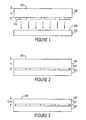
- a wafer (i.e ., a substrate) 100has a thickness (t1) of about 250 microns to about 400 microns.
- a plurality of light emitting devices (LED) 110are formed on a surface of the wafer 100 that is opposite a backside 103 of the wafer 100.
- the plurality of LEDscan be GaN-based light emitting diodes that typically comprise an insulating or semiconducting substrate (or wafer) such as SiC or sapphire on which a plurality of GaN-based epitaxial layers are deposited.
- the epitaxial layerscomprise an active region having a p-n junction that emits light when energized.
- the waferis a SiC wafer of 4H-SiC, 6H-SiC or another type of material known to those skilled in the art.
- a wafer 100(including the plurality of LEDs 110) and a wafer carrier 105 are coupled together via an adhesive layer 120 in contact with the plurality of LEDs so that the entire assembly can be subject to processing by, for example, mounting the wafer carrier 105 in a grinder so that the backside 103 of the wafer 100 can be accessed.
- the wafer 100/plurality of LEDs 110can be coupled to the wafer carrier 105 using any technique known to those skilled in the art, such as a wax, and may be applied to the plurality of LEDs or to the wafer carrier.
- contactincludes direct contact as well as indirect contact where, for example, one or more intervening elements (such as the adhesive layer described above) are present between the plurality of LEDs and the wafer so that these two elements can be coupled together and the backside of the wafer can be processed while holding the carrier.
- intervening elementssuch as the adhesive layer described above
- the backside 103 of the wafer 100is processed to reduce the wafer 100 to a thickness t2, which is less than t1, to form a thinned wafer 100'.
- the thickness t2is less than t1 to allow a saw blade having a beveled tip to cut beneath the surface of the backside 103 to a depth less than about a length of the bevel of the tip of the saw blade. Accordingly, the beveled tip is partially inserted into the backside 103 so that straight edges of the saw blade can remain exposed above the backside 103.
- the thickness of the wafer 100is reduced using a grinder, such as an in-feed or creep feed grinder.
- a grindersuch as an in-feed or creep feed grinder.
- the thickness of the wafer 100is reduced using lapping, chemical or reactive ion etching or combinations of these approaches with or without grinding.
- etchingmay be used to treat the backside of the thinned wafer (i.e. , after thinning the wafer) to reduce damage to the wafer so that growth of epi-layers may be improved.
- the beveled tipmay be inserted farther so that a small portion of the straight edges of the saw blade are inserted below the surface of the thinned wafer 100'.
- the LEDs so formedmay still provide the substantially the same benefits as those embodiments where the beveled tip is partially inserted (such as improved light extraction and improved conformal deposition of a phosphor coating thereon). Accordingly, embodiments where a small portion of the straight edges of the saw blade are inserted below the surface of the thinned wafer 100' will be understood to be within the scope of the claimed subject matter.
- the wafer 100is thinned to a thickness of less than 150 microns. In other embodiments according to the invention, the wafer 100 is thinned to a thickness of less than 120 microns. In some embodiments according to the invention, the wafer 100 is thinned using an in-feed grinder or a creep-feed grinder.
- the wafer carrier 105can be removed from the assembly by, for example, heating the adhesive layer 120 so that the thinned wafer 100' and the plurality of LEDs thereon may be removed as shown in Figure 4 .
- the wafer carrier 105can be removed from the assembly using an appropriate based on the structure used to couple these elements as shown above in reference, for example, to Figure 2 .
- the structuremay be dissolved or melted to separate the wafer carrier 105 from the assembly.
- Ohmic contacts 107can be formed on the backside 103 of the wafer 100' using, for example, laser annealing as discussed in U.S. Patent Application Serial No.: 10/916,113 , entitled Localized Annealing of Metal-Silicon Carbide Ohmic Contacts and Devices So Formed to Slater et al., filed August 11, 2004, which is commonly assigned to the present Assignee.
- the ohmic contactscan be formed on the thinned wafer 100' while the wafer is coupled to the wafer carrier. In some embodiments according to the invention, the ohmic contacts can be formed on the thinned wafer 100' after the wafer is removed from the wafer carrier, as shown for example, in Figure 5 . Bonding pads 106 can be formed on the plurality of LEDs 110 opposite the ohmic contacts. A saw blade 30 can be used to cut the wafer 100' to separate the plurality of LEDs for packaging.
- the saw blade 30can cut through the entire wafer 100' to form straight edges on the thinned wafer 100' between the separated plurality of LEDs 110 or substantially through the thinned wafer 100' so that the LEDs 110 may be separated from one another by applying pressure along the score lines formed by the saw blade 30.
- the saw blade 30is partially inserted into the thinned wafer 100' to a depth that is less than the length of the beveled tip 131 to form beveled grooves 17 in the thinned wafer 100'.
- the saw 30is partially inserted into the thinned wafer 100' so that the straight edges 31 of the saw 30 remain exposed when the beveled tip 131 is partially inserted to avoid the formation of undesirable geometries in the thinned wafer 100' above the beveled grooves 17.
- the thickness of the thinned wafer 100'allows the beveled groves 17 to penetrate sufficiently into the thinned wafer 110' so that the plurality of LEDs can be separated from one another by breaking the thinned wafer 100' along grooves (or score lines) as shown in Figure 7 .
- bonding pads 106 and ohmic contacts 107can be formed on the plurality of LEDs.
- the backside 103 of the wafer 100'can be processed to further improve light extraction from the LED including patterning the backside 103 with a laser or by what is commonly referred to as "roughing.”
- the laser patterningmay be provided in a single or step-wise fashion.
- By patterning the backside 103light extraction may be improved, for example, by providing a randomization pattern thereon.
- Embodiments of the inventionmay be particularly well suited to larger area devices where the effectiveness of angled sidewalls of the wafer 100' may be reduced because of the surface area of the device.
- one or both of the opposing faces of the wafer 100'i.e. , a front side and the backside 103) may be patterned.
- the wafer 100'may be patterned using a laser patterning system such as that described in U.S. Patent Application Serial No. 10/815,293 , entitled Laser Patterning of Light Emitting Devices and Patterned Light Emitting Devices to Donofrio, filed April 1, 2004.
- the laser used to pattern the wafer 100'is an excimer pulsed laser, however any laser system suitable for removing material from the substrate may be used.
- the laser systemcould be a frequency tripled and/or quadrupled YAG laser.
- the laserhas a wavelength of 308 nm, however, other wavelengths, such as 248 nm, 193 nm, 157 nm, 355 nm or 266 nm could also be used.
- assist processes known to those of skill in the artcould also be employed to mitigate surface damage and/or enhance laser absorption, such as water mist and/or assist gases.
- Multiple pulses of the lasermay be used to remove material from the substrate. Any energy suitable for controllably removing material from the substrate may be used.
- a pulsed 308 nm laser of 4.2 J/pulsemay be used in certain embodiments of the present invention.
- Figure 8is a cross-sectional view of an LED on the wafer 100' having the backside 103 laser patterned according to some embodiments of the invention.
- Figure 9is an isometric pictorial view of the light-emitting device of Figure 8 .
- Three-dimensional patterns 120are formed in the backside 103 using a laser as described above.
- the LED 110is formed on an opposite side 104 ( i.e. , front side) of the wafer 100'.
- the patterns 120are surrounded by an uninterrupted perimeter 130 on the backside 103 of the wafer 100.
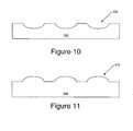
- Figures 10 and 11are cross-sectional views of wafers 100' according to further embodiments of the present invention.
- curved surfaces extending into 200 or protruding 210 from the wafer 100'may be provided by laser patterning.
- the curved surfaces 200, 210may include a parabolic curve. Such a curve may be provided, for example, by controlling the laser light using a series of masks that provided the selective removal of substrate material to provide the parabolic structures.
- the curved surfacesmay provide lenses in the substrate.
- the curved surfacesmay provide a sinusoidal pattern of grooves.
- the wafer 100'could be shaped to a single curve so as to provide a curved wafer 100'.
- the curved wafer 100'may be curved on both faces.
- the light emitting devicecould be provided on the curved surface of the wafer 100'.
- Figures 12 and 13are cross-sectional views of wafers 100' according to further embodiments of the invention. As seen in Figures 12 and 13 , combinations of curved 220 and non-curved features 230, 240 may be provided in a single wafer 100'. Thus, embodiments of the invention may include multiple different three-dimensional geometric patterns in a single wafer 100'.
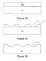
- Figures 14 through 16illustrate alternative embodiments for laser patterning according to some embodiments of the invention.
- a polymer mask layer 300may be provided on the wafer 100'.
- the polymer mask layer 300is laser patterned to provide a polymer mask 310 having three-dimensional features 320 corresponding to features to be provided in the wafer 100'.
- the mask 310is used as an etch mask and the wafer 100' is etched to provide the three-dimensional features 330.
- the etchmay, for example, be a dry etch.
- Conventional polymer masks and techniques for etching using polymer masksmay be used. Additionally, other mask materials that may be laser patterned could also be used.
- the etching maskis a polymer etching mask
- the polymermay be patterned with a 248 nm laser.
- Characteristics of the etching processmay be taken into account in designing the characteristics of the mask 310 to provide a desired three-dimensional geometric pattern in the wafer 100'. For example, the differences in etch rate between the mask material and the silicon carbide wafer may be taken into account when the mask is patterned.
- the shape of the etching maskmay be readily adjusted through control of the laser mask.
- the shape of the etching maskmay take into account the 6 to 1 etching rate of the etching mask to the silicon carbide and the features adjusted accordingly.
- Such an adjustment of mask characteristicsmay be difficult to provide without the use of laser patterning of the etching mask.
- multiple geometries, e.g., pyramids and lensescan be formed in a single step with scanning image technique by designing them into the laser mask.
- the surface of the wafer after the etchmay be rough or smooth.
- a roughened surfacemay be provided, for example, by placing a thin layer of material, such as aluminum, between the etch mask and the substrate to create a micro-mask. When etched, the micro-mask may act to roughen a surface of the wafer 100'.
Landscapes
- Led Devices (AREA)
Abstract
Description
- This invention relates to microelectronic devices, and more particularly, to the fabrication of light emitting diodes (LEDs) and LEDs so formed.
- It is known that the thickness of Silicon-carbide (SiC) substrates in SiC-based light emitting devices can affect the forward voltage needed to operate the devices at a given current level. For example, the SiC-based light emitting diode C450-CB230-E1000 available from Cree, Inc. has a substrate thickness of about 250 µm (+/- 25 µm) and has an associated forward operating voltage of about 3.5 volts at about 20 mA forward operating current. Moreover, reducing the thickness of the SiC substrate of an LED may reduce the forward voltage, which may yield reduced power consumption in such diodes.
- It is also known that many small electronic devices may incorporate individual devices having reduced thicknesses so that the overall thickness of the electronic device may be reduced. For example, manufacturers of cellular phones may use surface-mounted LED chips to reduce the thickness of the component used to backlight a display of the cellular phone. Accordingly, reducing the thickness of the SiC substrate may also allow the device to be used in these types of small electronic devices.
- It is known to form ohmic contacts on SiC at low/room temperature by, for example, implanting ions into a backside of a SiC wafer. However, if an implanted SiC substrate is thinned prior to formation of ohmic contacts, the doped region may be removed during the thinning, which may make the implant superfluous. Accordingly, metals deposited form ohmic contacts may not have ohmic properties when deposited on the substrate as the implant may be performed in a later step. Ion implantation for the formation of ohmic contacts is discussed, for example, in
U. S. Patent Application Serial No. 09/787,189 , and in U.S. Patent Publication No.US 2002/0179910 . - It is also known to form metal ohmic contacts by depositing a metal, such as nickel, and annealing the metal at a high temperature (such as temperatures greater than 900°C). High temperature annealing may damage epitaxial layers of gallium nitride based materials included on the SiC substrate.
- The present invention provides a method of processing a semiconductor wafer to form a light emitting diode according to claim 1, comprising:
- forming a plurality of Light Emitting Diodes (LED) on a semiconductor wafer having a first thickness;
- contacting the plurality of LEDs on the wafer to a surface of a carrier to couple the wafer to the carrier;
- reducing the first thickness of the wafer to a second thickness that is less than the first thickness by processing a backside of the wafer;
- laser patterning the backside surface of the wafer while the water is coupled to the carrier to improve light extraction;
- separating the carrier from the plurality of LEDs on the wafer; and cutting the wafer to separate the plurality of LEDs.
- Preferred embodiments of the invention will be described below with reference to the accompanying drawings wherein:
Figures 1-7 are cross-sectional illustrations but illustrate methods of processing semiconductor wafers according to some embodiments of the invention.Figures 8 and 9 are a cross-sectional view and an isometric view of a light emitting device having a laser patterned wafer according to various embodiments of the invention.Figures 10 through 13 are cross-sectional views of laser patterned wafers according to alternative embodiments of the invention.Figures 14 through 16 are cross-sectional view illustrating operations according to laser patterning techniques according to alternative embodiments of the invention.- In some embodiments according to the invention, the first thickness is from 250 µm to 400 µm. In some embodiments according to the invention, reducing the first thickness of the wafer includes grinding, lapping, and/or etching the backside of the wafer to reduce the first thickness of the wafer to the second thickness of less than 150 µm. In some embodiments according to the invention, reducing the first thickness of the wafer includes grinding, lapping, and/or etching the backside of the wafer to reduce the first thickness of the wafer to the second thickness of less than 120 µm. In some embodiments according to the invention, grinding the backside of the wafer includes grinding the backside of the wafer using an in-feed grinder or a creep feed grinder.
- In some embodiments according to the invention, cutting the wafer includes cutting the wafer using a saw blade to form straight edges on the separated plurality of LEDs. In some embodiments according to the invention, cutting the wafer includes cutting score lines on the wafer to form beveled grooves between the plurality of LEDs on the wafer and separating the plurality of LEDs on the wafer from one another along the score lines. In some embodiments according to the invention, cutting the wafer includes cutting the wafer with a saw blade to depth beneath a surface of the wafer of less than about a length of a beveled tip of the saw blade. In some embodiments according to the invention, the depth is less than 120 µm.
- In some embodiments according to the invention, processing includes etching the backside surface. In some embodiments according to the invention, processing includes laser patterning the backside surface.
- In some embodiments according to the invention, separating the carrier from the plurality of LEDs on the wafer includes heating, dissolving, or melting an adhesive layer sufficient to cause separation of the plurality of LEDs from the carrier. In some embodiments according to the invention, the wafer is a Silicon Carbide or sapphire wafer.
- In some embodiments according to the invention, a light emitting device (LED) on a Silicon Carbide (SiC) substrate has a first thickness of less than 150 µm. In some embodiments according to the invention, a forward voltage associated with the SiC substrate is about 3.4 volts. In some embodiments according to the invention, the SiC substrate is 4H-SiC or 6H-SiC.
- The invention now will be described more fully hereinafter with reference to the accompanying drawings, in which embodiments of the invention are shown. However, this invention should not be construed as limited to the embodiments set forth herein. Rather, these embodiments are provided so that this disclosure will be thorough and complete, and will fully convey the scope of the invention to those skilled in the art. In the drawings, the thickness of layers and regions are exaggerated for clarity. Like numbers refer to like elements throughout. As used herein the term "and/or" includes any and all combinations of one or more of the associated listed items.
- The terminology used herein is for the purpose of describing particular embodiments only and is not intended to be limiting of the invention. As used herein, the singular forms "a", "an" and "the" are intended to include the plural forms as well, unless the context clearly indicates otherwise. It will be further understood that the terms "comprises" and/or "comprising," when used in this specification, specify the presence of stated features, integers, steps, operations, elements, and/or components, but do not preclude the presence or addition of one or more other features, integers, steps, operations, elements, components, and/or groups thereof.
- It will be understood that when an element such as a layer, region or substrate is referred to as being "on" or extending "onto" another element, it can be directly on or extend directly onto the other element or intervening elements may also be present. In contrast, when an element is referred to as being "directly on" or extending "directly onto" another element, there are no intervening elements present. It will also be understood that when an element is referred to as being "connected" or "coupled" to another element, it can be directly connected or coupled to the other element or intervening elements may be present. In contrast, when an element is referred to as being "directly connected" or "directly coupled" to another element, there are no intervening elements present. Like numbers refer to like elements throughout the specification.
- It will be understood that, although the terms first, second, etc. may be used herein to describe various elements, components, regions, layers and/or sections, these elements, components, regions, layers and/or sections should not be limited by these terms. These terms are only used to distinguish one element, component, region, layer or section from another region, layer or section. Thus, a first element, component, region, layer or section discussed below could be termed a second element, component, region, layer or section without departing from the teachings of the present invention.
- Furthermore, relative terms, such as "lower" or "bottom" and "upper" or "top," may be used herein to describe one element's relationship to another elements as illustrated in the Figures. It will be understood that relative terms are intended to encompass different orientations of the device in addition to the orientation depicted in the Figures. For example, if the device in the Figures is turned over, elements described as being on the "lower" side of other elements would then be oriented on "upper" sides of the other elements. The exemplary term "lower", can therefore, encompasses both an orientation of "lower" and "upper," depending on the particular orientation of the figure. Similarly, if the device in one of the figures is turned over, elements described as "below" or "beneath" other elements would then be oriented "above" the other elements. The exemplary terms "below" or "beneath" can, therefore, encompass both an orientation of above and below.
- Embodiments of the present invention are described herein with reference to cross-section (and/or plan view) illustrations that are schematic illustrations of idealized embodiments of the present invention. As such, variations from the shapes of the illustrations as a result, for example, of manufacturing techniques and/or tolerances, are to be expected. Thus, embodiments of the present invention should not be construed as limited to the particular shapes of regions illustrated herein but are to include deviations in shapes that result, for example, from manufacturing. For example, an etched region illustrated or described as a rectangle will, typically, have rounded or curved features. Thus, the regions illustrated in the figures are schematic in nature and their shapes are not intended to illustrate the precise shape of a region of a device and are not intended to limit the scope of the present invention.
- Unless otherwise defined, all terms (including technical and scientific terms) used herein have the same meaning as commonly understood by one of ordinary skill in the art to which this invention belongs. It will be further understood that terms, such as those defined in commonly used dictionaries, should be interpreted as having a meaning that is consistent with their meaning in the context of the relevant art and will not be interpreted in an idealized or overly formal sense unless expressly so defined herein. It will also be appreciated by those of skill in the art that references to a structure or feature that is disposed "adjacent" another feature may have portions that overlap or underlie the adjacent feature.
- As used herein the term "ohmic contact" refers to contacts where an impedance associated therewith is substantially given by the relationship of Impedance = V/I, where V is a voltage across the contact and I is the current, at substantially all expected operating frequencies (i.e., the impedance associated with the ohmic contact is substantially the same at all operating frequencies). For example, in some embodiments according to the invention, an ohmic contact can be a contact with a specific contact resistivity of less than about 10 e -03 ohm-cm2 and, in some embodiments less than about 10 e -04 ohm-cm2. Thus, a contact that is rectifying or that has a high specific contact resistivity, for example, a specific contact resistivity of greater than about 10 e -03 ohm-cm2, is not an ohmic contact as that term is used herein.
- Light emitting devices (LEDs) described herein may include a light emitting diode, laser diode and/or other semiconductor device which includes one or more semiconductor layers, which may include silicon, silicon carbide, gallium nitride and/or other semiconductor materials, a substrate which may include sapphire, silicon, silicon carbide, GaN and/or other microelectronic substrates, and one or more contact layers which may include metal and/or other conductive layers. In some embodiments, ultraviolet, blue and/or green LEDs may be provided.
- It will be understood by those having skill in the art that many embodiments of the invention maybe employed with many different combinations of substrate and epitaxial layers. For example, other combinations can include AlGalnP diodes on GaP substrates; InGaAs diodes on GaAs substrates; AlGaAs diodes on GaAs substrates; Silicon Carbide (SiC) diodes on SiC or sapphire (Al203) substrate; and/or nitride-based diodes on gallium nitride, silicon carbide, aluminum nitride, sapphire, zinc oxide and/or other substrates.
- In particular, the LEDs may be devices manufactured and sold by Cree, Inc. of Durham, North Carolina. The invention may be suitable for use with LEDs and/or lasers as described in United States Patent Nos.
6,201,262 ;6,187,606 ;6,120,600 ;5,912,477 ;5,739,554 ;5,631,190 ;5,604,135 ;5,523,589 ;5,416,342 ;5,393,993 ;5,338,944 ;5,210,051 ;5,027,168 ;5,027,168 ;4,966,862 and/or4,918,497 . Other suitable LEDs and/or lasers are described in published U.S. Patent Publication No.US 2003/0006418 A1 entitledGroup III Nitride Based Light Emitting Diode Structures With a Quantum Well and Superlattice, Group III Nitride Based Quantum Well Structures and Group III Nitride Based Superlattice Structures, published January 9, 2003, as well as published U.S. Patent Publication No.US 2002/0123164 A1 entitledLight Emitting Diodes Including Modifications for Light Extraction and Manufacturing Methods Therefor. Furthermore, phosphor coated LEDs, such as those described in U.S. Patent Publication No.US 2004/0056260 , entitledPhosphor-Coated Light Emitting Diodes Including Tapered Sidewalls and Fabrication Methods Therefor, filed September 9, 2003, The LEDs and/or lasers may be configured to operate such that light emission occurs through the substrate. In such embodiments, the substrate may be patterned so as to enhance light output of the devices as is described, for example, in the above-cited U.S. Patent Publication No.US 2002/0123164 A1 . - As described herein below in greater detail, embodiments according to the invention can provide methods of processing semiconductor wafers of light emitting devices by, for example, reducing a thickness of the wafer having light emitting devices (LEDs) mounted thereon by processing the wafer from a backside thereof. The wafer can be thinned to a thickness that allows a partially inserted beveled tip of a saw blade to cut beneath the surface of the wafer sufficiently deep to allow the plurality of LEDs thereon to be separated from one another by breaking the remaining uncut portion of the wafer. In particular, the wafer may be cut to a level beneath the surface that is less than the length of the beveled tip of the saw blade so that straight edges of the saw blade remain exposed (or above) the surface of the wafer. In other words, the partial insertion of the beveled tip of the saw blade may cut deep enough into the wafer to allow the plurality of LEDs to be separated from one another by breaking the wafer along the score lines formed by the partial insertion of the beveled tip.
- Therefore, the
backside 103 of the wafer 100' can be thinned sufficiently to allow the plurality of LEDs on the wafer to be separated from one another by partial insertion of the beveled tip of the saw blade. Partially inserting the beveled tip of the saw blade can avoid the formation of otherwise detrimental geometries while still allowing the plurality to be separated from one another due to the reduced thinness of the wafer. - As shown in
Figure 1 , a wafer (i.e., a substrate) 100 has a thickness (t1) of about 250 microns to about 400 microns. A plurality of light emitting devices (LED) 110 are formed on a surface of thewafer 100 that is opposite abackside 103 of thewafer 100. It will be understood that the plurality of LEDs can be GaN-based light emitting diodes that typically comprise an insulating or semiconducting substrate (or wafer) such as SiC or sapphire on which a plurality of GaN-based epitaxial layers are deposited. The epitaxial layers comprise an active region having a p-n junction that emits light when energized. In some embodiments according to the invention, the wafer is a SiC wafer of 4H-SiC, 6H-SiC or another type of material known to those skilled in the art. - According to
Figure 2 , in some embodiments according to the invention, a wafer 100 (including the plurality of LEDs 110) and awafer carrier 105 are coupled together via anadhesive layer 120 in contact with the plurality of LEDs so that the entire assembly can be subject to processing by, for example, mounting thewafer carrier 105 in a grinder so that thebackside 103 of thewafer 100 can be accessed. It will be understood that thewafer 100/plurality ofLEDs 110 can be coupled to thewafer carrier 105 using any technique known to those skilled in the art, such as a wax, and may be applied to the plurality of LEDs or to the wafer carrier. It will be further understood that the term "contact" includes direct contact as well as indirect contact where, for example, one or more intervening elements (such as the adhesive layer described above) are present between the plurality of LEDs and the wafer so that these two elements can be coupled together and the backside of the wafer can be processed while holding the carrier. - According to
Figure 3 , in some embodiments according to the invention, thebackside 103 of thewafer 100 is processed to reduce thewafer 100 to a thickness t2, which is less than t1, to form a thinned wafer 100'. It will be understood that the thickness t2 is less than t1 to allow a saw blade having a beveled tip to cut beneath the surface of thebackside 103 to a depth less than about a length of the bevel of the tip of the saw blade. Accordingly, the beveled tip is partially inserted into thebackside 103 so that straight edges of the saw blade can remain exposed above thebackside 103. - In some embodiments according to the invention, the thickness of the
wafer 100 is reduced using a grinder, such as an in-feed or creep feed grinder. In other embodiments according to the invention, the thickness of thewafer 100 is reduced using lapping, chemical or reactive ion etching or combinations of these approaches with or without grinding. In still other embodiments according to the invention, etching may be used to treat the backside of the thinned wafer (i.e., after thinning the wafer) to reduce damage to the wafer so that growth of epi-layers may be improved. - It will be understood that although the embodiments described above refer to partial insertion of the beveled tip (so that the straight edges of the saw blade can remain exposed), in some embodiments according to the invention, the beveled tip may be inserted farther so that a small portion of the straight edges of the saw blade are inserted below the surface of the thinned wafer 100'. It will be further understood that the LEDs so formed may still provide the substantially the same benefits as those embodiments where the beveled tip is partially inserted (such as improved light extraction and improved conformal deposition of a phosphor coating thereon). Accordingly, embodiments where a small portion of the straight edges of the saw blade are inserted below the surface of the thinned wafer 100' will be understood to be within the scope of the claimed subject matter.
- In some embodiments according to the invention, the
wafer 100 is thinned to a thickness of less than 150 microns. In other embodiments according to the invention, thewafer 100 is thinned to a thickness of less than 120 microns. In some embodiments according to the invention, thewafer 100 is thinned using an in-feed grinder or a creep-feed grinder. - The partial insertion of the beveled tip coupled with the reduced thickness of the thinned wafer 100' allows the plurality of LEDs to be separated from one another by, for example, breaking the thinned wafer 100' rather than cutting through the entire wafer. Once the
backside 103 has been processed to sufficiently thin the wafer 100', thewafer carrier 105 can be removed from the assembly by, for example, heating theadhesive layer 120 so that the thinned wafer 100' and the plurality of LEDs thereon may be removed as shown inFigure 4 . In other embodiments according to the invention, thewafer carrier 105 can be removed from the assembly using an appropriate based on the structure used to couple these elements as shown above in reference, for example, toFigure 2 . For example, the structure may be dissolved or melted to separate thewafer carrier 105 from the assembly. Ohmic contacts 107 can be formed on thebackside 103 of the wafer 100' using, for example, laser annealing as discussed inU.S. Patent Application Serial No.: 10/916,113 - It will be understood that the ohmic contacts can be formed on the thinned wafer 100' while the wafer is coupled to the wafer carrier. In some embodiments according to the invention, the ohmic contacts can be formed on the thinned wafer 100' after the wafer is removed from the wafer carrier, as shown for example, in
Figure 5 .Bonding pads 106 can be formed on the plurality ofLEDs 110 opposite the ohmic contacts. Asaw blade 30 can be used to cut the wafer 100' to separate the plurality of LEDs for packaging. It will be understood that thesaw blade 30 can cut through the entire wafer 100' to form straight edges on the thinned wafer 100' between the separated plurality ofLEDs 110 or substantially through the thinned wafer 100' so that theLEDs 110 may be separated from one another by applying pressure along the score lines formed by thesaw blade 30. - In other embodiments according to the invention as illustrated in
Figure 6 , thesaw blade 30 is partially inserted into the thinned wafer 100' to a depth that is less than the length of thebeveled tip 131 to formbeveled grooves 17 in the thinned wafer 100'. Thesaw 30 is partially inserted into the thinned wafer 100' so that thestraight edges 31 of thesaw 30 remain exposed when thebeveled tip 131 is partially inserted to avoid the formation of undesirable geometries in the thinned wafer 100' above thebeveled grooves 17. Moreover, the thickness of the thinned wafer 100' allows thebeveled groves 17 to penetrate sufficiently into the thinned wafer 110' so that the plurality of LEDs can be separated from one another by breaking the thinned wafer 100' along grooves (or score lines) as shown inFigure 7 . Furthermore, as discussed above in reference toFigure 5 ,bonding pads 106 andohmic contacts 107 can be formed on the plurality of LEDs. - In further aspects according to embodiments of the invention, the
backside 103 of the wafer 100' can be processed to further improve light extraction from the LED including patterning thebackside 103 with a laser or by what is commonly referred to as "roughing." The laser patterning may be provided in a single or step-wise fashion. By patterning thebackside 103, light extraction may be improved, for example, by providing a randomization pattern thereon. Embodiments of the invention may be particularly well suited to larger area devices where the effectiveness of angled sidewalls of the wafer 100' may be reduced because of the surface area of the device. Furthermore, one or both of the opposing faces of the wafer 100' (i.e., a front side and the backside 103) may be patterned. The wafer 100' may be patterned using a laser patterning system such as that described inU.S. Patent Application Serial No. 10/815,293 - In some embodiments of the invention, the laser used to pattern the wafer 100' is an excimer pulsed laser, however any laser system suitable for removing material from the substrate may be used. For example, the laser system could be a frequency tripled and/or quadrupled YAG laser. In certain embodiments of the invention, the laser has a wavelength of 308 nm, however, other wavelengths, such as 248 nm, 193 nm, 157 nm, 355 nm or 266 nm could also be used. Additionally, assist processes known to those of skill in the art could also be employed to mitigate surface damage and/or enhance laser absorption, such as water mist and/or assist gases. Multiple pulses of the laser may be used to remove material from the substrate. Any energy suitable for controllably removing material from the substrate may be used. For example, a pulsed 308 nm laser of 4.2 J/pulse may be used in certain embodiments of the present invention.
Figure 8 is a cross-sectional view of an LED on the wafer 100' having thebackside 103 laser patterned according to some embodiments of the invention.Figure 9 is an isometric pictorial view of the light-emitting device ofFigure 8 . Three-dimensional patterns 120 are formed in thebackside 103 using a laser as described above. In the embodiments illustrated inFigures 8 and 9 , theLED 110 is formed on an opposite side 104 (i.e., front side) of the wafer 100'. As is seen inFigures 8 and 9 , thepatterns 120 are surrounded by anuninterrupted perimeter 130 on thebackside 103 of thewafer 100.Figures 10 and 11 are cross-sectional views of wafers 100' according to further embodiments of the present invention. As seen inFigures 10 and 11 , in cross-section, curved surfaces extending into 200 or protruding 210 from the wafer 100' may be provided by laser patterning. Thecurved surfaces - While multiple curved structures are illustrated in
Figures 10 and 11 , the wafer 100' could be shaped to a single curve so as to provide a curved wafer 100'. The curved wafer 100' may be curved on both faces. Also, the light emitting device could be provided on the curved surface of the wafer 100'. Figures 12 and 13 are cross-sectional views of wafers 100' according to further embodiments of the invention. As seen inFigures 12 and 13 , combinations of curved 220 andnon-curved features Figures 14 through 16 illustrate alternative embodiments for laser patterning according to some embodiments of the invention. As seen inFigure 14 , apolymer mask layer 300 may be provided on the wafer 100'. InFigure 15 , thepolymer mask layer 300 is laser patterned to provide apolymer mask 310 having three-dimensional features 320 corresponding to features to be provided in the wafer 100'. InFigure 16 , themask 310 is used as an etch mask and the wafer 100' is etched to provide the three-dimensional features 330. The etch may, for example, be a dry etch. Conventional polymer masks and techniques for etching using polymer masks may be used. Additionally, other mask materials that may be laser patterned could also be used.- Techniques for laser patterning a polymer layer are known to those of skill in the art. For example, such techniques are described in "Laser micro-machining of high density optical structures on large substrates" by Boehlenet al. of Exitech Ltd.In particular embodiments of the invention, where the etching mask is a polymer etching mask, the polymer may be patterned with a 248 nm laser.
Characteristics of the etching process may be taken into account in designing the characteristics of themask 310 to provide a desired three-dimensional geometric pattern in the wafer 100'. For example, the differences in etch rate between the mask material and the silicon carbide wafer may be taken into account when the mask is patterned. - Because the patterning of the etching mask is provided for by laser patterning, the shape of the etching mask may be readily adjusted through control of the laser mask. Thus, for example, the shape of the etching mask may take into account the 6 to 1 etching rate of the etching mask to the silicon carbide and the features adjusted accordingly. Such an adjustment of mask characteristics may be difficult to provide without the use of laser patterning of the etching mask. Furthermore, through utilization of laser patterning, multiple geometries, e.g., pyramids and lenses can be formed in a single step with scanning image technique by designing them into the laser mask.
- Additionally, the surface of the wafer after the etch may be rough or smooth.
A roughened surface may be provided, for example, by placing a thin layer of material, such as aluminum, between the etch mask and the substrate to create a micro-mask. When etched, the micro-mask may act to roughen a surface of the wafer 100'.
Claims (15)
- A method of processing a semiconductor wafer to form a light emitting diode, comprising:forming a plurality of Light Emitting Diodes, LEDs, (110) on a semiconductor wafer having a first thickness (t1);contacting the plurality of LEDs on the wafer to a surface of a carrier (105) to couple the wafer to the carrier;reducing the first thickness (t1) of the wafer to a second thickness (t2) that is less than the first thickness by processing a backside (103) of the wafer; laser patterning the backside surface of the wafer while the wafer is coupled to the carrier to improve light extraction;separating the carrier from the plurality of LEDs on the wafer; andcutting the wafer to separate the plurality of LEDs.
- A method according to claim 1, further comprising:forming a plurality of respective contacts on the backside surface while the wafer is coupled to the carrier, opposite where respective bonding pads are to be formed on the plurality of LEDs.
- A method according to Claim 1 wherein the first thickness comprises a thickness from 250 µm to 400 µm.
- A method according to any preceding Claim wherein reducing the first thickness of the wafer (100) comprises grinding, lapping, and/or etching the backside (103) of the wafer to reduce the first thickness (t1) of the wafer to the second thickness (t2) of less than 150 µm.
- A method according to Claim 4 wherein grinding the backside (103) of the wafer (100) comprises grinding the backside of the wafer using an in-feed grinder or a creep feed grinder.
- A method according to any preceding Claim wherein cutting the wafer comprises cutting the wafer using a saw blade (30) to form straight edges on the separated plurality of LEDs.
- A method according to any preceding Claim wherein cutting the wafer comprises:cutting score lines on the wafer to form beveled grooves (17) between the plurality of LEDs (110) on the wafer; andseparating the plurality of LEDs on the wafer from one another along the score lines.
- A method according to any preceding Claim wherein cutting the wafer comprises cutting the wafer with a saw blade (30) having a beveled tip (131) to a depth beneath a surface of the wafer of less than about a length of the beveled tip of the saw blade.
- A method according to Claim 7 wherein the depth comprises less than 120 µm.
- A method according to any preceding Claim wherein separating the carrier from the plurality of LEDs on the wafer comprises heating, melting or dissolving an adhesive layer sufficient to cause separation of the plurality of LEDs from the carrier.
- A method according to any preceding Claim wherein the wafer comprises a Silicon Carbide or sapphire wafer.
- A method according to any preceding Claim wherein processing comprises etching the backside surface (103).
- A method according to Claim 2 wherein forming a plurality of respective contacts comprises forming a plurality of ohmic contacts using laser annealing.
- A method according to any preceding claim, wherein the patterning the backside comprises forming three dimensional patterns (220, 230, 240) on the backside.
- A method according to claim 13, wherein the three dimensional patterns are formed using a laser.
Applications Claiming Priority (3)
| Application Number | Priority Date | Filing Date | Title |
|---|---|---|---|
| US51939603P | 2003-11-12 | 2003-11-12 | |
| PCT/US2004/037934WO2005048363A2 (en) | 2003-11-12 | 2004-11-12 | Methods of processing semiconductor wafer backsides having light emitting devices (leds) thereon and leds so formed |
| US10/987,135US7291529B2 (en) | 2003-11-12 | 2004-11-12 | Methods of processing semiconductor wafer backsides having light emitting devices (LEDs) thereon |
Publications (2)
| Publication Number | Publication Date |
|---|---|
| EP1690301A2 EP1690301A2 (en) | 2006-08-16 |
| EP1690301B1true EP1690301B1 (en) | 2012-08-15 |
Family
ID=34594959
Family Applications (1)
| Application Number | Title | Priority Date | Filing Date |
|---|---|---|---|
| EP04810913AExpired - LifetimeEP1690301B1 (en) | 2003-11-12 | 2004-11-12 | Methods of processing semiconductor wafer backsides having light emitting diodes (leds) thereon |
Country Status (6)
| Country | Link |
|---|---|
| US (1) | US7291529B2 (en) |
| EP (1) | EP1690301B1 (en) |
| JP (1) | JP2007511105A (en) |
| KR (1) | KR20060131774A (en) |
| CA (1) | CA2545628A1 (en) |
| WO (1) | WO2005048363A2 (en) |
Families Citing this family (60)
| Publication number | Priority date | Publication date | Assignee | Title |
|---|---|---|---|---|
| EP1690301B1 (en)* | 2003-11-12 | 2012-08-15 | Cree, Inc. | Methods of processing semiconductor wafer backsides having light emitting diodes (leds) thereon |
| US7419912B2 (en) | 2004-04-01 | 2008-09-02 | Cree, Inc. | Laser patterning of light emitting devices |
| WO2006031641A2 (en)* | 2004-09-10 | 2006-03-23 | Cree, Inc. | Method of manufacturing carrier wafer and resulting carrier wafer structures |
| DE102004061865A1 (en)* | 2004-09-29 | 2006-03-30 | Osram Opto Semiconductors Gmbh | Process for producing a thin-film semiconductor chip |
| NL1029688C2 (en)* | 2005-08-05 | 2007-02-06 | Lemnis Lighting Ip Gmbh | Method for manufacturing an electrical circuit provided with a plurality of LEDs. |
| KR100621154B1 (en)* | 2005-08-26 | 2006-09-07 | 서울반도체 주식회사 | Light emitting diode manufacturing method |
| EP2546865B1 (en)* | 2005-09-16 | 2023-12-06 | Wolfspeed, Inc. | Methods of processing semiconductor wafers having silicon carbide power devices thereon |
| US7772604B2 (en) | 2006-01-05 | 2010-08-10 | Illumitex | Separate optical device for directing light from an LED |
| US8264138B2 (en) | 2006-01-20 | 2012-09-11 | Cree, Inc. | Shifting spectral content in solid state light emitters by spatially separating lumiphor films |
| US8441179B2 (en) | 2006-01-20 | 2013-05-14 | Cree, Inc. | Lighting devices having remote lumiphors that are excited by lumiphor-converted semiconductor excitation sources |
| US8698184B2 (en) | 2011-01-21 | 2014-04-15 | Cree, Inc. | Light emitting diodes with low junction temperature and solid state backlight components including light emitting diodes with low junction temperature |
| US8432012B2 (en) | 2006-08-01 | 2013-04-30 | Cree, Inc. | Semiconductor devices including schottky diodes having overlapping doped regions and methods of fabricating same |
| US7728402B2 (en) | 2006-08-01 | 2010-06-01 | Cree, Inc. | Semiconductor devices including schottky diodes with controlled breakdown |
| KR101529331B1 (en) | 2006-08-17 | 2015-06-16 | 크리 인코포레이티드 | High power insulated gate bipolar transistors |
| EP2060155A2 (en) | 2006-08-23 | 2009-05-20 | Cree Led Lighting Solutions, Inc. | Lighting device and lighting method |
| KR101262386B1 (en) | 2006-09-25 | 2013-05-08 | 엘지이노텍 주식회사 | Method for manufacturing nitride semiconductor light emitting device |
| WO2008042351A2 (en) | 2006-10-02 | 2008-04-10 | Illumitex, Inc. | Led system and method |
| US8835987B2 (en) | 2007-02-27 | 2014-09-16 | Cree, Inc. | Insulated gate bipolar transistors including current suppressing layers |
| US8866150B2 (en)* | 2007-05-31 | 2014-10-21 | Cree, Inc. | Silicon carbide power devices including P-type epitaxial layers and direct ohmic contacts |
| US7863635B2 (en) | 2007-08-07 | 2011-01-04 | Cree, Inc. | Semiconductor light emitting devices with applied wavelength conversion materials |
| US7687825B2 (en)* | 2007-09-18 | 2010-03-30 | Cree, Inc. | Insulated gate bipolar conduction transistors (IBCTS) and related methods of fabrication |
| JP2011501466A (en)* | 2007-10-26 | 2011-01-06 | クリー エル イー ディー ライティング ソリューションズ インコーポレイテッド | Lighting device having one or more light emitters and method of making the same |
| JP2011512037A (en) | 2008-02-08 | 2011-04-14 | イルミテックス, インコーポレイテッド | System and method for emitter layer shaping |
| US8232558B2 (en) | 2008-05-21 | 2012-07-31 | Cree, Inc. | Junction barrier Schottky diodes with current surge capability |
| TW201034256A (en) | 2008-12-11 | 2010-09-16 | Illumitex Inc | Systems and methods for packaging light-emitting diode devices |
| US8187983B2 (en)* | 2009-04-16 | 2012-05-29 | Micron Technology, Inc. | Methods for fabricating semiconductor components using thinning and back side laser processing |
| US8294507B2 (en) | 2009-05-08 | 2012-10-23 | Cree, Inc. | Wide bandgap bipolar turn-off thyristor having non-negative temperature coefficient and related control circuits |
| US8921876B2 (en) | 2009-06-02 | 2014-12-30 | Cree, Inc. | Lighting devices with discrete lumiphor-bearing regions within or on a surface of remote elements |
| US8193848B2 (en) | 2009-06-02 | 2012-06-05 | Cree, Inc. | Power switching devices having controllable surge current capabilities |
| US8629509B2 (en) | 2009-06-02 | 2014-01-14 | Cree, Inc. | High voltage insulated gate bipolar transistors with minority carrier diverter |
| DE102009032486A1 (en)* | 2009-07-09 | 2011-01-13 | Osram Opto Semiconductors Gmbh | Optoelectronic component |
| US8541787B2 (en) | 2009-07-15 | 2013-09-24 | Cree, Inc. | High breakdown voltage wide band-gap MOS-gated bipolar junction transistors with avalanche capability |
| US8449128B2 (en) | 2009-08-20 | 2013-05-28 | Illumitex, Inc. | System and method for a lens and phosphor layer |
| US8585253B2 (en) | 2009-08-20 | 2013-11-19 | Illumitex, Inc. | System and method for color mixing lens array |
| US8354690B2 (en) | 2009-08-31 | 2013-01-15 | Cree, Inc. | Solid-state pinch off thyristor circuits |
| US9275979B2 (en) | 2010-03-03 | 2016-03-01 | Cree, Inc. | Enhanced color rendering index emitter through phosphor separation |
| US9117739B2 (en) | 2010-03-08 | 2015-08-25 | Cree, Inc. | Semiconductor devices with heterojunction barrier regions and methods of fabricating same |
| US8415671B2 (en) | 2010-04-16 | 2013-04-09 | Cree, Inc. | Wide band-gap MOSFETs having a heterojunction under gate trenches thereof and related methods of forming such devices |
| DE102010027679A1 (en) | 2010-07-20 | 2012-01-26 | Osram Opto Semiconductors Gmbh | Optoelectronic component |
| JP5643036B2 (en)* | 2010-09-14 | 2014-12-17 | 株式会社ディスコ | Processing method of optical device wafer |
| US11251164B2 (en) | 2011-02-16 | 2022-02-15 | Creeled, Inc. | Multi-layer conversion material for down conversion in solid state lighting |
| TWI452691B (en)* | 2011-04-25 | 2014-09-11 | Univ Nat Cheng Kung | Semiconductor structure and method for making the same, and method for forming epitaxial semi-finished product |
| US9142662B2 (en) | 2011-05-06 | 2015-09-22 | Cree, Inc. | Field effect transistor devices with low source resistance |
| US9673283B2 (en) | 2011-05-06 | 2017-06-06 | Cree, Inc. | Power module for supporting high current densities |
| US9029945B2 (en) | 2011-05-06 | 2015-05-12 | Cree, Inc. | Field effect transistor devices with low source resistance |
| US9640617B2 (en) | 2011-09-11 | 2017-05-02 | Cree, Inc. | High performance power module |
| US8618582B2 (en) | 2011-09-11 | 2013-12-31 | Cree, Inc. | Edge termination structure employing recesses for edge termination elements |
| US8680587B2 (en) | 2011-09-11 | 2014-03-25 | Cree, Inc. | Schottky diode |
| US8664665B2 (en) | 2011-09-11 | 2014-03-04 | Cree, Inc. | Schottky diode employing recesses for elements of junction barrier array |
| US9373617B2 (en) | 2011-09-11 | 2016-06-21 | Cree, Inc. | High current, low switching loss SiC power module |
| JP2014011244A (en)* | 2012-06-28 | 2014-01-20 | Nitto Denko Corp | Led manufacturing method |
| US20190237644A1 (en)* | 2018-01-30 | 2019-08-01 | Mikro Mesa Technology Co., Ltd. | Light emitting device with multi-layer isolation structure |
| US10971612B2 (en) | 2019-06-13 | 2021-04-06 | Cree, Inc. | High electron mobility transistors and power amplifiers including said transistors having improved performance and reliability |
| US10923585B2 (en) | 2019-06-13 | 2021-02-16 | Cree, Inc. | High electron mobility transistors having improved contact spacing and/or improved contact vias |
| US11769768B2 (en) | 2020-06-01 | 2023-09-26 | Wolfspeed, Inc. | Methods for pillar connection on frontside and passive device integration on backside of die |
| US12009417B2 (en) | 2021-05-20 | 2024-06-11 | Macom Technology Solutions Holdings, Inc. | High electron mobility transistors having improved performance |
| US12015075B2 (en) | 2021-05-20 | 2024-06-18 | Macom Technology Solutions Holdings, Inc. | Methods of manufacturing high electron mobility transistors having a modified interface region |
| US11842937B2 (en) | 2021-07-30 | 2023-12-12 | Wolfspeed, Inc. | Encapsulation stack for improved humidity performance and related fabrication methods |
| US12218202B2 (en) | 2021-09-16 | 2025-02-04 | Wolfspeed, Inc. | Semiconductor device incorporating a substrate recess |
| WO2024240564A1 (en)* | 2023-05-25 | 2024-11-28 | Ams-Osram International Gmbh | Optoelectronic semiconductor chip and corresponding production method |
Citations (1)
| Publication number | Priority date | Publication date | Assignee | Title |
|---|---|---|---|---|
| US6610551B1 (en)* | 1998-09-16 | 2003-08-26 | Cree, Inc. | Vertical geometry InGaN LED |
Family Cites Families (38)
| Publication number | Priority date | Publication date | Assignee | Title |
|---|---|---|---|---|
| US5027168A (en) | 1988-12-14 | 1991-06-25 | Cree Research, Inc. | Blue light emitting diode formed in silicon carbide |
| US4918497A (en) | 1988-12-14 | 1990-04-17 | Cree Research, Inc. | Blue light emitting diode formed in silicon carbide |
| US5087949A (en) | 1989-06-27 | 1992-02-11 | Hewlett-Packard Company | Light-emitting diode with diagonal faces |
| EP0405757A3 (en)* | 1989-06-27 | 1991-01-30 | Hewlett-Packard Company | High efficiency light-emitting diode |
| US4966862A (en) | 1989-08-28 | 1990-10-30 | Cree Research, Inc. | Method of production of light emitting diodes |
| US5210051A (en) | 1990-03-27 | 1993-05-11 | Cree Research, Inc. | High efficiency light emitting diodes from bipolar gallium nitride |
| JP2914014B2 (en)* | 1992-06-05 | 1999-06-28 | 日亜化学工業株式会社 | Method of manufacturing gallium nitride based compound semiconductor chip |
| US5416342A (en) | 1993-06-23 | 1995-05-16 | Cree Research, Inc. | Blue light-emitting diode with high external quantum efficiency |
| US5338944A (en) | 1993-09-22 | 1994-08-16 | Cree Research, Inc. | Blue light-emitting diode with degenerate junction structure |
| US5393993A (en) | 1993-12-13 | 1995-02-28 | Cree Research, Inc. | Buffer structure between silicon carbide and gallium nitride and resulting semiconductor devices |
| US5604135A (en) | 1994-08-12 | 1997-02-18 | Cree Research, Inc. | Method of forming green light emitting diode in silicon carbide |
| US5523589A (en) | 1994-09-20 | 1996-06-04 | Cree Research, Inc. | Vertical geometry light emitting diode with group III nitride active layer and extended lifetime |
| US5631190A (en) | 1994-10-07 | 1997-05-20 | Cree Research, Inc. | Method for producing high efficiency light-emitting diodes and resulting diode structures |
| US5739554A (en) | 1995-05-08 | 1998-04-14 | Cree Research, Inc. | Double heterojunction light emitting diode with gallium nitride active layer |
| US5994205A (en) | 1997-02-03 | 1999-11-30 | Kabushiki Kaisha Toshiba | Method of separating semiconductor devices |
| US6201262B1 (en) | 1997-10-07 | 2001-03-13 | Cree, Inc. | Group III nitride photonic devices on silicon carbide substrates with conductive buffer interlay structure |
| JP2000022213A (en) | 1998-06-30 | 2000-01-21 | Sharp Corp | Gallium nitride based semiconductor device and manufacturing method thereof |
| JP2000091636A (en)* | 1998-09-07 | 2000-03-31 | Rohm Co Ltd | Manufacturing method of semiconductor light emitting device |
| US6884644B1 (en)* | 1998-09-16 | 2005-04-26 | Cree, Inc. | Low temperature formation of backside ohmic contacts for vertical devices |
| US6803243B2 (en) | 2001-03-15 | 2004-10-12 | Cree, Inc. | Low temperature formation of backside ohmic contacts for vertical devices |
| JP4137310B2 (en)* | 1999-09-06 | 2008-08-20 | リンテック株式会社 | Method and apparatus for peeling articles fixed to double-sided pressure-sensitive adhesive sheet |
| TW465123B (en)* | 2000-02-02 | 2001-11-21 | Ind Tech Res Inst | High power white light LED |
| US6518079B2 (en)* | 2000-12-20 | 2003-02-11 | Lumileds Lighting, U.S., Llc | Separation method for gallium nitride devices on lattice-mismatched substrates |
| US6794684B2 (en)* | 2001-02-01 | 2004-09-21 | Cree, Inc. | Reflective ohmic contacts for silicon carbide including a layer consisting essentially of nickel, methods of fabricating same, and light emitting devices including the same |
| US6791119B2 (en)* | 2001-02-01 | 2004-09-14 | Cree, Inc. | Light emitting diodes including modifications for light extraction |
| US6541799B2 (en)* | 2001-02-20 | 2003-04-01 | Showa Denko K.K. | Group-III nitride semiconductor light-emitting diode |
| US6909119B2 (en)* | 2001-03-15 | 2005-06-21 | Cree, Inc. | Low temperature formation of backside ohmic contacts for vertical devices |
| FR2823012B1 (en)* | 2001-04-03 | 2004-05-21 | Commissariat Energie Atomique | METHOD FOR SELECTIVELY TRANSFERRING AT LEAST ONE ELEMENT OF AN INITIAL MEDIUM ON A FINAL MEDIUM |
| JP2002319708A (en)* | 2001-04-23 | 2002-10-31 | Matsushita Electric Works Ltd | Led chip and led device |
| US6958497B2 (en) | 2001-05-30 | 2005-10-25 | Cree, Inc. | Group III nitride based light emitting diode structures with a quantum well and superlattice, group III nitride based quantum well structures and group III nitride based superlattice structures |
| US6740906B2 (en)* | 2001-07-23 | 2004-05-25 | Cree, Inc. | Light emitting diodes including modifications for submount bonding |
| JP4244542B2 (en)* | 2001-08-28 | 2009-03-25 | 日亜化学工業株式会社 | Gallium nitride compound semiconductor light emitting device and method for manufacturing the same |
| US6635503B2 (en)* | 2002-01-28 | 2003-10-21 | Cree, Inc. | Cluster packaging of light emitting diodes |
| US6818532B2 (en)* | 2002-04-09 | 2004-11-16 | Oriol, Inc. | Method of etching substrates |
| JP4256115B2 (en)* | 2002-05-28 | 2009-04-22 | 富士通マイクロエレクトロニクス株式会社 | Mark recognition method and semiconductor device manufacturing method |
| KR101182041B1 (en) | 2002-09-19 | 2012-09-11 | 크리 인코포레이티드 | Phosphor-coated light emitting diodes including tapered sidewalls, and fabrication methods therefor |
| US20050104072A1 (en)* | 2003-08-14 | 2005-05-19 | Slater David B.Jr. | Localized annealing of metal-silicon carbide ohmic contacts and devices so formed |
| EP1690301B1 (en)* | 2003-11-12 | 2012-08-15 | Cree, Inc. | Methods of processing semiconductor wafer backsides having light emitting diodes (leds) thereon |
- 2004
- 2004-11-12EPEP04810913Apatent/EP1690301B1/ennot_activeExpired - Lifetime
- 2004-11-12WOPCT/US2004/037934patent/WO2005048363A2/enactiveApplication Filing
- 2004-11-12JPJP2006539938Apatent/JP2007511105A/enactivePending
- 2004-11-12CACA002545628Apatent/CA2545628A1/ennot_activeAbandoned
- 2004-11-12USUS10/987,135patent/US7291529B2/enactiveActive
- 2004-11-12KRKR1020067011181Apatent/KR20060131774A/ennot_activeWithdrawn
Patent Citations (1)
| Publication number | Priority date | Publication date | Assignee | Title |
|---|---|---|---|---|
| US6610551B1 (en)* | 1998-09-16 | 2003-08-26 | Cree, Inc. | Vertical geometry InGaN LED |
Also Published As
| Publication number | Publication date |
|---|---|
| WO2005048363A2 (en) | 2005-05-26 |
| US7291529B2 (en) | 2007-11-06 |
| JP2007511105A (en) | 2007-04-26 |
| CA2545628A1 (en) | 2005-05-26 |
| EP1690301A2 (en) | 2006-08-16 |
| US20050151138A1 (en) | 2005-07-14 |
| KR20060131774A (en) | 2006-12-20 |
| WO2005048363A3 (en) | 2005-09-15 |
Similar Documents
| Publication | Publication Date | Title |
|---|---|---|
| EP1690301B1 (en) | Methods of processing semiconductor wafer backsides having light emitting diodes (leds) thereon | |
| EP2502270B1 (en) | Devices with crack stops | |
| EP2546865B1 (en) | Methods of processing semiconductor wafers having silicon carbide power devices thereon | |
| EP1873817B1 (en) | Substrate having thin film of GaN joined thereon and method of fabricating the same | |
| EP3522204B1 (en) | Localized annealing of metal-silicon carbide ohmic contacts | |
| US8216867B2 (en) | Front end scribing of light emitting diode (LED) wafers and resulting devices | |
| JP5130435B2 (en) | Group III nitride semiconductor substrate pattern forming method and group III nitride semiconductor light emitting device manufacturing method | |
| EP1935037B1 (en) | Group iii nitride semiconductor light-emitting device manufacturing method | |
| CN102203966A (en) | Method for manufacturing semiconductor light-emitting element | |
| US20240030381A1 (en) | Method for Producing a Semiconductor Body and Semicondcutor Arrangement | |
| CN1902765A (en) | Methods of processing semiconductor wafer backsides having light emitting devices(LEDs) thereon and LEDs so formed | |
| HK1117270B (en) | Substrate and method of fabricating the same, and semiconductor device and method of fabricating the same |
Legal Events
| Date | Code | Title | Description |
|---|---|---|---|
| PUAI | Public reference made under article 153(3) epc to a published international application that has entered the european phase | Free format text:ORIGINAL CODE: 0009012 | |
| 17P | Request for examination filed | Effective date:20060605 | |
| AK | Designated contracting states | Kind code of ref document:A2 Designated state(s):AT BE BG CH CY CZ DE DK EE ES FI FR GB GR HU IE IS IT LI LU MC NL PL PT RO SE SI SK TR | |
| 17Q | First examination report despatched | Effective date:20060906 | |
| DAX | Request for extension of the european patent (deleted) | ||
| 17Q | First examination report despatched | Effective date:20100409 | |
| GRAP | Despatch of communication of intention to grant a patent | Free format text:ORIGINAL CODE: EPIDOSNIGR1 | |
| RIC1 | Information provided on ipc code assigned before grant | Ipc:H01L 33/00 20100101AFI20120209BHEP | |
| RTI1 | Title (correction) | Free format text:METHODS OF PROCESSING SEMICONDUCTOR WAFER BACKSIDES HAVING LIGHT EMITTING DIODES (LEDS) THEREON | |
| GRAS | Grant fee paid | Free format text:ORIGINAL CODE: EPIDOSNIGR3 | |
| GRAA | (expected) grant | Free format text:ORIGINAL CODE: 0009210 | |
| AK | Designated contracting states | Kind code of ref document:B1 Designated state(s):AT BE BG CH CY CZ DE DK EE ES FI FR GB GR HU IE IS IT LI LU MC NL PL PT RO SE SI SK TR | |
| REG | Reference to a national code | Ref country code:CH Ref legal event code:EP Ref country code:GB Ref legal event code:FG4D Ref country code:AT Ref legal event code:REF Ref document number:571222 Country of ref document:AT Kind code of ref document:T Effective date:20120815 | |
| REG | Reference to a national code | Ref country code:IE Ref legal event code:FG4D | |
| REG | Reference to a national code | Ref country code:DE Ref legal event code:R096 Ref document number:602004038973 Country of ref document:DE Effective date:20121011 | |
| REG | Reference to a national code | Ref country code:NL Ref legal event code:VDEP Effective date:20120815 | |
| REG | Reference to a national code | Ref country code:AT Ref legal event code:MK05 Ref document number:571222 Country of ref document:AT Kind code of ref document:T Effective date:20120815 | |
| PG25 | Lapsed in a contracting state [announced via postgrant information from national office to epo] | Ref country code:IS Free format text:LAPSE BECAUSE OF FAILURE TO SUBMIT A TRANSLATION OF THE DESCRIPTION OR TO PAY THE FEE WITHIN THE PRESCRIBED TIME-LIMIT Effective date:20121215 Ref country code:CY Free format text:LAPSE BECAUSE OF FAILURE TO SUBMIT A TRANSLATION OF THE DESCRIPTION OR TO PAY THE FEE WITHIN THE PRESCRIBED TIME-LIMIT Effective date:20120815 Ref country code:AT Free format text:LAPSE BECAUSE OF FAILURE TO SUBMIT A TRANSLATION OF THE DESCRIPTION OR TO PAY THE FEE WITHIN THE PRESCRIBED TIME-LIMIT Effective date:20120815 Ref country code:FI Free format text:LAPSE BECAUSE OF FAILURE TO SUBMIT A TRANSLATION OF THE DESCRIPTION OR TO PAY THE FEE WITHIN THE PRESCRIBED TIME-LIMIT Effective date:20120815 | |
| PG25 | Lapsed in a contracting state [announced via postgrant information from national office to epo] | Ref country code:BE Free format text:LAPSE BECAUSE OF FAILURE TO SUBMIT A TRANSLATION OF THE DESCRIPTION OR TO PAY THE FEE WITHIN THE PRESCRIBED TIME-LIMIT Effective date:20120815 Ref country code:SE Free format text:LAPSE BECAUSE OF FAILURE TO SUBMIT A TRANSLATION OF THE DESCRIPTION OR TO PAY THE FEE WITHIN THE PRESCRIBED TIME-LIMIT Effective date:20120815 Ref country code:PT Free format text:LAPSE BECAUSE OF FAILURE TO SUBMIT A TRANSLATION OF THE DESCRIPTION OR TO PAY THE FEE WITHIN THE PRESCRIBED TIME-LIMIT Effective date:20121217 Ref country code:PL Free format text:LAPSE BECAUSE OF FAILURE TO SUBMIT A TRANSLATION OF THE DESCRIPTION OR TO PAY THE FEE WITHIN THE PRESCRIBED TIME-LIMIT Effective date:20120815 Ref country code:SI Free format text:LAPSE BECAUSE OF FAILURE TO SUBMIT A TRANSLATION OF THE DESCRIPTION OR TO PAY THE FEE WITHIN THE PRESCRIBED TIME-LIMIT Effective date:20120815 Ref country code:GR Free format text:LAPSE BECAUSE OF FAILURE TO SUBMIT A TRANSLATION OF THE DESCRIPTION OR TO PAY THE FEE WITHIN THE PRESCRIBED TIME-LIMIT Effective date:20121116 | |
| PG25 | Lapsed in a contracting state [announced via postgrant information from national office to epo] | Ref country code:NL Free format text:LAPSE BECAUSE OF FAILURE TO SUBMIT A TRANSLATION OF THE DESCRIPTION OR TO PAY THE FEE WITHIN THE PRESCRIBED TIME-LIMIT Effective date:20120815 | |
| PG25 | Lapsed in a contracting state [announced via postgrant information from national office to epo] | Ref country code:EE Free format text:LAPSE BECAUSE OF FAILURE TO SUBMIT A TRANSLATION OF THE DESCRIPTION OR TO PAY THE FEE WITHIN THE PRESCRIBED TIME-LIMIT Effective date:20120815 Ref country code:CZ Free format text:LAPSE BECAUSE OF FAILURE TO SUBMIT A TRANSLATION OF THE DESCRIPTION OR TO PAY THE FEE WITHIN THE PRESCRIBED TIME-LIMIT Effective date:20120815 Ref country code:DK Free format text:LAPSE BECAUSE OF FAILURE TO SUBMIT A TRANSLATION OF THE DESCRIPTION OR TO PAY THE FEE WITHIN THE PRESCRIBED TIME-LIMIT Effective date:20120815 Ref country code:ES Free format text:LAPSE BECAUSE OF FAILURE TO SUBMIT A TRANSLATION OF THE DESCRIPTION OR TO PAY THE FEE WITHIN THE PRESCRIBED TIME-LIMIT Effective date:20121126 Ref country code:RO Free format text:LAPSE BECAUSE OF FAILURE TO SUBMIT A TRANSLATION OF THE DESCRIPTION OR TO PAY THE FEE WITHIN THE PRESCRIBED TIME-LIMIT Effective date:20120815 | |
| PG25 | Lapsed in a contracting state [announced via postgrant information from national office to epo] | Ref country code:SK Free format text:LAPSE BECAUSE OF FAILURE TO SUBMIT A TRANSLATION OF THE DESCRIPTION OR TO PAY THE FEE WITHIN THE PRESCRIBED TIME-LIMIT Effective date:20120815 Ref country code:IT Free format text:LAPSE BECAUSE OF FAILURE TO SUBMIT A TRANSLATION OF THE DESCRIPTION OR TO PAY THE FEE WITHIN THE PRESCRIBED TIME-LIMIT Effective date:20120815 | |
| PLBE | No opposition filed within time limit | Free format text:ORIGINAL CODE: 0009261 | |
| STAA | Information on the status of an ep patent application or granted ep patent | Free format text:STATUS: NO OPPOSITION FILED WITHIN TIME LIMIT | |
| REG | Reference to a national code | Ref country code:CH Ref legal event code:PL | |
| 26N | No opposition filed | Effective date:20130516 | |
| GBPC | Gb: european patent ceased through non-payment of renewal fee | Effective date:20121115 | |
| PG25 | Lapsed in a contracting state [announced via postgrant information from national office to epo] | Ref country code:CH Free format text:LAPSE BECAUSE OF NON-PAYMENT OF DUE FEES Effective date:20121130 Ref country code:LI Free format text:LAPSE BECAUSE OF NON-PAYMENT OF DUE FEES Effective date:20121130 Ref country code:BG Free format text:LAPSE BECAUSE OF FAILURE TO SUBMIT A TRANSLATION OF THE DESCRIPTION OR TO PAY THE FEE WITHIN THE PRESCRIBED TIME-LIMIT Effective date:20121115 | |
| REG | Reference to a national code | Ref country code:IE Ref legal event code:MM4A | |
| REG | Reference to a national code | Ref country code:FR Ref legal event code:ST Effective date:20130731 | |
| REG | Reference to a national code | Ref country code:DE Ref legal event code:R097 Ref document number:602004038973 Country of ref document:DE Effective date:20130516 | |
| PG25 | Lapsed in a contracting state [announced via postgrant information from national office to epo] | Ref country code:IE Free format text:LAPSE BECAUSE OF NON-PAYMENT OF DUE FEES Effective date:20121112 | |
| PG25 | Lapsed in a contracting state [announced via postgrant information from national office to epo] | Ref country code:FR Free format text:LAPSE BECAUSE OF NON-PAYMENT OF DUE FEES Effective date:20121130 Ref country code:GB Free format text:LAPSE BECAUSE OF NON-PAYMENT OF DUE FEES Effective date:20121115 | |
| PG25 | Lapsed in a contracting state [announced via postgrant information from national office to epo] | Ref country code:TR Free format text:LAPSE BECAUSE OF FAILURE TO SUBMIT A TRANSLATION OF THE DESCRIPTION OR TO PAY THE FEE WITHIN THE PRESCRIBED TIME-LIMIT Effective date:20120815 Ref country code:MC Free format text:LAPSE BECAUSE OF NON-PAYMENT OF DUE FEES Effective date:20121130 | |
| PG25 | Lapsed in a contracting state [announced via postgrant information from national office to epo] | Ref country code:LU Free format text:LAPSE BECAUSE OF NON-PAYMENT OF DUE FEES Effective date:20121112 | |
| PG25 | Lapsed in a contracting state [announced via postgrant information from national office to epo] | Ref country code:HU Free format text:LAPSE BECAUSE OF FAILURE TO SUBMIT A TRANSLATION OF THE DESCRIPTION OR TO PAY THE FEE WITHIN THE PRESCRIBED TIME-LIMIT Effective date:20041112 | |
| REG | Reference to a national code | Ref country code:DE Ref legal event code:R081 Ref document number:602004038973 Country of ref document:DE Owner name:CREELED, INC. (N. D. GES. D. STAATES DELAWARE), US Free format text:FORMER OWNER: CREE, INC., DURHAM, N.C., US | |
| PGFP | Annual fee paid to national office [announced via postgrant information from national office to epo] | Ref country code:DE Payment date:20221125 Year of fee payment:19 | |
| P01 | Opt-out of the competence of the unified patent court (upc) registered | Effective date:20230530 | |
| REG | Reference to a national code | Ref country code:DE Ref legal event code:R119 Ref document number:602004038973 Country of ref document:DE | |
| PG25 | Lapsed in a contracting state [announced via postgrant information from national office to epo] | Ref country code:DE Free format text:LAPSE BECAUSE OF NON-PAYMENT OF DUE FEES Effective date:20240601 | |
| PG25 | Lapsed in a contracting state [announced via postgrant information from national office to epo] | Ref country code:DE Free format text:LAPSE BECAUSE OF NON-PAYMENT OF DUE FEES Effective date:20240601 |