EP1684099A2 - Wire grid polarization film, method for manufacturing wire grid polarization film, liquid crystal display using wire grid polarization film, and method for manufacturing mold for forming wire grids thereof - Google Patents
Wire grid polarization film, method for manufacturing wire grid polarization film, liquid crystal display using wire grid polarization film, and method for manufacturing mold for forming wire grids thereofDownload PDFInfo
- Publication number
- EP1684099A2 EP1684099A2EP20060001118EP06001118AEP1684099A2EP 1684099 A2EP1684099 A2EP 1684099A2EP 20060001118EP20060001118EP 20060001118EP 06001118 AEP06001118 AEP 06001118AEP 1684099 A2EP1684099 A2EP 1684099A2
- Authority
- EP
- European Patent Office
- Prior art keywords
- grid
- wire grid
- polarization film
- substrate
- film
- Prior art date
- Legal status (The legal status is an assumption and is not a legal conclusion. Google has not performed a legal analysis and makes no representation as to the accuracy of the status listed.)
- Withdrawn
Links
- 230000010287polarizationEffects0.000titleclaimsabstractdescription70
- 238000000034methodMethods0.000titleclaimsabstractdescription38
- 238000004519manufacturing processMethods0.000titleclaimsabstractdescription36
- 239000004973liquid crystal related substanceSubstances0.000titleclaimsdescription8
- 239000000758substrateSubstances0.000claimsabstractdescription40
- 229920002120photoresistant polymerPolymers0.000claimsabstractdescription20
- 229910052751metalInorganic materials0.000claimsabstractdescription19
- 239000002184metalSubstances0.000claimsabstractdescription19
- 239000000463materialSubstances0.000claimsabstractdescription8
- 238000000151depositionMethods0.000claimsabstractdescription5
- 238000000059patterningMethods0.000claimsabstractdescription4
- 239000010408filmSubstances0.000claimsdescription78
- 229920000642polymerPolymers0.000claimsdescription28
- 239000010409thin filmSubstances0.000claimsdescription19
- 230000001681protective effectEffects0.000claimsdescription13
- 239000004033plasticSubstances0.000claimsdescription9
- 229920003023plasticPolymers0.000claimsdescription9
- 238000001465metallisationMethods0.000claimsdescription5
- 239000007888film coatingSubstances0.000claimsdescription4
- 238000009501film coatingMethods0.000claimsdescription4
- 230000003287optical effectEffects0.000claimsdescription4
- -1acrylChemical group0.000claimsdescription3
- 239000004417polycarbonateSubstances0.000claimsdescription3
- 229920001692polycarbonate urethanePolymers0.000claimsdescription3
- 229920001296polysiloxanePolymers0.000claimsdescription3
- 229920002635polyurethanePolymers0.000claimsdescription3
- 239000004814polyurethaneSubstances0.000claimsdescription3
- 239000010453quartzSubstances0.000claimsdescription3
- VYPSYNLAJGMNEJ-UHFFFAOYSA-Nsilicon dioxideInorganic materialsO=[Si]=OVYPSYNLAJGMNEJ-UHFFFAOYSA-N0.000claimsdescription3
- 239000011248coating agentSubstances0.000claimsdescription2
- 238000000576coating methodMethods0.000claimsdescription2
- 238000000465mouldingMethods0.000claimsdescription2
- PXHVJJICTQNCMI-UHFFFAOYSA-NNickelChemical compound[Ni]PXHVJJICTQNCMI-UHFFFAOYSA-N0.000description12
- 230000008569processEffects0.000description11
- 230000008033biological extinctionEffects0.000description7
- 229910052759nickelInorganic materials0.000description6
- 229920006255plastic filmPolymers0.000description6
- 239000002985plastic filmSubstances0.000description6
- 230000015572biosynthetic processEffects0.000description5
- 238000009792diffusion processMethods0.000description4
- 230000001965increasing effectEffects0.000description4
- 238000000025interference lithographyMethods0.000description4
- 229910052782aluminiumInorganic materials0.000description2
- XAGFODPZIPBFFR-UHFFFAOYSA-NaluminiumChemical compound[Al]XAGFODPZIPBFFR-UHFFFAOYSA-N0.000description2
- 230000002708enhancing effectEffects0.000description2
- 239000011521glassSubstances0.000description2
- 229920006254polymer filmPolymers0.000description2
- 229920000307polymer substratePolymers0.000description2
- 239000004065semiconductorSubstances0.000description2
- 238000005507sprayingMethods0.000description2
- 230000002745absorbentEffects0.000description1
- 239000002250absorbentSubstances0.000description1
- 238000007792additionMethods0.000description1
- 230000008859changeEffects0.000description1
- 238000010276constructionMethods0.000description1
- 230000007797corrosionEffects0.000description1
- 238000005260corrosionMethods0.000description1
- 230000008021depositionEffects0.000description1
- 230000000994depressogenic effectEffects0.000description1
- 238000001312dry etchingMethods0.000description1
- 230000009977dual effectEffects0.000description1
- 238000005323electroformingMethods0.000description1
- 238000005516engineering processMethods0.000description1
- 238000005286illuminationMethods0.000description1
- 238000001459lithographyMethods0.000description1
- 238000005065miningMethods0.000description1
- 238000012986modificationMethods0.000description1
- 230000004048modificationEffects0.000description1
- 239000012788optical filmSubstances0.000description1
- 238000001615p waveMethods0.000description1
- 239000002861polymer materialSubstances0.000description1
- 239000000843powderSubstances0.000description1
- 230000005855radiationEffects0.000description1
- 230000009467reductionEffects0.000description1
- 229910052709silverInorganic materials0.000description1
- 239000004332silverSubstances0.000description1
- 238000006467substitution reactionMethods0.000description1
Images


Classifications
- G—PHYSICS
- G02—OPTICS
- G02F—OPTICAL DEVICES OR ARRANGEMENTS FOR THE CONTROL OF LIGHT BY MODIFICATION OF THE OPTICAL PROPERTIES OF THE MEDIA OF THE ELEMENTS INVOLVED THEREIN; NON-LINEAR OPTICS; FREQUENCY-CHANGING OF LIGHT; OPTICAL LOGIC ELEMENTS; OPTICAL ANALOGUE/DIGITAL CONVERTERS
- G02F1/00—Devices or arrangements for the control of the intensity, colour, phase, polarisation or direction of light arriving from an independent light source, e.g. switching, gating or modulating; Non-linear optics
- G02F1/01—Devices or arrangements for the control of the intensity, colour, phase, polarisation or direction of light arriving from an independent light source, e.g. switching, gating or modulating; Non-linear optics for the control of the intensity, phase, polarisation or colour
- G02F1/13—Devices or arrangements for the control of the intensity, colour, phase, polarisation or direction of light arriving from an independent light source, e.g. switching, gating or modulating; Non-linear optics for the control of the intensity, phase, polarisation or colour based on liquid crystals, e.g. single liquid crystal display cells
- G02F1/133—Constructional arrangements; Operation of liquid crystal cells; Circuit arrangements
- G02F1/1333—Constructional arrangements; Manufacturing methods
- G02F1/1335—Structural association of cells with optical devices, e.g. polarisers or reflectors
- G—PHYSICS
- G02—OPTICS
- G02B—OPTICAL ELEMENTS, SYSTEMS OR APPARATUS
- G02B5/00—Optical elements other than lenses
- G02B5/30—Polarising elements
- G02B5/3025—Polarisers, i.e. arrangements capable of producing a definite output polarisation state from an unpolarised input state
- G02B5/3058—Polarisers, i.e. arrangements capable of producing a definite output polarisation state from an unpolarised input state comprising electrically conductive elements, e.g. wire grids, conductive particles
- G—PHYSICS
- G02—OPTICS
- G02B—OPTICAL ELEMENTS, SYSTEMS OR APPARATUS
- G02B5/00—Optical elements other than lenses
- G02B5/30—Polarising elements
- Y—GENERAL TAGGING OF NEW TECHNOLOGICAL DEVELOPMENTS; GENERAL TAGGING OF CROSS-SECTIONAL TECHNOLOGIES SPANNING OVER SEVERAL SECTIONS OF THE IPC; TECHNICAL SUBJECTS COVERED BY FORMER USPC CROSS-REFERENCE ART COLLECTIONS [XRACs] AND DIGESTS
- Y10—TECHNICAL SUBJECTS COVERED BY FORMER USPC
- Y10T—TECHNICAL SUBJECTS COVERED BY FORMER US CLASSIFICATION
- Y10T442/00—Fabric [woven, knitted, or nonwoven textile or cloth, etc.]
- Y10T442/10—Scrim [e.g., open net or mesh, gauze, loose or open weave or knit, etc.]
- Y10T442/102—Woven scrim
- Y10T442/109—Metal or metal-coated fiber-containing scrim
- Y10T442/126—Including a preformed film, foil, or sheet
Definitions
- the present inventionrelates to a wire grid polarization film, and a method for manufacturing a mold for forming a grid of the same.
- a liquid crystal displayis a flat panel display which is used in a wide variety of applications including mobile phones, notebook computers, monitors, televisions, etc.
- the LCDis a device for transmitting or shielding light by changing an arrangement of liquid crystals via application of electric signals to respective pixels in a liquid crystal panel positioned between two polarizing plates.
- a separate light sourceis required to operate the LCD, and the LCD can be classified into a reflective type LCD and a transmissive type LCD according to a method of using the light source.
- the reflective type LCDemploys an external light source such as sunlight or a room lamp, and is configured such that light from the external light source is incident to a front side of an LCD panel, and is reflected by a reflector positioned at a rear side of the LCD panel to a viewer.
- the transmissive type LCDemploys a backlight unit (BLU) as the light source, and is configured such that light uniformly emitted from the BLU at a rear side of the LCD panel passes through the rear side of the LCD panel to a viewer.
- BLUbacklight unit
- Fig. 1shows the structure of the transmissive type LCD.
- An LCDwhich employs both an external light source and a backlight unit is referred to as a trans-reflective type LCD.
- the BLUcomprises a light source such as fluorescent lamps and LEDs, a light guide panel 103 to guide light to an entire surface on a front side of an LCD panel, diffusion films 104, a prism sheet 105, and the like. With this structure, a substantial portion of light emitted from the light source is lost while passing through the BLU.
- the diffusion films disposed on the front and rear sides of the LCD panelare absorbent, they absorb 50 % of light directed towards the LCD panel.
- DBEFdual brightness enhancement film
- the DBEFis a multilayer polymeric thin film type reflective polarizing plate.
- the DBEFis positioned between the BLU and the LCD panel to increase brightness to a degree of 60 %.
- a specific polarized light reflected by the reflective polarizing plateis changed in polarization while being reflected again through the BLU positioned at a lower portion, and then some of the polarized light passing through the polarization plate, i.e. the DBEF, is used for increasing the brightness.
- the DBEFis manufactured to form a multilayer film by crossing an optically anisotropic polymer film and an optically isotropic polymer film, it is expensive, and made via a complicated manufacturing process.
- wire grid polarizerAs another type of reflective polarizing plate, there is a wire grid polarizer. It has been well known in the art that metal wires arranged in parallel selectively transmit or reflect an electromagnetic wave according to components of polarized light. If an arranging period of the metal wires is shorter than half of a wavelength of an incident electromagnetic wave, a component of the polarized light in parallel with the metal wires, i.e., s-wave, is reflected, whereas a component of the polarized light vertical to the metal wires, i.e., p-wave, is transmitted. By using this phenomenon, it is possible to manufacture a planar polarizer which has excellent polarization efficiency, high transmissivity, and a wide view angle.
- Fig. 2shows a wire grid polarizer
- Performance of the wire grid polarization filmcan be represented by a polarization extinction ratio and transmissivity.
- the wire grid polarization filmIn order to have a higher polarization extinction ratio, the wire grid polarization film must satisfy a prerequisite that a period of a metal grid is significantly shorter than a wavelength of an incident light.
- the wire grid polarization filmhas been used mainly in the range of microwaves or infrared radiation.
- fine patternscan be formed via development of a semiconductor manufacturing apparatus and an exposing technique, it becomes possible to manufacture a wire grid polarizer operating in the wavelength band of visible light.
- the range of the visible lightgenerally refers to a wavelength band from 400 to 700 nm. Accordingly, for the wire grid polarization film operating in the wavelength band of visible light, the period of the metal grid must be at least 200 nm or less in order to achieve a polarization property to some extent. Furthermore, in order to exhibit excellent performance or the same performance as that of a conventional polarizer, it is desirable that the metallic grids have a period in the range of 100's nm.
- the conventional wire grid polarization film operating in the wavelength band of visible lightis used on a transparent glass substrate, and is manufactured by a semiconductor process such as dry etching.
- the conventional wire grid polarization filmhas a restriction in an increase in area thereof so as to be available for a medium or large sized display of 10 inches or more, and is very expensive.
- the conventional wire grid polarization filmhas problems of heavy weight and large thickness even if the wire grid polarization film is manufactured to have a large area.
- the present inventionhas been made to solve the above problems, and it is an object of the present invention to provide a method for manufacturing wire grid polarizers of a large area in mass production at low costs, and a mold for the wire grid polarization film for mass production.
- a wire grid polarization filmcomprising: a substrate; a grid structure layer stacked on the substrate; and at least one metallic layer formed on one side of the grid structure layer.
- the substrateis composed of a polymer plastic substrate having an excellent optical transmissivity
- the polymer plastic substrateis made of polyethylenterephtalate (PET).
- the grid structure layeris formed using a heat-curable or UV-curable polymer thin film allowing easy molding, and the polymer thin film is made of at least one material selected from acryl, polycarbonate and polyurethane.
- the grid structure layerhas a grid period of 220 nm or less.
- each ridge of the,grid structure layerhas a cross-section selected from a triangular shape, a rectangular shape, a trapezoid shape, a semicircular shape, and a semi-elliptical shape.
- the at least one metallic layercomprises a plurality of metallic layers formed in a longitudinal direction of the substrate.
- the wire grid polarization filmfurther comprises a protective film coated on an upper surface of the metallic layer and an upper surface of the grid structure layer where the metallic layer is not formed thereon.
- an apparatus for manufacturing a wire grid polarization filmcomprising: a grid forming part to form a grid pattern on a substrate; a metal deposition part to deposit a metallic layer on one side of the grid pattern; and a protective film coating part to coat a protective film on an upper surface of the metallic layer and an upper surface of the grid pattern where the metallic layer is not formed thereon.
- the grid forming partcomprises a mold roller having the same cross-section as that of the grid pattern to be manufactured.
- a method for manufacturing a wire grid polarization filmcomprising the steps of: preparing a substrate; applying a grid structure layer to an upper surface the substrate; forming a grid pattern on the grid structure layer; and depositing a metal layer on the grid pattern.
- the methodfurther comprises coating a protective film on the grid pattern.
- the metal layeris deposited only on one side of each ridge of the grid pattern.
- the grid patternis formed by a mold roller.
- a method for manufacturing a mold for forming a grid of a wire grid polarization filmcomprising the steps of: applying a photoresist film on a substrate, followed by patterning the photoresist film using interference fringes via laser; developing the photoresist film, followed by stacking a material for forming a grid pattern of the wire grid polarization film on the photoresist film; and removing the substrate and the photoresist film.
- the materialis at least one selected from metal, polymer plastic, silicone, and quartz.
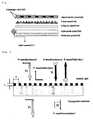
- Fig. 3shows a stacking sequence of an LCD panel using a wire grid polarization film in accordance with one embodiment of the present invention.
- the LCD panelcomprises a light source 101, a reflective plate 102, a light guide plate 103, a diffusion plate 104, a prism sheet 105, a wire grid polarization film 300, and a liquid crystal panel 106.
- Fig. 3schematically shows a stacked position of a wire grid polarization film 300 according to this embodiment.
- the reflective plate 102is positioned at the lowermost portion of the LCD panel, and the light guide plate 103, the diffusion plate 104 and the prism sheet 105 are sequentially stacked on the reflective plate 102.
- the light source 101is positioned at one side of the light guide plate 103.
- the wire grid polarization film 300 of the present invention, and the liquid crystal panel 106are sequentially stacked on the prism sheet 105.
- the wire grid polarization film 300is positioned between a conventional backlight unit and the LCD panel.
- the prism sheet 105 of Fig. 3is selectively used, and may be positioned on the wire grid polarization film 300. That is, it is possible to constitute an optical film in various shapes. A portion of polarized light reflected by the wire grid polarization film 300 is changed in direction while being reflected back again through the backlight unit positioned below the LCD panel, and then passes through the wire grid polarization film 300, thereby increasing brightness.
- Fig. 4is a perspective view illustrating a grid structure of the wire grid polarization film according to the embodiment.
- the wire grid polarization filmcomprises a polymer substrate 301, a polymer thin film 302 stacked on the polymer substrate 301, and a metal layer 303 stacked on the polymer thin film 302.
- Fig. 4schematically shows a method for forming the grid structure according to this embodiment.
- the wire grid polarization filmcomprises a polymer plastic film substrate 301 having excellent mechanical properties and a good optical transmissivity, and a grid structure layer, which allows easy formation and has a good optical transmissivity, on the polymer plastic film 301.
- the grid structure layercomprises a grid structure composed of the polymer thin film 302, and the metallic layer 303 formed on one side of each ridge of the grid structure.
- the grid structuremust have a grid period of 220 nm in order to provide a good polarization efficiency in an overall wavelength band of visible light. The shorter the grid period is, the higher a polarization extinction ratio is.
- the polymer plastic film substrate 301is formed of a polymer material such as PET and the like.
- the polymer thin film 302 having the grid structure formed thereonis formed of, for example, acryl, polycarbonate or polyurethane.
- the metallic layer 303is formed of metal, such as aluminum, silver and the like, which has a good reflectance in an overall wavelength band of visible light.
- each ridge of a grid formed on the polymer thin filmmay have not only a triangular shape as shown in Fig. 4, but also a rectangular shape, a trapezoid shape, a semicircular shape, a semi-elliptical shape, etc.
- the metallic layeris deposited only on one side of each figure constituting each ridge of the grid.
- the metallic layeris deposited on an upper face and a portion of one side among three faces protruding to an upper portion.
- the shape of the metallic layeris changed according to a deposition angle of the metallic layer.
- the metallic layer 303has an elongated shape formed in one dimension on one side of each ridge of the grid, or in some cases, on the upper end of each ridge thereof in a direction of the grid.
- the polarizerhas a good transmissivity, the polarization extinction ratio thereof deteriorates.
- the transmissivity and the polarization extinction ratioare determined according to utility of the polarizer, and if the metallic layer is thickened, the transmissivity is enhanced whereas the polarization extinction ratio deteriorates. That is, the polarization extinction ratio varies significantly according to change of the thickness and width of the metallic layer, and the wire grid polarization film is preferably manufactured in consideration of the transmissivity.
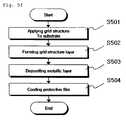
- Figs. 5a to 5eshow a method for manufacturing a wire grid polarization film in accordance with one embodiment of the present invention.
- a plastic film substrate 301is prepared (Fig. 5a), and then a polymer thin film 302 is deposited thereon (Fig. 5b) (S501).
- the thin filmis composed of a heat-curable or UV-curable polymer thin film, and allows for the formation of fine patterns.
- a grid structure layeris formed on the polymer thin film 302 using a mold having a fine pattern formed thereon (Fig. 5c) (S502). Formation of the grid structure is performed differently according to the properties of the polymer thin film 302.
- the formation of the grid structureis performed at an increased temperature, and for the UV-curable polymer thin film, the formation of the grid structure is performed by illuminating with ultraviolet rays and applying a suitable pressure. Then, a metallic layer 303 is deposited on one side of each ridge of the grid structure in a slanted direction (Fig. 5d) (S503). The metallic layer 303 is deposited on the grid structure by spraying metallic powder in a predetermined direction with respect to the polymer thin film 302. Finally, a protective film 304 is coated on the grid structure and the metallic layer (Fig. 5e) (S504). The protective film 304 serves to prevent corrosion of aluminum, and damage of surface when using the film.
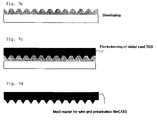
- Fig. 6shows an apparatus for manufacturing the wire grid polarizers in mass production according to one embodiment of the invention.
- the apparatus for manufacturing the wire grid polarization film in mass productioncomprises a grid forming part 601, a metal deposition part 602, and a protective film coating part 604.
- Fig. 6schematically shows a method of continuously producing the wire grid polarizers using a mold roller 600 of the apparatus according to this embodiment.
- a grid patternis formed on the substrate by the mold roller 600 of the grid forming part 601. Then, the substrate having the grid pattern formed thereon is conveyed to the metal deposition part 603 by means of a roller 602b. At the metal deposition part 603, a metallic layer is formed on one side of each ridge of the grid pattern. Then, the substrate having the metallic layer formed thereon is conveyed to the protective film coating part 604 where a protective film is formed on the uppermost layer.
- a roll-to-roll type processis adopted in order to allow high speed production of the wire grid polarizers.
- Fig. 6the roll-to-roll type process of manufacturing the wire grid polarizers is shown.
- the mold of the inventionmay be made of any of various materials, such as metal, polymer plastic, silicone, quartz, and the like.
- the moldis preferably made of nickel or polymer plastic.
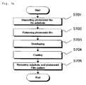
- the mold rollercan be manufactured via various lithography processes, and in particular, a laser interference lithography process is most efficient.
- Figs. 7a to 7eare views illustrating a method for manufacturing the mold roller of Fig. 6 in accordance with one embodiment of the present invention.
- Figs. 7a to 7eschematically show the laser interference lithography process for manufacturing the mold master used for the wire grid polarization film according to this embodiment.
- the laser interference lithography processcomprises the steps of applying a photoresist film 702 on a substrate 701 (S701), and patterning the photoresist film 702 by forming interference fringes thereon via illumination by laser in two directions (Fig. 7a) (S702). At this time, a minimum period of the pattern to be formed is half of a wavelength of the laser. After exposing and developing the photoresist film (Fig. 7b) (S703), electroforming of nickel is performed to form a nickel coat 703 on the photoresist pattern 702 (Fig. 7c) (S704). Finally, a nickel mold master 700 is completed by separating the substrate 701 and the photoresist pattern 702 (Fig. 7d) (S705). The nickel mold master 700 may be directly employed for forming a pattern on the polymer thin film. Alternatively, after imprinting the pattern of the nickel mold master 700 on a separate plastic film, the separate plastic film is used as a mold.
- the present inventionenables mass production of large sized wire grid polarization films at high speed, allowing easy application of the wire grid polarization films for enhancement in brightness of a liquid crystal display and other fields.
Landscapes
- Physics & Mathematics (AREA)
- General Physics & Mathematics (AREA)
- Optics & Photonics (AREA)
- Nonlinear Science (AREA)
- Mathematical Physics (AREA)
- Chemical & Material Sciences (AREA)
- Crystallography & Structural Chemistry (AREA)
- Polarising Elements (AREA)
- Liquid Crystal (AREA)
Abstract
Description
- The present invention relates to a wire grid polarization film, and a method for manufacturing a mold for forming a grid of the same.
- Generally, a liquid crystal display (LCD) is a flat panel display which is used in a wide variety of applications including mobile phones, notebook computers, monitors, televisions, etc. The LCD is a device for transmitting or shielding light by changing an arrangement of liquid crystals via application of electric signals to respective pixels in a liquid crystal panel positioned between two polarizing plates. Thus, a separate light source is required to operate the LCD, and the LCD can be classified into a reflective type LCD and a transmissive type LCD according to a method of using the light source. The reflective type LCD employs an external light source such as sunlight or a room lamp, and is configured such that light from the external light source is incident to a front side of an LCD panel, and is reflected by a reflector positioned at a rear side of the LCD panel to a viewer. The transmissive type LCD employs a backlight unit (BLU) as the light source, and is configured such that light uniformly emitted from the BLU at a rear side of the LCD panel passes through the rear side of the LCD panel to a viewer.
- Fig. 1 shows the structure of the transmissive type LCD. An LCD which employs both an external light source and a backlight unit is referred to as a trans-reflective type LCD. Generally, the BLU comprises a light source such as fluorescent lamps and LEDs, a
light guide panel 103 to guide light to an entire surface on a front side of an LCD panel,diffusion films 104, aprism sheet 105, and the like. With this structure, a substantial portion of light emitted from the light source is lost while passing through the BLU. In addition, since the diffusion films disposed on the front and rear sides of the LCD panel are absorbent, they absorb 50 % of light directed towards the LCD panel. Thus, light reaching the viewer of the LCD is 10 % or less of the light emitted from the light source. This means that the LCD has a low utilization efficiency of light. In this regard, enhancement in utilization efficiency of light enables an increase in utilization period of a battery for portable devices, and a reduction of power consumption in a large sized LCD TV. - As technology for increasing brightness of the LCD by enhancing the utilization efficiency of light of the LCD, a dual brightness enhancement film (DBEF) available from Minnesota Mining & Manufacturing Co. in U.S.A. has been evaluated as a unique means. The DBEF is a multilayer polymeric thin film type reflective polarizing plate. For the case of the transmissive type LCD, the DBEF is positioned between the BLU and the LCD panel to increase brightness to a degree of 60 %. In other words, a specific polarized light reflected by the reflective polarizing plate is changed in polarization while being reflected again through the BLU positioned at a lower portion, and then some of the polarized light passing through the polarization plate, i.e. the DBEF, is used for increasing the brightness. However, since the DBEF is manufactured to form a multilayer film by crossing an optically anisotropic polymer film and an optically isotropic polymer film, it is expensive, and made via a complicated manufacturing process.
- As another type of reflective polarizing plate, there is a wire grid polarizer. It has been well known in the art that metal wires arranged in parallel selectively transmit or reflect an electromagnetic wave according to components of polarized light. If an arranging period of the metal wires is shorter than half of a wavelength of an incident electromagnetic wave, a component of the polarized light in parallel with the metal wires, i.e., s-wave, is reflected, whereas a component of the polarized light vertical to the metal wires, i.e., p-wave, is transmitted. By using this phenomenon, it is possible to manufacture a planar polarizer which has excellent polarization efficiency, high transmissivity, and a wide view angle.
- Fig. 2 shows a wire grid polarizer.
- Performance of the wire grid polarization film can be represented by a polarization extinction ratio and transmissivity. In order to have a higher polarization extinction ratio, the wire grid polarization film must satisfy a prerequisite that a period of a metal grid is significantly shorter than a wavelength of an incident light. However, since a shorter period of the metal grid complicates a process of manufacturing the wire grid polarizer, the wire grid polarization film has been used mainly in the range of microwaves or infrared radiation. However, as fine patterns can be formed via development of a semiconductor manufacturing apparatus and an exposing technique, it becomes possible to manufacture a wire grid polarizer operating in the wavelength band of visible light.
- The range of the visible light generally refers to a wavelength band from 400 to 700 nm. Accordingly, for the wire grid polarization film operating in the wavelength band of visible light, the period of the metal grid must be at least 200 nm or less in order to achieve a polarization property to some extent. Furthermore, in order to exhibit excellent performance or the same performance as that of a conventional polarizer, it is desirable that the metallic grids have a period in the range of 100's nm.
- The conventional wire grid polarization film operating in the wavelength band of visible light is used on a transparent glass substrate, and is manufactured by a semiconductor process such as dry etching. Thus, the conventional wire grid polarization film has a restriction in an increase in area thereof so as to be available for a medium or large sized display of 10 inches or more, and is very expensive. In addition, due to use of the glass substrate, the conventional wire grid polarization film has problems of heavy weight and large thickness even if the wire grid polarization film is manufactured to have a large area.
- The present invention has been made to solve the above problems, and it is an object of the present invention to provide a method for manufacturing wire grid polarizers of a large area in mass production at low costs, and a mold for the wire grid polarization film for mass production.
- In accordance with one aspect of the present invention, the above and other objects can be accomplished by the provision of a wire grid polarization film, comprising: a substrate; a grid structure layer stacked on the substrate; and at least one metallic layer formed on one side of the grid structure layer.
- Preferably, the substrate is composed of a polymer plastic substrate having an excellent optical transmissivity, and the polymer plastic substrate is made of polyethylenterephtalate (PET).
- Preferably, the grid structure layer is formed using a heat-curable or UV-curable polymer thin film allowing easy molding, and the polymer thin film is made of at least one material selected from acryl, polycarbonate and polyurethane.
- Preferably, the grid structure layer has a grid period of 220 nm or less.
- Preferably, each ridge of the,grid structure layer has a cross-section selected from a triangular shape, a rectangular shape, a trapezoid shape, a semicircular shape, and a semi-elliptical shape.
- Preferably, the at least one metallic layer comprises a plurality of metallic layers formed in a longitudinal direction of the substrate.
- Preferably, the wire grid polarization film further comprises a protective film coated on an upper surface of the metallic layer and an upper surface of the grid structure layer where the metallic layer is not formed thereon.
- In accordance with another aspect of the present invention, an apparatus for manufacturing a wire grid polarization film is provided, comprising: a grid forming part to form a grid pattern on a substrate; a metal deposition part to deposit a metallic layer on one side of the grid pattern; and a protective film coating part to coat a protective film on an upper surface of the metallic layer and an upper surface of the grid pattern where the metallic layer is not formed thereon.
- Preferably, the grid forming part comprises a mold roller having the same cross-section as that of the grid pattern to be manufactured.
- In accordance with further another aspect of the present invention, a method for manufacturing a wire grid polarization film is provided, comprising the steps of: preparing a substrate; applying a grid structure layer to an upper surface the substrate; forming a grid pattern on the grid structure layer; and depositing a metal layer on the grid pattern.
- Preferably, the method further comprises coating a protective film on the grid pattern.
- Preferably, the metal layer is deposited only on one side of each ridge of the grid pattern.
- Preferably, the grid pattern is formed by a mold roller.
- In accordance with yet aspect of the present invention, a method for manufacturing a mold for forming a grid of a wire grid polarization film is provided, comprising the steps of: applying a photoresist film on a substrate, followed by patterning the photoresist film using interference fringes via laser; developing the photoresist film, followed by stacking a material for forming a grid pattern of the wire grid polarization film on the photoresist film; and removing the substrate and the photoresist film.
- Preferably, the material is at least one selected from metal, polymer plastic, silicone, and quartz.
- The foregoing and other objects and features of the present invention will be more clearly understood from the following detailed description taken in conjunction with the accompanying drawings, in which:
- Fig. 1 shows a general structure of an LCD panel;
- Fig. 2 shows the structure and a principle of a wire grid polarizer;
- Fig. 3 shows a stacked position of a wire grid polarization film for enhancing brightness of an LCD in accordance with one embodiment of the present invention;
- Fig. 4 shows the structure of a wire grid polarization film in accordance with the embodiment;
- Figs. 5a to 5e show a method for manufacturing a wire grid polarization film in accordance with one embodiment of the present invention;
- Fig. 6 shows an apparatus for manufacturing a wire grid polarization films in mass production via a roll-to-roll process in accordance with one embodiment of the present invention; and
- Figs. 7a to 7e are a method for manufacturing a mold master via an interference lithography process in accordance with one embodiment of the present invention.
- Preferred embodiments of the present invention will be described in detail with reference to the accompanying drawings, in which like components are denoted by the same reference numerals. Well-known functions and constructions which can make the subject matter of the present invention unclear will be omitted hereinafter.
- Fig. 3 shows a stacking sequence of an LCD panel using a wire grid polarization film in accordance with one embodiment of the present invention.
- In this embodiment, the LCD panel comprises a
light source 101, areflective plate 102, alight guide plate 103, adiffusion plate 104, aprism sheet 105, a wiregrid polarization film 300, and aliquid crystal panel 106. - Fig. 3 schematically shows a stacked position of a wire
grid polarization film 300 according to this embodiment. - Referring to Fig. 3, the
reflective plate 102 is positioned at the lowermost portion of the LCD panel, and thelight guide plate 103, thediffusion plate 104 and theprism sheet 105 are sequentially stacked on thereflective plate 102. Thelight source 101 is positioned at one side of thelight guide plate 103. The wiregrid polarization film 300 of the present invention, and theliquid crystal panel 106 are sequentially stacked on theprism sheet 105. - The wire
grid polarization film 300 is positioned between a conventional backlight unit and the LCD panel. Theprism sheet 105 of Fig. 3 is selectively used, and may be positioned on the wiregrid polarization film 300. That is, it is possible to constitute an optical film in various shapes. A portion of polarized light reflected by the wiregrid polarization film 300 is changed in direction while being reflected back again through the backlight unit positioned below the LCD panel, and then passes through the wiregrid polarization film 300, thereby increasing brightness. - Fig. 4 is a perspective view illustrating a grid structure of the wire grid polarization film according to the embodiment.
- According to the embodiment, the wire grid polarization film comprises a
polymer substrate 301, a polymerthin film 302 stacked on thepolymer substrate 301, and ametal layer 303 stacked on the polymerthin film 302. - Fig. 4 schematically shows a method for forming the grid structure according to this embodiment.
- Referring to Fig. 4, the wire grid polarization film comprises a polymer
plastic film substrate 301 having excellent mechanical properties and a good optical transmissivity, and a grid structure layer, which allows easy formation and has a good optical transmissivity, on thepolymer plastic film 301. The grid structure layer comprises a grid structure composed of the polymerthin film 302, and themetallic layer 303 formed on one side of each ridge of the grid structure. The grid structure must have a grid period of 220 nm in order to provide a good polarization efficiency in an overall wavelength band of visible light. The shorter the grid period is, the higher a polarization extinction ratio is. - Preferably, the polymer
plastic film substrate 301 is formed of a polymer material such as PET and the like. The polymerthin film 302 having the grid structure formed thereon is formed of, for example, acryl, polycarbonate or polyurethane. Preferably, themetallic layer 303 is formed of metal, such as aluminum, silver and the like, which has a good reflectance in an overall wavelength band of visible light. - As for a cross-section of each ridge of a grid formed on the polymer thin film, it may have not only a triangular shape as shown in Fig. 4, but also a rectangular shape, a trapezoid shape, a semicircular shape, a semi-elliptical shape, etc. In this regard, an important point is that the metallic layer is deposited only on one side of each figure constituting each ridge of the grid. In other words, for the case of the rectangular or trapezoid shape, the metallic layer is deposited on an upper face and a portion of one side among three faces protruding to an upper portion. The shape of the metallic layer is changed according to a deposition angle of the metallic layer. Here, an important point is that metal is prevented from being deposited on other portions of the one side and a trench portion (a depressed portion) of each ridge of the grid. Thus, when depositing the metallic layer, a method of spraying metal at about 45 degrees with respect to the grid after forming the grid, which will be described in detail below, is used.
- With this method, the
metallic layer 303 has an elongated shape formed in one dimension on one side of each ridge of the grid, or in some cases, on the upper end of each ridge thereof in a direction of the grid. Generally, if the polarizer has a good transmissivity, the polarization extinction ratio thereof deteriorates. The transmissivity and the polarization extinction ratio are determined according to utility of the polarizer, and if the metallic layer is thickened, the transmissivity is enhanced whereas the polarization extinction ratio deteriorates. That is, the polarization extinction ratio varies significantly according to change of the thickness and width of the metallic layer, and the wire grid polarization film is preferably manufactured in consideration of the transmissivity. - Figs. 5a to 5e show a method for manufacturing a wire grid polarization film in accordance with one embodiment of the present invention.
- Referring to Figs. 5a and 5b, first, a
plastic film substrate 301 is prepared (Fig. 5a), and then a polymerthin film 302 is deposited thereon (Fig. 5b) (S501). Preferably, the thin film is composed of a heat-curable or UV-curable polymer thin film, and allows for the formation of fine patterns. Next, a grid structure layer is formed on the polymerthin film 302 using a mold having a fine pattern formed thereon (Fig. 5c) (S502). Formation of the grid structure is performed differently according to the properties of the polymerthin film 302. Specifically, for the heat-curable polymer thin film, the formation of the grid structure is performed at an increased temperature, and for the UV-curable polymer thin film, the formation of the grid structure is performed by illuminating with ultraviolet rays and applying a suitable pressure. Then, ametallic layer 303 is deposited on one side of each ridge of the grid structure in a slanted direction (Fig. 5d) (S503). Themetallic layer 303 is deposited on the grid structure by spraying metallic powder in a predetermined direction with respect to the polymerthin film 302. Finally, a protective film 304 is coated on the grid structure and the metallic layer (Fig. 5e) (S504). The protective film 304 serves to prevent corrosion of aluminum, and damage of surface when using the film. - Fig. 6 shows an apparatus for manufacturing the wire grid polarizers in mass production according to one embodiment of the invention.
- In this embodiment, the apparatus for manufacturing the wire grid polarization film in mass production comprises a
grid forming part 601, ametal deposition part 602, and a protectivefilm coating part 604. - Fig. 6 schematically shows a method of continuously producing the wire grid polarizers using a
mold roller 600 of the apparatus according to this embodiment. - Referring to Fig. 6, while a substrate is conveyed by means of a roller 602a, a grid pattern is formed on the substrate by the
mold roller 600 of thegrid forming part 601. Then, the substrate having the grid pattern formed thereon is conveyed to themetal deposition part 603 by means of a roller 602b. At themetal deposition part 603, a metallic layer is formed on one side of each ridge of the grid pattern. Then, the substrate having the metallic layer formed thereon is conveyed to the protectivefilm coating part 604 where a protective film is formed on the uppermost layer. - Although the respective steps of the process can be performed using separate plastic substrates by separate apparatuses, a roll-to-roll type process is adopted in order to allow high speed production of the wire grid polarizers. In Fig. 6, the roll-to-roll type process of manufacturing the wire grid polarizers is shown.
- The mold of the invention may be made of any of various materials, such as metal, polymer plastic, silicone, quartz, and the like. In order to allow production of a large area polarizer, the mold is preferably made of nickel or polymer plastic. The mold roller can be manufactured via various lithography processes, and in particular, a laser interference lithography process is most efficient.
- Figs. 7a to 7e are views illustrating a method for manufacturing the mold roller of Fig. 6 in accordance with one embodiment of the present invention.
- Figs. 7a to 7e schematically show the laser interference lithography process for manufacturing the mold master used for the wire grid polarization film according to this embodiment.
- Referring to Figs. 7a to 7e, the laser interference lithography process comprises the steps of applying a
photoresist film 702 on a substrate 701 (S701), and patterning thephotoresist film 702 by forming interference fringes thereon via illumination by laser in two directions (Fig. 7a) (S702). At this time, a minimum period of the pattern to be formed is half of a wavelength of the laser. After exposing and developing the photoresist film (Fig. 7b) (S703), electroforming of nickel is performed to form anickel coat 703 on the photoresist pattern 702 (Fig. 7c) (S704). Finally, anickel mold master 700 is completed by separating thesubstrate 701 and the photoresist pattern 702 (Fig. 7d) (S705). Thenickel mold master 700 may be directly employed for forming a pattern on the polymer thin film. Alternatively, after imprinting the pattern of thenickel mold master 700 on a separate plastic film, the separate plastic film is used as a mold. - As apparent from the above description, the present invention enables mass production of large sized wire grid polarization films at high speed, allowing easy application of the wire grid polarization films for enhancement in brightness of a liquid crystal display and other fields.
- It should be understood that the embodiments and the accompanying drawings have been described for illustrative purposes and the present invention is limited by the following claims. Further, those skilled in the art will appreciate that various modifications, additions and substitutions are allowed without departing from the scope and spirit of the invention as set forth in the accompanying claims.
Claims (18)
- A wire grid polarization film, comprising: a substrate; a grid structure layer stacked on the substrate; and at least one metallic layer formed on one side of the grid structure layer.
- The wire grid polarization film according to claim 1, wherein the substrate is composed of a polymer plastic substrate having an excellent optical transmissivity.
- The wire grid polarization film according to claim 2, wherein the polymer plastic substrate is made of polyethylenterephtalate (PET).
- The wire grid polarization film according to claim 1, wherein the grid structure layer is formed using a heat-curable or UV-curable polymer thin film allowing easy molding.
- The wire grid polarization film according to claim 4, wherein the polymer thin film is made of at least one material selected from acryl, polycarbonate, and polyurethane.
- The wire grid polarization film according to claim 1, wherein the grid structure layer has a grid period of 220 nm or less.
- The wire grid polarization film according to claim 1, wherein each ridge of the grid structure layer has a cross-section selected from a triangular shape, a rectangular shape, a trapezoid shape, a semicircular shape, and a semi-elliptical shape.
- The wire grid polarization film according to claim 1, wherein the at least one metallic layer comprises a plurality of metallic layers formed in a longitudinal direction of the substrate.
- The wire grid polarization film according to claim 1, further comprising: a protective film coated on an upper surface of the metallic layer and an upper surface of the grid structure layer where the metallic layer is not formed thereon
- A liquid crystal display comprising a wire grid polarization film according to claim 1.
- An apparatus for manufacturing a wire grid polarization film, comprising: a grid forming part to form a grid pattern on a substrate; a metal deposition part to deposit a metallic layer on one side of the grid pattern; and a protective film coating part to coat a protective film on an upper surface of the metallic layer and an upper surface of the grid pattern where the metallic layer is not formed thereon.
- The apparatus according to claim 11, wherein the grid forming part comprises a mold roller having the same cross-section as that of the grid pattern to be manufactured.
- A method for manufacturing a wire grid polarization film, comprising the steps of: preparing a substrate; applying a grid structure layer to an upper surface the substrate; forming a grid pattern on the grid structure layer; and depositing a metal layer on the grid pattern.
- The method according to claim 13, further comprising: coating a protective film on the grid pattern.
- The method according to claim 13, wherein the metal layer is deposited only on one side of each ridge of the grid pattern.
- The method according to claim 13, wherein the grid pattern is formed by a mold roller.
- A method for manufacturing a mold for forming a grid of a wire grid polarization film, comprising the steps of: applying a photoresist film on a substrate, followed by patterning the photoresist film using interference fringes via laser; developing the photoresist film, followed by stacking a material for forming a grid pattern of the wire grid polarization film on the photoresist film; and removing the substrate and the photoresist film.
- The method according to claim 17, wherein the material is at least one selected from metal, polymer plastic, silicone, and quartz.
Applications Claiming Priority (1)
| Application Number | Priority Date | Filing Date | Title |
|---|---|---|---|
| KR1020050005123AKR100656999B1 (en) | 2005-01-19 | 2005-01-19 | Method of manufacturing mold for manufacturing lattice of line lattice polarizing film and line lattice polarizing film |
Publications (2)
| Publication Number | Publication Date |
|---|---|
| EP1684099A2true EP1684099A2 (en) | 2006-07-26 |
| EP1684099A3 EP1684099A3 (en) | 2006-08-02 |
Family
ID=35929780
Family Applications (1)
| Application Number | Title | Priority Date | Filing Date |
|---|---|---|---|
| EP20060001118WithdrawnEP1684099A3 (en) | 2005-01-19 | 2006-01-19 | Wire grid polarization film, method for manufacturing wire grid polarization film, liquid crystal display using wire grid polarization film, and method for manufacturing mold for forming wire grids thereof |
Country Status (5)
| Country | Link |
|---|---|
| US (1) | US20060159958A1 (en) |
| EP (1) | EP1684099A3 (en) |
| JP (1) | JP2006201782A (en) |
| KR (1) | KR100656999B1 (en) |
| CN (1) | CN1866062A (en) |
Cited By (4)
| Publication number | Priority date | Publication date | Assignee | Title |
|---|---|---|---|---|
| WO2017151291A1 (en)* | 2016-03-04 | 2017-09-08 | Applied Materials, Inc. | Wire grid polarizer manufacturing method |
| CN107708744A (en)* | 2015-07-08 | 2018-02-16 | 卡丽·马特兹 | Systems for storing and sterilizing complex devices |
| WO2022231825A1 (en)* | 2021-04-29 | 2022-11-03 | Meta Platforms Technologies, Llc | High surface quality optical film |
| US11592740B2 (en) | 2017-05-16 | 2023-02-28 | Applied Materials, Inc. | Wire grid polarizer manufacturing methods using frequency doubling interference lithography |
Families Citing this family (48)
| Publication number | Priority date | Publication date | Assignee | Title |
|---|---|---|---|---|
| JP2008522226A (en) | 2004-11-30 | 2008-06-26 | アグーラ テクノロジーズ インコーポレイテッド | Application and fabrication technology of large-scale wire grid polarizer |
| US7351346B2 (en)* | 2004-11-30 | 2008-04-01 | Agoura Technologies, Inc. | Non-photolithographic method for forming a wire grid polarizer for optical and infrared wavelengths |
| KR20070074787A (en)* | 2005-06-13 | 2007-07-18 | 삼성전자주식회사 | Gray voltage generator and liquid crystal display |
| US20070217008A1 (en)* | 2006-03-17 | 2007-09-20 | Wang Jian J | Polarizer films and methods of making the same |
| KR20090006066A (en)* | 2006-04-07 | 2009-01-14 | 아사히 가라스 가부시키가이샤 | Wire grid polarizer and its manufacturing method |
| WO2008026374A1 (en)* | 2006-08-29 | 2008-03-06 | Sharp Kabushiki Kaisha | Polarizing plate, polarizing plate manufacturing method, display panel and display element |
| WO2008042658A2 (en)* | 2006-09-29 | 2008-04-10 | Agoura Technologies, Inc. | Display having integrated functions in one or more layers |
| US20080129930A1 (en)* | 2006-12-01 | 2008-06-05 | Agoura Technologies | Reflective polarizer configuration for liquid crystal displays |
| KR100793176B1 (en) | 2007-02-23 | 2008-01-14 | (주)나노비전 | LCD and its manufacturing method |
| US8027086B2 (en)* | 2007-04-10 | 2011-09-27 | The Regents Of The University Of Michigan | Roll to roll nanoimprint lithography |
| US7821110B2 (en)* | 2007-05-11 | 2010-10-26 | International Business Machines Corporation | Circuit structures and methods with BEOL layer(s) configured to block electromagnetic interference |
| JP5010527B2 (en)* | 2007-06-04 | 2012-08-29 | 住友化学株式会社 | Light guide plate unit, surface light source device, and liquid crystal display device |
| US20100136233A1 (en)* | 2007-08-02 | 2010-06-03 | Little Michael J | Oblique vacuum deposition for roll-roll coating of wire grid polarizer lines oriented in a down-web direction |
| WO2009018107A1 (en)* | 2007-08-02 | 2009-02-05 | Agoura Technologies, Inc. | Nanoembossed shapes and fabrication methods of wire grid polarizers |
| JP2009053574A (en)* | 2007-08-29 | 2009-03-12 | Nippon Zeon Co Ltd | Polarized illumination device |
| US20090195729A1 (en)* | 2007-09-25 | 2009-08-06 | Agoura Technologies, Inc. | Display having integrated functions in one or more layers |
| TW200928462A (en)* | 2007-12-28 | 2009-07-01 | Ind Tech Res Inst | Wire grid polarizer and method of fabrication |
| JP4903735B2 (en)* | 2008-03-03 | 2012-03-28 | 三菱電機株式会社 | Backlight device |
| JP4972015B2 (en) | 2008-03-10 | 2012-07-11 | 富士フイルム株式会社 | Mold processing method and manufacturing method |
| JP5227692B2 (en)* | 2008-08-05 | 2013-07-03 | 旭化成イーマテリアルズ株式会社 | Manufacturing method of wire grid polarizing plate |
| US8138563B2 (en) | 2008-08-08 | 2012-03-20 | International Business Machines Corporation | Circuit structures and methods with BEOL layers configured to block electromagnetic edge interference |
| KR101610376B1 (en)* | 2009-04-10 | 2016-04-08 | 엘지이노텍 주식회사 | A wire grid polarizer, liquid crystal display including the same and method of manufacturing the wire grid polarizer |
| JP5583363B2 (en)* | 2009-06-23 | 2014-09-03 | 旭化成イーマテリアルズ株式会社 | Wire grid polarizing plate and manufacturing method thereof |
| KR101064424B1 (en)* | 2009-10-01 | 2011-09-14 | 김장규 | Encapsulation film for organic light emitting diode and manufacturing method thereof |
| CN102713697A (en)* | 2009-10-08 | 2012-10-03 | 旭硝子株式会社 | Wire grid type polarizer and method for manufacturing same |
| US20110244187A1 (en)* | 2010-04-06 | 2011-10-06 | Modilis Holdings Llc | Internal Cavity Optics |
| US8611007B2 (en) | 2010-09-21 | 2013-12-17 | Moxtek, Inc. | Fine pitch wire grid polarizer |
| KR20120075877A (en)* | 2010-12-29 | 2012-07-09 | 삼성전자주식회사 | Liquid crystal display panel and apparautus thereof |
| EP2947506A4 (en) | 2013-01-16 | 2016-07-13 | Sharp Kk | Mirror display, half mirror plate, and electronic device |
| CN104133263A (en)* | 2013-05-02 | 2014-11-05 | 罗伯特·彼得科维奇 | Preparation method of polarizer |
| CN104133264A (en)* | 2013-05-02 | 2014-11-05 | 罗伯特·彼得科维奇 | Method for preparing polarizer |
| WO2015019858A1 (en) | 2013-08-05 | 2015-02-12 | シャープ株式会社 | Mirror display, half mirror plate, and electronic device |
| WO2015141350A1 (en) | 2014-03-19 | 2015-09-24 | シャープ株式会社 | Mirror display and electronic device |
| CN106461958B (en) | 2014-06-05 | 2019-01-01 | 夏普株式会社 | Mirror display system |
| US10254455B2 (en) | 2014-06-05 | 2019-04-09 | Sharp Kabushiki Kaisha | Mirror display and mirror display unit |
| EP3161857B1 (en) | 2014-06-26 | 2021-09-08 | Wostec, Inc. | Method of forming a wavelike hard nanomask on a topographic feature |
| CN104516164B (en) | 2015-01-05 | 2018-03-09 | 京东方科技集团股份有限公司 | A kind of display base plate and preparation method thereof and display device |
| KR20160143443A (en)* | 2015-06-05 | 2016-12-14 | 코오롱인더스트리 주식회사 | Wire Grid Polarizer And Liquid Crystal Display Device Including The Same |
| CN105700058A (en)* | 2016-04-05 | 2016-06-22 | 武汉华星光电技术有限公司 | Metal wire grating brightness enhance film for display backlight and preparation method for metal wire grating brightness enhance film |
| US10921638B2 (en) | 2016-07-06 | 2021-02-16 | Sharp Kabushiki Kaisha | Display device, electronic apparatus, semi-transmissive reflection plate, and electrical apparatus |
| US10672427B2 (en) | 2016-11-18 | 2020-06-02 | Wostec, Inc. | Optical memory devices using a silicon wire grid polarizer and methods of making and using |
| WO2018156042A1 (en) | 2017-02-27 | 2018-08-30 | Wostec, Inc. | Nanowire grid polarizer on a curved surface and methods of making and using |
| CN107121719B (en)* | 2017-07-03 | 2019-06-25 | 京东方科技集团股份有限公司 | A kind of preparation method of wire grid polarizer, display device and wire grid polarizer |
| WO2019066674A1 (en)* | 2017-09-27 | 2019-04-04 | Wostec, Inc. | Optical devices with nanowire grid polarizer on a curved surface and methods of making and using |
| US11226483B2 (en)* | 2018-06-07 | 2022-01-18 | Facebook Technologies, Llc | Reverse-order crossed pancake lens with a shaped polarizer |
| CN109212898A (en)* | 2018-11-05 | 2019-01-15 | 京东方科技集团股份有限公司 | A kind of nano-imprint stamp and preparation method thereof |
| JP2022098931A (en) | 2020-12-22 | 2022-07-04 | シャープ株式会社 | Liquid crystal display device |
| JP7488307B2 (en) | 2022-10-12 | 2024-05-21 | シャープディスプレイテクノロジー株式会社 | Display device |
Family Cites Families (6)
| Publication number | Priority date | Publication date | Assignee | Title |
|---|---|---|---|---|
| US3291871A (en)* | 1962-11-13 | 1966-12-13 | Little Inc A | Method of forming fine wire grids |
| CA2019046C (en)* | 1989-06-16 | 1998-05-12 | Satoshi Okazaki | Method of printing fine patterns |
| EP1003078A3 (en)* | 1998-11-17 | 2001-11-07 | Corning Incorporated | Replicating a nanoscale pattern |
| US8054416B2 (en)* | 2000-08-15 | 2011-11-08 | Reflexite Corporation | Light polarizer |
| GB0106050D0 (en)* | 2001-03-12 | 2001-05-02 | Suisse Electronique Microtech | Polarisers and mass-production method and apparatus for polarisers |
| KR20040092139A (en)* | 2003-04-25 | 2004-11-03 | 엘지전자 주식회사 | grid fabrication method |
- 2005
- 2005-01-19KRKR1020050005123Apatent/KR100656999B1/ennot_activeExpired - Fee Related
- 2006
- 2006-01-18JPJP2006010529Apatent/JP2006201782A/ennot_activeWithdrawn
- 2006-01-18USUS11/335,302patent/US20060159958A1/ennot_activeAbandoned
- 2006-01-19EPEP20060001118patent/EP1684099A3/ennot_activeWithdrawn
- 2006-01-19CNCNA2006100059087Apatent/CN1866062A/enactivePending
Non-Patent Citations (1)
| Title |
|---|
| BRUNOTTE M; MORF R; SCHLERETH K -H; BOTTNER H: "Ultra-thin lamellar gratings as solar selective coatings", PROCEEDINGS OF THE SPIE - THE INTERNATIONAL SOCIETY FOR OPTICAL ENGINEERING 1990 USA, vol. 1272, 1990, pages 2 - 11, Retrieved from the Internet <URL:http://spiedl.aip.org/getabs/servlet/GetabsServlet?prog=normal&id=PSISDG001272000001000002000001&idtype=cvips&gifs=Yes>* |
Cited By (5)
| Publication number | Priority date | Publication date | Assignee | Title |
|---|---|---|---|---|
| CN107708744A (en)* | 2015-07-08 | 2018-02-16 | 卡丽·马特兹 | Systems for storing and sterilizing complex devices |
| WO2017151291A1 (en)* | 2016-03-04 | 2017-09-08 | Applied Materials, Inc. | Wire grid polarizer manufacturing method |
| US10983389B2 (en) | 2016-03-04 | 2021-04-20 | Applied Materials, Inc. | Wire grid polarizer manufacturing method |
| US11592740B2 (en) | 2017-05-16 | 2023-02-28 | Applied Materials, Inc. | Wire grid polarizer manufacturing methods using frequency doubling interference lithography |
| WO2022231825A1 (en)* | 2021-04-29 | 2022-11-03 | Meta Platforms Technologies, Llc | High surface quality optical film |
Also Published As
| Publication number | Publication date |
|---|---|
| JP2006201782A (en) | 2006-08-03 |
| CN1866062A (en) | 2006-11-22 |
| EP1684099A3 (en) | 2006-08-02 |
| US20060159958A1 (en) | 2006-07-20 |
| KR100656999B1 (en) | 2006-12-13 |
| KR20060084304A (en) | 2006-07-24 |
Similar Documents
| Publication | Publication Date | Title |
|---|---|---|
| EP1684099A2 (en) | Wire grid polarization film, method for manufacturing wire grid polarization film, liquid crystal display using wire grid polarization film, and method for manufacturing mold for forming wire grids thereof | |
| CN111665591B (en) | Light guide plate, backlight module and liquid crystal display module | |
| KR102671601B1 (en) | optical device | |
| CN107305265B (en) | Light guide plate, backlight module and display device | |
| CN104871051A (en) | Light guide plate comprising decoupling elements | |
| CN101290371A (en) | A sub-wavelength grating structure polarizer and its manufacturing method | |
| KR101823680B1 (en) | A wire grid polarizer, liquid crystal display including the same and method of manufacturing the wire grid polarizer | |
| US20190196063A1 (en) | Anti-reflection structure, display device and fabiraction method for anti-reflection structure | |
| CN101910921A (en) | Backlight reflectors with prism structure | |
| CN104704407A (en) | Light guide plate comprising decoupling elements | |
| JPH11232919A (en) | Front light lighting system and reflecting type display device | |
| US20090195729A1 (en) | Display having integrated functions in one or more layers | |
| WO2008100443A2 (en) | High contrast liquid crystal displays | |
| CN107621673A (en) | Light source module and display device | |
| JPH09178949A (en) | Flat lighting device | |
| CN111665664B (en) | Flexible display device | |
| US20200073043A1 (en) | Light guiding structure and manufacturing method thereof, light source assembly and display device | |
| KR20090068859A (en) | Polarizing light guide plate and liquid crystal display panel equipped with grid polarizer | |
| CN106707621A (en) | Backlight module, display panel comprising same and electronic device | |
| CN114035378A (en) | Display device | |
| CN101320161B (en) | Liquid crystal display device | |
| CN101441285A (en) | A reflective sheet | |
| US11307459B2 (en) | Display device comprising a switchable diffuser and a backlight module having a first region and a second region, and a mobile device comprising the same | |
| KR102236511B1 (en) | Back light unit and liquid crystal display device comprising the same, and method for manufacturing of light guide plate | |
| CN116075754A (en) | Optical in-coupling tape, related methods and uses |
Legal Events
| Date | Code | Title | Description |
|---|---|---|---|
| PUAI | Public reference made under article 153(3) epc to a published international application that has entered the european phase | Free format text:ORIGINAL CODE: 0009012 | |
| PUAL | Search report despatched | Free format text:ORIGINAL CODE: 0009013 | |
| 17P | Request for examination filed | Effective date:20060119 | |
| AK | Designated contracting states | Kind code of ref document:A2 Designated state(s):AT BE BG CH CY CZ DE DK EE ES FI FR GB GR HU IE IS IT LI LT LU LV MC NL PL PT RO SE SI SK TR | |
| AX | Request for extension of the european patent | Extension state:AL BA HR MK YU | |
| AK | Designated contracting states | Kind code of ref document:A3 Designated state(s):AT BE BG CH CY CZ DE DK EE ES FI FR GB GR HU IE IS IT LI LT LU LV MC NL PL PT RO SE SI SK TR | |
| AX | Request for extension of the european patent | Extension state:AL BA HR MK YU | |
| 17Q | First examination report despatched | Effective date:20061116 | |
| AKX | Designation fees paid | Designated state(s):DE GB NL | |
| STAA | Information on the status of an ep patent application or granted ep patent | Free format text:STATUS: THE APPLICATION IS DEEMED TO BE WITHDRAWN | |
| 18D | Application deemed to be withdrawn | Effective date:20080624 |