EP1669807B1 - Lithographic apparatus and device manufacturing method - Google Patents
Lithographic apparatus and device manufacturing methodDownload PDFInfo
- Publication number
- EP1669807B1 EP1669807B1EP20050257410EP05257410AEP1669807B1EP 1669807 B1EP1669807 B1EP 1669807B1EP 20050257410EP20050257410EP 20050257410EP 05257410 AEP05257410 AEP 05257410AEP 1669807 B1EP1669807 B1EP 1669807B1
- Authority
- EP
- European Patent Office
- Prior art keywords
- substrate
- projection
- flexible
- substrate table
- seal
- Prior art date
- Legal status (The legal status is an assumption and is not a legal conclusion. Google has not performed a legal analysis and makes no representation as to the accuracy of the status listed.)
- Active
Links
- 238000004519manufacturing processMethods0.000titleclaimsdescription7
- 239000000758substrateSubstances0.000claimsdescription164
- 239000007788liquidSubstances0.000claimsdescription63
- 230000005855radiationEffects0.000claimsdescription44
- 239000000463materialSubstances0.000claimsdescription12
- 238000000034methodMethods0.000claimsdescription10
- 238000000059patterningMethods0.000description27
- 239000007789gasSubstances0.000description10
- 230000003287optical effectEffects0.000description9
- 230000033001locomotionEffects0.000description8
- 238000007654immersionMethods0.000description7
- 239000010410layerSubstances0.000description6
- 238000000671immersion lithographyMethods0.000description5
- 238000001459lithographyMethods0.000description4
- 238000009826distributionMethods0.000description3
- 206010000496acneDiseases0.000description2
- 239000000853adhesiveSubstances0.000description2
- 230000001070adhesive effectEffects0.000description2
- 238000004590computer programMethods0.000description2
- 230000009977dual effectEffects0.000description2
- 230000000694effectsEffects0.000description2
- 230000005670electromagnetic radiationEffects0.000description2
- 238000005286illuminationMethods0.000description2
- 238000003384imaging methodMethods0.000description2
- 239000011159matrix materialSubstances0.000description2
- 229910052751metalInorganic materials0.000description2
- 239000002184metalSubstances0.000description2
- 239000002245particleSubstances0.000description2
- 230000010363phase shiftEffects0.000description2
- 238000000206photolithographyMethods0.000description2
- 230000003068static effectEffects0.000description2
- 239000010409thin filmSubstances0.000description2
- 238000012876topographyMethods0.000description2
- 238000012546transferMethods0.000description2
- XLYOFNOQVPJJNP-UHFFFAOYSA-NwaterSubstancesOXLYOFNOQVPJJNP-UHFFFAOYSA-N0.000description2
- XUIMIQQOPSSXEZ-UHFFFAOYSA-NSiliconChemical compound[Si]XUIMIQQOPSSXEZ-UHFFFAOYSA-N0.000description1
- 238000003491arrayMethods0.000description1
- 230000002238attenuated effectEffects0.000description1
- 239000011324beadSubstances0.000description1
- 230000005540biological transmissionEffects0.000description1
- 238000013500data storageMethods0.000description1
- 238000013461designMethods0.000description1
- 238000001514detection methodMethods0.000description1
- 239000013013elastic materialSubstances0.000description1
- 238000010894electron beam technologyMethods0.000description1
- 239000011261inert gasSubstances0.000description1
- 238000007689inspectionMethods0.000description1
- 238000010884ion-beam techniqueMethods0.000description1
- 239000002346layers by functionSubstances0.000description1
- 239000004973liquid crystal related substanceSubstances0.000description1
- 230000005381magnetic domainEffects0.000description1
- 238000005259measurementMethods0.000description1
- 230000015654memoryEffects0.000description1
- QSHDDOUJBYECFT-UHFFFAOYSA-NmercuryChemical compound[Hg]QSHDDOUJBYECFT-UHFFFAOYSA-N0.000description1
- 229910052753mercuryInorganic materials0.000description1
- 238000012986modificationMethods0.000description1
- 230000004048modificationEffects0.000description1
- 238000012545processingMethods0.000description1
- 210000001747pupilAnatomy0.000description1
- 239000010453quartzSubstances0.000description1
- 239000012858resilient materialSubstances0.000description1
- 238000007789sealingMethods0.000description1
- 239000004065semiconductorSubstances0.000description1
- 238000007493shaping processMethods0.000description1
- 229910052710siliconInorganic materials0.000description1
- 239000010703siliconSubstances0.000description1
- VYPSYNLAJGMNEJ-UHFFFAOYSA-Nsilicon dioxideInorganic materialsO=[Si]=OVYPSYNLAJGMNEJ-UHFFFAOYSA-N0.000description1
- 239000007787solidSubstances0.000description1
Images


Classifications
- G—PHYSICS
- G03—PHOTOGRAPHY; CINEMATOGRAPHY; ANALOGOUS TECHNIQUES USING WAVES OTHER THAN OPTICAL WAVES; ELECTROGRAPHY; HOLOGRAPHY
- G03F—PHOTOMECHANICAL PRODUCTION OF TEXTURED OR PATTERNED SURFACES, e.g. FOR PRINTING, FOR PROCESSING OF SEMICONDUCTOR DEVICES; MATERIALS THEREFOR; ORIGINALS THEREFOR; APPARATUS SPECIALLY ADAPTED THEREFOR
- G03F7/00—Photomechanical, e.g. photolithographic, production of textured or patterned surfaces, e.g. printing surfaces; Materials therefor, e.g. comprising photoresists; Apparatus specially adapted therefor
- G03F7/70—Microphotolithographic exposure; Apparatus therefor
- G03F7/70216—Mask projection systems
- G03F7/70341—Details of immersion lithography aspects, e.g. exposure media or control of immersion liquid supply
- G—PHYSICS
- G03—PHOTOGRAPHY; CINEMATOGRAPHY; ANALOGOUS TECHNIQUES USING WAVES OTHER THAN OPTICAL WAVES; ELECTROGRAPHY; HOLOGRAPHY
- G03F—PHOTOMECHANICAL PRODUCTION OF TEXTURED OR PATTERNED SURFACES, e.g. FOR PRINTING, FOR PROCESSING OF SEMICONDUCTOR DEVICES; MATERIALS THEREFOR; ORIGINALS THEREFOR; APPARATUS SPECIALLY ADAPTED THEREFOR
- G03F7/00—Photomechanical, e.g. photolithographic, production of textured or patterned surfaces, e.g. printing surfaces; Materials therefor, e.g. comprising photoresists; Apparatus specially adapted therefor
- G03F7/70—Microphotolithographic exposure; Apparatus therefor
- G03F7/70691—Handling of masks or workpieces
- G03F7/707—Chucks, e.g. chucking or un-chucking operations or structural details
- G—PHYSICS
- G03—PHOTOGRAPHY; CINEMATOGRAPHY; ANALOGOUS TECHNIQUES USING WAVES OTHER THAN OPTICAL WAVES; ELECTROGRAPHY; HOLOGRAPHY
- G03F—PHOTOMECHANICAL PRODUCTION OF TEXTURED OR PATTERNED SURFACES, e.g. FOR PRINTING, FOR PROCESSING OF SEMICONDUCTOR DEVICES; MATERIALS THEREFOR; ORIGINALS THEREFOR; APPARATUS SPECIALLY ADAPTED THEREFOR
- G03F7/00—Photomechanical, e.g. photolithographic, production of textured or patterned surfaces, e.g. printing surfaces; Materials therefor, e.g. comprising photoresists; Apparatus specially adapted therefor
- G03F7/70—Microphotolithographic exposure; Apparatus therefor
- G03F7/708—Construction of apparatus, e.g. environment aspects, hygiene aspects or materials
- G03F7/70808—Construction details, e.g. housing, load-lock, seals or windows for passing light in or out of apparatus
- G—PHYSICS
- G03—PHOTOGRAPHY; CINEMATOGRAPHY; ANALOGOUS TECHNIQUES USING WAVES OTHER THAN OPTICAL WAVES; ELECTROGRAPHY; HOLOGRAPHY
- G03F—PHOTOMECHANICAL PRODUCTION OF TEXTURED OR PATTERNED SURFACES, e.g. FOR PRINTING, FOR PROCESSING OF SEMICONDUCTOR DEVICES; MATERIALS THEREFOR; ORIGINALS THEREFOR; APPARATUS SPECIALLY ADAPTED THEREFOR
- G03F7/00—Photomechanical, e.g. photolithographic, production of textured or patterned surfaces, e.g. printing surfaces; Materials therefor, e.g. comprising photoresists; Apparatus specially adapted therefor
- G03F7/70—Microphotolithographic exposure; Apparatus therefor
- G03F7/708—Construction of apparatus, e.g. environment aspects, hygiene aspects or materials
- G03F7/7085—Detection arrangement, e.g. detectors of apparatus alignment possibly mounted on wafers, exposure dose, photo-cleaning flux, stray light, thermal load
- G—PHYSICS
- G03—PHOTOGRAPHY; CINEMATOGRAPHY; ANALOGOUS TECHNIQUES USING WAVES OTHER THAN OPTICAL WAVES; ELECTROGRAPHY; HOLOGRAPHY
- G03F—PHOTOMECHANICAL PRODUCTION OF TEXTURED OR PATTERNED SURFACES, e.g. FOR PRINTING, FOR PROCESSING OF SEMICONDUCTOR DEVICES; MATERIALS THEREFOR; ORIGINALS THEREFOR; APPARATUS SPECIALLY ADAPTED THEREFOR
- G03F7/00—Photomechanical, e.g. photolithographic, production of textured or patterned surfaces, e.g. printing surfaces; Materials therefor, e.g. comprising photoresists; Apparatus specially adapted therefor
- G03F7/70—Microphotolithographic exposure; Apparatus therefor
- G03F7/708—Construction of apparatus, e.g. environment aspects, hygiene aspects or materials
- G03F7/70858—Environment aspects, e.g. pressure of beam-path gas, temperature
- G03F7/709—Vibration, e.g. vibration detection, compensation, suppression or isolation
Definitions
- the present inventionrelates to a lithographic apparatus and a method for manufacturing a device.
- a lithographic apparatusis a machine that applies a desired pattern onto a substrate, usually onto a target portion of the substrate.
- a lithographic apparatuscan be used, for example, in the manufacture of integrated circuits (ICs).
- a patterning devicewhich is alternatively referred to as a mask or a reticle, may be used to generate a circuit pattern to be formed on an individual layer of the IC.
- This patterncan be transferred onto a target portion (e.g. comprising part of, one, or several dies) on a substrate (e.g. a silicon wafer). Transfer of the pattern is typically via imaging onto a layer of radiation-sensitive material (resist) provided on the substrate.
- resistradiation-sensitive material
- a single substratewill contain a network of adjacent target portions that are successively patterned.
- lithographic apparatusinclude so-called steppers, in which each target portion is irradiated by exposing an entire pattern onto the target portion at one time, and so-called scanners, in which each target portion is irradiated by scanning the pattern through a radiation beam in a given direction (the "scanning"-direction) while synchronously scanning the substrate parallel or anti-parallel to this direction. It is also possible to transfer the pattern from the patterning device to the substrate by imprinting the pattern onto the substrate.
- liquid supply systemto provide liquid on only a localized area of the substrate and in between the final element of the projection system and the substrate (the substrate generally has a larger surface area than the final element of the projection system).
- the substrategenerally has a larger surface area than the final element of the projection system.
- liquidis supplied by at least one inlet IN onto the substrate, preferably along the direction of movement of the substrate relative to the final element, and is removed by at least one outlet OUT after having passed under the projection system. That is, as the substrate is scanned beneath the element in a -X direction, liquid is supplied at the +X side of the element and taken up at the -X side.
- Figure 2shows the arrangement schematically in which liquid is supplied via inlet IN and is taken up on the other side of the element by outlet OUT which is connected to a low pressure source.
- the liquidis supplied along the direction of movement of the substrate relative to the final element, though this does not need to be the case.
- Figure 3shows the arrangement schematically in which liquid is supplied via inlet IN and is taken up on the other side of the element by outlet OUT which is connected to a low pressure source.
- EP-A-1,429,188discloses a seal between a substrate table and a substrate.
- EP-A-0,860,861discloses a lithographic projection apparatus in accordance with the pre-characterising section of claim 1.
- a lithographic projection apparatuscomprising:
- a substrate tableconfigured to hold a substrate
- a second part of the substrate tablehaving a clamping device configured to attract and hold a free end of the projection to create a seal between the first part and the second part.
- a device manufacturing .methodcomprising:
- Figure 1depicts a lithographic apparatus according to an embodiment of the invention
- Figures 2 and 3depict a liquid supply system for used in a lithographic projection apparatus
- Figure 4depicts another liquid supply system for use in a lithographic projection apparatus
- Figure 5depicts a further liquid supply system for use in a lithographic projection apparatus
- Figure 6depicts, in cross-section, a substrate table according to an embodiment of the present invention
- Figure 7depicts, in cross-section, a seal between a cover plate and a substrate support of a substrate table according to an embodiment of the present invention
- Figure 7Adepicts, in cross-section, a further seal between a cover plate and a substrate support of a substrate table according to an embodiment of the present invention
- Figure 7Bdepicts, in cross-section, a further seal between a cover plate and a substrate support of a substrate table according to an embodiment of the present invention.
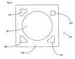
- Figure 8depicts, in plan, a substrate table from above.
- Figure 1schematically depicts a lithographic apparatus according to one embodiment of the invention.
- the apparatuscomprises:
- the illumination systemmay include various types of optical components, such as refractive, reflective, magnetic, electromagnetic, electrostatic or other types of optical components, or any combination thereof, for directing, shaping, or controlling radiation.
- optical componentssuch as refractive, reflective, magnetic, electromagnetic, electrostatic or other types of optical components, or any combination thereof, for directing, shaping, or controlling radiation.
- the support structureholds the patterning device in a manner that depends on the orientation of the patterning device, the design of the lithographic apparatus, and other conditions, such as for example whether or not the patterning device is held in a vacuum environment.
- the support structurecan use mechanical, vacuum, electrostatic or other clamping techniques to hold the patterning device.
- the support structuremay be a frame or a table, for example, which may be fixed or movable as required.
- the support structuremay ensure that the patterning device is at a desired position, for example with respect to the projection system. Any use of the terms "reticle” or “mask” herein may be considered synonymous with the more general term "patterning device.”
- patterning deviceused herein should be broadly interpreted as referring to any device that can be used to impart a radiation beam with a pattern in its cross-section such as to create a pattern in a target portion of the substrate. It should be noted that the pattern imparted to the radiation beam may not exactly correspond to the desired pattern in the target portion of the substrate, for example if the pattern includes phase-shifting features or so called assist features. Generally, the pattern imparted to the radiation beam will correspond to a particular functional layer in a device being created in the target portion, such as an integrated circuit.
- the patterning devicemay be transmissive or reflective.
- Examples of patterning devicesinclude masks, programmable mirror arrays, and programmable LCD panels.
- Masksare well known in lithography, and include mask types such as binary, alternating phase-shift, and attenuated phase-shift, as well as various hybrid mask types.
- An example of a programmable mirror arrayemploys a matrix arrangement of small mirrors, each of which can be individually tilted so as to reflect an incoming radiation beam in different directions. The tilted mirrors impart a pattern in a radiation beam which is reflected by the mirror matrix.
- projection systemused herein should be broadly interpreted as encompassing any type of projection system, including refractive, reflective, catadioptric, magnetic, electromagnetic and electrostatic optical systems, or any combination thereof, as appropriate for the exposure radiation being used, or for other factors such as the use of an immersion liquid or the use of a vacuum. Any use of the term “projection lens” herein may be considered as synonymous with the more general term “projection system”.
- the apparatusis of a transmissive type (e.g. employing a transmissive mask).
- the apparatusmay be of a reflective type (e.g. employing a programmable mirror array of a type as referred to above, or employing a reflective mask).
- the lithographic apparatusmay be of a type having two (dual stage) or more substrate tables (and/or two or more support structures). In such "multiple stage” machines the additional tables may be used in parallel, or preparatory steps may be carried out on one or more tables while one or more other tables are being used for exposure.
- the illuminator ILreceives a radiation beam from a radiation source SO.
- the source and the lithographic apparatusmay be separate entities, for example when the source is an excimer laser. In such cases, the source is not considered to form part of the lithographic apparatus and the radiation beam is passed from the source SO to the illuminator IL with the aid of a beam delivery system BD comprising, for example, suitable directing mirrors and/or a beam expander. In other cases the source may be an integral part of the lithographic apparatus, for example when the source is a mercury lamp.
- the source SO and the illuminator IL, together with the beam delivery system BD if required,may be referred to as a radiation system.
- the illuminator ILmay comprise an adjuster AM for adjusting the angular intensity distribution of the radiation beam.
- an adjuster AMfor adjusting the angular intensity distribution of the radiation beam.
- the illuminator ILmay comprise various other components, such as an integrator IN and a condenser CO.
- the illuminatormay be used to condition the radiation beam, to have a desired uniformity and intensity distribution in its cross-section.
- the radiation beam Bis incident on the patterning device (e.g., mask MA), which is held on the support structure (e.g., mask table MT), and is patterned by the patterning device. Having traversed the patterning device MA, the radiation beam B passes through the projection system PS, which focuses the beam onto a target portion C of the substrate W.
- the substrate table WTcan be moved accurately, e.g. so as to position different target portions C in the path of the radiation beam B.
- the first positioner PM and another position sensorcan be used to accurately position the patterning device MA with respect to the path of the radiation beam B, e.g. after mechanical retrieval from a mask library, or during a scan.
- movement of the support structure MTmay be realized with the aid of a long-stroke module (coarse positioning) and a short-stroke module (fine positioning), which form part of the first positioner PM.
- movement of the substrate table WTmay be realized using a long-stroke module and a short-stroke module, which form part of the second positioner PW.
- the support structure MTmay be connected to a short-stroke actuator only, or may be fixed.
- Mask MA and substrate Wmay be aligned using patterning device alignment marks M1, M2 and substrate alignment marks P1, P2.
- the substrate alignment marks as illustratedoccupy dedicated target portions, they may be located in spaces between target portions (these are known as scribe-lane alignment marks).
- the patterning device alignment marksmay be located between the dies.
- the depicted apparatuscould be used in at least one of the following modes:
- a further immersion lithography solution with a localized liquid supply systemis shown in Figure 4.
- Liquidis supplied by two groove inlets IN on either side of the projection system PL and is removed by a plurality of discrete outlets OUT arranged radially outwardly of the inlets IN.
- the inlets IN and OUTcan be arranged in a plate with a hole in its center and through which the projection beam is projected.
- Liquidis supplied by one groove inlet IN on one side of the projection system PL and removed by a plurality of discrete outlets OUT on the other side of the projection system PL, causing a flow of a thin film of liquid between the projection system PL and the substrate W.
- the choice of which combination of inlet IN and outlets OUT to usecan depend on the direction of movement of the substrate W (the other combination of inlet IN and outlets OUT being inactive).
- FIG. 5Another immersion lithography solution with a localized liquid supply system solution which has been proposed is to provide the liquid supply system with a liquid confinement structure which extends along at least a part of a boundary of the space between the final element of the projection system and the substrate table.
- a liquid confinement structurewhich extends along at least a part of a boundary of the space between the final element of the projection system and the substrate table.
- FIG. 5A seal is formed between the liquid confinement structure and the surface of the substrate.
- the sealis a contactless seal such as a gas seal.
- a gas sealis disclosed in US 2004 207 824 .
- Figure 5depicts an arrangement of a reservoir 10, which forms a contactless seal to the substrate around the image field of the projection system so that liquid 11 is confined to fill a space between the substrate surface and the final element of the projection system.
- a liquid confinement structure 12 positioned below and surrounding the final element of the projection system PLforms the reservoir. Liquid is brought into the space below the projection system and within the liquid confinement structure 12.
- the liquid confinement structure 12extends a little above the final element of the projection system and the liquid level rises above the final element so that a buffer of liquid is provided.
- the liquid confinement structure 12has an inner periphery that at the upper end preferably closely conforms to the shape of the projection system or the final element thereof and may, e.g., be round. At the bottom, the inner periphery closely conforms to the shape of the image field, e.g., rectangular though this need not be the case.
- the liquidis confined in the reservoir by a gas seal 16 between the bottom of the liquid confinement structure 12 and the surface of the substrate W.
- the gas sealis formed by gas, e.g. air, synthetic air, N 2 or an inert gas, provided under pressure via inlet 15 to the gap between liquid confinement structure 12 and substrate and extracted via outlet 14.
- gase.g. air, synthetic air, N 2 or an inert gas
- the overpressure on the gas inlet 15, vacuum level on the outlet 14 and geometry of the gapare arranged so that there is a high-velocity gas flow inwards that confines the liquid.
- other types of sealcould be used to contain the liquid such as simply an outlet to remove liquid and/or gas.
- FIG. 6illustrates a substrate table WT.
- the substrate table WTcomprises a substrate table body MB, which in an embodiment is a mirror block that carries one or mirrors for an interferometer system such that the position of the substrate W can be calculated.
- the substrate table body MBmay also house one or more actuators configured to position the substrate W.
- the substrate Wis held by a substrate support SS which is positioned in a recess 80 in the top surface of the substrate table body MB.
- the substrate support SSis conventionally a so called pimple or burl table which comprises a plurality of projections on upper and lower surfaces. A vacuum or under pressure is applied in the regions between the pimples to hold the substrate support SS to the substrate table body MB and to hold the substrate W to the substrate support SS.
- the substrate support SSmay be integral to the substrate table body MB.
- the substrate table WTis to be used in an immersion lithography apparatus in which liquid is provided between the projection system PS and the substrate W
- the substrate tablefurther comprises a cover plate 100 which is placed on the top surface of the substrate table body MB.
- the cover plate 100provides a flat and continuous upper surface so that a liquid supply system of the localized area type (i.e. one which provides liquid to only a localized area of the substrate W at one time) can be used.
- the top surface of the cover plate 100is substantially co-planar with the top surface of the substrate W (and also with the top surface of any sensor which might be positioned in recesses in the top surface of the substrate table body MB, as is shown in Figure 8 and described below).
- the cover plate 100may be integral to the substrate table body MB.
- a seal projection 200may be provided to extend between the bottom inner edge of the cover plate 100 and the top surface of the substrate support SS. The arrangement can be seen in detail in Figure 7.
- the substrate support SSmay be removed from the substrate table body MB without major dismantling of the substrate table WT.
- a removable and/or deactiveatable seal projection 200 between the cover plate 100 and the substrate support SSmay be provided.
- the cover plate 100may also be removably mounted on the top surface of the substrate table body MB so that elements of the substrate table WT protected by the cover plate 100 may easily be serviced.
- the cover plate 100comprises a cover plate projection 110 which is a so called edge seal member as is described in, for example, European Patent EP1486828 . The most basic form of this edge seal member is illustrated in Figure 7. Other types of edge seal member and/or different configurations may also be used.
- the seal projection 200is provided with an extremity 211 that is generally semi-circular in shape. This is depicted in more detail in Figure 7A.
- the extremityBy providing the extremity with a semi-circular cross-section, the total surface of the seal projection 200 that is exposed to a pressure difference, in particular the extremity 211 that on a bottom side thereof is exposed the low pressure inlet 85, is increased. This will result in a larger force that assists in clamping the seal projection 200 onto the substrate support SS.
- the extremity 211can be made out of the same material of the seal projection member 200, however it may also be made of any other suitable material.
- a separate force member 212is provided that can exert a force on the seal projection member 200. This is shown in more detail in Figure 7B.
- the force member 212is attached to the substrate support SS and its free end contacts the seal projection 200.
- the force member 212which may be made of a resilient material, for example a similar material as the material of the seal projection 200, contacting the seal projection 200, an additional clamping force can be exerted that assists in clamping the seal projection 200 onto the substrate support SS.
- the seal projection 200extends between the bottom surface of the cover plate 100, in an embodiment below the cover plate projection 110 as is illustrated, and the top surface of the substrate support SS. In an embodiment, the seal projection 200 extends around the whole periphery of the substrate support SS in one piece. This may be an optimum arrangement for liquid tightness.
- the material of the seal projection 200is flexible such that forces in all directions, but particularly in the Z direction cannot be transmitted between the substrate table SS and the cover plate 100, i.e. the seal is decoupled from the cover plate 100 and the substrate support SS substantially in the direction of the optical axis of the lithographic apparatus. In an embodiment, the flexible seal will exert a maximum force of less than about 1N/m of the seal.
- One end of the seal projection 200is attached to the cover plate by a bead of adhesive 220.
- Other ways of attaching the seal in a liquid tight mannermay also be used.
- the other end of the seal projection 200is attracted to the substrate support SS and releasably held there by a clamping device, in the illustrated example in the form of a low pressure inlet 85.
- the clamping devicemay be of any type, including, for example, an electromagnetic clamping device, an electrostatic clamping device and/or a removable adhesive.
- the cover platemay be removed and the seal projection 200 may be remotely activated or deactivated.
- a substantially non-flexible portion 210(a portion that is at least less flexible than the flexible seal projection 200) is positioned at the free end of the seal projection 200 which protrudes from the cover plate 100.
- the non-flexible portionmay, for example, be a metal part which is adhered to the top surface of the flexible material of the flexible seal projection 200.
- the substrate support SSwhich may be a wet low pressure inlet (not illustrated) because such a good seal may not easily be achieved between the cover plate 100 and the substrate W and consequently liquid may enter the gap between the substrate W and the substrate support SS.
- the non-flexible portion 210partly fills the gap between the flexible portion, the substrate support SS, cover plate 100 and the substrate W. In an embodiment, this gap is minimized for optimal performance of the liquid supply system.
- the seal projection 200 and/or the non-flexible portion 210is made of a polymeric flexible or elastic material which is resistant to the radiation of the lithographic apparatus.
- the seal projection 200 and/or the non-flexible portion 210may also be made of metal. Even rubber may be used, for example, if the cover plate projection 110 protects the seal projection 200 and/or the non-flexible portion 210 from irradiation by the projection beam B.
- the non-flexible portion 210, the semi-circular shaped extremity 211 and the force member 212may shield the seal projection 200 from the radiation of the projection beam B such that a material may be chosen for the seal projection 200 which is not resistant to the radiation of the projection system.
- the strength of the clamping device(the low pressure clamping device 85 in the embodiment) is about 25N/m to create a liquid tight seal with the material of the flexible seal projection 200 being rubber.
- Figure 8is a view in plan of the top surface of the substrate table WT. What can be seen is the top surface of the cover plate 100 with various orifices.
- the central circular orificeis the orifice for the recess 80 in which the substrate support SS is positioned.
- Various componentsare positioned around the central orifice and which are capable of being illuminated by the projection beam B of the projection system PS. These various components may be one or more sensors, including, for example, two transmission image sensors (TIS) 310, a spot sensor 330 and an integrated lens interferometer (ILIAS) 320.
- TIStransmission image sensors
- IASintegrated lens interferometer
- it is desirable that the cover plate 100may be easily removed from the substrate table body MB but there should also be a good seal between the cover plate 100, one or more of the sensors 310, 320, 330 and the substrate table body MB.
- sealis discussed herein in relation to sealing between the cover plate 100 and the substrate support SS and the substrate table body MB and a sensor 310, 320, 330, these are examples only and the types of seal discussed herein may be used to seal between any two parts of, in or on the substrate table and/or between the substrate table and the substrate W.
- any use of the terms "wafer” or “die” hereinmay be considered as synonymous with the more general terms “substrate” or “target portion”, respectively.
- the substrate referred to hereinmay be processed, before or after exposure, in for example a track (a tool that typically applies a layer of resist to a substrate and develops the exposed resist), a metrology tool and/or an inspection tool. Where applicable, the disclosure herein may be applied to such and other substrate processing tools. Further, the substrate may be processed more than once, for example in order to create a multi-layer IC, so that the term substrate used herein may also refer to a substrate that already contains multiple processed layers.
- imprint lithographya topography in a patterning device defines the pattern created on a substrate.
- the topography of the patterning devicemay be pressed into a layer of resist supplied to the substrate whereupon the resist is cured by applying electromagnetic radiation, heat, pressure or a combination thereof.
- the patterning deviceis moved out of the resist leaving a pattern in it after the resist is cured.
- radiationand “beam” used herein encompass all types of electromagnetic radiation, including ultraviolet (UV) radiation (e.g.
- the term "lens”, where the context allows,may refer to any one or combination of various types of optical components, including refractive, reflective, magnetic, electromagnetic and electrostatic optical components. While specific embodiments of the invention have been described above, it will be appreciated that the invention may be practiced otherwise than as described.
- the inventionmay take the form of a computer program containing one or more sequences of machine-readable instructions describing a method as disclosed above, or a data storage medium (e.g.
- a liquid supply systemis any mechanism that provides a liquid to a space between the projection system and the substrate and/or substrate table. It may comprise any combination of one or more structures, one or more liquid inlets, one or more gas inlets, one or more gas outlets, and/or one or more liquid outlets, the combination providing and confining the liquid to the space.
- a surface of the spacemay be limited to a portion of the substrate and/or substrate table, a surface of the space may completely cover a surface of the substrate and/or substrate table, or the space may envelop the substrate and/or substrate table.
Landscapes
- General Physics & Mathematics (AREA)
- Physics & Mathematics (AREA)
- Health & Medical Sciences (AREA)
- Epidemiology (AREA)
- Engineering & Computer Science (AREA)
- Environmental & Geological Engineering (AREA)
- Public Health (AREA)
- Toxicology (AREA)
- Atmospheric Sciences (AREA)
- Life Sciences & Earth Sciences (AREA)
- Exposure Of Semiconductors, Excluding Electron Or Ion Beam Exposure (AREA)
- Exposure And Positioning Against Photoresist Photosensitive Materials (AREA)
- Container, Conveyance, Adherence, Positioning, Of Wafer (AREA)
Description
- The present invention relates to a lithographic apparatus and a method for manufacturing a device.
- A lithographic apparatus is a machine that applies a desired pattern onto a substrate, usually onto a target portion of the substrate. A lithographic apparatus can be used, for example, in the manufacture of integrated circuits (ICs). In that instance, a patterning device, which is alternatively referred to as a mask or a reticle, may be used to generate a circuit pattern to be formed on an individual layer of the IC. This pattern can be transferred onto a target portion (e.g. comprising part of, one, or several dies) on a substrate (e.g. a silicon wafer). Transfer of the pattern is typically via imaging onto a layer of radiation-sensitive material (resist) provided on the substrate. In general, a single substrate will contain a network of adjacent target portions that are successively patterned. Known lithographic apparatus include so-called steppers, in which each target portion is irradiated by exposing an entire pattern onto the target portion at one time, and so-called scanners, in which each target portion is irradiated by scanning the pattern through a radiation beam in a given direction (the "scanning"-direction) while synchronously scanning the substrate parallel or anti-parallel to this direction. It is also possible to transfer the pattern from the patterning device to the substrate by imprinting the pattern onto the substrate.
- It has been proposed to immerse the substrate in the lithographic projection apparatus in a liquid having a relatively high refractive index, e.g. water, so as to fill a space between the final element of the projection system and the substrate. The point of this is to enable imaging of smaller features since the exposure radiation will have a shorter wavelength in the liquid. (The effect of the liquid may also be regarded as increasing the effective NA of the system and also increasing the depth of focus.) Other immersion liquids have been proposed, including water with solid particles (e.g. quartz) suspended therein.
- However, submersing the substrate or substrate and substrate table in a bath of liquid (see, for example,
United States patent US 4,509,852 , means that there is a large body of liquid that must be accelerated during a scanning exposure. This requires additional or more powerful motors and turbulence in the liquid may lead to undesirable and unpredictable effects. - One of the solutions proposed is for a liquid supply system to provide liquid on only a localized area of the substrate and in between the final element of the projection system and the substrate (the substrate generally has a larger surface area than the final element of the projection system). One way which has been proposed to arrange for this is disclosed in
PCT patent application WO 99/49504 - Of course handling liquids in an immersion apparatus creates specific difficulties. In particular, delicate parts of the substrate table must be liquidproofed against ingress of immersion liquid.
EP-A-1,429,188 discloses a seal between a substrate table and a substrate.EP-A-0,860,861 discloses a lithographic projection apparatus in accordance with the pre-characterising section ofclaim 1.- Accordingly, it would be advantageous, for example, to seal between different parts of the substrate table. In particular, it is desirable to have seals which do not transmit forces between the parts of the substrate table between which the seals extend.
- According to an aspect of the invention, there is provided a lithographic projection apparatus, comprising:
- a substrate table configured to hold a substrate;
- a first part of the substrate table having a flexible projection attached; and
- characterised in that
- a second part of the substrate table having a clamping device configured to attract and hold a free end of the projection to create a seal between the first part and the second part.
- According to an aspect of the invention, there is provided a device manufacturing .method, comprising:
- clamping an end of a flexible projection using a clamping device positioned on a first part of a substrate table to attract and hold said projection thereby to form a seal between the first part and a second part of the substrate table to which said flexible projection is attached; and
- projecting a patterned beam of radiation onto a substrate held on the substrate table.
- Embodiments of the invention will now be described, by way of example only, with reference to the accompanying schematic drawings in which corresponding reference symbols indicate corresponding parts, and in which:
- Figure 1 depicts a lithographic apparatus according to an embodiment of the invention;
- Figures 2 and 3 depict a liquid supply system for used in a lithographic projection apparatus;
- Figure 4 depicts another liquid supply system for use in a lithographic projection apparatus;
- Figure 5 depicts a further liquid supply system for use in a lithographic projection apparatus;
- Figure 6 depicts, in cross-section, a substrate table according to an embodiment of the present invention;
- Figure 7 depicts, in cross-section, a seal between a cover plate and a substrate support of a substrate table according to an embodiment of the present invention;
- Figure 7A depicts, in cross-section, a further seal between a cover plate and a substrate support of a substrate table according to an embodiment of the present invention;
- Figure 7B depicts, in cross-section, a further seal between a cover plate and a substrate support of a substrate table according to an embodiment of the present invention; and
- Figure 8 depicts, in plan, a substrate table from above.
- Figure 1 schematically depicts a lithographic apparatus according to one embodiment of the invention. The apparatus comprises:
- an illumination system (illuminator) IL configured to condition a radiation beam B (e.g. UV radiation or DUV radiation).
- a support structure (e.g. a mask table) MT constructed to hold a patterning device (e.g. a mask) MA and connected to a first positioner PM configured to accurately position the patterning device in accordance with certain parameters;
- a substrate table (e.g. a wafer table) WT constructed to hold a substrate (e.g. a resist-coated wafer) W and connected to a second positioner PW configured to accurately position the substrate in accordance with certain parameters; and
- a projection system (e.g. a refractive projection lens system) PS configured to project a pattern imparted to the radiation beam B by patterning device MA onto a target portion C (e.g. comprising one or more dies) of the substrate W.
- The illumination system may include various types of optical components, such as refractive, reflective, magnetic, electromagnetic, electrostatic or other types of optical components, or any combination thereof, for directing, shaping, or controlling radiation.
- The support structure holds the patterning device in a manner that depends on the orientation of the patterning device, the design of the lithographic apparatus, and other conditions, such as for example whether or not the patterning device is held in a vacuum environment. The support structure can use mechanical, vacuum, electrostatic or other clamping techniques to hold the patterning device. The support structure may be a frame or a table, for example, which may be fixed or movable as required. The support structure may ensure that the patterning device is at a desired position, for example with respect to the projection system. Any use of the terms "reticle" or "mask" herein may be considered synonymous with the more general term "patterning device."
- The term "patterning device" used herein should be broadly interpreted as referring to any device that can be used to impart a radiation beam with a pattern in its cross-section such as to create a pattern in a target portion of the substrate. It should be noted that the pattern imparted to the radiation beam may not exactly correspond to the desired pattern in the target portion of the substrate, for example if the pattern includes phase-shifting features or so called assist features. Generally, the pattern imparted to the radiation beam will correspond to a particular functional layer in a device being created in the target portion, such as an integrated circuit.
- The patterning device may be transmissive or reflective. Examples of patterning devices include masks, programmable mirror arrays, and programmable LCD panels. Masks are well known in lithography, and include mask types such as binary, alternating phase-shift, and attenuated phase-shift, as well as various hybrid mask types. An example of a programmable mirror array employs a matrix arrangement of small mirrors, each of which can be individually tilted so as to reflect an incoming radiation beam in different directions. The tilted mirrors impart a pattern in a radiation beam which is reflected by the mirror matrix.
- The term "projection system" used herein should be broadly interpreted as encompassing any type of projection system, including refractive, reflective, catadioptric, magnetic, electromagnetic and electrostatic optical systems, or any combination thereof, as appropriate for the exposure radiation being used, or for other factors such as the use of an immersion liquid or the use of a vacuum. Any use of the term "projection lens" herein may be considered as synonymous with the more general term "projection system".
- As here depicted, the apparatus is of a transmissive type (e.g. employing a transmissive mask). Alternatively, the apparatus may be of a reflective type (e.g. employing a programmable mirror array of a type as referred to above, or employing a reflective mask).
- The lithographic apparatus may be of a type having two (dual stage) or more substrate tables (and/or two or more support structures). In such "multiple stage" machines the additional tables may be used in parallel, or preparatory steps may be carried out on one or more tables while one or more other tables are being used for exposure.
- Referring to Figure 1, the illuminator IL receives a radiation beam from a radiation source SO. The source and the lithographic apparatus may be separate entities, for example when the source is an excimer laser. In such cases, the source is not considered to form part of the lithographic apparatus and the radiation beam is passed from the source SO to the illuminator IL with the aid of a beam delivery system BD comprising, for example, suitable directing mirrors and/or a beam expander. In other cases the source may be an integral part of the lithographic apparatus, for example when the source is a mercury lamp. The source SO and the illuminator IL, together with the beam delivery system BD if required, may be referred to as a radiation system.
- The illuminator IL may comprise an adjuster AM for adjusting the angular intensity distribution of the radiation beam. Generally, at least the outer and/or inner radial extent (commonly referred to as σ-outer and σ-inner, respectively) of the intensity distribution in a pupil plane of the illuminator can be adjusted. In addition, the illuminator IL may comprise various other components, such as an integrator IN and a condenser CO. The illuminator may be used to condition the radiation beam, to have a desired uniformity and intensity distribution in its cross-section.
- The radiation beam B is incident on the patterning device (e.g., mask MA), which is held on the support structure (e.g., mask table MT), and is patterned by the patterning device. Having traversed the patterning device MA, the radiation beam B passes through the projection system PS, which focuses the beam onto a target portion C of the substrate W. With the aid of the second positioner PW and position sensor IF (e.g. an interferometric device, linear encoder or capacitive sensor), the substrate table WT can be moved accurately, e.g. so as to position different target portions C in the path of the radiation beam B. Similarly, the first positioner PM and another position sensor (which is not explicitly depicted in Figure 1) can be used to accurately position the patterning device MA with respect to the path of the radiation beam B, e.g. after mechanical retrieval from a mask library, or during a scan. In general, movement of the support structure MT may be realized with the aid of a long-stroke module (coarse positioning) and a short-stroke module (fine positioning), which form part of the first positioner PM. Similarly, movement of the substrate table WT may be realized using a long-stroke module and a short-stroke module, which form part of the second positioner PW. In the case of a stepper (as opposed to a scanner) the support structure MT may be connected to a short-stroke actuator only, or may be fixed. Mask MA and substrate W may be aligned using patterning device alignment marks M1, M2 and substrate alignment marks P1, P2. Although the substrate alignment marks as illustrated occupy dedicated target portions, they may be located in spaces between target portions (these are known as scribe-lane alignment marks). Similarly, in situations in which more than one die is provided on the patterning device MA, the patterning device alignment marks may be located between the dies.
- The depicted apparatus could be used in at least one of the following modes:
- 1. In step mode, the support structure MT and the substrate table WT are kept essentially stationary, while an entire pattern imparted to the radiation beam is projected onto a target portion C at one time (i.e. a single static exposure). The substrate table WT is then shifted in the X and/or Y direction so that a different target portion C can be exposed. In step mode, the maximum size of the exposure field limits the size of the target portion C imaged in a single static exposure.
- 2. In scan mode, the support structure MT and the substrate table WT are scanned synchronously while a pattern imparted to the radiation beam is projected onto a target portion C (i.e. a single dynamic exposure). The velocity and direction of the substrate table WT relative to the support structure MT may be determined by the (de-)magnification and image reversal characteristics of the projection system PS. In scan mode, the maximum size of the exposure field limits the width (in the non-scanning direction) of the target portion in a single dynamic exposure, whereas the length of the scanning motion determines the height (in the scanning direction) of the target portion.
- 3. In another mode, the support structure MT is kept essentially stationary holding a programmable patterning device, and the substrate table WT is moved or scanned while a pattern imparted to the radiation beam is projected onto a target portion C. In this mode, generally a pulsed radiation source is employed and the programmable patterning device is updated as required after each movement of the substrate table WT or in between successive radiation pulses during a scan. This mode of operation can be readily applied to maskless lithography that utilizes programmable patterning device, such as a programmable mirror array of a type as referred to above.
- Combinations and/or variations on the above described modes of use or entirely different modes of use may also be employed.
- A further immersion lithography solution with a localized liquid supply system is shown in Figure 4. Liquid is supplied by two groove inlets IN on either side of the projection system PL and is removed by a plurality of discrete outlets OUT arranged radially outwardly of the inlets IN. The inlets IN and OUT can be arranged in a plate with a hole in its center and through which the projection beam is projected. Liquid is supplied by one groove inlet IN on one side of the projection system PL and removed by a plurality of discrete outlets OUT on the other side of the projection system PL, causing a flow of a thin film of liquid between the projection system PL and the substrate W. The choice of which combination of inlet IN and outlets OUT to use can depend on the direction of movement of the substrate W (the other combination of inlet IN and outlets OUT being inactive).
- Another immersion lithography solution with a localized liquid supply system solution which has been proposed is to provide the liquid supply system with a liquid confinement structure which extends along at least a part of a boundary of the space between the final element of the projection system and the substrate table. Such a system is shown in Figure 5. The liquid confinement structure is substantially stationary relative to the projection system in the XY plane though there may be some relative movement in the Z direction (in the direction of the optical axis). A seal is formed between the liquid confinement structure and the surface of the substrate. In an embodiment, the seal is a contactless seal such as a gas seal. Such a system with a gas seal is disclosed in
US 2004 207 824 . - Figure 5 depicts an arrangement of a
reservoir 10, which forms a contactless seal to the substrate around the image field of the projection system so that liquid 11 is confined to fill a space between the substrate surface and the final element of the projection system. Aliquid confinement structure 12 positioned below and surrounding the final element of the projection system PL forms the reservoir. Liquid is brought into the space below the projection system and within theliquid confinement structure 12. Theliquid confinement structure 12 extends a little above the final element of the projection system and the liquid level rises above the final element so that a buffer of liquid is provided. Theliquid confinement structure 12 has an inner periphery that at the upper end preferably closely conforms to the shape of the projection system or the final element thereof and may, e.g., be round. At the bottom, the inner periphery closely conforms to the shape of the image field, e.g., rectangular though this need not be the case. - The liquid is confined in the reservoir by a
gas seal 16 between the bottom of theliquid confinement structure 12 and the surface of the substrate W. The gas seal is formed by gas, e.g. air, synthetic air, N2 or an inert gas, provided under pressure viainlet 15 to the gap betweenliquid confinement structure 12 and substrate and extracted viaoutlet 14. The overpressure on thegas inlet 15, vacuum level on theoutlet 14 and geometry of the gap are arranged so that there is a high-velocity gas flow inwards that confines the liquid. It will be understood by the person skilled in the art that other types of seal could be used to contain the liquid such as simply an outlet to remove liquid and/or gas. - Figure 6 illustrates a substrate table WT. The substrate table WT comprises a substrate table body MB, which in an embodiment is a mirror block that carries one or mirrors for an interferometer system such that the position of the substrate W can be calculated. The substrate table body MB may also house one or more actuators configured to position the substrate W. The substrate W is held by a substrate support SS which is positioned in a
recess 80 in the top surface of the substrate table body MB. The substrate support SS is conventionally a so called pimple or burl table which comprises a plurality of projections on upper and lower surfaces. A vacuum or under pressure is applied in the regions between the pimples to hold the substrate support SS to the substrate table body MB and to hold the substrate W to the substrate support SS. In an embodiment, the substrate support SS may be integral to the substrate table body MB. - Since this substrate table WT is to be used in an immersion lithography apparatus in which liquid is provided between the projection system PS and the substrate W, the substrate table further comprises a
cover plate 100 which is placed on the top surface of the substrate table body MB. Thecover plate 100 provides a flat and continuous upper surface so that a liquid supply system of the localized area type (i.e. one which provides liquid to only a localized area of the substrate W at one time) can be used. Thus the top surface of thecover plate 100 is substantially co-planar with the top surface of the substrate W (and also with the top surface of any sensor which might be positioned in recesses in the top surface of the substrate table body MB, as is shown in Figure 8 and described below). In an embodiment, thecover plate 100 may be integral to the substrate table body MB. - In order to reduce or prevent ingress of liquid into the
recess 80 between the substrate support SS and the substrate table body MB, aseal projection 200 may be provided to extend between the bottom inner edge of thecover plate 100 and the top surface of the substrate support SS. The arrangement can be seen in detail in Figure 7. - In an embodiment, it is useful that the substrate support SS may be removed from the substrate table body MB without major dismantling of the substrate table WT. For this reason, for example, a removable and/or
deactiveatable seal projection 200 between thecover plate 100 and the substrate support SS may be provided. Thecover plate 100 may also be removably mounted on the top surface of the substrate table body MB so that elements of the substrate table WT protected by thecover plate 100 may easily be serviced. Thecover plate 100 comprises acover plate projection 110 which is a so called edge seal member as is described in, for example,European Patent EP1486828 . The most basic form of this edge seal member is illustrated in Figure 7. Other types of edge seal member and/or different configurations may also be used. - According to an alternative or additional embodiment of the present invention the
seal projection 200 is provided with anextremity 211 that is generally semi-circular in shape. This is depicted in more detail in Figure 7A. By providing the extremity with a semi-circular cross-section, the total surface of theseal projection 200 that is exposed to a pressure difference, in particular theextremity 211 that on a bottom side thereof is exposed thelow pressure inlet 85, is increased. This will result in a larger force that assists in clamping theseal projection 200 onto the substrate support SS. Theextremity 211 can be made out of the same material of theseal projection member 200, however it may also be made of any other suitable material. - According to a further alternative or additional embodiment of the present invention a
separate force member 212 is provided that can exert a force on theseal projection member 200. This is shown in more detail in Figure 7B. Theforce member 212 is attached to the substrate support SS and its free end contacts theseal projection 200.
With theforce member 212, which may be made of a resilient material, for example a similar material as the material of theseal projection 200, contacting theseal projection 200, an additional clamping force can be exerted that assists in clamping theseal projection 200 onto the substrate support SS. - The
seal projection 200 extends between the bottom surface of thecover plate 100, in an embodiment below thecover plate projection 110 as is illustrated, and the top surface of the substrate support SS. In an embodiment, theseal projection 200 extends around the whole periphery of the substrate support SS in one piece. This may be an optimum arrangement for liquid tightness. The material of theseal projection 200 is flexible such that forces in all directions, but particularly in the Z direction cannot be transmitted between the substrate table SS and thecover plate 100, i.e. the seal is decoupled from thecover plate 100 and the substrate support SS substantially in the direction of the optical axis of the lithographic apparatus. In an embodiment, the flexible seal will exert a maximum force of less than about 1N/m of the seal. One end of theseal projection 200 is attached to the cover plate by a bead ofadhesive 220. Other ways of attaching the seal in a liquid tight manner may also be used. The other end of theseal projection 200 is attracted to the substrate support SS and releasably held there by a clamping device, in the illustrated example in the form of alow pressure inlet 85. The clamping device may be of any type, including, for example, an electromagnetic clamping device, an electrostatic clamping device and/or a removable adhesive. Thus, the cover plate may be removed and theseal projection 200 may be remotely activated or deactivated. - In order to achieve a good seal between the
flexible seal projection 200 and the substrate support SS, a substantially non-flexible portion 210 (a portion that is at least less flexible than the flexible seal projection 200) is positioned at the free end of theseal projection 200 which protrudes from thecover plate 100. The non-flexible portion may, for example, be a metal part which is adhered to the top surface of the flexible material of theflexible seal projection 200. Thus, when thelow pressure inlet 85 is activated, theflexible seal projection 200 will bend down so that the flexible material is clamped between thenon-flexible member 210 and thelow pressure inlet 85 to produce a good seal. In this way, thelow pressure inlet 85 of the clamping device may be a totally dry low pressure inlet as liquid can be prevented from entering it. This is likely in contrast to the low pressure inlet used by the substrate support SS which may be a wet low pressure inlet (not illustrated) because such a good seal may not easily be achieved between thecover plate 100 and the substrate W and consequently liquid may enter the gap between the substrate W and the substrate support SS. Thenon-flexible portion 210 partly fills the gap between the flexible portion, the substrate support SS,cover plate 100 and the substrate W. In an embodiment, this gap is minimized for optimal performance of the liquid supply system. - In an embodiment, the
seal projection 200 and/or thenon-flexible portion 210 is made of a polymeric flexible or elastic material which is resistant to the radiation of the lithographic apparatus. Theseal projection 200 and/or thenon-flexible portion 210 may also be made of metal. Even rubber may be used, for example, if thecover plate projection 110 protects theseal projection 200 and/or thenon-flexible portion 210 from irradiation by the projection beam B. - In an embodiment, the
non-flexible portion 210, the semi-circular shapedextremity 211 and theforce member 212, may shield theseal projection 200 from the radiation of the projection beam B such that a material may be chosen for theseal projection 200 which is not resistant to the radiation of the projection system. - In an embodiment, the strength of the clamping device (the low
pressure clamping device 85 in the embodiment) is about 25N/m to create a liquid tight seal with the material of theflexible seal projection 200 being rubber. - Further details of the substrate table WT according to an embodiment of the present invention are illustrated with reference to Figure 8. Figure 8 is a view in plan of the top surface of the substrate table WT. What can be seen is the top surface of the
cover plate 100 with various orifices. The central circular orifice is the orifice for therecess 80 in which the substrate support SS is positioned. Various components are positioned around the central orifice and which are capable of being illuminated by the projection beam B of the projection system PS. These various components may be one or more sensors, including, for example, two transmission image sensors (TIS) 310, aspot sensor 330 and an integrated lens interferometer (ILIAS) 320. In an embodiment, it is desirable that thecover plate 100 may be easily removed from the substrate table body MB but there should also be a good seal between thecover plate 100, one or more of thesensors - Although the seal is discussed herein in relation to sealing between the
cover plate 100 and the substrate support SS and the substrate table body MB and asensor - In
European Patent EP 1420 300 , the idea of a twin or dual stage immersion lithography apparatus is disclosed. Such an apparatus is provided with two tables for supporting a substrate. Leveling measurements are carried out with a table at a first position, without immersion liquid, and exposure is carried out with a table at a second position, where immersion liquid is present. Alternatively, the apparatus has only one table.
Although specific reference may be made in this text to the use of lithographic apparatus in the manufacture of ICs, it should be understood that the lithographic apparatus described herein may have other applications, such as the manufacture of integrated optical systems, guidance and detection patterns for magnetic domain memories, flat-panel displays, liquid-crystal displays (LCDs), thin-film magnetic heads, etc. The skilled artisan will appreciate that, in the context of such alternative applications, any use of the terms "wafer" or "die" herein may be considered as synonymous with the more general terms "substrate" or "target portion", respectively. The substrate referred to herein may be processed, before or after exposure, in for example a track (a tool that typically applies a layer of resist to a substrate and develops the exposed resist), a metrology tool and/or an inspection tool. Where applicable, the disclosure herein may be applied to such and other substrate processing tools. Further, the substrate may be processed more than once, for example in order to create a multi-layer IC, so that the term substrate used herein may also refer to a substrate that already contains multiple processed layers.
Although specific reference may have been made above to the use of embodiments of the invention in the context of optical lithography, it will be appreciated that the invention may be used in other applications, for example imprint lithography, and where the context allows, is not limited to optical lithography. In imprint lithography a topography in a patterning device defines the pattern created on a substrate. The topography of the patterning device may be pressed into a layer of resist supplied to the substrate whereupon the resist is cured by applying electromagnetic radiation, heat, pressure or a combination thereof. The patterning device is moved out of the resist leaving a pattern in it after the resist is cured.
The terms "radiation" and "beam" used herein encompass all types of electromagnetic radiation, including ultraviolet (UV) radiation (e.g. having a wavelength of or about 365, 248, 193, 157 or 126 nm) and extreme ultra-violet (EUV) radiation (e.g. having a wavelength in the range of 5-20 nm), as well as particle beams, such as ion beams or electron beams.
The term "lens", where the context allows, may refer to any one or combination of various types of optical components, including refractive, reflective, magnetic, electromagnetic and electrostatic optical components.
While specific embodiments of the invention have been described above, it will be appreciated that the invention may be practiced otherwise than as described. For example, the invention may take the form of a computer program containing one or more sequences of machine-readable instructions describing a method as disclosed above, or a data storage medium (e.g. semiconductor memory, magnetic or optical disk) having such a computer program stored therein.
One or more embodiments of the present invention may be applied to any immersion lithography apparatus, such as those types mentioned above, and whether the immersion liquid is provided in the form of a bath or only on a localized surface area of the substrate. A liquid supply system is any mechanism that provides a liquid to a space between the projection system and the substrate and/or substrate table. It may comprise any combination of one or more structures, one or more liquid inlets, one or more gas inlets, one or more gas outlets, and/or one or more liquid outlets, the combination providing and confining the liquid to the space. In an embodiment, a surface of the space may be limited to a portion of the substrate and/or substrate table, a surface of the space may completely cover a surface of the substrate and/or substrate table, or the space may envelop the substrate and/or substrate table.[00066] The descriptions above are intended to be illustrative, not limiting. Thus, it will be apparent to one skilled in the art that modifications may be made to the invention as described without departing from the scope of the claims set out below.
Claims (18)
- A lithographic projection apparatus, comprising:a substrate table (WT) configured to hold a substrate;a first part (100) of the substrate table having a flexible projection (200) attached thereto; andcharacterised in that
a second part (SS, 310, 320, 330) of the substrate table having a clamping device (85) configured to attract and hold a free end of the projection to create a seal between the first part and the second part. - The apparatus of claim 1, wherein the clamping device comprises a low pressure inlet.
- The apparatus of claim 1 or 2, wherein the flexible projection comprises a substantially non-flexible portion (210) proximal to the free end.
- The apparatus of claim 3, wherein the substantially non-flexible portion is made of a material substantially resistant to damage from radiation of the apparatus.
- The apparatus of any one of the preceding claims, wherein the flexible projection is adhered to the first part.
- The apparatus of any one of the preceding claims, wherein the first part comprises a cover plate configured to cover a portion of a top surface of the substrate table.
- The apparatus of any one of the preceding claims, wherein the second part is a substrate support configured to support the substrate on the substrate table.
- The apparatus of any one of the preceding claims, wherein the flexible projection surrounds the second part and the first part comprises a recess (80) in which the second part is positioned.
- The apparatus of any one of the preceding claims, wherein the flexible projection is made of a material substantially resistant to damage from radiation of the apparatus.
- The apparatus of any one of the preceding claims, wherein the first part comprises a cover plate projection (110), the flexible projection (200) and the cover plate projection (110) arranged so that in use the cover plate projection (110) substantially shields the flexible projection from radiation of the apparatus.
- The apparatus of any one of the preceding claims, further comprising:a projection system (PL) configured to project a patterned radiation beam onto a target portion of the substrate; anda liquid supply system (IH) configured to at least partly fill a space between the projection system and the substrate with a liquid.
- A device manufacturing method, comprising:providing a substrate table (WT) to hold a substrate, the substrate table comprising a first part (100), having a flexible projection (200) attached thereto, and a second part (SS, 310, 320, 330) having a clamping device,clamping a free end of the flexible projection (200) onto the second part, by using the clamping device (85) to attract and hold said flexible projection (200), to thereby form a seal between the first part (100) and the second part (SS, 310, 320, 330) of the substrate table, andprojecting a patterned beam of radiation onto the substrate.
- The method of claim 12, wherein the clamping is performed using a low pressure inlet.
- The method of claim 12 or 13, wherein the flexible projection comprises a substantially non-flexible portion (210) proximal to the end of the flexible projection.
- The method of claim 12, 13 or 14, wherein the flexible projection is adhered to the first part.
- The method of any one of claims 12-15, wherein the second part is a substrate support configured to support the substrate on the substrate table.
- The method of any one of claims 12-16, further comprising substantially shielding the flexible projection from radiation of the patterned radiation beam using a cover plate projection (110).
- The method of any one of claims 12-17, comprising projecting the patterned radiation beam through a liquid onto a target portion of the substrate.
Priority Applications (2)
| Application Number | Priority Date | Filing Date | Title |
|---|---|---|---|
| EP07007495AEP1821150B1 (en) | 2004-12-08 | 2005-12-01 | Lithographic apparatus and device manufacturing method |
| EP08012007.4AEP1970763A3 (en) | 2004-12-08 | 2005-12-01 | Lithographic apparatus and device manufacturing method |
Applications Claiming Priority (1)
| Application Number | Priority Date | Filing Date | Title |
|---|---|---|---|
| US11/006,550US7365827B2 (en) | 2004-12-08 | 2004-12-08 | Lithographic apparatus and device manufacturing method |
Related Child Applications (1)
| Application Number | Title | Priority Date | Filing Date |
|---|---|---|---|
| EP07007495ADivisionEP1821150B1 (en) | 2004-12-08 | 2005-12-01 | Lithographic apparatus and device manufacturing method |
Publications (2)
| Publication Number | Publication Date |
|---|---|
| EP1669807A1 EP1669807A1 (en) | 2006-06-14 |
| EP1669807B1true EP1669807B1 (en) | 2007-08-01 |
Family
ID=36084289
Family Applications (3)
| Application Number | Title | Priority Date | Filing Date |
|---|---|---|---|
| EP08012007.4AWithdrawnEP1970763A3 (en) | 2004-12-08 | 2005-12-01 | Lithographic apparatus and device manufacturing method |
| EP20050257410ActiveEP1669807B1 (en) | 2004-12-08 | 2005-12-01 | Lithographic apparatus and device manufacturing method |
| EP07007495ANot-in-forceEP1821150B1 (en) | 2004-12-08 | 2005-12-01 | Lithographic apparatus and device manufacturing method |
Family Applications Before (1)
| Application Number | Title | Priority Date | Filing Date |
|---|---|---|---|
| EP08012007.4AWithdrawnEP1970763A3 (en) | 2004-12-08 | 2005-12-01 | Lithographic apparatus and device manufacturing method |
Family Applications After (1)
| Application Number | Title | Priority Date | Filing Date |
|---|---|---|---|
| EP07007495ANot-in-forceEP1821150B1 (en) | 2004-12-08 | 2005-12-01 | Lithographic apparatus and device manufacturing method |
Country Status (8)
| Country | Link |
|---|---|
| US (3) | US7365827B2 (en) |
| EP (3) | EP1970763A3 (en) |
| JP (4) | JP4322865B2 (en) |
| KR (1) | KR100760316B1 (en) |
| CN (3) | CN101900951B (en) |
| DE (2) | DE602005001835T2 (en) |
| SG (2) | SG123683A1 (en) |
| TW (1) | TWI320876B (en) |
Cited By (1)
| Publication number | Priority date | Publication date | Assignee | Title |
|---|---|---|---|---|
| US7791709B2 (en) | 2006-12-08 | 2010-09-07 | Asml Netherlands B.V. | Substrate support and lithographic process |
Families Citing this family (17)
| Publication number | Priority date | Publication date | Assignee | Title |
|---|---|---|---|---|
| US7365827B2 (en)* | 2004-12-08 | 2008-04-29 | Asml Netherlands B.V. | Lithographic apparatus and device manufacturing method |
| US7352440B2 (en)* | 2004-12-10 | 2008-04-01 | Asml Netherlands B.V. | Substrate placement in immersion lithography |
| US7684010B2 (en) | 2005-03-09 | 2010-03-23 | Asml Netherlands B.V. | Lithographic apparatus, device manufacturing method, seal structure, method of removing an object and a method of sealing |
| US7633073B2 (en)* | 2005-11-23 | 2009-12-15 | Asml Netherlands B.V. | Lithographic apparatus and device manufacturing method |
| US7830498B2 (en)* | 2006-10-10 | 2010-11-09 | Hewlett-Packard Development Company, L.P. | Hydraulic-facilitated contact lithography apparatus, system and method |
| US20080137055A1 (en)* | 2006-12-08 | 2008-06-12 | Asml Netherlands B.V. | Lithographic apparatus and device manufacturing method |
| NL2004807A (en) | 2009-06-30 | 2011-01-04 | Asml Netherlands Bv | Substrate table for a lithographic apparatus, litographic apparatus, method of using a substrate table and device manufacturing method. |
| NL2005126A (en)* | 2009-09-21 | 2011-03-22 | Asml Netherlands Bv | Lithographic apparatus, coverplate and device manufacturing method. |
| NL2005120A (en)* | 2009-09-21 | 2011-03-22 | Asml Netherlands Bv | Lithographic apparatus, coverplate and device manufacturing method. |
| NL2005479A (en)* | 2009-11-17 | 2011-05-18 | Asml Netherlands Bv | Lithographic apparatus, removable member and device manufacturing method. |
| NL2005478A (en)* | 2009-11-17 | 2011-05-18 | Asml Netherlands Bv | Lithographic apparatus, removable member and device manufacturing method. |
| NL2006203A (en)* | 2010-03-16 | 2011-09-19 | Asml Netherlands Bv | Cover for a substrate table, substrate table for a lithographic apparatus, lithographic apparatus, and device manufacturing method. |
| NL2006244A (en)* | 2010-03-16 | 2011-09-19 | Asml Netherlands Bv | Lithographic apparatus, cover for use in a lithographic apparatus and method for designing a cover for use in a lithographic apparatus. |
| NL2006536A (en)* | 2010-05-13 | 2011-11-15 | Asml Netherlands Bv | A substrate table, a lithographic apparatus, a method of flattening an edge of a substrate and a device manufacturing method. |
| JP5313293B2 (en) | 2010-05-19 | 2013-10-09 | エーエスエムエル ネザーランズ ビー.ブイ. | Lithographic apparatus, fluid handling structure used in lithographic apparatus, and device manufacturing method |
| KR102003416B1 (en) | 2012-05-29 | 2019-07-24 | 에이에스엠엘 네델란즈 비.브이. | Support apparatus, lithographic apparatus and device manufacturing method |
| EP4018262B1 (en) | 2019-08-20 | 2023-06-21 | ASML Netherlands B.V. | Substrate holder and lithographic apparatus |
Family Cites Families (141)
| Publication number | Priority date | Publication date | Assignee | Title |
|---|---|---|---|---|
| DE224448C (en) | ||||
| DE206607C (en) | ||||
| DE242880C (en) | ||||
| DE221563C (en) | ||||
| US2759254A (en)* | 1953-08-17 | 1956-08-21 | Robert M Soehnlen | Method of connecting fluid pipes |
| GB1242527A (en)* | 1967-10-20 | 1971-08-11 | Kodak Ltd | Optical instruments |
| US3573975A (en)* | 1968-07-10 | 1971-04-06 | Ibm | Photochemical fabrication process |
| ATE1462T1 (en) | 1979-07-27 | 1982-08-15 | Werner W. Dr. Tabarelli | OPTICAL LITHOGRAPHY PROCESS AND DEVICE FOR COPYING A PATTERN ONTO A SEMICONDUCTOR DISC. |
| FR2474708B1 (en) | 1980-01-24 | 1987-02-20 | Dme | HIGH-RESOLUTION MICROPHOTOLITHOGRAPHY PROCESS |
| US4574697A (en) | 1980-08-11 | 1986-03-11 | Norwood Industries, Inc. | Sheet material for mounting printing plates |
| JPS5754317A (en)* | 1980-09-19 | 1982-03-31 | Hitachi Ltd | Method and device for forming pattern |
| US4346164A (en)* | 1980-10-06 | 1982-08-24 | Werner Tabarelli | Photolithographic method for the manufacture of integrated circuits |
| US4509852A (en)* | 1980-10-06 | 1985-04-09 | Werner Tabarelli | Apparatus for the photolithographic manufacture of integrated circuit elements |
| US4390273A (en)* | 1981-02-17 | 1983-06-28 | Censor Patent-Und Versuchsanstalt | Projection mask as well as a method and apparatus for the embedding thereof and projection printing system |
| JPS57153433A (en)* | 1981-03-18 | 1982-09-22 | Hitachi Ltd | Manufacturing device for semiconductor |
| JPS58202448A (en) | 1982-05-21 | 1983-11-25 | Hitachi Ltd | exposure equipment |
| DD206607A1 (en) | 1982-06-16 | 1984-02-01 | Mikroelektronik Zt Forsch Tech | METHOD AND DEVICE FOR ELIMINATING INTERFERENCE EFFECTS |
| DD242880A1 (en) | 1983-01-31 | 1987-02-11 | Kuch Karl Heinz | DEVICE FOR PHOTOLITHOGRAPHIC STRUCTURAL TRANSMISSION |
| DD221563A1 (en) | 1983-09-14 | 1985-04-24 | Mikroelektronik Zt Forsch Tech | IMMERSIONS OBJECTIVE FOR THE STEP-BY-STEP PROJECTION IMAGING OF A MASK STRUCTURE |
| DD224448A1 (en) | 1984-03-01 | 1985-07-03 | Zeiss Jena Veb Carl | DEVICE FOR PHOTOLITHOGRAPHIC STRUCTURAL TRANSMISSION |
| JPS6265326A (en) | 1985-09-18 | 1987-03-24 | Hitachi Ltd | Exposure device |
| JPS62121417A (en) | 1985-11-22 | 1987-06-02 | Hitachi Ltd | Immersion objective lens device |
| US4744634A (en)* | 1986-04-28 | 1988-05-17 | Hughes Aircraft Company | Method and apparatus for reducing the effects of vibrational disturbances on the frequency stability of a laser |
| JPS63157419A (en) | 1986-12-22 | 1988-06-30 | Toshiba Corp | Fine pattern transfer apparatus |
| US5040020A (en)* | 1988-03-31 | 1991-08-13 | Cornell Research Foundation, Inc. | Self-aligned, high resolution resonant dielectric lithography |
| JPH03209479A (en) | 1989-09-06 | 1991-09-12 | Sanee Giken Kk | Exposure method |
| US5121256A (en)* | 1991-03-14 | 1992-06-09 | The Board Of Trustees Of The Leland Stanford Junior University | Lithography system employing a solid immersion lens |
| JPH04305917A (en) | 1991-04-02 | 1992-10-28 | Nikon Corp | Close-contact exposure equipment |
| JPH04305915A (en) | 1991-04-02 | 1992-10-28 | Nikon Corp | Adhesion type exposure device |
| EP0606309B1 (en) | 1991-10-04 | 1995-08-30 | Alcan International Limited | Peelable laminated structures and process for production thereof |
| JP3151927B2 (en)* | 1992-04-10 | 2001-04-03 | 株式会社村田製作所 | Acceleration sensor |
| JPH06124873A (en) | 1992-10-09 | 1994-05-06 | Canon Inc | Immersion projection exposure system |
| JP2753930B2 (en)* | 1992-11-27 | 1998-05-20 | キヤノン株式会社 | Immersion type projection exposure equipment |
| JP2520833B2 (en) | 1992-12-21 | 1996-07-31 | 東京エレクトロン株式会社 | Immersion type liquid treatment device |
| US5354614A (en) | 1993-03-01 | 1994-10-11 | Minnesota Mining And Manufacturing Company | Masking tape with stiffened edge and method of gasket masking |
| JPH07220990A (en) | 1994-01-28 | 1995-08-18 | Hitachi Ltd | Pattern forming method and exposure apparatus thereof |
| US5476712A (en) | 1994-05-31 | 1995-12-19 | Avery Dennison Corporation | Flexographic plate mounting tape |
| JPH08316124A (en)* | 1995-05-19 | 1996-11-29 | Hitachi Ltd | Projection exposure method and exposure apparatus |
| US20050025609A1 (en) | 1996-01-03 | 2005-02-03 | Oxford J. Craig | Surface mount ring assembly for loudspeaker |
| US6104687A (en)* | 1996-08-26 | 2000-08-15 | Digital Papyrus Corporation | Method and apparatus for coupling an optical lens to a disk through a coupling medium having a relatively high index of refraction |
| US5825043A (en)* | 1996-10-07 | 1998-10-20 | Nikon Precision Inc. | Focusing and tilting adjustment system for lithography aligner, manufacturing apparatus or inspection apparatus |
| JP3612920B2 (en) | 1997-02-14 | 2005-01-26 | ソニー株式会社 | Exposure apparatus for producing an optical recording medium master |
| US5870271A (en) | 1997-02-19 | 1999-02-09 | Applied Materials, Inc. | Pressure actuated sealing diaphragm for chucks |
| JPH10255319A (en) | 1997-03-12 | 1998-09-25 | Hitachi Maxell Ltd | Master exposure apparatus and method |
| JP3747566B2 (en) | 1997-04-23 | 2006-02-22 | 株式会社ニコン | Immersion exposure equipment |
| JP3817836B2 (en) | 1997-06-10 | 2006-09-06 | 株式会社ニコン | EXPOSURE APPARATUS, ITS MANUFACTURING METHOD, EXPOSURE METHOD, AND DEVICE MANUFACTURING METHOD |
| US5900354A (en)* | 1997-07-03 | 1999-05-04 | Batchelder; John Samuel | Method for optical inspection and lithography |
| JPH11176727A (en) | 1997-12-11 | 1999-07-02 | Nikon Corp | Projection exposure equipment |
| EP1039511A4 (en) | 1997-12-12 | 2005-03-02 | Nikon Corp | Projection exposure method and projection aligner |
| WO1999049504A1 (en) | 1998-03-26 | 1999-09-30 | Nikon Corporation | Projection exposure method and system |
| JP2000058436A (en) | 1998-08-11 | 2000-02-25 | Nikon Corp | Projection exposure apparatus and exposure method |
| TWI242112B (en)* | 1999-04-19 | 2005-10-21 | Asml Netherlands Bv | Lithographic projection apparatus and method of operating a lithographic projection apparatus |
| TWI242111B (en)* | 1999-04-19 | 2005-10-21 | Asml Netherlands Bv | Gas bearings for use in vacuum chambers and their application in lithographic projection apparatus |
| JP4504479B2 (en) | 1999-09-21 | 2010-07-14 | オリンパス株式会社 | Immersion objective lens for microscope |
| TW504605B (en)* | 1999-12-03 | 2002-10-01 | Asm Lithography Bv | Lithographic projection apparatus, method of manufacturing a device using the same, the device and mask |
| JP2001272604A (en)* | 2000-03-27 | 2001-10-05 | Olympus Optical Co Ltd | Immersion objective lens and optical device using the same |
| TW591653B (en)* | 2000-08-08 | 2004-06-11 | Koninkl Philips Electronics Nv | Method of manufacturing an optically scannable information carrier |
| KR100866818B1 (en)* | 2000-12-11 | 2008-11-04 | 가부시키가이샤 니콘 | Projection optical system and exposure apparatus comprising the same |
| CN1423831A (en) | 2000-12-22 | 2003-06-11 | 株式会社尼康 | Wavefront aberration measuring instrument, wavefront aberration measuring method, exposure apparatus, and method for manufacturing microdevice |
| US6736406B1 (en)* | 2001-05-04 | 2004-05-18 | Brian G. Provencher | Self-adhesive gasket |
| US20020163629A1 (en)* | 2001-05-07 | 2002-11-07 | Michael Switkes | Methods and apparatus employing an index matching medium |
| US6600547B2 (en)* | 2001-09-24 | 2003-07-29 | Nikon Corporation | Sliding seal |
| US6897941B2 (en)* | 2001-11-07 | 2005-05-24 | Applied Materials, Inc. | Optical spot grid array printer |
| US20030089552A1 (en) | 2001-11-13 | 2003-05-15 | Sahawneh Nader F. | Flexible, water-proof flashing tape |
| DE10229818A1 (en)* | 2002-06-28 | 2004-01-15 | Carl Zeiss Smt Ag | Focus detection method and imaging system with focus detection system |
| DE10210899A1 (en) | 2002-03-08 | 2003-09-18 | Zeiss Carl Smt Ag | Refractive projection lens for immersion lithography |
| JP3613470B2 (en) | 2002-03-12 | 2005-01-26 | 船井電機株式会社 | Optical head |
| TWI249082B (en) | 2002-08-23 | 2006-02-11 | Nikon Corp | Projection optical system and method for photolithography and exposure apparatus and method using same |
| US6788477B2 (en)* | 2002-10-22 | 2004-09-07 | Taiwan Semiconductor Manufacturing Co., Ltd. | Apparatus for method for immersion lithography |
| DE60335595D1 (en)* | 2002-11-12 | 2011-02-17 | Asml Netherlands Bv | Immersion lithographic apparatus and method of making a device |
| EP1429188B1 (en) | 2002-11-12 | 2013-06-19 | ASML Netherlands B.V. | Lithographic projection apparatus |
| CN100568101C (en) | 2002-11-12 | 2009-12-09 | Asml荷兰有限公司 | Photolithography apparatus and device manufacturing method |
| KR100585476B1 (en)* | 2002-11-12 | 2006-06-07 | 에이에스엠엘 네델란즈 비.브이. | Lithographic Apparatus and Device Manufacturing Method |
| EP1420300B1 (en) | 2002-11-12 | 2015-07-29 | ASML Netherlands B.V. | Lithographic apparatus and device manufacturing method |
| CN101470360B (en)* | 2002-11-12 | 2013-07-24 | Asml荷兰有限公司 | Immersion lithographic apparatus and device manufacturing method |
| SG121822A1 (en)* | 2002-11-12 | 2006-05-26 | Asml Netherlands Bv | Lithographic apparatus and device manufacturing method |
| SG131766A1 (en)* | 2002-11-18 | 2007-05-28 | Asml Netherlands Bv | Lithographic apparatus and device manufacturing method |
| SG121829A1 (en)* | 2002-11-29 | 2006-05-26 | Asml Netherlands Bv | Lithographic apparatus and device manufacturing method |
| DE10258718A1 (en)* | 2002-12-09 | 2004-06-24 | Carl Zeiss Smt Ag | Projection lens, in particular for microlithography, and method for tuning a projection lens |
| EP1571694A4 (en) | 2002-12-10 | 2008-10-15 | Nikon Corp | Exposure apparatus and method for manufacturing device |
| JP4352874B2 (en) | 2002-12-10 | 2009-10-28 | 株式会社ニコン | Exposure apparatus and device manufacturing method |
| WO2004053955A1 (en) | 2002-12-10 | 2004-06-24 | Nikon Corporation | Exposure system and device producing method |
| DE10257766A1 (en) | 2002-12-10 | 2004-07-15 | Carl Zeiss Smt Ag | Method for setting a desired optical property of a projection lens and microlithographic projection exposure system |
| JP4232449B2 (en) | 2002-12-10 | 2009-03-04 | 株式会社ニコン | Exposure method, exposure apparatus, and device manufacturing method |
| KR20050085026A (en) | 2002-12-10 | 2005-08-29 | 가부시키가이샤 니콘 | Optical device and projection exposure apparatus using such optical device |
| WO2004053950A1 (en) | 2002-12-10 | 2004-06-24 | Nikon Corporation | Exposure apparatus and method for manufacturing device |
| AU2003289272A1 (en) | 2002-12-10 | 2004-06-30 | Nikon Corporation | Surface position detection apparatus, exposure method, and device porducing method |
| US7242455B2 (en)* | 2002-12-10 | 2007-07-10 | Nikon Corporation | Exposure apparatus and method for producing device |
| EP1429190B1 (en)* | 2002-12-10 | 2012-05-09 | Canon Kabushiki Kaisha | Exposure apparatus and method |
| AU2003289237A1 (en) | 2002-12-10 | 2004-06-30 | Nikon Corporation | Exposure apparatus and method for manufacturing device |
| KR20120127755A (en) | 2002-12-10 | 2012-11-23 | 가부시키가이샤 니콘 | Exposure apparatus and method for manufacturing device |
| KR101101737B1 (en) | 2002-12-10 | 2012-01-05 | 가부시키가이샤 니콘 | Exposure apparatus, exposure method and method for manufacturing device |
| WO2004053951A1 (en) | 2002-12-10 | 2004-06-24 | Nikon Corporation | Exposure method, exposure apparatus and method for manufacturing device |
| JP2004193957A (en)* | 2002-12-11 | 2004-07-08 | Konica Minolta Holdings Inc | Image processing apparatus, image processing method, image processing program, and image recording apparatus |
| EP1573730B1 (en) | 2002-12-13 | 2009-02-25 | Koninklijke Philips Electronics N.V. | Liquid removal in a method and device for irradiating spots on a layer |
| US7514699B2 (en) | 2002-12-19 | 2009-04-07 | Koninklijke Philips Electronics N.V. | Method and device for irradiating spots on a layer |
| EP1584089B1 (en) | 2002-12-19 | 2006-08-02 | Koninklijke Philips Electronics N.V. | Method and device for irradiating spots on a layer |
| US6781670B2 (en)* | 2002-12-30 | 2004-08-24 | Intel Corporation | Immersion lithography |
| WO2004093159A2 (en) | 2003-04-09 | 2004-10-28 | Nikon Corporation | Immersion lithography fluid control system |
| EP3352010A1 (en) | 2003-04-10 | 2018-07-25 | Nikon Corporation | Run-off path to collect liquid for an immersion lithography apparatus |
| EP3062152B1 (en) | 2003-04-10 | 2017-12-20 | Nikon Corporation | Environmental system including vaccum scavenge for an immersion lithography apparatus |
| WO2004090633A2 (en) | 2003-04-10 | 2004-10-21 | Nikon Corporation | An electro-osmotic element for an immersion lithography apparatus |
| EP2950147B1 (en) | 2003-04-10 | 2017-04-26 | Nikon Corporation | Environmental system including vaccum scavenge for an immersion lithography apparatus |
| CN101825847B (en) | 2003-04-11 | 2013-10-16 | 株式会社尼康 | Cleanup method for optics in immersion lithography |
| KR101225884B1 (en) | 2003-04-11 | 2013-01-28 | 가부시키가이샤 니콘 | Apparatus and method for maintaining immersion fluid in the gap under the projection lens during wafer exchange in an immersion lithography machine |
| JP4582089B2 (en) | 2003-04-11 | 2010-11-17 | 株式会社ニコン | Liquid jet recovery system for immersion lithography |
| SG194246A1 (en) | 2003-04-17 | 2013-11-29 | Nikon Corp | Optical arrangement of autofocus elements for use with immersion lithography |
| TWI295414B (en)* | 2003-05-13 | 2008-04-01 | Asml Netherlands Bv | Lithographic apparatus and device manufacturing method |
| US7274472B2 (en)* | 2003-05-28 | 2007-09-25 | Timbre Technologies, Inc. | Resolution enhanced optical metrology |
| EP1486828B1 (en)* | 2003-06-09 | 2013-10-09 | ASML Netherlands B.V. | Lithographic apparatus and device manufacturing method |
| EP2261741A3 (en)* | 2003-06-11 | 2011-05-25 | ASML Netherlands B.V. | Lithographic apparatus and device manufacturing method |
| JP2005019616A (en)* | 2003-06-25 | 2005-01-20 | Canon Inc | Immersion exposure equipment |
| JP4343597B2 (en)* | 2003-06-25 | 2009-10-14 | キヤノン株式会社 | Exposure apparatus and device manufacturing method |
| JP3862678B2 (en)* | 2003-06-27 | 2006-12-27 | キヤノン株式会社 | Exposure apparatus and device manufacturing method |
| EP1498778A1 (en)* | 2003-06-27 | 2005-01-19 | ASML Netherlands B.V. | Lithographic apparatus and device manufacturing method |
| EP3179309A1 (en) | 2003-07-08 | 2017-06-14 | Nikon Corporation | Wafer table for immersion lithography |
| SG109000A1 (en)* | 2003-07-16 | 2005-02-28 | Asml Netherlands Bv | Lithographic apparatus and device manufacturing method |
| US7070915B2 (en)* | 2003-08-29 | 2006-07-04 | Tokyo Electron Limited | Method and system for drying a substrate |
| US6954256B2 (en) | 2003-08-29 | 2005-10-11 | Asml Netherlands B.V. | Gradient immersion lithography |
| EP3223053A1 (en) | 2003-09-03 | 2017-09-27 | Nikon Corporation | Apparatus and method for providing fluid for immersion lithography |
| JP4378136B2 (en)* | 2003-09-04 | 2009-12-02 | キヤノン株式会社 | Exposure apparatus and device manufacturing method |
| JP3870182B2 (en)* | 2003-09-09 | 2007-01-17 | キヤノン株式会社 | Exposure apparatus and device manufacturing method |
| JP4513299B2 (en) | 2003-10-02 | 2010-07-28 | 株式会社ニコン | Exposure apparatus, exposure method, and device manufacturing method |
| JP2005159322A (en)* | 2003-10-31 | 2005-06-16 | Nikon Corp | Surface plate, stage apparatus, exposure apparatus and exposure method |
| US7545481B2 (en) | 2003-11-24 | 2009-06-09 | Asml Netherlands B.V. | Lithographic apparatus and device manufacturing method |
| JP4513534B2 (en) | 2003-12-03 | 2010-07-28 | 株式会社ニコン | Exposure apparatus, exposure method, and device manufacturing method |
| US7085080B2 (en)* | 2003-12-06 | 2006-08-01 | Carl Zeiss Smt Ag | Low-deformation support device of an optical element |
| JP2005175016A (en)* | 2003-12-08 | 2005-06-30 | Canon Inc | Substrate holding apparatus, exposure apparatus using the same, and device manufacturing method |
| JP2005175034A (en)* | 2003-12-09 | 2005-06-30 | Canon Inc | Exposure equipment |
| US7394521B2 (en) | 2003-12-23 | 2008-07-01 | Asml Netherlands B.V. | Lithographic apparatus and device manufacturing method |
| US7589818B2 (en) | 2003-12-23 | 2009-09-15 | Asml Netherlands B.V. | Lithographic apparatus, alignment apparatus, device manufacturing method, and a method of converting an apparatus |
| JP2005191393A (en)* | 2003-12-26 | 2005-07-14 | Canon Inc | Exposure method and apparatus |
| JP2005191381A (en) | 2003-12-26 | 2005-07-14 | Canon Inc | Exposure method and apparatus |
| JP4429023B2 (en)* | 2004-01-07 | 2010-03-10 | キヤノン株式会社 | Exposure apparatus and device manufacturing method |
| JP4018647B2 (en)* | 2004-02-09 | 2007-12-05 | キヤノン株式会社 | Projection exposure apparatus and device manufacturing method |
| JP2005259870A (en) | 2004-03-10 | 2005-09-22 | Nikon Corp | Substrate holding apparatus, stage apparatus, exposure apparatus, and exposure method |
| JP4510494B2 (en)* | 2004-03-29 | 2010-07-21 | キヤノン株式会社 | Exposure equipment |
| JP2005286068A (en)* | 2004-03-29 | 2005-10-13 | Canon Inc | Exposure apparatus and method |
| US7898642B2 (en) | 2004-04-14 | 2011-03-01 | Asml Netherlands B.V. | Lithographic apparatus and device manufacturing method |
| US7365827B2 (en)* | 2004-12-08 | 2008-04-29 | Asml Netherlands B.V. | Lithographic apparatus and device manufacturing method |
| US7684010B2 (en)* | 2005-03-09 | 2010-03-23 | Asml Netherlands B.V. | Lithographic apparatus, device manufacturing method, seal structure, method of removing an object and a method of sealing |
- 2004
- 2004-12-08USUS11/006,550patent/US7365827B2/ennot_activeExpired - Fee Related
- 2005
- 2005-11-25TWTW94141634Apatent/TWI320876B/ennot_activeIP Right Cessation
- 2005-12-01DEDE200560001835patent/DE602005001835T2/enactiveActive
- 2005-12-01EPEP08012007.4Apatent/EP1970763A3/ennot_activeWithdrawn
- 2005-12-01EPEP20050257410patent/EP1669807B1/enactiveActive
- 2005-12-01DEDE200560009246patent/DE602005009246D1/enactiveActive
- 2005-12-01EPEP07007495Apatent/EP1821150B1/ennot_activeNot-in-force
- 2005-12-05SGSG200507806Apatent/SG123683A1/enunknown
- 2005-12-05SGSG200806312-5Apatent/SG145772A1/enunknown
- 2005-12-07CNCN 201010233642patent/CN101900951B/enactiveActive
- 2005-12-07CNCN 201010233655patent/CN101916041A/enactivePending
- 2005-12-07KRKR1020050118580Apatent/KR100760316B1/ennot_activeExpired - Fee Related
- 2005-12-07JPJP2005353110Apatent/JP4322865B2/ennot_activeExpired - Fee Related
- 2005-12-07CNCN 200510131051patent/CN1786832B/enactiveActive
- 2008
- 2008-03-21USUS12/076,731patent/US8115905B2/ennot_activeExpired - Fee Related
- 2009
- 2009-02-17JPJP2009033893Apatent/JP4598133B2/ennot_activeExpired - Fee Related
- 2009-12-14JPJP2009282658Apatent/JP4505042B2/enactiveActive
- 2010
- 2010-04-26JPJP2010101340Apatent/JP4790076B2/ennot_activeExpired - Fee Related
- 2011
- 2011-09-22USUS13/240,650patent/US8860926B2/ennot_activeExpired - Fee Related
Cited By (1)
| Publication number | Priority date | Publication date | Assignee | Title |
|---|---|---|---|---|
| US7791709B2 (en) | 2006-12-08 | 2010-09-07 | Asml Netherlands B.V. | Substrate support and lithographic process |
Also Published As
| Publication number | Publication date |
|---|---|
| KR100760316B1 (en) | 2007-09-20 |
| US20080174752A1 (en) | 2008-07-24 |
| CN1786832B (en) | 2010-08-11 |
| EP1821150B1 (en) | 2008-08-20 |
| SG123683A1 (en) | 2006-07-26 |
| DE602005009246D1 (en) | 2008-10-02 |
| CN101900951A (en) | 2010-12-01 |
| JP2006165572A (en) | 2006-06-22 |
| SG145772A1 (en) | 2008-09-29 |
| JP4322865B2 (en) | 2009-09-02 |
| JP4505042B2 (en) | 2010-07-14 |
| CN101900951B (en) | 2013-07-10 |
| KR20060064539A (en) | 2006-06-13 |
| JP4598133B2 (en) | 2010-12-15 |
| TW200625021A (en) | 2006-07-16 |
| EP1970763A2 (en) | 2008-09-17 |
| JP4790076B2 (en) | 2011-10-12 |
| JP2009152625A (en) | 2009-07-09 |
| TWI320876B (en) | 2010-02-21 |
| CN101916041A (en) | 2010-12-15 |
| EP1669807A1 (en) | 2006-06-14 |
| US20120008114A1 (en) | 2012-01-12 |
| US8860926B2 (en) | 2014-10-14 |
| DE602005001835D1 (en) | 2007-09-13 |
| EP1970763A3 (en) | 2013-10-09 |
| EP1821150A1 (en) | 2007-08-22 |
| US20060119817A1 (en) | 2006-06-08 |
| US7365827B2 (en) | 2008-04-29 |
| JP2010212711A (en) | 2010-09-24 |
| JP2010103549A (en) | 2010-05-06 |
| US8115905B2 (en) | 2012-02-14 |
| CN1786832A (en) | 2006-06-14 |
| DE602005001835T2 (en) | 2008-04-17 |
Similar Documents
| Publication | Publication Date | Title |
|---|---|---|
| US8115905B2 (en) | Lithographic apparatus and device manufacturing method | |
| US8102502B2 (en) | Lithographic apparatus and device manufacturing method | |
| US8390778B2 (en) | Lithographic apparatus, device manufacturing method, seal structure, method of removing an object and a method of sealing | |
| US8913225B2 (en) | Lithographic apparatus and device manufacturing method | |
| CN1971429B (en) | Lithography equipment | |
| US20080165340A1 (en) | Lithographic apparatus, device manufacturing method and computer program product | |
| EP1528432B1 (en) | Lithographic apparatus and device manufacturing method |
Legal Events
| Date | Code | Title | Description |
|---|---|---|---|
| PUAI | Public reference made under article 153(3) epc to a published international application that has entered the european phase | Free format text:ORIGINAL CODE: 0009012 | |
| AK | Designated contracting states | Kind code of ref document:A1 Designated state(s):AT BE BG CH CY CZ DE DK EE ES FI FR GB GR HU IE IS IT LI LT LU LV MC NL PL PT RO SE SI SK TR | |
| AX | Request for extension of the european patent | Extension state:AL BA HR MK YU | |
| 17P | Request for examination filed | Effective date:20060814 | |
| AKX | Designation fees paid | Designated state(s):DE FR GB IT NL | |
| GRAP | Despatch of communication of intention to grant a patent | Free format text:ORIGINAL CODE: EPIDOSNIGR1 | |
| GRAS | Grant fee paid | Free format text:ORIGINAL CODE: EPIDOSNIGR3 | |
| GRAA | (expected) grant | Free format text:ORIGINAL CODE: 0009210 | |
| AK | Designated contracting states | Kind code of ref document:B1 Designated state(s):DE FR GB IT NL | |
| REG | Reference to a national code | Ref country code:GB Ref legal event code:FG4D | |
| REF | Corresponds to: | Ref document number:602005001835 Country of ref document:DE Date of ref document:20070913 Kind code of ref document:P | |
| PLBE | No opposition filed within time limit | Free format text:ORIGINAL CODE: 0009261 | |
| STAA | Information on the status of an ep patent application or granted ep patent | Free format text:STATUS: NO OPPOSITION FILED WITHIN TIME LIMIT | |
| 26N | No opposition filed | Effective date:20080506 | |
| PGFP | Annual fee paid to national office [announced via postgrant information from national office to epo] | Ref country code:NL Payment date:20081216 Year of fee payment:4 | |
| REG | Reference to a national code | Ref country code:NL Ref legal event code:V1 Effective date:20100701 | |
| GBPC | Gb: european patent ceased through non-payment of renewal fee | Effective date:20091201 | |
| PG25 | Lapsed in a contracting state [announced via postgrant information from national office to epo] | Ref country code:NL Free format text:LAPSE BECAUSE OF NON-PAYMENT OF DUE FEES Effective date:20100701 | |
| PG25 | Lapsed in a contracting state [announced via postgrant information from national office to epo] | Ref country code:GB Free format text:LAPSE BECAUSE OF NON-PAYMENT OF DUE FEES Effective date:20091201 | |
| PGFP | Annual fee paid to national office [announced via postgrant information from national office to epo] | Ref country code:IT Payment date:20081231 Year of fee payment:4 | |
| REG | Reference to a national code | Ref country code:FR Ref legal event code:PLFP Year of fee payment:11 | |
| REG | Reference to a national code | Ref country code:FR Ref legal event code:PLFP Year of fee payment:12 | |
| REG | Reference to a national code | Ref country code:FR Ref legal event code:PLFP Year of fee payment:13 | |
| PGFP | Annual fee paid to national office [announced via postgrant information from national office to epo] | Ref country code:DE Payment date:20181210 Year of fee payment:14 | |
| PGFP | Annual fee paid to national office [announced via postgrant information from national office to epo] | Ref country code:FR Payment date:20181220 Year of fee payment:14 | |
| REG | Reference to a national code | Ref country code:DE Ref legal event code:R119 Ref document number:602005001835 Country of ref document:DE | |
| PG25 | Lapsed in a contracting state [announced via postgrant information from national office to epo] | Ref country code:DE Free format text:LAPSE BECAUSE OF NON-PAYMENT OF DUE FEES Effective date:20200701 Ref country code:FR Free format text:LAPSE BECAUSE OF NON-PAYMENT OF DUE FEES Effective date:20191231 |