EP1664898B1 - Substrate-guided optical devices - Google Patents
Substrate-guided optical devicesDownload PDFInfo
- Publication number
- EP1664898B1 EP1664898B1EP04770484.6AEP04770484AEP1664898B1EP 1664898 B1EP1664898 B1EP 1664898B1EP 04770484 AEP04770484 AEP 04770484AEP 1664898 B1EP1664898 B1EP 1664898B1
- Authority
- EP
- European Patent Office
- Prior art keywords
- light
- optical device
- substrate
- transmitting substrate
- display
- Prior art date
- Legal status (The legal status is an assumption and is not a legal conclusion. Google has not performed a legal analysis and makes no representation as to the accuracy of the status listed.)
- Expired - Lifetime
Links
- 230000003287optical effectEffects0.000titleclaimsdescription62
- 239000000758substrateSubstances0.000claimsdescription78
- 238000000576coating methodMethods0.000claimsdescription23
- 239000011248coating agentSubstances0.000claimsdescription21
- 238000001228spectrumMethods0.000claimsdescription11
- 238000000034methodMethods0.000claimsdescription9
- 238000002834transmittanceMethods0.000claimsdescription7
- 230000008878couplingEffects0.000claimsdescription4
- 238000010168coupling processMethods0.000claimsdescription4
- 238000005859coupling reactionMethods0.000claimsdescription4
- 239000004973liquid crystal related substanceSubstances0.000claimsdescription2
- 238000013461designMethods0.000description9
- 239000000463materialSubstances0.000description9
- 230000000670limiting effectEffects0.000description7
- 230000006870functionEffects0.000description6
- 101150036453sur-2 geneProteins0.000description6
- 238000009434installationMethods0.000description5
- 230000006399behaviorEffects0.000description4
- 239000011521glassSubstances0.000description4
- 238000003384imaging methodMethods0.000description4
- 230000033001locomotionEffects0.000description4
- 230000010287polarizationEffects0.000description4
- 101100402341Caenorhabditis elegans mpk-1 geneProteins0.000description3
- 230000008901benefitEffects0.000description3
- 230000001413cellular effectEffects0.000description3
- 238000004519manufacturing processMethods0.000description3
- 230000005540biological transmissionEffects0.000description2
- 238000010276constructionMethods0.000description2
- 230000003247decreasing effectEffects0.000description2
- 239000006185dispersionSubstances0.000description2
- 230000004438eyesightEffects0.000description2
- 230000006872improvementEffects0.000description2
- 230000004379myopiaEffects0.000description2
- 208000001491myopiaDiseases0.000description2
- 230000003071parasitic effectEffects0.000description2
- 230000005043peripheral visionEffects0.000description2
- 210000001747pupilAnatomy0.000description2
- 230000003595spectral effectEffects0.000description2
- 206010019233HeadachesDiseases0.000description1
- 206010020675HypermetropiaDiseases0.000description1
- 101100378809Schizosaccharomyces pombe (strain 972 / ATCC 24843) alf1 geneProteins0.000description1
- 239000006096absorbing agentSubstances0.000description1
- 230000004075alterationEffects0.000description1
- 230000002238attenuated effectEffects0.000description1
- 230000003920cognitive functionEffects0.000description1
- 238000004891communicationMethods0.000description1
- 230000008094contradictory effectEffects0.000description1
- 230000007423decreaseEffects0.000description1
- 238000010586diagramMethods0.000description1
- 238000005516engineering processMethods0.000description1
- 230000002349favourable effectEffects0.000description1
- 239000000835fiberSubstances0.000description1
- 210000003128headAnatomy0.000description1
- 231100000869headacheToxicity0.000description1
- 230000004305hyperopiaEffects0.000description1
- 201000006318hyperopiaDiseases0.000description1
- 238000010295mobile communicationMethods0.000description1
- 239000013307optical fiberSubstances0.000description1
- 230000002093peripheral effectEffects0.000description1
- 230000008569processEffects0.000description1
- 238000012545processingMethods0.000description1
- 230000009467reductionEffects0.000description1
- 230000002829reductive effectEffects0.000description1
- 238000009877renderingMethods0.000description1
- 230000003362replicative effectEffects0.000description1
- 238000004381surface treatmentMethods0.000description1
- 239000010409thin filmSubstances0.000description1
- 238000012549trainingMethods0.000description1
- 230000000007visual effectEffects0.000description1
Images


Classifications
- G—PHYSICS
- G02—OPTICS
- G02B—OPTICAL ELEMENTS, SYSTEMS OR APPARATUS
- G02B27/00—Optical systems or apparatus not provided for by any of the groups G02B1/00 - G02B26/00, G02B30/00
- G02B27/02—Viewing or reading apparatus
- G—PHYSICS
- G02—OPTICS
- G02B—OPTICAL ELEMENTS, SYSTEMS OR APPARATUS
- G02B27/00—Optical systems or apparatus not provided for by any of the groups G02B1/00 - G02B26/00, G02B30/00
- G02B27/0081—Optical systems or apparatus not provided for by any of the groups G02B1/00 - G02B26/00, G02B30/00 with means for altering, e.g. enlarging, the entrance or exit pupil
- G—PHYSICS
- G02—OPTICS
- G02B—OPTICAL ELEMENTS, SYSTEMS OR APPARATUS
- G02B27/00—Optical systems or apparatus not provided for by any of the groups G02B1/00 - G02B26/00, G02B30/00
- G02B27/01—Head-up displays
- G02B27/0101—Head-up displays characterised by optical features
- G—PHYSICS
- G02—OPTICS
- G02B—OPTICAL ELEMENTS, SYSTEMS OR APPARATUS
- G02B27/00—Optical systems or apparatus not provided for by any of the groups G02B1/00 - G02B26/00, G02B30/00
- G02B27/01—Head-up displays
- G02B27/017—Head mounted
- G02B27/0172—Head mounted characterised by optical features
- G—PHYSICS
- G02—OPTICS
- G02B—OPTICAL ELEMENTS, SYSTEMS OR APPARATUS
- G02B27/00—Optical systems or apparatus not provided for by any of the groups G02B1/00 - G02B26/00, G02B30/00
- G02B27/28—Optical systems or apparatus not provided for by any of the groups G02B1/00 - G02B26/00, G02B30/00 for polarising
- G—PHYSICS
- G02—OPTICS
- G02B—OPTICAL ELEMENTS, SYSTEMS OR APPARATUS
- G02B6/00—Light guides; Structural details of arrangements comprising light guides and other optical elements, e.g. couplings
- G02B6/0001—Light guides; Structural details of arrangements comprising light guides and other optical elements, e.g. couplings specially adapted for lighting devices or systems
- G02B6/0011—Light guides; Structural details of arrangements comprising light guides and other optical elements, e.g. couplings specially adapted for lighting devices or systems the light guides being planar or of plate-like form
- G02B6/0033—Means for improving the coupling-out of light from the light guide
- G02B6/0035—Means for improving the coupling-out of light from the light guide provided on the surface of the light guide or in the bulk of it
- G—PHYSICS
- G02—OPTICS
- G02B—OPTICAL ELEMENTS, SYSTEMS OR APPARATUS
- G02B6/00—Light guides; Structural details of arrangements comprising light guides and other optical elements, e.g. couplings
- G02B6/0001—Light guides; Structural details of arrangements comprising light guides and other optical elements, e.g. couplings specially adapted for lighting devices or systems
- G02B6/0011—Light guides; Structural details of arrangements comprising light guides and other optical elements, e.g. couplings specially adapted for lighting devices or systems the light guides being planar or of plate-like form
- G02B6/0033—Means for improving the coupling-out of light from the light guide
- G02B6/0056—Means for improving the coupling-out of light from the light guide for producing polarisation effects, e.g. by a surface with polarizing properties or by an additional polarizing elements
- G—PHYSICS
- G02—OPTICS
- G02B—OPTICAL ELEMENTS, SYSTEMS OR APPARATUS
- G02B27/00—Optical systems or apparatus not provided for by any of the groups G02B1/00 - G02B26/00, G02B30/00
- G02B27/01—Head-up displays
- G02B27/0101—Head-up displays characterised by optical features
- G02B2027/0112—Head-up displays characterised by optical features comprising device for genereting colour display
- G02B2027/0114—Head-up displays characterised by optical features comprising device for genereting colour display comprising dichroic elements
- G—PHYSICS
- G02—OPTICS
- G02B—OPTICAL ELEMENTS, SYSTEMS OR APPARATUS
- G02B27/00—Optical systems or apparatus not provided for by any of the groups G02B1/00 - G02B26/00, G02B30/00
- G02B27/01—Head-up displays
- G02B27/0101—Head-up displays characterised by optical features
- G02B2027/0112—Head-up displays characterised by optical features comprising device for genereting colour display
- G02B2027/0116—Head-up displays characterised by optical features comprising device for genereting colour display comprising devices for correcting chromatic aberration
- G—PHYSICS
- G02—OPTICS
- G02B—OPTICAL ELEMENTS, SYSTEMS OR APPARATUS
- G02B27/00—Optical systems or apparatus not provided for by any of the groups G02B1/00 - G02B26/00, G02B30/00
- G02B27/01—Head-up displays
- G02B27/0101—Head-up displays characterised by optical features
- G02B2027/0118—Head-up displays characterised by optical features comprising devices for improving the contrast of the display / brillance control visibility
- G02B2027/012—Head-up displays characterised by optical features comprising devices for improving the contrast of the display / brillance control visibility comprising devices for attenuating parasitic image effects
- G—PHYSICS
- G02—OPTICS
- G02B—OPTICAL ELEMENTS, SYSTEMS OR APPARATUS
- G02B27/00—Optical systems or apparatus not provided for by any of the groups G02B1/00 - G02B26/00, G02B30/00
- G02B27/01—Head-up displays
- G02B27/0101—Head-up displays characterised by optical features
- G02B2027/0123—Head-up displays characterised by optical features comprising devices increasing the field of view
- G02B2027/0125—Field-of-view increase by wavefront division
- G—PHYSICS
- G02—OPTICS
- G02B—OPTICAL ELEMENTS, SYSTEMS OR APPARATUS
- G02B27/00—Optical systems or apparatus not provided for by any of the groups G02B1/00 - G02B26/00, G02B30/00
- G02B27/01—Head-up displays
- G02B27/0101—Head-up displays characterised by optical features
- G02B2027/0132—Head-up displays characterised by optical features comprising binocular systems
- G—PHYSICS
- G02—OPTICS
- G02B—OPTICAL ELEMENTS, SYSTEMS OR APPARATUS
- G02B27/00—Optical systems or apparatus not provided for by any of the groups G02B1/00 - G02B26/00, G02B30/00
- G02B27/01—Head-up displays
- G02B27/017—Head mounted
- G02B2027/0178—Eyeglass type
- G—PHYSICS
- G02—OPTICS
- G02B—OPTICAL ELEMENTS, SYSTEMS OR APPARATUS
- G02B6/00—Light guides; Structural details of arrangements comprising light guides and other optical elements, e.g. couplings
- G—PHYSICS
- G02—OPTICS
- G02C—SPECTACLES; SUNGLASSES OR GOGGLES INSOFAR AS THEY HAVE THE SAME FEATURES AS SPECTACLES; CONTACT LENSES
- G02C7/00—Optical parts
- G02C7/02—Lenses; Lens systems ; Methods of designing lenses
- G02C7/08—Auxiliary lenses; Arrangements for varying focal length
- G02C7/086—Auxiliary lenses located directly on a main spectacle lens or in the immediate vicinity of main spectacles
Definitions
- the present inventionrelates to substrate-guided optical devices, and particularly to devices which include a plurality of reflecting surfaces carried by a common light-transmissive substrate, also referred to as a light-guide.
- the inventioncan be implemented to advantage in a large number of imaging applications, such as, for example, head-mounted and head-up displays (HMD's and HUD's), cellular phones, compact displays, 3-D displays, compact beam expanders, as well as non-imaging applications such as flat-panel indicators, compact illuminators and scanners.
- imaging applicationssuch as, for example, head-mounted and head-up displays (HMD's and HUD's), cellular phones, compact displays, 3-D displays, compact beam expanders, as well as non-imaging applications such as flat-panel indicators, compact illuminators and scanners.
- an optical moduleserves both as an imaging lens and a combiner, in which a two-dimensional display is imaged to infinity and reflected into the eye of an observer.
- the displaycan be obtained directly from either a spatial light modulator (SLM) such as a cathode ray tube (CRT), a liquid crystal display (LCD), an organic light emitting diode array (OLED), or a scanning source and similar devices, or indirectly, by means of a relay lens or an optical fiber bundle.
- SLMspatial light modulator
- CTRcathode ray tube
- LCDliquid crystal display
- OLEDorganic light emitting diode array
- the displaycomprises an array of elements (pixels) imaged to infinity by a collimating lens and transmitted into the eye of the viewer by means of a reflecting or partially reflecting surface acting as a combiner for non-see-through and see-through applications, respectively.
- a conventional, free-space optical moduleis used for these purposes.
- FOVfield-of-view
- the strive for compactnesshas led to several different complex optical solutions, all of which, on the one hand, are still not sufficiently compact for most practical applications, and on the other hand, suffer major drawbacks in terms of manufacturability, Furthermore, the eye-motion-box (EMB) of the optical viewing angles resulting from these designs is usually very small - typically less than 8 mm. Hence, the performance of the optical system is very sensitive, even to small movements of the optical system relative to the eye of the viewer, and does not allow sufficient pupil motion for conveniently reading text from such displays.
- EMBeye-motion-box
- This state-of-the-art ophthalmic lenshas inserts for projecting an image towards the user, and more specifically, for attenuating parasitic images in such a lens.
- the source of the projected imageis on the same side of the lens as the user's eye.
- Light from the sourceenters while passing through a back surface of the lens into a first insert. It is reflected therein along a propagation direction parallel to the plane of the lens towards a second insert.
- the second inserttransmits the light towards the user's eye.
- a light ray that is reflected from the front or back surface of the ophthalmic lens, respectively,is attenuated by the treatment of the respective surface such that parasitic images are reduced.
- the surface treatmentmay be a thin layer of an absorber applied on the respective surface.
- This optical deviceenables an observer to look simultaneously at what is normally in his field of vision and at a collimated image through the introduction of this image into his field of vision by means of an optical combiner.
- This devicecomprises an image generator, a collimating optical system, a symmetrisation stack and an optical combiner with a transparent strip having inclusions.
- Each of the inclusionshas a semi-reflective mirror.
- the first inclusionuniformly distributes the rays of one and the same field on the panels. The rays propagate inside the transparent strip by total internal reflection.
- a further exampleis the display source disclosed in WO 98/15868 .
- This display sourcecomprises a main lens with a first insert.
- This first insertcomprises two materials of different indices of refraction. Light rays travelling through the material of higher refractive index are totally internally reflected by an interface between the two materials.
- a further, similar reflecting surfaceis provided in a second insert in the main lens for the purpose of directing the incident image of a display to the first insert and subsequently to the observer.
- the optical pathmay require one or more reflections from the interior surfaces of the main lens, which occur by total internal reflection.
- the present inventionfacilitates the structure and fabrication of very compact light-guide optical elements (LOE) for, amongst other applications, head-mounted displays.
- LOElight-guide optical elements
- the inventionallows relatively wide FOV7s together with relatively large EMB values.
- the resulting optical systemoffers a large, high-quality image, which also accommodates large movements of the eye.
- the optical system offered by the present inventionis particularly advantageous because it is substantially more compact than state-of-the-art implementations and yet it can be readily incorporated, even into optical systems having specialized configurations.
- the inventionalso enables the construction of improved HUD's.
- HUD'shave become popular and they now play an important role, not only in most modern combat aircrafts, but also in civilian aircrafts, in which HUD systems have become a key component for low-visibility landing operation.
- HUD7shave recently been numerous proposals and designs for HUD7s in automotive applications where they can potentially assist the driver in driving and navigation duties. Nevertheless, state-of-the-art HUD's suffer several significant drawbacks. All HUD7s of the current designs require a display source that must be offset a significant distance from the combiner to ensure that the source illuminates the entire combiner surface.
- the combiner-projector HUD systemis necessarily bulky and large, and requires considerable installation space, making it inconvenient for installation and, at times, even unsafe to use.
- the large optical aperture of conventional HUD'salso pose a significant optical design challenge, rendering the HUD's with either a compromising performance, or leading to high cost wherever high-performance is required.
- the chromatic dispersion of high-quality holographic HUD'sis of particular concern.
- the combineris illuminated with a compact display source that can be attached to the substrate.
- the overall systemis very compact and can readily be installed in a variety of configurations for a wide range of applications.
- the chromatic dispersion of the displayis negligible and, as such, can operate with wide spectral sources, including a conventional white-light source.
- the present inventionexpands the image so that the active area of the combiner can be much larger than the area that is actually illuminated by the light source.
- a further application of the present inventionis to provide a compact display with a wide FOV for mobile, hand-held application such as cellular phones.
- a compact display with a wide FOVfor mobile, hand-held application such as cellular phones.
- the limiting factorremains the quality of the display within the end-user's device.
- the mobility requirementrestricts the physical size of the displays, and the result is a direct-display with a poor image viewing quality.
- the present inventionenables, a physically very compact display with a very large virtual image. This is a key feature in mobile communications, and especially for mobile Internet access, solving one of the main limitations for its practical implementation. Thereby, the present invention enables the viewing of the digital content of a full format Internet page within a small, hand-held device, such as a cellular phone.
- a broad object of the present inventionis to alleviate the drawbacks of state-of-the-art compact optical display devices and to provide other optical components and systems having improved performance, according to specific requirements.
- the inventiontherefore provides an optical device, comprising a light-transmitting substrate having at least two major surfaces parallel to each other and edges; optical means for coupling light waves located in a field-of-view into said light transmitting substrate by internal reflection, and at least one partially reflecting surface located in said light-transmitting substrate which is non-parallel to said major surfaces of the light transmitting substrate, characterized in that at least one of said major surfaces is coated with an angular sensitive reflective coating that traps the entire field-of-view inside the light-transmitting substrate, wherein said major surface has a low reflectance at low incident angles and a high reflectance at high incident angles.
- Fig. 1illustrates a conventional folding optics arrangement, wherein the substrate 2 is illuminated by a display source 4.
- the displayis collimated by a collimating lens 6.
- the light from the display source 4is coupled into substrate 2 by a first reflecting surface 8, in such a way that the main ray 10 is parallel to the substrate plane.
- a second reflecting surface 12couples the light out of the substrate and into the eye of a viewer 14.
- ⁇ maxarctan T ⁇ d eye 2 l ,
- the maximum achievable FOV with this configurationis: FOV max ⁇ 2 ⁇ ⁇ max , wherein v is the refractive index of the substrate. Typically the refractive index values lie in the range of 1.5-1.6.
- the diameter of the eye pupilis 2-6 mm.
- a larger exit-pupil diameteris necessary.
- the distance between the optical axis of the eye and the side of the head, lis, typically, between 40 and 80 mm. Consequently, even for a small FOV of 8°, the desired substrate thickness would be of the order of 12 mm.
- the required substrate thickness hereis on the order of 7 mm, which is an improvement on the previous limit. Nevertheless, as the desired FOV is increased, the substrate thickness increases rapidly. For instance, for desired FOVs of 15° and 30° the substrate limiting thickness is 18 mm or 25 mm, respectively.
- the present inventionutilizes an array of selectively reflecting surfaces, fabricated within a LOE.
- Fig. 2illustrates a sectional view of an LOE according to the present invention.
- the first reflecting surface 16is illuminated by a collimated input plane wave 18, emanating from a display light source (not shown) located behind the device, wherein the plane wave 18 is one of a set of light waves located within a given FOV to be coupled into the LOE.
- the reflecting surface 16reflects the incident light from the source such that the light is trapped inside a planar substrate 20 by total internal reflection. After several reflections off the surfaces of the substrate, the trapped wave reaches an array of selectively reflecting surfaces 22, which couple the light wave 23 out of the substrate into the EMB 24 of a viewer.
- the output light wave 23should be a plane wave, otherwise, different rays representing a single point at the display source will arrive at the EMB 24 of the viewer at different incident angles and ghost images that interfere with the primary image will be seen by the viewer.
- the output light wave 23, and hence the input wave 18,should be plane waves. That is, the angular deviation between two different rays located on the same light wave should be less than ⁇ res , wherein ⁇ res is the angular resolution of the optical device. Usually, for most visual systems, ⁇ res is ⁇ 1-2 milliradians, but different devices can yield different angular resolutions.
- the trapped raysarrive at the reflecting surfaces from two distinct directions 28, 30.
- the reflectance for one of these two directionsshould be negligible.
- Fig. 3A and 3Billustrate the desired reflectance behavior of selectively reflecting surfaces. While the ray 32 ( Fig. 3A ), having an off-axis angle of ⁇ ref ⁇ 25°, is partially reflected and is coupled out of the substrate 34, the ray 36 ( Fig. 3B ), which arrives at an off-axis angle of ⁇ ' ref ⁇ 75° to the reflecting surface (which is equivalent to ⁇ ' ref ⁇ 105°), is transmitted through the reflecting surface 34 without any notable reflection.
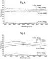
- Figs. 4 and 5show the reflectance curves of a dichroic coating designed to achieve the above reflectance characteristics, for four different incident angles: 20°, 25°, 30° and 75°, with P-polarized and S-polarized light respectively. While the reflectance of the high-angle ray is negligible over the entire relevant spectrum, the rays at off-axis angles of 20°, 25° and 30°, obtain almost constant reflectance of 26%, 29% and 32% respectively, for P-polarized light, and 32%, 28% and 25% respectively, for S-polarized light, over the same spectrum. Evidently, reflectance decreases with the obliquity of the incident rays for P-polarized light and increases for S-polarized light.
- the projection of each surfaceis adjacent to its neighbor.
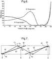
- Fig. 7is an example of a method for coupling the input waves into the substrate.
- Input wavescould, however, also be coupled into the substrate by other optical means, including, but not limited to, folding prisms, fiber optic bundles, diffraction gratings, and other solutions.
- the input waves and the image wavesare located on the same side of the substrate.
- Other configurationsare envisioned in which the input and the image waves could be located on opposite sides of the substrate. It is also possible, in certain applications, to couple the input waves into the substrate through one of the substrate's peripheral sides.
- Fig. 7is a detailed sectional view of an array of selectively reflective surfaces which couple light, trapped inside the substrate, out and into the eye of a viewer.
- the maximal FOVis: FOV max ⁇ 2 T tan ⁇ sur 1 ⁇ d eye R eye .
- the limiting substrate thickness for an FOV of 8°is in the order of 2.8 mm; for FOVs of 15° and 30°, the limiting substrate thickness is 3.7 mm and 5.6 mm, respectively.
- FOVs of 15° and 30°are more favorable values than the limiting thickness of the state-of-the-art solutions discussed above.
- more than two selectively reflecting surfacescan be used.
- the limiting substrate thickness for FOVs of 15° and 30°is approximately 2.4 mm and 3.9 mm, respectively.
- additional reflecting surfacesmay be introduces to, amongst other advantages, reduce the limiting optical thickness further.
- a single partially reflecting surfacecan be sufficient.
- this anglecannot be trapped inside BK7 or other similar materials. It is true that there are flint optical materials with higher refractive indices, which can exceed 1.8, however, the transparency of these materials is usually not high enough for substrate-mode optical elements.
- Another possible solutionis to coat the substrate surfaces not with regular anti-reflection coatings but with angular-sensitive reflecting coatings that trap the entire FOV inside the substrate even for lower angles than the critical angle. It must be noted that even for a non see-through applications, where one of the substrate surfaces can be opaque and hence can be coated with a conventional reflecting surface, the other surface, the one which is next to the eyes of the viewer, should be transparent, at least for the angles of the required external FOV. Therefore, the required reflecting coating should have very high reflectance for the region of angles lower than the critical angle and very high reflectance for the entire FOV of the image.
- LOEIn general, LOE offer several important advantages over alternative compact optics for display applications, which include:
- Fig. 9illustrates an embodiment of the present invention in which the LOE 20 is embedded in an eye-glasses frame 58.
- the display source 4, the collimating lens 6, and the folding lens 60are assembled inside the arm portions 62 of the eye-glasses frame, just next to the edge of the LOE 20.
- the display sourceis an electronic element such as a small CRT, LCD, or OLED
- the driving electronics 64 for the display sourcemight be assembled inside the back portion of the arm 62.
- a power supply and data interface 66is connectable to arm 62 by a lead 68 or other communication means including radio or optical transmission.
- a battery and miniature data link electronicscan be integrated in the eye-glasses frame.
- the embodiment described abovecan serve in both see-through and non-see-through systems.
- opaque layersare located in front of the LOE. It is not necessary to occlude the entire LOE, typically only the active area, where the display is visible needs to be blocked.
- the devicecan ensure that the peripheral vision of the user is maintained, replicating the viewing experience of a computer or a television screen, in which such peripheral vision serves an important cognitive function.
- a variable filtercan be placed in front of the system in such a way that the viewer can control the level of brightness of the light emerging from the external scene.
- This variable filtercould be either a mechanically controlled device such as a folding filter, or two rotating polarizers, an electronically controlled device, or even an automatic device, whereby the transmittance of the filter is determined by the brightness of the external background.
- One method to achieve the required variable transmittance filteris to use electrochromic materials in order to provide electrical control of optical transmittance, wherein materials with electrically controllable optical properties are incorporated into laminated structures.
- an LOEcan be utilized in this embodiment.
- the simplest optionis to use a single element for one eye.
- Another optionis to use an element and a display source for each eye, but with the same image.
- Yet another possibilityis to project two different scenes, one to each eye, in order to create a stereoscopic image.
- attractive implementationsare possible, including 3-dimensional movies, advanced virtual reality, training systems and others.
- Fig. 9is just an example illustrating the simple implementation of the present invention. Since the substrate-guided optical element, constituting the core of the system, is very compact and lightweight, it could be installed in a vast variety of arrangements. Hence, many other embodiments are also possible including a visor, a folding display, a monocle, and many more. This embodiment is designated for applications where the display should be near-to-eye: head-mounted, head-worn or head-carried.
- HUDhead-up displays
- LOE-based HUDpotentially provide the possibilities for a very compact, self-contained HUD, that can be readily installed in confined spaces. It also simplifies the construction and manufacturing of the optical systems related to the HUD and therefore is a potentially suitable for both improving on aerospace HUD's, as well as introducing a compact, inexpensive, consumer version for the automotive industry.
- Fig. 10illustrates a method of materializing an HUD system based on the present invention.
- the light from a display source 4is collimated by a lens 6 to infinity and coupled by the first reflecting surface 16 into substrate 20. After reflection at a second reflecting array (not shown), the optical waves impinge on a third reflecting surfaces 22, which couples the light out into the eyes 24 of the viewer.
- the overall systemcan be very compact and lightweight, of the size of a large postcard having a thickness of a few millimeters.
- the display sourcehaving a volume of a few cubic centimeters, can be attached to one of the corners of the substrate, where an electric wire can transmit the power and data to the system. It is expected that the installation of the presented HUD system will not be more complicated than the installation of a simple commercial audio system. Moreover, since there is no need for an external display source for image projection, the necessity to install components in unsafe places is avoided.
- Fig. 10can be implemented for other applications, in addition to HUD systems for vehicles.
- One possible utilization of these embodimentsis as a flat display for a computer or television.
- the main unique characteristic of such a displayis that the image is not located at the screen plane, but is focused at infinity or to a similarly convenient distance.
- One of the main drawbacks of existing computer displaysis that the user has to focus his eyes at a very close distance of between 40 and 60 cm, while the natural focus of a healthy eye is to infinity.
- Many peoplesuffer from headaches after working for a long duration of time at a computer. Many others who work frequently with computers tend to develop myopia.
- some people, who suffer from both myopia and hyperopianeed special spectacles for work with a computer.
- a flat displaybased on the present invention, could be an appropriate solution for people who suffer from the above-described problems and do not wish to work with a head-mounted display.
- the present inventionallows for a significant reduction in the physical size of the screen. As the image formed by the LOE is larger than the device, it would be possible to implement large screens on smaller frames. This is particularly important for mobile applications such as lap and palm-top computers.
- Yet another possible implementation of this embodimentis as a screen for a personal digital assistance (PDA).
- PDApersonal digital assistance
- the size of the existing conventional screens which are presently used,is under 10 cm. Since the minimal distance where these displays can be read is on the order of 40 cm, the obtainable FOV is under 15°; hence, the information content, especially as far as text is concerned, on these displays is limited.
- a significant improvement in the projected FOVcan be made with the embodiment illustrated in Fig. 10 .
- the imageis focused at infinity, and the screen can be located much closer to the eyes of the viewer.
- TFOVtotal filed-of-view
- another increase in the TFOVmay be achieved. Therefore, a display with an FOV of 40° or larger is feasible.
Landscapes
- Physics & Mathematics (AREA)
- General Physics & Mathematics (AREA)
- Optics & Photonics (AREA)
- Devices For Indicating Variable Information By Combining Individual Elements (AREA)
- Light Guides In General And Applications Therefor (AREA)
- Optical Couplings Of Light Guides (AREA)
- Eye Examination Apparatus (AREA)
- Liquid Crystal (AREA)
Description
- The present invention relates to substrate-guided optical devices, and particularly to devices which include a plurality of reflecting surfaces carried by a common light-transmissive substrate, also referred to as a light-guide.
- The invention can be implemented to advantage in a large number of imaging applications, such as, for example, head-mounted and head-up displays (HMD's and HUD's), cellular phones, compact displays, 3-D displays, compact beam expanders, as well as non-imaging applications such as flat-panel indicators, compact illuminators and scanners.
- One of the important applications for compact optical elements is in HMD's wherein an optical module serves both as an imaging lens and a combiner, in which a two-dimensional display is imaged to infinity and reflected into the eye of an observer. The display can be obtained directly from either a spatial light modulator (SLM) such as a cathode ray tube (CRT), a liquid crystal display (LCD), an organic light emitting diode array (OLED), or a scanning source and similar devices, or indirectly, by means of a relay lens or an optical fiber bundle. The display comprises an array of elements (pixels) imaged to infinity by a collimating lens and transmitted into the eye of the viewer by means of a reflecting or partially reflecting surface acting as a combiner for non-see-through and see-through applications, respectively. Typically, a conventional, free-space optical module is used for these purposes. As the desired field-of-view (FOV) of the system increases, such a conventional optical module becomes larger, heavier and bulkier, and therefore, even for moderate performance devices, impractical. This is a major drawback for all kinds of displays but especially in head-mounted applications, wherein the system must necessarily be as light and as compact as possible.
- The strive for compactness has led to several different complex optical solutions, all of which, on the one hand, are still not sufficiently compact for most practical applications, and on the other hand, suffer major drawbacks in terms of manufacturability, Furthermore, the eye-motion-box (EMB) of the optical viewing angles resulting from these designs is usually very small - typically less than 8 mm. Hence, the performance of the optical system is very sensitive, even to small movements of the optical system relative to the eye of the viewer, and does not allow sufficient pupil motion for conveniently reading text from such displays.
- One such example is disclosed in
WO 03/058320 A1 - Another example for such an optical device is described in
EP 0 399 865 - A further example is the display source disclosed in
WO 98/15868 - The present invention facilitates the structure and fabrication of very compact light-guide optical elements (LOE) for, amongst other applications, head-mounted displays. The invention allows relatively wide FOV7s together with relatively large EMB values. The resulting optical system offers a large, high-quality image, which also accommodates large movements of the eye. The optical system offered by the present invention is particularly advantageous because it is substantially more compact than state-of-the-art implementations and yet it can be readily incorporated, even into optical systems having specialized configurations.
- The invention also enables the construction of improved HUD's. HUD's have become popular and they now play an important role, not only in most modern combat aircrafts, but also in civilian aircrafts, in which HUD systems have become a key component for low-visibility landing operation. Furthermore, there have recently been numerous proposals and designs for HUD7s in automotive applications where they can potentially assist the driver in driving and navigation duties. Nevertheless, state-of-the-art HUD's suffer several significant drawbacks. All HUD7s of the current designs require a display source that must be offset a significant distance from the combiner to ensure that the source illuminates the entire combiner surface. As a result, the combiner-projector HUD system is necessarily bulky and large, and requires considerable installation space, making it inconvenient for installation and, at times, even unsafe to use. The large optical aperture of conventional HUD's also pose a significant optical design challenge, rendering the HUD's with either a compromising performance, or leading to high cost wherever high-performance is required. The chromatic dispersion of high-quality holographic HUD's is of particular concern.
- An important application of the present invention relates to its implementation in a compact HUD, which alleviates the aforementioned drawbacks. In the HUD design of the current invention, the combiner is illuminated with a compact display source that can be attached to the substrate. Hence, the overall system is very compact and can readily be installed in a variety of configurations for a wide range of applications. In addition, the chromatic dispersion of the display is negligible and, as such, can operate with wide spectral sources, including a conventional white-light source. In addition, the present invention expands the image so that the active area of the combiner can be much larger than the area that is actually illuminated by the light source.
- A further application of the present invention is to provide a compact display with a wide FOV for mobile, hand-held application such as cellular phones. In today's wireless Internet-access market, sufficient bandwidth is available for full video transmission. The limiting factor remains the quality of the display within the end-user's device. The mobility requirement restricts the physical size of the displays, and the result is a direct-display with a poor image viewing quality. The present invention enables, a physically very compact display with a very large virtual image. This is a key feature in mobile communications, and especially for mobile Internet access, solving one of the main limitations for its practical implementation. Thereby, the present invention enables the viewing of the digital content of a full format Internet page within a small, hand-held device, such as a cellular phone.
- A broad object of the present invention, therefore, is to alleviate the drawbacks of state-of-the-art compact optical display devices and to provide other optical components and systems having improved performance, according to specific requirements.
- The invention therefore provides an optical device, comprising a light-transmitting substrate having at least two major surfaces parallel to each other and edges; optical means for coupling light waves located in a field-of-view into said light transmitting substrate by internal reflection, and at least one partially reflecting surface located in said light-transmitting substrate which is non-parallel to said major surfaces of the light transmitting substrate, characterized in that at least one of said major surfaces is coated with an angular sensitive reflective coating that traps the entire field-of-view inside the light-transmitting substrate, wherein said major surface has a low reflectance at low incident angles and a high reflectance at high incident angles.
- The invention is described in connection with certain preferred embodiments, with reference to the following illustrative figures so that it may be more fully understood. With specific reference to the figures in detail, it is stressed that the particulars shown are by way of example and for purposes of illustrative discussion of the preferred embodiments of the present invention only, and are presented in the cause of providing what is believed to be the most useful and readily understood description of the principles and conceptual aspects of the invention. In this regard, no attempt is made to show structural details of the invention in more detail than is necessary for a fundamental understanding of the invention. The description taken with the drawings are to serve as direction to those skilled in the art as to how the several forms of the invention may be embodied in practice.
- In the drawings:
Fig. 1 is a side view of a prior art folding optical device;Fig. 2 is a side view of an embodiment of a LOE, in accordance with the present invention;Figs. 3A and 3B illustrate the desired reflectance and transmittance characteristics of selectively reflecting surfaces used in the present invention for two ranges of incident angles;Fig. 4 illustrates the reflectance curves as a function of wavelength for an exemplary dichroic coating for P-polarization;Fig. 5 illustrates a reflectance curve as a function of wavelength for an exemplary dichroic coating for S-polarization;Fig. 6 illustrates the reflectance curves as a function of incident angle for an exemplary dichroic coating;Figs. 7 is a diagram illustrating detailed sectional views of an exemplary array of selectively reflective surfaces;Fig. 8 illustrates the reflectance curves as a function of incident angle for an another dichroic coating;Fig. 9 illustrates an exemplary embodiment of the present invention embedded in a standard eye-glasses frame, andFig. 10 illustrates an exemplary HUD system in accordance with the present invention;Fig. 1 illustrates a conventional folding optics arrangement, wherein thesubstrate 2 is illuminated by adisplay source 4. The display is collimated by acollimating lens 6. The light from thedisplay source 4 is coupled intosubstrate 2 by a first reflectingsurface 8, in such a way that themain ray 10 is parallel to the substrate plane. A second reflectingsurface 12 couples the light out of the substrate and into the eye of aviewer 14. Despite the compactness of this configuration, it suffers significant drawbacks; in particular only a very limited FOV can be affected. As shown inFig. 1 , the maximum allowed off-axis angle inside the substrate is:
- wherein T is the substrate thickness;
- deye is the desired exit-pupil diameter, and
- l is the distance between reflecting
surfaces - With angles higher than αmax the rays are reflected from the substrate surface before arriving at the reflecting
surface 12. Hence, the reflectingsurface 12 will be illuminated at an undesired direction and ghost images appear. - Therefore, the maximum achievable FOV with this configuration is:

Typically the refractive index values lie in the range of 1.5-1.6. - Commonly, the diameter of the eye pupil is 2-6 mm. To accommodate movement or misalignment of the display, a larger exit-pupil diameter is necessary. Taking the minimum desirable value at approximately 8 to 10 mm, the distance between the optical axis of the eye and the side of the head,l, is, typically, between 40 and 80 mm. Consequently, even for a small FOV of 8°, the desired substrate thickness would be of the order of 12 mm.
- Methods have been proposed to overcome the above problem. These include, utilizing a magnifying telescope inside the substrate and non-parallel coupling directions. Even with these solutions, however, and even if only one reflecting surface is considered, the system thickness remains limited by a similar value. The FOV is limited by the diameter of the projection of the
reflective surface 12 on the substrate plane. Mathematically, the maximum achievable FOV, due to this limitation, is expressed as:
- whereinαsur is the angle between the reflecting surface and the normal to the substrate plane, and
- Reye is the distance between the eye of the viewer and the substrate (typically, about 30-40 mm).
- Practically tanαsur cannot be much larger than 1; hence, for the same parameters described above for a FOV of 8°, the required substrate thickness here is on the order of 7 mm, which is an improvement on the previous limit. Nevertheless, as the desired FOV is increased, the substrate thickness increases rapidly. For instance, for desired FOVs of 15° and 30° the substrate limiting thickness is 18 mm or 25 mm, respectively.
- To alleviate the above limitations, the present invention utilizes an array of selectively reflecting surfaces, fabricated within a LOE.
Fig. 2 illustrates a sectional view of an LOE according to the present invention. The first reflectingsurface 16 is illuminated by a collimatedinput plane wave 18, emanating from a display light source (not shown) located behind the device, wherein theplane wave 18 is one of a set of light waves located within a given FOV to be coupled into the LOE. The reflectingsurface 16 reflects the incident light from the source such that the light is trapped inside aplanar substrate 20 by total internal reflection. After several reflections off the surfaces of the substrate, the trapped wave reaches an array of selectively reflectingsurfaces 22, which couple thelight wave 23 out of the substrate into theEMB 24 of a viewer. For avoiding ghost images, theoutput light wave 23 should be a plane wave, otherwise, different rays representing a single point at the display source will arrive at theEMB 24 of the viewer at different incident angles and ghost images that interfere with the primary image will be seen by the viewer. In order to prevent this phenomenon, theoutput light wave 23, and hence theinput wave 18, should be plane waves. That is, the angular deviation between two different rays located on the same light wave should be less thanαres, whereinαres is the angular resolution of the optical device. Usually, for most visual systems,αres is ∼ 1-2 milliradians, but different devices can yield different angular resolutions. - Assuming that the central wave of the source is coupled out of the
substrate 20 in a direction normal to thesubstrate surface 26, and the off-axis angle of the coupled wave inside thesubstrate 20 isαin, then the angle αsur2 between the reflecting surfaces and the substrate plane is:
- As can be seen in
Fig. 2 , the trapped rays arrive at the reflecting surfaces from twodistinct directions directions 28 after an even number of reflections from the substrate surfaces 26, wherein the incident angle βref between the trapped ray and the normal to the reflecting surface is:
- The trapped rays arrive at the reflecting surface from the
second direction 30 after an odd number of reflections from the substrate surfaces 26, where the off-axis angle is α'in = 180°-αin and the incident angle between the trapped ray and the normal to the reflecting surface is:
- In order to prevent undesired reflections and ghost images, the reflectance for one of these two directions should be negligible. The desired discrimination between the two incident directions can be achieved if one angle is significantly smaller then the other one. It is possible to provide a coating with very low reflectance at high incident angles and a high reflectance for low incident angles. This property can be exploited to prevent undesired reflections and ghost images by eliminating the reflectance in one of the two directions. For example choosing βref∼ 25° from Equations (5) and (6) it can be calculated that:

- If now a reflecting surface is determined for which β'ref is not reflected but βref is, the desired condition is achieved.
Fig. 3A and 3B illustrate the desired reflectance behavior of selectively reflecting surfaces. While the ray 32 (Fig. 3A ), having an off-axis angle of βref∼ 25°, is partially reflected and is coupled out of thesubstrate 34, the ray 36 (Fig. 3B ), which arrives at an off-axis angle of β'ref∼ 75° to the reflecting surface (which is equivalent to β'ref∼ 105°), is transmitted through the reflectingsurface 34 without any notable reflection. Figs. 4 and 5 show the reflectance curves of a dichroic coating designed to achieve the above reflectance characteristics, for four different incident angles: 20°, 25°, 30° and 75°, with P-polarized and S-polarized light respectively. While the reflectance of the high-angle ray is negligible over the entire relevant spectrum, the rays at off-axis angles of 20°, 25° and 30°, obtain almost constant reflectance of 26%, 29% and 32% respectively, for P-polarized light, and 32%, 28% and 25% respectively, for S-polarized light, over the same spectrum. Evidently, reflectance decreases with the obliquity of the incident rays for P-polarized light and increases for S-polarized light.Fig. 6 illustrates the reflectance curves of the same dichroic coating, as a function of the incident angle for both polarizations at wavelength λ=550 nm. There are two significant regions in this graph: between 65° and 80° where the reflectance is very low, and between 15° and 40° where the reflectance changes monotonically with decreasing incident angles (increasing for P-polarized light and decreasing for S-polarized light). Hence, as long as one can ensure that the entire angular spectrum of β'ref, where very low reflections are desired, will be located inside the first region, while the entire angular spectrum of βref, where higher reflections are required, will be located inside the second region, for a given FOV, one can ensure the reflection of only one substrate mode into the eye of the viewer and a ghost-free image.- There are some differences between the behaviors of the two polarizations. The main differences are that the region of high angles, where the reflectance is very low, is much narrower for the S-polarization and that it is much more difficult to achieve a constant reflectance for a given angle over the entire spectral bandwidth for the S-polarized light than for the P-polarized light. It is therefore preferable to design the LOE only for the P-polarized light. This would be satisfactory for a system using a polarized display source, such as an LCD, or for a system where the output brightness is not crucial and the S-polarized light can be filtered out. However, for an unpolarized display source, like a CRT or an OLED, or for a system where the brightness is critical, S-polarized light cannot be neglected and it must be taken into account during the design procedure. Another difference is that the monotonic behavior of the S-polarized light at the angular spectrum of βref, where higher reflections are required, is opposite to that of the P-polarized light, that is, the reflectance for the S-polarized light increases with the obliquity of the incident rays. This contradictory behavior of the two polarizations at the angular spectrum of βref could be utilized during the optical design of the system to achieve the desired reflectance of the overall light according to the specific requirements of each system.
- Assuming that the coupled wave illuminates the entire area of the reflecting surface, after reflection from the
surface 16, it illuminates an area of2S1 =2T tan(α) on the substrate surface. On the other hand, the projection of areflection surface 22 on the substrate plane, isS2 =T tan(αsur2). To avoid either overlapping or gaps between the reflecting surfaces, the projection of each surface is adjacent to its neighbor. Hence, the number N of reflectingsurfaces 22 through which each coupled ray passes during one cycle (i.e., between two reflections from the same surface of the substrate) is:
- In this example, where αsur2 = 25° and αsur1 = 25°, the solution isN = 2; that is, each ray passes through two different surfaces during one cycle.
- The embodiment described above with regard to
Fig. 7 is an example of a method for coupling the input waves into the substrate. Input waves could, however, also be coupled into the substrate by other optical means, including, but not limited to, folding prisms, fiber optic bundles, diffraction gratings, and other solutions. - Also, in the example illustrated in
Fig. 2 , the input waves and the image waves are located on the same side of the substrate. Other configurations are envisioned in which the input and the image waves could be located on opposite sides of the substrate. It is also possible, in certain applications, to couple the input waves into the substrate through one of the substrate's peripheral sides. Fig. 7 is a detailed sectional view of an array of selectively reflective surfaces which couple light, trapped inside the substrate, out and into the eye of a viewer. As can be seen, in each cycle the coupled ray passes through reflectingsurfaces 43, at an angle of α'in = 130°, whereby the angle between the ray and the normal to the reflecting surfaces is ∼75°. The reflections from these surfaces are negligible. In addition, the ray passes twice through the reflectingsurface 44, in each cycle, at an angle of αin = 50°, where the incident angle is 25°. Part of the energy of the ray is coupled out of the substrate. Assuming that one array of two selectively reflectingsurfaces 22 is used to couple the light onto the eye of a viewer, the maximal FOV is:
- Hence, for the same parameters of the examples above, the limiting substrate thickness for an FOV of 8° is in the order of 2.8 mm; for FOVs of 15° and 30°, the limiting substrate thickness is 3.7 mm and 5.6 mm, respectively. These are more favorable values than the limiting thickness of the state-of-the-art solutions discussed above. Moreover, more than two selectively reflecting surfaces can be used. For example, for three selectively reflecting
surfaces 22, the limiting substrate thickness for FOVs of 15° and 30° is approximately 2.4 mm and 3.9 mm, respectively. Similarly additional reflecting surfaces may be introduces to, amongst other advantages, reduce the limiting optical thickness further. - For configuration where a relatively small FOV is required, a single partially reflecting surface can be sufficient. For example, for a system with the following parameters:Reye = 25 mm ; αsur = 72° andT= 5 mm, a moderate FOV of 17° can be achieved even with a
single reflecting surface 22. Part of the rays will cross thesurface 22 several times before being coupled out into the desired direction. Since the minimal propagation angle inside the substrate to achieve the total-internal reflection condition for BK7 material or similar is αin(min) = 42°, the propagation direction of the central angle of the FOV is αin(cen) = 48°. Consequently, the projected image is not normal to the surface but is rather inclined to 12° off-axis. Nevertheless, for many applications this is acceptable. - Unfortunately, this solution is not always feasible. For many other applications there is a constraint that the projected image should be normal to the substrate surface. Another problem, which is associated with the total internal reflection condition, is the maximal FOV of the image that can be trapped inside the substrate. Unfortunately, it is very difficult to achieve very low reflectance for off-axis angles exceeding 82°. Assuming that the required FOV angle inside the substrate is αFOV, the maximal incident angle between the central wave and the normal to the reflecting surface is

- Assuming an external FOV of 30°, which corresponds toαFOV ∼20° inside the substrate, yieldsβ'ref = 72°. Inserting this value into Eq. (6) yields αin=48°, and hence the minimal required angle of the trapped wave is

- Clearly, this angle cannot be trapped inside BK7 or other similar materials. It is true that there are flint optical materials with higher refractive indices, which can exceed 1.8, however, the transparency of these materials is usually not high enough for substrate-mode optical elements. Another possible solution is to coat the substrate surfaces not with regular anti-reflection coatings but with angular-sensitive reflecting coatings that trap the entire FOV inside the substrate even for lower angles than the critical angle. It must be noted that even for a non see-through applications, where one of the substrate surfaces can be opaque and hence can be coated with a conventional reflecting surface, the other surface, the one which is next to the eyes of the viewer, should be transparent, at least for the angles of the required external FOV. Therefore, the required reflecting coating should have very high reflectance for the region of angles lower than the critical angle and very high reflectance for the entire FOV of the image.
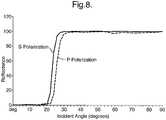
Fig. 8 shows the reflectance curves of a dichroic coating designed to achieve the above reflectance characteristics, as a function of the incident angle, for both polarizations at the wavelength λ=550 nm, where the angle is measured in air. Evidently, there are two significant regions in this graph: between 30° and 90° (equivalent to 20° - 42° inside the substrate) where the reflectance is very high; and between 0° and 22° (equivalent to 0° - 15° inside the substrate) where the reflectance is very low. Hence, as long as one can ensure that the entire angular spectrum of αin, where very high reflections are desired, will be located inside the first region, while the entire angular spectrum of exterior FOV, where essentially zero reflections are required, will be located inside the second region, for a given FOV, one can ensure that the entire FOV will be trapped inside the substrate by internal reflections and that the viewer can see the whole image. It is important to note that since the fabrication process of the LOE usually involves cementing optical elements and since the required angular-sensitive reflecting coating is applied to the substrate surface only after the LOE body is complete, it is not possible to utilize the conventional hot-coating procedures that may damage the cemented areas. Fortunately, novel thin-film technologies, as ion-assisted coating procedures, can also be used for cold processing. Eliminating the need to heat parts allows cemented parts, such as LOEs, to be safely coated.- In general, LOE offer several important advantages over alternative compact optics for display applications, which include:
- 1) The input display source can be located very close to the substrate, so that the overall optical system is very compact and lightweight, offering an unparalleled form-factor.
- 2) In contrast to other compact display configurations, the present invention offers flexibility as to location of the input display source relative to the eyepiece. This flexibility, combined with the ability to locate the source close to the expanding substrate, alleviates the need to use an off-axis optical configuration that is common to other display systems. In addition, since the input aperture of the LOE is much smaller than the active area of the output aperture, the numerical aperture of the
collimating lens 6 is much smaller than required for a comparable conventional imaging system. Consequently a significantly more convenient optical system can be implemented and the many difficulties associated with off-axis optics and high numerical-aperture lenses, such as field or chromatic aberrations can be compensated for relatively easily and efficiently. - 3) The reflectance coefficients of the selectively reflective surfaces in the present invention are essentially identical over the entire relevant spectrum. Hence, both monochromatic and polychromatic, light sources may be used as display sources. The LOE has a negligible wavelength-dependence ensuring high-quality color displays with high resolutions.
- 4) Since each point from the input display is transformed into a plane wave that is reflected into the eye of the viewer from a large part of the reflecting array, the tolerances on the exact location of the eye can be significantly relaxed. As such, the viewer can see the entire FOV, and the EMB can be significantly larger than in other compact display configurations.
- 5) Since a large part of the intensity from the display source is coupled into the substrate, and since a large portion of this coupled energy is "recycled" and coupled out into the eye of the viewer, a display of comparatively high brightness can be achieved even with display sources with low power consumption.
Fig. 9 illustrates an embodiment of the present invention in which theLOE 20 is embedded in an eye-glasses frame 58. Thedisplay source 4, thecollimating lens 6, and thefolding lens 60 are assembled inside thearm portions 62 of the eye-glasses frame, just next to the edge of theLOE 20. For a case in which the display source is an electronic element such as a small CRT, LCD, or OLED, the drivingelectronics 64 for the display source might be assembled inside the back portion of thearm 62. A power supply anddata interface 66 is connectable toarm 62 by a lead 68 or other communication means including radio or optical transmission. Alternatively, a battery and miniature data link electronics can be integrated in the eye-glasses frame.- The embodiment described above can serve in both see-through and non-see-through systems. In the latter case opaque layers are located in front of the LOE. It is not necessary to occlude the entire LOE, typically only the active area, where the display is visible needs to be blocked. As such, the device can ensure that the peripheral vision of the user is maintained, replicating the viewing experience of a computer or a television screen, in which such peripheral vision serves an important cognitive function. Alternatively, a variable filter can be placed in front of the system in such a way that the viewer can control the level of brightness of the light emerging from the external scene. This variable filter could be either a mechanically controlled device such as a folding filter, or two rotating polarizers, an electronically controlled device, or even an automatic device, whereby the transmittance of the filter is determined by the brightness of the external background. One method to achieve the required variable transmittance filter is to use electrochromic materials in order to provide electrical control of optical transmittance, wherein materials with electrically controllable optical properties are incorporated into laminated structures.
- There are some alternatives as to the precise way in which an LOE can be utilized in this embodiment. The simplest option is to use a single element for one eye. Another option is to use an element and a display source for each eye, but with the same image. Alternatively it is possible to project two different parts of the same image, with some overlap between the two eyes, enabling a wider FOV. Yet another possibility is to project two different scenes, one to each eye, in order to create a stereoscopic image. With this alternative, attractive implementations are possible, including 3-dimensional movies, advanced virtual reality, training systems and others.
- The embodiment of
Fig. 9 is just an example illustrating the simple implementation of the present invention. Since the substrate-guided optical element, constituting the core of the system, is very compact and lightweight, it could be installed in a vast variety of arrangements. Hence, many other embodiments are also possible including a visor, a folding display, a monocle, and many more. This embodiment is designated for applications where the display should be near-to-eye: head-mounted, head-worn or head-carried. - The embodiment described above is a mono-ocular optical system, that is, the image is projected onto a single eye. There are, however, applications, such as head-up displays (HUD), wherein it is desired to project an image onto both eyes. Until recently, HUD systems have been used mainly in advanced combat and civilian aircraft. There have been numerous proposals and designs, of late, to install a HUD in front of a car driver in order to assist in driving navigation or to project a thermal image into his eyes during low-visibility conditions. Current aerospace HUD systems are very expensive, the price of a single unit being in the order of hundreds of thousands of dollars. In addition, the existing systems are very large, heavy, and bulky, and are too cumbersome for installation in a small aircraft let alone a car. LOE-based HUD potentially provide the possibilities for a very compact, self-contained HUD, that can be readily installed in confined spaces. It also simplifies the construction and manufacturing of the optical systems related to the HUD and therefore is a potentially suitable for both improving on aerospace HUD's, as well as introducing a compact, inexpensive, consumer version for the automotive industry.
Fig. 10 illustrates a method of materializing an HUD system based on the present invention. The light from adisplay source 4 is collimated by alens 6 to infinity and coupled by the first reflectingsurface 16 intosubstrate 20. After reflection at a second reflecting array (not shown), the optical waves impinge on a third reflectingsurfaces 22, which couples the light out into theeyes 24 of the viewer. The overall system can be very compact and lightweight, of the size of a large postcard having a thickness of a few millimeters. The display source, having a volume of a few cubic centimeters, can be attached to one of the corners of the substrate, where an electric wire can transmit the power and data to the system. It is expected that the installation of the presented HUD system will not be more complicated than the installation of a simple commercial audio system. Moreover, since there is no need for an external display source for image projection, the necessity to install components in unsafe places is avoided.- The embodiments illustrated in
Fig. 10 can be implemented for other applications, in addition to HUD systems for vehicles. One possible utilization of these embodiments is as a flat display for a computer or television. The main unique characteristic of such a display is that the image is not located at the screen plane, but is focused at infinity or to a similarly convenient distance. One of the main drawbacks of existing computer displays is that the user has to focus his eyes at a very close distance of between 40 and 60 cm, while the natural focus of a healthy eye is to infinity. Many people suffer from headaches after working for a long duration of time at a computer. Many others who work frequently with computers tend to develop myopia. In addition, some people, who suffer from both myopia and hyperopia, need special spectacles for work with a computer. A flat display, based on the present invention, could be an appropriate solution for people who suffer from the above-described problems and do not wish to work with a head-mounted display. Furthermore, the present invention allows for a significant reduction in the physical size of the screen. As the image formed by the LOE is larger than the device, it would be possible to implement large screens on smaller frames. This is particularly important for mobile applications such as lap and palm-top computers. - Yet another possible implementation of this embodiment is as a screen for a personal digital assistance (PDA). The size of the existing conventional screens which are presently used, is under 10 cm. Since the minimal distance where these displays can be read is on the order of 40 cm, the obtainable FOV is under 15°; hence, the information content, especially as far as text is concerned, on these displays is limited. A significant improvement in the projected FOV can be made with the embodiment illustrated in
Fig. 10 . The image is focused at infinity, and the screen can be located much closer to the eyes of the viewer. In addition, since each eye sees a different part of the total filed-of-view (TFOV), with an overlap at its center, another increase in the TFOV may be achieved. Therefore, a display with an FOV of 40° or larger is feasible. - It will be evident to those skilled in the art that the invention is not limited to the details of the foregoing illustrated embodiments and that the present invention may be embodied in other specific forms without departing from the spirit or essential attributes thereof. The present embodiments are therefore to be considered in all respects as illustrative and not restrictive, the scope of the invention being indicated by the appended claims rather than by the foregoing description, and all changes which come within the meaning and range of equivalency of the claims are therefore intended to be embraced therein.


Claims (16)
- An optical device, comprising a light-transmitting substrate (20) having at least two major surfaces (26) parallel to each other and edges;
optical means (16) for coupling light waves located in a field-of-view into said light-transmitting substrate (20) by internal reflection, and
at least one partially reflecting surface (22) located in said light-transmitting substrate (20) which is non-parallel to said major surfaces (26) of said light-transmitting substrate (20),
characterized in that at least one of said major surfaces (26) is coated with an angular sensitive reflective coating that traps the entire field-of-view inside said light-transmitting substrate (20), wherein said major surface (26) has a low reflectance at low incident angles and a high reflectance at high incident angles. - The optical device according to claim 1,characterized in that said angular sensitive reflective coating has a high reflectance for a first range of high incident angles of light impinging on said major surface (26) coated with said angular sensitive reflective coating, and a low reflectance for a second range of low incident angles of light impinging on said major surface (26) coated with said angular sensitive reflective coating.
- The optical device according to claim 1, wherein said major surface (26) has a negligible reflection for one part of the angular spectrum and a significant reflection for other parts of the angular spectrum.
- The optical device according to claim 1, wherein said angular sensitive coating causes the entire field-of-view to be trapped inside said light-transmitting substrate (20) by internal reflections.
- The optical device according to claim 1, wherein said at least one partially reflecting surface (22) couples light trapped by internal reflection out of said light-transmitting substrate (20).
- The optical device according to claim 1, wherein said angular sensitive coating causes the entire field-of-view to exit said light-transmitting substrate (20) at a predetermined location for reaching at least one eye (14) of an observer.
- The optical device according to claim 1, wherein said angular sensitive coating is formed by utilizing an ion-assisted coating procedure.
- The optical device according to claim 1, further comprising a display light source (4).
- The optical device according to claim 8, wherein said display light source (4) is a liquid crystal display.
- The optical device according to claim 8, wherein said display light source (4) is an organic light emitting diode display.
- The optical device according to claim 1, wherein said light-transmitting substrate (20) is partially transparent, to enable see-through operation.
- The optical device according to claim 1, further comprising an opaque surface located on or in said light-transmitting substrate (20), so as to block the entrance of light traversing said light-transmitting-substrate (20) from an external scene.
- The optical device according to claim 1, further comprising a variable transmittance surface located so as to attenuate the entrance of light traversing said light-transmitting substrate (20), for controlling brightness of light passing through said device from an external scene.
- The optical device according to claim 13, wherein the transmittance of said variable transmittance surface is determined according to the brightness of light directed to traverse said light-transmitting substrate (20).
- The optical device according to claim 1, wherein said device is mounted in an eyeglasses frame.
- The optical device according to claim 1, wherein said device is located in a head-up-display.
Priority Applications (1)
| Application Number | Priority Date | Filing Date | Title |
|---|---|---|---|
| EP17163372.0AEP3223060B1 (en) | 2003-09-10 | 2004-09-09 | Substrate-guided optical devices |
Applications Claiming Priority (2)
| Application Number | Priority Date | Filing Date | Title |
|---|---|---|---|
| IL157837AIL157837A (en) | 2003-09-10 | 2003-09-10 | Substrate-guided optical device particularly for three-dimensional displays |
| PCT/IL2004/000813WO2005024491A1 (en) | 2003-09-10 | 2004-09-09 | Substrate-guided optical devices |
Related Child Applications (1)
| Application Number | Title | Priority Date | Filing Date |
|---|---|---|---|
| EP17163372.0ADivisionEP3223060B1 (en) | 2003-09-10 | 2004-09-09 | Substrate-guided optical devices |
Publications (2)
| Publication Number | Publication Date |
|---|---|
| EP1664898A1 EP1664898A1 (en) | 2006-06-07 |
| EP1664898B1true EP1664898B1 (en) | 2017-03-29 |
Family
ID=34259910
Family Applications (3)
| Application Number | Title | Priority Date | Filing Date |
|---|---|---|---|
| EP04770484.6AExpired - LifetimeEP1664898B1 (en) | 2003-09-10 | 2004-09-09 | Substrate-guided optical devices |
| EP04770485.3AExpired - LifetimeEP1664899B1 (en) | 2003-09-10 | 2004-09-09 | Substrate-guided optical devices |
| EP17163372.0AExpired - LifetimeEP3223060B1 (en) | 2003-09-10 | 2004-09-09 | Substrate-guided optical devices |
Family Applications After (2)
| Application Number | Title | Priority Date | Filing Date |
|---|---|---|---|
| EP04770485.3AExpired - LifetimeEP1664899B1 (en) | 2003-09-10 | 2004-09-09 | Substrate-guided optical devices |
| EP17163372.0AExpired - LifetimeEP3223060B1 (en) | 2003-09-10 | 2004-09-09 | Substrate-guided optical devices |
Country Status (12)
| Country | Link |
|---|---|
| US (3) | US7391573B2 (en) |
| EP (3) | EP1664898B1 (en) |
| JP (2) | JP4628360B2 (en) |
| KR (2) | KR101065069B1 (en) |
| CN (2) | CN100529837C (en) |
| AU (2) | AU2004271393B2 (en) |
| BR (1) | BRPI0413948B1 (en) |
| CA (2) | CA2538375C (en) |
| IL (1) | IL157837A (en) |
| RU (1) | RU2358301C2 (en) |
| WO (2) | WO2005024491A1 (en) |
| ZA (1) | ZA200602016B (en) |
Families Citing this family (415)
| Publication number | Priority date | Publication date | Assignee | Title |
|---|---|---|---|---|
| JP4605152B2 (en)* | 2004-03-12 | 2011-01-05 | 株式会社ニコン | Image display optical system and image display apparatus |
| IL166799A (en) | 2005-02-10 | 2014-09-30 | Lumus Ltd | Substrate-guided optical device utilizing beam splitters |
| US10073264B2 (en) | 2007-08-03 | 2018-09-11 | Lumus Ltd. | Substrate-guide optical device |
| US7724443B2 (en)* | 2005-02-10 | 2010-05-25 | Lumus Ltd. | Substrate-guided optical device utilizing thin transparent layer |
| US10261321B2 (en)* | 2005-11-08 | 2019-04-16 | Lumus Ltd. | Polarizing optical system |
| GB0522968D0 (en) | 2005-11-11 | 2005-12-21 | Popovich Milan M | Holographic illumination device |
| EP1952189B1 (en)* | 2005-11-21 | 2016-06-01 | Microvision, Inc. | Display with image-guiding substrate |
| IL174170A (en)* | 2006-03-08 | 2015-02-26 | Abraham Aharoni | Device and method for binocular alignment |
| GB0718706D0 (en) | 2007-09-25 | 2007-11-07 | Creative Physics Ltd | Method and apparatus for reducing laser speckle |
| IL177618A (en) | 2006-08-22 | 2015-02-26 | Lumus Ltd | Substrate- guided optical device |
| US8643948B2 (en) | 2007-04-22 | 2014-02-04 | Lumus Ltd. | Collimating optical device and system |
| US7589901B2 (en)* | 2007-07-10 | 2009-09-15 | Microvision, Inc. | Substrate-guided relays for use with scanned beam light sources |
| FR2925172B1 (en)* | 2007-12-13 | 2010-08-20 | Optinvent | OPTICAL GUIDE AND OPTICAL SYSTEM OF OCULAR VISION. |
| FR2925171B1 (en) | 2007-12-13 | 2010-04-16 | Optinvent | OPTICAL GUIDE AND OPTICAL SYSTEM OF EYE VISION |
| FR2929720B1 (en)* | 2008-04-03 | 2010-11-12 | Optinvent | CATADIOPTRIC COLLIMATOR |
| US7854523B2 (en)* | 2008-08-26 | 2010-12-21 | Microvision, Inc. | Optical relay for compact head up display |
| DE102008049407A1 (en)* | 2008-09-29 | 2010-04-01 | Carl Zeiss Ag | Display device and display method |
| JP4636164B2 (en) | 2008-10-23 | 2011-02-23 | ソニー株式会社 | Head-mounted display |
| FR2938934B1 (en) | 2008-11-25 | 2017-07-07 | Essilor Int - Cie Generale D'optique | GLASSES OF EYEWEAR PROVIDING OPHTHALMIC VISION AND ADDITIONAL VISION |
| JP5389493B2 (en)* | 2009-03-25 | 2014-01-15 | オリンパス株式会社 | Glasses-mounted image display device |
| US8059342B2 (en)* | 2009-04-03 | 2011-11-15 | Vuzix Corporation | Beam segmentor for enlarging viewing aperture of microdisplay |
| ES2621820T3 (en)* | 2009-04-20 | 2017-07-05 | Bae Systems Plc | Surface relief grid in an optical waveguide with a reflective surface and a surface-adapted dielectric layer |
| EP2422228B1 (en)* | 2009-04-20 | 2023-01-25 | BAE Systems PLC | Improvements in optical waveguides |
| US8441733B2 (en)* | 2009-04-24 | 2013-05-14 | David Kessler | Pupil-expanded volumetric display |
| US11726332B2 (en) | 2009-04-27 | 2023-08-15 | Digilens Inc. | Diffractive projection apparatus |
| US9335604B2 (en) | 2013-12-11 | 2016-05-10 | Milan Momcilo Popovich | Holographic waveguide display |
| JP5402293B2 (en)* | 2009-06-22 | 2014-01-29 | ソニー株式会社 | Head-mounted display and image display method in head-mounted display |
| US20120224062A1 (en)* | 2009-08-07 | 2012-09-06 | Light Blue Optics Ltd | Head up displays |
| JP2011070049A (en)* | 2009-09-28 | 2011-04-07 | Brother Industries Ltd | Head-mounted display |
| US8233204B1 (en) | 2009-09-30 | 2012-07-31 | Rockwell Collins, Inc. | Optical displays |
| US10795160B1 (en) | 2014-09-25 | 2020-10-06 | Rockwell Collins, Inc. | Systems for and methods of using fold gratings for dual axis expansion |
| US11300795B1 (en) | 2009-09-30 | 2022-04-12 | Digilens Inc. | Systems for and methods of using fold gratings coordinated with output couplers for dual axis expansion |
| US11320571B2 (en) | 2012-11-16 | 2022-05-03 | Rockwell Collins, Inc. | Transparent waveguide display providing upper and lower fields of view with uniform light extraction |
| US20200057353A1 (en) | 2009-10-09 | 2020-02-20 | Digilens Inc. | Compact Edge Illuminated Diffractive Display |
| US11204540B2 (en) | 2009-10-09 | 2021-12-21 | Digilens Inc. | Diffractive waveguide providing a retinal image |
| US8659826B1 (en) | 2010-02-04 | 2014-02-25 | Rockwell Collins, Inc. | Worn display system and method without requiring real time tracking for boresight precision |
| US20150309316A1 (en) | 2011-04-06 | 2015-10-29 | Microsoft Technology Licensing, Llc | Ar glasses with predictive control of external device based on event input |
| US8472120B2 (en) | 2010-02-28 | 2013-06-25 | Osterhout Group, Inc. | See-through near-eye display glasses with a small scale image source |
| US9134534B2 (en) | 2010-02-28 | 2015-09-15 | Microsoft Technology Licensing, Llc | See-through near-eye display glasses including a modular image source |
| US9128281B2 (en) | 2010-09-14 | 2015-09-08 | Microsoft Technology Licensing, Llc | Eyepiece with uniformly illuminated reflective display |
| WO2011106797A1 (en) | 2010-02-28 | 2011-09-01 | Osterhout Group, Inc. | Projection triggering through an external marker in an augmented reality eyepiece |
| US20120249797A1 (en) | 2010-02-28 | 2012-10-04 | Osterhout Group, Inc. | Head-worn adaptive display |
| US9341843B2 (en) | 2010-02-28 | 2016-05-17 | Microsoft Technology Licensing, Llc | See-through near-eye display glasses with a small scale image source |
| US8477425B2 (en) | 2010-02-28 | 2013-07-02 | Osterhout Group, Inc. | See-through near-eye display glasses including a partially reflective, partially transmitting optical element |
| US8467133B2 (en) | 2010-02-28 | 2013-06-18 | Osterhout Group, Inc. | See-through display with an optical assembly including a wedge-shaped illumination system |
| US8482859B2 (en) | 2010-02-28 | 2013-07-09 | Osterhout Group, Inc. | See-through near-eye display glasses wherein image light is transmitted to and reflected from an optically flat film |
| US9091851B2 (en) | 2010-02-28 | 2015-07-28 | Microsoft Technology Licensing, Llc | Light control in head mounted displays |
| US10180572B2 (en) | 2010-02-28 | 2019-01-15 | Microsoft Technology Licensing, Llc | AR glasses with event and user action control of external applications |
| US9229227B2 (en) | 2010-02-28 | 2016-01-05 | Microsoft Technology Licensing, Llc | See-through near-eye display glasses with a light transmissive wedge shaped illumination system |
| US9223134B2 (en) | 2010-02-28 | 2015-12-29 | Microsoft Technology Licensing, Llc | Optical imperfections in a light transmissive illumination system for see-through near-eye display glasses |
| US9182596B2 (en) | 2010-02-28 | 2015-11-10 | Microsoft Technology Licensing, Llc | See-through near-eye display glasses with the optical assembly including absorptive polarizers or anti-reflective coatings to reduce stray light |
| US9129295B2 (en) | 2010-02-28 | 2015-09-08 | Microsoft Technology Licensing, Llc | See-through near-eye display glasses with a fast response photochromic film system for quick transition from dark to clear |
| US8488246B2 (en) | 2010-02-28 | 2013-07-16 | Osterhout Group, Inc. | See-through near-eye display glasses including a curved polarizing film in the image source, a partially reflective, partially transmitting optical element and an optically flat film |
| US9285589B2 (en) | 2010-02-28 | 2016-03-15 | Microsoft Technology Licensing, Llc | AR glasses with event and sensor triggered control of AR eyepiece applications |
| US9097890B2 (en) | 2010-02-28 | 2015-08-04 | Microsoft Technology Licensing, Llc | Grating in a light transmissive illumination system for see-through near-eye display glasses |
| US9759917B2 (en) | 2010-02-28 | 2017-09-12 | Microsoft Technology Licensing, Llc | AR glasses with event and sensor triggered AR eyepiece interface to external devices |
| US9366862B2 (en) | 2010-02-28 | 2016-06-14 | Microsoft Technology Licensing, Llc | System and method for delivering content to a group of see-through near eye display eyepieces |
| US9097891B2 (en) | 2010-02-28 | 2015-08-04 | Microsoft Technology Licensing, Llc | See-through near-eye display glasses including an auto-brightness control for the display brightness based on the brightness in the environment |
| JP5712537B2 (en)* | 2010-09-24 | 2015-05-07 | セイコーエプソン株式会社 | Virtual image display device |
| US9632315B2 (en) | 2010-10-21 | 2017-04-25 | Lockheed Martin Corporation | Head-mounted display apparatus employing one or more fresnel lenses |
| US10359545B2 (en) | 2010-10-21 | 2019-07-23 | Lockheed Martin Corporation | Fresnel lens with reduced draft facet visibility |
| US8625200B2 (en) | 2010-10-21 | 2014-01-07 | Lockheed Martin Corporation | Head-mounted display apparatus employing one or more reflective optical surfaces |
| US8781794B2 (en) | 2010-10-21 | 2014-07-15 | Lockheed Martin Corporation | Methods and systems for creating free space reflective optical surfaces |
| US8503087B1 (en) | 2010-11-02 | 2013-08-06 | Google Inc. | Structured optical surface |
| US8582209B1 (en) | 2010-11-03 | 2013-11-12 | Google Inc. | Curved near-to-eye display |
| US8743464B1 (en) | 2010-11-03 | 2014-06-03 | Google Inc. | Waveguide with embedded mirrors |
| US9292973B2 (en) | 2010-11-08 | 2016-03-22 | Microsoft Technology Licensing, Llc | Automatic variable virtual focus for augmented reality displays |
| US9304319B2 (en) | 2010-11-18 | 2016-04-05 | Microsoft Technology Licensing, Llc | Automatic focus improvement for augmented reality displays |
| AU2011343660A1 (en) | 2010-12-16 | 2013-07-04 | Lockheed Martin Corporation | Collimating display with pixel lenses |
| US9690099B2 (en)* | 2010-12-17 | 2017-06-27 | Microsoft Technology Licensing, Llc | Optimized focal area for augmented reality displays |
| US8576143B1 (en) | 2010-12-20 | 2013-11-05 | Google Inc. | Head mounted display with deformation sensors |
| US8531773B2 (en) | 2011-01-10 | 2013-09-10 | Microvision, Inc. | Substrate guided relay having a homogenizing layer |
| US8391668B2 (en) | 2011-01-13 | 2013-03-05 | Microvision, Inc. | Substrate guided relay having an absorbing edge to reduce alignment constraints |
| JP5633406B2 (en) | 2011-02-04 | 2014-12-03 | セイコーエプソン株式会社 | Virtual image display device |
| JP2012163656A (en) | 2011-02-04 | 2012-08-30 | Seiko Epson Corp | Virtual image display device |
| JP5720290B2 (en) | 2011-02-16 | 2015-05-20 | セイコーエプソン株式会社 | Virtual image display device |
| US8189263B1 (en) | 2011-04-01 | 2012-05-29 | Google Inc. | Image waveguide with mirror arrays |
| WO2012136970A1 (en) | 2011-04-07 | 2012-10-11 | Milan Momcilo Popovich | Laser despeckler based on angular diversity |
| US8666212B1 (en) | 2011-04-28 | 2014-03-04 | Google Inc. | Head mounted display using a fused fiber bundle |
| US9329388B1 (en) | 2011-04-28 | 2016-05-03 | Google Inc. | Heads-up display for a large transparent substrate |
| US8699842B2 (en) | 2011-05-27 | 2014-04-15 | Google Inc. | Image relay waveguide and method of producing same |
| JP2012252091A (en)* | 2011-06-01 | 2012-12-20 | Sony Corp | Display apparatus |
| US8817379B2 (en) | 2011-07-12 | 2014-08-26 | Google Inc. | Whole image scanning mirror display system |
| US8471967B2 (en) | 2011-07-15 | 2013-06-25 | Google Inc. | Eyepiece for near-to-eye display with multi-reflectors |
| US8508851B2 (en) | 2011-07-20 | 2013-08-13 | Google Inc. | Compact see-through display system |
| US8767305B2 (en) | 2011-08-02 | 2014-07-01 | Google Inc. | Method and apparatus for a near-to-eye display |
| US8294994B1 (en) | 2011-08-12 | 2012-10-23 | Google Inc. | Image waveguide having non-parallel surfaces |
| US8760762B1 (en) | 2011-08-12 | 2014-06-24 | Google Inc. | Image waveguide utilizing two mirrored or polarized surfaces |
| US8472119B1 (en) | 2011-08-12 | 2013-06-25 | Google Inc. | Image waveguide having a bend |
| US8823740B1 (en) | 2011-08-15 | 2014-09-02 | Google Inc. | Display system |
| WO2016020630A2 (en) | 2014-08-08 | 2016-02-11 | Milan Momcilo Popovich | Waveguide laser illuminator incorporating a despeckler |
| EP2995986B1 (en) | 2011-08-24 | 2017-04-12 | Rockwell Collins, Inc. | Data display |
| US10670876B2 (en) | 2011-08-24 | 2020-06-02 | Digilens Inc. | Waveguide laser illuminator incorporating a despeckler |
| CA2750287C (en) | 2011-08-29 | 2012-07-03 | Microsoft Corporation | Gaze detection in a see-through, near-eye, mixed reality display |
| JP6144681B2 (en) | 2011-08-30 | 2017-06-07 | マイクロソフト テクノロジー ライセンシング,エルエルシー | Head mounted display with iris scan profiling function |
| US8786686B1 (en) | 2011-09-16 | 2014-07-22 | Google Inc. | Head mounted display eyepiece with integrated depth sensing |
| US9013793B2 (en) | 2011-09-21 | 2015-04-21 | Google Inc. | Lightweight eyepiece for head mounted display |
| US8941560B2 (en) | 2011-09-21 | 2015-01-27 | Google Inc. | Wearable computer with superimposed controls and instructions for external device |
| US8767306B1 (en) | 2011-09-22 | 2014-07-01 | Google Inc. | Display system |
| EP2745041B8 (en)* | 2011-09-23 | 2016-09-21 | Philips Lighting Holding B.V. | Led-based luminaire having a mixing optic |
| US8998414B2 (en) | 2011-09-26 | 2015-04-07 | Microsoft Technology Licensing, Llc | Integrated eye tracking and display system |
| US8749890B1 (en) | 2011-09-30 | 2014-06-10 | Rockwell Collins, Inc. | Compact head up display (HUD) for cockpits with constrained space envelopes |
| US8903207B1 (en) | 2011-09-30 | 2014-12-02 | Rockwell Collins, Inc. | System for and method of extending vertical field of view in head up display utilizing a waveguide combiner |
| JP6119091B2 (en)* | 2011-09-30 | 2017-04-26 | セイコーエプソン株式会社 | Virtual image display device |
| US9366864B1 (en) | 2011-09-30 | 2016-06-14 | Rockwell Collins, Inc. | System for and method of displaying information without need for a combiner alignment detector |
| US8937772B1 (en) | 2011-09-30 | 2015-01-20 | Rockwell Collins, Inc. | System for and method of stowing HUD combiners |
| US9507150B1 (en) | 2011-09-30 | 2016-11-29 | Rockwell Collins, Inc. | Head up display (HUD) using a bent waveguide assembly |
| US9715067B1 (en) | 2011-09-30 | 2017-07-25 | Rockwell Collins, Inc. | Ultra-compact HUD utilizing waveguide pupil expander with surface relief gratings in high refractive index materials |
| US8634139B1 (en) | 2011-09-30 | 2014-01-21 | Rockwell Collins, Inc. | System for and method of catadioptric collimation in a compact head up display (HUD) |
| US8773599B2 (en) | 2011-10-24 | 2014-07-08 | Google Inc. | Near-to-eye display with diffraction grating that bends and focuses light |
| US20130108229A1 (en)* | 2011-10-28 | 2013-05-02 | Google Inc. | Heads-up display including ambient light control |
| US9087471B2 (en) | 2011-11-04 | 2015-07-21 | Google Inc. | Adaptive brightness control of head mounted display |
| CN102495470A (en)* | 2011-11-11 | 2012-06-13 | 连城 | Waveguide-based perspective display device and spectacle-type micro projection system |
| US20130137076A1 (en) | 2011-11-30 | 2013-05-30 | Kathryn Stone Perez | Head-mounted display based education and instruction |
| CN102402005B (en)* | 2011-12-06 | 2015-11-25 | 北京理工大学 | Bifocal-surface monocular stereo helmet-mounted display device with free-form surfaces |
| CN108508523B (en)* | 2017-02-24 | 2020-09-01 | 北京耐德佳显示技术有限公司 | Waveguide type optical element and near-to-eye display device using same |
| US9194995B2 (en) | 2011-12-07 | 2015-11-24 | Google Inc. | Compact illumination module for head mounted display |
| US8873148B1 (en) | 2011-12-12 | 2014-10-28 | Google Inc. | Eyepiece having total internal reflection based light folding |
| US9223138B2 (en) | 2011-12-23 | 2015-12-29 | Microsoft Technology Licensing, Llc | Pixel opacity for augmented reality |
| US20150010265A1 (en) | 2012-01-06 | 2015-01-08 | Milan, Momcilo POPOVICH | Contact image sensor using switchable bragg gratings |
| US9753284B2 (en) | 2012-01-24 | 2017-09-05 | Sony Corporation | Display device |
| US9368546B2 (en) | 2012-02-15 | 2016-06-14 | Microsoft Technology Licensing, Llc | Imaging structure with embedded light sources |
| US9726887B2 (en) | 2012-02-15 | 2017-08-08 | Microsoft Technology Licensing, Llc | Imaging structure color conversion |
| US9297996B2 (en) | 2012-02-15 | 2016-03-29 | Microsoft Technology Licensing, Llc | Laser illumination scanning |
| US9779643B2 (en) | 2012-02-15 | 2017-10-03 | Microsoft Technology Licensing, Llc | Imaging structure emitter configurations |
| US8867131B1 (en) | 2012-03-06 | 2014-10-21 | Google Inc. | Hybrid polarizing beam splitter |
| US9239415B2 (en) | 2012-03-08 | 2016-01-19 | Google Inc. | Near-to-eye display with an integrated out-looking camera |
| US9578318B2 (en) | 2012-03-14 | 2017-02-21 | Microsoft Technology Licensing, Llc | Imaging structure emitter calibration |
| US8848289B2 (en) | 2012-03-15 | 2014-09-30 | Google Inc. | Near-to-eye display with diffractive lens |
| US8760765B2 (en) | 2012-03-19 | 2014-06-24 | Google Inc. | Optical beam tilt for offset head mounted display |
| US8749886B2 (en) | 2012-03-21 | 2014-06-10 | Google Inc. | Wide-angle wide band polarizing beam splitter |
| WO2013140792A1 (en) | 2012-03-21 | 2013-09-26 | オリンパス株式会社 | Optical element |
| US9116337B1 (en) | 2012-03-21 | 2015-08-25 | Google Inc. | Increasing effective eyebox size of an HMD |
| US9519092B1 (en) | 2012-03-21 | 2016-12-13 | Google Inc. | Display method |
| US11068049B2 (en) | 2012-03-23 | 2021-07-20 | Microsoft Technology Licensing, Llc | Light guide display and field of view |
| US10191515B2 (en) | 2012-03-28 | 2019-01-29 | Microsoft Technology Licensing, Llc | Mobile device light guide display |
| US8830588B1 (en) | 2012-03-28 | 2014-09-09 | Rockwell Collins, Inc. | Reflector and cover glass for substrate guided HUD |
| US9523852B1 (en) | 2012-03-28 | 2016-12-20 | Rockwell Collins, Inc. | Micro collimator system and method for a head up display (HUD) |
| US9558590B2 (en) | 2012-03-28 | 2017-01-31 | Microsoft Technology Licensing, Llc | Augmented reality light guide display |
| US9717981B2 (en) | 2012-04-05 | 2017-08-01 | Microsoft Technology Licensing, Llc | Augmented reality and physical games |
| CN106125308B (en) | 2012-04-25 | 2019-10-25 | 罗克韦尔柯林斯公司 | Device and method for displaying images |
| US9122321B2 (en) | 2012-05-04 | 2015-09-01 | Microsoft Technology Licensing, Llc | Collaboration environment using see through displays |
| US9519640B2 (en) | 2012-05-04 | 2016-12-13 | Microsoft Technology Licensing, Llc | Intelligent translations in personal see through display |
| US20130293530A1 (en) | 2012-05-04 | 2013-11-07 | Kathryn Stone Perez | Product augmentation and advertising in see through displays |
| JP6145966B2 (en) | 2012-05-09 | 2017-06-14 | ソニー株式会社 | Display device |
| WO2013167864A1 (en) | 2012-05-11 | 2013-11-14 | Milan Momcilo Popovich | Apparatus for eye tracking |
| IL219907A (en) | 2012-05-21 | 2017-08-31 | Lumus Ltd | Head-mounted display eyeball tracker integrated system |
| US10502876B2 (en)* | 2012-05-22 | 2019-12-10 | Microsoft Technology Licensing, Llc | Waveguide optics focus elements |
| US8989535B2 (en) | 2012-06-04 | 2015-03-24 | Microsoft Technology Licensing, Llc | Multiple waveguide imaging structure |
| RU2543513C1 (en)* | 2012-08-13 | 2015-03-10 | Геннадий Михайлович Михеев | Light-emitting diode lighting fixture |
| US20150205031A1 (en)* | 2012-08-31 | 2015-07-23 | Koninklijke Philips N.V. | Illumination device based on light guide with light scattering particles and light angle selection module |
| JP5984591B2 (en)* | 2012-09-05 | 2016-09-06 | オリンパス株式会社 | Display method and display device |
| US9019174B2 (en) | 2012-10-31 | 2015-04-28 | Microsoft Technology Licensing, Llc | Wearable emotion detection and feedback system |
| US9933684B2 (en) | 2012-11-16 | 2018-04-03 | Rockwell Collins, Inc. | Transparent waveguide display providing upper and lower fields of view having a specific light output aperture configuration |
| US9189021B2 (en) | 2012-11-29 | 2015-11-17 | Microsoft Technology Licensing, Llc | Wearable food nutrition feedback system |
| US8867139B2 (en) | 2012-11-30 | 2014-10-21 | Google Inc. | Dual axis internal optical beam tilt for eyepiece of an HMD |
| US20140168261A1 (en) | 2012-12-13 | 2014-06-19 | Jeffrey N. Margolis | Direct interaction system mixed reality environments |
| US10192358B2 (en) | 2012-12-20 | 2019-01-29 | Microsoft Technology Licensing, Llc | Auto-stereoscopic augmented reality display |
| US20140176591A1 (en) | 2012-12-26 | 2014-06-26 | Georg Klein | Low-latency fusing of color image data |
| JP6197295B2 (en)* | 2013-01-22 | 2017-09-20 | セイコーエプソン株式会社 | Optical device and image display apparatus |
| US9057826B2 (en) | 2013-01-31 | 2015-06-16 | Google Inc. | See-through near-to-eye display with eye prescription |
| JP6123342B2 (en)* | 2013-02-20 | 2017-05-10 | ソニー株式会社 | Display device |
| US9674413B1 (en) | 2013-04-17 | 2017-06-06 | Rockwell Collins, Inc. | Vision system and method having improved performance and solar mitigation |
| US9069115B2 (en) | 2013-04-25 | 2015-06-30 | Google Inc. | Edge configurations for reducing artifacts in eyepieces |
| US9341850B1 (en) | 2013-04-30 | 2016-05-17 | Google Inc. | Diffractive see-through display with hybrid-optical aberration compensation |
| US9632312B1 (en) | 2013-04-30 | 2017-04-25 | Google Inc. | Optical combiner with curved diffractive optical element |
| US10209517B2 (en) | 2013-05-20 | 2019-02-19 | Digilens, Inc. | Holographic waveguide eye tracker |
| US10175483B2 (en) | 2013-06-18 | 2019-01-08 | Microsoft Technology Licensing, Llc | Hybrid world/body locked HUD on an HMD |
| US10139623B2 (en) | 2013-06-18 | 2018-11-27 | Microsoft Technology Licensing, Llc | Virtual object orientation and visualization |
| US20140368537A1 (en) | 2013-06-18 | 2014-12-18 | Tom G. Salter | Shared and private holographic objects |
| US9235051B2 (en) | 2013-06-18 | 2016-01-12 | Microsoft Technology Licensing, Llc | Multi-space connected virtual data objects |
| US20140375540A1 (en) | 2013-06-24 | 2014-12-25 | Nathan Ackerman | System for optimal eye fit of headset display device |
| US9442291B1 (en) | 2013-06-28 | 2016-09-13 | Google Inc. | Segmented diffractive optical elements for a head wearable display |
| WO2015015138A1 (en) | 2013-07-31 | 2015-02-05 | Milan Momcilo Popovich | Method and apparatus for contact image sensing |
| JP6232863B2 (en)* | 2013-09-06 | 2017-11-22 | セイコーエプソン株式会社 | Optical device and image display apparatus |
| US9244281B1 (en) | 2013-09-26 | 2016-01-26 | Rockwell Collins, Inc. | Display system and method using a detached combiner |
| DE102013219623B4 (en)* | 2013-09-27 | 2015-05-21 | Carl Zeiss Ag | Spectacle lens for a display device which can be placed on the head of a user and generates an image, and a display device with such a spectacle lens |
| IL313875A (en) | 2013-11-27 | 2024-08-01 | Magic Leap Inc | Virtual and augmented reality systems and methods |
| US9459455B2 (en) | 2013-12-19 | 2016-10-04 | Google Inc. | See-through eyepiece for head wearable display |
| US9389422B1 (en) | 2013-12-23 | 2016-07-12 | Google Inc. | Eyepiece for head wearable display using partial and total internal reflections |
| US10732407B1 (en) | 2014-01-10 | 2020-08-04 | Rockwell Collins, Inc. | Near eye head up display system and method with fixed combiner |
| JP5851535B2 (en)* | 2014-01-27 | 2016-02-03 | オリンパス株式会社 | Display device |
| US9519089B1 (en) | 2014-01-30 | 2016-12-13 | Rockwell Collins, Inc. | High performance volume phase gratings |
| JP2015172713A (en)* | 2014-03-12 | 2015-10-01 | オリンパス株式会社 | display device |
| US9395544B2 (en) | 2014-03-13 | 2016-07-19 | Google Inc. | Eyepiece with switchable reflector for head wearable display |
| JP6391952B2 (en)* | 2014-03-17 | 2018-09-19 | ソニー株式会社 | Display device and optical device |
| US9244280B1 (en) | 2014-03-25 | 2016-01-26 | Rockwell Collins, Inc. | Near eye display system and method for display enhancement or redundancy |
| WO2015150269A1 (en) | 2014-04-01 | 2015-10-08 | Essilor International (Compagnie Generale D'optique) | Multifocal ophthalmic spectacle lens arranged to output a supplementary image |
| CN106104364B (en) | 2014-04-02 | 2019-09-20 | 依视路国际公司 | According to the method for given spectacle frame calculating optical system |
| IL232197B (en) | 2014-04-23 | 2018-04-30 | Lumus Ltd | Compact head-mounted display system |
| US9915823B1 (en) | 2014-05-06 | 2018-03-13 | Google Llc | Lightguide optical combiner for head wearable display |
| CN105223692A (en)* | 2014-05-26 | 2016-01-06 | 联想(北京)有限公司 | Display device and electronic equipment |
| AU2015266670B2 (en) | 2014-05-30 | 2019-05-09 | Magic Leap, Inc. | Methods and systems for displaying stereoscopy with a freeform optical system with addressable focus for virtual and augmented reality |
| US9529196B1 (en) | 2014-06-05 | 2016-12-27 | Iphysicist Ltd. | Image guide optics for near eye displays |
| US9740004B2 (en) | 2014-06-05 | 2017-08-22 | Making Virtual Solid—California LLC. | Pupil-expanded biocular volumetric display |
| CN105223693A (en)* | 2014-06-26 | 2016-01-06 | 联想(北京)有限公司 | Display device and electronic equipment |
| US20150379770A1 (en) | 2014-06-27 | 2015-12-31 | David C. Haley, JR. | Digital action in response to object interaction |
| US9304235B2 (en) | 2014-07-30 | 2016-04-05 | Microsoft Technology Licensing, Llc | Microfabrication |
| US10254942B2 (en) | 2014-07-31 | 2019-04-09 | Microsoft Technology Licensing, Llc | Adaptive sizing and positioning of application windows |
| US10592080B2 (en) | 2014-07-31 | 2020-03-17 | Microsoft Technology Licensing, Llc | Assisted presentation of application windows |
| US10678412B2 (en) | 2014-07-31 | 2020-06-09 | Microsoft Technology Licensing, Llc | Dynamic joint dividers for application windows |
| US10359736B2 (en) | 2014-08-08 | 2019-07-23 | Digilens Inc. | Method for holographic mastering and replication |
| US9285591B1 (en) | 2014-08-29 | 2016-03-15 | Google Inc. | Compact architecture for near-to-eye display system |
| WO2016042283A1 (en) | 2014-09-19 | 2016-03-24 | Milan Momcilo Popovich | Method and apparatus for generating input images for holographic waveguide displays |
| US10088675B1 (en) | 2015-05-18 | 2018-10-02 | Rockwell Collins, Inc. | Turning light pipe for a pupil expansion system and method |
| US9715110B1 (en) | 2014-09-25 | 2017-07-25 | Rockwell Collins, Inc. | Automotive head up display (HUD) |
| EP3198192A1 (en) | 2014-09-26 | 2017-08-02 | Milan Momcilo Popovich | Holographic waveguide opticaltracker |
| WO2016061447A1 (en) | 2014-10-17 | 2016-04-21 | Lockheed Martin Corporation | Head-wearable ultra-wide field of view display device |
| JP6507575B2 (en)* | 2014-11-05 | 2019-05-08 | セイコーエプソン株式会社 | Optical device and display device |
| US9366869B2 (en) | 2014-11-10 | 2016-06-14 | Google Inc. | Thin curved eyepiece for see-through head wearable display |
| IL235642B (en)* | 2014-11-11 | 2021-08-31 | Lumus Ltd | Compact head-mounted display system protected by a hyperfine structure |
| SG11201703102VA (en)* | 2014-11-13 | 2017-05-30 | Heptagon Micro Optics Pte Ltd | Manufacture of optical light guides |
| KR101643919B1 (en)* | 2014-12-17 | 2016-07-29 | 광주과학기술원 | Optical Simulator Using Electrochromism |
| IL236490B (en)* | 2014-12-25 | 2021-10-31 | Lumus Ltd | Optical component on a conductive substrate |
| WO2016113534A1 (en) | 2015-01-12 | 2016-07-21 | Milan Momcilo Popovich | Environmentally isolated waveguide display |
| US20180275402A1 (en) | 2015-01-12 | 2018-09-27 | Digilens, Inc. | Holographic waveguide light field displays |
| KR102320737B1 (en)* | 2015-01-14 | 2021-11-03 | 삼성디스플레이 주식회사 | Head mounted electronic device |
| EP3248026B1 (en) | 2015-01-20 | 2019-09-04 | DigiLens Inc. | Holographic waveguide lidar |
| US9846968B2 (en) | 2015-01-20 | 2017-12-19 | Microsoft Technology Licensing, Llc | Holographic bird's eye view camera |
| US20160210780A1 (en) | 2015-01-20 | 2016-07-21 | Jonathan Paulovich | Applying real world scale to virtual content |
| EP3248051B1 (en)* | 2015-01-22 | 2020-09-23 | Magic Leap, Inc. | Methods and system for creating focal planes using an alvarez lens |
| CN104597602A (en)* | 2015-01-24 | 2015-05-06 | 上海理湃光晶技术有限公司 | Efficiently coupled tooth embedded slab guide optical element in compact structure |
| CN104678555B (en)* | 2015-01-24 | 2017-12-08 | 上海理湃光晶技术有限公司 | The tooth form of diopter correction inlays planar waveguide optical device |
| CN104536088B (en)* | 2015-01-24 | 2018-05-08 | 上海理湃光晶技术有限公司 | Tooth form inlays planar waveguide optical device |
| CN104614858B (en)* | 2015-01-25 | 2017-02-22 | 上海理湃光晶技术有限公司 | Saw tooth structure plane waveguide visual optical display device for enhancing reality |
| CN104597603B (en)* | 2015-01-25 | 2018-09-18 | 上海理湃光晶技术有限公司 | The visual optical display device of flat serrations sandwich |
| IL310369A (en) | 2015-01-26 | 2024-03-01 | Magic Leap Inc | Virtual and augmented reality systems and methods with improved diffractive lattice structures |
| US9372347B1 (en) | 2015-02-09 | 2016-06-21 | Microsoft Technology Licensing, Llc | Display system |
| US9429692B1 (en) | 2015-02-09 | 2016-08-30 | Microsoft Technology Licensing, Llc | Optical components |
| US9423360B1 (en) | 2015-02-09 | 2016-08-23 | Microsoft Technology Licensing, Llc | Optical components |
| US9827209B2 (en) | 2015-02-09 | 2017-11-28 | Microsoft Technology Licensing, Llc | Display system |
| US10317677B2 (en) | 2015-02-09 | 2019-06-11 | Microsoft Technology Licensing, Llc | Display system |
| US11086216B2 (en) | 2015-02-09 | 2021-08-10 | Microsoft Technology Licensing, Llc | Generating electronic components |
| US9513480B2 (en) | 2015-02-09 | 2016-12-06 | Microsoft Technology Licensing, Llc | Waveguide |
| US9535253B2 (en) | 2015-02-09 | 2017-01-03 | Microsoft Technology Licensing, Llc | Display system |
| US10018844B2 (en) | 2015-02-09 | 2018-07-10 | Microsoft Technology Licensing, Llc | Wearable image display system |
| US9632226B2 (en) | 2015-02-12 | 2017-04-25 | Digilens Inc. | Waveguide grating device |
| IL237337B (en) | 2015-02-19 | 2020-03-31 | Amitai Yaakov | Compact head-mounted display system having uniform image |
| US9939650B2 (en) | 2015-03-02 | 2018-04-10 | Lockheed Martin Corporation | Wearable display system |
| US10156721B2 (en) | 2015-03-09 | 2018-12-18 | Microsoft Technology Licensing, Llc | User-based context sensitive hologram reaction |
| WO2016146963A1 (en) | 2015-03-16 | 2016-09-22 | Popovich, Milan, Momcilo | Waveguide device incorporating a light pipe |
| WO2016156776A1 (en) | 2015-03-31 | 2016-10-06 | Milan Momcilo Popovich | Method and apparatus for contact image sensing |
| WO2016162554A1 (en)* | 2015-04-10 | 2016-10-13 | Essilor International (Compagnie Generale D'optique) | Head mounted display device |
| EP3091740A1 (en)* | 2015-05-08 | 2016-11-09 | BAE Systems PLC | Improvements in and relating to displays |
| WO2016181108A1 (en)* | 2015-05-08 | 2016-11-17 | Bae Systems Plc | Improvements in and relating to displays |
| US11366316B2 (en) | 2015-05-18 | 2022-06-21 | Rockwell Collins, Inc. | Head up display (HUD) using a light pipe |
| US10126552B2 (en) | 2015-05-18 | 2018-11-13 | Rockwell Collins, Inc. | Micro collimator system and method for a head up display (HUD) |
| US10247943B1 (en) | 2015-05-18 | 2019-04-02 | Rockwell Collins, Inc. | Head up display (HUD) using a light pipe |
| US10162180B2 (en) | 2015-06-04 | 2018-12-25 | Google Llc | Efficient thin curved eyepiece for see-through head wearable display |
| US10108010B2 (en) | 2015-06-29 | 2018-10-23 | Rockwell Collins, Inc. | System for and method of integrating head up displays and head down displays |
| US10146054B2 (en) | 2015-07-06 | 2018-12-04 | Google Llc | Adding prescriptive correction to eyepieces for see-through head wearable displays |
| US10302945B2 (en) | 2015-08-12 | 2019-05-28 | Google Llc | Near-eye display with stacked lightguides |
| US10007117B2 (en)* | 2015-09-10 | 2018-06-26 | Vuzix Corporation | Imaging light guide with reflective turning array |
| CN113759555B (en) | 2015-10-05 | 2024-09-20 | 迪吉伦斯公司 | Waveguide Display |
| GB201517607D0 (en)* | 2015-10-06 | 2015-11-18 | Silver Joshua D | Novel optical waveguide display |
| CN111198442B (en)* | 2015-10-09 | 2022-03-01 | 麦克赛尔株式会社 | Head-up display device |
| US10754156B2 (en) | 2015-10-20 | 2020-08-25 | Lockheed Martin Corporation | Multiple-eye, single-display, ultrawide-field-of-view optical see-through augmented reality system |
| US10429646B2 (en) | 2015-10-28 | 2019-10-01 | Google Llc | Free space optical combiner with prescription integration |
| CN106896496B (en) | 2015-10-30 | 2019-11-08 | 洪维毅 | Field-curvature virtual image display system |
| CN105572876A (en)* | 2015-12-18 | 2016-05-11 | 上海理鑫光学科技有限公司 | Slab waveguide augmented reality glasses |
| EP3400477B1 (en)* | 2016-01-06 | 2023-10-25 | Vuzix Corporation | Imaging light guide with reflective turning array |
| US10598932B1 (en) | 2016-01-06 | 2020-03-24 | Rockwell Collins, Inc. | Head up display for integrating views of conformally mapped symbols and a fixed image source |
| WO2017127494A1 (en) | 2016-01-22 | 2017-07-27 | Corning Incorporated | Wide field personal display |
| CN109073889B (en) | 2016-02-04 | 2021-04-27 | 迪吉伦斯公司 | Holographic waveguide optical tracker |
| US9891436B2 (en) | 2016-02-11 | 2018-02-13 | Microsoft Technology Licensing, Llc | Waveguide-based displays with anti-reflective and highly-reflective coating |
| IL244181B (en)* | 2016-02-18 | 2020-06-30 | Amitai Yaakov | Compact head-mounted display system |
| CN107167919B (en)* | 2016-03-07 | 2021-08-03 | 精工爱普生株式会社 | Light guide device and virtual image display device |
| CN108780224B (en) | 2016-03-24 | 2021-08-03 | 迪吉伦斯公司 | Method and apparatus for providing a polarization selective holographic waveguide device |
| JP6733255B2 (en)* | 2016-03-28 | 2020-07-29 | セイコーエプソン株式会社 | Optical element, display device, and method for manufacturing optical element |
| RU2016112909A (en)* | 2016-04-05 | 2017-10-09 | Александр Сергеевич Саушин | LED downlight |
| US9946074B2 (en)* | 2016-04-07 | 2018-04-17 | Google Llc | See-through curved eyepiece with patterned optical combiner |
| US11067797B2 (en) | 2016-04-07 | 2021-07-20 | Magic Leap, Inc. | Systems and methods for augmented reality |
| US10890707B2 (en) | 2016-04-11 | 2021-01-12 | Digilens Inc. | Holographic waveguide apparatus for structured light projection |
| US10067347B2 (en) | 2016-04-13 | 2018-09-04 | Microsoft Technology Licensing, Llc | Waveguides with improved intensity distributions |
| US9791703B1 (en) | 2016-04-13 | 2017-10-17 | Microsoft Technology Licensing, Llc | Waveguides with extended field of view |
| US9995936B1 (en) | 2016-04-29 | 2018-06-12 | Lockheed Martin Corporation | Augmented reality systems having a virtual image overlaying an infrared portion of a live scene |
| JP6740366B2 (en)* | 2016-05-18 | 2020-08-12 | ルーマス リミテッドLumus Ltd. | Head mount imaging device |
| GB2550958B (en)* | 2016-06-03 | 2022-02-23 | Bae Systems Plc | Waveguide structure |
| US10353202B2 (en)* | 2016-06-09 | 2019-07-16 | Microsoft Technology Licensing, Llc | Wrapped waveguide with large field of view |
| US10095045B2 (en) | 2016-09-12 | 2018-10-09 | Microsoft Technology Licensing, Llc | Waveguide comprising a bragg polarization grating |
| CN107870430B (en) | 2016-09-26 | 2021-06-15 | 精工爱普生株式会社 | Optical Components and Display Devices |
| CN109791284B (en)* | 2016-10-04 | 2021-07-06 | 麦克赛尔株式会社 | Projection optical system and head-up display device |
| WO2018065975A1 (en) | 2016-10-09 | 2018-04-12 | Lumus Ltd | Aperture multiplier using a rectangular waveguide |
| KR20240160657A (en) | 2016-11-08 | 2024-11-11 | 루머스 리미티드 | Light-guide device with optical cutoff edge and corresponding production methods |
| WO2018102834A2 (en) | 2016-12-02 | 2018-06-07 | Digilens, Inc. | Waveguide device with uniform output illumination |
| US11209586B2 (en)* | 2016-12-15 | 2021-12-28 | Fusao Ishii | Ghost image elimination of doe using fourier optics method |
| JP2018106104A (en) | 2016-12-28 | 2018-07-05 | セイコーエプソン株式会社 | Display unit |
| CN108254918B (en) | 2016-12-28 | 2021-10-26 | 精工爱普生株式会社 | Optical element and display device |
| KR102296369B1 (en) | 2016-12-31 | 2021-09-01 | 루머스 리미티드 | Retinal Imaging-Based Eye Tracker with Light-Guiding Optics |
| US10545346B2 (en) | 2017-01-05 | 2020-01-28 | Digilens Inc. | Wearable heads up displays |
| US10295824B2 (en) | 2017-01-26 | 2019-05-21 | Rockwell Collins, Inc. | Head up display with an angled light pipe |
| CN110431467A (en) | 2017-01-28 | 2019-11-08 | 鲁姆斯有限公司 | Augmented reality imaging system |
| IL299511B2 (en)* | 2017-02-16 | 2023-12-01 | Magic Leap Inc | Method and system for a display device with an integrated polarizer |
| CN108738358B (en) | 2017-02-22 | 2021-03-26 | 鲁姆斯有限公司 | Light guide optics |
| CN106610527A (en)* | 2017-02-24 | 2017-05-03 | 关春东 | Near eye display optical device |
| CN109416433B (en)* | 2017-03-22 | 2021-06-01 | 鲁姆斯有限公司 | Overlapping Reflector Construction |
| JP2018165743A (en) | 2017-03-28 | 2018-10-25 | セイコーエプソン株式会社 | Light guide device and display device |
| IL251645B (en) | 2017-04-06 | 2018-08-30 | Lumus Ltd | Light-guide optical element and method of its manufacture |
| CN108319015B (en)* | 2017-04-21 | 2023-02-10 | 北京耐德佳显示技术有限公司 | Retina projection type near-to-eye display device |
| US10620779B2 (en) | 2017-04-24 | 2020-04-14 | Microsoft Technology Licensing, Llc | Navigating a holographic image |
| CN110998413B (en)* | 2017-05-19 | 2022-10-21 | 视瑞尔技术公司 | Display device comprising a light guide |
| AU2018284089B2 (en)* | 2017-06-12 | 2022-12-15 | Magic Leap, Inc. | Augmented reality display having multi-element adaptive lens for changing depth planes |
| JPWO2019008646A1 (en)* | 2017-07-03 | 2020-04-30 | サン電子株式会社 | Head-mounted display device |
| US10338400B2 (en) | 2017-07-03 | 2019-07-02 | Holovisions LLC | Augmented reality eyewear with VAPE or wear technology |
| US10859834B2 (en) | 2017-07-03 | 2020-12-08 | Holovisions | Space-efficient optical structures for wide field-of-view augmented reality (AR) eyewear |
| US10521658B2 (en)* | 2017-07-07 | 2019-12-31 | Facebook Technologies, Llc | Embedded eye tracker with dichroic mirror |
| EP4215980A1 (en)* | 2017-07-19 | 2023-07-26 | Lumus Ltd. | Lcos illumination via loe |
| US10976551B2 (en) | 2017-08-30 | 2021-04-13 | Corning Incorporated | Wide field personal display device |
| WO2019056188A1 (en)* | 2017-09-19 | 2019-03-28 | 深圳市柔宇科技有限公司 | Smart glasses |
| US20190094549A1 (en)* | 2017-09-28 | 2019-03-28 | Thalmic Labs Inc. | Systems, devices, and methods for waveguide-based eyebox expansion in wearable heads-up displays |
| US11513352B2 (en) | 2017-09-29 | 2022-11-29 | Lumus Ltd. | Augmented reality display |
| US10929667B2 (en)* | 2017-10-13 | 2021-02-23 | Corning Incorporated | Waveguide-based optical systems and methods for augmented reality systems |
| WO2019079350A2 (en) | 2017-10-16 | 2019-04-25 | Digilens, Inc. | Systems and methods for multiplying the image resolution of a pixelated display |
| WO2019077614A1 (en) | 2017-10-22 | 2019-04-25 | Lumus Ltd. | ENHANCED REALITY DEVICE MOUNTED ON THE HEAD AND USING AN OPTICAL BENCH |
| WO2019102366A1 (en) | 2017-11-21 | 2019-05-31 | Lumus Ltd. | Optical aperture expansion arrangement for near-eye displays |
| IL275013B (en) | 2017-12-03 | 2022-08-01 | Lumus Ltd | Method and device for testing an optics device |
| CN111417883B (en) | 2017-12-03 | 2022-06-17 | 鲁姆斯有限公司 | Optical equipment alignment method |
| CN107966819A (en)* | 2017-12-27 | 2018-04-27 | 北京灵犀微光科技有限公司 | Waveguide display device |
| KR20200102408A (en) | 2018-01-02 | 2020-08-31 | 루머스 리미티드 | Augmented Reality Display with Active Alignment and Corresponding Method |
| EP3710876A4 (en) | 2018-01-08 | 2022-02-09 | DigiLens Inc. | SYSTEMS AND METHODS OF FABRICATING WAVEGUIDE CELLS |
| WO2019136476A1 (en) | 2018-01-08 | 2019-07-11 | Digilens, Inc. | Waveguide architectures and related methods of manufacturing |
| EP3710894B1 (en) | 2018-01-08 | 2025-07-30 | Digilens Inc. | Methods for fabricating optical waveguides |
| US10732569B2 (en) | 2018-01-08 | 2020-08-04 | Digilens Inc. | Systems and methods for high-throughput recording of holographic gratings in waveguide cells |
| US10551544B2 (en) | 2018-01-21 | 2020-02-04 | Lumus Ltd. | Light-guide optical element with multiple-axis internal aperture expansion |
| EP3734351A4 (en)* | 2018-01-31 | 2021-01-06 | Shimadzu Corporation | Image display device |
| US10488666B2 (en)* | 2018-02-10 | 2019-11-26 | Daqri, Llc | Optical waveguide devices, methods and systems incorporating same |
| JP6509395B1 (en)* | 2018-02-13 | 2019-05-08 | ブルーオプテック株式会社 | Wearable image display device |
| US10690851B2 (en) | 2018-03-16 | 2020-06-23 | Digilens Inc. | Holographic waveguides incorporating birefringence control and methods for their fabrication |
| MY203244A (en) | 2018-04-08 | 2024-06-19 | Lumus Ltd | Optical sample characterization |
| JP7128648B2 (en)* | 2018-04-25 | 2022-08-31 | 株式会社日立エルジーデータストレージ | head mounted display |
| KR102752134B1 (en) | 2018-05-14 | 2025-01-08 | 루머스 리미티드 | Projector configuration with sub-optical aperture for near-eye display and corresponding optical system |
| DE102018207516B3 (en)* | 2018-05-15 | 2019-11-14 | Continental Automotive Gmbh | Head-up display with one of several distributed light sources illuminated display |
| IL278511B2 (en) | 2018-05-17 | 2025-01-01 | Lumus Ltd | Near-eye display having overlapping projector assemblies |
| IL259518B2 (en) | 2018-05-22 | 2023-04-01 | Lumus Ltd | Optical system and method for improvement of light field uniformity |
| MX2020012512A (en) | 2018-05-23 | 2021-02-16 | Lumus Ltd | Optical system including light-guide optical element with partially-reflective internal surfaces. |
| CN119595595A (en) | 2018-06-21 | 2025-03-11 | 鲁姆斯有限公司 | Technique for measuring refractive index non-uniformity between plates of light-guiding optical element (LOE) |
| US11415812B2 (en) | 2018-06-26 | 2022-08-16 | Lumus Ltd. | Compact collimating optical device and system |
| EP3824335B1 (en) | 2018-07-16 | 2023-10-18 | Lumus Ltd. | Light-guide optical element employing polarized internal reflectors |
| WO2020023779A1 (en) | 2018-07-25 | 2020-01-30 | Digilens Inc. | Systems and methods for fabricating a multilayer optical structure |
| CN112601993A (en) | 2018-08-26 | 2021-04-02 | 鲁姆斯有限公司 | Reflection suppression in near-eye displays |
| CN116184666A (en) | 2018-09-09 | 2023-05-30 | 鲁姆斯有限公司 | Optical system comprising a light-guiding optical element with two-dimensional expansion |
| CN111077670B (en)* | 2018-10-18 | 2022-02-18 | 中强光电股份有限公司 | Light transmission module and head-mounted display device |
| US11947130B2 (en) | 2018-11-08 | 2024-04-02 | Lumus Ltd. | Optical devices and systems with dichroic beamsplitter color combiner |
| TWM642752U (en)* | 2018-11-08 | 2023-06-21 | 以色列商魯姆斯有限公司 | Light-guide display with reflector |
| JP3226277U (en) | 2018-11-11 | 2020-05-14 | ルムス エルティーディー. | Near eye display with intermediate window |
| JP2020086345A (en)* | 2018-11-30 | 2020-06-04 | セイコーエプソン株式会社 | Light guide device, virtual image display device, and method for manufacturing light guide device |
| CN109445109A (en)* | 2018-12-26 | 2019-03-08 | 深圳珑璟光电技术有限公司 | A kind of light-transmitting plate |
| CN110146982A (en)* | 2018-12-29 | 2019-08-20 | 深圳珑璟光电技术有限公司 | An optical sensing device |
| US20200225471A1 (en) | 2019-01-14 | 2020-07-16 | Digilens Inc. | Holographic Waveguide Display with Light Control Layer |
| MX2021008808A (en) | 2019-01-24 | 2021-08-24 | Lumus Ltd | Optical systems including loe with three stage expansion. |
| US20200247017A1 (en) | 2019-02-05 | 2020-08-06 | Digilens Inc. | Methods for Compensating for Optical Surface Nonuniformity |
| US20220283377A1 (en) | 2019-02-15 | 2022-09-08 | Digilens Inc. | Wide Angle Waveguide Display |
| KR102866596B1 (en) | 2019-02-15 | 2025-09-29 | 디지렌즈 인코포레이티드. | Method and device for providing a holographic waveguide display using an integral grating |
| WO2020174433A1 (en) | 2019-02-28 | 2020-09-03 | Lumus Ltd. | Compact collimated image projector |
| TWI800657B (en) | 2019-03-12 | 2023-05-01 | 以色列商魯姆斯有限公司 | Image projector |
| WO2020186113A1 (en) | 2019-03-12 | 2020-09-17 | Digilens Inc. | Holographic waveguide backlight and related methods of manufacturing |
| CN216434536U (en) | 2019-04-04 | 2022-05-03 | 鲁姆斯有限公司 | Near-eye display |
| EP3956604A4 (en) | 2019-04-15 | 2022-06-08 | Lumus Ltd. | PROCESS FOR MANUFACTURING AN OPTICAL LIGHT GUIDE ELEMENT |
| US20220091420A1 (en)* | 2019-04-23 | 2022-03-24 | Directional Systems Tracking Limited | Augmented reality system |
| TWI845670B (en) | 2019-05-06 | 2024-06-21 | 以色列商魯姆斯有限公司 | Transparent lightguide for viewing a scene and a near-eye display |
| US11624919B2 (en) | 2019-05-24 | 2023-04-11 | Magic Leap, Inc. | Variable focus assemblies |
| EP3980825A4 (en) | 2019-06-07 | 2023-05-03 | Digilens Inc. | WAVEGUIDES WITH TRANSMITTING AND REFLECTING GRIDS AND RELATED MANUFACTURING PROCESSES |
| CA3137994A1 (en) | 2019-06-27 | 2020-12-30 | Lumus Ltd | Apparatus and methods for eye tracking based on eye imaging via a light-guide optical element |
| AU2020300121B2 (en) | 2019-07-04 | 2024-06-13 | Lumus Ltd. | Image waveguide with symmetric beam multiplication |
| KR20220035088A (en) | 2019-07-18 | 2022-03-21 | 루머스 리미티드 | Encapsulated light guide optics |
| EP4004646A4 (en) | 2019-07-29 | 2023-09-06 | Digilens Inc. | METHODS AND APPARATUS FOR MULTIPLYING THE IMAGE RESOLUTION AND FIELD OF VIEW OF A PIXELATED DISPLAY SCREEN |
| CN112305758A (en)* | 2019-08-01 | 2021-02-02 | 苏州苏大维格科技集团股份有限公司 | An AR display glasses |
| KR102775783B1 (en) | 2019-08-29 | 2025-02-28 | 디지렌즈 인코포레이티드. | Vacuum grid and method for manufacturing the same |
| US11073651B1 (en) | 2019-09-05 | 2021-07-27 | Look-A-Light, LLC | Side emitting LED and light guide device |
| WO2021105982A1 (en) | 2019-11-25 | 2021-06-03 | Lumus Ltd. | Method of polishing a surface of a waveguide |
| IL270991B (en) | 2019-11-27 | 2020-07-30 | Lumus Ltd | Lightguide optical element for polarization scrambling |
| TWI884834B (en) | 2019-12-05 | 2025-05-21 | 以色列商魯姆斯有限公司 | Optical device and method of fabricating optical device |
| US11523092B2 (en) | 2019-12-08 | 2022-12-06 | Lumus Ltd. | Optical systems with compact image projector |
| CN114787687B (en) | 2019-12-25 | 2024-07-30 | 鲁姆斯有限公司 | Systems and methods for eye tracking based on redirection of light from the eye using an optical arrangement associated with a light guide optical element |
| IL294151A (en) | 2019-12-30 | 2022-08-01 | Lumus Ltd | Optical systems including light-guiding optical elements with two-dimensional expansion |
| IL272391B (en)* | 2020-01-30 | 2021-12-01 | Lumus Ltd | Optical component on a conductive substrate |
| IL294794A (en)* | 2020-02-02 | 2022-09-01 | Lumus Ltd | A method for producing light-conducting optical elements |
| US11119325B1 (en) | 2020-03-06 | 2021-09-14 | Coretronic Corporation | Near eye display device |
| CN218848473U (en) | 2020-05-12 | 2023-04-11 | 鲁姆斯有限公司 | Equipment including projection optics and light guides |
| CN115176190B (en) | 2020-05-24 | 2024-07-09 | 鲁姆斯有限公司 | Composite light guide optical element |
| AU2021279462B2 (en) | 2020-05-24 | 2023-06-08 | Lumus Ltd. | Method of fabrication of compound light-guide optical elements |
| US20230051619A1 (en)* | 2020-06-01 | 2023-02-16 | Lumus Ltd. | Virtual image delivery system for near eye displays |
| AU2021331833A1 (en) | 2020-08-23 | 2023-03-09 | Lumus Ltd. | Optical system for two-dimensional expansion of an image reducing glints and ghosts from the waveguide |
| WO2022044006A1 (en) | 2020-08-26 | 2022-03-03 | Lumus Ltd. | Generation of color images using white light as source |
| DE202021104723U1 (en) | 2020-09-11 | 2021-10-18 | Lumus Ltd. | Image projector coupled to an optical light guide element |
| US20220299768A1 (en)* | 2020-09-22 | 2022-09-22 | Google Llc | Wavelength-specific incoupling gratings for display optimization |
| CN112289240B (en)* | 2020-10-29 | 2024-01-30 | 中国航空工业集团公司洛阳电光设备研究所 | AR-HUD device integrating brightness self-adaptive adjusting function |
| CN116097151B (en) | 2020-11-09 | 2024-04-09 | 鲁姆斯有限公司 | Color Corrected Back Reflection in AR Systems |
| JP2024502255A (en) | 2020-12-21 | 2024-01-18 | ディジレンズ インコーポレイテッド | Eye glow suppression in waveguide-based displays |
| WO2022150841A1 (en) | 2021-01-07 | 2022-07-14 | Digilens Inc. | Grating structures for color waveguides |
| KR20240006707A (en) | 2021-02-25 | 2024-01-15 | 루머스 리미티드 | Optical aperture multipliers having a rectangular waveguide |
| KR20230148324A (en) | 2021-03-01 | 2023-10-24 | 루머스 리미티드 | Optical system with compact coupling from projector to waveguide |
| US12158612B2 (en) | 2021-03-05 | 2024-12-03 | Digilens Inc. | Evacuated periodic structures and methods of manufacturing |
| JP2024514416A (en) | 2021-03-15 | 2024-04-02 | マジック リープ, インコーポレイテッド | Optical devices and head-mounted displays employing adjustable cylindrical lenses |
| CN115145028A (en)* | 2021-03-31 | 2022-10-04 | 华为技术有限公司 | Augmented reality device and display method thereof |
| TW202300988A (en) | 2021-05-19 | 2023-01-01 | 以色列商魯姆斯有限公司 | Active optical engine |
| KR102676604B1 (en) | 2021-07-04 | 2024-06-18 | 루머스 리미티드 | Display with stacked light guiding elements providing different parts of the field of view |
| US12055385B1 (en) | 2021-07-26 | 2024-08-06 | Lumus Ltd. | Methods and systems for validating parallelism between internal facets |
| IL309531B2 (en) | 2021-07-26 | 2024-09-01 | Lumus Ltd | Optically based verification of parallelism between internal planes |
| KR20240046489A (en) | 2021-08-23 | 2024-04-09 | 루머스 리미티드 | Method for manufacturing composite light guiding optical elements with embedded coupling-in reflector |
| US12271000B2 (en) | 2021-09-05 | 2025-04-08 | Lumus Ltd. | Independent conjugate image generation optical systems |
| CN113791498A (en)* | 2021-09-16 | 2021-12-14 | 合肥视涯技术有限公司 | Display device and method for manufacturing the same |
| CN115494575A (en)* | 2022-01-30 | 2022-12-20 | 珠海莫界科技有限公司 | Waveguide structure and display device |
| CN115453678B (en)* | 2022-01-30 | 2023-08-29 | 珠海莫界科技有限公司 | Optical combiner and display device |
| WO2023183506A1 (en)* | 2022-03-23 | 2023-09-28 | Rovi Guides, Inc. | Diffractive gratings for optical elements of augmented reality and virtual reality head-mounted displays |
| US12259554B2 (en) | 2022-05-26 | 2025-03-25 | Adeia Guides Inc. | Superimposed diffractive gratings for optical elements of augmented reality and virtual reality displays |
| US12393029B2 (en) | 2022-03-23 | 2025-08-19 | Adeia Guides Inc. | Buried diffractive gratings for optical elements of augmented reality and virtual reality head-mounted displays |
| JP2025514899A (en) | 2022-05-04 | 2025-05-13 | ルムス エルティーディー. | Intermediate layer with adjusted color and gradient |
| DE102022113551A1 (en) | 2022-05-30 | 2023-11-30 | Carl Zeiss Ag | Optical fiber with a layer to reduce reflection and retardance |
| KR20230167579A (en)* | 2022-06-02 | 2023-12-11 | 한국전자기술연구원 | Hologram-based direct retinal projection-type augmented reality device for expanding FoV by replicating FoV |
| WO2024038458A1 (en) | 2022-08-18 | 2024-02-22 | Lumus Ltd. | Image projector with polarizing catadioptric collimator |
| WO2024154042A1 (en) | 2023-01-17 | 2024-07-25 | Lumus Ltd. | Characterizing optical system performance with a color camera |
| KR102646815B1 (en)* | 2023-04-12 | 2024-03-13 | 주식회사 파노비젼 | Optical system of augmented reality glasses with saw tooth-type partial reflector array |
| EP4575449A1 (en) | 2023-12-20 | 2025-06-25 | Essilor International | Method for determining values of parameters of an optical system |
| EP4575448A1 (en) | 2023-12-20 | 2025-06-25 | Essilor International | Method for determining values of parameters of an optical system |
Citations (1)
| Publication number | Priority date | Publication date | Assignee | Title |
|---|---|---|---|---|
| US20030218718A1 (en)* | 2002-01-11 | 2003-11-27 | Renaud Moliton | Ophthalmic lens having a projection insert |
Family Cites Families (31)
| Publication number | Priority date | Publication date | Assignee | Title |
|---|---|---|---|---|
| US2886911A (en)* | 1953-07-23 | 1959-05-19 | George K C Hardesty | Duo-panel edge illumination system |
| US2795069A (en)* | 1956-02-07 | 1957-06-11 | George K C Hardesty | Laminated metal-plastic illuminable panel |
| FR2295436A1 (en)* | 1974-12-16 | 1976-07-16 | Radiotechnique Compelec | DIRECTIVE COUPLING DEVICE FOR MULTIMODES OPTICAL FIBERS |
| US4516828A (en)* | 1982-05-03 | 1985-05-14 | General Motors Corporation | Duplex communication on a single optical fiber |
| US4711512A (en)* | 1985-07-12 | 1987-12-08 | Environmental Research Institute Of Michigan | Compact head-up display |
| JPH0819970B2 (en)* | 1986-07-31 | 1996-03-04 | 三田工業株式会社 | Electromagnetically controlled spring clutch mechanism |
| US4805988A (en) | 1987-07-24 | 1989-02-21 | Nelson Dones | Personal video viewing device |
| EP0365406B1 (en) | 1988-10-21 | 1993-09-29 | Thomson-Csf | Optical collimating system for a helmet visual |
| FR2647556B1 (en) | 1989-05-23 | 1993-10-29 | Thomson Csf | OPTICAL DEVICE FOR INTRODUCING A COLLIMATED IMAGE INTO THE VISUAL FIELD OF AN OBSERVER AND HELMET COMPRISING AT LEAST ONE SUCH DEVICE |
| US5224198A (en)* | 1991-09-30 | 1993-06-29 | Motorola, Inc. | Waveguide virtual image display |
| FR2683918B1 (en)* | 1991-11-19 | 1994-09-09 | Thomson Csf | MATERIAL CONSTITUTING A RIFLE SCOPE AND WEAPON USING THE SAME. |
| US5369415A (en)* | 1992-06-29 | 1994-11-29 | Motorola, Inc. | Direct retinal scan display with planar imager |
| IL103900A (en)* | 1992-11-26 | 1998-06-15 | Electro Optics Ind Ltd | Optical system |
| FR2721872B1 (en)* | 1994-07-01 | 1996-08-02 | Renault | DEVICE FOR IMPROVING THE VISION OF A ROAD SCENE |
| US5633762A (en)* | 1995-10-23 | 1997-05-27 | Motorola | Dual image manifestation apparatus with integrated electro-optical package |
| US5886822A (en)* | 1996-10-08 | 1999-03-23 | The Microoptical Corporation | Image combining system for eyeglasses and face masks |
| US6204974B1 (en)* | 1996-10-08 | 2001-03-20 | The Microoptical Corporation | Compact image display system for eyeglasses or other head-borne frames |
| US5724163A (en)* | 1996-11-12 | 1998-03-03 | Yariv Ben-Yehuda | Optical system for alternative or simultaneous direction of light originating from two scenes to the eye of a viewer |
| US6091548A (en)* | 1997-10-01 | 2000-07-18 | Raytheon Company | Optical system with two-stage aberration correction |
| EP1068548B1 (en)* | 1998-04-02 | 2003-11-12 | Elop Electro-Optics Industries Ltd. | Holographic optical devices |
| CA2386856A1 (en)* | 1999-10-14 | 2001-04-19 | Stratos Product Development Llc | Virtual imaging system |
| JP3828328B2 (en)* | 1999-12-28 | 2006-10-04 | ローム株式会社 | Head mounted display |
| ATE473464T1 (en)* | 2000-06-05 | 2010-07-15 | Lumus Ltd | OPTICAL BEAM EXPANDER WITH SUBSTRATE LIGHT WAVE GUIDE |
| KR100813943B1 (en)* | 2001-04-30 | 2008-03-14 | 삼성전자주식회사 | Composite Reflective Prism and Optical Pick-up Device |
| US6791760B2 (en)* | 2001-07-24 | 2004-09-14 | Itt Manufacturing Enterprises, Inc. | Planar diffractive relay |
| US6556282B2 (en)* | 2001-09-04 | 2003-04-29 | Rosemount Aerospace, Inc. | Combined LOAS and LIDAR system |
| IL148804A (en) | 2002-03-21 | 2007-02-11 | Yaacov Amitai | Optical device |
| US7205960B2 (en)* | 2003-02-19 | 2007-04-17 | Mirage Innovations Ltd. | Chromatic planar optic display system |
| US7206133B2 (en)* | 2003-05-22 | 2007-04-17 | Optical Research Associates | Light distribution apparatus and methods for illuminating optical systems |
| IL166799A (en)* | 2005-02-10 | 2014-09-30 | Lumus Ltd | Substrate-guided optical device utilizing beam splitters |
| IL171820A (en)* | 2005-11-08 | 2014-04-30 | Lumus Ltd | Polarizing optical device for light coupling |
- 2003
- 2003-09-10ILIL157837Apatent/IL157837A/enactiveIP Right Grant
- 2004
- 2004-09-09KRKR1020067004990Apatent/KR101065069B1/ennot_activeExpired - Lifetime
- 2004-09-09JPJP2006526000Apatent/JP4628360B2/ennot_activeExpired - Fee Related
- 2004-09-09CNCNB2004800299643Apatent/CN100529837C/ennot_activeExpired - Lifetime
- 2004-09-09CNCN2004800299696Apatent/CN1867855B/ennot_activeExpired - Lifetime
- 2004-09-09USUS10/561,505patent/US7391573B2/ennot_activeExpired - Lifetime
- 2004-09-09RURU2006107027/28Apatent/RU2358301C2/enactive
- 2004-09-09USUS10/571,209patent/US7724442B2/ennot_activeExpired - Lifetime
- 2004-09-09AUAU2004271393Apatent/AU2004271393B2/ennot_activeCeased
- 2004-09-09JPJP2006526001Apatent/JP2007505353A/enactivePending
- 2004-09-09EPEP04770484.6Apatent/EP1664898B1/ennot_activeExpired - Lifetime
- 2004-09-09CACA2538375Apatent/CA2538375C/ennot_activeExpired - Lifetime
- 2004-09-09WOPCT/IL2004/000813patent/WO2005024491A1/enactiveApplication Filing
- 2004-09-09BRBRPI0413948Apatent/BRPI0413948B1/ennot_activeIP Right Cessation
- 2004-09-09AUAU2004271392Apatent/AU2004271392B2/ennot_activeCeased
- 2004-09-09KRKR1020067004991Apatent/KR101036916B1/ennot_activeExpired - Fee Related
- 2004-09-09WOPCT/IL2004/000814patent/WO2005024969A2/enactiveApplication Filing
- 2004-09-09EPEP04770485.3Apatent/EP1664899B1/ennot_activeExpired - Lifetime
- 2004-09-09CACA2538323Apatent/CA2538323C/ennot_activeExpired - Lifetime
- 2004-09-09EPEP17163372.0Apatent/EP3223060B1/ennot_activeExpired - Lifetime
- 2006
- 2006-03-09ZAZA200602016Apatent/ZA200602016B/enunknown
- 2008
- 2008-06-18USUS12/214,366patent/US7672055B2/enactiveActive
Patent Citations (1)
| Publication number | Priority date | Publication date | Assignee | Title |
|---|---|---|---|---|
| US20030218718A1 (en)* | 2002-01-11 | 2003-11-27 | Renaud Moliton | Ophthalmic lens having a projection insert |
Also Published As
Similar Documents
| Publication | Publication Date | Title |
|---|---|---|
| EP1664898B1 (en) | Substrate-guided optical devices | |
| US20220179221A1 (en) | Substrate-guide optical device | |
| EP1756648B1 (en) | Substrate-guided optical device with a wide aperture | |
| US7751122B2 (en) | Substrate-guided optical device particularly for vision enhanced optical systems | |
| HK1097917B (en) | Substrate-guided optical devices | |
| HK1099367B (en) | Substrate-guided optical devices |
Legal Events
| Date | Code | Title | Description |
|---|---|---|---|
| PUAI | Public reference made under article 153(3) epc to a published international application that has entered the european phase | Free format text:ORIGINAL CODE: 0009012 | |
| 17P | Request for examination filed | Effective date:20060313 | |
| AK | Designated contracting states | Kind code of ref document:A1 Designated state(s):AT BE BG CH CY CZ DE DK EE ES FI FR GB GR HU IE IT LI LU MC NL PL PT RO SE SI SK TR | |
| DAX | Request for extension of the european patent (deleted) | ||
| RAP1 | Party data changed (applicant data changed or rights of an application transferred) | Owner name:LUMUS LTD | |
| 17Q | First examination report despatched | Effective date:20110606 | |
| REG | Reference to a national code | Ref country code:DE Ref legal event code:R079 Ref document number:602004051010 Country of ref document:DE Free format text:PREVIOUS MAIN CLASS: G02B0027010000 Ipc:G02B0027000000 | |
| GRAP | Despatch of communication of intention to grant a patent | Free format text:ORIGINAL CODE: EPIDOSNIGR1 | |
| STAA | Information on the status of an ep patent application or granted ep patent | Free format text:STATUS: GRANT OF PATENT IS INTENDED | |
| INTG | Intention to grant announced | Effective date:20161202 | |
| RIC1 | Information provided on ipc code assigned before grant | Ipc:G02B 27/02 20060101ALI20161121BHEP Ipc:G02B 27/28 20060101ALI20161121BHEP Ipc:G02B 27/01 20060101ALI20161121BHEP Ipc:G02B 27/00 20060101AFI20161121BHEP Ipc:G02B 6/00 20060101ALI20161121BHEP Ipc:F21V 8/00 20060101ALI20161121BHEP | |
| RIN1 | Information on inventor provided before grant (corrected) | Inventor name:AMITAI, YAAKOV | |
| GRAS | Grant fee paid | Free format text:ORIGINAL CODE: EPIDOSNIGR3 | |
| GRAA | (expected) grant | Free format text:ORIGINAL CODE: 0009210 | |
| STAA | Information on the status of an ep patent application or granted ep patent | Free format text:STATUS: THE PATENT HAS BEEN GRANTED | |
| AK | Designated contracting states | Kind code of ref document:B1 Designated state(s):AT BE BG CH CY CZ DE DK EE ES FI FR GB GR HU IE IT LI LU MC NL PL PT RO SE SI SK TR | |
| REG | Reference to a national code | Ref country code:GB Ref legal event code:FG4D | |
| REG | Reference to a national code | Ref country code:CH Ref legal event code:EP | |
| REG | Reference to a national code | Ref country code:AT Ref legal event code:REF Ref document number:880283 Country of ref document:AT Kind code of ref document:T Effective date:20170415 | |
| REG | Reference to a national code | Ref country code:IE Ref legal event code:FG4D | |
| REG | Reference to a national code | Ref country code:DE Ref legal event code:R096 Ref document number:602004051010 Country of ref document:DE | |
| PG25 | Lapsed in a contracting state [announced via postgrant information from national office to epo] | Ref country code:GR Free format text:LAPSE BECAUSE OF FAILURE TO SUBMIT A TRANSLATION OF THE DESCRIPTION OR TO PAY THE FEE WITHIN THE PRESCRIBED TIME-LIMIT Effective date:20170630 Ref country code:FI Free format text:LAPSE BECAUSE OF FAILURE TO SUBMIT A TRANSLATION OF THE DESCRIPTION OR TO PAY THE FEE WITHIN THE PRESCRIBED TIME-LIMIT Effective date:20170329 | |
| REG | Reference to a national code | Ref country code:NL Ref legal event code:MP Effective date:20170329 | |
| REG | Reference to a national code | Ref country code:AT Ref legal event code:MK05 Ref document number:880283 Country of ref document:AT Kind code of ref document:T Effective date:20170329 | |
| PG25 | Lapsed in a contracting state [announced via postgrant information from national office to epo] | Ref country code:BG Free format text:LAPSE BECAUSE OF FAILURE TO SUBMIT A TRANSLATION OF THE DESCRIPTION OR TO PAY THE FEE WITHIN THE PRESCRIBED TIME-LIMIT Effective date:20170629 Ref country code:SE Free format text:LAPSE BECAUSE OF FAILURE TO SUBMIT A TRANSLATION OF THE DESCRIPTION OR TO PAY THE FEE WITHIN THE PRESCRIBED TIME-LIMIT Effective date:20170329 | |
| REG | Reference to a national code | Ref country code:FR Ref legal event code:PLFP Year of fee payment:14 | |
| PG25 | Lapsed in a contracting state [announced via postgrant information from national office to epo] | Ref country code:NL Free format text:LAPSE BECAUSE OF FAILURE TO SUBMIT A TRANSLATION OF THE DESCRIPTION OR TO PAY THE FEE WITHIN THE PRESCRIBED TIME-LIMIT Effective date:20170329 | |
| PG25 | Lapsed in a contracting state [announced via postgrant information from national office to epo] | Ref country code:EE Free format text:LAPSE BECAUSE OF FAILURE TO SUBMIT A TRANSLATION OF THE DESCRIPTION OR TO PAY THE FEE WITHIN THE PRESCRIBED TIME-LIMIT Effective date:20170329 Ref country code:RO Free format text:LAPSE BECAUSE OF FAILURE TO SUBMIT A TRANSLATION OF THE DESCRIPTION OR TO PAY THE FEE WITHIN THE PRESCRIBED TIME-LIMIT Effective date:20170329 Ref country code:SK Free format text:LAPSE BECAUSE OF FAILURE TO SUBMIT A TRANSLATION OF THE DESCRIPTION OR TO PAY THE FEE WITHIN THE PRESCRIBED TIME-LIMIT Effective date:20170329 Ref country code:CZ Free format text:LAPSE BECAUSE OF FAILURE TO SUBMIT A TRANSLATION OF THE DESCRIPTION OR TO PAY THE FEE WITHIN THE PRESCRIBED TIME-LIMIT Effective date:20170329 Ref country code:ES Free format text:LAPSE BECAUSE OF FAILURE TO SUBMIT A TRANSLATION OF THE DESCRIPTION OR TO PAY THE FEE WITHIN THE PRESCRIBED TIME-LIMIT Effective date:20170329 Ref country code:AT Free format text:LAPSE BECAUSE OF FAILURE TO SUBMIT A TRANSLATION OF THE DESCRIPTION OR TO PAY THE FEE WITHIN THE PRESCRIBED TIME-LIMIT Effective date:20170329 | |
| PG25 | Lapsed in a contracting state [announced via postgrant information from national office to epo] | Ref country code:PT Free format text:LAPSE BECAUSE OF FAILURE TO SUBMIT A TRANSLATION OF THE DESCRIPTION OR TO PAY THE FEE WITHIN THE PRESCRIBED TIME-LIMIT Effective date:20170731 Ref country code:PL Free format text:LAPSE BECAUSE OF FAILURE TO SUBMIT A TRANSLATION OF THE DESCRIPTION OR TO PAY THE FEE WITHIN THE PRESCRIBED TIME-LIMIT Effective date:20170329 | |
| REG | Reference to a national code | Ref country code:DE Ref legal event code:R097 Ref document number:602004051010 Country of ref document:DE | |
| PG25 | Lapsed in a contracting state [announced via postgrant information from national office to epo] | Ref country code:DK Free format text:LAPSE BECAUSE OF FAILURE TO SUBMIT A TRANSLATION OF THE DESCRIPTION OR TO PAY THE FEE WITHIN THE PRESCRIBED TIME-LIMIT Effective date:20170329 | |
| PLBE | No opposition filed within time limit | Free format text:ORIGINAL CODE: 0009261 | |
| STAA | Information on the status of an ep patent application or granted ep patent | Free format text:STATUS: NO OPPOSITION FILED WITHIN TIME LIMIT | |
| 26N | No opposition filed | Effective date:20180103 | |
| REG | Reference to a national code | Ref country code:CH Ref legal event code:PL | |
| PG25 | Lapsed in a contracting state [announced via postgrant information from national office to epo] | Ref country code:MC Free format text:LAPSE BECAUSE OF FAILURE TO SUBMIT A TRANSLATION OF THE DESCRIPTION OR TO PAY THE FEE WITHIN THE PRESCRIBED TIME-LIMIT Effective date:20170329 Ref country code:SI Free format text:LAPSE BECAUSE OF FAILURE TO SUBMIT A TRANSLATION OF THE DESCRIPTION OR TO PAY THE FEE WITHIN THE PRESCRIBED TIME-LIMIT Effective date:20170329 | |
| REG | Reference to a national code | Ref country code:IE Ref legal event code:MM4A | |
| REG | Reference to a national code | Ref country code:BE Ref legal event code:MM Effective date:20170930 | |
| PG25 | Lapsed in a contracting state [announced via postgrant information from national office to epo] | Ref country code:LU Free format text:LAPSE BECAUSE OF NON-PAYMENT OF DUE FEES Effective date:20170909 | |
| PG25 | Lapsed in a contracting state [announced via postgrant information from national office to epo] | Ref country code:CH Free format text:LAPSE BECAUSE OF NON-PAYMENT OF DUE FEES Effective date:20170930 Ref country code:LI Free format text:LAPSE BECAUSE OF NON-PAYMENT OF DUE FEES Effective date:20170930 Ref country code:IE Free format text:LAPSE BECAUSE OF NON-PAYMENT OF DUE FEES Effective date:20170909 | |
| PG25 | Lapsed in a contracting state [announced via postgrant information from national office to epo] | Ref country code:BE Free format text:LAPSE BECAUSE OF NON-PAYMENT OF DUE FEES Effective date:20170930 | |
| REG | Reference to a national code | Ref country code:FR Ref legal event code:PLFP Year of fee payment:15 | |
| PG25 | Lapsed in a contracting state [announced via postgrant information from national office to epo] | Ref country code:HU Free format text:LAPSE BECAUSE OF FAILURE TO SUBMIT A TRANSLATION OF THE DESCRIPTION OR TO PAY THE FEE WITHIN THE PRESCRIBED TIME-LIMIT; INVALID AB INITIO Effective date:20040909 | |
| PG25 | Lapsed in a contracting state [announced via postgrant information from national office to epo] | Ref country code:CY Free format text:LAPSE BECAUSE OF NON-PAYMENT OF DUE FEES Effective date:20170329 | |
| PGFP | Annual fee paid to national office [announced via postgrant information from national office to epo] | Ref country code:TR Payment date:20190905 Year of fee payment:16 Ref country code:IT Payment date:20190925 Year of fee payment:16 | |
| PG25 | Lapsed in a contracting state [announced via postgrant information from national office to epo] | Ref country code:IT Free format text:LAPSE BECAUSE OF NON-PAYMENT OF DUE FEES Effective date:20200909 | |
| PG25 | Lapsed in a contracting state [announced via postgrant information from national office to epo] | Ref country code:TR Free format text:LAPSE BECAUSE OF NON-PAYMENT OF DUE FEES Effective date:20200909 | |
| P01 | Opt-out of the competence of the unified patent court (upc) registered | Effective date:20230527 | |
| PGFP | Annual fee paid to national office [announced via postgrant information from national office to epo] | Ref country code:GB Payment date:20230920 Year of fee payment:20 | |
| PGFP | Annual fee paid to national office [announced via postgrant information from national office to epo] | Ref country code:FR Payment date:20230928 Year of fee payment:20 Ref country code:DE Payment date:20230920 Year of fee payment:20 | |
| REG | Reference to a national code | Ref country code:DE Ref legal event code:R071 Ref document number:602004051010 Country of ref document:DE | |
| REG | Reference to a national code | Ref country code:GB Ref legal event code:PE20 Expiry date:20240908 | |
| PG25 | Lapsed in a contracting state [announced via postgrant information from national office to epo] | Ref country code:GB Free format text:LAPSE BECAUSE OF EXPIRATION OF PROTECTION Effective date:20240908 | |
| PG25 | Lapsed in a contracting state [announced via postgrant information from national office to epo] | Ref country code:GB Free format text:LAPSE BECAUSE OF EXPIRATION OF PROTECTION Effective date:20240908 |