EP1656608B1 - Anisotropic touch screen element - Google Patents
Anisotropic touch screen elementDownload PDFInfo
- Publication number
- EP1656608B1 EP1656608B1EP04768019.4AEP04768019AEP1656608B1EP 1656608 B1EP1656608 B1EP 1656608B1EP 04768019 AEP04768019 AEP 04768019AEP 1656608 B1EP1656608 B1EP 1656608B1
- Authority
- EP
- European Patent Office
- Prior art keywords
- touch sensitive
- position sensor
- sensor according
- bus
- sensitive position
- Prior art date
- Legal status (The legal status is an assumption and is not a legal conclusion. Google has not performed a legal analysis and makes no representation as to the accuracy of the status listed.)
- Expired - Lifetime
Links
Images


Classifications
- G—PHYSICS
- G06—COMPUTING OR CALCULATING; COUNTING
- G06F—ELECTRIC DIGITAL DATA PROCESSING
- G06F3/00—Input arrangements for transferring data to be processed into a form capable of being handled by the computer; Output arrangements for transferring data from processing unit to output unit, e.g. interface arrangements
- G06F3/01—Input arrangements or combined input and output arrangements for interaction between user and computer
- G06F3/03—Arrangements for converting the position or the displacement of a member into a coded form
- G06F3/041—Digitisers, e.g. for touch screens or touch pads, characterised by the transducing means
- G06F3/045—Digitisers, e.g. for touch screens or touch pads, characterised by the transducing means using resistive elements, e.g. a single continuous surface or two parallel surfaces put in contact
Definitions
- the inventionpertains to 2-dimensional touch sensing surfaces operable by a human finger, or a stylus.
- Example devicesinclude touch screens and touch pads, particularly those over LCDs, CRTs and other types of displays, or pen-input tablets, or encoders used in machinery for feedback control purposes.
- Touch screens and pointing deviceshave become increasingly popular and common not only in conjunction with personal computers but also in all manner of other appliances such as personal digital assistants (PDAs), point of sale (POS) terminals, electronic information and ticketing kiosks, kitchen appliances and the like.
- PDAspersonal digital assistants
- POSpoint of sale terminals
- electronic information and ticketing kioskskitchen appliances and the like.
- Capacitive touch screensin particular are prized for their robustness against damage, but suffer from high costs and the need for exotic construction materials.
- 'two-dimensional capacitive transducer' or '2DCT'will be used throughout to refer to touch screens, touch sensing pads, proximity sensing areas, display overlay touch screens over LCD, plasma, or CRT screens or the like, position sensing for mechanical devices or feedback systems, or other types of control surfaces without limitation, having a surface or volume capable of reporting at least a 2-dimensional coordinate, Cartesian or otherwise, related to the location of an object or human body part, by means of a capacitance sensing mechanism.
- 'two-dimensional resistive transducer' or '2DRT'will be used throughout to refer to touch screens or pen input devices based on purely galvanic principles, and known in the industry generically and primarily as 'resistive touch screens'.
- '2DxT'refers to elements of either the 2DCT or 2DRT type.
- touchthroughout means touch or proximity by a human body part or mechanical component of sufficient capacitive signal strength to generate a desired output.
- touchcan also mean to 'point' at a 2DCT without making physical contact, where the 2DCT responds to the capacitance from the proximity of the object sufficient to react properly.
- the term 'element' throughoutrefers to the active sensing element of a 2DCT or 2DRT.
- the term 'electrode'refers to a connection p oint at the periphery of the element.
- stripe'refers to an electrical line conductor that is a component part of an element and which has two ends.
- a stripecan be a wire.
- a stripecan have substantial galvanic resistance by intent, whereas a wire has minimal resistance. If the element of which it is a part is physically curved, the stripe would also be physically curved.
- 'pin cushion'refers to any distortion of the signal from a 2DCT whether parabolic, barrel, or other form of 2D dimensional aberration.
- Kable in US 4,678,869 [11]discloses a 2D array for pen input, using resistive divider chains on 2 axes with highly conductive electrodes connected to the chains, the electrodes having some unintended resistance for the purposes of detection, and the detection signal being interpolated from the signals generated between two adjacent electrodes.
- the unintended resistancecauses a slight amount of pin cushion in the response.
- This patentalso describes an algorithmic means to compensate for the slight pin-cushion distortion developed by this technique.
- the Kable methodis not operable with other than a connected s tylus, i.e. it is not described as being responsive to a human finger.
- the Kable patentrequires crossovers between conductors and thus needs at least three construction layers (conductor, insulator, conductor).
- Yoshikawa et al, in US 4,680,430 [13], and Wolfe, in US 5,438,168 [14],teach 2DCT's using multiple electrode points on each side (as opposed to the corners) to facilitate a reduction in pin cushion by reducing the interaction of the current flow from the electrodes on one axis with the electrodes of the other. While the element is a simple sheet resistor, this approach involves large numbers of active electronic connections (such as linear arrays of diodes or MOSFETs) at each connection point in very close proximity to the element.
- active electronic connectionssuch as linear arrays of diodes or MOSFETs
- Nakamura in U S 4,649,232 [15]teaches similarly as Y oshikawa and Wolfe but with a resistive pickup stylus.
- Binsteadin US 5,844,506 [20] and US 6,137,427 [21] teaches a touch screen using discrete fine wires in a manner similar to those taught by Kable, Allen, Gerpheide and Greanias. Binstead uses very fine r ow a nd column w ires t o a chieve transparency. This patent also teaches the Greanias method of interpolation between electrode wires to achieve higher resolution. The scanning relies on measurements of capacitance on each stripe to ground, not the amount of cross coupling from one to another.
- Volpe in US 3,921,166 [23]describes a discrete key mechanical keyboard that uses a capacitive scanning method. There are sequentially driven input rows and sequentially sensed columns. The press of a key increases the coupling from a row to a column, and in this way n-key rollover can be achieved; there is no need for interpolation. Although not a 2 DCT, Volpe presages scanned stripe element 2DCT technology. My own US 6,452,514 [24] also falls into this classification of sensor.
- Gerpheide et alin US 5,305,017 [26] teaches a touch-pad capacitance-based computer pointing device using multiple orthogonal arrays of overlapping metallic stripes separated by insulators. The scan lines are arranged in a cyclically repeating pattern to minimize drive circuitry requirements. A cyclical nature of the wiring of the invention prevents use of this type of 2DCT for absolute position location. The invention is suited to touch pads used to replace mice, where actual location determination is not required, and only relative motion sensing is important. Gerpheide teaches a method of signal balance between two phase-opposed signals at the location of touch.
- Nakamura in US 4,650,926 [29]describes a system for numerical correction of an electrographic system such as a tablet, using a lookup table system to correct raw 2D coordinate data.
- McDermott in US 5,157,227 [31]teaches a numerical method of correcting a 2DxT employing stored constants which are used during operation to control one or more polynomials to correct the location of reported touch by zone or quadrant
- Babb et al, in US 5,940,065 [3] and 6,506,983 [4]teach a numerical method to linearize a 2DxT uniform sheet element using coefficients determined during a learn process, without segmentation by zone or quadrant, and on an individual unit basis so as to correct for even minor process variations.
- the methods disclosed by Babbare complex and involve '80 coefficients' and fourth order polynomials, the coefficients of which must be determined through a rigorous and time-consuming calibration procedure.
- 6 th order polynomialsare required to produce accuracy levels that are acceptable in normal use, and that the result is still highly prone to the slightest subsequent variations post-calibration due to thermal drift and the like.
- corner connectionsare extreme contributors to long-term coordinate fluctuations, as they act as singularities with a high gain factor with respect to connection size and quality.
- the method of numerical correctionrequires high-resolution digital conversions in order to produce even modest resolution outputs. For example it has been found that a 14-bit ADC is required to provide a quality 9-bit coordinate result. The extra expense and power required of the amplifier system and ADC can be prohibitive in many applications.
- a touch sensitive position sensorcomprising: a substrate defining a touch sensitive platform; first and second resistive bus-bars arranged spaced apart on the substrate; and an anisotropic conductive area having non-zero resistance arranged between the bus-bars such that currents induced in the anisotropic conductive area flow preferentially towards the bus-bars, wherein the bus bars and anisotropic conductive area reside on a single layer, and their resistances are such that the position of an object can be estimated in two dimensions without requiring a further layer of conductive material.
- the bus-bars and the anisotropic conductive areahave resistances of between 1 k ⁇ and 50 k ⁇ .
- the bus-barspreferably have substantially the same resistance, for example to within +/-10%, 20%, 50% or 100%. It is advantageous if the resistance of the bus-bars is less than the resistance between them provided by the anisotropic conductive area.
- the anisotropic conductive areacan be fabricated using a film of molecular substance having anisotropic conduction supported on a substrate, or a plurality of resistive stripes connecting in parallel between the first and second resistive bus-bars, or in other ways.
- resistive stripesWhen resistive stripes are used to form the anisotropic conductive area these can be made of sections of resistive wire, or from resistive material deposited on a substrate, for example. Moreover, the width of the resistive stripes is preferably greater than the gaps between them.
- a conductive overlayis provided that is separated from the anisotropic conductive area such that the conductive overlay and the anisotropic conductive area may be brought into contact by externally applied pressure.
- the first resistive bus-barextends between a first and a second electrode and the second resistive bus-bar extends between a third and a fourth electrode
- the position sensorfurther comprising first, second, third and fourth drive channels associated with respective ones of the first, second, third and fourth electrodes, each drive channel being operable to generate an output signal dependent on the resistance between its electrode and the position of the object.
- a processormay be provided that is operable to generate an estimate for the position of the object by comparing the output signals from the drive channels.
- the processorcan be configured to estimate the position of the object in a first direction running between the bus-bars from a ratiometric analysis of the sum of the signals associated with the first and second electrodes and the sum of the signals associated with the third and fourth. It can also be configured to estimate the position of the object in a second direction running along the bus-bars from a ratiometric analysis of the sum of the signals associated with the first and third electrodes and the sum of the signals associated with the second and fourth electrodes. Moreover, the processor is preferably further operable to apply a correction to the estimated position according to a pre-determined distortion associated with the sensing element. Typically, the pre-determined distortion is a one-dimensional pin-cushion distortion.
- a touch sensitive position sensor according t o the inventioncan be incorporated into a control panel and in turn the control panels can be integrated as part of a variety of different apparatuses.
- a t ouch sensitive position sensorfor detecting the position of an object in two dimensions, wherein the position sensor has first and second resistive bus-bars separated by an anisotropic conductive area, the anisotropic conductive area being arranged such that induced electric currents flow preferentially towards the bus-bars. Because induced currents, for example those induced by drive circuitry associated with the sensing element, flow preferentially along one direction, pin-cushion type distortions in position estimates are largely constrained to this direction. Such one-dimensional distortions can be corrected for by applying scalar correction factors.
- the inventionprovides a new pattern of conductive material for sensing capacitance behind a plastic or glass panel or other dielectric, which is to be used as a 2DxT, whether in the format of a touch screen or 'touch pad'.
- the inventionblends some of the features of unpatterned 4-electrode elements together with striped elements and mathematical compensation to arrive at a new classification of anisotropic 2DxT element, or simply, a 'striped element'.
- This inventionaddresses the deficiencies of previous 2DxT approaches and is very low in cost, using as it does conventional processes and materials.
- connection(s)' or 'connected'refer to either galvanic contact or capacitive coupling.
- 'Element'refers to the physical electrical sensing element made of conductive substances.
- 'Electrode'refers to one of the galvanic connection points made to the element to connect it to suitable driver/sensor electronics.
- object' and 'finger'are used synonymously in reference to either an inanimate object such as a wiper or pointer or stylus, or alternatively a human finger or other appendage, any of whose presence adjacent the element will create a localized capacitive coupling from a region of the element back to a circuit reference via any circuitous path, whether galvanically or non-galvanically.
- the term 'touch'includes either physical contact between an object and the element, or, proximity in free space between object and element, or physical contact between object and a dielectric (such as glass) existing between object and element, or, proximity in free space including an intervening layer of dielectric existing between object and element.
- a dielectricsuch as glass
- the inventionis a new pattern of conductive material, such as an ink or vacuum deposited material, arranged electrically as a single layer element, with pin-cushion distortion on only one axis. The remaining pin-cushion distortion is easily corrected algorithmically or in hardware, vastly simpler than Babb & Wilson, as will be described below.
- the element patternis easily fabricated using known methods and is conformable to complex surfaces such as compound curved cover lenses and the like. The pattern exhibits strong anisotropic conductance characteristics in a core sensing region bounded by peripheral unidirectional resistive conductors.
- ADCanalogue-to-digital converter
- Another objectis to provide a 2DxT element that is less susceptible to thermal drift, and is highly repeatable in the manufacturing process.
- Another object of the inventionis to provide a 2DxT element that either requires a highly simplified 'learn' calibration process compared with the prior art, or, calibration via design, or, none at all.
- Another objectis to provide for a 2DCT element having only one required layer of conductive material.
- a further objectis to allow this layer to reside on the rear of relatively thick dielectric cover lenses such as glass or plastic sheet, up to 10 mm in thickness or more, or through air by pointing.
- a further object of the inventionto provide a 2DxT element having relatively simple wiring requirements
- Further objects of the inventionare to provide for a sensor having high reliability, a sealed surface, low power consumption, and the ability to be controlled and sensed directly using off-the-shelf microcontrollers and non-exotic drive electronics.
- Figures 1a and 1bshow the prior art for 2DxT technology prior to the use of correction hardware or algorithms.
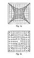
- the pin cushion effect of Figure 1ais well understood. It arises from the current sharing of capacitance-induced flows from the point of touch to the four connection points; the effect is seen in both 2DCT's and in 2DRT 5-wire touch screens which rely on a galvanic version of the same voltage gradients as a 2DCT, but with a flexible 'pickoff' cover sheet that deflects and connects to the 2DRT under pressure.
- the pin cushion effect in these elementsincreases as the location of touch becomes more distant from all connection points, along an edge; it is at its worst at the centers of the screen edges.
- the current flowsestablish vectors that introduce a graduated distortion with position, resulting in a parabolic curvature of reported location.
- the vectorsare generally non-orthogonal. Instead the angle and magnitude of correction vary wildly depending on the location of touch on the element.
- Embodiments of the inventionprovide a compromise between the 'no pin cushion' but expensive circuitry and fabrication cost of prior-art striped elements, and unpatterned resistive sheet elements.
- This new hybrid solutionproduces a pin cushion effect only on one axis, leaving the other axis largely undistorted.
- the residual pin-cushion distortionhas a largely orthogonal and predictable vector which can be compensated using relatively trivial numerical methods, is highly repeatable from unit to unit, and is more immune to differential thermal drift than the prior art.
- FIG. 3is shown a pattern representative of the conductive material used in a sensing element according to an embodiment of the invention.
- the diagramshows a single conductive element on one layer having four electrodes 301, 302, 303, and 304.
- Two relatively low resistance bus-bars 305 and 306traverse from 301 to 302, and 304 to 303 respectively.
- a plurality of stripe conductors 310traverse from bus-bar 305 to 306, numbering at least two but typically 3 or more. Two of these stripes traverse from the ends of each bus-bar to the other, thus forming a fully bounded surface.
- the end stripescan also be considered to be bus-bars, but as they can optionally have a higher path resistance than the horizontal bus-bars shown, they remain unique and thus will be called stripes throughout.
- the element of the inventioncan alternatively be viewed as having a core area characterized by anisotropic conductivity with a surrounding, bounding border made from linear conductive segments.
- the purpose of the stripesis to force anisotropic galvanic flows within the core area. Once the current flows reach the boundary paths, they are finally led to the electrode connections.
- Wires 312a-d connected to the electrodesconnect the element to a drive / sensing circuit in the case of a 2DCT.
- wires 312a-dare connected to a drive circuit, the sensing function coming from a flexible user-depressed cover sheet as shown in Figure 11 .
- Figure 10shows another pattern embodying the invention.
- This patternis substantially the same as the pattern of Figure 3 except that the stripes are separated by thin slits (i.e. the stripes are relatively wider than those shown in Figure 3 ), so that the element is principally coated with conductive material and only a very small percentage - the slits - is uncoated.
- This configurationis more suitable for 2DRT use as described further below, but can also be used in 2DCT applications.
- One advantage of this for 2DCT useis that the stripes have larger surface areas than in the Figure 3 example, so that the capacitive coupling from finger to element is enhanced.
- One disadvantage of thisis that the total resistance from bus-bar to bus-bar is lower for a particular sheet resistance, which will tend to exacerbate the pin cushion effect as described below.
- the relative resistances of the stripes and bus-bars in Figure 3 as testedare about 40K ohms for the bus-bars, and 160K ohms for the stripes, although in practice these figures are only for guidance and they are not limiting to the invention.
- the use of higher resistance value stripes than bus-barsis helpful to limit pin cushion effects, but since pin cushion is easily correctable numerically anyway, almost any combination of values will work to varying degrees of satisfaction. It is a considerable attraction of the invention that it is usable with elements having a high resistance, as such an element requires lower cost and lower power drive and sensing electronics.
- Figure 4shows a lumped model of typical embodiments of the invention.
- Bus-bars 305 and 306are composed of lines with a resistance from about 1K to 50K ohms, and ideally are matched to within 10% of each other.
- Stripes 310are composed of resistive lines of about 5 to 10 times more than the resistance of the bus-bars. There are 9 stripes shown in Figure 4 .
- Corner electrodes 301, 302, 303, and 304are used to connect the element to drive / sensing electronics, either capacitive sensing drivers for a 2DCT or galvanic drivers in the case of a 2DRT.
- Each stripe and bus-barhas some stray background capacitance 401 to circuit ground. Stripes have mutual capacitance 404 between neighbors.
- the inventionis fully tolerant of the magnitude of Ct, in that it allows the use of circuitry and / or algorithms that responds ratiometrically to the four electrode signals to derive a position independent of the magnitude of Ct.
- the coversheetpicks off a gradient potential, usually using time-multiplexed drive signals to the four electrodes upon galvanic connection from the coversheet to the element under the pressure of touch.
- Figure 5shows the element with a touch capacitance geographically located at 403 due to finger (not shown).
- Figure 6in which is shown a cross section of the invention attached to a substrate such as glass.
- the capacitance 603 due to touch of finger 605is split into three smaller parts, Ct1, Ct2, and Ct3 as shown in Figure 6 , whose ratio depends on the relative location of the touch among the stripes 310a,b,c..
- Figure 6 of my co-pending US application 60/422837 [28]is shown an interpolation between two adjacent electrodes connected by a resistance.
- the interpolation of touch in the instant inventionoperates in exactly the same manner among stripes in X, but also occurs along each stripe in the Y axis (not shown).
- the separating resistance in Xis the path starting on each stripe with each Ct 603, back through the bus-bars to the other stripe.
- the interpolation in the X directionis proportioned according to the resistance of the short segment of bus-bar resistance connecting the two Y stripes, as a percentage of the total electrical bus-bar 'length'.
- the resistance of the stripe itselfis not of consequence for resolving X location, since the ends of each stripe are driven to equipotentials in most 2DCT drive circuits described in the literature, and certainly when driven by the charge-transfer circuits described in my various earlier patent publications.
- the stripesare spaced apart by 10% of the total bus-bar length, then the opportunity for interpolation will be 10% of the X dimension.
- the measurement circuitryis used by standard connection to the four corner electrodes 301, 302, 303, and 304.
- the measurement circuitrycomprises four drive channels coupled to respective ones of the electrodes shown in Figure 3 with each channel being operable to generate an output signal dependent on the resistive path length between its electrode and the position of the touch. While other methods might use other formulae, the p referred method of calculation of the position of touch is an adaptation of the one disclosed in my co-pending application 60/422837 [28].
- the four corner signalsare calibrated at some time to determine a baseline reference level of signal for each corner.
- the calibration stepcan occur once, for example during design, on the production line, or at each power-up event, or through a method that determines when the element is not being touched.
- Drift compensationcan be applied as it is known from several of my prior patents and the datasheets of products from Quantum Research Group Ltd (UK), such as the QT110 device [38].
- the signalsare processed according to the following steps assuming that the real time acquired signals associated with the four electrodes 301, 302, 303 and 304 are respectively S301, S302, S303, and S304, and the baseline reference levels are R301, R302, R303, and R304, respective to each corner:
- Figure 6is shown a touch 601 over a plurality of stripes creating a distribution of Ct over said stripes.
- the resultant chargeflows in the element set up an areal distribution of Ct couplings across multiple stripes, roughly in proportion to the adjoining surface areas of touch and stripes.
- the principle of superpositionapplies (as it does in any sheet element) and the resultant determination of position will be properly weighted and hence located to a far higher effective resolution than the number of stripes would seem to indicate.
- Figure 7bschematically represents the distortion over all quadrants of the sensing element A finger touching the element, whose circumference of contact encompasses a fractional number of stripes, shows no cogging or nonlinearity in X worth noting when dragged orthogonally to the stripes. This can be seen more graphically in Figure 8 which shows a plot of the correction vectors for 7 rows cutting across the stripes in X. At no place is there a non-orthogonal, non-vertical correction vector.
- Figs 7a, 7b , and 8show that in the Y axis the distortions are linear and can be corrected using a simple scaling factor which has a dependency on X.
- a simple scaling factorwhich has a dependency on X.
- For each position in X, there exists a single scalar (non-vector) correction factor which can be use to arrive at a corrected position of touch in Y: Pcy x yP Y ⁇ X
- the elementis also more stable under fluctuating temperature or electrical conditions and is more repeatable to manufacture.
- the correction of the elementdoes not require multiple trials to allow curve fitting. So long as the strip-to-bus-bar resistance ratio is repeatable (absolute stability is not required), the factors ⁇ (x) will be the same from one unit to the next. Inconsistencies from unit to unit will have only a limited effect on the error term in reported touch location, and errors on one axis will create only highly attenuated errors on the other axis.
- the element of the inventiongenerally isolates error terms between X and Y, a non-trivial beneficial effect compared with the prior art.
- the simplicity of the instant inventionshould be compare with the '80 coefficients' and fourth order polynomials required for Babb, the coefficients of which must be determined though an extensive calibration procedure.
- the instant inventionmay require only single point calibration, or in most cases no calibration at all, as element distortions are simple, predictable, and repeatable from unit to unit.
- the ⁇ (x) correction factorscan be applied by means of a lookup table with interpolation to achieve a simple, fast correction.
- k1, k2 and k3are coefficients that depend on the curvature of pin-cushion distortion
- Xis the absolute magnitude of the position along the X axis starting from center-screen and moving in either the left or right direction.
- This quadratic equationwas derived from simulation models and is accurate to better than 1%. It does not account for gross material nonlinearity which can be compensated for using secondary methods if required.
- the equationsare dependent on resistance ratios between the bus-bars and the stripes as well as the geometric proportions of the element. The equations are unaffected by absolute resistance values.
- a 2DRTgenerally operates in 'reverse' to a 2DCT in that the element is only driven by signals, which are then picked off by a coversheet using a 5 th electrode connection for analysis purposes.
- the electrodes on the element properare usually driven in a time-multiplexed mode so as to allow for unique signals to be picked up in alternating X and Y directions. For example the two left electrodes are first grounded, and the two right ones driven to a fixed and identical potential; the cover sheet is sampled to obtain a raw X position. The bottom electrodes are next grounded, and the top electrodes connected to a fixed and identical potential; the cover sheet is sampled to obtain a raw Y position.
- Equation 5needs only a set of solutions in one quadrant, with the results mirrored for the other 3 quadrants. This is demonstrated in figure 7a and 7b.
- Figure 7ashows the distortion i n the t op right quadrant; this pattern is mirrored in the other three quadrants to create the pattern of 7b.
- a second methodinvolves essentially repeating the element of the invention a second time as shown in Figure 9 .
- thiscan be achieved by effectively sharing a bus-bar to reduce associated component counts.
- the patternis excited by driver/sensor circuitry on the 6 nodes (i.e. electrodes) 301, 302, 301a, 302a, 303 and 304 as shown, the element is effectively divided up in a way that allows it to be sensed in two different zones, top and bottom. Sensing within these zones is as described above.
- handshadow capacitanceoccurs primarily below the point of touch, a touch in the upper zone will cause handshadow primarily in the lower zone, where it can be 'processed away' by simply ignoring the signals from said lower zone. There is very little cross-coupling of handshadow currents between zones.
- Figure 10shows an element having slits between stripes. Such a method of separating stripes is particularly useful for 2DRT usage, where a cover sheet is deflected to contact the element at a small point. If the point of contact is smaller than the gap between stripes 310, it can be that the coversheet fails to pick up a potential and the contact fails.
- Figure 11shows a resistive screen according to the invention, wherein a cover sheet picks off a galvanic potential from the slit stripes of Figure 10 when bent inwards via touch or via a stylus.
- the element of figure 11is exactly as described above for a 2DCT, but the operating mode is according to various 5-wire screen modes a s discussed i n other patents and in the open literature. Normally the cover sheet is held apart from the element via tiny 'microbump' spacers (not shown), as is well known in the art.
- Figure 12shows a minimal 2DCT case, where there are 2 bus-bars and two stripes, all on the periphery of an element.
- the elementis of a size not significantly larger than the object being sensed, so that the signal levels in the middle do not significantly diminish due to distance from object to each conductive member.
- This exampleoperates without measurable pin cushion as the impedances of the stripes and bus-bars are many orders of magnitude lower than the capacitive coupling impedance from object to any strip or bus-bar.
- the stripes and bus-barscan have the same value or wildly differing values with minimal observable effect on resolution or linearity.
- the element of Figure 12is for use by a human finger, the element should preferably be no more than 4 times as wide or high as the diameter of a finger in order to provide reasonable signal strengths.
- the element of Figure 12can be used to create a 'mini mouse pad' or pointer control, for example for use by those with minimal appendage mobility, whereby very small motions of a fingertip or other appendage control an appliance or GUI.
- the 2DCT elementis suited to use in a 'point mode' where the user simply points at the screen.
- the easily correctable pin cushion and use of a single elementmean that fields are not localized to short distances.
- the inventioncan be used as a 'point screen' device with reasonable accuracy in most menu-based graphical interfaces.
- This mode of operation can be extremely beneficial in hygiene applications such as in hospitals, b ut also in ordinary consumer usage modes to prevent screen smudging.
- FIG. 13wherein is shown preferred (but not essential) drive circuitry for the 2DCT application of the invention.
- This circuitis of the same type as shown in my co-pending US application 60/422837 [28] but applied to all 4 electrodes (or 6 electrodes in the case of Figure 9 , etc).
- the repeated switching of switches 1302, 1303, 1304 at locations A, A', A", A"', B, B', B", B"', and C, C', C", C"'are performed simultaneously at each electrode so as to inject and measure charge using four capacitors, also referred to as sampling capacitors, Cs, 1305, at equal moments in time. This is performed via switch controller 1307.
- Signal outputsare the tabulated number of switching cycles for each electrode required to exceed a threshold voltage Vt, as determined by a voltage comparator 1301.
- the tabulation of cycle counts for each electrodeis performed by four counters at 1306.
- the inventioncan alternatively employ any of the switching sequences and topologies as described in my US Patent 6,466,036 [34].
- Signal processing circuitryis shown in Figure 14 , wherein the four electrode signals are input to the processing circuitry which in turn computes a coordinate result.
- a logic block, microcontroller, or other hardware or softwareis used to perform the calculations necessary to achieve the desired output.
- the block of Figure 14is usually a part of another system, such as a personal computer, process controller, appliance and so on, and the output may b e only a n intermediate result i n a larger process.
- Figure 15shows a preferred embodiment of the invention wherein a single microcontroller 1501 performs the switching functions of Figure 13 , plus performs the signal processing of Figure 14 .
- the switching functionscan be performed in software on a conventional I/O port, or with an on-chip hardware capacitive conversion peripheral.
- Signal processingis performed in software to achieve the desired coordinate output. This output could be a mere intermediate result used to control a larger process, and the output shown may only exist as numbers inside the chip.
- the inventioncan use any capacitive or resistive sensing circuit described in literature.
- the gradient response of the elementis normally the same regardless of the type of drive circuitry.
- the inventionis not reliant on any one acquisition method.
- the 2DxT elementis preferably made of a clear conductor of suitable resistance on the back of a glass or plastic sheet covering the display, if a touchscreen, or over a suitable dielectric substrate if a mousepad, etc.
- the need for low-R bus-bars (under about 200 ohms end-to-end) on the edgescauses all manner of driving, power, stability, and repeatability issues. It is highly desirable to use materials with a much higher resistance than currently in widespread use. Most ITO (Indium Tin Oxide) layers such as those produced by CPFilms, USA, or when c ustom-sputtered onto a surface, have resistances around 300 ohms per square. It is highly desirable to elevate this resistance to the neighborhood of 500 to 2000 ohms per square, so that the stripe and bus-bar resistances can be made in the region of 25K ohms and up from end to end.
- ITOIndium Tin Oxide
- One method of increasing bus-bar and stripe resistance from low resistance materialsis to use a meandering path or zig-zag pattern so as to increase track length.
- Conventional low-resistance ITO or Tin-Oxide coatingscan be etched or patterned to have intentional voids ('Swiss cheese' approach), thus raising the resistance.
- the stripes and bus-barscan also be made suitably thin so that the resistance is high enough to be more optimal.
- Agfa's OrgaconTM conductive polymeris one material that has such a high intrinsic resistance and is also clear, making it usable in touch-screens over displays.
- a particularly low cost materialis carbon based ink, well known in the electronics trade, however being opaque this material is better suited for tablet or mousepad applications.
- the driving circuitrycan be adapted to almost anything with varying degrees of difficulty.
- the elementshave a non-zero resistance.
- the bus-bar resistancesshould preferably be comparable or lower in value than the aggregate parallel value of the stripes in order to reduce Y-axis pin cushion. A greater number of stripes would generally m ean a higher resistance per stripe to achieve the same effect, the pin cushion being related to the total bridging resistance between stripes, the bridging resistance being the parallel equivalent value of the stripes. Stripes located towards the center of the bus-bars have a disproportionate effect on pin cushion.
- Patterning of the element into bus-bars and stripescan be via vapor deposition using a suitable stencil to prevent unwanted areas of coating, or via silk screening to create the desired pattern, or via pad-printing, or via laser scribe or chemical etching or chemical reaction, or any other process which can create a patterned layer.
- the patterncan be created by using sodium hypochlorite to force areas to become non-conductive via chemical reaction without actual material removal.
- Fabricationcan entail the use of normal touchscreen or touchpad methods such as vapor deposition of appropriate materials onto a glass sheet placed in front of a display.
- IMDIn-mold decorating
- 2DCTIn-mold decorating
- a conductive element of the type according to the inventionis placed in the mold for a display cover; when injected, the conductive layer becomes fused to one side of the cover.
- Electrode connectionscan be made via wires bonded to the corners, or via conductive rubber pillars, or using metal springs, etc.
- Conductive rubberis a method of choice for very low cost connection from an underlying PCB containing the driver circuitry.
- Figure 16shows such a construction method in cross-section.
- Display 1601is viewed through cover lens 1602 and sensing element 300.
- Element 300is connected via at least four corner electrodes through conductive rubber posts, of which two 1603a, 1603b are shown, to PCB 1604.
- the entire assemblyis placed under compression via screws, clamps or other fastener system (not shown) so that the rubber posts are compressed and thus forced to make contact between PCB 1604 and element 300.
- the elementcan also be fabricated from molecular substances having anisotropic conduction.
- a conductive polymercan be envisioned having conductivity that is much better in one direction than another.
- Such materials based on nanostructureshave been described in the literature, for example in literature from Helsinki University of Technology.
- One embodiment of the inventionweights the stripes so that the ones near center-screen are either spaced further apart or have a higher resistance or both. The effect of this is to reduce the amount of inherent pin cushion. However, tests have shown that while this in fact is what happens, it also means that there will be a loss of signal in the center of the element, and/or there will be drive problems through the resultant higher resistance and lower finger coupling to neighboring traces. In practice this approach is not deemed to be efficacious, and is mentioned here only for completeness.
- problems associated with 2DCT'sinclude interference from outside electrostatic or radio sources having a frequency at the operating frequency of the element, or some harmonic thereof. These problems can be attenuated by using a modulated operating frequency for the signal acquisition so as to reduce or prevent signal-noise aliasing or beating. This can involve the use of frequency hopping, chirps, or pseudo-random frequency modulation. These methods are known as 'spread-spectrum' modulation.
- Post processingcan include the use of majority vote filtering, median filtering, averaging, and so on to reduce the residual effects of noise that are already attenuated by means of the frequency modulation.
- Low frequency interferencecan be caused by local mains fields and so on.
- This form of interferencecan be attenuated by synchronizing the acquisition to the interfering source, for example 50 or 60 Hz, as described in the datasheet for the Quantum Research Group Ltd (UK) QT310 device [40].
- the elementis compatible with driven shield methods to reduce interference from LCD displays, VFD switching, etc. This entails the use of a conductive plane behind the element positioned between the element and the interfering source.
- a drive shieldcan also protect against signal disturbance from motion behind the element. Driven back-shields are commonly used in the construction of 2DCT's.
- the elementcan be driven as a single large capacitive electrode without regard to position location, while the unit is in the background state.
- the electronic driver logiclooks for a very small change in signal, not necessarily enough to process as a 2D coordinate, but enough to determine that an object or human is in proximity.
- the electronicsthen 'wakes up' the overall system and the element is driven so as to become a true 2DCT once again.
- the element of the invention in 2DCT modeis suitable as a mouse pad, or as a tablet type input device. In these roles, there is no need for optical transparency.
- a styluscan be used with the element either to pick up a radiated electric field from the element, or to inject a signal into the element, or to act as a human finger.
- the element of the inventionmerely operates in reverse.
- a signal from a tethered penis injected capacitively into the element in a region surrounding the point of contact.
- the signalis then apportioned ratiometrically to the four corner electrodes, from whence it can be picked up and conveyed to a measurement circuit of almost any type already described in literature and then processed to create an indicative result.
- the pin cushion resultoperates in substantially the same way in injection mode as it does in a 2DRT or 2DCT mode; the vector gradients are the same.
- the accuracy of the raw processed resultmay be acceptable for direct use.
- the elementmay be perfectly suitable for uncorrected menu button detection over a display where the buttons do not occupy less than 10% of the height of the element. If the buttons are principally located near the horizontal centerline of the element, or along the left or right sides, the distortion could be negligible and if so, no linearization correction need be applied.
- the inventionis at its basic reduction, an element whose purpose is to provide for an improved form of 2D sensing device via anisotropic conduction, plus, optionally, a method to correct the distortions of the raw computed coordinate result.
- the mode of operationincluding but without limitation, galvanic or capacitive modes), the use to which it is put, and whether it is used as a receiver of signals from a stylus or a sensor of passive touch is not of prime importance to the invention. What is important is the anisotropic structure of the element and the form of positional error it produces, and the optional methods disclosed herein for correcting the error.
- sensing elements of embodiments of the inventioncan be made as a single-layer having a core that conducts well galvanically in a first predetermined direction, but suppresses conduction in a second direction orthogonal to the first, i.e. it has anisotropic conductivity, plus, the core is bounded by a resistive border to make the whole element.
- the elementfurthermore has four electrodes in the corners and which are driven and/or sensed by an electronic circuit to create a resulting output indicative of touch position.
Landscapes
- Engineering & Computer Science (AREA)
- General Engineering & Computer Science (AREA)
- Theoretical Computer Science (AREA)
- Human Computer Interaction (AREA)
- Physics & Mathematics (AREA)
- General Physics & Mathematics (AREA)
- Position Input By Displaying (AREA)
Description
- The invention pertains to 2-dimensional touch sensing surfaces operable by a human finger, or a stylus. Example devices include touch screens and touch pads, particularly those over LCDs, CRTs and other types of displays, or pen-input tablets, or encoders used in machinery for feedback control purposes.
- Descriptions of pen or touch input to a machine date back to at least 1908, as embodied in patent
DE 203,719 [1]. - Touch screens and pointing devices have become increasingly popular and common not only in conjunction with personal computers but also in all manner of other appliances such as personal digital assistants (PDAs), point of sale (POS) terminals, electronic information and ticketing kiosks, kitchen appliances and the like. These devices are evolving continuously into lower priced products and as a result, there is a need for ever lower production cost while maintaining high levels of quality and robustness. Capacitive touch screens in particular are prized for their robustness against damage, but suffer from high costs and the need for exotic construction materials.
- The term 'two-dimensional capacitive transducer' or '2DCT' will be used throughout to refer to touch screens, touch sensing pads, proximity sensing areas, display overlay touch screens over LCD, plasma, or CRT screens or the like, position sensing for mechanical devices or feedback systems, or other types of control surfaces without limitation, having a surface or volume capable of reporting at least a 2-dimensional coordinate, Cartesian or otherwise, related to the location of an object or human body part, by means of a capacitance sensing mechanism.
- The term 'two-dimensional resistive transducer' or '2DRT' will be used throughout to refer to touch screens or pen input devices based on purely galvanic principles, and known in the industry generically and primarily as 'resistive touch screens'.
- The term '2DxT' refers to elements of either the 2DCT or 2DRT type.
- The term 'touch' throughout means touch or proximity by a human body part or mechanical component of sufficient capacitive signal strength to generate a desired output. In the sense of 'proximity', touch can also mean to 'point' at a 2DCT without making physical contact, where the 2DCT responds to the capacitance from the proximity of the object sufficient to react properly.
- The term 'element' throughout refers to the active sensing element of a 2DCT or 2DRT. The term 'electrode' refers to a connection p oint at the periphery of the element.
- The term 'stripe' refers to an electrical line conductor that is a component part of an element and which has two ends. A stripe can be a wire. A stripe can have substantial galvanic resistance by intent, whereas a wire has minimal resistance. If the element of which it is a part is physically curved, the stripe would also be physically curved.
- The term 'pin cushion' refers to any distortion of the signal from a 2DCT whether parabolic, barrel, or other form of 2D dimensional aberration.
- Many types of 2DCT are known to suffer from geometric distortion characterized as 'pin cushion' or 'hyperbolic' or 'parabolic', whereby the reported coordinate of touch is in error due to electrical effects on the sensing surface. These effects are described in more depth in various other patents for example in
Pepper US 4,198,539 [2]. An excellent summary of the known causes, solutions, and problems of the solutions to geometric distortion can be found in a reading ofB abb et al, in US 5,940,065 [3] a ndUS 6,506,983 [4]. US 5,940,065 [3] describes succinctly the two major classes of correction: 1) Electromechanical methods involving design of or modification to the sensing surface or the connecting electrodes; 2) Modeling methods using mathematical algorithms to correct the distortions.- Edge Manipulation of Planar Element:
Küpfmüller et al in US 2,338,949 [5] (filed 1940) solve the problem of edge distortion in a 2DRT electrograph using very long rectangular tails in X and Y surrounding a small usable area. Küpfmüller takes the further approach of slotting the four tails into stripes; these stripes do not intrude on the user input area but do act to raise the resistance to current flow in an anisotropic manner along sides parallel to current flow. This idea reappears in slightly different form inYaniv et al, US 4,827,084 [6], nearly 50 years later. Küpfmüller remains the most similar prior art to the instant invention. Becker in US 2,925,467 [7] appears the first to describe a 2DRT electrograph whereby nonlinear edge effects are eliminated via the use of a very low resistance edge material relative to the sheet resistance of the element proper. This method can also be used to construct a 2DCT.Pepper, in patents US 4,198,539 [2],US 4,293,734 [8], andUS 4,371,746 [9] describes methods of linearizing a 2DCT by manipulating the edge resistance structure of the element.Talmage, in US 4,822,957 [10] describes a similar edge pattern as Pepper in conjunction with a 2DRT element and a pickoff sheet. Numerous other such patents have been issued using various methods, and the area remains a fertile one for new patents to this day. These methods have been found to be very difficult to develop and replicate, and they are prone to differential thermal heating induced errors and production problems. Very small amounts of localized error or drift can cause substantial changes in coordinate response. The low resistance of the patterned edge strips causes problems with the driver circuitry, forcing the driver circuitry to consume more power and be much more expensive than otherwise. There are a significant number of patents that reference the Pepper patents and which purport to do similar things. The improvements delivered by Pepper etc over Becker are arguably marginal, as at least Becker is easier and more repeatable to fabricate.- Edge Resistance with Wire Element:
Kable in US 4,678,869 [11] discloses a 2D array for pen input, using resistive divider chains on 2 axes with highly conductive electrodes connected to the chains, the electrodes having some unintended resistance for the purposes of detection, and the detection signal being interpolated from the signals generated between two adjacent electrodes. The unintended resistance causes a slight amount of pin cushion in the response. This patent also describes an algorithmic means to compensate for the slight pin-cushion distortion developed by this technique. The Kable method is not operable with other than a connected s tylus, i.e. it is not described as being responsive to a human finger. The Kable patent requires crossovers between conductors and thus needs at least three construction layers (conductor, insulator, conductor). - Multiple Active-Edge Electrodes:
Turner in US 3,699,439 [12] discloses a uniform resistive screen with an active probe having multiple electrode connections on all four sides to linearize the result. Yoshikawa et al, in US 4,680,430 [13], andWolfe, in US 5,438,168 [14], teach 2DCT's using multiple electrode points on each side (as opposed to the corners) to facilitate a reduction in pin cushion by reducing the interaction of the current flow from the electrodes on one axis with the electrodes of the other. While the element is a simple sheet resistor, this approach involves large numbers of active electronic connections (such as linear arrays of diodes or MOSFETs) at each connection point in very close proximity to the element.Nakamura in U S 4,649,232 [15] teaches similarly as Y oshikawa and Wolfe but with a resistive pickup stylus.- Sequentially Scanned Stripe Element:
Greanias et al in US 4,686,332 [16] andUS 5,149,919 [17],Boie et al in US 5,463,388 [18], andLandmeier in US 5,381,160 [19] teach methods of element sensing using alternating independently driven and sensed stripe conductors in both the X and Y axis, from which is interpreted a position of a finger touch or, by a pickup device, a stylus pen. The construction involves multiple layers of material and special processing. Greanias teaches the use of interpolation between the stripes to achieve higher resolution in both axis. Both require three or more layers to allow crossovers of conductors within the element. Both rely on measurements of capacitance on each stripe, not the amount of cross coupling from one stripe to another. Boie also teaches a special guard-plane. Binstead, in US 5,844,506 [20] andUS 6,137,427 [21] teaches a touch screen using discrete fine wires in a manner similar to those taught by Kable, Allen, Gerpheide and Greanias. Binstead uses very fine r ow a nd column w ires t o a chieve transparency. This patent also teaches the Greanias method of interpolation between electrode wires to achieve higher resolution. The scanning relies on measurements of capacitance on each stripe to ground, not the amount of cross coupling from one to another.Evans in US 4,733,222 [22] also describes a system wherein stripes are sequentially driven in both X and Y axis, using also an external array of capacitors to derive sensing signals via a capacitor divider effect. Interpolation is used to evaluate finer resolutions than possible with the stripes alone.Volpe in US 3,921,166 [23] describes a discrete key mechanical keyboard that uses a capacitive scanning method. There are sequentially driven input rows and sequentially sensed columns. The press of a key increases the coupling from a row to a column, and in this way n-key rollover can be achieved; there is no need for interpolation. Although not a 2 DCT, Volpe presages scanned stripe element 2DCT technology. My ownUS 6,452,514 [24] also falls into this classification of sensor.Itaya in US 5,181,030 [25] discloses a 2DRT having resistive stripes which couple under pressure to a resistive plane which reads out the location of contact. The stripes, or the plane, have a 1D voltage gradient imposed on them so that the location of contact on particular the stripe can be readily identified. Each stripe requires its own, at least one electrode connection.- Cyclical Scanned Stripe Element:
Gerpheide et al, in US 5,305,017 [26] teaches a touch-pad capacitance-based computer pointing device using multiple orthogonal arrays of overlapping metallic stripes separated by insulators. The scan lines are arranged in a cyclically repeating pattern to minimize drive circuitry requirements. A cyclical nature of the wiring of the invention prevents use of this type of 2DCT for absolute position location. The invention is suited to touch pads used to replace mice, where actual location determination is not required, and only relative motion sensing is important. Gerpheide teaches a method of signal balance between two phase-opposed signals at the location of touch. - Parallel Read Stripe Element:
Allen et al in US 5,914,465 [27] teach an element having rows a nd columns can s tripes which a re r ead i n parallel by analog circuitry. The patent claims lower noise and faster response times than sequentially scanned elements. The method is particularly suited to touch pads for mouse replacement but does not scale well to higher sizes. Multiple construction layers are required as with all stripe element 2DCT's. The Allen method requires large scale integration and high numbers of connection pins. It interpolates to achieve higher resolution than achievable by the number of raw stripes. - In my co-pending
US application 60/422837 Figure 12 a method of using individual resistive 1-D stripes to create a touch screen. These stripes can be read either in parallel or sequentially, since the connections to these stripes are independent of one another. Furthermore, in connection withFigure 6 there is described an interpolated coupling between adjacent lumped electrode elements and an object such as a finger.US-A-5818430 is acknowledged in the preamble ofclaim 1. Nakamura in US 4,650,926 [29] describes a system for numerical correction of an electrographic system such as a tablet, using a lookup table system to correct raw 2D coordinate data.Drum, in US 5,101,081 [30] describes a system for numerical correction of an electrographic system such as a tablet via remote means.McDermott in US 5,157,227 [31] teaches a numerical method of correcting a 2DxT employing stored constants which are used during operation to control one or more polynomials to correct the location of reported touch by zone or quadrantBabb et al, in US 5,940,065 [3] and6,506,983 [4] teach a numerical method to linearize a 2DxT uniform sheet element using coefficients determined during a learn process, without segmentation by zone or quadrant, and on an individual unit basis so as to correct for even minor process variations. The methods disclosed by Babb are complex and involve '80 coefficients' and fourth order polynomials, the coefficients of which must be determined through a rigorous and time-consuming calibration procedure. In tests supervised by the instant inventor, it has been found that 6th order polynomials are required to produce accuracy levels that are acceptable in normal use, and that the result is still highly prone to the slightest subsequent variations post-calibration due to thermal drift and the like. In particular it has been found that the corner connections are extreme contributors to long-term coordinate fluctuations, as they act as singularities with a high gain factor with respect to connection size and quality. Furthermore, the method of numerical correction requires high-resolution digital conversions in order to produce even modest resolution outputs. For example it has been found that a 14-bit ADC is required to provide a quality 9-bit coordinate result. The extra expense and power required of the amplifier system and ADC can be prohibitive in many applications.- In all these methods there exists one or a combination of the following deficiencies:
- Use of exotic construction materials or methods requiring special expertise or equipment to fabricate;
- Excessive cost compared with simple, galvanic 4-wire resistive touch screens;
- Require three or more layers to allow orthogonal conductor crossovers;
- Costly wiring due to the need for many electrode connections;
- Linearity problems requiring complex algorithms to correct;
- Need for special linearizing edge patterns which are difficult to control;
- Not well suited to small or large touch areas;
- Inability to conform to complex surface shapes such as compound curves; and/or
- Inability to operate through surfaces more than a few hundred microns thick.
- According to the invention there is provided a touch sensitive position sensor comprising: a substrate defining a touch sensitive platform; first and second resistive bus-bars arranged spaced apart on the substrate; and an anisotropic conductive area having non-zero resistance arranged between the bus-bars such that currents induced in the anisotropic conductive area flow preferentially towards the bus-bars, wherein the bus bars and anisotropic conductive area reside on a single layer, and their resistances are such that the position of an object can be estimated in two dimensions without requiring a further layer of conductive material.
- In typical embodiments of the invention, the bus-bars and the anisotropic conductive area have resistances of between 1 kΩ and 50 kΩ. The bus-bars preferably have substantially the same resistance, for example to within +/-10%, 20%, 50% or 100%. It is advantageous if the resistance of the bus-bars is less than the resistance between them provided by the anisotropic conductive area.
- The anisotropic conductive area can be fabricated using a film of molecular substance having anisotropic conduction supported on a substrate, or a plurality of resistive stripes connecting in parallel between the first and second resistive bus-bars, or in other ways.
- When resistive stripes are used to form the anisotropic conductive area these can be made of sections of resistive wire, or from resistive material deposited on a substrate, for example. Moreover, the width of the resistive stripes is preferably greater than the gaps between them.
- In some embodiments of the invention, a conductive overlay is provided that is separated from the anisotropic conductive area such that the conductive overlay and the anisotropic conductive area may be brought into contact by externally applied pressure.
- In some embodiments, the first resistive bus-bar extends between a first and a second electrode and the second resistive bus-bar extends between a third and a fourth electrode, the position sensor further comprising first, second, third and fourth drive channels associated with respective ones of the first, second, third and fourth electrodes, each drive channel being operable to generate an output signal dependent on the resistance between its electrode and the position of the object. For processing the outputs, a processor may be provided that is operable to generate an estimate for the position of the object by comparing the output signals from the drive channels. The processor can be configured to estimate the position of the object in a first direction running between the bus-bars from a ratiometric analysis of the sum of the signals associated with the first and second electrodes and the sum of the signals associated with the third and fourth. It can also be configured to estimate the position of the object in a second direction running along the bus-bars from a ratiometric analysis of the sum of the signals associated with the first and third electrodes and the sum of the signals associated with the second and fourth electrodes. Moreover, the processor is preferably further operable to apply a correction to the estimated position according to a pre-determined distortion associated with the sensing element. Typically, the pre-determined distortion is a one-dimensional pin-cushion distortion.
- It will be understood that a touch sensitive position sensor according t o the invention can be incorporated into a control panel and in turn the control panels can be integrated as part of a variety of different apparatuses.
- According to the invention there is also provided a t ouch sensitive position sensor for detecting the position of an object in two dimensions, wherein the position sensor has first and second resistive bus-bars separated by an anisotropic conductive area, the anisotropic conductive area being arranged such that induced electric currents flow preferentially towards the bus-bars. Because induced currents, for example those induced by drive circuitry associated with the sensing element, flow preferentially along one direction, pin-cushion type distortions in position estimates are largely constrained to this direction. Such one-dimensional distortions can be corrected for by applying scalar correction factors.
- The invention provides a new pattern of conductive material for sensing capacitance behind a plastic or glass panel or other dielectric, which is to be used as a 2DxT, whether in the format of a touch screen or 'touch pad'.
- The invention blends some of the features of unpatterned 4-electrode elements together with striped elements and mathematical compensation to arrive at a new classification of anisotropic 2DxT element, or simply, a 'striped element'. This invention addresses the deficiencies of previous 2DxT approaches and is very low in cost, using as it does conventional processes and materials.
- Unless otherwise noted hereinafter, the terms 'connection(s)' or 'connected' refer to either galvanic contact or capacitive coupling. 'Element' refers to the physical electrical sensing element made of conductive substances. 'Electrode' refers to one of the galvanic connection points made to the element to connect it to suitable driver/sensor electronics. The terms 'object' and 'finger' are used synonymously in reference to either an inanimate object such as a wiper or pointer or stylus, or alternatively a human finger or other appendage, any of whose presence adjacent the element will create a localized capacitive coupling from a region of the element back to a circuit reference via any circuitous path, whether galvanically or non-galvanically. The term 'touch' includes either physical contact between an object and the element, or, proximity in free space between object and element, or physical contact between object and a dielectric (such as glass) existing between object and element, or, proximity in free space including an intervening layer of dielectric existing between object and element. The mention of specific circuit parameters, or orientation is not to be taken as limiting to the invention, as a wide range of parameters is possible using no or slight changes to the circuitry or algorithms; specific parameters and orientation are mentioned only for explanatory purposes.
- Note my prior patents covering charge-transfer capacitive sensing, particularly
US 5,730,165 [32],US 6,288,707 [33],US 6,466,036 [34],US 6,535,200 [35],US 6,452,514 [36] and my co-pendingUS provisional application 60/422837 - Note also my co-pending US application
US 20030132922 [37] which deals with handshadow effects on capacitive touchscreens, and which has a possible application to the invention in a post-processing role for 2DCT's. - My co-pending US patent application
US 60/422837 Figure 12 therein, forms a germinal basis for the invention, and whose circuit description and switching methods are particularly well adapted to drive the electrodes of the invention in a 2DCT mode. The invention is a new pattern of conductive material, such as an ink or vacuum deposited material, arranged electrically as a single layer element, with pin-cushion distortion on only one axis. The remaining pin-cushion distortion is easily corrected algorithmically or in hardware, vastly simpler than Babb & Wilson, as will be described below. The element pattern is easily fabricated using known methods and is conformable to complex surfaces such as compound curved cover lenses and the like. The pattern exhibits strong anisotropic conductance characteristics in a core sensing region bounded by peripheral unidirectional resistive conductors. - It is one object of the invention to provide for a 2DxT sensing element using common, inexpensive materials and production processes, with anisotropic galvanic conduction characteristics.
- It is a further object of the invention to provide a 2DxT sensing mechanism having an edge distortion that is readily correctable using simple, computationally inexpensive methods.
- It is an object of the invention to permit position interpolation so as to achieve the highest possible resolution with the simplest possible pattern.
- It is another object of the invention to provide a 2DxT element allowing a high positional resolution and low granularity result with relatively coarse raw signal analogue-to-digital converter (ADC) resolution.
- Another object is to provide a 2DxT element that is less susceptible to thermal drift, and is highly repeatable in the manufacturing process.
- Another object of the invention is to provide a 2DxT element that either requires a highly simplified 'learn' calibration process compared with the prior art, or, calibration via design, or, none at all.
- Another object is to provide for a 2DCT element having only one required layer of conductive material.
- A further object is to allow this layer to reside on the rear of relatively thick dielectric cover lenses such as glass or plastic sheet, up to 10 mm in thickness or more, or through air by pointing.
- A further object of the invention to provide a 2DxT element having relatively simple wiring requirements;
- Further objects of the invention are to provide for a sensor having high reliability, a sealed surface, low power consumption, and the ability to be controlled and sensed directly using off-the-shelf microcontrollers and non-exotic drive electronics.
- For a better understanding of the invention and to show how the same may be carried into effect reference i s n ow m ade b y way of example t o the accompanying drawings in which:
- Figure la schematically shows typical pin-cushion distortion effects found in unpatterned, single element two-dimension transducers made from a resistive film having four corner electrodes and a 'pickoff' flexible cover sheet according t the prior art;
Figure 1b schematically shows the normalization vectors required to linearize the element ofFigure 1a ;Figure 2 shows a known capacitive or resistive touch screen edge pattern designed to correct pin cushion effects in screens suffering from distortions of the kind shown inFigures 1a and 1b ;Figure 3 schematically shows a two-dimensional pattern representative of the conductive material used to form a sensing element according to an embodiment of the invention;Figure 4 schematically shows an electrical circuit representation of the sensing element ofFigure 3 ;Figure 5 schematically shows the sensing element ofFigure 3 with the location of a touch identified;Figure 6 schematically shows a vertical section the sensing element ofFigure 5 taken at the location of the touch;Figure 7a schematically shows a row-by-row linearity plot in one quadrant of the sensing element ofFigures 3 and5 ;Figure 7b schematically shows the distortion associated with the sensing element ofFigures 3 and5 ;Figure 8 schematically shows normalization vectors required to linearize the distortion shown inFigures 7a and 7b ;Figure 9 schematically shows a two-dimensional pattern representative of the conductive material used to form a sensing element according to another embodiment of the invention;Figure 10 schematically shows a two-dimensional pattern representative of the conductive material used to form a sensing element according to yet another embodiment of the invention;Figure 11 schematically shows a vertical section the sensing element ofFigure 10 forming part of a resistive touch screen;Figure 12 schematically shows a two-dimensional pattern representative of the conductive material used to form a sensing element according to yet another embodiment of the invention;Figure 13 schematically shows the sensing element ofFigure 5 having coupled to drive channels based on charge-transfer methods;Figure 14 schematically shows a processor arranged to receive signals output from the drive channels ofFigure 13 and to calculate an estimated position of a touch therefrom;Figure 15 schematically shows a microcontroller connected to four sampling capacitors, the microcontroller and capacitors being configured to provide the sensing channels and processor ofFigures 13 and14 ; andFigure 16 schematically shows in vertical section a capacitive based position sensor according to an embodiment of the invention arranged over a liquid crystal display so as to create a touch-sensitive screen.Figures 1a and 1b show the prior art for 2DxT technology prior to the use of correction hardware or algorithms. The pin cushion effect ofFigure 1a is well understood. It arises from the current sharing of capacitance-induced flows from the point of touch to the four connection points; the effect is seen in both 2DCT's and in 2DRT 5-wire touch screens which rely on a galvanic version of the same voltage gradients as a 2DCT, but with a flexible 'pickoff' cover sheet that deflects and connects to the 2DRT under pressure. The pin cushion effect in these elements increases as the location of touch becomes more distant from all connection points, along an edge; it is at its worst at the centers of the screen edges. As shown inFigure 1b , the current flows establish vectors that introduce a graduated distortion with position, resulting in a parabolic curvature of reported location. The vectors are generally non-orthogonal. Instead the angle and magnitude of correction vary wildly depending on the location of touch on the element.- Various methods have been devised to counter this effect, notably the use of very low resistance bus-bars around the conductive screen, special edge patterns, multiple connection points to the edges of the screen, and so on, as described above. Discrete conductors, as seen in Binstead, Gerpheide, Kable and Greanias largely solve the problem of pin cushion by using exotic construction methods using multiple layers, expensive circuits, and a high electrode connection count. These types of screens do not scale well with size and are expensive to fabricate. An example of such a method is the edge pattern devised by Pepper which is shown in
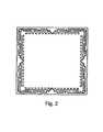
Figure 2 . This pattern is known to be very difficult to duplicate, suffers from thermal drift, and is relatively expensive to engineer and fabricate. - There is a substantial demand for a new capacitive touch screen method that is less expensive and simpler to manufacture than the above methodologies yet is highly robust and suitable for use in hostile environments. In particular there is a need for such devices in the applications of domestic appliances, mobile phones and other hand-held devices, POS terminals, and so on.
- Embodiments of the invention provide a compromise between the 'no pin cushion' but expensive circuitry and fabrication cost of prior-art striped elements, and unpatterned resistive sheet elements. This new hybrid solution produces a pin cushion effect only on one axis, leaving the other axis largely undistorted. Furthermore, as will be seen, the residual pin-cushion distortion has a largely orthogonal and predictable vector which can be compensated using relatively trivial numerical methods, is highly repeatable from unit to unit, and is more immune to differential thermal drift than the prior art.
- In
Figure 3 is shown a pattern representative of the conductive material used in a sensing element according to an embodiment of the invention. The diagram shows a single conductive element on one layer having fourelectrodes bars stripe conductors 310 traverse from bus-bar 305 to 306, numbering at least two but typically 3 or more. Two of these stripes traverse from the ends of each bus-bar to the other, thus forming a fully bounded surface. The end stripes can also be considered to be bus-bars, but as they can optionally have a higher path resistance than the horizontal bus-bars shown, they remain unique and thus will be called stripes throughout. - The element of the invention can alternatively be viewed as having a core area characterized by anisotropic conductivity with a surrounding, bounding border made from linear conductive segments. The purpose of the stripes is to force anisotropic galvanic flows within the core area. Once the current flows reach the boundary paths, they are finally led to the electrode connections.
- The number of
stripes 310 appropriate for a design depends on the width of the element in relation to the size of the object being sensed, as will be discussed below.Wires 312a-d connected to the electrodes connect the element to a drive / sensing circuit in the case of a 2DCT. In the case of a2DRT wires 312a-d are connected to a drive circuit, the sensing function coming from a flexible user-depressed cover sheet as shown inFigure 11 . Figure 10 shows another pattern embodying the invention. This pattern is substantially the same as the pattern ofFigure 3 except that the stripes are separated by thin slits (i.e. the stripes are relatively wider than those shown inFigure 3 ), so that the element is principally coated with conductive material and only a very small percentage - the slits - is uncoated. This configuration is more suitable for 2DRT use as described further below, but can also be used in 2DCT applications. One advantage of this for 2DCT use is that the stripes have larger surface areas than in theFigure 3 example, so that the capacitive coupling from finger to element is enhanced. One disadvantage of this is that the total resistance from bus-bar to bus-bar is lower for a particular sheet resistance, which will tend to exacerbate the pin cushion effect as described below.- The relative resistances of the stripes and bus-bars in
Figure 3 as tested are about 40K ohms for the bus-bars, and 160K ohms for the stripes, although in practice these figures are only for guidance and they are not limiting to the invention. The use of higher resistance value stripes than bus-bars is helpful to limit pin cushion effects, but since pin cushion is easily correctable numerically anyway, almost any combination of values will work to varying degrees of satisfaction. It is a considerable attraction of the invention that it is usable with elements having a high resistance, as such an element requires lower cost and lower power drive and sensing electronics. Figure 4 shows a lumped model of typical embodiments of the invention. Bus-bars Stripes 310 are composed of resistive lines of about 5 to 10 times more than the resistance of the bus-bars. There are 9 stripes shown inFigure 4 .Corner electrodes stray background capacitance 401 to circuit ground. Stripes havemutual capacitance 404 between neighbors. Such background capacitances are benign in nature and have been show to have no effect on the performance of the invention. These capacitances do not have to be equal or balanced for the invention to work, as the element obeys the physics of superposition, and such parasitic values are easily calibrated away by the drive electronics as will be described below.- Shown is a capacitance Ct, 402, at
position 403 due to a touch in 2DCT mode. The invention is fully tolerant of the magnitude of Ct, in that it allows the use of circuitry and / or algorithms that responds ratiometrically to the four electrode signals to derive a position independent of the magnitude of Ct. In 2DRT mode, the coversheet picks off a gradient potential, usually using time-multiplexed drive signals to the four electrodes upon galvanic connection from the coversheet to the element under the pressure of touch. - In 2DCT mode it is also possible to have a touch between stripes and to interpolate the location of touch.
Figure 5 shows the element with a touch capacitance geographically located at 403 due to finger (not shown).Figure 6 , in which is shown a cross section of the invention attached to a substrate such as glass. Thecapacitance 603 due to touch offinger 605 is split into three smaller parts, Ct1, Ct2, and Ct3 as shown inFigure 6 , whose ratio depends on the relative location of the touch among thestripes 310a,b,c.. InFigure 6 of my co-pendingUS application 60/422837 Ct 603, back through the bus-bars to the other stripe. The interpolation in the X direction is proportioned according to the resistance of the short segment of bus-bar resistance connecting the two Y stripes, as a percentage of the total electrical bus-bar 'length'. The resistance of the stripe itself is not of consequence for resolving X location, since the ends of each stripe are driven to equipotentials in most 2DCT drive circuits described in the literature, and certainly when driven by the charge-transfer circuits described in my various earlier patent publications. Thus, if the stripes are spaced apart by 10% of the total bus-bar length, then the opportunity for interpolation will be 10% of the X dimension. - Note that the element of
Figure 5 could be rotated through 90 degrees and the above discussion would have been in regard to the Y dimension. There is no preferred angle of orientation of the element of the invention with regard to detection and location of touch. The discussions and formulae noted below are based on an assumption of convenience i.e. that the stripes are aligned in a vertical, Y orientation; however, rotation of the element through 90 degrees would provide identical physical operation and the equations would still hold albeit translated through 90 degrees. Specificity in regard to the orientation in this patent is not intended except as a matter of explanatory convenience and should not be held to be limiting in any way. - The measurement circuitry, well described in the literature from a variety of inventors but preferably of any type as disclosed by the inventor in his
US patents 6,288,707 [33],6,466,036 [34] and co-pending application 60/422837 [28], is used by standard connection to the fourcorner electrodes Figure 3 with each channel being operable to generate an output signal dependent on the resistive path length between its electrode and the position of the touch. While other methods might use other formulae, the p referred method of calculation of the position of touch is an adaptation of the one disclosed in my co-pending application60/422837 - To compute the position of touch along X (i.e. the horizontal direction shown in
Figure 3 ) using the element ofFigure 3 the signals are processed according to the following steps assuming that the real time acquired signals associated with the fourelectrodes - 1) Sum the references and signals in X:


- 2) Compute the delta signals in X, i.e. ΔSigX', ΔSigX" :


- 3) Compute the ratio Px indicative of position in X:

- To compute the position of touch along Y using the element of
Figure 3 the signals are processed according to a formula similar to that indicated above: - 1) Sum the references and signals in Y:


- 2) Compute the delta signals in Y, i.e. ΔSigY', ΔSigY" :


- 3) Compute the ratio Py indicative of position in Y:

- The formula for Py can be re-expanded to:

- The complete, reported but uncorrected or 'raw' estimated position is thus (Px, Py).
- The above equations are examples only, and other equations used in conjunction with other screens may also generate a comparable result.
- In
Figure 6 is shown atouch 601 over a plurality of stripes creating a distribution of Ct over said stripes. The resultant charge flows in the element set up an areal distribution of Ct couplings across multiple stripes, roughly in proportion to the adjoining surface areas of touch and stripes. The principle of superposition applies (as it does in any sheet element) and the resultant determination of position will be properly weighted and hence located to a far higher effective resolution than the number of stripes would seem to indicate. This effect is used to greatly improve resolution in many other stripe based 2DCTs, for example inUS 4,733,222 (Evans ) [22], but whereas Evans uses numerical interpolation, the instant invention uses the physical properties of distributed capacitance among multiple stripes to achieve the same thing, without the need for further computation or for need for individual electronic addressability of each stripe. The interpolation is intrinsic to the element itself. This is an effect previously known to occur in 2DCT resistive sheet elements. Figure 7a shows the calculated position along the X axis by Y row of touch as calculated from the corner electrode signals according toEqns Figure 7b schematically represents the distortion over all quadrants of the sensing element A finger touching the element, whose circumference of contact encompasses a fractional number of stripes, shows no cogging or nonlinearity in X worth noting when dragged orthogonally to the stripes. This can be seen more graphically inFigure 8 which shows a plot of the correction vectors for 7 rows cutting across the stripes in X. At no place is there a non-orthogonal, non-vertical correction vector.- This remarkable result comes about because the stripes restrict core galvanic current flows to the stripes, which lie only along the Y axis; this restriction prevents non-orthogonal current vectors anywhere in the element. Once the current flows reach a bus-bar from a stripe, the flow rotates 90 degrees and heads towards the two nearest corner electrodes. It is only at this stage that the currents can be diverted down adjacent stripes to electrodes on the second bus-bar. This creates the pin cushion effect along the bus-bars.
Figs 7a, 7b , and8 show that in the Y axis the distortions are linear and can be corrected using a simple scaling factor which has a dependency on X. For each position in X, there exists a single scalar (non-vector) correction factor which can be use to arrive at a corrected position of touch in Y:
- Where Py is the raw reported position in Y, Pcy(x,y) is the corrected position for Y as a function of X and raw Y, and ↕(x) is a correction factor unique to each position in X for which a correction factor is sought. The coefficients ↕(x) need only be solved for in any one quadrant (for example the quadrant represented in
Figure 7a ), and the results mirrored for the other 3 quadrants. The fact that there is no non-orthogonal component to the correction, and that a single factor ↕(x) applies to any signal in Y(x), simplifies computations by two orders of magnitude over Babb so that very rapid compensation can be performed using slow, cheap microcontrollers for example costing under US$0.50. Furthermore the simplicity of the distortion and the correction method imply that the element is also more stable under fluctuating temperature or electrical conditions and is more repeatable to manufacture. Unlike Babb, the correction of the element does not require multiple trials to allow curve fitting. So long as the strip-to-bus-bar resistanceratio is repeatable (absolute stability is not required), the factors ↕(x) will be the same from one unit to the next. Inconsistencies from unit to unit will have only a limited effect on the error term in reported touch location, and errors on one axis will create only highly attenuated errors on the other axis. The element of the invention generally isolates error terms between X and Y, a non-trivial beneficial effect compared with the prior art. - The simplicity of the instant invention should be compare with the '80 coefficients' and fourth order polynomials required for Babb, the coefficients of which must be determined though an extensive calibration procedure. The instant invention may require only single point calibration, or in most cases no calibration at all, as element distortions are simple, predictable, and repeatable from unit to unit.
- The ↕(x) correction factors can be applied by means of a lookup table with interpolation to achieve a simple, fast correction. The correction factor ↕(x) can also be computed mathematically using the simple quadratic equation:

- Leading to the complete equation for Y correction:

- Where k1, k2 and k3 are coefficients that depend on the curvature of pin-cushion distortion, and X is the absolute magnitude of the position along the X axis starting from center-screen and moving in either the left or right direction. This quadratic equation was derived from simulation models and is accurate to better than 1%. It does not account for gross material nonlinearity which can be compensated for using secondary methods if required. The equations are dependent on resistance ratios between the bus-bars and the stripes as well as the geometric proportions of the element. The equations are unaffected by absolute resistance values.
- The analysis supra applies equally to a 2DCT or a 2DRT. A 2DRT generally operates in 'reverse' to a 2DCT in that the element is only driven by signals, which are then picked off by a coversheet using a 5th electrode connection for analysis purposes. The electrodes on the element proper are usually driven in a time-multiplexed mode so as to allow for unique signals to be picked up in alternating X and Y directions. For example the two left electrodes are first grounded, and the two right ones driven to a fixed and identical potential; the cover sheet is sampled to obtain a raw X position. The bottom electrodes are next grounded, and the top electrodes connected to a fixed and identical potential; the cover sheet is sampled to obtain a raw Y position. The process is repeated continuously, and a sample is declared valid only if the cover sheet is sensed to be in galvanic contact with the element This is a potentiometric pickoff method, well described in the patent literature. Other 2DRT sampling methods are possible and the sequence noted in this paragraph should not be considered a preferred method, nor is the sampling method an object of the invention.
- Equation 5 needs only a set of solutions in one quadrant, with the results mirrored for the other 3 quadrants. This is demonstrated in
figure 7a and 7b. Figure 7a shows the distortion i n the t op right quadrant; this pattern is mirrored in the other three quadrants to create the pattern of 7b. - The phenomenon of 2DCT handshadow is described in my co-pending US application
US20030132922 [37] and inUS 5,457,289 [39]. Screens that are 'mobile phone size' such as 60 x 60mm, will not generally suffer sufficiently from handshadow to warrant corrective action. - However, if desired one way to reduce the effects of handshadow is described in my aforesaid US application,
US20030132922 [37]. - A second method involves essentially repeating the element of the invention a second time as shown in
Figure 9 . However, as can be seen fromFigure 9 , this can be achieved by effectively sharing a bus-bar to reduce associated component counts. When the pattern is excited by driver/sensor circuitry on the 6 nodes (i.e. electrodes) 301, 302, 301a, 302a, 303 and 304 as shown, the element is effectively divided up in a way that allows it to be sensed in two different zones, top and bottom. Sensing within these zones is as described above. As handshadow capacitance occurs primarily below the point of touch, a touch in the upper zone will cause handshadow primarily in the lower zone, where it can be 'processed away' by simply ignoring the signals from said lower zone. There is very little cross-coupling of handshadow currents between zones. - Larger screens would make use of even more of these zones, to a number appropriate to the vertical size of the entire element and according to the severity of the problem.
Figure 10 shows an element having slits between stripes. Such a method of separating stripes is particularly useful for 2DRT usage, where a cover sheet is deflected to contact the element at a small point. If the point of contact is smaller than the gap betweenstripes 310, it can be that the coversheet fails to pick up a potential and the contact fails.Figure 11 shows a resistive screen according to the invention, wherein a cover sheet picks off a galvanic potential from the slit stripes ofFigure 10 when bent inwards via touch or via a stylus. The element offigure 11 is exactly as described above for a 2DCT, but the operating mode is according to various 5-wire screen modes a s discussed i n other patents and in the open literature. Normally the cover sheet is held apart from the element via tiny 'microbump' spacers (not shown), as is well known in the art.Figure 12 shows a minimal 2DCT case, where there are 2 bus-bars and two stripes, all on the periphery of an element. The element is of a size not significantly larger than the object being sensed, so that the signal levels in the middle do not significantly diminish due to distance from object to each conductive member. This example operates without measurable pin cushion as the impedances of the stripes and bus-bars are many orders of magnitude lower than the capacitive coupling impedance from object to any strip or bus-bar. In this minimal case, the stripes and bus-bars can have the same value or wildly differing values with minimal observable effect on resolution or linearity. If the element ofFigure 12 is for use by a human finger, the element should preferably be no more than 4 times as wide or high as the diameter of a finger in order to provide reasonable signal strengths. The element ofFigure 12 can be used to create a 'mini mouse pad' or pointer control, for example for use by those with minimal appendage mobility, whereby very small motions of a fingertip or other appendage control an appliance or GUI.- The 2DCT element is suited to use in a 'point mode' where the user simply points at the screen. The easily correctable pin cushion and use of a single element mean that fields are not localized to short distances. As a result, the invention can be used as a 'point screen' device with reasonable accuracy in most menu-based graphical interfaces.
- This mode of operation c an be extremely beneficial in hygiene applications such as in hospitals, b ut also in ordinary consumer usage modes to prevent screen smudging.
- Refer now to
Figure 13 , wherein is shown preferred (but not essential) drive circuitry for the 2DCT application of the invention. This circuit is of the same type as shown in my co-pendingUS application 60/422837 Figure 9 , etc). The repeated switching ofswitches switch controller 1307. Signal outputs are the tabulated number of switching cycles for each electrode required to exceed a threshold voltage Vt, as determined by avoltage comparator 1301. The tabulation of cycle counts for each electrode is performed by four counters at 1306. - The operation of this circuitry is explained more fully in my
US application 60/422837 - The invention can alternatively employ any of the switching sequences and topologies as described in my
US Patent 6,466,036 [34]. - Signal processing circuitry is shown in
Figure 14 , wherein the four electrode signals are input to the processing circuitry which in turn computes a coordinate result. A logic block, microcontroller, or other hardware or software is used to perform the calculations necessary to achieve the desired output. The block ofFigure 14 is usually a part of another system, such as a personal computer, process controller, appliance and so on, and the output may b e only a n intermediate result i n a larger process. Figure 15 shows a preferred embodiment of the invention wherein asingle microcontroller 1501 performs the switching functions ofFigure 13 , plus performs the signal processing ofFigure 14 . The switching functions can be performed in software on a conventional I/O port, or with an on-chip hardware capacitive conversion peripheral. Signal processing is performed in software to achieve the desired coordinate output. This output could be a mere intermediate result used to control a larger process, and the output shown may only exist as numbers inside the chip.- Alternatively the invention can use any capacitive or resistive sensing circuit described in literature. The gradient response of the element is normally the same regardless of the type of drive circuitry. The invention is not reliant on any one acquisition method.
- The 2DxT element is preferably made of a clear conductor of suitable resistance on the back of a glass or plastic sheet covering the display, if a touchscreen, or over a suitable dielectric substrate if a mousepad, etc.
- As described in various other patents, the need for low-R bus-bars (under about 200 ohms end-to-end) on the edges causes all manner of driving, power, stability, and repeatability issues. It is highly desirable to use materials with a much higher resistance than currently in widespread use. Most ITO (Indium Tin Oxide) layers such as those produced by CPFilms, USA, or when c ustom-sputtered onto a surface, have resistances around 300 ohms per square. It is highly desirable to elevate this resistance to the neighborhood of 500 to 2000 ohms per square, so that the stripe and bus-bar resistances can be made in the region of 25K ohms and up from end to end.
- One method of increasing bus-bar and stripe resistance from low resistance materials is to use a meandering path or zig-zag pattern so as to increase track length. Conventional low-resistance ITO or Tin-Oxide coatings can be etched or patterned to have intentional voids ('Swiss cheese' approach), thus raising the resistance. The stripes and bus-bars can also be made suitably thin so that the resistance is high enough to be more optimal.
- Ideal materials however will have an intrinsic resistance of about 500 to 1,000 ohms per square or more, or can be modified to become so. Agfa's Orgacon™ conductive polymer is one material that has such a high intrinsic resistance and is also clear, making it usable in touch-screens over displays. A particularly low cost material is carbon based ink, well known in the electronics trade, however being opaque this material is better suited for tablet or mousepad applications.
- The above being said, there is no requirement for any particular element resistance value, and the driving circuitry can be adapted to almost anything with varying degrees of difficulty. In theory the only requirement is that the elements have a non-zero resistance. However the bus-bar resistances should preferably be comparable or lower in value than the aggregate parallel value of the stripes in order to reduce Y-axis pin cushion. A greater number of stripes would generally m ean a higher resistance per stripe to achieve the same effect, the pin cushion being related to the total bridging resistance between stripes, the bridging resistance being the parallel equivalent value of the stripes. Stripes located towards the center of the bus-bars have a disproportionate effect on pin cushion.
- Patterning of the element into bus-bars and stripes can be via vapor deposition using a suitable stencil to prevent unwanted areas of coating, or via silk screening to create the desired pattern, or via pad-printing, or via laser scribe or chemical etching or chemical reaction, or any other process which can create a patterned layer. In the case of conductive polymer Agfa Orgacon™, the pattern can be created by using sodium hypochlorite to force areas to become non-conductive via chemical reaction without actual material removal.
- Fabrication can entail the use of normal touchscreen or touchpad methods such as vapor deposition of appropriate materials onto a glass sheet placed in front of a display.
- In-mold decorating ("IMD") entails the use of a graphic sheet or layer placed inside the injection mold or cast prior to the introduction of fluid plastic. Once molded, the layer becomes an integral part of the resultant plastic piece. In the case of a 2DCT, a conductive element of the type according to the invention is placed in the mold for a display cover; when injected, the conductive layer becomes fused to one side of the cover. In this way complex cover shapes, including those having compound curves, can be created which include an integral 2DCT at extremely low cost.
- Electrode connections can be made via wires bonded to the corners, or via conductive rubber pillars, or using metal springs, etc. Conductive rubber is a method of choice for very low cost connection from an underlying PCB containing the driver circuitry.
Figure 16 shows such a construction method in cross-section. Display 1601 is viewed throughcover lens 1602 andsensing element 300.Element 300 is connected via at least four corner electrodes through conductive rubber posts, of which two 1603a, 1603b are shown, toPCB 1604. The entire assembly is placed under compression via screws, clamps or other fastener system (not shown) so that the rubber posts are compressed and thus forced to make contact betweenPCB 1604 andelement 300. - The element can also be fabricated from molecular substances having anisotropic conduction. For example, a conductive polymer can be envisioned having conductivity that is much better in one direction than another. Such materials based on nanostructures have been described in the literature, for example in literature from Helsinki University of Technology.
- One embodiment of the invention weights the stripes so that the ones near center-screen are either spaced further apart or have a higher resistance or both. The effect of this is to reduce the amount of inherent pin cushion. However, tests have shown that while this in fact is what happens, it also means that there will be a loss of signal in the center of the element, and/or there will be drive problems through the resultant higher resistance and lower finger coupling to neighboring traces. In practice this approach is not deemed to be efficacious, and is mentioned here only for completeness.
- Problems associated with 2DCT's include interference from outside electrostatic or radio sources having a frequency at the operating frequency of the element, or some harmonic thereof. These problems can be attenuated by using a modulated operating frequency for the signal acquisition so as to reduce or prevent signal-noise aliasing or beating. This can involve the use of frequency hopping, chirps, or pseudo-random frequency modulation. These methods are known as 'spread-spectrum' modulation.
- Post processing can include the use of majority vote filtering, median filtering, averaging, and so on to reduce the residual effects of noise that are already attenuated by means of the frequency modulation.
- Low frequency interference can be caused by local mains fields and so on. This form of interference can be attenuated by synchronizing the acquisition to the interfering source, for example 50 or 60 Hz, as described in the datasheet for the Quantum Research Group Ltd (UK) QT310 device [40].
- The element is compatible with driven shield methods to reduce interference from LCD displays, VFD switching, etc. This entails the use of a conductive plane behind the element positioned between the element and the interfering source. A drive shield can also protect against signal disturbance from motion behind the element. Driven back-shields are commonly used in the construction of 2DCT's.
- In many applications it is desirable to have a 'wakeup' function, whereby the entire device 'sleeps' or is in some quiescent or background state. In such cases, it is often desirable to have a wake signal from mere proximity of a human body part some distance away.
- The element can be driven as a single large capacitive electrode without regard to position location, while the unit is in the background state. During this state the electronic driver logic looks for a very small change in signal, not necessarily enough to process as a 2D coordinate, but enough to determine that an object or human is in proximity. The electronics then 'wakes up' the overall system and the element is driven so as to become a true 2DCT once again.
- The element of the invention in 2DCT mode is suitable as a mouse pad, or as a tablet type input device. In these roles, there is no need for optical transparency. A stylus can be used with the element either to pick up a radiated electric field from the element, or to inject a signal into the element, or to act as a human finger.
- In injection mode, the element of the invention merely operates in reverse. A signal from a tethered pen is injected capacitively into the element in a region surrounding the point of contact. The signal is then apportioned ratiometrically to the four corner electrodes, from whence it can be picked up and conveyed to a measurement circuit of almost any type already described in literature and then processed to create an indicative result. The pin cushion result operates in substantially the same way in injection mode as it does in a 2DRT or 2DCT mode; the vector gradients are the same.
- Many applications do not require linearization of the result. These are principally those applications involving human interfaces of low resolution, for example for menu button sensing and the like. In such applications, the element and related signal acquisition circuitry can dispense with the linearization step and simply generate the raw output. Additional system logic would interpret 2D coordinate boundaries as being touch buttons, the boundaries being defined at the time of software development.
- If the ratio of stripe-to-bus-bar resistance is high enough, the accuracy of the raw processed result may be acceptable for direct use. For example, if the resulting coordinate error of an element is only 5% but is repeatable, the element may be perfectly suitable for uncorrected menu button detection over a display where the buttons do not occupy less than 10% of the height of the element. If the buttons are principally located near the horizontal centerline of the element, or along the left or right sides, the distortion could be negligible and if so, no linearization correction need be applied.
- The invention is at its basic reduction, an element whose purpose is to provide for an improved form of 2D sensing device via anisotropic conduction, plus, optionally, a method to correct the distortions of the raw computed coordinate result. The mode of operation (including but without limitation, galvanic or capacitive modes), the use to which it is put, and whether it is used as a receiver of signals from a stylus or a sensor of passive touch is not of prime importance to the invention. What is important is the anisotropic structure of the element and the form of positional error it produces, and the optional methods disclosed herein for correcting the error.
- An important aspect of sensing elements of embodiments of the invention is that they can be made as a single-layer having a core that conducts well galvanically in a first predetermined direction, but suppresses conduction in a second direction orthogonal to the first, i.e. it has anisotropic conductivity, plus, the core is bounded by a resistive border to make the whole element. The element furthermore has four electrodes in the corners and which are driven and/or sensed by an electronic circuit to create a resulting output indicative of touch position.
- There are many variations possible as will become evident to those skilled in the art, involving various combinations of detection methods or switch sequences outlined specifically herein. The methods disclosed herein can be combined with other methods as taught in any number of my prior patents including methods for drift compensation, calibration, moisture suppression using short switch closure times, and the like. Particular note should be made of the various possible combinations of features disclosed in my own prior art involving capacitive sensing methods, also note the capacitive products as described in the datasheets of Quantum Research G roup L td (UK), many of which have features germane to the instant invention.
- It is also possible to warp the invention into unusual shapes as disclosed by Pepper. Such transformations may prove useful in object position sensing for example in industrial settings, where location along a cylinder, sphere, or other curved surface might be important.
- It will be appreciated that although particular embodiments of the invention have been described, many modifications/additions and/or substitutions may be made within the scope of the present invention being determined by the appended claims.


Claims (36)
- A touch sensitive position sensor comprising:a substrate defining a touch sensitive platform;first and second resistive bus-bars (305; 306) arranged spaced apart on the substrate; andan anisotropic conductive (310) area having non-zero resistance arranged between the bus-bars such that currents induced in the anisotropic conductive area flow preferentially towards the bus-bars,characterized in thatthe bus-bars and anisotropic conductive area reside on a single layer, and their resistances are such that the position of a touching object can be estimated in two dimensions dependent on the resistive path length between electrodes on the bus-bars and the position of the touching object without requiring a further layer of conductive material.
- A touch sensitive position sensor according to claim 1, wherein the bus-bars each have a resistance of between 1 kQ and 50 kQ.
- A touch sensitive position sensor according to claim 1 or 2, wherein the bus-bars have substantially the same resistance.
- A touch sensitive position sensor according to any one of the preceding claims, wherein the anisotropic conductive area provides a resistance between the bus-bars of between 1 kΩ and 50 kΩ.
- A touch sensitive position sensor according to any one of the preceding claims, wherein the resistance of each of the bus-bars is less than the resistance between them provided by the anisotropic conductive area.
- A touch sensitive position sensor according to any one of claims 1 to 5, wherein the anisotropic conductive area comprises a film of molecular substance having anisotropic conduction supported on a substrate.
- A touch sensitive position sensor according to any one of claims 1 to 5, wherein the anisotropic conductive area comprises a plurality of resistive stripes connecting in parallel between the bus-bars.
- A touch sensitive position sensor according to claim 7, wherein the resistive stripes are formed from sections of resistive wire.
- A touch sensitive position sensor according to claim 7, wherein the resistive stripes are formed from a resistive material deposited on a substrate.
- A touch sensitive position sensor according to claim 7, 8 or 9, wherein the resistive stripes have widths that are greater than gaps formed between adjacent ones of the resistive stripes.
- A touch sensitive position sensor according to any one of the preceding claims, further comprising a conductive overlay separated from the anisotropic conductive area such that the conductive overlay and the anisotropic conductive area may be brought into contact by externally applied pressure.
- A touch sensitive position sensor according to any one of the preceding claims, wherein the first resistive bus-bar extends between a first and a second electrode and the first resistive bus-bar extends between a third and a fourth electrode, the position sensor further comprising first, second, third and fourth drive channels associated with respective ones of the first, second, third and fourth electrodes, each drive channel being operable to generate an output signal dependent on the resistance between its electrode and the position of the object.
- A touch sensitive position sensor according to claim 12, further comprising a processor operable to generate an estimate for the position of the object by comparing the output signals from the drive channels.
- A touch sensitive position sensor according to claim 13, wherein the processor is configured to estimate the position of the object in a first direction running between the bus-bars from a ratiometric analysis of the sum of the signals associated with the first and second electrodes and the sum of the signals associated with the third and fourth electrodes.
- A touch sensitive position sensor according to claim 13 or 14, wherein the processor is configured to estimate the position of the object in a second direction running along the bus-bars from a ratiometric analysis of the sum of the signals associated with the first and third electrodes and the sum of the signals associated with the second and fourth electrodes.
- A touch sensitive position sensor according to claim 13, 14 or 15, wherein the processor is further operable to apply a correction to the estimated position according to a pre-determined distortion associated with the platform.
- A touch sensitive position sensor according to claim 16, wherein the pre-determined distortion is a one-dimensional pin-cushion distortion.
- A touch sensitive position sensor according to any one of the preceding claims, further comprising at least one further anisotropic conductive area so as to provide a plurality of anisotropic conductive areas sharing common bus-bars.
- A touch sensitive position sensor according to any one of the preceding claims, further comprising:a third resistive bus-bar arranged on the substrate spaced apart from the second resistive bus-bar; anda further anisotropic conductive area having non-zero resistance arranged between the second and third bus-bars such that currents induced in the further anisotropic conductive area flow preferentially towards the second and third bus-bars.
- A control panel incorporating a touch sensitive position sensor according to any one of the preceding claims.
- An apparatus having a control panel according to claim 20.
- A touch sensitive position sensor according to claim 16, wherein the correction is based on scalar multiplication.
- A touch sensitive position sensor according to claim 16, wherein the correction is made by applying a correction factor, and wherein the correction factor for one direction is quadratically related to position along the other direction.
- A touch sensitive position sensor according to claim 16, wherein the correction is made by applying a correction factor obtained from a look-up table.
- A touch sensitive position sensor according to claim 12, wherein the drive channels employ charge-transfer techniques.
- A touch sensitive position sensor according to claim 25, wherein the drive channels comprise switches, and wherein corresponding switches in the respective drive channels are configured to operate at the same time during use.
- A touch sensitive position sensor according to claim 12, wherein the drive channels are provided by an appropriately programmed microcontroller.
- A touch sensitive position sensor according to claim 13, wherein the processor and the drive channels are provided by a single appropriately programmed microcontroller.
- A touch sensitive position sensor according to claim 12, wherein the electrodes are connected to the respective drive channels using conductive rubber.
- A touch sensitive position sensor according to claim 13, wherein the processor is operable to apply drift compensation.
- A touch sensitive position sensor according to claim 12, wherein the drive channels are configured to operate at a modulated frequency when acquiring data for generating the output signals.
- A touch sensitive position sensor according to claim 1, wherein the anisotropic conductive area consists of two resistive stripes, and the bus-bars and the two resistive stripes are located at the periphery of the touch sensitive platform.
- A touch sensitive position sensor according to claim 13, wherein the processor is further operable to filter acquired signals using at least one of majority vote filtering, median filtering or averaging.
- An apparatus comprising a touch sensitive position sensor according to claim 12, and further comprising a stylus operable to radiate an electric field signal for injecting into the touch sensitive position sensor, wherein the drive channels of the touch sensitive position sensor are responsive to the injected electric field so that the position of the stylus can be determined.
- A touch sensitive position according to claim 13, wherein the processor is further operable to determine when there is no object adjacent the sensing element and, in response to this, to enter a quiescent mode in which the plurality of sense channels operate together to provide a single output signal, and whereby a change in this single output causes the processor to exit the quiescent mode.
- A method of manufacturing a touch sensitive control panel comprising: introducing a touch sensitive position sensor according to claim 1 into a mold for the control panel prior to introducing fluid plastic into the mold.
Applications Claiming Priority (2)
| Application Number | Priority Date | Filing Date | Title |
|---|---|---|---|
| GB0319714AGB0319714D0 (en) | 2003-08-21 | 2003-08-21 | Anisotropic touch screen element |
| PCT/GB2004/003437WO2005020056A1 (en) | 2003-08-21 | 2004-08-09 | Anisotropic touch screen element |
Publications (2)
| Publication Number | Publication Date |
|---|---|
| EP1656608A1 EP1656608A1 (en) | 2006-05-17 |
| EP1656608B1true EP1656608B1 (en) | 2013-05-22 |
Family
ID=28460102
Family Applications (1)
| Application Number | Title | Priority Date | Filing Date |
|---|---|---|---|
| EP04768019.4AExpired - LifetimeEP1656608B1 (en) | 2003-08-21 | 2004-08-09 | Anisotropic touch screen element |
Country Status (7)
| Country | Link |
|---|---|
| US (4) | US20050041018A1 (en) |
| EP (1) | EP1656608B1 (en) |
| JP (1) | JP2007503037A (en) |
| KR (1) | KR20070011224A (en) |
| GB (1) | GB0319714D0 (en) |
| TW (1) | TWI351631B (en) |
| WO (1) | WO2005020056A1 (en) |
Families Citing this family (172)
| Publication number | Priority date | Publication date | Assignee | Title |
|---|---|---|---|---|
| GB9722766D0 (en) | 1997-10-28 | 1997-12-24 | British Telecomm | Portable computers |
| US7663607B2 (en) | 2004-05-06 | 2010-02-16 | Apple Inc. | Multipoint touchscreen |
| US7528508B2 (en) | 1998-10-09 | 2009-05-05 | Azoteq Pty Ltd. | Touch sensor user interface with compressible material construction |
| US7265494B2 (en) | 1998-10-09 | 2007-09-04 | Azoteq Pty Ltd. | Intelligent user interface with touch sensor technology |
| US6879930B2 (en)* | 2001-03-30 | 2005-04-12 | Microsoft Corporation | Capacitance touch slider |
| US6661410B2 (en)* | 2001-09-07 | 2003-12-09 | Microsoft Corporation | Capacitive sensing and data input device power management |
| US6977646B1 (en)* | 2001-11-30 | 2005-12-20 | 3M Innovative Properties Co. | Touch screen calibration system and method |
| US6954867B2 (en)* | 2002-07-26 | 2005-10-11 | Microsoft Corporation | Capacitive sensing employing a repeatable offset charge |
| US7362313B2 (en)* | 2003-01-17 | 2008-04-22 | 3M Innovative Properties Company | Touch simulation system and method |
| GB0319714D0 (en) | 2003-08-21 | 2003-09-24 | Philipp Harald | Anisotropic touch screen element |
| WO2006068782A2 (en)* | 2004-12-22 | 2006-06-29 | 3M Innovative Properties Company | Touch sensors incorporating capacitively coupled electrodes |
| DE202005001032U1 (en)* | 2005-01-22 | 2005-05-12 | Wessling, Herbert | Gaming or gambling machine, has an operating unit in the form of a dielectric operating plate that has operating fields and matching capacitive sensors on its reverse side |
| US20080170043A1 (en)* | 2005-06-10 | 2008-07-17 | Soss David A | Force-based input device |
| US20060284856A1 (en)* | 2005-06-10 | 2006-12-21 | Soss David A | Sensor signal conditioning in a force-based touch device |
| US7903090B2 (en) | 2005-06-10 | 2011-03-08 | Qsi Corporation | Force-based input device |
| US7337085B2 (en)* | 2005-06-10 | 2008-02-26 | Qsi Corporation | Sensor baseline compensation in a force-based touch device |
| US7279647B2 (en) | 2005-06-17 | 2007-10-09 | Harald Philipp | Control panel |
| US7868874B2 (en) | 2005-11-15 | 2011-01-11 | Synaptics Incorporated | Methods and systems for detecting a position-based attribute of an object using digital codes |
| US8144125B2 (en) | 2006-03-30 | 2012-03-27 | Cypress Semiconductor Corporation | Apparatus and method for reducing average scan rate to detect a conductive object on a sensing device |
| US10203814B2 (en) | 2006-04-20 | 2019-02-12 | Nokia Technologies Oy | Sensor arrangement comprising a conductive layer |
| US8279180B2 (en) | 2006-05-02 | 2012-10-02 | Apple Inc. | Multipoint touch surface controller |
| GB2437827B (en)* | 2006-05-05 | 2008-03-26 | Harald Philipp | Touch screen element |
| US8619054B2 (en) | 2006-05-31 | 2013-12-31 | Atmel Corporation | Two dimensional position sensor |
| US7830365B2 (en)* | 2006-06-07 | 2010-11-09 | Nokia Corporation | Sensors |
| US9626044B2 (en)* | 2006-06-20 | 2017-04-18 | Egalax_Empia Technology Inc. | System and method for scanning control of a capacitive touch panel |
| TW200802058A (en)* | 2006-06-20 | 2008-01-01 | Egalax Inc | Scanning control device for capacitive touch panel |
| TW200802057A (en)* | 2006-06-20 | 2008-01-01 | Egalax Inc | Compensation control method and device of a capacitive touch panel |
| US8063886B2 (en)* | 2006-07-18 | 2011-11-22 | Iee International Electronics & Engineering S.A. | Data input device |
| US20080030482A1 (en)* | 2006-07-31 | 2008-02-07 | Elwell James K | Force-based input device having an elevated contacting surface |
| US20080088595A1 (en)* | 2006-10-12 | 2008-04-17 | Hua Liu | Interconnected two-substrate layer touchpad capacitive sensing device |
| JP4916852B2 (en) | 2006-11-29 | 2012-04-18 | 株式会社 日立ディスプレイズ | LCD with touch panel |
| CN101578607B (en) | 2006-12-04 | 2013-07-17 | 德卡产品有限公司 | Medical device including a slider assembly |
| WO2008076393A1 (en)* | 2006-12-14 | 2008-06-26 | Qsi Corporation | Force-based input device having a modular sensing component |
| US8072429B2 (en) | 2006-12-22 | 2011-12-06 | Cypress Semiconductor Corporation | Multi-axial touch-sensor device with multi-touch resolution |
| US7986313B2 (en)* | 2007-01-03 | 2011-07-26 | Apple Inc. | Analog boundary scanning based on stray capacitance |
| US7920129B2 (en) | 2007-01-03 | 2011-04-05 | Apple Inc. | Double-sided touch-sensitive panel with shield and drive combined layer |
| US8144126B2 (en) | 2007-05-07 | 2012-03-27 | Cypress Semiconductor Corporation | Reducing sleep current in a capacitance sensing system |
| US20080303800A1 (en)* | 2007-05-22 | 2008-12-11 | Elwell James K | Touch-based input device providing a reconfigurable user interface |
| JP5151257B2 (en)* | 2007-06-04 | 2013-02-27 | トヨタ自動車株式会社 | Electrical equipment and method for manufacturing the same |
| US8063330B2 (en)* | 2007-06-22 | 2011-11-22 | Nokia Corporation | Uniform threshold for capacitive sensing |
| US9654104B2 (en)* | 2007-07-17 | 2017-05-16 | Apple Inc. | Resistive force sensor with capacitive discrimination |
| DE102007034273A1 (en)* | 2007-07-19 | 2009-01-22 | Volkswagen Ag | Method for determining the position of a user's finger in a motor vehicle and position determining device |
| GB2451267A (en)* | 2007-07-26 | 2009-01-28 | Harald Philipp | Capacitive position sensor |
| US7808490B2 (en)* | 2007-08-29 | 2010-10-05 | Egalax—Empia Technology Inc. | Device and method for determining touch position on sensing area of capacitive touch panel |
| US8248081B2 (en)* | 2007-09-06 | 2012-08-21 | Cypress Semiconductor Corporation | Calibration of single-layer touch-sensor device |
| EP2193693A4 (en)* | 2007-09-17 | 2014-01-01 | Magna Int Inc | KEYBOARD WITHOUT KEYS AND WITHOUT INTEGRATED PRESSURE Ä BACKLIGHT LIGHT EMITTING |
| EP2790088B1 (en) | 2007-09-18 | 2019-05-01 | Senseg Oy | Method and apparatus for sensory stimulation |
| FI20085475A0 (en)* | 2008-05-19 | 2008-05-19 | Senseg Oy | Touch Device Interface |
| TW200917111A (en)* | 2007-10-02 | 2009-04-16 | Himark Technology Inc | Resistive type multi-touch control panel and its detection method |
| US8059103B2 (en)* | 2007-11-21 | 2011-11-15 | 3M Innovative Properties Company | System and method for determining touch positions based on position-dependent electrical charges |
| WO2009078391A1 (en)* | 2007-12-14 | 2009-06-25 | Kyocera Corporation | Touch panel and touch panel display device |
| US20090153494A1 (en)* | 2007-12-18 | 2009-06-18 | Kevin Scott Laundroche | Touch display for an appliance |
| TWI374379B (en) | 2007-12-24 | 2012-10-11 | Wintek Corp | Transparent capacitive touch panel and manufacturing method thereof |
| US20090174675A1 (en)* | 2008-01-09 | 2009-07-09 | Dave Gillespie | Locating multiple objects on a capacitive touch pad |
| US8284332B2 (en)* | 2008-08-01 | 2012-10-09 | 3M Innovative Properties Company | Touch screen sensor with low visibility conductors |
| KR101720919B1 (en)* | 2008-02-28 | 2017-03-28 | 쓰리엠 이노베이티브 프로퍼티즈 컴파니 | Touch screen sensor |
| CN102016766B (en) | 2008-02-28 | 2014-05-14 | 3M创新有限公司 | Touch screen sensor with low visibility conductors |
| EP2863295B1 (en) | 2008-02-28 | 2019-10-16 | 3M Innovative Properties Company | Touch screen sensor having varying sheet resistance |
| CN102017071B (en) | 2008-02-28 | 2013-12-18 | 3M创新有限公司 | Method of patterning a conductor on a substrate |
| DE102009019910B4 (en) | 2008-05-01 | 2021-09-16 | Solas Oled Ltd. | Gesture recognition |
| US8526767B2 (en)* | 2008-05-01 | 2013-09-03 | Atmel Corporation | Gesture recognition |
| JP5154316B2 (en) | 2008-06-30 | 2013-02-27 | 株式会社ジャパンディスプレイイースト | Touch panel |
| US8228306B2 (en)* | 2008-07-23 | 2012-07-24 | Flextronics Ap, Llc | Integration design for capacitive touch panels and liquid crystal displays |
| US9128568B2 (en)* | 2008-07-30 | 2015-09-08 | New Vision Display (Shenzhen) Co., Limited | Capacitive touch panel with FPC connector electrically coupled to conductive traces of face-to-face ITO pattern structure in single plane |
| TWI375901B (en)* | 2008-08-05 | 2012-11-01 | Elan Microelectronics Corp | Touch screen and method for positioning coordinate |
| KR100982282B1 (en)* | 2008-09-19 | 2010-09-15 | 주식회사 애트랩 | Sensor, sensor sensing method, and sensor filter |
| US9927924B2 (en) | 2008-09-26 | 2018-03-27 | Apple Inc. | Differential sensing for a touch panel |
| JP5370723B2 (en)* | 2008-09-29 | 2013-12-18 | 株式会社ジャパンディスプレイ | Capacitance type input device, display device with input function, and electronic device |
| KR101497419B1 (en)* | 2008-11-10 | 2015-03-02 | 위순임 | Touchscreen device having conductive sensing-net of two dimensions |
| KR101497416B1 (en)* | 2008-11-15 | 2015-03-02 | 위순임 | Touch screen device with two-dimensional conductive sensing network |
| US8183875B2 (en)* | 2008-11-26 | 2012-05-22 | 3M Innovative Properties Company | System and method for determining touch positions based on passively-induced position-dependent electrical charges |
| US8209861B2 (en) | 2008-12-05 | 2012-07-03 | Flextronics Ap, Llc | Method for manufacturing a touch screen sensor assembly |
| US8274486B2 (en)* | 2008-12-22 | 2012-09-25 | Flextronics Ap, Llc | Diamond pattern on a single layer |
| US20100156811A1 (en)* | 2008-12-22 | 2010-06-24 | Ding Hua Long | New pattern design for a capacitive touch screen |
| US20100156846A1 (en)* | 2008-12-23 | 2010-06-24 | Flextronics Ap, Llc | Single substrate capacitive touch panel |
| JP2010186460A (en)* | 2009-01-19 | 2010-08-26 | Panasonic Corp | Touch panel |
| US8508492B2 (en)* | 2009-01-19 | 2013-08-13 | Panasonic Corporation | Touch panel and method of detecting press operation position thereon |
| US9740341B1 (en) | 2009-02-26 | 2017-08-22 | Amazon Technologies, Inc. | Capacitive sensing with interpolating force-sensitive resistor array |
| US10180746B1 (en) | 2009-02-26 | 2019-01-15 | Amazon Technologies, Inc. | Hardware enabled interpolating sensor and display |
| US20100214225A1 (en)* | 2009-02-26 | 2010-08-26 | Research In Motion Limited | Method for and apparatus for display scrolling |
| US20100220063A1 (en)* | 2009-02-27 | 2010-09-02 | Panasonic Corporation | System and methods for calibratable translation of position |
| KR101666489B1 (en)* | 2009-03-26 | 2016-10-14 | (주) 엔피홀딩스 | Touchscreen device having conductive sensing-net of two dimensions |
| US8174510B2 (en) | 2009-03-29 | 2012-05-08 | Cypress Semiconductor Corporation | Capacitive touch screen |
| TWI398807B (en)* | 2009-04-07 | 2013-06-11 | Ite Tech Inc | Posistion apparatus for touch device and posistion method thereof |
| TWI466004B (en) | 2009-04-17 | 2014-12-21 | Egalax Empia Technology Inc | Method and device for resistive multi-point touch |
| US8547345B2 (en)* | 2009-05-04 | 2013-10-01 | Microsoft Corporation | Touch sensitive LCD panel |
| US8976122B2 (en)* | 2009-06-24 | 2015-03-10 | Egalax—Empia Technology Inc. | Control unit, sensing device for a capacitive touch panel and method therefor |
| CN101943978B (en)* | 2009-07-06 | 2012-12-26 | 弗莱克斯电子有限责任公司 | Capacitive touch screen panel and its manufacturing method, and capacitive touch sensor |
| CN101943975B (en)* | 2009-07-09 | 2015-12-16 | 敦泰科技有限公司 | Ultra-thin mutual capacitance touch screen and combined ultra-thin touch screen |
| CN101950213B (en)* | 2009-07-10 | 2013-05-22 | 群康科技(深圳)有限公司 | Touch screen and multi-point identification method used for same |
| TWI395998B (en)* | 2009-07-15 | 2013-05-11 | Innolux Corp | Conductive plate and touch plate applied by the same |
| US9753597B2 (en) | 2009-07-24 | 2017-09-05 | Cypress Semiconductor Corporation | Mutual capacitance sensing array |
| US20110018829A1 (en)* | 2009-07-24 | 2011-01-27 | Cypress Semiconductor Corporation | Mutual capacitance sensing array |
| US9785272B1 (en) | 2009-07-31 | 2017-10-10 | Amazon Technologies, Inc. | Touch distinction |
| US9740340B1 (en) | 2009-07-31 | 2017-08-22 | Amazon Technologies, Inc. | Visually consistent arrays including conductive mesh |
| CN101995988B (en)* | 2009-08-19 | 2012-08-15 | 群康科技(深圳)有限公司 | Touch screen |
| US8791907B2 (en) | 2009-08-19 | 2014-07-29 | U-Pixel Technologies Inc. | Touch sensing apparatus and method using different modulated driving signals |
| TWI394069B (en)* | 2009-09-08 | 2013-04-21 | Au Optronics Corp | Touch-sensing structure for touch panel and touch-sensing method thereof |
| TWI512553B (en)* | 2009-09-21 | 2015-12-11 | Silicon Integrated Sys Corp | Touch sensing apparatus and method |
| KR101191117B1 (en)* | 2009-09-28 | 2012-10-15 | 주식회사 엘지화학 | Touch panel |
| WO2011041944A1 (en) | 2009-10-09 | 2011-04-14 | 禾瑞亚科技股份有限公司 | Method and device for dual-differential sensing |
| US8842079B2 (en) | 2009-10-09 | 2014-09-23 | Egalax—Empia Technology Inc. | Method and device for determining a touch or touches |
| US8400422B2 (en) | 2009-10-09 | 2013-03-19 | Egalax—Empia Technology Inc. | Method and device for analyzing positions |
| US20110102331A1 (en)* | 2009-10-29 | 2011-05-05 | Qrg Limited | Redundant touchscreen electrodes |
| US8766933B2 (en)* | 2009-11-12 | 2014-07-01 | Senseg Ltd. | Tactile stimulation apparatus having a composite section comprising a semiconducting material |
| US8810524B1 (en) | 2009-11-20 | 2014-08-19 | Amazon Technologies, Inc. | Two-sided touch sensor |
| US9298303B2 (en)* | 2009-12-31 | 2016-03-29 | Google Technology Holdings LLC | Duty cycle modulation of periodic time-synchronous receivers for noise reduction |
| CN102193692B (en)* | 2010-03-03 | 2014-09-10 | 群康科技(深圳)有限公司 | Surface capacitive touch panel and display device, electronic device as well as driving method thereof |
| TWI413928B (en)* | 2010-03-17 | 2013-11-01 | Innolux Corp | Touch panel and differential detection method for same |
| US9285929B2 (en) | 2010-03-30 | 2016-03-15 | New Vision Display (Shenzhen) Co., Limited | Touchscreen system with simplified mechanical touchscreen design using capacitance and acoustic sensing technologies, and method therefor |
| KR101109382B1 (en)* | 2010-04-12 | 2012-01-30 | 삼성전기주식회사 | Touch panel |
| US8941395B2 (en) | 2010-04-27 | 2015-01-27 | 3M Innovative Properties Company | Integrated passive circuit elements for sensing devices |
| US9203489B2 (en) | 2010-05-05 | 2015-12-01 | Google Technology Holdings LLC | Method and precoder information feedback in multi-antenna wireless communication systems |
| US20110273372A1 (en)* | 2010-05-09 | 2011-11-10 | Elsid Aliaj | Mobile device with unique features |
| US9164620B2 (en)* | 2010-06-07 | 2015-10-20 | Apple Inc. | Touch sensing error compensation |
| US9557837B2 (en)* | 2010-06-15 | 2017-01-31 | Pixart Imaging Inc. | Touch input apparatus and operation method thereof |
| JP5427126B2 (en)* | 2010-07-01 | 2014-02-26 | アルパイン株式会社 | Electronic device and touch panel calibration method |
| WO2012012299A2 (en) | 2010-07-21 | 2012-01-26 | Synaptics Incorporated | Producing capacitive images comprising non-connection values |
| US20120038577A1 (en)* | 2010-08-16 | 2012-02-16 | Floatingtouch, Llc | Floating plane touch input device and method |
| DE102010044820B4 (en)* | 2010-09-09 | 2015-01-22 | Ident Technology Ag | Sensor device and method for approach and touch detection |
| TW201218028A (en) | 2010-10-26 | 2012-05-01 | Novatek Microelectronics Corp | Coordinates algorithm of touch panel |
| US20120105325A1 (en)* | 2010-10-27 | 2012-05-03 | Avago Technologies Ecbu Ip (Singapore) Pte. Ltd. | Capacitive finger navigation input device |
| CN102478988B (en)* | 2010-11-26 | 2014-10-15 | 群康科技(深圳)有限公司 | Method for detecting touch point on touch screen |
| CN103250350A (en) | 2010-11-30 | 2013-08-14 | 瑟克公司 | Linear projected single-layer capacitance sensor |
| WO2012108911A1 (en) | 2011-02-07 | 2012-08-16 | Cypress Semiconductor Corporation | Noise filtering devices, systems and methods for capacitance sensing devices |
| TWI459267B (en)* | 2011-04-26 | 2014-11-01 | Shih Hua Technology Ltd | Method for detecting touch spot of touch panel |
| TWI447635B (en)* | 2011-04-29 | 2014-08-01 | Shih Hua Technology Ltd | Method for detecting touch trace based on resistive touch panel |
| TWI454978B (en)* | 2011-05-02 | 2014-10-01 | Shih Hua Technology Ltd | Touching based input device |
| TWI453649B (en)* | 2011-05-02 | 2014-09-21 | Shih Hua Technology Ltd | Display device with touch panel |
| TWI461997B (en)* | 2011-05-25 | 2014-11-21 | Innolux Corp | Method and apparatus for driving a touch panel with an anisotropic material and touch panel module |
| TWI585658B (en)* | 2011-06-03 | 2017-06-01 | 識驊科技股份有限公司 | Method for detecting touch spot of touch panel |
| FR2976688B1 (en) | 2011-06-16 | 2021-04-23 | Nanotec Solution | DEVICE AND METHOD FOR GENERATING AN ELECTRICAL POWER SUPPLY IN AN ELECTRONIC SYSTEM WITH A VARIABLE REFERENCE POTENTIAL. |
| US20130018489A1 (en)* | 2011-07-14 | 2013-01-17 | Grunthaner Martin Paul | Combined force and proximity sensing |
| CN102999193B (en)* | 2011-09-13 | 2016-01-13 | 天津富纳源创科技有限公司 | The detection method of touch screen touch point |
| US20130100041A1 (en)* | 2011-10-21 | 2013-04-25 | Touch Turns Llc | System for a single-layer sensor having reduced number of interconnect pads for the interconnect periphery of the sensor panel |
| TW201319921A (en)* | 2011-11-07 | 2013-05-16 | Benq Corp | Method for screen control and method for screen display on a touch screen |
| TWI455003B (en)* | 2011-11-25 | 2014-10-01 | Shih Hua Technology Ltd | Capacitive touch panel and driving method for preventing leakage current of the capacitive touch panel. |
| FR2985049B1 (en) | 2011-12-22 | 2014-01-31 | Nanotec Solution | CAPACITIVE MEASURING DEVICE WITH SWITCHED ELECTRODES FOR TOUCHLESS CONTACTLESS INTERFACES |
| US8525955B2 (en) | 2012-01-31 | 2013-09-03 | Multek Display (Hong Kong) Limited | Heater for liquid crystal display |
| JP5830396B2 (en)* | 2012-01-31 | 2015-12-09 | 富士通コンポーネント株式会社 | Position detection method for touch panel and touch panel |
| US9444452B2 (en) | 2012-02-24 | 2016-09-13 | Parade Technologies, Ltd. | Frequency hopping algorithm for capacitance sensing devices |
| TWI456470B (en)* | 2012-03-07 | 2014-10-11 | Himax Tech Ltd | Touch cell applied to capacitive touch panel and associated capacitive touch panel |
| JP5224203B1 (en) | 2012-07-11 | 2013-07-03 | 大日本印刷株式会社 | Touch panel sensor, touch panel device, and display device |
| WO2014015032A2 (en) | 2012-07-19 | 2014-01-23 | Cypress Semiconductor Corporation | Touchscreen data processing |
| US8988387B2 (en)* | 2012-08-02 | 2015-03-24 | Google Technology Holdings LLC | Touch sensor panel with in-plane backup bypass connections |
| US9813262B2 (en) | 2012-12-03 | 2017-11-07 | Google Technology Holdings LLC | Method and apparatus for selectively transmitting data using spatial diversity |
| US9591508B2 (en) | 2012-12-20 | 2017-03-07 | Google Technology Holdings LLC | Methods and apparatus for transmitting data between different peer-to-peer communication groups |
| US9979531B2 (en) | 2013-01-03 | 2018-05-22 | Google Technology Holdings LLC | Method and apparatus for tuning a communication device for multi band operation |
| US9921668B1 (en)* | 2013-01-25 | 2018-03-20 | Qualcomm Incorporated | Touch panel controller integrated with host processor for dynamic baseline image update |
| US10229697B2 (en) | 2013-03-12 | 2019-03-12 | Google Technology Holdings LLC | Apparatus and method for beamforming to obtain voice and noise signals |
| US9360973B2 (en)* | 2013-06-26 | 2016-06-07 | Tianjin Funayuanchuang Technology Co., Ltd. | Method and apparatus for determining touch point coordinates on a touch panel with anisotropic films |
| US11265444B2 (en) | 2013-08-23 | 2022-03-01 | Preemadonna Inc. | Apparatus for applying coating to nails |
| US9687059B2 (en) | 2013-08-23 | 2017-06-27 | Preemadonna Inc. | Nail decorating apparatus |
| US9386542B2 (en) | 2013-09-19 | 2016-07-05 | Google Technology Holdings, LLC | Method and apparatus for estimating transmit power of a wireless device |
| US9007343B1 (en) | 2013-10-01 | 2015-04-14 | Synaptics Incorporated | Display guarding techniques |
| CN104679308A (en)* | 2013-11-28 | 2015-06-03 | 天津富纳源创科技有限公司 | Control method of touch screen |
| US9549290B2 (en) | 2013-12-19 | 2017-01-17 | Google Technology Holdings LLC | Method and apparatus for determining direction information for a wireless device |
| US9491007B2 (en) | 2014-04-28 | 2016-11-08 | Google Technology Holdings LLC | Apparatus and method for antenna matching |
| US9478847B2 (en) | 2014-06-02 | 2016-10-25 | Google Technology Holdings LLC | Antenna system and method of assembly for a wearable electronic device |
| JP2017521225A (en)* | 2014-07-23 | 2017-08-03 | プリマドンナ, インコーポレイテッドPreemadonna Inc. | Equipment for applying coatings to nails |
| US9857925B2 (en)* | 2014-09-30 | 2018-01-02 | Synaptics Incorporated | Combining sensor electrodes in a matrix sensor |
| CN105607791A (en) | 2014-11-13 | 2016-05-25 | 财团法人工业技术研究院 | Lead structure and sensing element |
| JP6545453B2 (en) | 2014-12-02 | 2019-07-17 | 富士通コンポーネント株式会社 | Touch panel device and coordinate correction method for touch panel |
| DE102014225235A1 (en)* | 2014-12-09 | 2016-06-09 | Siemens Healthcare Gmbh | Circuit arrangement with a resistive touch screen, medical imaging device with a resistive touch screen and method for operating a resistive touch screen |
| TW201631716A (en)* | 2015-02-16 | 2016-09-01 | Xintec Inc | A chip scale sensing chip package module and a manufacturing method thereof |
| CN105630264B (en)* | 2016-02-22 | 2019-01-18 | 京东方科技集团股份有限公司 | Touch base plate and production method, driving device and driving method, display device |
| JP6297613B2 (en)* | 2016-03-22 | 2018-03-20 | Nissha株式会社 | Pressure sensor |
| TWI661348B (en)* | 2017-05-11 | 2019-06-01 | 禾瑞亞科技股份有限公司 | Touch sensitive processing apparatus, system and method thereof |
| WO2019070886A1 (en) | 2017-10-04 | 2019-04-11 | Preemadonna Inc. | Systems and methods of adaptive nail printing and collaborative beauty platform hosting |
| WO2021015401A1 (en)* | 2019-07-24 | 2021-01-28 | Samsung Electronics Co., Ltd. | Touch detection and position reconstruction |
| US11068116B2 (en) | 2019-07-24 | 2021-07-20 | Samsung Electronics Company, Ltd. | Touch detection and position reconstruction |
| GB2602264B (en)* | 2020-12-17 | 2024-12-18 | Peratech Ip Ltd | Calibration of a force sensing device |
Family Cites Families (83)
| Publication number | Priority date | Publication date | Assignee | Title |
|---|---|---|---|---|
| DE203719C (en) | 1907-11-02 | 1908-10-20 | ||
| US645251A (en)* | 1899-09-05 | 1900-03-13 | Charles F Dittmar | Child's carriage. |
| US2338949A (en)* | 1939-10-16 | 1944-01-11 | Kupfmuller Karl | Telautograph |
| US2925467A (en)* | 1958-10-31 | 1960-02-16 | Bell Telephone Labor Inc | Electrographic transmitter |
| GB1280341A (en)* | 1969-03-13 | 1972-07-05 | Automatic Radio Mfg Co | Improvements in and relating to position responsive apparatus |
| US3921166A (en)* | 1972-09-15 | 1975-11-18 | Raytheon Co | Capacitance matrix keyboard |
| US4198539A (en)* | 1977-01-19 | 1980-04-15 | Peptek, Inc. | System for producing electric field with predetermined characteristics and edge terminations for resistance planes therefor |
| US4371746A (en)* | 1978-01-05 | 1983-02-01 | Peptek, Incorporated | Edge terminations for impedance planes |
| US4293734A (en)* | 1979-02-23 | 1981-10-06 | Peptek, Incorporated | Touch panel system and method |
| US4686332A (en)* | 1986-06-26 | 1987-08-11 | International Business Machines Corporation | Combined finger touch and stylus detection system for use on the viewing surface of a visual display device |
| US4733222A (en)* | 1983-12-27 | 1988-03-22 | Integrated Touch Arrays, Inc. | Capacitance-variation-sensitive touch sensing array system |
| AU552619B2 (en)* | 1984-02-29 | 1986-06-12 | Fujitsu Limited | Co-ordinate detecting apparatus |
| US4650926A (en)* | 1984-10-26 | 1987-03-17 | Scriptel Corporation | Electrographic system and method |
| US4622437A (en)* | 1984-11-29 | 1986-11-11 | Interaction Systems, Inc. | Method and apparatus for improved electronic touch mapping |
| US4822957B1 (en)* | 1984-12-24 | 1996-11-19 | Elographics Inc | Electrographic touch sensor having reduced bow of equipotential field lines therein |
| US4649232A (en)* | 1985-06-07 | 1987-03-10 | Scriptel Corporation | Electrographic apparatus |
| US4678869A (en)* | 1985-10-25 | 1987-07-07 | Scriptel Corporation | Position responsive apparatus, system and method having electrographic application |
| JPH0191350A (en) | 1987-09-30 | 1989-04-11 | Showa Alum Corp | Surface treatment of aluminum alloy cylinder for tape recorder |
| US4827084A (en)* | 1987-11-19 | 1989-05-02 | Ovonic Imaging Systems, Inc. | Solid state image detector and signal generator |
| JPH0237413A (en)* | 1988-07-27 | 1990-02-07 | Oki Electric Ind Co Ltd | Coordinate input device |
| US4963702A (en)* | 1989-02-09 | 1990-10-16 | Interlink Electronics, Inc. | Digitizer pad featuring spacial definition of a pressure contact area |
| US5305017A (en)* | 1989-08-16 | 1994-04-19 | Gerpheide George E | Methods and apparatus for data input |
| EP0435438B1 (en)* | 1989-12-28 | 1998-03-04 | Gunze Limited | Input system including resistance film touch panel |
| US5149919A (en)* | 1990-10-31 | 1992-09-22 | International Business Machines Corporation | Stylus sensing system |
| US5157227A (en)* | 1991-01-17 | 1992-10-20 | Summagraphics Corporation | Digitizer tablet with regional error correction |
| US5101081A (en)* | 1991-03-25 | 1992-03-31 | Wang Laboratories, Inc. | Graphics surface assembly with calibrating memory device |
| US5381160A (en)* | 1991-09-27 | 1995-01-10 | Calcomp Inc. | See-through digitizer with clear conductive grid |
| JP3190407B2 (en)* | 1992-02-27 | 2001-07-23 | グンゼ株式会社 | Touch panel device |
| JPH05265633A (en)* | 1992-03-18 | 1993-10-15 | Gunze Ltd | Touch panel |
| US5914465A (en)* | 1992-06-08 | 1999-06-22 | Synaptics, Inc. | Object position detector |
| US5463388A (en)* | 1993-01-29 | 1995-10-31 | At&T Ipm Corp. | Computer mouse or keyboard input device utilizing capacitive sensors |
| BE1007462A3 (en)* | 1993-08-26 | 1995-07-04 | Philips Electronics Nv | Data processing device with touch sensor and power. |
| US5945639A (en)* | 1994-02-04 | 1999-08-31 | Hyundai Electronics America | Cancellation of common-mode signals in digitizing tablet |
| US5457289A (en)* | 1994-03-16 | 1995-10-10 | Microtouch Systems, Inc. | Frontally shielded capacitive touch sensor system |
| GB9406702D0 (en)* | 1994-04-05 | 1994-05-25 | Binstead Ronald P | Multiple input proximity detector and touchpad system |
| TW274598B (en)* | 1994-11-15 | 1996-04-21 | Alps Electric Co Ltd | Coordinate input device for pen of finger tip |
| JP3825487B2 (en)* | 1995-03-03 | 2006-09-27 | 日本写真印刷株式会社 | Transparent touch panel |
| US5730165A (en)* | 1995-12-26 | 1998-03-24 | Philipp; Harald | Time domain capacitive field detector |
| US5682032A (en)* | 1996-02-22 | 1997-10-28 | Philipp; Harald | Capacitively coupled identity verification and escort memory apparatus |
| US5940065A (en)* | 1996-03-15 | 1999-08-17 | Elo Touchsystems, Inc. | Algorithmic compensation system and method therefor for a touch sensor panel |
| US5815141A (en)* | 1996-04-12 | 1998-09-29 | Elo Touch Systems, Inc. | Resistive touchscreen having multiple selectable regions for pressure discrimination |
| KR100382061B1 (en)* | 1996-04-16 | 2003-07-12 | 삼성에스디아이 주식회사 | Finger touch panel input device |
| JPH09293428A (en)* | 1996-04-26 | 1997-11-11 | Fujikura Ltd | Membrane switch |
| JPH09305291A (en)* | 1996-05-17 | 1997-11-28 | Fujitsu Takamizawa Component Kk | Touch input panel |
| US6288707B1 (en)* | 1996-07-29 | 2001-09-11 | Harald Philipp | Capacitive position sensor |
| US5943044A (en)* | 1996-08-05 | 1999-08-24 | Interlink Electronics | Force sensing semiconductive touchpad |
| JPH1091350A (en)* | 1996-09-10 | 1998-04-10 | Tokyo Cosmos Electric Co Ltd | Touch panel |
| US5818430A (en)* | 1997-01-24 | 1998-10-06 | C.A.M. Graphics Co., Inc. | Touch screen |
| JP3221368B2 (en)* | 1997-09-17 | 2001-10-22 | 日本電気株式会社 | Resistive tablet, control method therefor, and recording medium storing program for realizing the method |
| US6016140A (en)* | 1997-10-29 | 2000-01-18 | Nortel Networks Corporation | Automatic touch screen calibration |
| US7663607B2 (en)* | 2004-05-06 | 2010-02-16 | Apple Inc. | Multipoint touchscreen |
| US6429846B2 (en)* | 1998-06-23 | 2002-08-06 | Immersion Corporation | Haptic feedback for touchpads and other touch controls |
| US6057903A (en)* | 1998-08-18 | 2000-05-02 | International Business Machines Corporation | Liquid crystal display device employing a guard plane between a layer for measuring touch position and common electrode layer |
| US6466036B1 (en)* | 1998-11-25 | 2002-10-15 | Harald Philipp | Charge transfer capacitance measurement circuit |
| US6535200B2 (en)* | 1999-01-25 | 2003-03-18 | Harald Philipp | Capacitive position sensor |
| US6452514B1 (en)* | 1999-01-26 | 2002-09-17 | Harald Philipp | Capacitive sensor and array |
| AU4419800A (en)* | 1999-05-20 | 2000-12-12 | Electrotextiles Company Limited | Detector constructed from fabric |
| KR100473592B1 (en)* | 1999-07-19 | 2005-03-07 | 엘지.필립스 엘시디 주식회사 | A digitizer |
| US6504530B1 (en)* | 1999-09-07 | 2003-01-07 | Elo Touchsystems, Inc. | Touch confirming touchscreen utilizing plural touch sensors |
| US20040207606A1 (en)* | 1999-11-08 | 2004-10-21 | Atwood Stephen P. | Sensing the size of a touch point in a touch-sensitive panel employing resistive membranes |
| JP4550251B2 (en)* | 2000-09-29 | 2010-09-22 | 日本写真印刷株式会社 | Narrow frame touch panel |
| US6593916B1 (en)* | 2000-11-03 | 2003-07-15 | James L. Aroyan | Touchscreen having multiple parallel connections to each electrode in a series resistor chain on the periphery of the touch area |
| JP3764865B2 (en)* | 2000-11-06 | 2006-04-12 | 日本写真印刷株式会社 | Touch panel capable of wide-area input |
| GB2371910A (en)* | 2001-01-31 | 2002-08-07 | Seiko Epson Corp | Display devices |
| JP3815239B2 (en)* | 2001-03-13 | 2006-08-30 | 日本電気株式会社 | Semiconductor device mounting structure and printed wiring board |
| US20030132922A1 (en)* | 2002-01-17 | 2003-07-17 | Harald Philipp | Touch screen detection apparatus |
| US6933931B2 (en)* | 2002-08-23 | 2005-08-23 | Ceronix, Inc. | Method and apparatus of position location |
| US7180508B2 (en)* | 2002-09-17 | 2007-02-20 | Tyco Electronics Corporation | Dynamic corrections for a non-linear touchscreen |
| JP4239197B2 (en) | 2003-06-25 | 2009-03-18 | 和光工業株式会社 | SLIDE FRAME DRIVE DEVICE FOR VEHICLE OBTAINMENT |
| GB0319714D0 (en)* | 2003-08-21 | 2003-09-24 | Philipp Harald | Anisotropic touch screen element |
| EP1746488A2 (en) | 2005-07-21 | 2007-01-24 | TPO Displays Corp. | Electromagnetic digitizer sensor array structure |
| US8031174B2 (en) | 2007-01-03 | 2011-10-04 | Apple Inc. | Multi-touch surface stackup arrangement |
| US7920129B2 (en)* | 2007-01-03 | 2011-04-05 | Apple Inc. | Double-sided touch-sensitive panel with shield and drive combined layer |
| US8049732B2 (en) | 2007-01-03 | 2011-11-01 | Apple Inc. | Front-end signal compensation |
| US8040326B2 (en) | 2007-06-13 | 2011-10-18 | Apple Inc. | Integrated in-plane switching display and touch sensor |
| KR101720919B1 (en) | 2008-02-28 | 2017-03-28 | 쓰리엠 이노베이티브 프로퍼티즈 컴파니 | Touch screen sensor |
| JP4720857B2 (en) | 2008-06-18 | 2011-07-13 | ソニー株式会社 | Capacitance type input device and display device with input function |
| US8031094B2 (en) | 2009-09-11 | 2011-10-04 | Apple Inc. | Touch controller with improved analog front end |
| US9866660B2 (en) | 2011-03-21 | 2018-01-09 | Apple Inc. | Electronic devices with concave displays |
| US8934228B2 (en) | 2011-03-21 | 2015-01-13 | Apple Inc. | Display-based speaker structures for electronic devices |
| WO2012129247A2 (en) | 2011-03-21 | 2012-09-27 | Apple Inc. | Electronic devices with flexible displays |
| US8816977B2 (en) | 2011-03-21 | 2014-08-26 | Apple Inc. | Electronic devices with flexible displays |
| US9178970B2 (en) | 2011-03-21 | 2015-11-03 | Apple Inc. | Electronic devices with convex displays |
- 2003
- 2003-08-21GBGB0319714Apatent/GB0319714D0/ennot_activeCeased
- 2004
- 2004-08-09WOPCT/GB2004/003437patent/WO2005020056A1/enactiveApplication Filing
- 2004-08-09KRKR1020067003559Apatent/KR20070011224A/ennot_activeWithdrawn
- 2004-08-09JPJP2006523671Apatent/JP2007503037A/enactivePending
- 2004-08-09EPEP04768019.4Apatent/EP1656608B1/ennot_activeExpired - Lifetime
- 2004-08-12USUS10/916,759patent/US20050041018A1/ennot_activeAbandoned
- 2004-08-16TWTW93124578Apatent/TWI351631B/ennot_activeIP Right Cessation
- 2006
- 2006-06-07USUS11/422,799patent/US7825905B2/ennot_activeExpired - Fee Related
- 2010
- 2010-10-29USUS12/915,730patent/US8049738B2/ennot_activeExpired - Fee Related
- 2011
- 2011-10-31USUS13/286,153patent/US8847900B2/ennot_activeExpired - Lifetime
Also Published As
| Publication number | Publication date |
|---|---|
| TW200529052A (en) | 2005-09-01 |
| US20050041018A1 (en) | 2005-02-24 |
| US8049738B2 (en) | 2011-11-01 |
| EP1656608A1 (en) | 2006-05-17 |
| GB0319714D0 (en) | 2003-09-24 |
| US20110043482A1 (en) | 2011-02-24 |
| US7825905B2 (en) | 2010-11-02 |
| TWI351631B (en) | 2011-11-01 |
| JP2007503037A (en) | 2007-02-15 |
| US8847900B2 (en) | 2014-09-30 |
| WO2005020056A1 (en) | 2005-03-03 |
| KR20070011224A (en) | 2007-01-24 |
| US20120044206A1 (en) | 2012-02-23 |
| US20060207806A1 (en) | 2006-09-21 |
Similar Documents
| Publication | Publication Date | Title |
|---|---|---|
| EP1656608B1 (en) | Anisotropic touch screen element | |
| CA2396763C (en) | Touchscreen having multiple parallel connections to each electrode in a series resistor chain on the periphery of the touch area | |
| US9411481B2 (en) | Hybrid capacitive touch screen element | |
| US8619054B2 (en) | Two dimensional position sensor | |
| US7180508B2 (en) | Dynamic corrections for a non-linear touchscreen | |
| TWI424337B (en) | Two-dimensional position sensor | |
| US10126883B2 (en) | Capacitive touch panel with height determination function | |
| US20060227114A1 (en) | Touch location determination with error correction for sensor movement | |
| US20150286321A1 (en) | Linear projected single-layer capacitance sensor | |
| AU785406B2 (en) | Touchscreen having multiple parallel connections to each electrode in a series resistor chain on the periphery of the touch area |
Legal Events
| Date | Code | Title | Description |
|---|---|---|---|
| PUAI | Public reference made under article 153(3) epc to a published international application that has entered the european phase | Free format text:ORIGINAL CODE: 0009012 | |
| 17P | Request for examination filed | Effective date:20060209 | |
| AK | Designated contracting states | Kind code of ref document:A1 Designated state(s):AT BE BG CH CY CZ DE DK EE ES FI FR GB GR HU IE IT LI LU MC NL PL PT RO SE SI SK TR | |
| DAX | Request for extension of the european patent (deleted) | ||
| RAP1 | Party data changed (applicant data changed or rights of an application transferred) | Owner name:QRG LIMITED | |
| RIN1 | Information on inventor provided before grant (corrected) | Inventor name:QRG LIMITED | |
| REG | Reference to a national code | Ref country code:DE Ref legal event code:R079 Ref document number:602004042220 Country of ref document:DE Free format text:PREVIOUS MAIN CLASS: G06F0003033000 Ipc:G06F0003045000 | |
| RIC1 | Information provided on ipc code assigned before grant | Ipc:G06F 3/045 20060101AFI20120731BHEP | |
| GRAP | Despatch of communication of intention to grant a patent | Free format text:ORIGINAL CODE: EPIDOSNIGR1 | |
| GRAP | Despatch of communication of intention to grant a patent | Free format text:ORIGINAL CODE: EPIDOSNIGR1 | |
| GRAS | Grant fee paid | Free format text:ORIGINAL CODE: EPIDOSNIGR3 | |
| GRAA | (expected) grant | Free format text:ORIGINAL CODE: 0009210 | |
| AK | Designated contracting states | Kind code of ref document:B1 Designated state(s):AT BE BG CH CY CZ DE DK EE ES FI FR GB GR HU IE IT LI LU MC NL PL PT RO SE SI SK TR | |
| REG | Reference to a national code | Ref country code:GB Ref legal event code:FG4D | |
| RIN1 | Information on inventor provided before grant (corrected) | Inventor name:PHILIPP, HARALD | |
| REG | Reference to a national code | Ref country code:DE Ref legal event code:R082 Ref document number:602004042220 Country of ref document:DE Representative=s name:GRUENECKER, KINKELDEY, STOCKMAIR & SCHWANHAEUS, DE | |
| REG | Reference to a national code | Ref country code:CH Ref legal event code:EP | |
| REG | Reference to a national code | Ref country code:AT Ref legal event code:REF Ref document number:613549 Country of ref document:AT Kind code of ref document:T Effective date:20130615 | |
| REG | Reference to a national code | Ref country code:IE Ref legal event code:FG4D | |
| REG | Reference to a national code | Ref country code:DE Ref legal event code:R081 Ref document number:602004042220 Country of ref document:DE Owner name:ATMEL CORPORATION, US Free format text:FORMER OWNER: PHILIPP, HARALD, SOUTHAMPTON, GB Effective date:20130524 Ref country code:DE Ref legal event code:R096 Ref document number:602004042220 Country of ref document:DE Effective date:20130718 Ref country code:DE Ref legal event code:R082 Ref document number:602004042220 Country of ref document:DE Representative=s name:GRUENECKER, KINKELDEY, STOCKMAIR & SCHWANHAEUS, DE Effective date:20130527 Ref country code:DE Ref legal event code:R081 Ref document number:602004042220 Country of ref document:DE Owner name:ATMEL CORPORATION, US Free format text:FORMER OWNER: QRG LIMITED, EASTLEIGH, GB Effective date:20130527 Ref country code:DE Ref legal event code:R081 Ref document number:602004042220 Country of ref document:DE Owner name:ATMEL CORPORATION, SAN JOSE, US Free format text:FORMER OWNER: PHILIPP, HARALD, SOUTHAMPTON, HAMPSHIRE, GB Effective date:20130524 Ref country code:DE Ref legal event code:R081 Ref document number:602004042220 Country of ref document:DE Owner name:ATMEL CORPORATION, SAN JOSE, US Free format text:FORMER OWNER: QRG LIMITED, EASTLEIGH, HAMPSHIRE, GB Effective date:20130527 Ref country code:DE Ref legal event code:R082 Ref document number:602004042220 Country of ref document:DE Representative=s name:GRUENECKER PATENT- UND RECHTSANWAELTE PARTG MB, DE Effective date:20130527 | |
| REG | Reference to a national code | Ref country code:AT Ref legal event code:MK05 Ref document number:613549 Country of ref document:AT Kind code of ref document:T Effective date:20130522 | |
| PG25 | Lapsed in a contracting state [announced via postgrant information from national office to epo] | Ref country code:ES Free format text:LAPSE BECAUSE OF FAILURE TO SUBMIT A TRANSLATION OF THE DESCRIPTION OR TO PAY THE FEE WITHIN THE PRESCRIBED TIME-LIMIT Effective date:20130902 Ref country code:AT Free format text:LAPSE BECAUSE OF FAILURE TO SUBMIT A TRANSLATION OF THE DESCRIPTION OR TO PAY THE FEE WITHIN THE PRESCRIBED TIME-LIMIT Effective date:20130522 Ref country code:PT Free format text:LAPSE BECAUSE OF FAILURE TO SUBMIT A TRANSLATION OF THE DESCRIPTION OR TO PAY THE FEE WITHIN THE PRESCRIBED TIME-LIMIT Effective date:20130923 Ref country code:GR Free format text:LAPSE BECAUSE OF FAILURE TO SUBMIT A TRANSLATION OF THE DESCRIPTION OR TO PAY THE FEE WITHIN THE PRESCRIBED TIME-LIMIT Effective date:20130823 Ref country code:SE Free format text:LAPSE BECAUSE OF FAILURE TO SUBMIT A TRANSLATION OF THE DESCRIPTION OR TO PAY THE FEE WITHIN THE PRESCRIBED TIME-LIMIT Effective date:20130522 Ref country code:SI Free format text:LAPSE BECAUSE OF FAILURE TO SUBMIT A TRANSLATION OF THE DESCRIPTION OR TO PAY THE FEE WITHIN THE PRESCRIBED TIME-LIMIT Effective date:20130522 Ref country code:FI Free format text:LAPSE BECAUSE OF FAILURE TO SUBMIT A TRANSLATION OF THE DESCRIPTION OR TO PAY THE FEE WITHIN THE PRESCRIBED TIME-LIMIT Effective date:20130522 | |
| REG | Reference to a national code | Ref country code:NL Ref legal event code:VDEP Effective date:20130522 | |
| PG25 | Lapsed in a contracting state [announced via postgrant information from national office to epo] | Ref country code:PL Free format text:LAPSE BECAUSE OF FAILURE TO SUBMIT A TRANSLATION OF THE DESCRIPTION OR TO PAY THE FEE WITHIN THE PRESCRIBED TIME-LIMIT Effective date:20130522 Ref country code:BG Free format text:LAPSE BECAUSE OF FAILURE TO SUBMIT A TRANSLATION OF THE DESCRIPTION OR TO PAY THE FEE WITHIN THE PRESCRIBED TIME-LIMIT Effective date:20130822 | |
| PG25 | Lapsed in a contracting state [announced via postgrant information from national office to epo] | Ref country code:DK Free format text:LAPSE BECAUSE OF FAILURE TO SUBMIT A TRANSLATION OF THE DESCRIPTION OR TO PAY THE FEE WITHIN THE PRESCRIBED TIME-LIMIT Effective date:20130522 Ref country code:BE Free format text:LAPSE BECAUSE OF FAILURE TO SUBMIT A TRANSLATION OF THE DESCRIPTION OR TO PAY THE FEE WITHIN THE PRESCRIBED TIME-LIMIT Effective date:20130522 Ref country code:SK Free format text:LAPSE BECAUSE OF FAILURE TO SUBMIT A TRANSLATION OF THE DESCRIPTION OR TO PAY THE FEE WITHIN THE PRESCRIBED TIME-LIMIT Effective date:20130522 Ref country code:CZ Free format text:LAPSE BECAUSE OF FAILURE TO SUBMIT A TRANSLATION OF THE DESCRIPTION OR TO PAY THE FEE WITHIN THE PRESCRIBED TIME-LIMIT Effective date:20130522 Ref country code:EE Free format text:LAPSE BECAUSE OF FAILURE TO SUBMIT A TRANSLATION OF THE DESCRIPTION OR TO PAY THE FEE WITHIN THE PRESCRIBED TIME-LIMIT Effective date:20130522 | |
| PG25 | Lapsed in a contracting state [announced via postgrant information from national office to epo] | Ref country code:IT Free format text:LAPSE BECAUSE OF FAILURE TO SUBMIT A TRANSLATION OF THE DESCRIPTION OR TO PAY THE FEE WITHIN THE PRESCRIBED TIME-LIMIT Effective date:20130522 Ref country code:RO Free format text:LAPSE BECAUSE OF FAILURE TO SUBMIT A TRANSLATION OF THE DESCRIPTION OR TO PAY THE FEE WITHIN THE PRESCRIBED TIME-LIMIT Effective date:20130522 Ref country code:NL Free format text:LAPSE BECAUSE OF FAILURE TO SUBMIT A TRANSLATION OF THE DESCRIPTION OR TO PAY THE FEE WITHIN THE PRESCRIBED TIME-LIMIT Effective date:20130522 | |
| PLBE | No opposition filed within time limit | Free format text:ORIGINAL CODE: 0009261 | |
| STAA | Information on the status of an ep patent application or granted ep patent | Free format text:STATUS: NO OPPOSITION FILED WITHIN TIME LIMIT | |
| REG | Reference to a national code | Ref country code:CH Ref legal event code:PL | |
| GBPC | Gb: european patent ceased through non-payment of renewal fee | Effective date:20130822 | |
| 26N | No opposition filed | Effective date:20140225 | |
| PG25 | Lapsed in a contracting state [announced via postgrant information from national office to epo] | Ref country code:CH Free format text:LAPSE BECAUSE OF NON-PAYMENT OF DUE FEES Effective date:20130831 Ref country code:MC Free format text:LAPSE BECAUSE OF FAILURE TO SUBMIT A TRANSLATION OF THE DESCRIPTION OR TO PAY THE FEE WITHIN THE PRESCRIBED TIME-LIMIT Effective date:20130522 Ref country code:LI Free format text:LAPSE BECAUSE OF NON-PAYMENT OF DUE FEES Effective date:20130831 | |
| REG | Reference to a national code | Ref country code:IE Ref legal event code:MM4A | |
| REG | Reference to a national code | Ref country code:FR Ref legal event code:ST Effective date:20140430 | |
| REG | Reference to a national code | Ref country code:DE Ref legal event code:R097 Ref document number:602004042220 Country of ref document:DE Effective date:20140225 | |
| PG25 | Lapsed in a contracting state [announced via postgrant information from national office to epo] | Ref country code:GB Free format text:LAPSE BECAUSE OF NON-PAYMENT OF DUE FEES Effective date:20130822 Ref country code:IE Free format text:LAPSE BECAUSE OF NON-PAYMENT OF DUE FEES Effective date:20130809 | |
| PG25 | Lapsed in a contracting state [announced via postgrant information from national office to epo] | Ref country code:FR Free format text:LAPSE BECAUSE OF NON-PAYMENT OF DUE FEES Effective date:20130902 | |
| PG25 | Lapsed in a contracting state [announced via postgrant information from national office to epo] | Ref country code:TR Free format text:LAPSE BECAUSE OF FAILURE TO SUBMIT A TRANSLATION OF THE DESCRIPTION OR TO PAY THE FEE WITHIN THE PRESCRIBED TIME-LIMIT Effective date:20130522 Ref country code:CY Free format text:LAPSE BECAUSE OF FAILURE TO SUBMIT A TRANSLATION OF THE DESCRIPTION OR TO PAY THE FEE WITHIN THE PRESCRIBED TIME-LIMIT Effective date:20130522 | |
| PG25 | Lapsed in a contracting state [announced via postgrant information from national office to epo] | Ref country code:LU Free format text:LAPSE BECAUSE OF NON-PAYMENT OF DUE FEES Effective date:20130809 Ref country code:HU Free format text:LAPSE BECAUSE OF FAILURE TO SUBMIT A TRANSLATION OF THE DESCRIPTION OR TO PAY THE FEE WITHIN THE PRESCRIBED TIME-LIMIT; INVALID AB INITIO Effective date:20040809 | |
| REG | Reference to a national code | Ref country code:DE Ref legal event code:R082 Ref document number:602004042220 Country of ref document:DE Representative=s name:PETERREINS SCHLEY PATENT- UND RECHTSANWAELTE, DE Ref country code:DE Ref legal event code:R081 Ref document number:602004042220 Country of ref document:DE Owner name:NEODRON LTD., IE Free format text:FORMER OWNER: ATMEL CORPORATION, SAN JOSE, CALIF., US Ref country code:DE Ref legal event code:R082 Ref document number:602004042220 Country of ref document:DE Representative=s name:PETERREINS SCHLEY PATENT- UND RECHTSANWAELTE P, DE | |
| PGFP | Annual fee paid to national office [announced via postgrant information from national office to epo] | Ref country code:DE Payment date:20210630 Year of fee payment:18 | |
| REG | Reference to a national code | Ref country code:DE Ref legal event code:R119 Ref document number:602004042220 Country of ref document:DE | |
| PG25 | Lapsed in a contracting state [announced via postgrant information from national office to epo] | Ref country code:DE Free format text:LAPSE BECAUSE OF NON-PAYMENT OF DUE FEES Effective date:20230301 |