EP1653254A2 - Light emitting diode and lens for the same - Google Patents
Light emitting diode and lens for the sameDownload PDFInfo
- Publication number
- EP1653254A2 EP1653254A2EP05107875AEP05107875AEP1653254A2EP 1653254 A2EP1653254 A2EP 1653254A2EP 05107875 AEP05107875 AEP 05107875AEP 05107875 AEP05107875 AEP 05107875AEP 1653254 A2EP1653254 A2EP 1653254A2
- Authority
- EP
- European Patent Office
- Prior art keywords
- curved
- lens
- base
- center
- point
- Prior art date
- Legal status (The legal status is an assumption and is not a legal conclusion. Google has not performed a legal analysis and makes no representation as to the accuracy of the status listed.)
- Granted
Links
Images


Classifications
- F—MECHANICAL ENGINEERING; LIGHTING; HEATING; WEAPONS; BLASTING
- F21—LIGHTING
- F21V—FUNCTIONAL FEATURES OR DETAILS OF LIGHTING DEVICES OR SYSTEMS THEREOF; STRUCTURAL COMBINATIONS OF LIGHTING DEVICES WITH OTHER ARTICLES, NOT OTHERWISE PROVIDED FOR
- F21V5/00—Refractors for light sources
- F21V5/008—Combination of two or more successive refractors along an optical axis
- G—PHYSICS
- G02—OPTICS
- G02F—OPTICAL DEVICES OR ARRANGEMENTS FOR THE CONTROL OF LIGHT BY MODIFICATION OF THE OPTICAL PROPERTIES OF THE MEDIA OF THE ELEMENTS INVOLVED THEREIN; NON-LINEAR OPTICS; FREQUENCY-CHANGING OF LIGHT; OPTICAL LOGIC ELEMENTS; OPTICAL ANALOGUE/DIGITAL CONVERTERS
- G02F1/00—Devices or arrangements for the control of the intensity, colour, phase, polarisation or direction of light arriving from an independent light source, e.g. switching, gating or modulating; Non-linear optics
- G02F1/01—Devices or arrangements for the control of the intensity, colour, phase, polarisation or direction of light arriving from an independent light source, e.g. switching, gating or modulating; Non-linear optics for the control of the intensity, phase, polarisation or colour
- G02F1/13—Devices or arrangements for the control of the intensity, colour, phase, polarisation or direction of light arriving from an independent light source, e.g. switching, gating or modulating; Non-linear optics for the control of the intensity, phase, polarisation or colour based on liquid crystals, e.g. single liquid crystal display cells
- G02F1/133—Constructional arrangements; Operation of liquid crystal cells; Circuit arrangements
- G02F1/1333—Constructional arrangements; Manufacturing methods
- G02F1/1335—Structural association of cells with optical devices, e.g. polarisers or reflectors
- F—MECHANICAL ENGINEERING; LIGHTING; HEATING; WEAPONS; BLASTING
- F21—LIGHTING
- F21V—FUNCTIONAL FEATURES OR DETAILS OF LIGHTING DEVICES OR SYSTEMS THEREOF; STRUCTURAL COMBINATIONS OF LIGHTING DEVICES WITH OTHER ARTICLES, NOT OTHERWISE PROVIDED FOR
- F21V5/00—Refractors for light sources
- F21V5/04—Refractors for light sources of lens shape
- G—PHYSICS
- G02—OPTICS
- G02B—OPTICAL ELEMENTS, SYSTEMS OR APPARATUS
- G02B19/00—Condensers, e.g. light collectors or similar non-imaging optics
- G02B19/0004—Condensers, e.g. light collectors or similar non-imaging optics characterised by the optical means employed
- G02B19/0009—Condensers, e.g. light collectors or similar non-imaging optics characterised by the optical means employed having refractive surfaces only
- G02B19/0014—Condensers, e.g. light collectors or similar non-imaging optics characterised by the optical means employed having refractive surfaces only at least one surface having optical power
- G—PHYSICS
- G02—OPTICS
- G02B—OPTICAL ELEMENTS, SYSTEMS OR APPARATUS
- G02B19/00—Condensers, e.g. light collectors or similar non-imaging optics
- G02B19/0033—Condensers, e.g. light collectors or similar non-imaging optics characterised by the use
- G02B19/0047—Condensers, e.g. light collectors or similar non-imaging optics characterised by the use for use with a light source
- G02B19/0061—Condensers, e.g. light collectors or similar non-imaging optics characterised by the use for use with a light source the light source comprising a LED
- G—PHYSICS
- G02—OPTICS
- G02B—OPTICAL ELEMENTS, SYSTEMS OR APPARATUS
- G02B3/00—Simple or compound lenses
- G02B3/02—Simple or compound lenses with non-spherical faces
- G02B3/04—Simple or compound lenses with non-spherical faces with continuous faces that are rotationally symmetrical but deviate from a true sphere, e.g. so called "aspheric" lenses
- G—PHYSICS
- G02—OPTICS
- G02F—OPTICAL DEVICES OR ARRANGEMENTS FOR THE CONTROL OF LIGHT BY MODIFICATION OF THE OPTICAL PROPERTIES OF THE MEDIA OF THE ELEMENTS INVOLVED THEREIN; NON-LINEAR OPTICS; FREQUENCY-CHANGING OF LIGHT; OPTICAL LOGIC ELEMENTS; OPTICAL ANALOGUE/DIGITAL CONVERTERS
- G02F1/00—Devices or arrangements for the control of the intensity, colour, phase, polarisation or direction of light arriving from an independent light source, e.g. switching, gating or modulating; Non-linear optics
- G02F1/01—Devices or arrangements for the control of the intensity, colour, phase, polarisation or direction of light arriving from an independent light source, e.g. switching, gating or modulating; Non-linear optics for the control of the intensity, phase, polarisation or colour
- G02F1/13—Devices or arrangements for the control of the intensity, colour, phase, polarisation or direction of light arriving from an independent light source, e.g. switching, gating or modulating; Non-linear optics for the control of the intensity, phase, polarisation or colour based on liquid crystals, e.g. single liquid crystal display cells
- G02F1/133—Constructional arrangements; Operation of liquid crystal cells; Circuit arrangements
- G02F1/1333—Constructional arrangements; Manufacturing methods
- G02F1/1335—Structural association of cells with optical devices, e.g. polarisers or reflectors
- G02F1/1336—Illuminating devices
- G02F1/133602—Direct backlight
- G02F1/133603—Direct backlight with LEDs
- F—MECHANICAL ENGINEERING; LIGHTING; HEATING; WEAPONS; BLASTING
- F21—LIGHTING
- F21Y—INDEXING SCHEME ASSOCIATED WITH SUBCLASSES F21K, F21L, F21S and F21V, RELATING TO THE FORM OR THE KIND OF THE LIGHT SOURCES OR OF THE COLOUR OF THE LIGHT EMITTED
- F21Y2115/00—Light-generating elements of semiconductor light sources
- F21Y2115/10—Light-emitting diodes [LED]
- H—ELECTRICITY
- H10—SEMICONDUCTOR DEVICES; ELECTRIC SOLID-STATE DEVICES NOT OTHERWISE PROVIDED FOR
- H10H—INORGANIC LIGHT-EMITTING SEMICONDUCTOR DEVICES HAVING POTENTIAL BARRIERS
- H10H20/00—Individual inorganic light-emitting semiconductor devices having potential barriers, e.g. light-emitting diodes [LED]
- H10H20/80—Constructional details
- H10H20/85—Packages
- H10H20/852—Encapsulations
- H10H20/853—Encapsulations characterised by their shape
- H—ELECTRICITY
- H10—SEMICONDUCTOR DEVICES; ELECTRIC SOLID-STATE DEVICES NOT OTHERWISE PROVIDED FOR
- H10H—INORGANIC LIGHT-EMITTING SEMICONDUCTOR DEVICES HAVING POTENTIAL BARRIERS
- H10H20/00—Individual inorganic light-emitting semiconductor devices having potential barriers, e.g. light-emitting diodes [LED]
- H10H20/80—Constructional details
- H10H20/85—Packages
- H10H20/855—Optical field-shaping means, e.g. lenses
Definitions
- the present disclosurerelates to a light source for a display device.
- Display devices used for image display such as in a television receiver or computer monitorare classified into a self-luminescence display and a light-receiving display requiring a separate light source.
- Light emitting diode (LED), electroluminescence (EL), vacuum fluorescent display (VFD), field emission display (FED), and plasma display panel (PDP) devices, etc.are included in the self-luminescence display device, while liquid crystal displays (LCDs), etc., are included in the light-receiving display devices.
- the LCDincludes, for example, a pair of panels individually having electrodes on their inner surfaces, and a dielectric anisotropy liquid crystal layer interposed between the panels.
- a variation of the voltage difference between the field generating electrodesi.e., the variation in the strength of an electric field generated by the electrodes, changes the transmittance of the light passing through the LCD, and thus desired images are obtained by controlling the voltage difference between the electrodes.
- a lightmay be a natural light or an artificial light emitted from a light source unit separately employed in the LCD.
- a backlight deviceis a representative artificial light source device for the LCD.
- the backlight deviceutilizes light emitting diodes (LEDs) or fluorescent lamps such as cold cathode fluorescent lamps (CCFLs), external electrode fluorescent lamps (EEFLs), etc., as the light source.
- LEDslight emitting diodes
- CCFLscold cathode fluorescent lamps
- EEFLsexternal electrode fluorescent lamps
- the LEDis eco-friendly since it does not use mercury (Hg) and it has stable characteristics. For these reasons, the LED is a preferred light source.
- a lenscomprising: a base; a first curved circumferential surface upwardly extending from the base; and a first curved central surface extending from the first curved circumferential surface, wherein a distance from the center of the base to a point of the first curved central surface is shorter than the radius of curvature for the corresponding point of the first curved central surface.
- the lensfurther comprises a central hollow portion upwardly formed from the base.
- the central hollow portionis comprised of a second curved circumferential surface and a second curved central surface extending from the second curved circumferential surface, which are inner surfaces of the lens.
- a distance from the center of the base to a point of the second curved central surfaceis longer than the radius of curvature for the corresponding point of the second curved central surface.
- a boundary region of the second curved central surface and the second curved circumferential surfaceis preferably placed within about 20 degrees to about 50 degrees with respect to the center of the base Also, a boundary region of the first curved central surface and the first curved circumferential surface is placed within 20 degrees to 50 degrees with respect to the center of the base.
- the baseincludes a groove for receiving a light emitting chip therein, and a distance from the center of the base to a point of the first curved circumferential surface is shorter than the radius of curvature for the corresponding point of the first curved circumferential surface.
- a lenswhich is formed with a material having a refractive index of n, and which comprises: a base; a first curved circumferential surface upwardly extending from the base; a curved center-edge surface extending from the first curved circumferential surface; and a curved centermost surface extending from the curved center-edge surface.
- a distance from a center of the base to a point of the curved center-edge surfaceis always shorter than the radius of curvature for the corresponding point of the curved center-edge surface.
- the curved centermost surfacehas a concave shape with respect to the base.
- the lensis constructed to satisfy the following equation: A 1 + A 2 ⁇ 90 + sin ⁇ 1 ( 1 / n ) , wherein A1 is an obtuse angle formed between a main axis of the lens and a tangent line of a point of the curved centermost surface, and A2 is an acute angle formed between a straight line linking the center of the base to the corresponding point of the curved centermost surface and the main axis of the lens.
- the lensfurther comprises a central hollow portion upwardly formed from the base of the lens.
- the central hollow portionincludes a second curved circumferential surface and a curved central surface extending from the second curved circumferential surface, which are inner surfaces of the lens.
- a distance from the center of the base to a point of the curved central surfaceis longer than the radius of curvature for the corresponding point of the curved central surface.
- a boundary region of the curved center-edge surface and the first curved circumferential surfacemay be placed within about 20 degrees to about 50 degrees with respect to the center of the base
- the curved centermost surfacemay be a cone-shaped groove.
- an LEDcomprising: a first lens including a base, a first curved circumferential surface upwardly extending from the base, and a first curved central surface; and a light emitting chip provided under the first lens.
- a distance from a point of an upper surface of the light emitting chip to a point of the first curved central surfaceis shorter than the radius of curvature for the corresponding point of the first curved central surface.
- the LEDfurther comprises a central hollow portion upwardly formed from the base of the first lens.
- the central hollow portionincludes a second curved circumferential surface and a second curved central surface extending from the second curved circumferential surface, which are inner surfaces of the first lens.
- a distance from a point of an upper surface of the light emitting chip to a point of the second curved central surfaceis longer than the radius of curvature for the corresponding point of the second curved central surface.
- the LEDfurther comprises a second lens which is provided in the central hollow portion of the first lens to cover the light emitting chip.
- the second lensincludes a base, a third curved circumferential surface upwardly extending from the base, and a third curved central curved extending from the third curved circumferential surface.
- a distance from a point of an upper surface of the light emitting chip to a point of the third curved central surfaceis shorter than the radius of curvature for a corresponding point of the third curved central surface.
- the LEDfurther comprises a central hollow portion upwardly formed from the base of the second lens.
- the central hollow portionincludes a fourth curved circumferential surface and a fourth curved central surface extending from the fourth curved circumferential surface, which are inner surfaces of the lens.
- a distance from a point of an upper surface of the light emitting chip to a point of the fourth curved central surfaceis longer than the radius of curvature for the corresponding point of the fourth curved central surface.
- the second lensis formed with a material having a refractive index of n, and it includes a base, a fifth curved circumferential surface upwardly extending from the base, a curved center-edge surface extending from the fifth curved circumferential surface, and a curved centermost surface extending from the curved center-edge surface.
- a grooveis formed at the center of the base for receiving the light emitting chip therein.
- a distance from a point of an upper surface of the light emitting chip to a point of the curved center-edge surfaceis shorter than the radius of curvature for the corresponding point of the curved center-edge surface, and the curved centermost surface has a concave shape when viewed from the light emitting chip.
- the LEDfurther comprises a central hollow portion upwardly formed from the base of the second lens.
- the central hollowincludes a sixth curved circumferential surface and a sixth curved central surface extending from the sixth curved circumferential surface, which are inner surfaces of the second lens.
- a distance from a point of an upper surface of the light emitting chip to a point of the sixth curved central surfaceis longer than the radius of curvature for the corresponding point of the sixth curved central surface.
- the LEDfurther comprises a supporting unit which is attached to the base of the first lens for supporting the light emitting chip thereon.
- an LEDcomprised of: a first lens which is formed with a material having a refractive index of n, and the lens includes a base, a first curved circumferential surface upwardly extending from the base, a first curved center-edge surface extending from the first curved circumferential surface, and a first curved centermost surface extending from the first curved center-edge surface; and a light emitting chip which is provided under the first lens.
- a distance from a point of an upper surface of the light emitting chip to a point of the first curved center-edge surfaceis shorter than the radius of curvature for the corresponding point of the first curved center-edge surface.
- the first curved centermost surfacehas a concave shape when viewed from the light emitting chip.
- the LEDis constructed to satisfy the following equation: A 1 + A 2 ⁇ 90 + sin ⁇ 1 ( 1 / n ) , wherein A1 is an obtuse angle formed between the main axis of the first lens and a tangent line of a point of the first curved centermost surface, and A2 is an acute angle formed between a straight line linking the center of the base to the corresponding point of the first curved centermost surface and the main axis of the first lens.
- the LEDfurther comprises a central hollow portion upwardly formed from the base of the first lens.
- the central hollow portionincludes a second curved circumferential surface and a first curved central surface extending from the second curved circumferential surface, which are inner surfaces of the first lens.
- a distance from a point of an upper surface of the light emitting chip to a point of the first curved central surfaceis longer than the radius of curvature for the corresponding point of the first curved central surface.
- the LEDfurther comprises a second lens which is provided in the central hollow portion of the first lens to cover the light emitting chip.
- the second lensincludes a base, a third curved circumferential surface upwardly extending from the base, and a second curved central surface extending from the third curved circumferential surface.
- a distance from a point of an upper surface of the light emitting chip to a point of the second curved central surfaceis shorter than the radius of curvature for the corresponding point of the second curved central surface.
- the LEDfurther comprises a central hollow portion upwardly formed from the base of the second lens.
- the central hollow portionincludes a fourth curved circumferential surface and a third curved central surface extending from the fourth curved circumferential surface, which are inner surfaces of the second lens.
- a distance from a point of an upper surface of the light emitting chip to a point of the third curved central surfaceis longer than the radius of curvature for the corresponding point of the third curved central surface.
- the second lensis formed with a material having a refractive index of n, and the second lens includes a base, a fifth curved circumferential surface upwardly extending from the base, a second curved center-edge surface extending from the fifth curved circumferential surface, and a second curved centermost surface extending from the second curved center-edge surface.
- a distance from a point of an upper surface of the light emitting chip to a point of the second curved center-edge surfaceis shorter than the radius of curvature for the corresponding point of the second curved center-edge surface, and the second curved centermost surface has a concave shape when viewed from the light emitting chip.
- the LEDfurther comprises a central hollow portion upwardly formed from the base of the second lens.
- the central hollow portionis comprised of a sixth curved circumferential surface and a fourth curved central surface extending from the sixth curved circumferential surface, which are inner surfaces of the second lens.
- a distance from a point of an upper surface of the light emitting chip to a point of the fourth curved central surfaceis longer than the radius of curvature for the corresponding point of the fourth curved central surface.
- the LEDfurther comprises a supporting unit which is attached to the base of the first lens for supporting the light emitting chip thereon.
- the first curved centermost surfaceis a cone-shaped groove.
- an LEDwhich comprises: a lens including a base, a first curved circumferential surface upwardly extending from the base, and a first curved central surface; and a light emitting chip provided under the lens.
- At least a partial area of the first curved central surface and the first curved circumferential surfaceincludes an uneven pattern.
- a distance from a point of an upper surface of the light emitting chip to a point of an outline of the first curved central surfaceis shorter than the radius of curvature for the corresponding point of the outline surface of the first curved central surface.
- the LEDfurther comprises a central hollow portion upwardly formed from the base of the lens.
- the central hollow portionincludes a second curved circumferential surface and a second curved central surface extending from the second curved circumferential surface, which are inner surfaces of the lens.
- a distance from a point of an upper surface of the light emitting chip to a point of the second curved central surfaceis longer than the radius of curvature for the corresponding point of the second curved central surface.
- the LEDfurther comprises an inner lens which is provided in the central hollow portion of the lens to cover the light emitting chip.
- the inner lensincludes a base, a curved circumferential surface upwardly extending from the base, and a curved central surface extending from the curved circumferential surface.
- a distance from a point of an upper surface of the light emitting chip to a point of the curved central surfaceis shorter than the radius of curvature for the corresponding point of the curved central surface.
- the uneven patternis formed at the boundary area of the first curved central surface and the first curved circumferential surface.
- an LEDwhich comprises: a lens which is formed with a material having a refractive index of n, and it includes a base, a first curved circumferential surface upwardly extending from the base, a curved central-edge surface extending from the first curved circumferential surface, and a curved centermost surface extending from the curved central-edge surface; and a light emitting chip which is provided under the lens.
- At least a partial area of the curved centermost surface, the curved central-edge surface and the first curved circumferential surfaceincludes an uneven pattern.
- a distance from a point of an upper surface of the light emitting chip to a point of the curved central-edge surfaceis shorter than the radius of curvature for the corresponding point of an outline surface of the curved central-edge surface, and the curved centermost surface has a concave shape when viewed from the light emitting chip.
- the LEDis constructed to satisfy the following equation: A 1 + A 2 ⁇ 90 + sin ⁇ 1 ( 1 / n ) , wherein A1 is an obtuse angle formed between the main axis of the lens and a tangent line of a point of the curved centermost surface, and A2 is an acute angle formed between a straight line linking the center of the base to the corresponding point of the curved centermost surface and the main axis of the lens.
- the LEDfurther comprises a central hollow portion upwardly formed from the base of the lens.
- the central hollow portionincludes a second curved circumferential surface and a curved central surface upwardly extending from the second curved circumferential surface, which are inner surfaces of the lens.
- a distance from a point of an upper surface of the light emitting chip to a point of the curved central surfaceis longer than the radius of curvature for the corresponding point of the curved central surface.
- the LEDfurther comprises an inner lens which is provided in the central hollow portion of the lens to cover the light emitting chip.
- the inner lensincludes a base, a curved circumferential surface upwardly extending from the base, and a curved central surface extending from the curved circumferential surface.
- a distance from a point of an upper surface of the light emitting chip to a point of the curved central surfaceis shorter than the radius of curvature for the corresponding point of the curved central surface.
- the uneven patternmay be formed at the boundary area of the curved centermost surface and the curved center-edge surface and the boundary area of the curved center-edge surface and the first curved circumferential surface.
- the curved centermost surfacemay be a cone-shaped groove.
- an LEDwhich comprises a lens including a base, a first curved circumferential surface upwardly extending from the base, and a first curved central surface.
- an acute angle formed between a straight line linking the center of the base to a point of the first curved central surface and the main axis of the lensis larger than an acute angle formed between the normal for the corresponding point of the first curved surface and the main axis of the lens.
- the LEDfurther comprises a central hollow portion upwardly formed from the base of the lens.
- the central hollow portionis comprised of a second curved circumferential surface and a second curved central surface extending from the second curved circumferential surface, which are inner surfaces of the lens.
- an acute angle formed between a straight line linking the center of the base to a point of the second curved central surface and the main axis of the lensis smaller than an acute angle formed between the normal for the corresponding point of the second curved central surface and the main axis of the lens.
- a lens for an LEDwhich is formed with a material having a refractive index of n, and is comprised of: a base; a first curved circumferential surface upwardly extending from the base; a curved center-edge surface extending from the first curved circumferential surface; and a curved centermost surface extending from the curved central-edge surface.
- an acute angle formed between a straight line linking the center of the base to a point of the curved center-edge surface and the main axis of the lensis larger than an acute angle formed between the normal for the corresponding point of the curved center-edge surface and the main axis of the lens, and the curved centermost surface has a concave shape when viewed from the base.
- the lensis constructed to satisfy the following equation: A 1 + A 2 ⁇ 90 + sin - 1 ( 1 / n ) , wherein A1 is an obtuse angle formed between the main axis of the lens and a tangent line of a point of the curved centermost surface, and A2 is an acute angle formed between a straight line linking the center of the base to the corresponding point of the curved centermost surface and the main axis of the lens.
- the lensfurther comprises a central hollow portion upwardly formed from the base of the lens.
- the central hollow portionis comprised of a second curved circumferential surface and a curved central surface extending from the second curved circumferential surface, which are inner surfaces of the lens.
- an acute angle formed between a straight line linking the center of the base to a point of the curved central surface and the main axis of the lensis smaller than an acute angle formed between the normal for the corresponding point of the curved central surface and the main axis of the lens.
- a lens for a light emitting diodecomprises a base, a first curved surface extending from the base, and a second curved surface extending from the first curved surface, wherein a distance from a center of the base to a point of the second curved surface is shorter than a radius of curvature for the point of the first curved central surface.
- the lensmay include a hollow portion formed from the base, wherein the hollow portion is comprised of a third curved surface and a fourth curved surface extending from the third curved surface, and wherein a distance from the center of the base to a point of the fourth curved surface is longer than the radius of curvature for the point of the fourth curved surface.
- Fig. 1is a block diagram of an LCD according to an embodiment of the present invention
- Fig. 2is an exploded perspective view schematically illustrating an LCD according to an embodiment of the present invention
- Fig. 3is an equivalent circuit view of pixel unit of an LCD according to an embodiment of the present invention.
- an LCDaccording to an embodiment of the present invention comprises an LC panel assembly 300, a gate driver 400 and a data driver 500 which are connected to the LC panel assembly 300, a gray voltage generator 800 connected to the data driver 400, a light source section 910 for supplying light to the LC panel assembly 300, a light source driver 920 for controlling the light source section 910, and a signal controller 600 for controlling the above elements.
- the display unit 330includes the LC panel assembly 300, a gate tape carrier package (TCP) 410 and a data TCP 510 which are attached to the LC panel assembly 300, and a gate printed circuit board (PCB) 450 and a data PCB 550 which are individually attached to the corresponding TCPs 410 and 510.
- TCPgate tape carrier package
- PCBgate printed circuit board
- the LC panel assembly 300includes a lower panel 100 and an upper panel 200 facing each other, and an LC layer 3 interposed therebetween.
- the LC panel assembly 300includes a plurality of display signal lines G 1 -G n and D 1 -D m and a plurality of pixels connected thereto and arranged substantially in a matrix.
- the display signal lines G 1 -G n and D 1 -D mare provided on the lower panel 100 and include a plurality of gate lines G 1 -G n for transmitting gate signals (also referred to as "scanning signals"), and a plurality of data lines D 1 -D m for transmitting data signals.
- the gate lines G 1 -G nextend substantially in a row direction and substantially parallel to each other, while the data lines D 1 -D m extend substantially in a column direction and substantially parallel to each other.
- Each pixelincludes a switching element Q which are connected to the display signal lines G 1 -G n and D 1 -D m , and an LC capacitor C LC and a storage capacitor C ST which are connected to the switching element Q
- the storage capacitor C STmay be omitted.
- the switching element Qsuch as a thin film transistor (TFT) is provided on the lower panel 100 and has three terminals: a control terminal connected to one of the gate lines G 1 -G n ; an input terminal connected to one of the data lines D 1 -D m ; and an output terminal connected to both of the LC capacitor C LC and the storage capacitor C ST
- the LC capacitor C LCincludes a pixel electrode 190 provided on the lower panel 100 and a common electrode 270 provided on the upper panel 200 as two terminals.
- the LC layer 3 interposed between the two electrodes 190 and 270functions as a dielectric for the LC capacitor C LC .
- the pixel electrode 190is connected to the switching element Q, and the common electrode 270 is supplied with a common voltage V com and covers the entire surface of the upper panel 200.
- the common electrode 270may be provided on the lower panel 100. At least one of the pixel electrode 190 and the common electrode 270 may be shaped as a bar or a stripe.
- the storage capacitor C STis an auxiliary capacitor for the LC capacitor C LC .
- the pixel electrode 190 and a separate signal line (not shown) which is provided on the lower panel 100are overlapped with each other, interposing an insulator therebetween, the overlapped portion becomes the storage capacitor C ST .
- the separate signal lineis supplied with a predetermined voltage such as the common voltage V com .
- the storage capacitor C STmay be formed by overlapping of the separate signal line with a pixel electrode of the previous gate line which is placed directly before the pixel electrode 190, and interposing an insulator therebetween.
- each pixeluniquely exhibits one of three primary colors (i.e., spatial division), or sequentially exhibits three primary colors in turn depending on time (i.e., temporal division), so that a spatial or temporal sum of the primary colors are recognized as a desired color.
- Fig. 3shows an example of the spatial division in which each pixel includes a color filter 230 for exhibiting one of the primary colors in an area of the upper panel 200 corresponding to the pixel electrode 190.
- the color filter 230may be provided on or under the pixel electrode 190 of the lower panel 100.
- the backlight 340is mounted under the LC panel assembly 300.
- the backlight 340comprises a light source unit 349 including a printed circuit board (PCB) 345 and a plurality of light emitting diodes (LEDs) 344 mounted thereon, and a light guiding plate 342 and a plurality of optical sheets 343 which are provided between the LC panel assembly 300 and the LEDs 344 for dispersing the light from the LEDs 344 to the LC panel assembly 300.
- the backlight 340further comprises a reflecting plate 341 which is provided on the PCB 345 for reflecting the light from the LEDs 344 toward the LC panel assembly 300, and includes a plurality of holes where light emitting chips of the LEDs 344 are protruded therethrough.
- the backlight 340further comprises a mold frame 364 which is provided between the reflecting plate 341 and the light guiding plate 342 for maintaining a regular interval between the light source unit 349 and the light guiding plate 342 and for supporting the light guiding plate 342 and the optical sheets 343.
- the LEDs 344 as the light sourcemay be white light emitting diodes or a combination of red, green, and blue light emitting diodes.
- the red light emitting diode, etc.can be used as an auxiliary diode for the white light emitting diode.
- the LEDs 344are arranged on the PCB 345 in a predetermined form, thereby forming the light source unit 349.
- Fig. 2shows three light source units 349, but the number of the light source units 349 can be varied depending on required brightness, screen size of the LCD, etc.
- Polarizers(not shown) are provided on the outer surfaces of the two panels 100 and 200 for polarizing the light emitted from the light source units 349.
- the gray voltage generator 800is included in the data PCB 550 and generates two sets of a plurality of gray voltages related to the transmittance of the pixels.
- the gray voltages in one sethave a positive polarity with respect to the common voltage V com , while those of the other set have a negative polarity with respect to the common voltage V com .
- the gate drivers 400are individually mounted on each gate TCP 410, having the shapes of an integrated circuit (IC) chip, and are individually connected to the gate lines G 1 -G n of the LC panel assembly 300 for transmitting the gate signals consisting of combinations of the gate-on voltage V on and the gate ⁇ off voltage V off input from an external device to the gate signal lines G 1 -G n .
- ICintegrated circuit
- the data drivers 500are individually mounted on each data TCP 510, having the shapes of IC chips, and are individually connected to the data lines D 1- D m of the LC panel assembly 300 for transmitting the data voltages which are selected from the gray voltages supplied from the gray voltage generator 800 to the data signal lines D 1 -D m .
- the gate driver 400 or the data driver 500is directly mounted on the lower panel 100, having the shape of an IC chip, and in still another embodiment of the present invention, the gate driver 400 or the data driver 500 is integrated into the lower panel 100 along with other elements.
- the gate PCB 450 or the gate TCP 410can be omitted.
- the signal controller 600is included in the data PCB 550 or the gate PCB 450 for controlling the operation of the gate driver 400 or the data driver 500.
- the signal controller 600receives input image signals R, G, and B and input control signals for controlling the display thereof such as a vertical synchronizing signal V sync , a horizontal synchronizing signal H sync , a main clock MCLK, a data enable signal DE, etc. from an external graphic controller (not shown).
- the signal controller 600processes the image signals R, G, and B suitably for the operation of the LC panel assembly 300 and generates gate control signals CONT1 and data control signals CONT2, and then outputs the gate control signals CONT1 and the data control signals CONT2 to the gate driver 400 and the data driver 500, respectively.
- the gate control signals CONT1include a vertical synchronizing start signal STV for indicating the beginning of a frame, a gate clock signal CPV for controlling the output time of the gate-on voltage V on , and an output enable signal OE for defining the duration of the gate-on voltage V on .
- the data control signals CONT2include a horizontal synchronizing start signal STH for indicating the beginning of data transmission, a load signal LOAD for instructing to apply the data voltages to the data lines D 1 -D m , a reverse signal RVS for reversing the polarity of the data voltages with respect to the common voltage V com , and a data clock signal HCLK.
- the data driver 500Responsive to the data control signals CONT2 from the signal controller 600, the data driver 500 successively receives the image data DAT for a row of the pixels from the signal controller 600, shifts them, converts the image data DAT into analog data voltages selected from the gray voltages from the gray voltage generator 800, and then applies the data voltages to data lines D 1 -D m .
- the gate driver 400applies the gate-on voltage Von to the gate lines G 1 -G n in response to the gate control signals CONT1 from the signal controller 600, and thereby turns on the switching elements Q connected thereto
- the data voltages applied to the data lines D 1 -D mare applied to the corresponding pixel through the activated switching elements Q.
- the difference between the data voltage applied to the pixel and the common voltage V comis represented as a voltage across the LC capacitor C LC , namely, a pixel voltage.
- the LC molecules in the LC capacitor C LChave orientations depending on the magnitude of the pixel voltage.
- the light source driver 920controls current applied to the light source section 910 for switching the LED 344 of the light source section 910, and also controls the brightness of the light from the LED 344.
- the polarization of the lightis varied according to the orientations of the LC molecules.
- the polarizerconverts the difference of the light polarization into a difference of the light transmittance.
- the reverse control signal RVSmay be also controlled such that the polarity of the data voltages flowing in a data line in one frame are reversed (for example, line inversion and dot inversion), or the polarity of the data voltages in one packet are reversed (for example, column inversion and dot inversion).
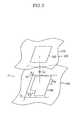
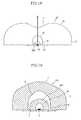
- Fig. 4is a perspective view of an LED according to an embodiment of the present invention.
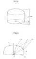
- Fig. 5is a cross-sectional view of the LED of Fig. 4.
- Fig. 6is a reference view for illustrating the refraction of light at the surface of a lens of the LED of Fig. 4.
- an LED 344comprises a light emitting chip 4 and a lens.
- the lensis made of a transparent dielectric material and includes a base 31, a curved circumferential surface 2 which extends from the base 31, and a curved central surface 1 which extends from the curved circumferential surface 2.
- the base 31has a groove for receiving the light emitting chip 4 therein.
- the curved central surface 1 of the lenshas a convex shape when viewed from the light emitting chip 4, and is symmetrical with respect to a lens axis which vertically extends from the center of the light emitting chip 4.
- a distance from a point of the light ray emitting surface of the light emitting chip 4 to a point of the curved central surface 1is always shorter than the radius of curvature for the corresponding point of the curved central surface 1.
- This conditionis hereinafter referred to as "the first condition of the radius of curvature” and results in uniform dispersion of the the light ray emitted from the light emitting chip 4 to a wider area.
- a distance from the center of the base 31 to a point of the curved central surface 1is always shorter than the radius of curvature for the corresponding point of the curved central surface 1.
- This conditionis hereinafter referred to as "the modified first condition of the radius of curvature”.
- it is preferable to construct a lens so that an acute angle formed between a line linking the center of the base 31 to a point of the curved central surface 1 and the main axis of the lensis always larger than an acute angle formed between a normal for the corresponding point of the curved central surface 1 and the main axis of the lens.
- the first condition of light dispersionis hereinafter referred to as "the first condition of light dispersion.
- the shape of the curved circumferential surface 2results by steeply cutting the side of the lens, so that the size of the lens is reduced and incident light which excessively slants toward the side of the lens is redirected to the upper direction of the lens.
- the lensmay be constructed so that the curved circumferential surface 2 satisfies the first condition of the radius of curvature or the first condition of light dispersion. That is, the lens may be constructed in such a way that the curved central surface 1 extends to the base 31, omitting the curved circumferential surface 2.
- the radius of curvatureis more abruptly changed at the boundary area of the curved central surface 1 and the curved circumferential surface 2 as compared with at the curved central surface 1 or at the curved circumferential surface 2, and therefore it may be discontinuous.
- a discontinuous radius of curvaturebrings a discontinuous light distribution. Therefore, it is preferable to trim the boundary corner for a continuous variation of the radius of curvature.
- the position of the boundary of the curved central surface 1 and the curved circumferential surface 2is controlled depending on the light emitting distribution. For example, the boundary of the curved central surface 1 and the curved circumferential surface 2 is placed at an angle between about 20 degrees and about 50 degrees from the center of the groove for receiving the light emitting chip 4.
- the lensis formed in order that the curved central surface 1 covers the light condensed region.
- the light ray emitted from the light emitting chip 4is always refracted in a receding direction from the main axis of the lens. This will be described with reference to Fig. 6.
- the lenssatisfies the first condition of the radius of curvature or the first condition of light dispersion, when the wave plane of the light meets the curved central surface 1 as shown in Fig. 6, the wave plane near the main axis of the lens first enters into the air before passing through the lens. As a result, the incident light is refracted in the receding direction from the main axis of the lens due to the difference of the speed of the light in air and in the lens.
- Fig. 7is a perspective view of an LED according to an embodiment of the present invention
- Fig. 8is a cross-sectional view of the LED of Fig. 7.
- this LEDfurther comprises a central hollow portion upwardly formed from a base 31, and a supporting unit 7 provided on the base 31 for supporting a light emitting chip 4 thereon.
- the central hollow portioncomprises a curved central surface 5 and a curved circumferential surface 6 which are the inner surface of the lens. It is preferable that the curved central surface 5 of the central hollow portion has a convex shape when viewed from the light emitting chip 4 and is symmetrical with respect to the main axis of the lens, which vertically extends from the center of the light emitting chip 4. In this lens, a distance from a point of the light emitting surface of the light emitting chip 4 to a point of the curved central surface 5 is always longer than the radius of curvature for the corresponding point of the curved central surface 5. This condition is hereinafter referred to as "the second condition of the radius of curvature" and results in uniform dispersion of the light ray emitted from the light emitting chip 4 to a wider region.
- a distance from the center of the base 31 to a point of the curved central surface 5 of the central hollow portionis always longer than the radius of curvature for the corresponding point of the curved central surface 5 of the central hollow portion.
- This conditionis hereinafter referred to as "the modified second condition of the radius of curvature”.
- it is preferable to construct the lens so that an acute angle formed between a straight line linking the center of the base 31 to a point of the curved central surface 5 of the central hollow portion and the main axis of the lensis always smaller than an acute angle formed between the normal for the corresponding point of the curved central surface 5 of the central hollow portion and the main axis of the lens.
- This conditionis hereinafter referred to as "the second condition of light dispersion”.
- the supporting unit 7is attached to the base 31 for receiving the light emitting chip 4 therein. It is preferable that the supporting unit 7 is attached to the base 31 so as to not close the bottom opening of the central hollow portion. If the bottom opening were closed, the air in the central hollow portion would expand by the heat generated when the light emitting chip 4 is operating, causing the supporting unit 7 to be separated from the lens.
- the light ray emitted from the light emitting chip 4is always refracted in the receding direction from the main axis of the lens.
- the curved central surface 5 of the central hollow portionshould satisfy the condition of the radius of curvature or the condition of light dispersion opposite to those for the curved central surface 1 of the lens for satisfactory light dispersion.
- Fig. 9is a cross-sectional view of an LED according to an embodiment of the present invention.
- this LEDfurther comprises an uneven pattern 8, which is formed at the curved central surface 1 and the partial curved circumferential surface 2 of the lens.
- the uneven pattern 8can be configured as a minute pattern.
- the uneven pattern 8causes the light ray to disperse more uniformly. It can be formed at the entire curved central surface 1 and the entire curved circumferential surface 2, or only at the boundary of the curved central surface 1 and the curved circumferential surface 2.
- Fig. 10is a cross-sectional view of an LED according to an embodiment of the present invention.
- this LEDfurther comprises an uneven pattern 8 which is formed at the boundary of the curved central surface 1 and the curved circumferential surface 2.
- the uneven pattern 8causes the light ray to disperse more uniformly. It can be formed at the entire curved central surface 1 and the entire curved circumferential surface 2, or only at specific areas of the curved central surface 1 and the curved circumferential surface 2.
- an outline surface resulting by linking top points of the prominences of the uneven pattern 8satisfies the first condition of the radius of curvature or the modified first condition of the radius of curvature or the first condition of light dispersion.
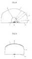
- Fig. 11is a perspective view of an LED according to an embodiment of the present invention
- Fig. 12is a cross-sectional view of the LED of Fig. 11
- Fig. 13is a reference view for illustrating the light reflection at the surface of the lens for the LED of Fig. 11.
- an LEDcomprises a light emitting chip 15 and a lens.
- the lensis formed with a transparent dielectric and includes a base 14, a curved circumferential surface 13 which extends from the base 14, a curved center-edge surface 12 which extends from the curved circumferential surface 13, and a curved centermost surface 11 which extends from the curved center-edge surface 12.
- the base 14has a groove for receiving a light emitting chip 15.
- the curved center-edge surface 12 of the lenshas a convex shape when viewed from the light emitting chip 15, and is symmetrical with respect to the main axis of the lens which vertically extends from the center of the light emitting chip 15.
- a distance from a point of the light emitting surface of the light emitting chip 15 to a point of the curved center-edge surface 12is always shorter than the radius of curvature for the corresponding point of the curved center-edge surface 12 of the lens (i.e., the first condition of the radius of curvature). This is to uniformly disperse the light ray emitted from the light emitting chip 15 to a wider region.
- a distance from the center of the base 14 to a point of the curved center-edge surface 12 of the lensis always shorter than the radius of curvature for the corresponding point of the curved center-edge surface 12 (i.e., the modified first condition of the radius of curvature).
- it is preferable to construct the lens so that an acute angle formed between a straight line linking the center of the base 14 to a point of the curved center-edge surface 12 of the central hollow and the main axis of the lensis always larger than an acute angle formed between the normal for the corresponding point of the curved center-edge surface 12 and the main axis of the lens (i.e., the first condition of light dispersion).
- the curved centermost surface 11 of the lenshas a concave shape when viewed from the light emitting chip 15 and is symmetrical with respect to the main axis of the lens which vertically extends from the center of the light emitting chip 15. Also, the curved centermost surface 11 is formed to satisfy the following equation: A 1 + A 2 ⁇ 90 + sin ⁇ 1 ( 1 / n ) where n is a refraction index, A1 is an obtuse angle formed between the main axis of the lens and a tangent line of a point on the curved centermost surface 11, and A2 is an acute angle formed between a line linking the center of the light emitting chip 15 to the corresponding point of the curved centermost surface 11 and the main axis of the lens.
- the light ray emitted from the light emitting chip 15is refracted at the curved centermost surface 11 and then is dispersed without total internal reflection. In other words, most of the light ray from the light emitting chip 15 is upwardly dispersed passing through the curved centermost surface 11 and the curved center-edge surface 12.
- Equation 1the derivation of Equation 1 will be described with reference to Fig. 13.
- Aiis the angle of incidence measured when the light ray emitted from the light emitting chip 15 is directed toward a point of the curved centermost surface 11
- Aris the angle of refraction
- nis the index of refraction.
- Equation 1means the condition that the total reflection of the light from the light emitting chip 15 does not occur at the curved centermost surface 11.
- the shape of the circumferential curved surface 13results from steeply cutting the side of the lens, so that the size of the lens is reduced and the incident light which excessively slants toward the side of the lens is redirected to the upper direction of the lens.
- the lensmay be constructed so that a distance from a point of the light emitting surface of the light emitting chip 15 to a point of the curved circumferential surface 13 is always shorter than the radius of curvature for the corresponding point of the curved circumferential surface 13 of the lens. That is, the lens may be constructed in such a way that the curved center-edge surface 12 extends until it reaches to the base 14, omitting the formation of the curved circumferential surface 13.
- the radius of curvatureis more abruptly changed at the boundary of the curved centermost surface 11 and the curved center-edge surface 12 and at the boundary of the curved center-edge surface 12 and the curved circumferential surface 13 as compared to at the curved centermost surface 11, the curved center-edge surface 12, or the curved circumferential surface 13.
- the abrupt change in the radius of curvatureresults in a discontinuous radius of curvature, which causes a discontinuous light distribution. Therefore, it is preferable to trim the boundary corners for a continuous variation of the radius of curvature.
- the position of the boundary of the curved centermost surface 11 and the curved center-edge surface 12 and the position of the boundary of the curved center-edge surface 12 and the curved circumferential surface 13are controlled depending on the light emitting distribution.
- the boundary of the curved center-edge surface 12 and the curved circumferential surface 13is positioned at an angle between about 20 degrees and about 50 degrees with respect to the center of the groove. That is, since the light ray emitted from the light emitting chip 15 is condensed within an angle between about 20 degrees and about 50 degrees to the center of the groove and is rarely distributed beyond that range, it is enough that the lens is formed in order that the curved centermost surface 11 and the curved center-edge surface 12 cover the light condensed region.
- the light ray emitted from the light emitting chip 15is always refracted at the curved centermost surface 11 and the curved center-edge surface 12 in the receding direction from the main axis of the lens.
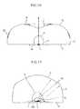
- Fig. 14is a cross-sectional view of a light emitting diode according to an embodiment of the present invention.
- this light emitting diodefurther comprises a central hollow portion upwardly formed from a base 14, and a supporting unit 7 is attached to the base 14 for supporting a light emitting chip 15 thereon.
- the central hollow portioncomprises a curved circumferential surface 17 and a curved central surface 16, which form an inner surface of the lens. It is preferable that the curved central surface 16 of the central hollow portion has a convex shape when viewed from the light emitting chip 15, and is symmetrical with respect to the main axis of the lens which vertically extends from the center of the light emitting chip 15. In this lens, a distance from a point of the light emitting surface of the light emitting chip 15 to a point of the curved central surface 16 of the central hollow portion is always longer than the radius of curvature for the corresponding point of the curved central surface 16 (i.e., the second condition of the radius of curvature). This is to uniformly disperse the light ray emitted from the light emitting chip 15 to a wider region.
- a distance from the center of the base 14 to a point of the curved central surface 16 of the central hollow portionis always longer than the radius of curvature for the corresponding point of the curved central surface 16 (i.e., the modified second condition of the radius of curvature).
- it is preferable to construct the lens so that an acute angle formed between a straight line linking the center of the base 14 to a point of the curved central surface 16 of the central hollow portion and the main axis of the lensis always smaller than an acute angle formed between the normal for the corresponding point of the curved central surface 16 and the main axis of the lens (i.e., the second condition of light dispersion).
- a supporting unit 18is attached to the base 14 for receiving the light emitting chip 15 therein.
- the supporting unit 18is attached to the base 14 not so as to close a bottom opening of the central hollow portion. If the opening were closed, the air in the central hollow portion would expand by the heat generated when the light emitting chip 15 is operating, causing the supporting unit 18 to separate from the lens.
- the central hollow portionis formed to satisfy the above-mentioned conditions, the light ray emitted from the light emitting chip 15 is always refracted at the curved central surface 16 of the central hollow portion in the receding direction from the main axis of the lens.
- Fig. 15is a cross-sectional view of an LED according to an embodiment of the present invention.
- this LEDfurther comprises an uneven pattern 19 which is formed at the entire curved centermost surface 11, the entire curved center-edge surface 12, and the partial curved circumferential surface 13 of the lens.
- the uneven pattern 19as a minute pattern
- the uneven pattern 19causes more uniform dispersion of the light ray and can be formed at the entire curved centermost surface 11, the entire curved center-edge surface 12, and the entire curved circumferential surface 13, or only at the boundary of the second central curved surface 12 and the curved circumferential surface 13.
- Fig. 16is a cross-sectional view of an LED according to an embodiment of the present invention.
- this LEDfurther comprises uneven patterns 19 and 20 which are individually formed at the boundary of the curved centermost surface 11 and the curved center-edge surface 12 and at the boundary of the curved center-edge surface 12 and the circumferential curved surface 13.
- the uneven patterns 19 and 20cause more uniform dispersion of the light ray and can be configured as minute patterns.
- the uneven patterns 19 and 20can be formed entirely over the first central curved surface 11, the second central curved surface 12, and the circumferential curved surface 13, or only at the specific areas of the first central curved surface 11, the second central curved surface 12, and the circumferential curved surface 13.
- an outline surface of the curved center-edge surface 12(created by linking top points of the prominences of the uneven patterns) satisfies the first condition of the radius of curvature or the modified first condition of the radius of curvature or the first condition of light dispersion, and an outline surface of the curved centermost surface 11 satisfies Equation 1.
- Fig. 17is a cross-sectional view of an LED according to an embodiment of the present invention.
- this LEDfurther comprises an inner lens 200 which covers a light emitting chip 4 in a central hollow portion
- the inner lens 200has the same shape as the lens of light emitting diode shown in Fig. 4 and Fig. 5. That is, the inner lens 200 comprises a base, a curved circumferential surface that extends from the base, a curved central surface which extends from the curved circumferential surface, and a groove which is provided in the base for receiving the light emitting chip 4 therein.
- the curved central surface of the inner lens 200satisfies the first condition of the radius of curvature or the first condition of light dispersion.
- the inner lens 200may be formed in such a way that the curved central surface extends to the base, omitting the curved circumferential surface.
- Fig. 18is a cross-sectional view of an LED according to an embodiment of the present invention.
- this LEDfurther comprises an inner lens 200 which covers a light emitting chip 15 in a central hollow portion
- the inner lens 200has the same shape as the lens of light emitting diode shown in Fig. 4 and Fig. 5. That is, the inner lens 200 comprises a base, a curved circumferential surface that extends from the base, a curved central surface which extends from the curved circumferential surface, and a groove which is provided in the base of the inner lens 200 for receiving the light emitting chip 15 therein.
- the curved central surface of the inner lens 200satisfies the first condition of the radius of curvature or the first condition of light dispersion.
- the inner lens 200may be formed in such a way that the curved central surface extends to the base, omitting the curved circumferential surface.
- the inner lenshas the same shape as the lens of the light emitting diode shown in Fig. 4 and Fig. 5, but the shape of the inner lens can be varied.
- the shape of the inner lenscan be varied.
- an LEDincludes an outer lens 101 and an inner lens 401.
- the outer lens 101has the same shape as the lens of the LED of Fig. 7 and Fig. 8.
- the inner lens 401is provided in the central hollow portion of the outer lens 101 and has a central hollow portion 9 therein.
- a light emitting chip 4is provided in the central hollow portion 9 of the inner lens 401.
- the inner lens 401has the same shape as the lens of the LED shown in Fig. 7 and Fig. 8. That is, the inner lens 401 comprises an outer surface, an inner surface defining the central hollow portion 9, and a base.
- the outer surface of the inner lens 401comprises a curved circumferential surface and a curved central surface which satisfies the first condition of the radius of curvature or the first condition of light dispersion, and the inner surface comprises a curved circumferential surface and a curved central surface which satisfies the second condition of the radius of curvature or the second condition of light dispersion.
- an LEDincludes an outer lens 301 and an inner lens 401.
- the outer lens 301has the same shape as the lens of the LED of Fig. 14.
- the inner lens 401is provided in the central hollow portion of the outer lens 301 and has a central hollow portion 9 therein.
- a light emitting chip 15is provided in the central hollow portion 9 of the inner lens 401.
- the inner lens 401has the same shape as the lens of the LED shown in Fig. 7 and Fig. 8. That is, the inner lens 401 comprises an outer surface, an inner surface defining the central hollow portion 9, and a base.
- the outer surface of the inner lens 401comprises a curved circumferential surface and a curved central surface that satisfies the first condition of the radius of curvature or the first condition of light dispersion
- the inner surface of the inner lens 401comprises a curved circumferential surface and a curved central surface that satisfies the second condition of the radius of curvature or the second condition of light dispersion.
- an LEDincludes an outer lens 101 and an inner lens 601.
- the outer lens 101has the same shape as the lens of the LED of Fig. 7 and Fig. 8.
- the inner lens 601is provided in the central hollow portion of the outer lens 101 and covers a light emitting chip 4.
- the inner lens 601has the same shape as the lens of the light emitting diode shown in Fig. 11 and Fig. 12. That is, the inner lens 601 made of a transparent dielectric comprises a base, a curved circumferential surface which extends from the base, a curved center-edge surface which extends from the curved circumferential surface, and a curved centermost surface which extends from the curved center-edge surface.
- a grooveis provided in the base of the inner lens 601 for receiving the light emitting chip 4 therein.
- the curved center-edge surface of the inner lens 601satisfies the first condition of the radius of curvature or the first condition of light dispersion, and the curved centermost surface satisfies Equation 1 relating to the condition that no total refraction is generated.
- an LEDincludes an outer lens 301 and an inner lens 601.
- the outer lens 301has the same shape as the lens of the LED shown in Fig.14.
- the inner lens 601is provided in the central hollow portion of the outer lens 301 and covers a light emitting chip 15.
- the inner lens 601has the same shape as the lens of the LED shown in Fig. 11 and Fig. 12. That is, the inner lens 601 made of a transparent dielectric comprises a base, a curved circumferential surface that extends from the base, a curved center-edge surface that extends from the curved circumferential surface, and a curved centermost surface which extends from the curved center-edge surface.
- a grooveis provided in the base of the inner lens 601 for receiving the light emitting chip 15 therein.
- the curved center-edge surface of the inner lens 601satisfies the first condition of the radius of curvature or the first condition of light dispersion, and the curved centermost surface satisfies Equation 1 relating to the condition that no total refraction is generated.
- an LEDincludes an outer lens 101 and an inner lens 801.
- the outer lens 101has the same shape as the lens of the LED shown in Fig. 7 and Fig. 8.
- the inner lens 801is provided in the central hollow portion of the outer lens 101 and has a central hollow portion 22 therein.
- a light emitting chip 4is provided in the central hollow portion 22 of the inner lens 801.
- the inner lens 801has the same shape as the lens of the LED shown in Fig. 14. That is, the inner lens 801 comprises an outer surface, an inner surface defining the central hollow portion 22, and a base.
- the outer surface of the inner lens 801comprises a curved circumferential surface, a curved center-edge surface which satisfies the first condition of the radius of curvature or the first condition of light dispersion, and a curved centermost surface which satisfies Equation 1 relating to the condition that no total refraction is generated, and the inner surface of the inner lens 801 comprises a curved circumferential surface and a curved central surface which satisfies the second condition of the radius of curvature or the second condition of light dispersion.
- an LEDincludes an outer lens 301 and an inner lens 801.
- the outer lens 301has the same shape as the lens of the LED shown in Fig. 14.
- the inner lens 801is provided in the central hollow portion of the outer lens 301 and has a central hollow portion 22 therein.
- a light emitting chip 15is provided in the central hollow portion 22 of the inner lens 801.
- the inner lens 801has the same shape as the lens of the LED shown in Fig. 14. That is, the inner lens 801 comprises an outer surface, an inner surface defining the central hollow portion 22, and a base.
- the outer surface of the inner lens 801comprises a curved circumferential surface, a curved center-edge surface that satisfies the first condition of the radius of curvature or the first condition of light dispersion, and a curved centermost surface that satisfies Equation 1 relating to the condition that no total refraction is generated.
- the inner surface of the inner lens 801comprises a curved circumferential surface and a curved central surface that satisfies the second condition of the radius of curvature or the second condition of light dispersion.
- the above-mentioned embodiments of the LEDare examples, and more variations can be given.
- the formation of the uneven patterncan be further varied.
- Fig. 25is a graph showing the flux to the incident angle of the light ray from the LEDs according to embodiments of the present invention
- curve C0is the flux to the incident angle of the light ray emitted from the LED shown in Fig. 4 and Fig. 5
- curve C1is the flux to the incident angle of the light ray emitted from the LED shown in Fig. 7 and Fig. 8
- curve C2is the flux to the incident angle of the light ray emitted from the LED shown in Fig. 11 and Fig. 12
- curve C3is the flux to the incident angle of the light ray emitted from the LED shown in Fig. 4 and Fig. 5.
- the fluxis measured at 20mm above the LED.
- the dispersion of the light rayis enlarged in the order of the embodiment shown in Fig. 4 and Fig. 5, the embodiment shown in Fig. 7 and Fig. 8, the embodiment shown in Fig. 11 and Fig. 12, and the embodiment shown in Fig. 14.
- the RGB mixing section for producing the white light and the uniform dispersion section for producing the uniform surface lightcan be minimized.
- an LED according to embodiments of the present inventioncan widen the three-dimensional incident angle, and thus the RGB mixing section for producing the white light and the uniform dispersion section for emitting the uniform surface light can be minimized.
- Such a propertyresults in construction of a compact, slim, and light LCD.
Landscapes
- Physics & Mathematics (AREA)
- Optics & Photonics (AREA)
- General Physics & Mathematics (AREA)
- Nonlinear Science (AREA)
- General Engineering & Computer Science (AREA)
- Engineering & Computer Science (AREA)
- Crystallography & Structural Chemistry (AREA)
- Chemical & Material Sciences (AREA)
- Mathematical Physics (AREA)
- Led Device Packages (AREA)
- Lenses (AREA)
- Planar Illumination Modules (AREA)
- Optical Elements Other Than Lenses (AREA)
- Led Devices (AREA)
- Electroluminescent Light Sources (AREA)
- Liquid Crystal (AREA)
Abstract
Description
- The present disclosure relates to a light source for a display device.
- Display devices used for image display such as in a television receiver or computer monitor are classified into a self-luminescence display and a light-receiving display requiring a separate light source. Light emitting diode (LED), electroluminescence (EL), vacuum fluorescent display (VFD), field emission display (FED), and plasma display panel (PDP) devices, etc., are included in the self-luminescence display device, while liquid crystal displays (LCDs), etc., are included in the light-receiving display devices.
- The LCD includes, for example, a pair of panels individually having electrodes on their inner surfaces, and a dielectric anisotropy liquid crystal layer interposed between the panels. In the LCD, a variation of the voltage difference between the field generating electrodes, i.e., the variation in the strength of an electric field generated by the electrodes, changes the transmittance of the light passing through the LCD, and thus desired images are obtained by controlling the voltage difference between the electrodes.
- In the LCD, a light may be a natural light or an artificial light emitted from a light source unit separately employed in the LCD.
- A backlight device is a representative artificial light source device for the LCD. The backlight device utilizes light emitting diodes (LEDs) or fluorescent lamps such as cold cathode fluorescent lamps (CCFLs), external electrode fluorescent lamps (EEFLs), etc., as the light source.
- The LED is eco-friendly since it does not use mercury (Hg) and it has stable characteristics. For these reasons, the LED is a preferred light source.
- However, some problems may arise when the LED is used as a surface light source device. This is because the light rays emitted from the LED tend to condense to a narrow region.
- According to an embodiment of the present invention, there is provided a lens comprising: a base; a first curved circumferential surface upwardly extending from the base; and a first curved central surface extending from the first curved circumferential surface, wherein a distance from the center of the base to a point of the first curved central surface is shorter than the radius of curvature for the corresponding point of the first curved central surface.
- The lens further comprises a central hollow portion upwardly formed from the base. The central hollow portion is comprised of a second curved circumferential surface and a second curved central surface extending from the second curved circumferential surface, which are inner surfaces of the lens. In this lens, it is preferable that a distance from the center of the base to a point of the second curved central surface is longer than the radius of curvature for the corresponding point of the second curved central surface.
- A boundary region of the second curved central surface and the second curved circumferential surface is preferably placed within about 20 degrees to about 50 degrees with respect to the center of the base Also, a boundary region of the first curved central surface and the first curved circumferential surface is placed within 20 degrees to 50 degrees with respect to the center of the base.
- In this lens, the base includes a groove for receiving a light emitting chip therein, and a distance from the center of the base to a point of the first curved circumferential surface is shorter than the radius of curvature for the corresponding point of the first curved circumferential surface.
- According to another embodiment of the present invention, there is provided a lens which is formed with a material having a refractive index of n, and which comprises: a base; a first curved circumferential surface upwardly extending from the base; a curved center-edge surface extending from the first curved circumferential surface; and a curved centermost surface extending from the curved center-edge surface.
- Here, it is preferable that a distance from a center of the base to a point of the curved center-edge surface is always shorter than the radius of curvature for the corresponding point of the curved center-edge surface.
- The curved centermost surface has a concave shape with respect to the base.
- Here, it is preferable that the lens is constructed to satisfy the following equation:

wherein A1 is an obtuse angle formed between a main axis of the lens and a tangent line of a point of the curved centermost surface, and A2 is an acute angle formed between a straight line linking the center of the base to the corresponding point of the curved centermost surface and the main axis of the lens. - The lens further comprises a central hollow portion upwardly formed from the base of the lens. The central hollow portion includes a second curved circumferential surface and a curved central surface extending from the second curved circumferential surface, which are inner surfaces of the lens.
- Here, it is preferable that a distance from the center of the base to a point of the curved central surface is longer than the radius of curvature for the corresponding point of the curved central surface. When the main axis of the lens is intersected with a tangent line of a boundary point of the curved center-edge surface and the curved centermost surface, they are intersected at an angle of 90 degrees.
- It is also preferable that a boundary region of the curved center-edge surface and the first curved circumferential surface may be placed within about 20 degrees to about 50 degrees with respect to the center of the base The curved centermost surface may be a cone-shaped groove.
- According to another embodiment of the present invention, there is provided an LED comprising: a first lens including a base, a first curved circumferential surface upwardly extending from the base, and a first curved central surface; and a light emitting chip provided under the first lens.
- Here, it is preferable that a distance from a point of an upper surface of the light emitting chip to a point of the first curved central surface is shorter than the radius of curvature for the corresponding point of the first curved central surface.
- The LED further comprises a central hollow portion upwardly formed from the base of the first lens. The central hollow portion includes a second curved circumferential surface and a second curved central surface extending from the second curved circumferential surface, which are inner surfaces of the first lens. Here, it is preferable that a distance from a point of an upper surface of the light emitting chip to a point of the second curved central surface is longer than the radius of curvature for the corresponding point of the second curved central surface.
- The LED further comprises a second lens which is provided in the central hollow portion of the first lens to cover the light emitting chip. The second lens includes a base, a third curved circumferential surface upwardly extending from the base, and a third curved central curved extending from the third curved circumferential surface. In this lens, it is preferable that a distance from a point of an upper surface of the light emitting chip to a point of the third curved central surface is shorter than the radius of curvature for a corresponding point of the third curved central surface.
- The LED further comprises a central hollow portion upwardly formed from the base of the second lens. The central hollow portion includes a fourth curved circumferential surface and a fourth curved central surface extending from the fourth curved circumferential surface, which are inner surfaces of the lens. In the second lens, it is preferable that a distance from a point of an upper surface of the light emitting chip to a point of the fourth curved central surface is longer than the radius of curvature for the corresponding point of the fourth curved central surface.
- The second lens is formed with a material having a refractive index of n, and it includes a base, a fifth curved circumferential surface upwardly extending from the base, a curved center-edge surface extending from the fifth curved circumferential surface, and a curved centermost surface extending from the curved center-edge surface. A groove is formed at the center of the base for receiving the light emitting chip therein.
- In the second lens, it is preferable that a distance from a point of an upper surface of the light emitting chip to a point of the curved center-edge surface is shorter than the radius of curvature for the corresponding point of the curved center-edge surface, and the curved centermost surface has a concave shape when viewed from the light emitting chip.
- The LED further comprises a central hollow portion upwardly formed from the base of the second lens. The central hollow includes a sixth curved circumferential surface and a sixth curved central surface extending from the sixth curved circumferential surface, which are inner surfaces of the second lens. Here, it is preferable that a distance from a point of an upper surface of the light emitting chip to a point of the sixth curved central surface is longer than the radius of curvature for the corresponding point of the sixth curved central surface.
- The LED further comprises a supporting unit which is attached to the base of the first lens for supporting the light emitting chip thereon.
- According to another embodiment of the present invention, there is provided an LED comprised of: a first lens which is formed with a material having a refractive index of n, and the lens includes a base, a first curved circumferential surface upwardly extending from the base, a first curved center-edge surface extending from the first curved circumferential surface, and a first curved centermost surface extending from the first curved center-edge surface; and a light emitting chip which is provided under the first lens.
- In this LED, a distance from a point of an upper surface of the light emitting chip to a point of the first curved center-edge surface is shorter than the radius of curvature for the corresponding point of the first curved center-edge surface. The first curved centermost surface has a concave shape when viewed from the light emitting chip.
- Here, it is preferable that the LED is constructed to satisfy the following equation:

wherein A1 is an obtuse angle formed between the main axis of the first lens and a tangent line of a point of the first curved centermost surface, and A2 is an acute angle formed between a straight line linking the center of the base to the corresponding point of the first curved centermost surface and the main axis of the first lens. - The LED further comprises a central hollow portion upwardly formed from the base of the first lens. The central hollow portion includes a second curved circumferential surface and a first curved central surface extending from the second curved circumferential surface, which are inner surfaces of the first lens. Here, it is preferable that a distance from a point of an upper surface of the light emitting chip to a point of the first curved central surface is longer than the radius of curvature for the corresponding point of the first curved central surface.
- The LED further comprises a second lens which is provided in the central hollow portion of the first lens to cover the light emitting chip. The second lens includes a base, a third curved circumferential surface upwardly extending from the base, and a second curved central surface extending from the third curved circumferential surface.
- Here, it is preferable that a distance from a point of an upper surface of the light emitting chip to a point of the second curved central surface is shorter than the radius of curvature for the corresponding point of the second curved central surface.
- The LED further comprises a central hollow portion upwardly formed from the base of the second lens. The central hollow portion includes a fourth curved circumferential surface and a third curved central surface extending from the fourth curved circumferential surface, which are inner surfaces of the second lens.
- Here, it is also preferable that a distance from a point of an upper surface of the light emitting chip to a point of the third curved central surface is longer than the radius of curvature for the corresponding point of the third curved central surface.
- The second lens is formed with a material having a refractive index of n, and the second lens includes a base, a fifth curved circumferential surface upwardly extending from the base, a second curved center-edge surface extending from the fifth curved circumferential surface, and a second curved centermost surface extending from the second curved center-edge surface.
- Here, it is preferable that a distance from a point of an upper surface of the light emitting chip to a point of the second curved center-edge surface is shorter than the radius of curvature for the corresponding point of the second curved center-edge surface, and the second curved centermost surface has a concave shape when viewed from the light emitting chip.
- The LED further comprises a central hollow portion upwardly formed from the base of the second lens. The central hollow portion is comprised of a sixth curved circumferential surface and a fourth curved central surface extending from the sixth curved circumferential surface, which are inner surfaces of the second lens.
- Here, it is preferable that a distance from a point of an upper surface of the light emitting chip to a point of the fourth curved central surface is longer than the radius of curvature for the corresponding point of the fourth curved central surface.
- The LED further comprises a supporting unit which is attached to the base of the first lens for supporting the light emitting chip thereon.
- In this LED, the first curved centermost surface is a cone-shaped groove.
- According to another embodiment of the present invention, there is provided an LED which comprises: a lens including a base, a first curved circumferential surface upwardly extending from the base, and a first curved central surface; and a light emitting chip provided under the lens.
- In this LED, at least a partial area of the first curved central surface and the first curved circumferential surface includes an uneven pattern. Here, it is preferable that a distance from a point of an upper surface of the light emitting chip to a point of an outline of the first curved central surface is shorter than the radius of curvature for the corresponding point of the outline surface of the first curved central surface.
- The LED further comprises a central hollow portion upwardly formed from the base of the lens. The central hollow portion includes a second curved circumferential surface and a second curved central surface extending from the second curved circumferential surface, which are inner surfaces of the lens. Here, it is preferable that a distance from a point of an upper surface of the light emitting chip to a point of the second curved central surface is longer than the radius of curvature for the corresponding point of the second curved central surface.
- The LED further comprises an inner lens which is provided in the central hollow portion of the lens to cover the light emitting chip. The inner lens includes a base, a curved circumferential surface upwardly extending from the base, and a curved central surface extending from the curved circumferential surface.
- Here, it is preferable that a distance from a point of an upper surface of the light emitting chip to a point of the curved central surface is shorter than the radius of curvature for the corresponding point of the curved central surface.
- In the LED, the uneven pattern is formed at the boundary area of the first curved central surface and the first curved circumferential surface.
- According to another embodiment of the present invention, there is provided an LED which comprises: a lens which is formed with a material having a refractive index of n, and it includes a base, a first curved circumferential surface upwardly extending from the base, a curved central-edge surface extending from the first curved circumferential surface, and a curved centermost surface extending from the curved central-edge surface; and a light emitting chip which is provided under the lens.
- In the LED, at least a partial area of the curved centermost surface, the curved central-edge surface and the first curved circumferential surface includes an uneven pattern. Here, it is preferable that a distance from a point of an upper surface of the light emitting chip to a point of the curved central-edge surface is shorter than the radius of curvature for the corresponding point of an outline surface of the curved central-edge surface, and the curved centermost surface has a concave shape when viewed from the light emitting chip.
- Here, it is preferable that the LED is constructed to satisfy the following equation:

wherein A1 is an obtuse angle formed between the main axis of the lens and a tangent line of a point of the curved centermost surface, and A2 is an acute angle formed between a straight line linking the center of the base to the corresponding point of the curved centermost surface and the main axis of the lens. - The LED further comprises a central hollow portion upwardly formed from the base of the lens. The central hollow portion includes a second curved circumferential surface and a curved central surface upwardly extending from the second curved circumferential surface, which are inner surfaces of the lens.
- Here, it is preferable that a distance from a point of an upper surface of the light emitting chip to a point of the curved central surface is longer than the radius of curvature for the corresponding point of the curved central surface.
- The LED further comprises an inner lens which is provided in the central hollow portion of the lens to cover the light emitting chip. The inner lens includes a base, a curved circumferential surface upwardly extending from the base, and a curved central surface extending from the curved circumferential surface. Here, it is preferable that a distance from a point of an upper surface of the light emitting chip to a point of the curved central surface is shorter than the radius of curvature for the corresponding point of the curved central surface.
- In the LED, the uneven pattern may be formed at the boundary area of the curved centermost surface and the curved center-edge surface and the boundary area of the curved center-edge surface and the first curved circumferential surface. The curved centermost surface may be a cone-shaped groove.
- According to another embodiment of the present invention, there is provided an LED which comprises a lens including a base, a first curved circumferential surface upwardly extending from the base, and a first curved central surface.
- In this LED, an acute angle formed between a straight line linking the center of the base to a point of the first curved central surface and the main axis of the lens is larger than an acute angle formed between the normal for the corresponding point of the first curved surface and the main axis of the lens.
- The LED further comprises a central hollow portion upwardly formed from the base of the lens. The central hollow portion is comprised of a second curved circumferential surface and a second curved central surface extending from the second curved circumferential surface, which are inner surfaces of the lens.
- Here, it is preferable that an acute angle formed between a straight line linking the center of the base to a point of the second curved central surface and the main axis of the lens is smaller than an acute angle formed between the normal for the corresponding point of the second curved central surface and the main axis of the lens.
- According to another embodiment of the present invention, there is provided a lens for an LED, which is formed with a material having a refractive index of n, and is comprised of: a base; a first curved circumferential surface upwardly extending from the base; a curved center-edge surface extending from the first curved circumferential surface; and a curved centermost surface extending from the curved central-edge surface.
- Here, it is preferable that an acute angle formed between a straight line linking the center of the base to a point of the curved center-edge surface and the main axis of the lens is larger than an acute angle formed between the normal for the corresponding point of the curved center-edge surface and the main axis of the lens, and the curved centermost surface has a concave shape when viewed from the base.
- Here, it is preferable that the lens is constructed to satisfy the following equation:

wherein A1 is an obtuse angle formed between the main axis of the lens and a tangent line of a point of the curved centermost surface, and A2 is an acute angle formed between a straight line linking the center of the base to the corresponding point of the curved centermost surface and the main axis of the lens. - The lens further comprises a central hollow portion upwardly formed from the base of the lens. The central hollow portion is comprised of a second curved circumferential surface and a curved central surface extending from the second curved circumferential surface, which are inner surfaces of the lens.
- Here, it is preferable that an acute angle formed between a straight line linking the center of the base to a point of the curved central surface and the main axis of the lens is smaller than an acute angle formed between the normal for the corresponding point of the curved central surface and the main axis of the lens.
- According to another embodiment of the present invention, a lens for a light emitting diode comprises a base, a first curved surface extending from the base, and a second curved surface extending from the first curved surface, wherein a distance from a center of the base to a point of the second curved surface is shorter than a radius of curvature for the point of the first curved central surface.
- The lens may include a hollow portion formed from the base,
wherein the hollow portion is comprised of a third curved surface and a fourth curved surface extending from the third curved surface, and wherein a distance from the center of the base to a point of the fourth curved surface is longer than the radius of curvature for the point of the fourth curved surface. - Preferred embodiments of the present invention can be understood in more detail from the following descriptions taken in conjunction with the accompanying drawings in which:
- Fig. 1 is a block diagram of an LCD according to an embodiment of the present invention.
- Fig. 2 is an exploded perspective view schematically illustrating an LCD according to an embodiment of the present invention
- Fig. 3 is an equivalent circuit view of a pixel unit of an LCD according to an embodiment of the present invention
- Fig. 4 is a perspective view of a light emitting diode according to an embodiment of the present invention.
- Fig. 5 is a cross-sectional view of the light emitting diode of Fig. 4.
- Fig. 6 is a reference view for illustrating the refraction of light at the surface of a lens of the light emitting diode of Fig. 4.
- Fig. 7 is a perspective view of a light emitting diode according to an embodiment of the present invention.
- Fig. 8 is a cross-sectional view of the light emitting diode of Fig. 7.
- Fig. 9 is a cross-sectional view of a light emitting diode according to an embodiment of the present invention.
- Fig. 10 is a cross-sertional view of a light emitting diode according to an embodiment of the present invention.
- Fig. 11 is a perspective view of a light emitting diode according to an embodiment of the present invention.
- Fig. 12 is a cross-sectional view of the light emitting diode of Fig. 11.
- Fig. 13 is a reference view for illustrating the refraction of light at the surface of a lens of the light emitting diode of Fig. 11.
- Fig. 14 through Fig. 18 are cross-sectional views of light emitting diodes according to embodiments of the present invention.
- Fig. 19 through Fig. 24 are cross-sectional views showing LEDs according to embodiments of the present invention.
- Fig. 25 is a graph showing flux to the incident angle of light rays emitted from LEDs according to embodiments of the present invention.
- Preferred embodiments of the present invention will now be described more fully hereinafter with reference to the accompanying drawings, in which preferred embodiments of the invention are shown. The present invention may, however, be embodied in different forms and should not be construed as being limited to the embodiments set forth herein. Rather, these embodiments are provided so that this disclosure will be thorough and complete, and will fully convey the scope of the invention to those skilled in the art.
- In the drawings, the thickness of the layers, films, and regions are exaggerated for clarity. Like numerals refer to like elements throughout. It will be understood that when an element such as a layer, film, region, or substrate is referred to as being "on" another element, it can be directly on the other element or intervening elements may also be present.
- Hereinafter, a light source device for a display device according to preferred embodiments of the present invention will be described in detail with reference to the accompanying drawings.
- Fig. 1 is a block diagram of an LCD according to an embodiment of the present invention, Fig. 2 is an exploded perspective view schematically illustrating an LCD according to an embodiment of the present invention, and Fig. 3 is an equivalent circuit view of pixel unit of an LCD according to an embodiment of the present invention.
- Referring to Fig. 1, an LCD according to an embodiment of the present invention comprises an
LC panel assembly 300, agate driver 400 and adata driver 500 which are connected to theLC panel assembly 300, agray voltage generator 800 connected to thedata driver 400, alight source section 910 for supplying light to theLC panel assembly 300, alight source driver 920 for controlling thelight source section 910, and asignal controller 600 for controlling the above elements. - Referring to Fig. 2, the LCD configuration according to an embodiment of the present invention comprises an
LC module 350 including adisplay unit 330 and aback light 340, afront housing 361 and arear housing 362 for receiving and supporting theLC module 350, and mold frames 363 and 364. - The
display unit 330 includes theLC panel assembly 300, a gate tape carrier package (TCP) 410 and adata TCP 510 which are attached to theLC panel assembly 300, and a gate printed circuit board (PCB) 450 and adata PCB 550 which are individually attached to thecorresponding TCPs - In a structural view shown in Fig. 2 and Fig. 3, the
LC panel assembly 300 includes alower panel 100 and anupper panel 200 facing each other, and an LC layer 3 interposed therebetween. In an equivalent circuit shown in Fig. 1 and Fig. 3, theLC panel assembly 300 includes a plurality of display signal lines G1-Gn and D1-Dm and a plurality of pixels connected thereto and arranged substantially in a matrix. - The display signal lines G1-Gn and D1-Dm are provided on the
lower panel 100 and include a plurality of gate lines G1-Gn for transmitting gate signals (also referred to as "scanning signals"), and a plurality of data lines D1-Dm for transmitting data signals. The gate lines G1-Gn extend substantially in a row direction and substantially parallel to each other, while the data lines D1-Dm extend substantially in a column direction and substantially parallel to each other. - Each pixel includes a switching element Q which are connected to the display signal lines G1-Gn and D1-Dm, and an LC capacitor CLC and a storage capacitor CST which are connected to the switching element Q The storage capacitor CST may be omitted.
- The switching element Q such as a thin film transistor (TFT) is provided on the
lower panel 100 and has three terminals: a control terminal connected to one of the gate lines G1-Gn; an input terminal connected to one of the data lines D1-Dm; and an output terminal connected to both of the LC capacitor CLC and the storage capacitor CST - The LC capacitor CLC includes a
pixel electrode 190 provided on thelower panel 100 and acommon electrode 270 provided on theupper panel 200 as two terminals. The LC layer 3 interposed between the twoelectrodes pixel electrode 190 is connected to the switching element Q, and thecommon electrode 270 is supplied with a common voltage Vcom and covers the entire surface of theupper panel 200. Alternatively, thecommon electrode 270 may be provided on thelower panel 100. At least one of thepixel electrode 190 and thecommon electrode 270 may be shaped as a bar or a stripe. - The storage capacitor CST is an auxiliary capacitor for the LC capacitor CLC. When the
pixel electrode 190 and a separate signal line (not shown) which is provided on thelower panel 100 are overlapped with each other, interposing an insulator therebetween, the overlapped portion becomes the storage capacitor CST. The separate signal line is supplied with a predetermined voltage such as the common voltage Vcom. Alternatively, the storage capacitor CST may be formed by overlapping of the separate signal line with a pixel electrode of the previous gate line which is placed directly before thepixel electrode 190, and interposing an insulator therebetween. - For color display, each pixel uniquely exhibits one of three primary colors (i.e., spatial division), or sequentially exhibits three primary colors in turn depending on time (i.e., temporal division), so that a spatial or temporal sum of the primary colors are recognized as a desired color. Fig. 3 shows an example of the spatial division in which each pixel includes a
color filter 230 for exhibiting one of the primary colors in an area of theupper panel 200 corresponding to thepixel electrode 190. Alternatively, thecolor filter 230 may be provided on or under thepixel electrode 190 of thelower panel 100. - Referring to Fig. 2, the
backlight 340 is mounted under theLC panel assembly 300. Thebacklight 340 comprises a light source unit 349 including a printed circuit board (PCB) 345 and a plurality of light emitting diodes (LEDs) 344 mounted thereon, and alight guiding plate 342 and a plurality ofoptical sheets 343 which are provided between theLC panel assembly 300 and theLEDs 344 for dispersing the light from theLEDs 344 to theLC panel assembly 300. Thebacklight 340 further comprises a reflectingplate 341 which is provided on the PCB 345 for reflecting the light from theLEDs 344 toward theLC panel assembly 300, and includes a plurality of holes where light emitting chips of theLEDs 344 are protruded therethrough. Thebacklight 340 further comprises a mold frame 364 which is provided between the reflectingplate 341 and thelight guiding plate 342 for maintaining a regular interval between the light source unit 349 and thelight guiding plate 342 and for supporting thelight guiding plate 342 and theoptical sheets 343. - The
LEDs 344 as the light source may be white light emitting diodes or a combination of red, green, and blue light emitting diodes. The red light emitting diode, etc. can be used as an auxiliary diode for the white light emitting diode. TheLEDs 344 are arranged on the PCB 345 in a predetermined form, thereby forming the light source unit 349. - Fig. 2 shows three light source units 349, but the number of the light source units 349 can be varied depending on required brightness, screen size of the LCD, etc.
- Polarizers (not shown) are provided on the outer surfaces of the two
panels - Referring to Fig. 1 and Fig. 2, the
gray voltage generator 800 is included in thedata PCB 550 and generates two sets of a plurality of gray voltages related to the transmittance of the pixels. The gray voltages in one set have a positive polarity with respect to the common voltage Vcom, while those of the other set have a negative polarity with respect to the common voltage Vcom. - The
gate drivers 400 are individually mounted on eachgate TCP 410, having the shapes of an integrated circuit (IC) chip, and are individually connected to the gate lines G1-Gn of theLC panel assembly 300 for transmitting the gate signals consisting of combinations of the gate-on voltage Von and the gate―off voltage Voff input from an external device to the gate signal lines G1-Gn. - The
data drivers 500 are individually mounted on eachdata TCP 510, having the shapes of IC chips, and are individually connected to the data lines D1-Dm of theLC panel assembly 300 for transmitting the data voltages which are selected from the gray voltages supplied from thegray voltage generator 800 to the data signal lines D1-Dm. - In another embodiment of the present invention, the
gate driver 400 or thedata driver 500 is directly mounted on thelower panel 100, having the shape of an IC chip, and in still another embodiment of the present invention, thegate driver 400 or thedata driver 500 is integrated into thelower panel 100 along with other elements. In the above cases, thegate PCB 450 or thegate TCP 410 can be omitted. - The
signal controller 600 is included in thedata PCB 550 or thegate PCB 450 for controlling the operation of thegate driver 400 or thedata driver 500. - Hereinafter, the operation of the above-mentioned LCD will be described.
- The
signal controller 600 receives input image signals R, G, and B and input control signals for controlling the display thereof such as a vertical synchronizing signal Vsync, a horizontal synchronizing signal Hsync, a main clock MCLK, a data enable signal DE, etc. from an external graphic controller (not shown). In response to the input image signals R, G, and B and the input control signals, thesignal controller 600 processes the image signals R, G, and B suitably for the operation of theLC panel assembly 300 and generates gate control signals CONT1 and data control signals CONT2, and then outputs the gate control signals CONT1 and the data control signals CONT2 to thegate driver 400 and thedata driver 500, respectively. - The gate control signals CONT1 include a vertical synchronizing start signal STV for indicating the beginning of a frame, a gate clock signal CPV for controlling the output time of the gate-on voltage Von, and an output enable signal OE for defining the duration of the gate-on voltage Von.
- The data control signals CONT2 include a horizontal synchronizing start signal STH for indicating the beginning of data transmission, a load signal LOAD for instructing to apply the data voltages to the data lines D1-Dm, a reverse signal RVS for reversing the polarity of the data voltages with respect to the common voltage Vcom, and a data clock signal HCLK.
- Responsive to the data control signals CONT2 from the
signal controller 600, thedata driver 500 successively receives the image data DAT for a row of the pixels from thesignal controller 600, shifts them, converts the image data DAT into analog data voltages selected from the gray voltages from thegray voltage generator 800, and then applies the data voltages to data lines D1-Dm. - The
gate driver 400 applies the gate-on voltage Von to the gate lines G1-Gn in response to the gate control signals CONT1 from thesignal controller 600, and thereby turns on the switching elements Q connected thereto The data voltages applied to the data lines D1-Dm are applied to the corresponding pixel through the activated switching elements Q. - The difference between the data voltage applied to the pixel and the common voltage Vcom is represented as a voltage across the LC capacitor CLC, namely, a pixel voltage. The LC molecules in the LC capacitor CLC have orientations depending on the magnitude of the pixel voltage.
- The
light source driver 920 controls current applied to thelight source section 910 for switching theLED 344 of thelight source section 910, and also controls the brightness of the light from theLED 344. - When the light emitted from the
LED 344 passes through the LC layer 3, the polarization of the light is varied according to the orientations of the LC molecules. The polarizer converts the difference of the light polarization into a difference of the light transmittance. - By repeating this procedure by a unit of the horizontal period (which is denoted by "1H" and is equal to one period of the horizontal synchronizing signal Hsync, the data enable signal DE, and the gate clock CPV), all gate lines G1-Gn are sequentially supplied with the gate-on voltage Von during a frame, thereby applying the data voltages to all pixels. When the next frame starts after finishing one frame, the reverse control signal RVS applied to the
data driver 500 is controlled such that the polarity of the data voltages is reversed with respect to that of the previous frame (which is referred to as "frame inversion"). The reverse control signal RVS may be also controlled such that the polarity of the data voltages flowing in a data line in one frame are reversed (for example, line inversion and dot inversion), or the polarity of the data voltages in one packet are reversed (for example, column inversion and dot inversion). - Hereinafter, an LED for a backlight device according to an embodiment of the present invention will be described with reference to Fig. 4, Fig. 5, and Fig. 6.
- Fig. 4 is a perspective view of an LED according to an embodiment of the present invention. Fig. 5 is a cross-sectional view of the LED of Fig. 4. Fig. 6 is a reference view for illustrating the refraction of light at the surface of a lens of the LED of Fig. 4.
- Referring to Fig. 4 and Fig. 5, an
LED 344 comprises alight emitting chip 4 and a lens. The lens is made of a transparent dielectric material and includes abase 31, a curvedcircumferential surface 2 which extends from thebase 31, and a curvedcentral surface 1 which extends from the curvedcircumferential surface 2. Thebase 31 has a groove for receiving thelight emitting chip 4 therein. - It is preferable that the curved
central surface 1 of the lens has a convex shape when viewed from thelight emitting chip 4, and is symmetrical with respect to a lens axis which vertically extends from the center of thelight emitting chip 4. In the lens shown in Figs. 4 and 5, a distance from a point of the light ray emitting surface of thelight emitting chip 4 to a point of the curvedcentral surface 1 is always shorter than the radius of curvature for the corresponding point of the curvedcentral surface 1. This condition is hereinafter referred to as "the first condition of the radius of curvature" and results in uniform dispersion of the the light ray emitted from thelight emitting chip 4 to a wider area. - While only considering the lens, it is preferable that a distance from the center of the base 31 to a point of the curved
central surface 1 is always shorter than the radius of curvature for the corresponding point of the curvedcentral surface 1. This condition is hereinafter referred to as "the modified first condition of the radius of curvature". Otherwise, it is preferable to construct a lens so that an acute angle formed between a line linking the center of the base 31 to a point of the curvedcentral surface 1 and the main axis of the lens is always larger than an acute angle formed between a normal for the corresponding point of the curvedcentral surface 1 and the main axis of the lens. This condition is hereinafter referred to as "the first condition of light dispersion". - The shape of the curved
circumferential surface 2 results by steeply cutting the side of the lens, so that the size of the lens is reduced and incident light which excessively slants toward the side of the lens is redirected to the upper direction of the lens. However, if necessary, the lens may be constructed so that the curvedcircumferential surface 2 satisfies the first condition of the radius of curvature or the first condition of light dispersion. That is, the lens may be constructed in such a way that the curvedcentral surface 1 extends to thebase 31, omitting the curvedcircumferential surface 2. - The radius of curvature is more abruptly changed at the boundary area of the curved
central surface 1 and the curvedcircumferential surface 2 as compared with at the curvedcentral surface 1 or at the curvedcircumferential surface 2, and therefore it may be discontinuous. A discontinuous radius of curvature brings a discontinuous light distribution. Therefore, it is preferable to trim the boundary corner for a continuous variation of the radius of curvature. It is also preferable that the position of the boundary of the curvedcentral surface 1 and the curvedcircumferential surface 2 is controlled depending on the light emitting distribution. For example, the boundary of the curvedcentral surface 1 and the curvedcircumferential surface 2 is placed at an angle between about 20 degrees and about 50 degrees from the center of the groove for receiving thelight emitting chip 4. That is, since the light ray emitted from thelight emitting chip 4 is condensed within an angle between about 20 degrees and about 50 degrees from the center of the groove and is rarely distributed beyond that range, it is enough that the lens is formed in order that the curvedcentral surface 1 covers the light condensed region. - In a lens satisfying the first condition of the radius of curvature or the first condition of light dispersion, the light ray emitted from the
light emitting chip 4 is always refracted in a receding direction from the main axis of the lens. This will be described with reference to Fig. 6. - If the lens satisfies the first condition of the radius of curvature or the first condition of light dispersion, when the wave plane of the light meets the curved
central surface 1 as shown in Fig. 6, the wave plane near the main axis of the lens first enters into the air before passing through the lens. As a result, the incident light is refracted in the receding direction from the main axis of the lens due to the difference of the speed of the light in air and in the lens. - Fig. 7 is a perspective view of an LED according to an embodiment of the present invention, and Fig. 8 is a cross-sectional view of the LED of Fig. 7.
- As compared to that of the embodiment described in connection with Figs. 4-6, this LED further comprises a central hollow portion upwardly formed from a
base 31, and a supportingunit 7 provided on thebase 31 for supporting alight emitting chip 4 thereon. - The central hollow portion comprises a curved
central surface 5 and a curvedcircumferential surface 6 which are the inner surface of the lens. It is preferable that the curvedcentral surface 5 of the central hollow portion has a convex shape when viewed from thelight emitting chip 4 and is symmetrical with respect to the main axis of the lens, which vertically extends from the center of thelight emitting chip 4. In this lens, a distance from a point of the light emitting surface of thelight emitting chip 4 to a point of the curvedcentral surface 5 is always longer than the radius of curvature for the corresponding point of the curvedcentral surface 5. This condition is hereinafter referred to as "the second condition of the radius of curvature" and results in uniform dispersion of the light ray emitted from thelight emitting chip 4 to a wider region. - While only considering the lens, it is preferable that a distance from the center of the base 31 to a point of the curved
central surface 5 of the central hollow portion is always longer than the radius of curvature for the corresponding point of the curvedcentral surface 5 of the central hollow portion. This condition is hereinafter referred to as "the modified second condition of the radius of curvature". Otherwise, it is preferable to construct the lens so that an acute angle formed between a straight line linking the center of the base 31 to a point of the curvedcentral surface 5 of the central hollow portion and the main axis of the lens is always smaller than an acute angle formed between the normal for the corresponding point of the curvedcentral surface 5 of the central hollow portion and the main axis of the lens. This condition is hereinafter referred to as "the second condition of light dispersion". - The supporting
unit 7 is attached to thebase 31 for receiving thelight emitting chip 4 therein. It is preferable that the supportingunit 7 is attached to the base 31 so as to not close the bottom opening of the central hollow portion. If the bottom opening were closed, the air in the central hollow portion would expand by the heat generated when thelight emitting chip 4 is operating, causing the supportingunit 7 to be separated from the lens. - When the curved
central surface 5 of the central hollow portion is formed to satisfy the second condition of the radius of curvature or the second condition of light dispersion, the light ray emitted from thelight emitting chip 4 is always refracted in the receding direction from the main axis of the lens. - In accordance with the above, since the light ray emitted from the
light emitting chip 4 enters the lens passing through the air of the central hollow portion, the curvedcentral surface 5 of the central hollow portion should satisfy the condition of the radius of curvature or the condition of light dispersion opposite to those for the curvedcentral surface 1 of the lens for satisfactory light dispersion. - Fig. 9 is a cross-sectional view of an LED according to an embodiment of the present invention.
- As compared to the embodiment shown in Fig. 4 and Fig. 5, this LED further comprises an
uneven pattern 8, which is formed at the curvedcentral surface 1 and the partial curvedcircumferential surface 2 of the lens. Theuneven pattern 8 can be configured as a minute pattern. Theuneven pattern 8 causes the light ray to disperse more uniformly. It can be formed at the entire curvedcentral surface 1 and the entire curvedcircumferential surface 2, or only at the boundary of the curvedcentral surface 1 and the curvedcircumferential surface 2. - Fig. 10 is a cross-sectional view of an LED according to an embodiment of the present invention.
- As compared to that of the embodiment shown in Fig. 7 and Fig. 8, this LED further comprises an
uneven pattern 8 which is formed at the boundary of the curvedcentral surface 1 and the curvedcircumferential surface 2. Theuneven pattern 8 causes the light ray to disperse more uniformly. It can be formed at the entire curvedcentral surface 1 and the entire curvedcircumferential surface 2, or only at specific areas of the curvedcentral surface 1 and the curvedcircumferential surface 2. - In the embodiments shown in Fig. 9 and Fig. 10, although the
uneven pattern 8 is provided at the curvedcentral surface 1 and the curvedcircumferential surface 2, an outline surface resulting by linking top points of the prominences of theuneven pattern 8 satisfies the first condition of the radius of curvature or the modified first condition of the radius of curvature or the first condition of light dispersion. - Fig. 11 is a perspective view of an LED according to an embodiment of the present invention, Fig. 12 is a cross-sectional view of the LED of Fig. 11, and Fig. 13 is a reference view for illustrating the light reflection at the surface of the lens for the LED of Fig. 11.
- Referring to Fig. 11 and Fig. 12, an LED comprises a
light emitting chip 15 and a lens. The lens is formed with a transparent dielectric and includes abase 14, a curvedcircumferential surface 13 which extends from thebase 14, a curved center-edge surface 12 which extends from the curvedcircumferential surface 13, and a curvedcentermost surface 11 which extends from the curved center-edge surface 12. Thebase 14 has a groove for receiving alight emitting chip 15. - It is preferable that the curved center-
edge surface 12 of the lens has a convex shape when viewed from thelight emitting chip 15, and is symmetrical with respect to the main axis of the lens which vertically extends from the center of thelight emitting chip 15. In this lens, a distance from a point of the light emitting surface of thelight emitting chip 15 to a point of the curved center-edge surface 12 is always shorter than the radius of curvature for the corresponding point of the curved center-edge surface 12 of the lens (i.e., the first condition of the radius of curvature). This is to uniformly disperse the light ray emitted from thelight emitting chip 15 to a wider region. - While only considering the lens, it is preferable that a distance from the center of the base 14 to a point of the curved center-
edge surface 12 of the lens is always shorter than the radius of curvature for the corresponding point of the curved center-edge surface 12 (i.e., the modified first condition of the radius of curvature). Otherwise, it is preferable to construct the lens so that an acute angle formed between a straight line linking the center of the base 14 to a point of the curved center-edge surface 12 of the central hollow and the main axis of the lens is always larger than an acute angle formed between the normal for the corresponding point of the curved center-edge surface 12 and the main axis of the lens (i.e., the first condition of light dispersion). - It is preferable that the curved
centermost surface 11 of the lens has a concave shape when viewed from thelight emitting chip 15 and is symmetrical with respect to the main axis of the lens which vertically extends from the center of thelight emitting chip 15. Also, the curvedcentermost surface 11 is formed to satisfy the following equation:
where n is a refraction index, A1 is an obtuse angle formed between the main axis of the lens and a tangent line of a point on the curvedcentermost surface 11, and A2 is an acute angle formed between a line linking the center of thelight emitting chip 15 to the corresponding point of the curvedcentermost surface 11 and the main axis of the lens. - When the curved
centermost surface 11 satisfies the above equation, the light ray emitted from thelight emitting chip 15 is refracted at the curvedcentermost surface 11 and then is dispersed without total internal reflection. In other words, most of the light ray from thelight emitting chip 15 is upwardly dispersed passing through the curvedcentermost surface 11 and the curved center-edge surface 12. - In this manner, since most of the light ray is directly dispersed upward without the reflection, the light ray from the light emitting diode can be efficiently used.
- Hereinafter, the derivation of
Equation 1 will be described with reference to Fig. 13. - In Fig. 13,Ai is the angle of incidence measured when the light ray emitted from the
light emitting chip 15 is directed toward a point of the curvedcentermost surface 11,Ar is the angle of refraction, andn is the index of refraction. With these elements, Snell's Law is expressed by the following equation:
- If a total internal reflection occurs,Ar is 90 degrees. Accordingly, the critical angle of incidenceAi is derived by the following equations:


- Therefore, the condition that the total internal reflection does not occur is expressed by the following equation:

- In Fig. 13, since the sum of the internal angles of a triangle is 180 degrees, the following equation is given:

- In Fig. 13, the following equation is also given:

- From the
equations Equation 1 is derived That is,Equation 1 means the condition that the total reflection of the light from thelight emitting chip 15 does not occur at the curvedcentermost surface 11. - The shape of the circumferential
curved surface 13 results from steeply cutting the side of the lens, so that the size of the lens is reduced and the incident light which excessively slants toward the side of the lens is redirected to the upper direction of the lens. If necessary, the lens may be constructed so that a distance from a point of the light emitting surface of thelight emitting chip 15 to a point of the curvedcircumferential surface 13 is always shorter than the radius of curvature for the corresponding point of the curvedcircumferential surface 13 of the lens. That is, the lens may be constructed in such a way that the curved center-edge surface 12 extends until it reaches to thebase 14, omitting the formation of the curvedcircumferential surface 13. - The radius of curvature is more abruptly changed at the boundary of the curved
centermost surface 11 and the curved center-edge surface 12 and at the boundary of the curved center-edge surface 12 and the curvedcircumferential surface 13 as compared to at the curvedcentermost surface 11, the curved center-edge surface 12, or the curvedcircumferential surface 13. The abrupt change in the radius of curvature results in a discontinuous radius of curvature, which causes a discontinuous light distribution. Therefore, it is preferable to trim the boundary corners for a continuous variation of the radius of curvature. - It is also preferable that the position of the boundary of the curved
centermost surface 11 and the curved center-edge surface 12 and the position of the boundary of the curved center-edge surface 12 and the curvedcircumferential surface 13 are controlled depending on the light emitting distribution. For example, the boundary of the curved center-edge surface 12 and the curvedcircumferential surface 13 is positioned at an angle between about 20 degrees and about 50 degrees with respect to the center of the groove. That is, since the light ray emitted from thelight emitting chip 15 is condensed within an angle between about 20 degrees and about 50 degrees to the center of the groove and is rarely distributed beyond that range, it is enough that the lens is formed in order that the curvedcentermost surface 11 and the curved center-edge surface 12 cover the light condensed region. - When the first curved
centermost surface 11 satisfiesEquation 1 and the curved center-edge surface 12 satisfies the first condition of the radius of curvature, the light ray emitted from thelight emitting chip 15 is always refracted at the curvedcentermost surface 11 and the curved center-edge surface 12 in the receding direction from the main axis of the lens. - Fig. 14 is a cross-sectional view of a light emitting diode according to an embodiment of the present invention.
- As compared to that of the embodiment shown in Fig. 11 and Fig. 12, this light emitting diode further comprises a central hollow portion upwardly formed from a
base 14, and a supportingunit 7 is attached to thebase 14 for supporting alight emitting chip 15 thereon. - The central hollow portion comprises a curved
circumferential surface 17 and a curvedcentral surface 16, which form an inner surface of the lens. It is preferable that the curvedcentral surface 16 of the central hollow portion has a convex shape when viewed from thelight emitting chip 15, and is symmetrical with respect to the main axis of the lens which vertically extends from the center of thelight emitting chip 15. In this lens, a distance from a point of the light emitting surface of thelight emitting chip 15 to a point of the curvedcentral surface 16 of the central hollow portion is always longer than the radius of curvature for the corresponding point of the curved central surface 16 (i.e., the second condition of the radius of curvature). This is to uniformly disperse the light ray emitted from thelight emitting chip 15 to a wider region. - While only considering the lens, it is preferable that a distance from the center of the base 14 to a point of the curved
central surface 16 of the central hollow portion is always longer than the radius of curvature for the corresponding point of the curved central surface 16 (i.e., the modified second condition of the radius of curvature). Otherwise, it is preferable to construct the lens so that an acute angle formed between a straight line linking the center of the base 14 to a point of the curvedcentral surface 16 of the central hollow portion and the main axis of the lens is always smaller than an acute angle formed between the normal for the corresponding point of the curvedcentral surface 16 and the main axis of the lens (i.e., the second condition of light dispersion). - A supporting
unit 18 is attached to thebase 14 for receiving thelight emitting chip 15 therein. Here, it is preferable that the supportingunit 18 is attached to the base 14 not so as to close a bottom opening of the central hollow portion. If the opening were closed, the air in the central hollow portion would expand by the heat generated when thelight emitting chip 15 is operating, causing the supportingunit 18 to separate from the lens. - If the central hollow portion is formed to satisfy the above-mentioned conditions, the light ray emitted from the
light emitting chip 15 is always refracted at the curvedcentral surface 16 of the central hollow portion in the receding direction from the main axis of the lens. - Fig. 15 is a cross-sectional view of an LED according to an embodiment of the present invention.
- As compared to that of the embodiment shown in Fig. 11 and Fig. 12, this LED further comprises an
uneven pattern 19 which is formed at the entire curvedcentermost surface 11, the entire curved center-edge surface 12, and the partial curvedcircumferential surface 13 of the lens. Theuneven pattern 19 as a minute pattern Theuneven pattern 19 causes more uniform dispersion of the light ray and can be formed at the entire curvedcentermost surface 11, the entire curved center-edge surface 12, and the entire curvedcircumferential surface 13, or only at the boundary of the second centralcurved surface 12 and the curvedcircumferential surface 13. - Fig. 16 is a cross-sectional view of an LED according to an embodiment of the present invention.
- As compared to that of the embodiment shown in Fig. 14, this LED further comprises
uneven patterns centermost surface 11 and the curved center-edge surface 12 and at the boundary of the curved center-edge surface 12 and the circumferentialcurved surface 13. Theuneven patterns uneven patterns curved surface 11, the second centralcurved surface 12, and the circumferentialcurved surface 13, or only at the specific areas of the first centralcurved surface 11, the second centralcurved surface 12, and the circumferentialcurved surface 13. - In the embodiments shown in Fig. 15 and Fig. 16, although the
uneven patterns centermost surface 11, the curved center-edge surface 12, and the curvedcircumferential surface 13, an outline surface of the curved center-edge surface 12 (created by linking top points of the prominences of the uneven patterns) satisfies the first condition of the radius of curvature or the modified first condition of the radius of curvature or the first condition of light dispersion, and an outline surface of the curvedcentermost surface 11 satisfiesEquation 1. - Fig. 17 is a cross-sectional view of an LED according to an embodiment of the present invention.
- As compared to that of the embodiment shown in Fig. 7 and Fig. 8, this LED further comprises an
inner lens 200 which covers alight emitting chip 4 in a central hollow portion Theinner lens 200 has the same shape as the lens of light emitting diode shown in Fig. 4 and Fig. 5. That is, theinner lens 200 comprises a base, a curved circumferential surface that extends from the base, a curved central surface which extends from the curved circumferential surface, and a groove which is provided in the base for receiving thelight emitting chip 4 therein. The curved central surface of theinner lens 200 satisfies the first condition of the radius of curvature or the first condition of light dispersion. Also, theinner lens 200 may be formed in such a way that the curved central surface extends to the base, omitting the curved circumferential surface. - In the LED shown in Fig. 17, since the refraction is generated at the outer surface of the inner lens, the inner surface of outer lens, and the outer surface of the outer lens, the light ray is dispersed to a wider region.
- Fig. 18 is a cross-sectional view of an LED according to an embodiment of the present invention.
- As compared to that of the embodiment shown in Fig. 14, this LED further comprises an
inner lens 200 which covers alight emitting chip 15 in a central hollow portion Theinner lens 200 has the same shape as the lens of light emitting diode shown in Fig. 4 and Fig. 5. That is, theinner lens 200 comprises a base, a curved circumferential surface that extends from the base, a curved central surface which extends from the curved circumferential surface, and a groove which is provided in the base of theinner lens 200 for receiving thelight emitting chip 15 therein. The curved central surface of theinner lens 200 satisfies the first condition of the radius of curvature or the first condition of light dispersion. Also, theinner lens 200 may be formed in such a way that the curved central surface extends to the base, omitting the curved circumferential surface. - In the LED shown in Fig. 18, since the refraction is generated at the outer surface of the inner lens, the inner surface of the outer lens, and the outer surface of the outer lens, the light ray is dispersed to a wider region.
- In the embodiments shown in Fig. 17 and Fig. 18, the inner lens has the same shape as the lens of the light emitting diode shown in Fig. 4 and Fig. 5, but the shape of the inner lens can be varied. Hereinafter, such variations will be described
- Referring to Fig. 19, an LED includes an
outer lens 101 and aninner lens 401. Theouter lens 101 has the same shape as the lens of the LED of Fig. 7 and Fig. 8. Theinner lens 401 is provided in the central hollow portion of theouter lens 101 and has a centralhollow portion 9 therein. Alight emitting chip 4 is provided in the centralhollow portion 9 of theinner lens 401. Theinner lens 401 has the same shape as the lens of the LED shown in Fig. 7 and Fig. 8. That is, theinner lens 401 comprises an outer surface, an inner surface defining the centralhollow portion 9, and a base. The outer surface of theinner lens 401 comprises a curved circumferential surface and a curved central surface which satisfies the first condition of the radius of curvature or the first condition of light dispersion, and the inner surface comprises a curved circumferential surface and a curved central surface which satisfies the second condition of the radius of curvature or the second condition of light dispersion. - In the LED shown in Fig. 19, since the refraction is generated at the inner and outer surfaces of the inner lens, and at the inner and outer surfaces of the outer lens, the light ray is dispersed to a wider region.
- Referring to Fig. 20, an LED includes an
outer lens 301 and aninner lens 401. Theouter lens 301 has the same shape as the lens of the LED of Fig. 14. Theinner lens 401 is provided in the central hollow portion of theouter lens 301 and has a centralhollow portion 9 therein. Alight emitting chip 15 is provided in the centralhollow portion 9 of theinner lens 401. Theinner lens 401 has the same shape as the lens of the LED shown in Fig. 7 and Fig. 8. That is, theinner lens 401 comprises an outer surface, an inner surface defining the centralhollow portion 9, and a base. The outer surface of theinner lens 401 comprises a curved circumferential surface and a curved central surface that satisfies the first condition of the radius of curvature or the first condition of light dispersion The inner surface of theinner lens 401 comprises a curved circumferential surface and a curved central surface that satisfies the second condition of the radius of curvature or the second condition of light dispersion. - In the LED shown in Fig. 20, since the refraction is generated at the inner and outer surfaces of the inner lens, and at the inner and outer surfaces of outer lens, the light ray is dispersed to a wider region.
- Referring to Fig. 21, an LED includes an
outer lens 101 and aninner lens 601. Theouter lens 101 has the same shape as the lens of the LED of Fig. 7 and Fig. 8. Theinner lens 601 is provided in the central hollow portion of theouter lens 101 and covers alight emitting chip 4. Theinner lens 601 has the same shape as the lens of the light emitting diode shown in Fig. 11 and Fig. 12. That is, theinner lens 601 made of a transparent dielectric comprises a base, a curved circumferential surface which extends from the base, a curved center-edge surface which extends from the curved circumferential surface, and a curved centermost surface which extends from the curved center-edge surface. A groove is provided in the base of theinner lens 601 for receiving thelight emitting chip 4 therein. The curved center-edge surface of theinner lens 601 satisfies the first condition of the radius of curvature or the first condition of light dispersion, and the curved centermost surface satisfiesEquation 1 relating to the condition that no total refraction is generated. - In the LED shown in Fig. 21, since the refraction is generated at the outer surface of the inner lens, and at the inner and outer surfaces of the outer lens, the light ray is dispersed to a wider region.
- Referring to Fig. 22, an LED includes an
outer lens 301 and aninner lens 601. Theouter lens 301 has the same shape as the lens of the LED shown in Fig.14. Theinner lens 601 is provided in the central hollow portion of theouter lens 301 and covers alight emitting chip 15. Theinner lens 601 has the same shape as the lens of the LED shown in Fig. 11 and Fig. 12. That is, theinner lens 601 made of a transparent dielectric comprises a base, a curved circumferential surface that extends from the base, a curved center-edge surface that extends from the curved circumferential surface, and a curved centermost surface which extends from the curved center-edge surface. A groove is provided in the base of theinner lens 601 for receiving thelight emitting chip 15 therein. The curved center-edge surface of theinner lens 601 satisfies the first condition of the radius of curvature or the first condition of light dispersion, and the curved centermost surface satisfiesEquation 1 relating to the condition that no total refraction is generated. - In the LED shown in Fig. 22, since the refraction is generated at the outer surface of the inner lens, and at the inner and outer surfaces of outer lens, the light ray is dispersed to a wider region.
- Referring to Fig. 23, an LED includes an
outer lens 101 and aninner lens 801. Theouter lens 101 has the same shape as the lens of the LED shown in Fig. 7 and Fig. 8. Theinner lens 801 is provided in the central hollow portion of theouter lens 101 and has a centralhollow portion 22 therein. Alight emitting chip 4 is provided in the centralhollow portion 22 of theinner lens 801. Theinner lens 801 has the same shape as the lens of the LED shown in Fig. 14. That is, theinner lens 801 comprises an outer surface, an inner surface defining the centralhollow portion 22, and a base. The outer surface of theinner lens 801 comprises a curved circumferential surface, a curved center-edge surface which satisfies the first condition of the radius of curvature or the first condition of light dispersion, and a curved centermost surface which satisfiesEquation 1 relating to the condition that no total refraction is generated, and the inner surface of theinner lens 801 comprises a curved circumferential surface and a curved central surface which satisfies the second condition of the radius of curvature or the second condition of light dispersion. - In the LED shown in Fig. 23, since the refraction is generated at the inner and outer surfaces of the inner lens, and at the inner and outer surfaces of the outer lens, the light ray is dispersed to a wider region.
- Referring to Fig. 24, an LED includes an
outer lens 301 and aninner lens 801. Theouter lens 301 has the same shape as the lens of the LED shown in Fig. 14. Theinner lens 801 is provided in the central hollow portion of theouter lens 301 and has a centralhollow portion 22 therein. Alight emitting chip 15 is provided in the centralhollow portion 22 of theinner lens 801. Theinner lens 801 has the same shape as the lens of the LED shown in Fig. 14. That is, theinner lens 801 comprises an outer surface, an inner surface defining the centralhollow portion 22, and a base. The outer surface of theinner lens 801 comprises a curved circumferential surface, a curved center-edge surface that satisfies the first condition of the radius of curvature or the first condition of light dispersion, and a curved centermost surface that satisfiesEquation 1 relating to the condition that no total refraction is generated. The inner surface of theinner lens 801 comprises a curved circumferential surface and a curved central surface that satisfies the second condition of the radius of curvature or the second condition of light dispersion. - In the LED shown in Fig. 24, since the refraction is generated at the inner and outer surfaces of the inner lens, and at the inner and outer surfaces of the outer lens, the light ray is dispersed to a wider region.
- The above-mentioned embodiments of the LED are examples, and more variations can be given. For example, the formation of the uneven pattern can be further varied.
- Fig. 25 is a graph showing the flux to the incident angle of the light ray from the LEDs according to embodiments of the present invention
- In Fig. 25, curve C0 is the flux to the incident angle of the light ray emitted from the LED shown in Fig. 4 and Fig. 5, curve C1 is the flux to the incident angle of the light ray emitted from the LED shown in Fig. 7 and Fig. 8, curve C2 is the flux to the incident angle of the light ray emitted from the LED shown in Fig. 11 and Fig. 12, and curve C3 is the flux to the incident angle of the light ray emitted from the LED shown in Fig. 4 and Fig. 5. The flux is measured at 20mm above the LED.
- As shown in Fig. 25, the dispersion of the light ray is enlarged in the order of the embodiment shown in Fig. 4 and Fig. 5, the embodiment shown in Fig. 7 and Fig. 8, the embodiment shown in Fig. 11 and Fig. 12, and the embodiment shown in Fig. 14.
- As the incident angle of the light ray emitted from the LED increases, the RGB mixing section for producing the white light and the uniform dispersion section for producing the uniform surface light can be minimized.
- Accordingly, an LED according to embodiments of the present invention can widen the three-dimensional incident angle, and thus the RGB mixing section for producing the white light and the uniform dispersion section for emitting the uniform surface light can be minimized. Such a property results in construction of a compact, slim, and light LCD.
- Although the illustrative embodiments have been described herein with reference to the accompanying drawings, it is to be understood that the present invention is not limited to those precise embodiments, and that various other changes and modifications may be affected therein by one of ordinary skill in the related art without departing from the scope or spirit of the invention. All such changes and modifications are intended to be included within the scope of the invention as defined by the appended claims.
- Where technical features mentioned in any claim are followed by reference signs, those reference signs have been included for the sole purpose of increasing the intelligibility of the claims and accordingly such reference signs do not have any limiting effect on the scope of each element identified by way of example by such reference signs.


Claims (16)
- A lens for a light emitting diode, comprising:a base;a first curved circumferential surface extending from the base; anda first curved central surface extending from the first curved circumferential surface,wherein a distance from a center of the base to a point of the first curved central surface is shorter than a radius of curvature for the point of the first curved central surface.
- The lens of claim 1, wherein the lens includes a hollow portion formed from the base,
wherein the hollow portion forms an inner surface of the lens and is comprised of a second curved circumferential surface and a second curved central surface extending from the second curved circumferential surface, and
wherein a distance from the center of the base to a point of the second curved central surface is longer than a radius of curvature for the point of the second curved central surface. - The lens of claim 2, wherein a boundary region of the second curved central surface and the second curved circumferential surface is placed within about 20 degrees to about 50 degrees with respect to the center of the base.
- The lens of claim 1, wherein a boundary region of the first curved central surface and the first curved circumferential surface is placed within about 20 degrees to about 50 degrees with respect to the center of the base.
- The lens of claim 1, wherein the base includes a groove for receiving a light emitting chip, and
wherein a distance from the center of the base to a point of the first curved circumferential surface is shorter than a radius of curvature for the point of the first curved circumferential surface. - A lens for a light emitting diode formed from a material having a refractive index of n, the lens comprising:a base;a first curved circumferential surface extending from the base;a curved center-edge surface extending from the first curved circumferential surface, anda curved centermost surface extending from the curved center-edge surface,wherein a distance from a center of the base to a point of the curved center-edge surface is shorter than a radius of curvature for the point of the curved center-edge surface, and
wherein the curved centermost surface has a concave shape when viewed from the center of the base. - The lens of claim 6, wherein, when A1 is an obtuse angle formed between a main axis of the lens and a tangent line of a point on the curved centermost surface, and A2 is an acute angle formed between a straight line linking the center of the base to the point on the curved centermost surface and the main axis of the lens, A1+A2 < 90+sin-1(1/n).
- The lens of claim 6, wherein the lens includes a hollow portion formed from the base of the lens,
wherein the hollow portion forms an inner surface of the lens and is comprised of a second curved circumferential surface and a curved central surface extending from the second curved circumferential surface, and
wherein a distance from the center of the base to a point of the curved central surface is longer than a radius of curvature for the point of the curved central surface. - The lens of claim 6, wherein a main axis of the lens is intersected with a tangent line of a boundary point of the curved center-edge surface and the curved centermost surface at an angle of 90 degrees.
- The lens of claim 6, wherein a boundary region of the curved center-edge surface and the first curved circumferential surface is positioned within about 20 degrees to about 50 degrees with respect to a center axis of the base.
- The lens of claim 6, wherein the curved centermost surface forms a cone-shaped groove.
- A lens for a light emitting diode formed from a material having a refractive index of n, the lens comprising:a base;a first curved circumferential surface extending from the base;a curved center-edge surface extending from the first curved circumferential surface; anda curved centermost surface extending from the curved central-edge surface,wherein an acute angle formed between a straight line linking a center of the base to a point of the curved center-edge surface and a main axis of the lens is larger than an acute angle formed between the normal for the point of the curved center-edge surface and the main axis of the lens, and
wherein the curved centermost surface has a concave shape when viewed from the center of the base. - The lens of claim 12, wherein, when A1 is an obtuse angle formed between the main axis of the lens and a tangent line of a point on the curved centermost surface, and A2 is an acute angle formed between a straight line linking the center of the base to the point of the curved centermost surface and the main axis of the lens, A1+A2 < 90+sin-1(1/n).
- The lens of claim 12, wherein the lens includes a hollow portion formed from the base of the lens,
wherein the hollow portion forms an inner surface of the lens and is comprised of a second curved circumferential surface and a curved central surface extending from the second curved circumferential surface,
wherein an acute angle formed between a straight line linking the center of the base to a point of the curved central surface and the main axis of the lens is smaller than an acute angle formed between the normal for the point of the curved central surface and the main axis of the lens. - A lens for a light emitting diode, comprising:a base;a first curved surface extending from the base; anda second curved surface extending from the first curved surface,wherein a distance from a center of the base to a point of the second curved surface is shorter than a radius of curvature for the point of the first curved central surface.
- The lens of claim 15, wherein the lens includes a hollow portion formed from the base,
wherein the hollow portion is comprised of a third curved surface and a fourth curved surface extending from the third curved surface, andwherein a distance from the center of the base to a point of the fourth curved surface is longer than the radius of curvature for the point of the fourth curved surface.
Applications Claiming Priority (1)
| Application Number | Priority Date | Filing Date | Title |
|---|---|---|---|
| KR1020040083146AKR101080355B1 (en) | 2004-10-18 | 2004-10-18 | Light emitting diode, lens for the same |
Publications (3)
| Publication Number | Publication Date |
|---|---|
| EP1653254A2true EP1653254A2 (en) | 2006-05-03 |
| EP1653254A3 EP1653254A3 (en) | 2006-06-07 |
| EP1653254B1 EP1653254B1 (en) | 2024-07-24 |
Family
ID=35892646
Family Applications (1)
| Application Number | Title | Priority Date | Filing Date |
|---|---|---|---|
| EP05107875.6AExpired - LifetimeEP1653254B1 (en) | 2004-10-18 | 2005-08-29 | Light emitting diode and lens for the same |
Country Status (6)
| Country | Link |
|---|---|
| US (4) | US7572036B2 (en) |
| EP (1) | EP1653254B1 (en) |
| JP (4) | JP5264043B2 (en) |
| KR (1) | KR101080355B1 (en) |
| CN (1) | CN100465723C (en) |
| TW (3) | TWI596382B (en) |
Cited By (43)
| Publication number | Priority date | Publication date | Assignee | Title |
|---|---|---|---|---|
| WO2007036186A1 (en)* | 2005-09-30 | 2007-04-05 | Osram Opto Semiconductors Gmbh | Illumination arrangement |
| EP1860467A1 (en)* | 2006-05-24 | 2007-11-28 | Industrial Technology Research Institute | Lens and light emitting diode using the lens to achieve homogeneous illumination |
| WO2008014771A1 (en)* | 2006-07-31 | 2008-02-07 | Osram Opto Semiconductors Gmbh | Lighting assembly |
| EP2015126A1 (en)* | 2007-07-10 | 2009-01-14 | C.R.F. Società Consortile per Azioni | Light emitting diode with a beam shaping device for backlighting a dashboard |
| US7582913B2 (en) | 2004-12-29 | 2009-09-01 | Industrial Technology Research Institute | Lens and LED using the lens to achieve homogeneous illumination |
| WO2009039824A3 (en)* | 2007-09-28 | 2009-10-15 | Osram Opto Semiconductors Gmbh | Optoelectronic component and decoupling lens for an optoelectronic component |
| WO2009147070A1 (en)* | 2008-06-03 | 2009-12-10 | Siemens Aktiengesellschaft | Lighting system |
| EP2378338A1 (en)* | 2010-04-07 | 2011-10-19 | Enplas Corporation | Light flux controlling member, light emitting device, and lighting device |
| EP2461381A3 (en)* | 2004-09-27 | 2013-08-07 | Enplas Corporation | Emission device with light source and light flux control member |
| WO2014011469A1 (en)* | 2012-07-09 | 2014-01-16 | Cree, Inc. | Light emitting diode primary optic for beam shaping |
| US8735920B2 (en) | 2006-07-31 | 2014-05-27 | Cree, Inc. | Light emitting diode package with optical element |
| US8748915B2 (en) | 2006-04-24 | 2014-06-10 | Cree Hong Kong Limited | Emitter package with angled or vertical LED |
| WO2014093245A1 (en)* | 2012-12-12 | 2014-06-19 | Cree, Inc. | Light emitting diode with an improved color spatial uniformity |
| US8791471B2 (en) | 2008-11-07 | 2014-07-29 | Cree Hong Kong Limited | Multi-chip light emitting diode modules |
| US8866169B2 (en) | 2007-10-31 | 2014-10-21 | Cree, Inc. | LED package with increased feature sizes |
| US8905575B2 (en) | 2012-02-09 | 2014-12-09 | Cree, Inc. | Troffer-style lighting fixture with specular reflector |
| TWI480596B (en)* | 2013-12-19 | 2015-04-11 | Lextar Electronics Corp | Light-emitting module and optical lens thereof |
| US9035439B2 (en) | 2006-03-28 | 2015-05-19 | Cree Huizhou Solid State Lighting Company Limited | Apparatus, system and method for use in mounting electronic elements |
| US9070850B2 (en) | 2007-10-31 | 2015-06-30 | Cree, Inc. | Light emitting diode package and method for fabricating same |
| US9200777B2 (en) | 2010-12-01 | 2015-12-01 | Nalux Co., Ltd. | Optical element and illumination device using the same |
| EP2993508A1 (en)* | 2014-08-28 | 2016-03-09 | Hon Hai Precision Industry Co., Ltd. | Lens, light emitting device and backlight module |
| US9423104B2 (en) | 2013-03-14 | 2016-08-23 | Cree, Inc. | Linear solid state lighting fixture with asymmetric light distribution |
| US9494304B2 (en) | 2012-11-08 | 2016-11-15 | Cree, Inc. | Recessed light fixture retrofit kit |
| US9601670B2 (en) | 2014-07-11 | 2017-03-21 | Cree, Inc. | Method to form primary optic with variable shapes and/or geometries without a substrate |
| US9711703B2 (en) | 2007-02-12 | 2017-07-18 | Cree Huizhou Opto Limited | Apparatus, system and method for use in mounting electronic elements |
| US9722158B2 (en) | 2009-01-14 | 2017-08-01 | Cree Huizhou Solid State Lighting Company Limited | Aligned multiple emitter package |
| US9777897B2 (en) | 2012-02-07 | 2017-10-03 | Cree, Inc. | Multiple panel troffer-style fixture |
| US9822951B2 (en) | 2010-12-06 | 2017-11-21 | Cree, Inc. | LED retrofit lens for fluorescent tube |
| US9874322B2 (en) | 2012-04-10 | 2018-01-23 | Cree, Inc. | Lensed troffer-style light fixture |
| US10012354B2 (en) | 2015-06-26 | 2018-07-03 | Cree, Inc. | Adjustable retrofit LED troffer |
| US10054274B2 (en) | 2012-03-23 | 2018-08-21 | Cree, Inc. | Direct attach ceiling-mounted solid state downlights |
| EP3306357A4 (en)* | 2015-05-26 | 2018-12-12 | LG Innotek Co., Ltd. | Optical lens, lighting module, and light unit comprising same |
| US10228111B2 (en) | 2013-03-15 | 2019-03-12 | Cree, Inc. | Standardized troffer fixture |
| US10256385B2 (en) | 2007-10-31 | 2019-04-09 | Cree, Inc. | Light emitting die (LED) packages and related methods |
| US10309627B2 (en) | 2012-11-08 | 2019-06-04 | Cree, Inc. | Light fixture retrofit kit with integrated light bar |
| US10514139B2 (en) | 2012-03-23 | 2019-12-24 | Ideal Industries, Llc | LED fixture with integrated driver circuitry |
| US10527225B2 (en) | 2014-03-25 | 2020-01-07 | Ideal Industries, Llc | Frame and lens upgrade kits for lighting fixtures |
| US10544925B2 (en) | 2012-01-06 | 2020-01-28 | Ideal Industries Lighting Llc | Mounting system for retrofit light installation into existing light fixtures |
| US10622522B2 (en) | 2014-09-05 | 2020-04-14 | Theodore Lowes | LED packages with chips having insulated surfaces |
| US10648643B2 (en) | 2013-03-14 | 2020-05-12 | Ideal Industries Lighting Llc | Door frame troffer |
| US10823347B2 (en) | 2011-07-24 | 2020-11-03 | Ideal Industries Lighting Llc | Modular indirect suspended/ceiling mount fixture |
| US10883702B2 (en) | 2010-08-31 | 2021-01-05 | Ideal Industries Lighting Llc | Troffer-style fixture |
| USRE48620E1 (en) | 2014-02-02 | 2021-07-06 | Ideal Industries Lighting Llc | Troffer-style fixture |
Families Citing this family (200)
| Publication number | Priority date | Publication date | Assignee | Title |
|---|---|---|---|---|
| US7352011B2 (en)* | 2004-11-15 | 2008-04-01 | Philips Lumileds Lighting Company, Llc | Wide emitting lens for LED useful for backlighting |
| US7584534B2 (en)* | 2005-01-10 | 2009-09-08 | Perceptron, Inc. | Remote inspection device |
| WO2006099741A1 (en)* | 2005-03-24 | 2006-09-28 | Tir Systems Ltd. | Solid-state lighting device package |
| WO2006105638A1 (en)* | 2005-04-05 | 2006-10-12 | Tir Systems Ltd. | Electronic device package with an integrated evaporator |
| US20060285311A1 (en)* | 2005-06-19 | 2006-12-21 | Chih-Li Chang | Light-emitting device, backlight module, and liquid crystal display using the same |
| KR100784057B1 (en)* | 2005-06-24 | 2007-12-10 | 엘지이노텍 주식회사 | Light emitting device package and mauufacture method of light emitting device package |
| US20070001185A1 (en)* | 2005-06-29 | 2007-01-04 | Lu Ying T | LED backlight module |
| TWI371871B (en) | 2006-12-29 | 2012-09-01 | Ind Tech Res Inst | A led chip with micro lens |
| EP1768197A3 (en)* | 2005-09-27 | 2012-11-21 | LG Electronics Inc. | Light emitting diode package and backlight unit using the same |
| US7798678B2 (en)* | 2005-12-30 | 2010-09-21 | 3M Innovative Properties Company | LED with compound encapsulant lens |
| US7731377B2 (en) | 2006-03-21 | 2010-06-08 | Semiconductor Energy Laboratory Co., Ltd. | Backlight device and display device |
| US20070258241A1 (en)* | 2006-05-02 | 2007-11-08 | 3M Innovative Properties Company | Led package with non-bonded converging optical element |
| US7525126B2 (en) | 2006-05-02 | 2009-04-28 | 3M Innovative Properties Company | LED package with converging optical element |
| US7390117B2 (en)* | 2006-05-02 | 2008-06-24 | 3M Innovative Properties Company | LED package with compound converging optical element |
| US7953293B2 (en)* | 2006-05-02 | 2011-05-31 | Ati Technologies Ulc | Field sequence detector, method and video device |
| US20070257271A1 (en)* | 2006-05-02 | 2007-11-08 | 3M Innovative Properties Company | Led package with encapsulated converging optical element |
| US7906794B2 (en) | 2006-07-05 | 2011-03-15 | Koninklijke Philips Electronics N.V. | Light emitting device package with frame and optically transmissive element |
| RU2009103911A (en)* | 2006-07-06 | 2010-08-20 | ТиАйАр ТЕКНОЛОДЖИ ЭлПи (CA) | LIGHTING DEVICE MODULE |
| WO2008011377A2 (en)* | 2006-07-17 | 2008-01-24 | 3M Innovative Properties Company | Led package with converging extractor |
| CN101496170B (en)* | 2006-07-31 | 2011-06-29 | 3M创新有限公司 | Integrated light source module |
| US20080036972A1 (en)* | 2006-07-31 | 2008-02-14 | 3M Innovative Properties Company | Led mosaic |
| JP2009545894A (en)* | 2006-07-31 | 2009-12-24 | スリーエム イノベイティブ プロパティズ カンパニー | LED source with hollow condenser lens |
| EP2049947A1 (en)* | 2006-07-31 | 2009-04-22 | 3M Innovative Properties Company | Optical projection subsystem |
| US20080051135A1 (en)* | 2006-07-31 | 2008-02-28 | 3M Innovative Properties Company | Combination camera/projector system |
| US8075140B2 (en)* | 2006-07-31 | 2011-12-13 | 3M Innovative Properties Company | LED illumination system with polarization recycling |
| BRPI0718086A2 (en)* | 2006-10-31 | 2013-11-05 | Tir Technology Lp | LIGHTING DEVICE PACKAGING |
| EP1925874B8 (en)* | 2006-11-24 | 2014-09-10 | OSRAM GmbH | LED color-mixing lighting system |
| KR101329413B1 (en)* | 2006-12-19 | 2013-11-14 | 엘지디스플레이 주식회사 | Optical lens, optical module having the optical lens and backlight unit having the optical module |
| KR101396658B1 (en)* | 2006-12-29 | 2014-05-19 | 엘지디스플레이 주식회사 | Light Cube and Flat Light Unit and Liquid Crystal Display Device including the same |
| US20090067175A1 (en)* | 2007-01-04 | 2009-03-12 | Bright Led Electronics Corp. | Lens for use with a light-emitting element and light source device including the lens |
| JP4926771B2 (en)* | 2007-03-15 | 2012-05-09 | 株式会社小糸製作所 | Vehicle lamp unit |
| US7611271B2 (en)* | 2007-03-19 | 2009-11-03 | 3M Innovative Properties Company | Efficient light injector |
| RU2456503C2 (en)* | 2007-04-05 | 2012-07-20 | Конинклейке Филипс Электроникс Н.В. | Light beam former |
| US20080273339A1 (en)* | 2007-05-01 | 2008-11-06 | Hua-Hsin Tsai | Structure of a light shade of a light emitting component |
| US7819557B2 (en)* | 2007-06-25 | 2010-10-26 | Rensselaer Polytechnic Institute | Encapsulant shapes for light emitting devices lacking rotational symmetry designed to enhance extraction of light with a particular linear polarization |
| US20090008662A1 (en)* | 2007-07-05 | 2009-01-08 | Ian Ashdown | Lighting device package |
| US8297061B2 (en)* | 2007-08-02 | 2012-10-30 | Cree, Inc. | Optoelectronic device with upconverting luminophoric medium |
| JP5213383B2 (en)* | 2007-08-09 | 2013-06-19 | シャープ株式会社 | LIGHT EMITTING DEVICE AND LIGHTING DEVICE EQUIPPED WITH THE SAME |
| JP4350144B2 (en) | 2007-08-09 | 2009-10-21 | シャープ株式会社 | LIGHT EMITTING DEVICE AND LIGHTING DEVICE EQUIPPED WITH THE SAME |
| KR100900400B1 (en)* | 2007-09-18 | 2009-06-02 | 서울반도체 주식회사 | Light emitting device having an aspherical lens and a backlight unit including the same |
| CN201141922Y (en)* | 2007-10-16 | 2008-10-29 | 东莞勤上光电股份有限公司 | secondary optical lens |
| KR101389349B1 (en)* | 2007-11-23 | 2014-04-28 | 삼성전자주식회사 | Back light unit and liquid crystal display using the same |
| JP4479805B2 (en) | 2008-02-15 | 2010-06-09 | ソニー株式会社 | Lens, light source unit, backlight device, and display device |
| US8348475B2 (en)* | 2008-05-23 | 2013-01-08 | Ruud Lighting, Inc. | Lens with controlled backlight management |
| US8388193B2 (en)* | 2008-05-23 | 2013-03-05 | Ruud Lighting, Inc. | Lens with TIR for off-axial light distribution |
| US9423096B2 (en) | 2008-05-23 | 2016-08-23 | Cree, Inc. | LED lighting apparatus |
| KR100990640B1 (en)* | 2008-05-29 | 2010-10-29 | 삼성엘이디 주식회사 | Light-Emitting Device Assembly Using Diffusion Lens and Diffusion Lens |
| CN101598292B (en)* | 2008-06-06 | 2011-11-30 | 鸿富锦精密工业(深圳)有限公司 | LED light source module |
| JP5336775B2 (en)* | 2008-06-11 | 2013-11-06 | パナソニック株式会社 | Light emitting device |
| US8002435B2 (en)* | 2008-06-13 | 2011-08-23 | Philips Electronics Ltd Philips Electronique Ltee | Orientable lens for an LED fixture |
| US7766509B1 (en) | 2008-06-13 | 2010-08-03 | Lumec Inc. | Orientable lens for an LED fixture |
| KR100902908B1 (en)* | 2008-07-17 | 2009-06-15 | 엘지전자 주식회사 | Light emitting device package and backlight unit using same |
| TWI363907B (en) | 2008-08-05 | 2012-05-11 | Au Optronics Corp | Backlight module and light emitting diode thereof |
| KR100905502B1 (en)* | 2008-11-10 | 2009-07-01 | 현대통신 주식회사 | Led lighting device |
| TWI363902B (en)* | 2008-12-05 | 2012-05-11 | Au Optronics Corp | Backlight module and led thereof |
| JP5118617B2 (en)* | 2008-12-22 | 2013-01-16 | パナソニック株式会社 | Lighting lens, light emitting device, surface light source, and liquid crystal display device |
| TW201025661A (en)* | 2008-12-26 | 2010-07-01 | Univ Chung Yuan Christian | Side view LED (light emitting diode) module |
| CN101769499A (en)* | 2009-01-05 | 2010-07-07 | 富准精密工业(深圳)有限公司 | Light emitting diode unit |
| TW201028613A (en)* | 2009-01-23 | 2010-08-01 | Everlight Electronics Co Ltd | Optical lens structure |
| US8246212B2 (en)* | 2009-01-30 | 2012-08-21 | Koninklijke Philips Electronics N.V. | LED optical assembly |
| US20110308120A1 (en)* | 2009-02-11 | 2011-12-22 | Jae Yong Heo | Led assembly having improved visibility, its attaching method and banner using it |
| JP5236521B2 (en)* | 2009-02-19 | 2013-07-17 | 株式会社ジャパンディスプレイイースト | Liquid crystal display |
| US8576406B1 (en) | 2009-02-25 | 2013-11-05 | Physical Optics Corporation | Luminaire illumination system and method |
| JP5325639B2 (en) | 2009-04-03 | 2013-10-23 | パナソニック株式会社 | Light emitting device |
| JP5302738B2 (en)* | 2009-04-06 | 2013-10-02 | シャープ株式会社 | Light emitting device and backlight device |
| US8761565B1 (en)* | 2009-04-16 | 2014-06-24 | Fusion Optix, Inc. | Arcuate lightguide and light emitting device comprising the same |
| JP4621799B1 (en) | 2009-05-22 | 2011-01-26 | シャープ株式会社 | Light reflecting sheet, light source device and display device |
| JP5351723B2 (en) | 2009-05-22 | 2013-11-27 | シャープ株式会社 | Light source device and display device |
| JP4519944B1 (en) | 2009-05-22 | 2010-08-04 | シャープ株式会社 | Light source device and display device |
| US9255686B2 (en) | 2009-05-29 | 2016-02-09 | Cree, Inc. | Multi-lens LED-array optic system |
| KR101017174B1 (en)* | 2009-06-12 | 2011-02-25 | 이택 | LED lamp condenser lens array |
| US20120086871A1 (en)* | 2009-06-15 | 2012-04-12 | Sharp Kabushiki Kaisha | Light emitting module, illuminating device, display device, and television receiver |
| CN101988679A (en)* | 2009-07-29 | 2011-03-23 | 富准精密工业(深圳)有限公司 | Light-emitting diode (LED) module |
| USD623610S1 (en)* | 2009-09-25 | 2010-09-14 | CoreLed Systems, LLC | Light emitting diode lens |
| USD626523S1 (en)* | 2009-09-25 | 2010-11-02 | CoreLed Systems, LLC | Light emitting diode lens |
| USD626522S1 (en)* | 2009-09-25 | 2010-11-02 | CoreLed Systems, LLC | Light emitting diode lens |
| CN102032526B (en)* | 2009-09-30 | 2013-08-07 | 富准精密工业(深圳)有限公司 | LED module |
| CN102042515B (en)* | 2009-10-15 | 2013-12-25 | 富准精密工业(深圳)有限公司 | Light emitting diode module |
| US8773616B2 (en) | 2009-10-19 | 2014-07-08 | Panasonic Corporation | Illuminating lens, lighting device, surface light source, and liquid crystal display apparatus |
| CN102230600B (en)* | 2009-10-22 | 2012-11-28 | 富士迈半导体精密工业(上海)有限公司 | Optical lens for forming square light field |
| CN102062347A (en)* | 2009-11-12 | 2011-05-18 | 富准精密工业(深圳)有限公司 | Light-emitting diode module and lens thereof |
| TWI409975B (en)* | 2009-12-01 | 2013-09-21 | Au Optronics Corp | Light source device with large illumination angle and manufacturing method thereof |
| US20110149548A1 (en)* | 2009-12-22 | 2011-06-23 | Intematix Corporation | Light emitting diode based linear lamps |
| TWI422074B (en) | 2010-01-07 | 2014-01-01 | 首爾半導體股份有限公司 | Aspherical LED lens and light-emitting element containing the same |
| US8743315B2 (en)* | 2010-02-02 | 2014-06-03 | Panasonic Corporation | Surface light source device, liquid crystal display device, and lens |
| KR101644086B1 (en) | 2010-02-05 | 2016-08-01 | 삼성전자주식회사 | Resolution changing method, and, display apparatus and system using the same |
| JP5518881B2 (en)* | 2010-03-15 | 2014-06-11 | パナソニック株式会社 | Light emitting device, surface light source, and liquid crystal display device |
| TWI561770B (en)* | 2010-04-30 | 2016-12-11 | Samsung Electronics Co Ltd | Light emitting device package, light source module, backlight unit, display apparatus, television set, and illumination apparatus |
| WO2012004975A1 (en)* | 2010-07-07 | 2012-01-12 | パナソニック株式会社 | Light distribution control device, light-emitting device using same, and method of producing light distribution control device |
| CN102985750B (en)* | 2010-07-08 | 2014-07-02 | 恩普乐股份有限公司 | Luminous flux control member and illumination device |
| US8975806B2 (en)* | 2010-08-31 | 2015-03-10 | Toshiba Lighting & Technology Corporation | Bulb-type lamp |
| US9581312B2 (en) | 2010-12-06 | 2017-02-28 | Cree, Inc. | LED light fixtures having elongated prismatic lenses |
| US9494293B2 (en) | 2010-12-06 | 2016-11-15 | Cree, Inc. | Troffer-style optical assembly |
| TW201224334A (en)* | 2010-12-07 | 2012-06-16 | Ind Tech Res Inst | Flexible light source module |
| JP5651709B2 (en)* | 2010-12-16 | 2015-01-14 | パナソニックIpマネジメント株式会社 | Backlight device, liquid crystal display device and lens |
| AT510931B1 (en)* | 2010-12-22 | 2013-09-15 | Zizala Lichtsysteme Gmbh | VEHICLE HEADLIGHTS WITH LED LIGHT MODULE |
| JP5729859B2 (en)* | 2010-12-27 | 2015-06-03 | 株式会社エンプラス | Luminous flux control member, light emitting device, and illumination device |
| TWI474049B (en)* | 2010-12-29 | 2015-02-21 | Ind Tech Res Inst | Optical lens, optical lens module and optical lens forming method |
| JP5401534B2 (en)* | 2011-03-25 | 2014-01-29 | シャープ株式会社 | LIGHT EMITTING DEVICE, LIGHTING DEVICE, AND DISPLAY DEVICE |
| JP2012212047A (en)* | 2011-03-31 | 2012-11-01 | Panasonic Corp | Optical lens and illumination device |
| US8628222B2 (en) | 2011-05-13 | 2014-01-14 | Lighting Science Group Corporation | Light directing apparatus |
| US8497519B2 (en) | 2011-05-24 | 2013-07-30 | Tsmc Solid State Lighting Ltd. | Batwing LED with remote phosphor configuration |
| CN102818215A (en)* | 2011-06-07 | 2012-12-12 | 富准精密工业(深圳)有限公司 | Lens and lighting device |
| TW201250321A (en)* | 2011-06-13 | 2012-12-16 | Millennium Comm Co Ltd | Optical lens and light-emitting module using the same |
| CN102865464B (en)* | 2011-07-07 | 2014-08-13 | 瑞轩科技股份有限公司 | LED light source |
| JP2013038136A (en)* | 2011-08-04 | 2013-02-21 | Sharp Corp | Light-emitting device and display device |
| US8888338B2 (en)* | 2011-08-31 | 2014-11-18 | National Central University | Reflective street light with wide divergence angle |
| KR101957184B1 (en)* | 2011-12-02 | 2019-03-13 | 엘지전자 주식회사 | Backlight unit and display apparatus having the same |
| CN102322612B (en)* | 2011-10-12 | 2013-11-27 | 深圳市华星光电技术有限公司 | A kind of LED primary lens, backlight module and liquid crystal display device |
| TWI377709B (en) | 2011-10-18 | 2012-11-21 | E Pin Optical Industry Co Ltd | Led lens and light source device using the same |
| KR101145418B1 (en)* | 2011-11-22 | 2012-05-15 | 주식회사 대한트랜스 | A light emitting device module with waterproof function and a plane light source apparatus using the same |
| CN102437276A (en)* | 2011-11-25 | 2012-05-02 | 四川新力光源有限公司 | A kind of LED device and manufacturing method thereof |
| US10047930B2 (en)* | 2011-12-02 | 2018-08-14 | Seoul Semiconductor Co., Ltd. | Light emitting module and lens |
| WO2013081417A1 (en)* | 2011-12-02 | 2013-06-06 | Seoul Semiconductor Co., Ltd. | Light emitting module and lens |
| US9423117B2 (en) | 2011-12-30 | 2016-08-23 | Cree, Inc. | LED fixture with heat pipe |
| US9541258B2 (en) | 2012-02-29 | 2017-01-10 | Cree, Inc. | Lens for wide lateral-angle distribution |
| US9541257B2 (en) | 2012-02-29 | 2017-01-10 | Cree, Inc. | Lens for primarily-elongate light distribution |
| US10408429B2 (en) | 2012-02-29 | 2019-09-10 | Ideal Industries Lighting Llc | Lens for preferential-side distribution |
| TWI470167B (en) | 2012-03-02 | 2015-01-21 | Light source device with outer lens and light source system using the same | |
| US9494294B2 (en) | 2012-03-23 | 2016-11-15 | Cree, Inc. | Modular indirect troffer |
| US9360185B2 (en) | 2012-04-09 | 2016-06-07 | Cree, Inc. | Variable beam angle directional lighting fixture assembly |
| US9285099B2 (en) | 2012-04-23 | 2016-03-15 | Cree, Inc. | Parabolic troffer-style light fixture |
| CN104272015B (en)* | 2012-05-03 | 2018-04-27 | 纳卢克斯株式会社 | Optical element |
| USD697664S1 (en) | 2012-05-07 | 2014-01-14 | Cree, Inc. | LED lens |
| JP5538479B2 (en)* | 2012-06-19 | 2014-07-02 | 三菱電機株式会社 | LED light source and light emitter using the same |
| CN105065942B (en) | 2012-06-26 | 2017-09-26 | 扬升照明股份有限公司 | Light source module |
| KR102023540B1 (en)* | 2012-08-08 | 2019-09-24 | 엘지이노텍 주식회사 | Member for controlling luminous flux, display device, and light emitting device |
| JP6106872B2 (en)* | 2012-09-01 | 2017-04-05 | ラボ・スフィア株式会社 | Bulk-type lens, light emitter using the same, and illumination device |
| WO2014047266A1 (en)* | 2012-09-19 | 2014-03-27 | Venntis Technologies LLC | Device for scattering light |
| KR101291477B1 (en)* | 2012-09-25 | 2013-07-30 | 김종태 | Illumination lens for led and illumination apparatus using the same |
| TW201416619A (en)* | 2012-10-19 | 2014-05-01 | Hon Hai Prec Ind Co Ltd | Lens and light source module having the same |
| JP5957364B2 (en) | 2012-10-25 | 2016-07-27 | 株式会社エンプラス | Luminous flux control member, light emitting device, surface light source device, and display device |
| US9134007B2 (en) | 2012-11-06 | 2015-09-15 | Darwin Precisions Corporation | Light source device |
| US20140138559A1 (en)* | 2012-11-16 | 2014-05-22 | Tzyy-Jang Tseng | Lampshade and illumination module |
| TWI545376B (en)* | 2012-12-04 | 2016-08-11 | 鴻海精密工業股份有限公司 | Led unit and lens thereof |
| ES2905446T3 (en) | 2012-12-10 | 2022-04-08 | Daktronics | Encapsulation of light-emitting elements on a display module |
| US10103297B2 (en) | 2012-12-10 | 2018-10-16 | Daktronics, Inc. | Encapsulation of light-emitting elements on a display module |
| WO2014103696A1 (en)* | 2012-12-28 | 2014-07-03 | コニカミノルタ株式会社 | Optical element and lighting device |
| KR102042214B1 (en)* | 2013-01-25 | 2019-11-07 | 엘지이노텍 주식회사 | Light emitting module and light apparatus having thereof |
| TW201435397A (en)* | 2013-03-05 | 2014-09-16 | Hon Hai Prec Ind Co Ltd | Lens and light emitting diode package structure using the same |
| USD718490S1 (en) | 2013-03-15 | 2014-11-25 | Cree, Inc. | LED lens |
| JP6002071B2 (en)* | 2013-03-26 | 2016-10-05 | 株式会社東芝 | Illumination device and light guide member |
| TW201438295A (en)* | 2013-03-27 | 2014-10-01 | 鴻海精密工業股份有限公司 | Lens combination and light-emitting module using the same |
| KR101524914B1 (en) | 2013-03-28 | 2015-06-01 | 엘지이노텍 주식회사 | Light diffusion device, and light emitting device array unit having the same |
| CN104124239A (en)* | 2013-04-29 | 2014-10-29 | 展晶科技(深圳)有限公司 | Light emitting diode module |
| KR101301206B1 (en)* | 2013-05-01 | 2013-08-29 | 정해운 | An optical lens |
| US9010951B2 (en) | 2013-07-05 | 2015-04-21 | Lg Innotek Co., Ltd. | Optical lens, light emitting device, and display |
| CN104344333A (en)* | 2013-07-30 | 2015-02-11 | 展晶科技(深圳)有限公司 | Optical lens and light-emitting element using the optical lens |
| TWI582344B (en)* | 2013-08-05 | 2017-05-11 | 鴻海精密工業股份有限公司 | Lens and light source device incorporating the same |
| CN104344344A (en)* | 2013-08-06 | 2015-02-11 | 鸿富锦精密工业(深圳)有限公司 | Lens and light source device using same |
| US9065026B2 (en)* | 2013-08-07 | 2015-06-23 | GE Lighting Solutions, LLC | Lens element for distributing light with a uniform intensity distribution and lighting device comprised thereof |
| KR102108204B1 (en) | 2013-08-26 | 2020-05-08 | 서울반도체 주식회사 | Lens and light emitting module for surface illumination |
| CN104421683A (en)* | 2013-08-27 | 2015-03-18 | 鸿富锦精密工业(深圳)有限公司 | Light source module |
| USD786471S1 (en) | 2013-09-06 | 2017-05-09 | Cree, Inc. | Troffer-style light fixture |
| CN104566211A (en)* | 2013-10-28 | 2015-04-29 | 鸿富锦精密工业(深圳)有限公司 | Compound lens and light source device using same |
| KR102087946B1 (en)* | 2013-10-30 | 2020-03-11 | 엘지이노텍 주식회사 | Light emitting device package |
| CN104676357B (en)* | 2013-11-30 | 2018-05-01 | 赛恩倍吉科技顾问(深圳)有限公司 | Light-emitting device and backlight module |
| TWI589964B (en)* | 2013-12-26 | 2017-07-01 | 鴻海精密工業股份有限公司 | Light emitting device and backlight module |
| CN104747973A (en)* | 2013-12-30 | 2015-07-01 | 鸿富锦精密工业(深圳)有限公司 | Light emitting device and backlight module |
| US9523479B2 (en) | 2014-01-03 | 2016-12-20 | Cree, Inc. | LED lens |
| US9732936B2 (en) | 2014-01-21 | 2017-08-15 | Bridgelux Inc. | Optics for chip-on-board road and area lighting |
| USD772465S1 (en) | 2014-02-02 | 2016-11-22 | Cree Hong Kong Limited | Troffer-style fixture |
| USD749768S1 (en) | 2014-02-06 | 2016-02-16 | Cree, Inc. | Troffer-style light fixture with sensors |
| JP2015187671A (en)* | 2014-03-27 | 2015-10-29 | 一詮精密工業股▲ふん▼有限公司 | optical element |
| TWI585340B (en)* | 2014-04-16 | 2017-06-01 | 鴻海精密工業股份有限公司 | Lens for diffusing light of point light source |
| KR102277125B1 (en) | 2014-06-09 | 2021-07-15 | 삼성전자주식회사 | Light source module, lighting device and lighting system |
| CN105333395A (en)* | 2014-06-19 | 2016-02-17 | 苏州东山精密制造股份有限公司 | LED lens and LED light source comprising same |
| KR20160015447A (en)* | 2014-07-30 | 2016-02-15 | 삼성전자주식회사 | Lens, light source module, lighting device and lighting system |
| KR101464654B1 (en)* | 2014-07-30 | 2014-11-24 | 나만호 | Liquid crystal display device |
| JP6506999B2 (en)* | 2014-08-29 | 2019-04-24 | 株式会社エンプラス | Light flux control member, light emitting device, surface light source device and display device |
| JP6653119B2 (en)* | 2014-09-12 | 2020-02-26 | アルパッド株式会社 | Semiconductor light emitting device and lead frame |
| US9606229B2 (en)* | 2014-09-29 | 2017-03-28 | Honeywell International Inc. | Highly efficient NIR light distribution for imaging based intrusion detection |
| CN104456301B (en)* | 2014-11-15 | 2018-02-16 | 青岛歌尔声学科技有限公司 | A kind of LED light source module, LED light bar and down straight aphototropism mode set |
| JP6383652B2 (en) | 2014-12-08 | 2018-08-29 | 株式会社エンプラス | Light emitting device and light flux controlling member |
| KR101528731B1 (en)* | 2014-12-18 | 2015-06-15 | 서동필 | Diffusion lens aeembly and light emitting device comprising the same |
| US10032969B2 (en) | 2014-12-26 | 2018-07-24 | Nichia Corporation | Light emitting device |
| KR101523587B1 (en)* | 2015-02-05 | 2015-05-29 | 자이로넷(주) | Signboard Apparatus For Crime Prevention |
| TW201629387A (en)* | 2015-02-12 | 2016-08-16 | 中強光電股份有限公司 | Vehicle lamp module and lens |
| WO2016137026A1 (en)* | 2015-02-25 | 2016-09-01 | 에이테크솔루션(주) | Hybrid-type led lens having micro-optical pattern formed thereon |
| JP6429672B2 (en)* | 2015-02-26 | 2018-11-28 | 三菱電機株式会社 | Light emitting device and lighting apparatus using the same |
| JP6183487B2 (en)* | 2015-03-31 | 2017-08-23 | 日亜化学工業株式会社 | Light emitting device and light emitting module using the same |
| US10411173B2 (en) | 2015-03-31 | 2019-09-10 | Nichia Corporation | Light emitting device and light emitting module using the same |
| US10495284B2 (en) | 2015-09-08 | 2019-12-03 | Lg Innotek Co., Ltd. | Lens and light emitting unit including same |
| TWI621811B (en)* | 2015-09-15 | 2018-04-21 | 鴻海精密工業股份有限公司 | Aspherical lens and the light emitting device |
| US9640741B1 (en)* | 2015-11-01 | 2017-05-02 | Artled Technology Corp. | Concentrating lens of a light emitting diode lamp |
| JP6524904B2 (en) | 2015-12-22 | 2019-06-05 | 日亜化学工業株式会社 | Light emitting device |
| JP6365592B2 (en) | 2016-05-31 | 2018-08-01 | 日亜化学工業株式会社 | Light emitting device |
| KR101821405B1 (en)* | 2016-06-28 | 2018-01-23 | (주)애니캐스팅 | Led lens |
| KR101704616B1 (en)* | 2016-07-08 | 2017-02-08 | 은현수 | Plastic complex lens for headlight |
| US10468566B2 (en) | 2017-04-10 | 2019-11-05 | Ideal Industries Lighting Llc | Hybrid lens for controlled light distribution |
| KR101896841B1 (en)* | 2017-05-26 | 2018-09-11 | 한국광기술원 | Lens and lighting unit using the same |
| CN109140387A (en)* | 2017-06-14 | 2019-01-04 | 富晋精密工业(晋城)有限公司 | Optical lens |
| US10400986B2 (en) | 2017-08-04 | 2019-09-03 | Lumileds Holding B.V. | Extremely wide distribution light-emitting diode (LED) lens for thin direct-lit backlight |
| CN107957032A (en)* | 2017-12-22 | 2018-04-24 | 欧普照明股份有限公司 | Lighting device |
| CN108087841B (en)* | 2018-02-14 | 2020-11-24 | 李鹤荣 | Light guide hollow lens and LED lamp bead |
| US10697612B2 (en) | 2018-05-02 | 2020-06-30 | Frank Shum | Light distribution for planar photonic component |
| KR102134078B1 (en)* | 2018-11-29 | 2020-07-14 | 몰렉스 엘엘씨 | Light diffusing lens for light emitting device |
| IT201900005434A1 (en)* | 2019-04-09 | 2020-10-09 | Artemide Spa | LIGHTING DEVICE |
| US11656497B2 (en) | 2021-05-25 | 2023-05-23 | Lextar Electronics Corporation | Light emitting module and optical lens thereof |
| CN114019720B (en)* | 2021-11-03 | 2024-01-19 | 惠州视维新技术有限公司 | Backlight module and display device |
Citations (1)
| Publication number | Priority date | Publication date | Assignee | Title |
|---|---|---|---|---|
| EP1122573A1 (en) | 1999-06-23 | 2001-08-08 | Matsushita Electronics Corporation | Objective for optical disk, optical head device and optical information recording/reproducing apparatus both comprising the same, mold for forming lens, method for machining mold for forming lens, and shape measuring instrument |
Family Cites Families (80)
| Publication number | Priority date | Publication date | Assignee | Title |
|---|---|---|---|---|
| US3711722A (en)* | 1958-07-28 | 1973-01-16 | American Optical Corp | Detecting systems and the like |
| US3821590A (en)* | 1971-03-29 | 1974-06-28 | Northern Electric Co | Encapsulated solid state light emitting device |
| US3774021A (en)* | 1972-05-25 | 1973-11-20 | Bell Telephone Labor Inc | Light emitting device |
| US3760237A (en)* | 1972-06-21 | 1973-09-18 | Gen Electric | Solid state lamp assembly having conical light director |
| JPS5410754A (en) | 1977-06-23 | 1979-01-26 | Philips Nv | Optical device |
| JPH028335Y2 (en)* | 1985-05-07 | 1990-02-28 | ||
| US4698730A (en)* | 1986-08-01 | 1987-10-06 | Stanley Electric Co., Ltd. | Light-emitting diode |
| JPH06846Y2 (en)* | 1988-10-07 | 1994-01-05 | 株式会社小糸製作所 | Light emitting diode |
| US5013144A (en)* | 1988-10-15 | 1991-05-07 | Hewlett-Packard Company | Light source having a multiply conic lens |
| JPH0567811A (en) | 1991-09-07 | 1993-03-19 | Rohm Co Ltd | Light emitting diode lamp |
| US5335157A (en)* | 1992-01-07 | 1994-08-02 | Whelen Technologies, Inc. | Anti-collision light assembly |
| JPH0727011A (en) | 1993-07-09 | 1995-01-27 | Toyota Motor Corp | Knocking control device for internal combustion engine |
| IT1265106B1 (en)* | 1993-07-23 | 1996-10-30 | Solari Udine Spa | OPTICAL SYSTEM FOR LIGHT-EMITTING DIODES |
| JPH0727011U (en)* | 1993-10-20 | 1995-05-19 | 日本電気精器株式会社 | Lighting equipment for optical equipment |
| JPH08116097A (en) | 1994-10-14 | 1996-05-07 | Mitsubishi Cable Ind Ltd | Led display |
| JPH08148722A (en) | 1994-11-18 | 1996-06-07 | Fujitsu General Ltd | LED device |
| JPH08287719A (en)* | 1995-04-10 | 1996-11-01 | Copal Co Ltd | Light emitting apparatus |
| GB9606695D0 (en)* | 1996-03-29 | 1996-06-05 | Rolls Royce Power Eng | Display sign and an optical element for use with the same |
| US5836676A (en)* | 1996-05-07 | 1998-11-17 | Koha Co., Ltd. | Light emitting display apparatus |
| JP3076966B2 (en)* | 1996-06-14 | 2000-08-14 | スタンレー電気株式会社 | Light emitting diode element |
| JP3427636B2 (en)* | 1996-09-06 | 2003-07-22 | オムロン株式会社 | Surface light source device and liquid crystal display device |
| US6227685B1 (en)* | 1996-10-11 | 2001-05-08 | Mcdermott Kevin | Electronic wide angle lighting device |
| JP3659770B2 (en) | 1997-05-21 | 2005-06-15 | 株式会社リコー | Line light generator |
| US5757557A (en)* | 1997-06-09 | 1998-05-26 | Tir Technologies, Inc. | Beam-forming lens with internal cavity that prevents front losses |
| JP2980121B2 (en) | 1997-09-22 | 1999-11-22 | 日亜化学工業株式会社 | Light emitting diode for signal and traffic light using the same |
| US5924788A (en) | 1997-09-23 | 1999-07-20 | Teledyne Lighting And Display Products | Illuminating lens designed by extrinsic differential geometry |
| JP4743927B2 (en) | 1998-03-27 | 2011-08-10 | 吉雄 高田 | Luminous body |
| JP2000068562A (en) | 1998-08-21 | 2000-03-03 | Stanley Electric Co Ltd | Led lamp |
| JP3421698B2 (en)* | 1999-07-26 | 2003-06-30 | ラボ・スフィア株式会社 | Optical media, illuminants and lighting equipment |
| WO2001008228A1 (en)* | 1999-07-26 | 2001-02-01 | Labosphere Institute | Bulk lens, light emitting body, lighting device and optical information system |
| JP3574816B2 (en) | 2000-04-13 | 2004-10-06 | ラボ・スフィア株式会社 | Optical media and luminous body |
| JP2001148514A (en) | 1999-11-18 | 2001-05-29 | Matsushita Electric Works Ltd | Illuminating light source |
| JP2001148614A (en) | 1999-11-19 | 2001-05-29 | Nippon Dempa Kogyo Co Ltd | High frequency crystal oscillator |
| JP4471427B2 (en)* | 1999-11-29 | 2010-06-02 | シャープ株式会社 | Semiconductor laser light-emitting element and electronic device equipped with the same |
| US6543911B1 (en)* | 2000-05-08 | 2003-04-08 | Farlight Llc | Highly efficient luminaire having optical transformer providing precalculated angular intensity distribution and method therefore |
| JP2002025326A (en) | 2000-07-13 | 2002-01-25 | Seiko Epson Corp | Light source device, lighting device, liquid crystal device, and electronic device |
| US7064355B2 (en) | 2000-09-12 | 2006-06-20 | Lumileds Lighting U.S., Llc | Light emitting diodes with improved light extraction efficiency |
| JP2002165036A (en) | 2000-11-27 | 2002-06-07 | Nec Commun Syst Ltd | Telephone connection system using Internet network, telephone connection management server, telephone connection method, and recording medium |
| JP4246375B2 (en) | 2000-12-15 | 2009-04-02 | 浜松ホトニクス株式会社 | Semiconductor light emitting element and semiconductor light emitting device using the same |
| US6547423B2 (en) | 2000-12-22 | 2003-04-15 | Koninklijke Phillips Electronics N.V. | LED collimation optics with improved performance and reduced size |
| JP4312393B2 (en) | 2001-01-26 | 2009-08-12 | ラボ・スフィア株式会社 | BULK TYPE LENS, LIGHT EMITTING BODY, LIGHTING APPARATUS AND METHOD FOR PRODUCING BULK TYPE LENS |
| JP2002223636A (en) | 2001-01-29 | 2002-08-13 | Rabo Sufia Kk | Plant culture device using bulk type lens |
| US6568822B2 (en)* | 2001-04-06 | 2003-05-27 | 3M Innovative Properties Company | Linear illumination source |
| KR20020080834A (en) | 2001-04-18 | 2002-10-26 | (주)옵토니카 | L.E.D. light projecting apparatus and method of fabricating the same |
| US6607286B2 (en) | 2001-05-04 | 2003-08-19 | Lumileds Lighting, U.S., Llc | Lens and lens cap with sawtooth portion for light emitting diode |
| US6598998B2 (en) | 2001-05-04 | 2003-07-29 | Lumileds Lighting, U.S., Llc | Side emitting light emitting device |
| JP2002344027A (en)* | 2001-05-15 | 2002-11-29 | Stanley Electric Co Ltd | Surface mount LED |
| US6988815B1 (en) | 2001-05-30 | 2006-01-24 | Farlight Llc | Multiple source collimated beam luminaire |
| US6674096B2 (en)* | 2001-06-08 | 2004-01-06 | Gelcore Llc | Light-emitting diode (LED) package and packaging method for shaping the external light intensity distribution |
| ATE508252T1 (en) | 2001-06-12 | 2011-05-15 | Vlyte Innovations Ltd | DISPLAY DEVICE AND METHOD FOR DISPLAYING CHARACTERS ON A WINDOW |
| US6488392B1 (en)* | 2001-06-14 | 2002-12-03 | Clive S. Lu | LED diffusion assembly |
| JP2003016608A (en) | 2001-06-28 | 2003-01-17 | Tdk Corp | Thin film magnetic head and its manufacturing method |
| JP4674418B2 (en) | 2001-06-29 | 2011-04-20 | パナソニック株式会社 | Lighting equipment |
| JP3905343B2 (en) | 2001-10-09 | 2007-04-18 | シチズン電子株式会社 | Light emitting diode |
| US6610598B2 (en) | 2001-11-14 | 2003-08-26 | Solidlite Corporation | Surface-mounted devices of light-emitting diodes with small lens |
| JP2003209292A (en) | 2002-01-17 | 2003-07-25 | Asahi Matsushita Electric Works Ltd | Light emitting diode |
| JP2004039334A (en) | 2002-07-01 | 2004-02-05 | Canon Inc | Light source device and lighting device using the same |
| US6679621B2 (en)* | 2002-06-24 | 2004-01-20 | Lumileds Lighting U.S., Llc | Side emitting LED and lens |
| JP3923867B2 (en) | 2002-07-26 | 2007-06-06 | 株式会社アドバンスト・ディスプレイ | Planar light source device and liquid crystal display device using the same |
| KR20040024747A (en) | 2002-09-16 | 2004-03-22 | 주식회사 티씨오 | A High brightness light emitting diode and its method of making |
| US6896381B2 (en)* | 2002-10-11 | 2005-05-24 | Light Prescriptions Innovators, Llc | Compact folded-optics illumination lens |
| US6724543B1 (en)* | 2002-10-23 | 2004-04-20 | Visteon Global Technologies, Inc. | Light collection assembly having mixed conic shapes for use with various light emitting sources |
| KR101015289B1 (en)* | 2002-11-05 | 2011-02-15 | 파나소닉 주식회사 | Light emitting diode |
| JP4222011B2 (en) | 2002-11-28 | 2009-02-12 | 東芝ライテック株式会社 | LED lighting fixtures |
| JP4182783B2 (en) | 2003-03-14 | 2008-11-19 | 豊田合成株式会社 | LED package |
| US7021797B2 (en)* | 2003-05-13 | 2006-04-04 | Light Prescriptions Innovators, Llc | Optical device for repositioning and redistributing an LED's light |
| US6803607B1 (en)* | 2003-06-13 | 2004-10-12 | Cotco Holdings Limited | Surface mountable light emitting device |
| KR100405453B1 (en) | 2003-07-25 | 2003-11-12 | Seoul Semiconductor Co Ltd | Chip light emitting diode(led) and manufacturing method thereof |
| TWI283764B (en)* | 2003-09-19 | 2007-07-11 | Hon Hai Prec Ind Co Ltd | LED light source and backlight system using thereof |
| US20050128761A1 (en)* | 2003-12-10 | 2005-06-16 | Shih-Hsiung Wu | Turn signal light using light-emitting diodes as light sources |
| US7677760B2 (en)* | 2004-01-14 | 2010-03-16 | Simon Jerome H | Efficient and uniformly distributed illumination from multiple source luminaires |
| US7083313B2 (en)* | 2004-06-28 | 2006-08-01 | Whelen Engineering Company, Inc. | Side-emitting collimator |
| US7118262B2 (en)* | 2004-07-23 | 2006-10-10 | Cree, Inc. | Reflective optical elements for semiconductor light emitting devices |
| KR100638611B1 (en)* | 2004-08-12 | 2006-10-26 | 삼성전기주식회사 | Multi Lens Light Emitting Diode |
| US20060044806A1 (en)* | 2004-08-25 | 2006-03-02 | Abramov Vladimir S | Light emitting diode system packages |
| DE102004043516A1 (en)* | 2004-09-08 | 2006-03-23 | Osram Opto Semiconductors Gmbh | Laterally emitting, radiation generating component with radiation source, whose optical axis extends orthogonally to assembly surface of component |
| US7104672B2 (en)* | 2004-10-04 | 2006-09-12 | A.L. Lightech, Inc. | Projection lens for light source arrangement |
| US7352011B2 (en)* | 2004-11-15 | 2008-04-01 | Philips Lumileds Lighting Company, Llc | Wide emitting lens for LED useful for backlighting |
| TWI261654B (en)* | 2004-12-29 | 2006-09-11 | Ind Tech Res Inst | Lens and LED with uniform light emitted applying the lens |
| CN100585268C (en)* | 2005-03-07 | 2010-01-27 | 日亚化学工业株式会社 | Planar irradiation light source and planar irradiation device |
- 2004
- 2004-10-18KRKR1020040083146Apatent/KR101080355B1/ennot_activeExpired - Lifetime
- 2005
- 2005-02-14JPJP2005036554Apatent/JP5264043B2/ennot_activeExpired - Lifetime
- 2005-04-19TWTW101133274Apatent/TWI596382B/ennot_activeIP Right Cessation
- 2005-04-19TWTW105129804Apatent/TWI606269B/ennot_activeIP Right Cessation
- 2005-04-19TWTW094112365Apatent/TWI390248B/ennot_activeIP Right Cessation
- 2005-05-03USUS11/120,666patent/US7572036B2/ennot_activeExpired - Lifetime
- 2005-06-14CNCNB2005100780663Apatent/CN100465723C/ennot_activeExpired - Lifetime
- 2005-08-29EPEP05107875.6Apatent/EP1653254B1/ennot_activeExpired - Lifetime
- 2009
- 2009-07-22USUS12/507,308patent/US7963680B2/ennot_activeExpired - Lifetime
- 2011
- 2011-06-14USUS13/159,463patent/US8696175B2/ennot_activeExpired - Lifetime
- 2012
- 2012-12-06JPJP2012267158Apatent/JP5567106B2/ennot_activeExpired - Lifetime
- 2013
- 2013-10-21USUS14/058,898patent/US9200778B2/ennot_activeExpired - Lifetime
- 2013-12-03JPJP2013249717Apatent/JP5827302B2/ennot_activeExpired - Lifetime
- 2014
- 2014-12-16JPJP2014254162Apatent/JP5899301B2/ennot_activeExpired - Lifetime
Patent Citations (1)
| Publication number | Priority date | Publication date | Assignee | Title |
|---|---|---|---|---|
| EP1122573A1 (en) | 1999-06-23 | 2001-08-08 | Matsushita Electronics Corporation | Objective for optical disk, optical head device and optical information recording/reproducing apparatus both comprising the same, mold for forming lens, method for machining mold for forming lens, and shape measuring instrument |
Cited By (54)
| Publication number | Priority date | Publication date | Assignee | Title |
|---|---|---|---|---|
| USRE47891E1 (en) | 2004-09-27 | 2020-03-03 | Enplas Corporation | Emission device, surface light source device, display and light flux control member |
| EP2461381A3 (en)* | 2004-09-27 | 2013-08-07 | Enplas Corporation | Emission device with light source and light flux control member |
| US7582913B2 (en) | 2004-12-29 | 2009-09-01 | Industrial Technology Research Institute | Lens and LED using the lens to achieve homogeneous illumination |
| WO2007036186A1 (en)* | 2005-09-30 | 2007-04-05 | Osram Opto Semiconductors Gmbh | Illumination arrangement |
| US9035439B2 (en) | 2006-03-28 | 2015-05-19 | Cree Huizhou Solid State Lighting Company Limited | Apparatus, system and method for use in mounting electronic elements |
| US8748915B2 (en) | 2006-04-24 | 2014-06-10 | Cree Hong Kong Limited | Emitter package with angled or vertical LED |
| EP1860467A1 (en)* | 2006-05-24 | 2007-11-28 | Industrial Technology Research Institute | Lens and light emitting diode using the lens to achieve homogeneous illumination |
| US8735920B2 (en) | 2006-07-31 | 2014-05-27 | Cree, Inc. | Light emitting diode package with optical element |
| WO2008014771A1 (en)* | 2006-07-31 | 2008-02-07 | Osram Opto Semiconductors Gmbh | Lighting assembly |
| US8585252B2 (en) | 2006-07-31 | 2013-11-19 | Osram Opto Semiconductors Gmbh | Lighting assembly |
| US9711703B2 (en) | 2007-02-12 | 2017-07-18 | Cree Huizhou Opto Limited | Apparatus, system and method for use in mounting electronic elements |
| EP2015127A1 (en)* | 2007-07-10 | 2009-01-14 | C.R.F. Società Consortile per Azioni | Light emitting diode with a beam shaping device for backlighting a display or a dashboard |
| EP2015126A1 (en)* | 2007-07-10 | 2009-01-14 | C.R.F. Società Consortile per Azioni | Light emitting diode with a beam shaping device for backlighting a dashboard |
| WO2009039824A3 (en)* | 2007-09-28 | 2009-10-15 | Osram Opto Semiconductors Gmbh | Optoelectronic component and decoupling lens for an optoelectronic component |
| US9070850B2 (en) | 2007-10-31 | 2015-06-30 | Cree, Inc. | Light emitting diode package and method for fabricating same |
| US11791442B2 (en) | 2007-10-31 | 2023-10-17 | Creeled, Inc. | Light emitting diode package and method for fabricating same |
| US8866169B2 (en) | 2007-10-31 | 2014-10-21 | Cree, Inc. | LED package with increased feature sizes |
| US10892383B2 (en) | 2007-10-31 | 2021-01-12 | Cree, Inc. | Light emitting diode package and method for fabricating same |
| US10256385B2 (en) | 2007-10-31 | 2019-04-09 | Cree, Inc. | Light emitting die (LED) packages and related methods |
| WO2009147070A1 (en)* | 2008-06-03 | 2009-12-10 | Siemens Aktiengesellschaft | Lighting system |
| US8791471B2 (en) | 2008-11-07 | 2014-07-29 | Cree Hong Kong Limited | Multi-chip light emitting diode modules |
| US9722158B2 (en) | 2009-01-14 | 2017-08-01 | Cree Huizhou Solid State Lighting Company Limited | Aligned multiple emitter package |
| EP2378338A1 (en)* | 2010-04-07 | 2011-10-19 | Enplas Corporation | Light flux controlling member, light emitting device, and lighting device |
| US8613532B2 (en) | 2010-04-07 | 2013-12-24 | Enplas Corporation | Light flux controlling member, light emitting device, and lighting device |
| US10883702B2 (en) | 2010-08-31 | 2021-01-05 | Ideal Industries Lighting Llc | Troffer-style fixture |
| US9200777B2 (en) | 2010-12-01 | 2015-12-01 | Nalux Co., Ltd. | Optical element and illumination device using the same |
| US9822951B2 (en) | 2010-12-06 | 2017-11-21 | Cree, Inc. | LED retrofit lens for fluorescent tube |
| US10823347B2 (en) | 2011-07-24 | 2020-11-03 | Ideal Industries Lighting Llc | Modular indirect suspended/ceiling mount fixture |
| US11209135B2 (en) | 2011-07-24 | 2021-12-28 | Ideal Industries Lighting Llc | Modular indirect suspended/ceiling mount fixture |
| US11408569B2 (en) | 2012-01-06 | 2022-08-09 | Ideal Industries Lighting Llc | Mounting system for retrofit light installation into existing light fixtures |
| US10544925B2 (en) | 2012-01-06 | 2020-01-28 | Ideal Industries Lighting Llc | Mounting system for retrofit light installation into existing light fixtures |
| US9777897B2 (en) | 2012-02-07 | 2017-10-03 | Cree, Inc. | Multiple panel troffer-style fixture |
| US8905575B2 (en) | 2012-02-09 | 2014-12-09 | Cree, Inc. | Troffer-style lighting fixture with specular reflector |
| US10054274B2 (en) | 2012-03-23 | 2018-08-21 | Cree, Inc. | Direct attach ceiling-mounted solid state downlights |
| US10514139B2 (en) | 2012-03-23 | 2019-12-24 | Ideal Industries, Llc | LED fixture with integrated driver circuitry |
| US9874322B2 (en) | 2012-04-10 | 2018-01-23 | Cree, Inc. | Lensed troffer-style light fixture |
| US8931929B2 (en) | 2012-07-09 | 2015-01-13 | Cree, Inc. | Light emitting diode primary optic for beam shaping |
| WO2014011469A1 (en)* | 2012-07-09 | 2014-01-16 | Cree, Inc. | Light emitting diode primary optic for beam shaping |
| US10309627B2 (en) | 2012-11-08 | 2019-06-04 | Cree, Inc. | Light fixture retrofit kit with integrated light bar |
| US9494304B2 (en) | 2012-11-08 | 2016-11-15 | Cree, Inc. | Recessed light fixture retrofit kit |
| WO2014093245A1 (en)* | 2012-12-12 | 2014-06-19 | Cree, Inc. | Light emitting diode with an improved color spatial uniformity |
| US9423104B2 (en) | 2013-03-14 | 2016-08-23 | Cree, Inc. | Linear solid state lighting fixture with asymmetric light distribution |
| US10648643B2 (en) | 2013-03-14 | 2020-05-12 | Ideal Industries Lighting Llc | Door frame troffer |
| US10228111B2 (en) | 2013-03-15 | 2019-03-12 | Cree, Inc. | Standardized troffer fixture |
| TWI480596B (en)* | 2013-12-19 | 2015-04-11 | Lextar Electronics Corp | Light-emitting module and optical lens thereof |
| USRE48620E1 (en) | 2014-02-02 | 2021-07-06 | Ideal Industries Lighting Llc | Troffer-style fixture |
| USRE49228E1 (en) | 2014-02-02 | 2022-10-04 | Ideal Industries Lighting Llc | Troffer-style fixture |
| US10527225B2 (en) | 2014-03-25 | 2020-01-07 | Ideal Industries, Llc | Frame and lens upgrade kits for lighting fixtures |
| US9601670B2 (en) | 2014-07-11 | 2017-03-21 | Cree, Inc. | Method to form primary optic with variable shapes and/or geometries without a substrate |
| EP2993508A1 (en)* | 2014-08-28 | 2016-03-09 | Hon Hai Precision Industry Co., Ltd. | Lens, light emitting device and backlight module |
| US10622522B2 (en) | 2014-09-05 | 2020-04-14 | Theodore Lowes | LED packages with chips having insulated surfaces |
| EP3306357A4 (en)* | 2015-05-26 | 2018-12-12 | LG Innotek Co., Ltd. | Optical lens, lighting module, and light unit comprising same |
| US10295149B2 (en) | 2015-05-26 | 2019-05-21 | Lg Innotek Co., Ltd. | Optical lens, lighting module, and light unit comprising same |
| US10012354B2 (en) | 2015-06-26 | 2018-07-03 | Cree, Inc. | Adjustable retrofit LED troffer |
Also Published As
| Publication number | Publication date |
|---|---|
| US7572036B2 (en) | 2009-08-11 |
| CN1763603A (en) | 2006-04-26 |
| US9200778B2 (en) | 2015-12-01 |
| JP5264043B2 (en) | 2013-08-14 |
| TW200613767A (en) | 2006-05-01 |
| JP2015099926A (en) | 2015-05-28 |
| US7963680B2 (en) | 2011-06-21 |
| JP5827302B2 (en) | 2015-12-02 |
| JP2013077830A (en) | 2013-04-25 |
| EP1653254A3 (en) | 2006-06-07 |
| JP5567106B2 (en) | 2014-08-06 |
| US20090279312A1 (en) | 2009-11-12 |
| JP2006114863A (en) | 2006-04-27 |
| TW201700997A (en) | 2017-01-01 |
| US20060083000A1 (en) | 2006-04-20 |
| US20140043831A1 (en) | 2014-02-13 |
| JP2014082506A (en) | 2014-05-08 |
| TWI596382B (en) | 2017-08-21 |
| TWI390248B (en) | 2013-03-21 |
| TWI606269B (en) | 2017-11-21 |
| JP5899301B2 (en) | 2016-04-06 |
| US20110242820A1 (en) | 2011-10-06 |
| KR20060034021A (en) | 2006-04-21 |
| CN100465723C (en) | 2009-03-04 |
| TW201305612A (en) | 2013-02-01 |
| US8696175B2 (en) | 2014-04-15 |
| EP1653254B1 (en) | 2024-07-24 |
| KR101080355B1 (en) | 2011-11-04 |
Similar Documents
| Publication | Publication Date | Title |
|---|---|---|
| US9200778B2 (en) | Light emitting diode and lens for the same | |
| US7585083B2 (en) | Backlight for display device | |
| US7549781B2 (en) | Light emitting diode and lens for the same | |
| US7909486B2 (en) | Light emitting device package and backlight unit and liquid crystal display device using the same | |
| US7911438B2 (en) | Area lighting device and liquid crystal display device having the same | |
| US7530711B2 (en) | Backlight assembly and liquid crystal display module using the same | |
| US7616271B2 (en) | Backlight assembly with plural light guides separated by protrusions | |
| US7306357B2 (en) | Line light source using light emitting diode and lens and backlight unit using the same | |
| US8339426B2 (en) | Illuminator and display having same | |
| KR20100109785A (en) | Liquid crystal display device | |
| US7314302B2 (en) | Backlight assembly removing dark areas and display device provided with the same | |
| KR101112552B1 (en) | Lens for light emitting diode, light emitting diode, backlight assembly and liquid crystal display device comprising the same | |
| KR20060098912A (en) | Back light assembly with excellent light efficiency and display device having same | |
| KR101510907B1 (en) | Backlight unit and liquid crystal display device having the same | |
| US20190172400A1 (en) | Display device | |
| KR20130060472A (en) | Liquid crystal display device | |
| KR20180061882A (en) | Back light unit and liquid crystal display device using the same |
Legal Events
| Date | Code | Title | Description |
|---|---|---|---|
| PUAI | Public reference made under article 153(3) epc to a published international application that has entered the european phase | Free format text:ORIGINAL CODE: 0009012 | |
| AK | Designated contracting states | Kind code of ref document:A2 Designated state(s):AT BE BG CH CY CZ DE DK EE ES FI FR GB GR HU IE IS IT LI LT LU LV MC NL PL PT RO SE SI SK TR | |
| AX | Request for extension of the european patent | Extension state:AL BA HR MK YU | |
| PUAL | Search report despatched | Free format text:ORIGINAL CODE: 0009013 | |
| RIN1 | Information on inventor provided before grant (corrected) | Inventor name:KIM, GI-CHERL Inventor name:LEE, JONG-SEO Inventor name:SONG, CHUN-HO Inventor name:PARK SE-KI Inventor name:LEE, SANG-GIL Inventor name:KANG, SEOCK-HWAN Inventor name:YOON, JU-YOUNG | |
| AK | Designated contracting states | Kind code of ref document:A3 Designated state(s):AT BE BG CH CY CZ DE DK EE ES FI FR GB GR HU IE IS IT LI LT LU LV MC NL PL PT RO SE SI SK TR | |
| AX | Request for extension of the european patent | Extension state:AL BA HR MK YU | |
| RIC1 | Information provided on ipc code assigned before grant | Ipc:H01L 33/00 20060101ALN20060427BHEP Ipc:F21V 5/04 20060101AFI20060427BHEP | |
| 17P | Request for examination filed | Effective date:20061130 | |
| R17C | First examination report despatched (corrected) | Effective date:20070105 | |
| AKX | Designation fees paid | Designated state(s):AT BE BG CH CY CZ DE DK EE ES FI FR GB GR HU IE IS IT LI LT LU LV MC NL PL PT RO SE SI SK TR | |
| RAP1 | Party data changed (applicant data changed or rights of an application transferred) | Owner name:SAMSUNG ELECTRONICS CO., LTD. | |
| RAP1 | Party data changed (applicant data changed or rights of an application transferred) | Owner name:SAMSUNG DISPLAY CO., LTD. | |
| RAP1 | Party data changed (applicant data changed or rights of an application transferred) | Owner name:SAMSUNG DISPLAY CO., LTD. | |
| STAA | Information on the status of an ep patent application or granted ep patent | Free format text:STATUS: EXAMINATION IS IN PROGRESS | |
| P01 | Opt-out of the competence of the unified patent court (upc) registered | Effective date:20230515 | |
| REG | Reference to a national code | Ref country code:DE Ref legal event code:R079 Ref document number:602005057584 Country of ref document:DE Free format text:PREVIOUS MAIN CLASS: F21V0005040000 Ipc:H01L0033000000 Ref country code:DE Ref legal event code:R079 Free format text:PREVIOUS MAIN CLASS: F21V0005040000 Ipc:H01L0033000000 | |
| GRAP | Despatch of communication of intention to grant a patent | Free format text:ORIGINAL CODE: EPIDOSNIGR1 | |
| STAA | Information on the status of an ep patent application or granted ep patent | Free format text:STATUS: GRANT OF PATENT IS INTENDED | |
| RIC1 | Information provided on ipc code assigned before grant | Ipc:F21Y 115/10 20160101ALI20240205BHEP Ipc:H01L 33/58 20100101ALI20240205BHEP Ipc:H01L 33/54 20100101ALI20240205BHEP Ipc:G02B 19/00 20060101ALI20240205BHEP Ipc:G02B 3/04 20060101ALI20240205BHEP Ipc:G02F 1/13357 20060101ALI20240205BHEP Ipc:F21V 5/00 20060101ALI20240205BHEP Ipc:F21V 5/04 20060101ALI20240205BHEP Ipc:H01L 33/00 20060101AFI20240205BHEP | |
| INTG | Intention to grant announced | Effective date:20240227 | |
| GRAS | Grant fee paid | Free format text:ORIGINAL CODE: EPIDOSNIGR3 | |
| GRAA | (expected) grant | Free format text:ORIGINAL CODE: 0009210 | |
| STAA | Information on the status of an ep patent application or granted ep patent | Free format text:STATUS: THE PATENT HAS BEEN GRANTED | |
| REG | Reference to a national code | Ref country code:DE Ref legal event code:R081 Ref document number:602005057584 Country of ref document:DE Owner name:SAMSUNG DISPLAY CO., LTD., YONGIN-SI, KR Free format text:FORMER OWNER: SAMSUNG ELECTRO - MECHANICS CO., LTD., SUWON, KYONGGI, KR | |
| AK | Designated contracting states | Kind code of ref document:B1 Designated state(s):AT BE BG CH CY CZ DE DK EE ES FI FR GB GR HU IE IS IT LI LT LU LV MC NL PL PT RO SE SI SK TR | |
| REG | Reference to a national code | Ref country code:GB Ref legal event code:FG4D | |
| REG | Reference to a national code | Ref country code:CH Ref legal event code:EP | |
| REG | Reference to a national code | Ref country code:DE Ref legal event code:R096 Ref document number:602005057584 Country of ref document:DE | |
| REG | Reference to a national code | Ref country code:IE Ref legal event code:FG4D | |
| REG | Reference to a national code | Ref country code:NL Ref legal event code:FP | |
| PGFP | Annual fee paid to national office [announced via postgrant information from national office to epo] | Ref country code:NL Payment date:20240827 Year of fee payment:20 | |
| PGFP | Annual fee paid to national office [announced via postgrant information from national office to epo] | Ref country code:DE Payment date:20240829 Year of fee payment:20 | |
| PGFP | Annual fee paid to national office [announced via postgrant information from national office to epo] | Ref country code:GB Payment date:20240828 Year of fee payment:20 | |
| PGFP | Annual fee paid to national office [announced via postgrant information from national office to epo] | Ref country code:FR Payment date:20240828 Year of fee payment:20 | |
| REG | Reference to a national code | Ref country code:LT Ref legal event code:MG9D | |
| REG | Reference to a national code | Ref country code:DE Ref legal event code:R079 Ref document number:602005057584 Country of ref document:DE Free format text:PREVIOUS MAIN CLASS: H01L0033000000 Ipc:H10H0020000000 | |
| PG25 | Lapsed in a contracting state [announced via postgrant information from national office to epo] | Ref country code:PT Free format text:LAPSE BECAUSE OF FAILURE TO SUBMIT A TRANSLATION OF THE DESCRIPTION OR TO PAY THE FEE WITHIN THE PRESCRIBED TIME-LIMIT Effective date:20241125 | |
| REG | Reference to a national code | Ref country code:AT Ref legal event code:MK05 Ref document number:1707151 Country of ref document:AT Kind code of ref document:T Effective date:20240724 | |
| PG25 | Lapsed in a contracting state [announced via postgrant information from national office to epo] | Ref country code:PT Free format text:LAPSE BECAUSE OF FAILURE TO SUBMIT A TRANSLATION OF THE DESCRIPTION OR TO PAY THE FEE WITHIN THE PRESCRIBED TIME-LIMIT Effective date:20241125 | |
| PG25 | Lapsed in a contracting state [announced via postgrant information from national office to epo] | Ref country code:FI Free format text:LAPSE BECAUSE OF FAILURE TO SUBMIT A TRANSLATION OF THE DESCRIPTION OR TO PAY THE FEE WITHIN THE PRESCRIBED TIME-LIMIT Effective date:20240724 Ref country code:GR Free format text:LAPSE BECAUSE OF FAILURE TO SUBMIT A TRANSLATION OF THE DESCRIPTION OR TO PAY THE FEE WITHIN THE PRESCRIBED TIME-LIMIT Effective date:20241025 Ref country code:PL Free format text:LAPSE BECAUSE OF FAILURE TO SUBMIT A TRANSLATION OF THE DESCRIPTION OR TO PAY THE FEE WITHIN THE PRESCRIBED TIME-LIMIT Effective date:20240724 | |
| PG25 | Lapsed in a contracting state [announced via postgrant information from national office to epo] | Ref country code:BG Free format text:LAPSE BECAUSE OF FAILURE TO SUBMIT A TRANSLATION OF THE DESCRIPTION OR TO PAY THE FEE WITHIN THE PRESCRIBED TIME-LIMIT Effective date:20240724 | |
| PG25 | Lapsed in a contracting state [announced via postgrant information from national office to epo] | Ref country code:LV Free format text:LAPSE BECAUSE OF FAILURE TO SUBMIT A TRANSLATION OF THE DESCRIPTION OR TO PAY THE FEE WITHIN THE PRESCRIBED TIME-LIMIT Effective date:20240724 | |
| PG25 | Lapsed in a contracting state [announced via postgrant information from national office to epo] | Ref country code:IS Free format text:LAPSE BECAUSE OF FAILURE TO SUBMIT A TRANSLATION OF THE DESCRIPTION OR TO PAY THE FEE WITHIN THE PRESCRIBED TIME-LIMIT Effective date:20241124 Ref country code:AT Free format text:LAPSE BECAUSE OF FAILURE TO SUBMIT A TRANSLATION OF THE DESCRIPTION OR TO PAY THE FEE WITHIN THE PRESCRIBED TIME-LIMIT Effective date:20240724 | |
| PG25 | Lapsed in a contracting state [announced via postgrant information from national office to epo] | Ref country code:ES Free format text:LAPSE BECAUSE OF FAILURE TO SUBMIT A TRANSLATION OF THE DESCRIPTION OR TO PAY THE FEE WITHIN THE PRESCRIBED TIME-LIMIT Effective date:20240724 | |
| PG25 | Lapsed in a contracting state [announced via postgrant information from national office to epo] | Ref country code:PL Free format text:LAPSE BECAUSE OF FAILURE TO SUBMIT A TRANSLATION OF THE DESCRIPTION OR TO PAY THE FEE WITHIN THE PRESCRIBED TIME-LIMIT Effective date:20240724 Ref country code:LV Free format text:LAPSE BECAUSE OF FAILURE TO SUBMIT A TRANSLATION OF THE DESCRIPTION OR TO PAY THE FEE WITHIN THE PRESCRIBED TIME-LIMIT Effective date:20240724 Ref country code:IS Free format text:LAPSE BECAUSE OF FAILURE TO SUBMIT A TRANSLATION OF THE DESCRIPTION OR TO PAY THE FEE WITHIN THE PRESCRIBED TIME-LIMIT Effective date:20241124 Ref country code:GR Free format text:LAPSE BECAUSE OF FAILURE TO SUBMIT A TRANSLATION OF THE DESCRIPTION OR TO PAY THE FEE WITHIN THE PRESCRIBED TIME-LIMIT Effective date:20241025 Ref country code:FI Free format text:LAPSE BECAUSE OF FAILURE TO SUBMIT A TRANSLATION OF THE DESCRIPTION OR TO PAY THE FEE WITHIN THE PRESCRIBED TIME-LIMIT Effective date:20240724 Ref country code:ES Free format text:LAPSE BECAUSE OF FAILURE TO SUBMIT A TRANSLATION OF THE DESCRIPTION OR TO PAY THE FEE WITHIN THE PRESCRIBED TIME-LIMIT Effective date:20240724 Ref country code:BG Free format text:LAPSE BECAUSE OF FAILURE TO SUBMIT A TRANSLATION OF THE DESCRIPTION OR TO PAY THE FEE WITHIN THE PRESCRIBED TIME-LIMIT Effective date:20240724 Ref country code:AT Free format text:LAPSE BECAUSE OF FAILURE TO SUBMIT A TRANSLATION OF THE DESCRIPTION OR TO PAY THE FEE WITHIN THE PRESCRIBED TIME-LIMIT Effective date:20240724 | |
| REG | Reference to a national code | Ref country code:CH Ref legal event code:PL | |
| PG25 | Lapsed in a contracting state [announced via postgrant information from national office to epo] | Ref country code:DK Free format text:LAPSE BECAUSE OF FAILURE TO SUBMIT A TRANSLATION OF THE DESCRIPTION OR TO PAY THE FEE WITHIN THE PRESCRIBED TIME-LIMIT Effective date:20240724 Ref country code:RO Free format text:LAPSE BECAUSE OF FAILURE TO SUBMIT A TRANSLATION OF THE DESCRIPTION OR TO PAY THE FEE WITHIN THE PRESCRIBED TIME-LIMIT Effective date:20240724 | |
| PG25 | Lapsed in a contracting state [announced via postgrant information from national office to epo] | Ref country code:LU Free format text:LAPSE BECAUSE OF NON-PAYMENT OF DUE FEES Effective date:20240829 | |
| PG25 | Lapsed in a contracting state [announced via postgrant information from national office to epo] | Ref country code:CH Free format text:LAPSE BECAUSE OF NON-PAYMENT OF DUE FEES Effective date:20240831 Ref country code:MC Free format text:LAPSE BECAUSE OF FAILURE TO SUBMIT A TRANSLATION OF THE DESCRIPTION OR TO PAY THE FEE WITHIN THE PRESCRIBED TIME-LIMIT Effective date:20240724 Ref country code:EE Free format text:LAPSE BECAUSE OF FAILURE TO SUBMIT A TRANSLATION OF THE DESCRIPTION OR TO PAY THE FEE WITHIN THE PRESCRIBED TIME-LIMIT Effective date:20240724 | |
| PG25 | Lapsed in a contracting state [announced via postgrant information from national office to epo] | Ref country code:CZ Free format text:LAPSE BECAUSE OF FAILURE TO SUBMIT A TRANSLATION OF THE DESCRIPTION OR TO PAY THE FEE WITHIN THE PRESCRIBED TIME-LIMIT Effective date:20240724 | |
| REG | Reference to a national code | Ref country code:DE Ref legal event code:R097 Ref document number:602005057584 Country of ref document:DE | |
| PG25 | Lapsed in a contracting state [announced via postgrant information from national office to epo] | Ref country code:IT Free format text:LAPSE BECAUSE OF FAILURE TO SUBMIT A TRANSLATION OF THE DESCRIPTION OR TO PAY THE FEE WITHIN THE PRESCRIBED TIME-LIMIT Effective date:20240724 Ref country code:SK Free format text:LAPSE BECAUSE OF FAILURE TO SUBMIT A TRANSLATION OF THE DESCRIPTION OR TO PAY THE FEE WITHIN THE PRESCRIBED TIME-LIMIT Effective date:20240724 | |
| PLBE | No opposition filed within time limit | Free format text:ORIGINAL CODE: 0009261 | |
| STAA | Information on the status of an ep patent application or granted ep patent | Free format text:STATUS: NO OPPOSITION FILED WITHIN TIME LIMIT | |
| REG | Reference to a national code | Ref country code:BE Ref legal event code:MM Effective date:20240831 | |
| 26N | No opposition filed | Effective date:20250425 | |
| PG25 | Lapsed in a contracting state [announced via postgrant information from national office to epo] | Ref country code:BE Free format text:LAPSE BECAUSE OF NON-PAYMENT OF DUE FEES Effective date:20240831 | |
| PG25 | Lapsed in a contracting state [announced via postgrant information from national office to epo] | Ref country code:IE Free format text:LAPSE BECAUSE OF NON-PAYMENT OF DUE FEES Effective date:20240829 | |
| REG | Reference to a national code | Ref country code:DE Ref legal event code:R071 Ref document number:602005057584 Country of ref document:DE | |
| REG | Reference to a national code | Ref country code:NL Ref legal event code:MK Effective date:20250828 | |
| PG25 | Lapsed in a contracting state [announced via postgrant information from national office to epo] | Ref country code:SE Free format text:LAPSE BECAUSE OF FAILURE TO SUBMIT A TRANSLATION OF THE DESCRIPTION OR TO PAY THE FEE WITHIN THE PRESCRIBED TIME-LIMIT Effective date:20240724 | |
| REG | Reference to a national code | Ref country code:GB Ref legal event code:PE20 Expiry date:20250828 |