EP1647087B1 - Control device for controlling a charging switch in a switching controller and method for controlling a charging switch - Google Patents
Control device for controlling a charging switch in a switching controller and method for controlling a charging switchDownload PDFInfo
- Publication number
- EP1647087B1 EP1647087B1EP04764471AEP04764471AEP1647087B1EP 1647087 B1EP1647087 B1EP 1647087B1EP 04764471 AEP04764471 AEP 04764471AEP 04764471 AEP04764471 AEP 04764471AEP 1647087 B1EP1647087 B1EP 1647087B1
- Authority
- EP
- European Patent Office
- Prior art keywords
- voltage
- current
- output
- detection signal
- switch
- Prior art date
- Legal status (The legal status is an assumption and is not a legal conclusion. Google has not performed a legal analysis and makes no representation as to the accuracy of the status listed.)
- Expired - Lifetime
Links
Images


Classifications
- H—ELECTRICITY
- H02—GENERATION; CONVERSION OR DISTRIBUTION OF ELECTRIC POWER
- H02M—APPARATUS FOR CONVERSION BETWEEN AC AND AC, BETWEEN AC AND DC, OR BETWEEN DC AND DC, AND FOR USE WITH MAINS OR SIMILAR POWER SUPPLY SYSTEMS; CONVERSION OF DC OR AC INPUT POWER INTO SURGE OUTPUT POWER; CONTROL OR REGULATION THEREOF
- H02M3/00—Conversion of DC power input into DC power output
- H02M3/02—Conversion of DC power input into DC power output without intermediate conversion into AC
- H02M3/04—Conversion of DC power input into DC power output without intermediate conversion into AC by static converters
- H02M3/10—Conversion of DC power input into DC power output without intermediate conversion into AC by static converters using discharge tubes with control electrode or semiconductor devices with control electrode
- H02M3/145—Conversion of DC power input into DC power output without intermediate conversion into AC by static converters using discharge tubes with control electrode or semiconductor devices with control electrode using devices of a triode or transistor type requiring continuous application of a control signal
- H02M3/155—Conversion of DC power input into DC power output without intermediate conversion into AC by static converters using discharge tubes with control electrode or semiconductor devices with control electrode using devices of a triode or transistor type requiring continuous application of a control signal using semiconductor devices only
- H02M3/156—Conversion of DC power input into DC power output without intermediate conversion into AC by static converters using discharge tubes with control electrode or semiconductor devices with control electrode using devices of a triode or transistor type requiring continuous application of a control signal using semiconductor devices only with automatic control of output voltage or current, e.g. switching regulators
Definitions
- the present inventionrelates to switching regulators and, more particularly, to controlling a charging switch of a switching regulator having an inductance, a screening capacitance and a diode.
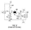
- Fig. 8shows a known down converter with a simple switch, as shown for example in "Semiconductor Circuitry" U. Tietze, CH Schenk, Springer-Verlag, 9th edition, 1989, Figure 18.37 on page 564.
- the buck converter in FIG. 8includes a ring-like interconnect with a coil 400, a capacitor 402, and a diode 404.
- the buck converter in FIG. 8further includes a charge switch 406 and a controller not shown in FIG configured to control the charging switch 406 so as to maintain the output voltage of the switching regulator, designated U SR in FIG. 8, at a defined level or in a range around the defined level.
- the circuit shown in Fig. 8comprises a certain number of nodes, which are set out below.
- a pole of an input voltage source U 0is connected, while at a second input node 412, another potential of the input source U 0 is connected.
- the second input node 412is typically the ground node.
- a first exit node 414is also referred to as a first output rail or positive output rail, while a second output node 416 is also referred to as a second output rail or negative output rail if the convention shown in FIG. 8 is used for the output voltage of the switching regulator U SR .
- the switch 406is connected on the one hand between the first input node 410 and a first intermediate node 418.
- the diode 404is connected between the first intermediate node 418 and the second input node 412 such that the anode of the diode is connected to the second input node 412, while the cathode of the diode is connected to the first intermediate node 418.
- the capacitor 402is connected between the first output node 414 and the second output node 416. According to the configuration of the diode, coil and capacitor network shown in FIG. 8, the coil is connected between the first intermediate node 418 and the first output node 414.
- the capacitor 402determines the ripple of the output voltage.
- the generation of the switching signal for switching the charging transistor 406is usually carried out by a pulse width modulator and a regulator with voltage reference.
- a reference voltagewhich supplies a desired value, is fed to a subtractor, to which the actual output voltage U SR is also supplied as an actual value.
- the output of the subtractoris fed to a variable gain amplifier which feeds a comparator, on the other hand, one generated by a sawtooth generator Signal is supplied.
- the output of the comparatoris the control signal for the switch 406 in Fig. 8.
- the variable gain amplifieris a PI control amplifier. It increases its output signal until the difference at the output of the subtractor becomes 0, until the output voltage U SR equals the desired output voltage.
- Typical magnitudes for dimensioning the coilare in the milli-Henry range (eg, 2.7 mH), while typical values for capacitors are in the three-digit micro Farad range (eg, 100 ⁇ F) when switching frequencies in the Range of 50 kHz can be used.
- Switching regulators shown in FIG. 8are intended to supply a suitable power supply to a subsequently connected circuit, such as an ASIC.
- the power supplyusually consists of one or more constant DC voltages of, for example, +5 V or ⁇ 15 V. Often this is not from the outset in the desired form available and must first by, for example, a switching regulator shown in Fig. 8, by a downstream linear regulator can be added to eliminate the ripple of the output voltage can be generated.
- On the input side of the switching regulator shown in Fig. 8is usually a rectifier, which generates the input voltage U 0 from the AC or three-phase network (230 V or 400 V) of the electric power plants.
- the switching regulatorrequires a choke (the inductance 400 in FIG. 8) which is relatively expensive to manufacture. However, this has only one winding and is thus easier to manufacture than a transformer having two windings. In addition, the choke can be reduced by choosing a higher working frequency, which also works with transformers.
- the voltage supply of the controller itselfis either via a separate voltage source or is generated from the input voltage, which means an additional voltage regulator and thus additional effort.
- the down-converter type switching regulator shown in Fig. 8which is also referred to in the art as a buck converter, as stated, relies on the charging switch 406 being turned on to charge the positive output node 414 against the negative output node 416. and then turn off the switch again, so to open, so that the output voltage does not exceed a set value range, which is determined by the mean value of the resulting output voltage U SR ultimately.
- Possibilities of controlling the switchare in principle to filter the output voltage to obtain an average of the output voltage without ripple, and then the charging switch on the basis of the filtered Control output voltage by a target / actual comparison.
- the output voltageis controlled by charging node 414 of capacitor 402
- US-B1-8465993discloses a control device for controlling a charging switch.
- the voltage detection signal or the error signalare filtered DC signals. Further, in US-B1-6465993, although the output voltage is detected, and further the current through the coil is detected.
- DE 19814681 A1shows a current-mode switching regulator with a first control device for voltage regulation and a second regulator device for load current control, each having two inputs and one output, wherein a first input of the first regulator means a reference signal and a second input as Controlled variable, an output signal of the current-mode switching regulator can be fed, and wherein the output of the first regulator means is coupled to a first input of the second regulator means.
- a controllable by a control signal of the second regulator circuit breakeris provided, the load path is arranged between a first pole with a first supply potential and a second pole with a second supply potential.
- a throttle deviceis arranged in series with this load path.
- an integratoris provided, which by temporal integration of the falling at the throttle device throttle voltage generates a control signal representing a load current, which is coupled as a controlled variable in a second input of the second regulator device. Through the integrator, the voltage drop across the inductor inductance is integrated over time to sense the current through the inductor.
- DE 19933039 A1discloses a device for generating a control signal for a DC-DC converter.
- the device for generating the control signalcomprises a voltage regulator and a current regulator. Between the voltage regulator and the current regulator, a limiter is provided, which serves to limit the output signal of the voltage regulator.
- the limitercomprises an input connection via which a specifiable limit value signal for the current setpoint can be input.
- the setpointis a fixed value, so to speak as a DC signal, while the actual value constantly fluctuates rapidly, which is an inherent property of the switching regulator, since the ripple of the output voltage as well as the ripple of the output current system arises by opening and closing the charging switch. Therefore, in these known regulator concepts, an actual value of either the voltage or the current must be filtered in order to obtain a filtered actual value having a DC voltage characteristic, such that a nominal / actual comparison with the setpoint present in "DC voltage characteristic" is feasible.
- the object of the present inventionis to provide a concept for controlling a charging switch in a switching regulator, which can be realized by a reduced circuit complexity.
- the present inventionis based on the finding that a setpoint / actual value comparison is not performed with a preset setpoint value, but that the "setpoint value" is actually generated in the control device.
- this setpoint / actual value comparisonis used only for opening the charging switch, ie for generating a high resistance in the charging switch, while the closing of the charging switch, so generating a low resistance in the charging switch clock-controlled, ie completely without setpoint / actual value -Comparison is performed.
- the switch-off controltakes place in that a first detection signal, which is representative of the output voltage, with a second detection signal for the current through the coil is representative, are compared. If the two detection signals have a predetermined relationship to each other, the charging switch is opened. In a subsequent clock of the clock, the charging switch is then closed again, and the capacitor of the switching regulator is recharged. Then, when the two detection signals, which are in fact both actual signals, are again in the predetermined relationship to each other, which may be, for example, an equality relationship, the charging switch is reopened, etc.
- either the current detection signal representative of the current flow through the coil or the voltage detection signal representative of the timing of the output voltageis inverted in such a way as to increase in the one to be detected Signal reflected in a decrease of the detection signal and vice versa.
- both signalsare actual values, which, however, due to the fact that one of the two is inverted, "adjust" to the effect that on average a constant coil current and a constant output voltage can be achieved. Which value the constant average output voltage will have depends on which voltage levels, or generally speaking signal levels, the two detection signals are brought to or how the predetermined relationship is defined.
- the target valueis thus set by transforming a level of the current flowing through the coil to, for example, a level of the current detection signal and transforming a level of the output voltage to the level of the voltage detection signal, and in particular the level conversion in FIG Detection of the current and the voltage, ie the current detection signal and the voltage detection signal to each other, takes place.
- the output voltage setpoint and the maximum coil currentcan be readily determined by sizing the resistors of the feedback operational amplifiers and by sizing the reference voltage, if not set to 0, can be achieved.
- the level of the mean output voltage or the average coil currentcan be realized by a special type of comparator. If the comparator is designed such that it does not supply a control signal in the case of the equality of the two detection signals but, for example, supplies a control signal when the two detection signals are separated from each other by a predetermined level, a voltage or current control can likewise be performed therewith ,
- the inductor current and the output voltageare therefore mapped into a voltage within a defined range, for example, so that the voltage increased increases as the inductor current increases, for example, but the output voltage decreases or decreases . vice versa.
- An independent clockthen switches the transistor of the switching regulator, whereupon the inductor current and thus also the current detection signal increases. As soon as the current detection signal intersects the voltage detection signal, the switch is turned off again. In terms of control technology, this can be represented in such a way that the current voltage detection signal, unfiltered, predefines the setpoint value for the maximum inductor current or vice versa.
- the present inventive control deviceis advantageous in that, on the one hand, the maximum current of the throttle is not exceeded is, since both detection signals, which are compared, have a determined by the switching regulator ripple. This is also advantageous in comparison to conventional regulators, since these regulators regulate the average inductor current, so that the maximum current can be significantly greater than the average current, as is the case, for example, in so-called gap operation. In contrast, in the circuit according to the invention due to the maximum control of the current "looked" directly to the current, which is currently present, so that parts of the switching regulator does not have to be "oversized” for a momentarily occurring much higher maximum current compared to the usual operation, ie the average current , which also reduces the cost of the Heidelbergreglercrofts invention.
- the control devicerequires neither a filter for filtering the current detection signal nor a filter for filtering the voltage detection signal. This also leads to a circuit simplification and thus to a price reduction. It should also be noted that the inventive concept over the prior art, in which the ripple of the output voltage is suppressed by a filter, positively uses this ripple, since it helps that the charging switch is turned off.
- control device concept of the inventionhas been found to result in the flow control loop being stable over a larger operating range. While in conventional controllers, the stable work area without further measures up to a duty cycle ranges to 50%, in the inventive concept of the range of stable current control can always be greater than 50% and theoretically extended by appropriate dimensioning up to 100%. Reasonable values for the practice have resulted in a stable operation with a duty factor of up to 80% to 90%.
- US-B1-6465993discloses a control device for controlling a charging switch, from which the subject-matter of claim 1 differs in that the node where the charging switch is coupled to the network is shorted to the output node. Instead, the node in US-B1-6465993 is connected via the coil to the output node at the screening capacity. As a result, in US-B1-6465993, the voltage detection signal or the error signal is filtered DC signals, while in the subject of the present invention, this is precisely not the case.
- US-B1-6465993further does not disclose a comparator as defined in claim 1. According to the invention, however, is compared by a comparator as defined in claim 1, the current detection signal with the voltage detection signal without further circumstances, error thresholds, error amplifiers, differential amplifiers or anything similar, however, one of the two signals, either the current detection signal or the voltage detection signal is inverted with respect to the quantity to be detected.
- controller 111 of the switching regulator according to the inventionBefore discussing in detail the controller 111 of the switching regulator according to the invention in FIG. 1, let us first consider the operating principle of a switching regulator which can be used alternatively to the switching regulator shown in FIG. 8 with a coil coupled to the anode of the diode and / or a changeover switch with voltage coupling means for driving the shown as a transistor charging switch.
- Fig. 1shows a preferred for the control according to the invention switching regulator for generating a regulated output voltage U SR using an input voltage U 0 , the sake of clarity as a voltage source U 0 10, which is connected in series with an internal resistance R i 12, is shown.
- a voltageis applied between a first input node 110 and a second input node 112.
- a controllable switch 106 and a network 101are connected in a manner that is serially connected to one another typical switching regulator network with a coil, a capacitor and a diode is.
- switching regulator networks 101also have a shunt resistor to provide a current path with a defined ohmic resistance.
- the output voltagewhich is controlled by the switching regulator shown in Fig. 1, is between a first output rail, which is also referred to as a positive output rail and is identical to the first output node 114, and a second output rail, which is also referred to as a negative output rail and identical to the second output node 116.
- the positive output rail 114can be brought to a first (positive) potential
- the negative output rail 116can be brought to a second potential which is smaller than the first potential.
- the network 101having a coil, a capacitor, and a diode, has, in particular, switched the diode to be coupled to the positive output rail when the coil is coupled to the negative output rail or to be coupled to the negative output rail when the coil is coupled to the positive output rail.
- the diodewill thus be coupled to an output rail, either the positive output rail 114 or the negative output rail 116.
- the switch 106 shown in FIG. 1is also referred to as a charging switch since it is provided for charging the capacitor in the network 101. In particular he is in Series connected to the diode.
- the charging switchfurther comprises a control input 107, via which the charging switch 106 can be closed, which means that the input voltage does not drop at the charging switch, but at the network 101. If the switch is opened, the input voltage drops across the switch, the network 101 is thus (apart from transient states) not charged with the input voltage.
- the network 101further comprises a capacitor, which is also referred to as a filter capacitor and is connected in such a way that the regulated output voltage can be tapped off at the capacitor.
- An essential part of the network 101is also the inductance, which is also referred to below as a coil, which is coupled on the one hand with the diode and on the other hand with the capacitor.
- the switching regulator shown in FIG. 1further has a switching device 109, which is controllable, depending on a switching control signal provided by a controller 111, either the first output rail 114 or the second output rail 116 via a coupling device 113 with the control input 107 of Charging switch to couple.
- the charging switch 106is formed such that it is closed due to a potential at an output rail, and is opened due to a potential at the other output rail.
- the charging switch 106as will be shown later with reference to FIGS. 2 and 3a, is designed as a self-conducting or self-blocking NMOS transistor. In this case, the charging switch 106 is closed (turned on) by the potential at the positive output rail while being opened (idled) by the potential at the negative output rail.
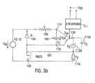
- the coil 100 and possibly the shunt resistor 101will be switched between the nodes 118 and 114 and the nodes 112 and 116 will be short-circuited and the potential at the negative output rail will be used for this, to open the switch while the potential on the positive output rail 114 is used to close the switch 106, ie to bring it into idle mode, while the potential at the positive output rail is used to close the switch 106.
- a corresponding circuitis shown in Fig. 3b.
- the controller 111will include a controller which may be of any configuration as long as it outputs a signal that causes the output voltage U SR to have a defined desired timing by opening and closing the charging switch 106.
- the controller 111will operate to ensure an output voltage with an average at the output 114, 116 of the network 101, regardless of which load is on or what current is drawing a load.
- the time course of the voltage U SRwill typically be a voltage waveform with some ripple around an average.
- the ripplecan be brought into predetermined tolerance ranges by dimensioning coil and capacitor, in many cases, a signal with a ripple around an average is already sufficient, namely In particular, when the requirements of the switching regulator output signal, ie the voltage U SR , are not very high, such as for a lamp or something similar.
- the switching regulator as shown in Fig. 1is integrated on a substrate together with an integrated circuit to be supplied by it, it will be supplemented by a linear regulator downstream of the output 114, 116 of the switching regulator to meet requirements for a voltage U SR that exceed the capabilities of the switching regulator shown in Fig. 1, to provide a reasonable output an output signal U SR with appropriate specification.
- the on / off controlis performed such that when the controller 111 determines that the charging switch is to be opened, the changeover switch 109 is connected to the output rail associated with the opening of the charging switch 106, for example 116 in FIG when the charging switch 106 is to be closed because the capacitor in the network 101 is to be recharged, the controller 111 activates the switch 109 to now couple the potential of the upper output rail 114 to the control input 107 of the charging switch 106.
- FIG. 2shows an exemplary embodiment in which the coil 100 is connected to the diode 104 and the filter capacitor 102. Comparing FIGS. 2 and 8, it will be seen that the coil 100 is no longer connected to the cathode of the diode 104, as in FIG. 8, but is connected to the anode of the diode 104. Furthermore, it can be seen from the comparison of FIGS. 2 and 8 that now the positive Output rail 114 with an intermediate node 118, via which the charging switch 106 is connected to the diode 104, coincides with the output node 114, so the first output rail coincides. Further, a shunt resistor R sh 101 is shown in Fig. 2, which is connected between the coil 100 and the negative output rail 116. A node 103 between the shunt resistor 101 and the coil 100 is also referred to as a lower intermediate node.
- the charging switch 106is designed as a self-blocking NMOS transistor whose drain D is connected to the first input node 110 and whose source S is first short-circuited to a bulk terminal B of the transistor, and its source S further directly coupled to the positive output node 114, so the positive output rail.
- the coupling device 113 of FIG. 1comprises a Zener diode D Z 113a, a capacitor C Z 113b connected in parallel, and a series resistor R Z 113c.
- the ballast resistorserves to provide power to the parallel connection of the capacitor 113b and the diode 113a via the first input node 110 forming a voltage dropping device, as will be explained later.
- the transient characteristics of the storage elements coil L and capacitor C Sare important for the operation of the switching elements shown in FIG. 2, since the switching regulator, as shown in FIG. Turning off the charging switch 106 reached.
- a coilis characterized in that the voltage dropped across the coil is equal to the time derivative of the current flowing through the coil. Accordingly, a capacitor is characterized in that the current flowing through the capacitor is proportional to the time derivative of the voltage across the capacitor.
- the voltage applied to the coilcan jump, but that the current through the coil can not jump. Therefore, if a coil is turned on, so a DC voltage is applied (via a source internal resistance) to the coil, the voltage across the coil abruptly increases to the value of the applied DC voltage and then drops exponentially. At the same time, the current through the coil begins to increase slowly from its original value 0 until it eventually reaches a value equal to the quotient of the applied voltage and the internal resistance of the source. When this stationary time is reached, the voltage dropped across the coil has also become zero.
- the elements coil and capacitorthus differ in that the current can jump through the capacitor while the voltage on the coil can jump.
- the voltage across the capacitorcan not jump.
- a coil through which a current flowsis switched off, it is again important how the coil is switched off. If a current flows through a coil, there is a magnetic field in which energy is stored. If a coil is separated from the source by idling between source and coil, then the current through the coil would actually be suddenly brought to zero. However, the stored energy in the magnetic field of the coil must be able to drain. Therefore, turning off a coil by creating an open circuit between the source and the coil results in a high voltage spike, which causes the switch to form an arc that allows the energy stored in the magnetic field to flow to the source. Because of this, a coil becomes the theoretically infinitely high voltage spikes that would be destructive, avoid discharging through a resistor, a diode or a capacitor. This leads to a spike with reduced height. If a coil is switched off, the voltage arrow and the current arrow point in different directions again. The coil thus works as a generator.
- the coilis connected in series with a capacitor, so at the turn-on, so when a voltage of 0 is changed to a voltage with a certain DC value, the capacitor is a Short circuit and the coil is idling.
- the entire voltageis initially applied to the coil and then decreases with increasing current through the series resonant circuit of coil and capacitor.
- the coilstill generates a current that continues to flow for some time until the energy stored in the coil has drained away.
- the energy from the coilis then in the capacitor, ie the voltage U C is equal to zero.
- the current through the coil 100is equal to the current flowing to the load between the positive output rail 114 and the negative output rail 116 is turned on.
- the chokefeeds the capacitor via the freewheeling diode.
- the inductor currentis greater than the load current, the voltage on the capacitor increases. The more energy that passes from the throttle to the capacitor, the smaller the inductor current. Eventually, the inductor current will be smaller than the load current and from this point on, the voltage across the capacitor will drop.
- the switchIn order to avoid an excessive drop in the voltage, the switch must be turned on again, so that the inductor current increases again. However, the inductor current at the time of switching on is still lower than the load current, so that the voltage at the capacitor initially continues to decrease. With a conductive switch, however, the inductor current now increases again and eventually becomes larger again than the load current. From this point the voltage on the capacitor increases again. Now, if the current through the throttle is too large, then the switch is disabled again, and the current through the throttle is again lower. The cycle starts all over again.
- the switch 106at the time the switch 106 is turned on, the full voltage is applied to the diode 104 and, as stated above, the voltage on the capacitor can not jump but can jump on the coil simultaneously with the switch-on time, the potential of the negative output rail 116 is also raised.
- the controller 111will operate the switch 109 such that it is no longer connected to the positive output rail 114 but to the negative output rail 116. This will cause the transistor 106 to turn off and no more current from the source 10, 12 to flow into the coil, diode, and capacitor network. This causes the coil to act as a generator, in that the potential at node 103 drops and the coil provides a current that continues to charge capacitor 102 through diode 104, so that after turning off the capacitor Wegers the voltage U SR rises a little further. This increase is slowed down by the current flowing across the load and, when the current drawn by the load becomes smaller than the current that the coil 100 supplies to the node 114, becomes a voltage drop.
- the switch 106 shown in Fig. 2ais designed in this embodiment as a self-blocking NMOS transistor.
- NMOS transistorsconduct when the voltage between the gate, so the control terminal 107 and the source is greater than a possibly existing threshold voltage.
- the coupling device 113 of FIG. 1comprises the elements ballast resistor 113c, parallel capacitor 113b and Zener diode 113a shown in FIG. 2a.
- the zener diode 113ais configured to operate as a voltage source from a certain breakdown voltage that is fixedly configured, which means in other words, that at the parallel circuit of capacitor 113b and diode 113a, the breakdown voltage U .through the zener diode is always determined Z drops off. If the switch 109 to the positive rail 114, so the voltage dropped across the Zener diode voltage U Z lies directly between the gate and source of the transistor. The control input 107 of the transistor is thus coupled to the positive output rail via the parallel circuit of capacitor and zener diode, to the effect that the transistor becomes conductive.
- the breakdown voltage determined by the Zener diodeis greater than the threshold voltage of the transistor.
- this requirementis readily met because transistor threshold voltages are typically not very large and Zener diodes with different defined breakdown voltages are present.
- the Zener diodeonly has to be tuned very loosely to the transistor since the value of the breakdown voltage of the Zener diode only has to be greater than the threshold voltage U th of the transistor.
- the threshold voltage requirements of transistor 106 and the breakdown voltage of diode 113aare very low in terms of the required tolerance.
- the illustrated conceptis thus particularly advantageous in that the reject rate and thus the cost of the final product can be kept low.
- the controllerdetermines that the switch 105 is to be turned off again, it controls the changeover switch 109 so that it is connected to the negative output rail. As a result, the potential at the gate 107 of the transistor becomes smaller by U SR than in the switched-on state. This will lock the transistor.
- a particular advantage of the circuit shown in Fig. 2is that a defined start-up of the circuit is ensured. For the defined start it is particularly irrelevant whether the changeover switch 109 at the time of switching on with the positive output rail 114 or the negative output rail 116 is connected. In particular, when the switch 109 is implemented as a multiplexer of transistors or as an inverter, it is undefined whether the switch 109 is connected to the upper rail 114 or the lower rail 116, if it is assumed that the entire circuit shown in FIG. 2 circuit was in a de-energized state, so that all potentials in the circuit are at the value 0.
- the changeover switch 109is connected to the negative rail 116, then the capacitor 113b likewise charges via the series resistor R Z.
- the potential at node 118which determines the source potential of the transistor is not initially brought out of its 0 value, since no charge of the capacitor 102, through which the potential 118 could be raised, takes place, since the switch 109 with the negative rail 116 is connected.
- the gate-to-source voltageincreases from a value of 0 at the time the source 10, 12 is turned on by actuating the switch 14 in FIG. 1 to a value equal to the threshold voltage of the transistor is.
- the drain-source path of this switch 106becomes conductive, and the capacitor C S is charged (regardless of the position of the switch 109).
- the charging current for the capacitor 102 (C S )flows simultaneously via the coil 100 to the ground 112. This leads directly to the fact that the output voltage U SR increases due to the increase of the potential at the positive output rail 114 against the potential at the negative output rail 116. This charging process continues until the voltage across the capacitor C s reaches the voltage at the Zener diode minus the threshold voltage of the switch 106.
- this "remaining value" of the output voltage U SRis relatively freely selectable.
- the Zener diodeis sized so that U SR becomes so large (when in "unfavorable If the change-over switch 109 is connected to the negative rail 116 for start-up, the controller 111, which is preferably supplied by U SR , can already work, and the voltage U SR is thus determined by dimensioning the Zener diode (and the threshold voltage). made so large that when this voltage is applied to the controller, the states at the nodes in the controller are already defined.
- the controllerwill therefore detect a value U SR and compare it to a limit. Once the controller determines that U SR has reached the predetermined state at power-up, the controller 111 operates to ensure that the switch 109 is connected to the positive rail 114. If this was already the case during startup, the controller 111 does not change the changeover switch 109 here. If this was not the case, however, so at the time of starting the switch 109, as shown in Fig. 2, connected to the negative rail 116, the controller will control the switch 109 such that now no longer the negative rail 116 at the control terminal 107 is coupled, but that the positive rail 114 is coupled to the control input 107. This is the potential of the positive output rail at the anode of the Zener diode.
- the voltage on the filter capacitor C S 102continues to increase due to the charging current flowing through the charging switch 106 until a desired output voltage is applied to C S.
- the changeover switch 109is switched back and forth by the controller 111 to turn the switch T on and off, and thereby the output voltage U SR according to voltage and current demand of a load (in Fig. 2 not shown).
- the circuit shown in Fig. 2is thus particularly advantageous in that it starts up in a defined manner, wherein it is irrelevant at the time of startup, in which position the switch 109 is. Furthermore, it is preferred to dimension the controller 111 such that it already operates in a defined manner when the output voltage is equal to the zener diode voltage U Z minus the threshold voltage of the transistor 107. Thus, the startup process can be continued defined without own supply for the controller 111. This leads in particular to a low-cost circuit, since no special start-up measures must be taken, except to ensure that the changeover switch 109 is connected to the positive rail 114. After no special measures are required and in particular voltage checks with regard to the control 111, etc. must be performed, the boot-up process takes place very quickly.
- the voltage increasecan be dimensioned very quickly by appropriate dimensioning of the resistor 113c and the capacitor 113b.
- the resistor 113cit is anyway preferred to dimension the resistor 113c relatively large, so that the power loss generated by it does not come in significant orders of magnitude.
- the capacitor C Zwhich anyway only serves to stabilize the Zener diode 113a or to its (small) junction capacitance, so that it is quickly charged to the voltage U Z. The startup thus takes place in such a way that no time constants would have to be taken into account, which would significantly slow down the startup of the switching regulator.
- FIG. 3ashows an alternative exemplary embodiment, which differs from FIG. 2 in that the transistor T 106 is now a self-conducting NMOS transistor, and that the coupling device 113 of FIG. 1, which in FIG. 2 is represented by the elements 113 a, 113b, 113c was realized in Fig. 3a by a simple coupling 113d. While the potential at the first output rail or the second output rail has been subjected to a voltage drop via the coupling device 113 in FIG. 2, the potential at the first output rail 114 or the second output rail 116 is directly connected to the first output rail 114 or the second output rail 116 in FIG Control terminal 107 of the switch 106 coupled.
- Transistor 106is implemented as a normally-on n-channel MOSFET or n-channel JFET. The wiring of the transistor forming the charging switch 106 with respect to drain and source is identical to the case of FIG. 2.
- the threshold voltage of the transistor U This dimensioned to be equal to the Z voltage of the Zener diode minus the threshold voltage of the normally-off MOSFET in the first case for the output voltage U SR to reach such a value in the startup process , by which the controller 111 is already operable to be able to control the switch 109 at a certain time of the start-up process in such a way that it is connected to the positive rail 114 in a defined manner.
- Threshold voltages in self-conducting NMOS transistors or N-JFET transistorsare defined as defining a negative voltage between the gate and source of the transistor at which transistor 106 is blocking. Voltages that are higher than the negative threshold voltage will then cause the transistor to conduct, while voltages even more negative than the threshold voltage will cause the transistor to turn off.
- the threshold voltage of the transistor 106is selected such that an output voltage U SR then present at the output is already sufficiently high to allow the controller 111, which is supplied with the voltage U SR , to operate in a defined manner. so that it then separates the switch 109 from the negative rail 116 and connects to the positive rail 114, so that the transistor is opened again, so that the charging of the capacitor 102 can be continued until the controller 111 goes into normal operation and a Switch control due to an actual desired output voltage U SR makes.
- the boot-up process in FIG. 3ais thus such that initially the switch T is conducting.
- the capacitor 102is charged via the switch T and the inductor L until the voltage across the capacitor C S reaches the threshold voltage of the switch T (when the switch 109 is connected to the negative rail 116 was).
- the voltage at the output of the circuit U SRalready so large that a controlled work of the regulator is guaranteed.
- the voltagecontinues to increase at C S until the desired output voltage is applied to C S.
- the switch Tis turned on and off, whereby the output voltage U SR is controlled.
- the threshold voltage of the transistor 106 in the case of Fig. 3a or the threshold voltage of the transistor 106 and the Zener diode voltage U Z of Fig. 2it should be noted that these values are dimensioned so that the controller 111 in the automatic without intervention in the circuit and in the preselected position of the changeover switch 109 on the negative rail 116, the maximum output voltage value U SR , which is self-evident without any intervention, has already reached such a level that the control can be supplied with U SR .
- the controller 111 or the threshold voltage or the threshold voltage and the Zener diode voltageare dimensioned such that the output voltage U SR , which is reached " automatically", is already slightly higher than the voltage at which the controller 111 operates defined.
- the controller 111may also be configured to immediately, if it can work defined, so if the input voltage is sufficiently large, the switch 109 upwards, so put on the positive output rail. So the switching time is not limited to that always the maximum automatically achievable output voltage must be present to switch the switch. Instead, it is necessary that at some point in the startup process it is ensured that the changeover switch is connected to the positive output rail 114.
- the coilis not coupled, as in FIG. 7, to the cathode of the diode, but to the anode.
- Thishas the advantage that, when the switch 109 is connected to the positive rail 114, the potential generated between the gate and source of the transistor is not affected by the transient characteristics of the coil.
- the coilmay in another embodiment also be coupled to the diode cathode side, such that then the switching device 109 when it connects the positive rail to the transistor gate 107, so to speak, either directly couples the coil to the gate of the transistor or short-circuits or indirectly coupled via a voltage dropping device.
- An arrangement of the coil on the anode side to the diodefurther has the advantage that then limits the input voltage of the circuit only by the dielectric strength of the three elements switch, diode and throttle.
- the switching regulatoritself is self-powered and runs up in a defined manner. The jumping of the common mode potential of the output voltage between the positive and negative rails of the input voltage depending on the state of the switch T is not of primary importance to the load, since it does not notice this jumping because the load only the potential difference between the upper output rail and the lower output rail experiences, but not the "absolute" potential of the positive output rail or the negative output rail for themselves.
- the start-up timeitself is defined by the sizing of R Z and C Z , the inductance of the inductor L and the capacitance of the sieve capacitor C s . An additional start-up delay to ensure the voltage supply of the regulator is not needed.
- the input voltage rangewhich is usually limited to an input voltage ratio of U E, max / U E, min ⁇ 5: 1, can be increased to at least 50: 1, as long as possible the dielectric strength of the diode, the coil and the switch is carried accordingly, since these elements are acted upon by the input voltage.
- neither the capacitor nor the switch nor the controllerare subjected to such high voltages, so that for these elements, the maximum input voltage need not be taken into account, which in turn leads to a cheaper and more flexible Heidelbergreglerbib.
- FIG. 4is a detailed illustration of the controller 111 according to one embodiment of the present invention, which may either be used to drive the switch 109 when the charge switch 106 is a transistor, or which may be used to directly drive the switch 106. when the switch 106 is any switch that can be opened or closed by different control signals.
- This alternative to the control of a charging switchis shown in FIG. 4 with a dashed line 119. It can be seen that the controller 111 according to the invention shown in FIG. 4 can also be used to control the general charging switch 406 in FIG. 8 for the known Buck controller.
- the controller 111is coupled to the network 101 having the coil, the capacitance, and the inductor, as schematically represented by a coupling device 1110.
- the control according to the inventioncomprises an output voltage detection device 1111 for generating the output voltage U SR between the positive output rail 114 and the negative output rail 116 or between the positive output node 414 and the negative output node 416 of FIG. 8.
- an inductance current detection device 1112is provided is formed to detect the current through the coil or inductance in the network 101. It can be shown that the current through the coil in the network 101 is on average equal to the current through a load coupled to the positive output rail 114 and negative output rail 116 which, as shown in FIG. 8 by the load 408, is supplied by the regulated voltage U SR .
- the output voltage detector 1111is configured to provide a voltage detection signal on the output side. Accordingly, the inductance current detecting means 1112 is configured to provide a current detection signal on the output side.
- the voltage detection signal and the current detection signalare fed to a comparator 1113, which is operative to detect whether or not a predetermined relationship exists between the voltage detection signal and the current detection signal.
- the comparator 1113is configured to provide, when there is a predetermined relationship between the two signals, a switch-on signal 1114 to a switch actuator 1115.
- the switch actuator 1115which is provided to drive the charging switch either directly via the dashed path 1119 or indirectly via the switch 109, is further coupled to a clock 1116 which provides, on the output side, a clock signal which acts as a switch-to signal 1117 ,
- the output voltage detecting means 1111is configured to provide a voltage detection signal which then rises in level when the level of the output voltage drops, and which conversely then falls in level as the output voltage increases.
- the voltage detection signalhas a relation to the output voltage to be detected inverted timing, so that with increasing output voltage, the voltage detection signal falls and vice versa.
- the output voltage detector 1111that must provide the inverse-time detected detection signal, but that can be accomplished by the inductor current detector 1112 as well. However, due to the particular circuit configuration illustrated in FIG. 5, it is preferred that the output voltage detector 1111 provide an inverted timing detection signal to minimize the number of elements used.
- the comparator 1113is formed in a preferred embodiment of the present invention to determine whether the voltage detection signal and the current detection signal have the same level. Further, for example, when the two input signals to be compared are equal, the comparator outputs a voltage pulse, while the comparator outputs nothing when the two signals to be compared are not equal. Alternatively, however, the comparator could also be designed to be equal in case of equality output a first voltage level and, in the case of equality, a second larger or smaller voltage level. Again alternatively, the comparator could also be designed to generate in the case of equality a rising signal edge in its output voltage, while in the case of inequality a falling signal edge is generated and vice versa.
- the comparatorcould also be designed not only to output a signal indicating the equality of the input signals to be compared, but additionally to indicate which of the two signals is greater or which of the signals is smaller.
- the comparatorcould also be designed not only to output a signal indicating the equality of the input signals to be compared, but additionally to indicate which of the two signals is greater or which of the signals is smaller.
- FIG. 6it is known from the outset which signal is larger, and which signal is smaller, due to the typical course of the voltage detection signal and the current detection signal to each other.
- thisis not the case when unforeseen load transients affect the output voltage sense signal.
- the switch actuator 1115operates to generate a control signal on the output side to close the switch, that is, to make it low, and to open the switch 106, that is, to make it high-resistance.
- the switch closureis effected by the clock 1116, such that the switch actuator 1115 is operative to drive the switch 106 to a particular event in one clock period of the signal generated by the clock 1117 so that it is closed, whereas if the Switch was closed, the same is opened again when the comparator from a switch-on signal 1114 of the switch driver 1115 has been obtained.
- the switch driver 1115may, for example, B. interpret a positive clock edge as a switch-to signal. Alternatively, a negative clock edge can also be interpreted as a switch-to-signal. Depending on the implementation of the switch driver 1115 could also z. B. the second, third, etc. rising or falling edge are interpreted as a switch-to signal.
- the switch driver 1115is thus configured to interpret an event in the clock provided by the clock 1116 as a switch-to signal 1117 such that upon detection of this signal, a corresponding pulse from the switch driver 1115 to the switch 109 or is delivered directly to the charging switch 106. If the clock generator already generates a clock signal with correct voltage ratios, the switch driver 1115 may be operative to simply switch this signal on and apply it to the changeover switch 109 or to the dashed bypass line 119 to drive the switch 106 directly.
- Fig. 5shows a preferred embodiment of the controller 111 of Fig. 4.
- the inductor current sensing means 1112 of Fig. 4comprises a first current measuring resistor 11120, a feedback resistor R 1 11121, a first operational amplifier OV1 11122, and a reference voltage source 11123.
- One not with the negative output rail 116 connected node of the reference voltage source 11123is connected to a positive input of the operational amplifier 11122 connected.
- a node to which the feedback resistor 11121 and the current sense resistor 11120 are coupledis connected to a negative input, that is, the minus input of the operational amplifier 11122.
- the output voltage detecting means 11111 of Fig. 4comprises first a voltage divider having a first resistor R 4 11110 and a second resistor R 5 11111. Further, the output voltage detecting means also comprises an operational amplifier OV2 11112 and a feedback resistor R 3 11113. The node at which the resistor R 4 11110 and the resistor R 5 11111 are connected to the feedback resistor R 3 11113 is connected to a negative or negative input of the operational amplifier OV2 11112, while the node of the reference voltage source 11123, which is not connected to the negative output rail 116, with the positive input or positive input of the operational amplifier OV 2 11112 is connected.
- the elements with the leading numerals "1111”thus form the output voltage detector 1111 of FIG. 4, while the elements with the leading numerals "1112” form the inductance current detector 1112 of FIG. It should be noted that the reference voltage source is used both within the inductor current detector 1112 and in the output voltage detector 1111.
- the current detection signal U Dais a signal which is directly proportional to the course of the current I D through the inductance 100. This is the case because the current I D or a current i R2 flowing due to the resistance ratios of R sh and R 2 is directly proportional to the current through the inductance 100 I D.
- a first signal curve 601shows a schematically shown time characteristic of the output voltage U A or U SR .
- the reference numeral 602indicates the waveform of the voltage detection signal U Aa 1119 which, as can be seen from FIG. 6, is negatively proportional to U A. In other words, this means that when U A rises, the voltage U Aa 602 drops and vice versa. Further, in Fig. 6 at 603 the current detection signal U Da drawn, which is directly proportional to the current through the coil 100.
- the reference numeral 604designates the control signal U St , which is also denoted by 1120 in FIG. 5 or FIG. 4, the dimensioning of the changeover switch 109, for example, or the charging switch 106 being such that the switch is closed when the control signal 604 has a high potential, So is turned on, while at low potential of the signal 604, the switch is open, so is very high impedance.
- Fig. 6also shows the state of the reset input of the register 1115, which is preferably used as the switch driving means.
- the register 1115will be explained below with reference to FIG. 7.
- the reset state of the registeris the state of the output that sets after the reset input is activated. This is usually the "low" state.
- FIG. 6shows a schematic time characteristic of a comparator output signal originating from a comparator 1113 which, when the equality condition is satisfied, outputs a voltage pulse, which is drawn in FIG. 6 by way of example as a direct pulse.
- the course of the comparator output voltage U kis designated 606 in FIG. 6.
- FIG. 6also shows the time characteristic of the clock ⁇ 607 in temporal synchronism with the signals 601 to 606.
- the output voltagewhich is only sketchily represented by the time characteristic 601 with regard to its rise characteristics and fall characteristics, drops further for a while at the time the clock is switched on as long as the inductor current is smaller than the load current. Since the inductor current rises after switching on, it eventually becomes larger than the load current, whereby the voltage U SR at C S increases again. When the current reaches the value demanded by the controller, the comparison of the comparator causes the switch to be switched off. As a result, the inductor current decreases again. However, the voltage U SR continues to increase as long as the inductor current is greater than the load current. If the inductor current drops below the load current, then begins the tension to fall again. Another clock pulse restarts the cycle described above.
- the voltage detection signal U Aahas a waveform inverted from the output voltage signal U A so that the output voltage detection signal 602 has a maximum when the output voltage signal has a minimum, and vice versa.
- the reset stateremains until the comparator returns to a comparator signal at a time t 3 at which the profile of the voltage detection signal 602 again intersects the profile of the current detection signal 603 is given to the register 1115 such that the reset state as shown by the timing 605 is terminated at the register.
- the registeris then ready after the time t 3 again to bring the Q output in a high state, if at the S input again z. B. a positive clock edge due to the clock 607 is applied.
- Register 1115is thus disabled in the time period from t 2 to t 3 in the preferred embodiment of the present invention, ensuring in each case that the switch remains off.
- the actual turn-off timeis longer than the time period between t 2 and t 3 .
- the reset state of the registeris present when the voltage detection signal is lower in level than the current detection signal.
- the reset input signalis not active.
- a control of the switchis effected when the voltage detection signal 602 is greater than the current detection signal 603.
- the register 115is particularly preferred because, when the operating clock frequency f T is not dimensioned such that per each clock period T T, the controller is turned on once, prevents a switching of the clock, for example, if the output voltage has not fallen so far again is that it would need to be increased again, or that another stream from source 10, 12 is needed. This is because when the voltage detection signal 602 is smaller than the current detection signal 603, the register remains in the reset state and thus a positive clock edge that would cause the controller to turn on in the non-reset state is not passed, so that no excessive increase of the output voltage U A is achieved by continuous switching on of the regulator, although the output load does not need to be supplied further.
- the duty cycleie the time period between t 2 and t 1 based on the clock period T T , less than 50% is selected. From Fig. 6, however, it can be seen that the cycle time can easily be increased without causing problems. An increase in the time duration between t 1 and t 2 causes the switch remains closed longer, so that more energy per clock from the source 10, 12 the switching regulator (and thus the load) is supplied. A decreasing output voltage, ie an overall "vertical shift" of the output voltage profile U A downwards, as indicated by an arrow 610, would lead directly to an overall "vertical rise" of the signal 602 due to the inverting generation of the voltage detection signal, as indicated by a Arrow 611 indicated is.
- the current waveformdoes not change as the output voltage changes. This is not the case in practice, but serves to understand the functionality of the invention.
- the waveform of the voltage detection signal 602is raised, the trace of the voltage sense signal will also intersect a dashed continuation of the waveform, labeled 612, at some point.
- the regulator according to the inventionis designed to reopen the switch whenever it has an intersection between voltage detection signal 602 (which has been pushed upwards in accordance with arrow 611) and dashed continuation 612 of the current profile.
- a further advantageis that the voltage amplifier, which generates the image of the output voltage, that is, the operational amplifier 11112 with corresponding circuitry, does not need a filter at the output since the ripple does not disturb the output voltage but has a positive effect.
- the components operational amplifier, comparator, registers and reference voltage sourcewhich could optionally be omitted, are components that can all work with relatively low operating voltages, so that even when starting from a certain value of the output voltage U SR , the is still lower than the operating output voltage to be generated by the switching regulator, a stable and defined operation takes place.
- the number of componentsis reduced.
- the control device according to the inventionin particular with regard to the reduced number of components (here is also the otherwise required filter for filtering the actual size to call) are inexpensively manufactured in particular integrable execution.
- the method according to the invention for controlling a charging switch in a switching regulatorcan be implemented in hardware or in software.
- the implementationmay be on a digital storage medium, in particular a floppy disk or CD with electronic readable control signals, which can cooperate with a programmable computer system so that the inventive method is performed.
- the inventionthus also consists in a computer program product with a program code stored on a machine-readable carrier for carrying out the method according to the invention, when the computer program product runs on a computer.
- the inventioncan thus be realized as a computer program with a program code for carrying out the method when the computer program runs on a computer.
Landscapes
- Engineering & Computer Science (AREA)
- Power Engineering (AREA)
- Dc-Dc Converters (AREA)
- Charge And Discharge Circuits For Batteries Or The Like (AREA)
Abstract
Description
Translated fromGermanDie vorliegende Erfindung bezieht sich auf Schaltregler und insbesondere auf das Steuern eines Ladeschalters eines Schaltreglers mit einer Induktivität, einer Siebkapazität und einer Diode.The present invention relates to switching regulators and, more particularly, to controlling a charging switch of a switching regulator having an inductance, a screening capacitance and a diode.
Fig. 8 zeigt einen bekannten Abwärts-Wandler mit einem einfachen Schalter, wie er beispielsweise in "Halbleiterschaltungstechnik" U. Tietze, C.H. Schenk, Springer-Verlag, 9. Auflage, 1989, Abbildung 18.37 auf Seite 564 gezeigt ist. Der Abwärts-Wandler in Fig. 8 umfasst eine ringartige Verschaltung mit einer Spule 400, einem Kondensator 402 und einer Diode 404. Der Abwärts-Wandler bzw. Schaltregler in Fig. 8 umfasst ferner einen Ladeschalter 406 sowie eine in Fig. 8 nicht gezeigte Steuerung, die ausgebildet ist, um den Ladeschalter 406 so zu steuern, dass die Ausgangsspannung des Schaltreglers, die in Fig. 8 mit USR bezeichnet ist, auf einem definierten Niveau zu halten bzw. in einem Bereich um das definierte Niveau herum zu halten.Fig. 8 shows a known down converter with a simple switch, as shown for example in "Semiconductor Circuitry" U. Tietze, CH Schenk, Springer-Verlag, 9th edition, 1989, Figure 18.37 on page 564. The buck converter in FIG. 8 includes a ring-like interconnect with a
Die in Fig. 8 gezeigte Schaltung umfasst eine bestimmte Anzahl von Knoten, die nachfolgend dargelegt werden. An einem ersten Eingangsknoten 410 der Schaltung wird ein Pol einer Eingangsspannungsquelle U0 angeschlossen, während an einem zweiten Eingangsknoten 412 ein anderes Potential der Eingangsquelle U0 angeschlossen wird. Der zweite Eingangsknoten 412 ist typischerweise der Masseknoten. Ein erster Ausgangsknoten 414 wird auch als erste Ausgangsschiene oder positive Ausgangsschiene bezeichnet, während ein zweiter Ausgangsknoten 416 auch als zweite Ausgangsschiene bzw. negative Ausgangsschiene bezeichnet wird, wenn die in Fig. 8 gezeigte Konventioh für die Ausgangsspannung des Schaltreglers USR verwendet wird. Der Schalter 406 ist einerseits zwischen den ersten Eingangsknoten 410 und einen ersten Zwischenknoten 418 geschaltet. Ferner ist die Diode 404 so zwischen den ersten Zwischenknoten 418 und den zweiten Eingangsknoten 412 geschaltet, dass die Anode der Diode mit dem zweiten Eingangsknoten 412 verbunden ist, während die Kathode der Diode mit dem ersten Zwischenknoten 418 verbunden ist. Ferner ist, wie es in Fig. 8 gezeigt ist, der Kondensator 402 zwischen den ersten Ausgangsknoten 414 und den zweiten Ausgangsknoten 416 geschaltet. Gemäß der in Fig. 8 gezeigten Konfiguration des Netzwerkes aus Diode, Spule und Kondensator ist die Spule zwischen den ersten Zwischenknoten 418 und den ersten Ausgangsknoten 414 geschaltet.The circuit shown in Fig. 8 comprises a certain number of nodes, which are set out below. At a
Nachfolgend wird auf die Funktionalität der in Fig. 8 gezeigten Schaltung eingegangen. So lange der Schalter 406 geschlossen ist, wird UD gleich der negativen Eingangsspannung U0. Wenn er sich öffnet, behält der Drosselstrom IL seine Richtung bei, und UD sinkt betragsmäßig ab, bis die Diode leitend wird, also ungefähr auf 0-Potential. Der zeitliche Verlauf des Spulenstroms ergibt sich aus dem Induktionsgesetz, gemäß dem die Spannung an der Spule gleich dem Produkt aus der Induktivität L der Spule und der Ableitung des Spulenstroms nach der Zeit ist. Während der Einschaltzeit, also wenn die Eingangsspannung U0 an der Diode 404 anliegt, liegt an der Drossel die Spannung U0 - USR an. Während der Ausschaltzeit taus des Schalters 406 liegt an der Drossel die Spannung UL = -USR an. Daraus ergibt sich eine betragsmäßige Stromänderung ΔIL, die folgendermaßen gegeben ist:
Aus dieser Bilanz lässt sich wiederum die Ausgangsspannung berechnen, die folgendermaßen definiert ist:
In der vorstehenden Gleichung ist T = tein + taus = 1/F die Schwingungsdauer, und p = tein/T ist das sogenannte Tastverhältnis. Es ist zu sehen, dass sich als Ausgangsspannung erwartungsgemäß der arithmetische Mittelwert von UD ergibt. Typischerweise wird die Induktivität L der Spule 400 so gewählt, dass ein Minimalstrom nicht unterschritten wird, wie es in der Technik bekannt ist. Ferner ist bekannt, dass mit Erhöhung der Taktfrequenz die Induktivität verkleinert werden kann. Ferner steigt bei zu hohen Frequenzen der Aufwand für den Schalttransistor und die Ansteuerschaltung. Außerdem nehmen dynamische Schaltverluste proportional zur Frequenz zu.In the above equation T = ton + toff = 1 / F, the oscillation period, and p = ton / T is the so-called duty cycle. It can be seen that, as expected, the arithmetic mean of UD is the output voltage. Typically, the inductance L of the
Der Kondensator 402 bestimmt die Welligkeit der Ausgangsspannung. Die Erzeugung des Schaltsignals zum Schalten des Lade-Transistors 406 erfolgt üblicherweise durch einen Impulsbreitenmodulator und einen Regler mit Spannungsreferenz. Im einzelnen wird eine Referenzspannung, die einen Sollwert liefert, einem Subtrahierer zugeführt, dem auch die aktuelle Ausgangsspannung USR als Ist-Wert zugeführt wird. Das Ausgangssignal des Subtrahierers wird einem Regelverstärker zugeführt, der einen Komparator speist, in den andererseits ein von einem Sägezahngenerator erzeugtes Signal zugeführt wird. Das Ausgangssignal des Komparators ist das Steuersignal für den Schalter 406 in Fig. 8. Typischerweise ist der Regelverstärker ein PI-Regelverstärker. Er erhöht sein Ausgangssignal so lange, bis die Differenz am Ausgang des Subtrahierers zu 0 wird, bis also die Ausgangsspannung USR gleich der Soll-Ausgangsspannung ist. Typische Größenordnungen für die Dimensionierung der Spule sind im Milli-Henry-Bereich (z. B. 2,7 mH), während typische Werte für Kondensatoren im dreistelligen Mikro-Farad-Bereich (z. B. 100 µF) liegen, wenn Schaltfrequenzen im Bereich von 50 kHz verwendet werden.The
In Fig. 8 gezeigte Schaltregler sollen eine geeignete Spannungsversorgung an eine nachfolgend angeschlossene Schaltung, wie beispielsweise einen ASIC, liefern. Die Spannungsversorgung besteht in der Regel aus einer oder mehreren konstanten Gleichspannungen von beispielsweise +5 V oder ±15 V. Oft steht diese nicht von vorneherein in der gewünschten Form zur Verfügung und muss erst durch beispielsweise einen in Fig. 8 gezeigten Schaltregler, der durch einen nachgeschalteten Linearregler ergänzt werden kann, um die Welligkeit der Ausgangsspannung zu beseitigen, erzeugt werden. Eingangsseitig an dem in Fig. 8 gezeigten Schaltregler liegt üblicherweise ein Gleichrichter vor, der aus dem Wechsel- bzw. Drehstromnetz (230 V bzw. 400 V) der E-lektrizitätswerke die Eingangsspannung U0 erzeugt.Switching regulators shown in FIG. 8 are intended to supply a suitable power supply to a subsequently connected circuit, such as an ASIC. The power supply usually consists of one or more constant DC voltages of, for example, +5 V or ± 15 V. Often this is not from the outset in the desired form available and must first by, for example, a switching regulator shown in Fig. 8, by a downstream linear regulator can be added to eliminate the ripple of the output voltage can be generated. On the input side of the switching regulator shown in Fig. 8 is usually a rectifier, which generates the input voltage U0 from the AC or three-phase network (230 V or 400 V) of the electric power plants.
So existieren abweichend von dem in Fig. 8 gezeigten Schaltregler auch andere Regler mit einem Transformator, einem Gleichrichter, einem Glättungs-Kondensator und eventuell einem Linearregler zur Spannungs-Stabilisierung. Allerdings ist der Transformator aufwendig herzustellen und damit teuer. Ferner benötigt er viel Platz. Ein weiterer Nachteil des Transformators besteht in seinem frequenzabhängigen Arbeitsbereich. Dieser ist z. B. auf die Netzfrequenz von 50 Hz bzw. 60 Hz eingeschränkt. Weicht die Frequenz ab, dann hat dies auch eine Abweichung der Ausgangsspannung des Transformators zur Folge. Bei einer Gleichspannung am Eingang funktioniert die Spannungs-Übertragung nicht.In contrast to the switching regulator shown in FIG. 8, other regulators also have a transformer, a rectifier, a smoothing capacitor and possibly a linear regulator for voltage stabilization. However, the transformer is expensive to produce and therefore expensive. He also needs a lot of space. Another The disadvantage of the transformer is its frequency-dependent working range. This is z. B. restricted to the mains frequency of 50 Hz or 60 Hz. If the frequency deviates, then this also results in a deviation of the output voltage of the transformer. With a DC voltage at the input, the voltage transmission does not work.
Läßt man den Transformator weg und verwendet nur Gleichrichter, Glättungskondensator und einen Linearregler, dann geht viel Energie in Form von Wärme verloren. Außerdem muss dann für eine ausreichende Kühlung des Linearreglers gesorgt werden, die wiederum sehr aufwendig ist und Platz braucht. Dies alles wird dadurch umgangen, wenn man, wie es anhand von Fig. 8 dargestellt worden ist, anstelle des Linearreglers einen Schaltregler verwendet. Durch den deutlich besseren Wirkungsgrad geht wenig Energie in Form von Wärme verloren und folglich ist der Aufwand für die Kühlung deutlich geringer. Der Schaltregler benötigt, wie es ausgeführt worden ist, eine Drossel (die Induktivität 400 in Fig. 8), die relativ aufwendig in der Herstellung ist. Diese hat jedoch nur eine Wicklung und ist damit einfacher herzustellen als ein Transformator, der zwei Wicklungen besitzt. Außerdem kann die Drossel durch Wahl einer höheren Arbeits-Frequenz verkleinert werden, was auch bei Transformatoren funktioniert.Letting go of the transformer and using only rectifier, smoothing capacitor and a linear regulator, then much energy is lost in the form of heat. In addition, it must then be ensured sufficient cooling of the linear regulator, which in turn is very expensive and needs space. All this is avoided if, as has been shown with reference to FIG. 8, a switching regulator is used instead of the linear regulator. Due to the significantly better efficiency, little energy is lost in the form of heat, and consequently the cost of cooling is much lower. As has been pointed out, the switching regulator requires a choke (the
Viele bekannte Schalt-Netzteile, so auch das in Fig. 8 gezeigte Schaltnetzteil sind in bestimmter Hinsicht problematisch. Üblicherweise ist der Eingangsspannungs-Bereich auf ein Verhältnis von UE,max/UE,min ≤ 5 beschränkt, was aus den Katalogen verschiedener Hersteller zu sehen ist. Dieser Bereich ist für manche Anwendungen zu gering und sollte erhöht werden, und zwar auf ein Verhältnis von z. B. 20:1.Many known switching power supplies, as well as the switching power supply shown in Fig. 8 are problematic in certain respects. Usually the input voltage range is limited to a ratio of UE, max / UE, min ≤ 5, which can be seen in the catalogs of different manufacturers. This area is too low for some applications and should be increased to a ratio of, for. Eg 20: 1.
Die Spannungsversorgung des Reglers selbst erfolgt entweder über eine separate Spannungsquelle oder wird aus der Eingangsspannung erzeugt, was einen zusätzlichen Spannungsregler und damit zusätzlichen Aufwand bedeutet.The voltage supply of the controller itself is either via a separate voltage source or is generated from the input voltage, which means an additional voltage regulator and thus additional effort.
Ferner wird für einen flexiblen Einsatz angestrebt, die Eingangsspannung deutlich größer wählen zu können, als die maximale zulässige Betriebsspannung des Reglers selbst, ohne dass zusätzliche Spannungs-Regler für die Erzeugung dieser Betriebsspannung verwendet werden.Furthermore, for a flexible application, it is desirable to be able to select the input voltage significantly greater than the maximum permissible operating voltage of the regulator itself, without the use of additional voltage regulators for the generation of this operating voltage.
Außerdem sollte bei Anlegen der Eingangsspannung ein möglichst schnelles, kontrolliertes Anlaufen des Schaltreglers gewährleistet sein. Insbesondere für zeitkritische Anwendungen sollte diese sogenannte Anlauf-Verzögerung so klein als möglich sein.In addition, as fast as possible, controlled start-up of the switching regulator should be ensured when applying the input voltage. Especially for time-critical applications, this so-called start-up delay should be as small as possible.
Der in Fig. 8 gezeigte Schaltregler vom Abwärtswandlertyp, der in der Technik auch als Tiefsetzsteller bezeichnet wird, beruht, wie es ausgeführt worden ist, darauf, dass der Ladeschalter 406 eingeschaltet wird, um den positiven Ausgangsknoten 414 gegenüber dem negativen Ausgangsknoten 416 zu laden, und um dann den Schalter wieder auszuschalten, also zu öffnen, damit die Ausgangsspannung nicht einen Sollwertbereich, der durch den Mittelwert der letztendlich resultierenden Ausgangsspannung USR bestimmt ist, übersteigt. Möglichkeiten der Regelung des Schalters bestehen prinzipiell darin, die Ausgangsspannung zu filtern, um einen Mittelwert der Ausgangsspannung ohne Welligkeit zu erhalten, und um dann den Ladeschalter auf der Basis der gefilterten Ausgangsspannung durch einen Soll/Ist-Vergleich zu steuern. Alternativ besteht ebenfalls die Möglichkeit, den Schaltregler auf der Basis des durch die Spule 400 fließenden Stroms zu regeln, da der durch die Spule 400 fließende Strom in Zusammenhang mit der Ausgangsspannung steht, da die Ausgangsspannung durch Laden des Knoten 414 des Kondensators 402 gesteuert wird. So existieren auch Stromregler, die den Strom durch die Spule 400 erfassen, den Stromwert filtern, um einen mittleren Stromwert zu erhalten, und die dann auf der Basis eines Soll/Ist-Vergleichs aufgrund des gefilterten Strom-Mittelwerts den Ladeschalter 406 steuern.The down-converter type switching regulator shown in Fig. 8, which is also referred to in the art as a buck converter, as stated, relies on the
US-B1-8465993 offenbart eine Steureungsvorrichtung zum Steuern eines Ladeschalters. Bei US-B1-6465993, das Spannungserfassungssignal oder das Fehlersignal gefilterte Gleichsignale sind. Ferner wird bei US-B1-6465993 zwar die Ausgangsspannung erfaßt, und wird ferner der Strom durch die Spule erfaßt.US-B1-8465993 discloses a control device for controlling a charging switch. In US-B1-6465993, the voltage detection signal or the error signal are filtered DC signals. Further, in US-B1-6465993, although the output voltage is detected, and further the current through the coil is detected.
Verschiedene Regelungskonzepte sind in der DE 19814681 A1, der DE 19505417 A1, der DE 19933039, der EP 0 759 653 oder der EP 0 664 596 beschrieben. So zeigt beispielsweise die DE 19814681 A1 einen Current-Mode-Schaltregler mit einer ersten Regeleinrichtung zur Spannungsregelung und einer zweiten Reglereinrichtung zur Laststromregelung, die jeweils zwei Eingänge und jeweils einen Ausgang aufweisen, wobei einem ersten Eingang der ersten Reglereinrichtung ein Referenzsignal und einem zweiten Eingang als Regelgröße ein Ausgangssignal des Current-Mode-Schaltreglers zuführbar ist, und wobei der Ausgang der ersten Reglereinrichtung mit einem ersten Eingang der zweiten Reglereinrichtung gekoppelt ist. Ferner ist ein durch ein Steuersignal der zweiten Reglereinrichtung steuerbarer Leistungsschalter vorgesehen, dessen Laststrecke zwischen einem ersten Pol mit einem ersten Versorgungspotential und einem zweiten Pol mit einem zweiten Versorgungspotential angeordnet ist. In Reihe zu dieser Laststrecke ist eine Drosseleinrichtung angeordnet. Ferner ist ein Integrator vorgesehen, der durch zeitliche Integration der an der Drosseleinrichtung abfallenden Drosselspannung ein einen Laststrom abbildendes Regelsignal erzeugt, das als Regelgröße in einen zweiten Eingang der zweiten Reglereinrichtung eingekoppelt wird. Durch den Integrator wird die an der Drosselinduktivität abfallende Spannung über die Zeit aufintegriert, um den Strom durch die Drossel zu erfassen.Various control concepts are described in DE 19814681 A1, DE 19505417 A1, DE 19933039,
Die DE 19933039 A1 offenbart eine Vorrichtung zur Erzeugung eines Regelsignals für einen Gleichspannungswandler. Die Vorrichtung zur Erzeugung des Regelsignals umfasst einen Spannungsregler und einen Stromregler. Zwischen dem Spannungsregler und dem Stromregler ist ein Begrenzer vorgesehen, der zur Begrenzung des Ausgangssignals des Spannungsreglers dient. Der Begrenzer umfasst einen Eingangsanschluss, über den ihm ein vorgebbares Grenzwertsignal für den Stromsollwert eingebbar ist.DE 19933039 A1 discloses a device for generating a control signal for a DC-DC converter. The device for generating the control signal comprises a voltage regulator and a current regulator. Between the voltage regulator and the current regulator, a limiter is provided, which serves to limit the output signal of the voltage regulator. The limiter comprises an input connection via which a specifiable limit value signal for the current setpoint can be input.
Problematisch an Sollwertreglern, die mit einem festen Sollwert arbeiten, ist, dass dieser Sollwert mit einem Istwert verglichen werden muss. Üblicherweise liegt der Sollwert als fester Wert, also gewissermaßen als Gleichsignal vor, während der Istwert ständig schnell schwankt, was eine inhärente Eigenschaft des Schaltreglers ist, da die Welligkeit der Ausgangsspannung genauso wie die Welligkeit des Ausgangsstroms systembedingt durch Öffnen und Schließen des Ladeschalters entsteht. Daher muss bei diesen bekannten Reglerkonzepten ein Istwert entweder der Spannung oder des Stroms gefiltert werden, um einen gefilterten Istwert zu erhalten, der eine Gleichspannungscharakteristik hat, derart, dass überhaupt ein Soll/Ist-Vergleich mit dem in "Gleichspannungscharakteristik" vorliegenden Sollwert durchführbar ist.The problem with setpoint controllers that work with a fixed setpoint is that this setpoint must be compared with an actual value. Usually, the setpoint is a fixed value, so to speak as a DC signal, while the actual value constantly fluctuates rapidly, which is an inherent property of the switching regulator, since the ripple of the output voltage as well as the ripple of the output current system arises by opening and closing the charging switch. Therefore, in these known regulator concepts, an actual value of either the voltage or the current must be filtered in order to obtain a filtered actual value having a DC voltage characteristic, such that a nominal / actual comparison with the setpoint present in "DC voltage characteristic" is feasible.
Durch dieses Filtern wird innerhalb der Regelschleife eine zusätzliche Zeitkonstante eingeführt. Außerdem ergibt sich die Problematik, dass die Stromregelschleife bei größeren Pulsweitenverhältnissen instabil wird. Typischerweise laufen bekannte Stromregelschleifen nur stabil bis zu einem Pulsweitenverhältnis von 50%. Bei größeren Pulsweitenverhältnissen wird ein solcher Schaltregler instabil. Dies bedeutet, dass eine Änderung der Ausgangsspannung nicht mehr vernünftig kompensiert werden kann. Zur Verhinderung dieser Instabilität bereits bei einem Pulsweitenverhältnis von 50%, also zum Erhöhen des Pulsweitenverhältnisbereichs über 50%, werden üblicherweise Schaltungen vorgesehen, beispielsweise Schaltungen, die dem durch den Spannungsregler vorgegebenen Strom-Grenzwert eine sägezahnförmige Spannung überlagern, um diesem Instabilitätseffekt entgegenzuwirken. Dadurch kann eine Stromregelschleife auch für Pulsweitenverhältnisse größer als 50% stabilisiert werden. Dies bedeutet jedoch einen erhöhten Schaltungsaufwand, da der Sägezahnverlauf erzeugt und dem Stromsollwert überlagert werden muss. Des weiteren darf auch der Schaltungsaufwand für das Filter zum Filtern des aktuellen Strom-Istwertverlaufs nicht unberücksichtigt bleiben. Bekannte Konzepte sind daher doppelt nachteilig, da sie ein Filter zum Filtern des Strom-Istwert-Verlaufs benötigen, und ferner teilweise bedingt durch dieses Filter auch eine Stabilisierungsschaltung benötigen, um Pulsbreitenverhältnisse größer als 50% zu realisieren.This filtering introduces an additional time constant within the control loop. In addition, there is the problem that the current control loop becomes unstable with larger pulse width ratios. Typically, known current-locked loops only run stably up to a pulse width ratio of 50%. With larger pulse width ratios, such a switching regulator becomes unstable. This means that a change in the output voltage can no longer be reasonably compensated. To prevent this instability already at a pulse width ratio of 50%, ie to increase the pulse width ratio range over 50%, usually circuits are provided, for example, circuits which superimpose a predetermined voltage to the current limit set by the voltage regulator in order to counteract this instability effect. As a result, a current control loop can also be stabilized for pulse width ratios greater than 50%. However, this means an increased circuit complexity, since the sawtooth must be generated and superimposed on the current setpoint. Furthermore, the circuit complexity for the filter for filtering the current current-actual value curve must not be disregarded. Known concepts are therefore doubly disadvantageous, since they require a filter for filtering the current-actual value curve, and also partially require due to this filter and a stabilization circuit to realize pulse width ratios greater than 50%.
Diese zusätzlichen Schaltungsteile führen dazu, dass Schaltregler insbesondere dann, wenn sie integrierbar ausgeführt sein sollen, teuerer werden, was nicht zuletzt auch darauf zurückzuführen ist, dass jegliche zusätzliche Komponente bei einer integrierten Schaltung die Ausschusswahrscheinlichkeit für die gesamte integrierte Schaltung erhöht.These additional circuit parts mean that switching regulators, especially if they are to be designed to be integrated, become more expensive, which is not least attributable to the fact that any additional component in an integrated circuit the reject probability increased for the entire integrated circuit.
Auch wenn ein solcher bekannter Schaltregler nicht in integrierter Ausführung ausgeführt wird, müssen die zusätzlichen Schaltungsteile dennoch entworfen und realisiert werden, was zu Kostenerhöhungen führen kann.Even if such a known switching regulator is not implemented in integrated form, the additional circuit parts must still be designed and implemented, which can lead to cost increases.
Die Aufgabe der vorliegenden Erfindung besteht darin, ein Konzept zum Steuern eines Ladeschalters in einem Schaltregler zu schaffen, das durch einen reduzierten Schaltungsaufwand realisierbar ist.The object of the present invention is to provide a concept for controlling a charging switch in a switching regulator, which can be realized by a reduced circuit complexity.
Diese Aufgabe wird durch eine Steuerungsvorrichtung nach Patentanspruch 1, ein Verfahren nach Patentanspruch 16, ein auf einem Computer ablaufendes Programm nach Patentanspruch 17 oder einen Schaltregler nach Patentanspruch 18 gelöst. Bevorzugte Ausführungbeispiele werden in den abhängigen Ansprüchen definiert.This object is achieved by a control device according to
Der vorliegenden Erfindung liegt die Erkenntnis zugrunde, dass ein Sollwert/Istwert-Vergleich nicht mit einem voreingestellten Sollwert durchgeführt wird, sondern dass der "Sollwert" aktuell in der Steuerungsvorrichtung erzeugt wird. Bei der vorliegenden erfindungsgemäßen Steuerungsvorrichtung wird dieser Sollwert/Istwert-Vergleich lediglich zum Öffnen des Ladeschalters, also zum Erzeugen eines hohen Widerstands im Ladeschalter verwendet, während das Schließen des Ladeschalters, also das Erzeugen eines niedrigen Widerstands im Ladeschalter taktgesteuert, also komplett ohne Sollwert/Istwert-Vergleich durchgeführt wird. Bei der vorliegenden erfindungsgemäßen Steuerungsvorrichtung wird somit keine Einschaltregelung sondern lediglich eine Abschaltregelung vorgenommen, wobei die Abschaltregelung dahingehend stattfindet, dass ein erstes Erfassungssignal, das für die Ausgangsspannung repräsentativ ist, mit einem zweiten Erfassungssignal, das für den Strom durch die Spule repräsentativ ist, verglichen werden. Haben die beiden Erfassungssignale eine vorbestimmte Beziehung zueinander, so wird der Ladeschalter geöffnet. In einem anschließenden Takt des Taktgebers wird der Ladeschalter dann wieder geschlossen, und der Kondensator des Schaltreglers wird wieder aufgeladen. Dann, wenn die beiden Erfassungssignale, die in der Tat beide Ist-Signale sind, wieder in der vorbestimmten Beziehung zueinander sind, die beispielsweise eine Gleichheitsbeziehung sein kann, wird der Ladeschalter wieder geöffnet, usw.The present invention is based on the finding that a setpoint / actual value comparison is not performed with a preset setpoint value, but that the "setpoint value" is actually generated in the control device. In the present control device according to the invention, this setpoint / actual value comparison is used only for opening the charging switch, ie for generating a high resistance in the charging switch, while the closing of the charging switch, so generating a low resistance in the charging switch clock-controlled, ie completely without setpoint / actual value -Comparison is performed. In the present control device according to the invention, therefore, no switch-on control but only a switch-off control is performed, wherein the switch-off control takes place in that a first detection signal, which is representative of the output voltage, with a second detection signal for the current through the coil is representative, are compared. If the two detection signals have a predetermined relationship to each other, the charging switch is opened. In a subsequent clock of the clock, the charging switch is then closed again, and the capacitor of the switching regulator is recharged. Then, when the two detection signals, which are in fact both actual signals, are again in the predetermined relationship to each other, which may be, for example, an equality relationship, the charging switch is reopened, etc.
Bei der vorliegenden erfindungsgemäßen Steuerungsvorrichtung wird entweder das Stromerfassungssignal, das für den Verlauf des Stroms durch die Spule repräsentativ ist, oder das Spannungserfassungssignal, das für den zeitlichen Verlauf der Ausgangsspannung repräsentativ ist, invertiert, und zwar derart invertiert, dass eine Zunahme in dem zu erfassenden Signal sich in einer Abnahme des Erfassungssignals wiederspiegelt und umgekehrt. Ein Erfassungssignal, also entweder das Stromerfassungssignal oder das Spannungserfassungssignal wird daher derart verarbeitet, dass es zu dem zu erfassenden Signal negativ proportional ist, d. h. f(x) = kx, wobei k kleiner als Null ist. Dies führt dazu, dass durch einen Vergleich der beiden Signale eine Stabilität erreichbar ist, da sich eine zunehmende Ausgangsspannung beispielsweise in einer Abnahme des Erfassungssignals wiederspiegelt, wenn das Spannungserfassungssignal das negativ proportionale Signal ist, so dass eine veränderte Steuerung des Ladeschalters dazu führt, dass die Ausgangsspannung beispielsweise in entgegengesetzter Richtung geändert wird. Ein Signal ist somit proportional zu der zu erfassenden Größe, während das andere Signal negativ proportional bezüglich der zu erfassenden Größe abgebildet wird.In the present control device according to the present invention, either the current detection signal representative of the current flow through the coil or the voltage detection signal representative of the timing of the output voltage is inverted in such a way as to increase in the one to be detected Signal reflected in a decrease of the detection signal and vice versa. A detection signal, that is, either the current detection signal or the voltage detection signal is therefore processed to be inversely proportional to the signal to be detected, ie, f (x) = kx, where k is less than zero. This results in stability being achievable by comparing the two signals, since an increasing output voltage is reflected, for example, in a decrease in the detection signal, when the voltage detection signal is the negative-proportional signal, so that a changed control of the charging switch causes the charging circuit to change Output voltage is changed, for example, in the opposite direction. One signal is thus proportional to the quantity to be detected, while the other signal is imaged in a negatively proportional manner with respect to the quantity to be detected.
An dieser Stelle sei darauf hingewiesen, dass es nicht eindeutig gesagt werden kann, ob das Spannungserfassungssignal oder das Stromerfassungssignal der Sollwert bzw. der Istwert ist. Eigentlich sind beide Signale Istwerte, die sich jedoch aufgrund der Tatsache, dass eines der beiden invertiert ist, dahingehend "einregeln", dass im Mittel ein konstanter Spulenstrom und eine konstante Ausgangsspannung erreichbar ist. Welchen Wert die konstante mittlere Ausgangsspannung haben wird, hängt davon ab, auf welche Spannungsniveaus bzw. Stromniveaus bzw. allgemein gesagt Signalniveaus die beiden Erfassungssignale gebracht werden oder wie die vorbestimmte Beziehung definiert ist. Mit anderen Worten ausgedrückt wird der Sollwert somit dadurch festgelegt, wie ein Niveau des durch die Spule fließenden Stroms beispielsweise auf ein Niveau des Stromerfassungssignals transformiert wird, und wie ein Niveau der Ausgangsspannung auf das Niveau des Spannungserfassungssignals transformiert wird, und wie insbesondere die Niveauumsetzung bei der Erfassung des Stroms und der Spannung, also des Stromerfassungssignals und des Spannungserfassungssignals zueinander, stattfindet.It should be noted at this point that it can not be clearly stated whether the voltage detection signal or the current detection signal is the setpoint or the actual value. Actually, both signals are actual values, which, however, due to the fact that one of the two is inverted, "adjust" to the effect that on average a constant coil current and a constant output voltage can be achieved. Which value the constant average output voltage will have depends on which voltage levels, or generally speaking signal levels, the two detection signals are brought to or how the predetermined relationship is defined. In other words, the target value is thus set by transforming a level of the current flowing through the coil to, for example, a level of the current detection signal and transforming a level of the output voltage to the level of the voltage detection signal, and in particular the level conversion in FIG Detection of the current and the voltage, ie the current detection signal and the voltage detection signal to each other, takes place.
Bei einem bevorzugten Ausführungsbeispiel der vorliegenden Erfindung, bei der die Strom- und die Spannungserfassung durch rückgekoppelte Operationsverstärker stattfinden, die mit einer Referenzspannung angesteuert werden, kann der Ausgangsspannungs-Sollwert bzw. der maximale Spulenstrom ohne weiteres durch Dimensionierung der Widerstände der rückgekoppelten Operationsverstärker sowie durch Dimensionierung der Referenzspannung, falls dieselbe nicht auf 0 eingestellt ist, erreicht werden. Alternativ oder zusätzlich kann das Niveau der mittleren Ausgangsspannung bzw. des mittleren Spulenstroms durch eine besondere Art des Komparators realisiert werden. Ist der Komparator so ausgestaltet, dass er nicht bei der Gleichheit der beiden Erfassungssignale ein Steuersignal liefert, sondern beispielsweise dann ein Steuersignal liefert, wenn die beiden Erfassungssignale um einen vorbestimmten Pegel voneinander entfernt sind, so kann damit ebenfalls eine Spannungs- bzw. Stromsteuerung durchgeführt werden.In a preferred embodiment of the present invention in which the current and voltage sensing are performed by feedback operational amplifiers driven by a reference voltage, the output voltage setpoint and the maximum coil current, respectively, can be readily determined by sizing the resistors of the feedback operational amplifiers and by sizing the reference voltage, if not set to 0, can be achieved. Alternatively or additionally, the level of the mean output voltage or the average coil current can be realized by a special type of comparator. If the comparator is designed such that it does not supply a control signal in the case of the equality of the two detection signals but, for example, supplies a control signal when the two detection signals are separated from each other by a predetermined level, a voltage or current control can likewise be performed therewith ,
Durch die vorliegende erfindungsgemäse Steuerungsvorrichtung werden daher aufgrund der beiden Erfassungseinrichtungen der Drosselstrom und die Ausgangsspannung (innerhalb eines Soll-Bereichs) in eine Spannung beispielsweise innerhalb eines definierten Bereichs abgebildet, so dass bei steigendem Drosselstrom die abgebildete Spannung beispielsweise steigt, jedoch die abgebildete Ausgangsspannung sinkt bzw. umgekehrt. Ein unabhängiger Takt schaltet dann den Transistor des Schaltreglers, woraufhin der Drosselstrom und damit auch das Stromerfassungssignal steigt. Sobald das Stromerfassungssignal das Spannungserfassungssignal überschneidet, wird der Schalter wieder ausgeschaltet. Dies kann regelungstechnisch ausgedrückt derart dargestellt werden, dass das aktuelle Spannungserfassungssignal ungefiltert den Sollwert für den maximalen Drosselstrom vorgibt oder umgekehrt. Es wird daher nicht, wie bei konventionellen Reglern, ein fest eingestellter Sollwert verwendet, weshalb auch keine Filterung eines Istwerts zu erfolgen hat. Durch Invertierung bei der Abbildung beispielsweise der Ausgangsspannung wird bewirkt, dass bei erhöhter Ausgangsspannung ein geringerer Maximalstrom zugelassen wird und umgekehrt.Due to the two inventive detection devices, the inductor current and the output voltage (within a desired range) are therefore mapped into a voltage within a defined range, for example, so that the voltage increased increases as the inductor current increases, for example, but the output voltage decreases or decreases . vice versa. An independent clock then switches the transistor of the switching regulator, whereupon the inductor current and thus also the current detection signal increases. As soon as the current detection signal intersects the voltage detection signal, the switch is turned off again. In terms of control technology, this can be represented in such a way that the current voltage detection signal, unfiltered, predefines the setpoint value for the maximum inductor current or vice versa. It is therefore not, as in conventional controllers, a fixed setpoint used, which is why no filtering of an actual value has to be made. Inverting the image, for example, of the output voltage, causes a lower maximum current to be permitted with an increased output voltage and vice versa.
Die vorliegende erfindungsgemäse Steuerungsvorrichtung ist dahingehend vorteilhaft, dass einerseits der Maximal-Strom der Drossel nicht überschritten wird, da beide Erfassungssignale, welche verglichen werden, eine durch den Schaltregler bestimmte Welligkeit besitzen. Dies ist ebenfalls im Vergleich zu konventionellen Reglern vorteilhaft, da bei diesen Reglern der mittlere Drosselstrom geregelt wird, so dass der Maximalstrom deutlich größer sein kann als der mittlere Strom, wie es beispielsweise beim sogenannten Lück-Betrieb der Fall ist. Dagegen wird bei der erfindungsgemäßen Schaltung aufgrund der Maximalregelung des Stroms unmittelbar auf den Strom "geschaut", der gerade vorliegt, so dass Teile des Schaltreglers nicht für einen kurzzeitig auftretenden erheblich höheren Maximalstrom gegenüber dem üblichen Betrieb, also dem mittleren Strom "überdimensioniert" werden müssen, was ebenfalls die Kosten des erfindungsgemäßen Schaltreglerkonzepts reduziert.The present inventive control device is advantageous in that, on the one hand, the maximum current of the throttle is not exceeded is, since both detection signals, which are compared, have a determined by the switching regulator ripple. This is also advantageous in comparison to conventional regulators, since these regulators regulate the average inductor current, so that the maximum current can be significantly greater than the average current, as is the case, for example, in so-called gap operation. In contrast, in the circuit according to the invention due to the maximum control of the current "looked" directly to the current, which is currently present, so that parts of the switching regulator does not have to be "oversized" for a momentarily occurring much higher maximum current compared to the usual operation, ie the average current , which also reduces the cost of the Schaltreglerkonzepts invention.
Die erfindungsgemäße Steuerungsvorrichtung benötigt weder ein Filter zum Filtern des Stromerfassungssignals noch ein Filter zum Filtern des Spannungserfassungssignals. Dies führt ebenfalls zu einer Schaltungsvereinfachung und damit zu einer Preisreduktion. Ferner sei darauf hingewiesen, dass das erfindungsgemäße Konzept gegenüber dem Stand der Technik, bei dem die Welligkeit der Ausgangsspannung durch ein Filter unterdrückt wird, diese Welligkeit positiv ausnützt, da sie dabei hilft ist, dass der Ladeschalter abgeschaltet wird.The control device according to the invention requires neither a filter for filtering the current detection signal nor a filter for filtering the voltage detection signal. This also leads to a circuit simplification and thus to a price reduction. It should also be noted that the inventive concept over the prior art, in which the ripple of the output voltage is suppressed by a filter, positively uses this ripple, since it helps that the charging switch is turned off.
Ein weiterer Vorteil der vorliegenden Erfindung besteht darin, dass es sich gezeigt hat, dass das erfindungsgemäße Steuerungsvorrichtungskonzept dazu führt, dass die Stromregelschleife in einem größeren Arbeitsbereich stabil ist. Während bei konventionellen Reglern der stabile Arbeitsbereich ohne weitere Maßnahmen bis zu einem Tastverhältnis bis 50% reicht, kann beim erfindungsgemäßen Konzept der Bereich einer stabilen Stromregelung immer größer als 50% und durch entsprechende Dimensionierung theoretisch bis zu 100% erweitert werden. Vernünftige Werte für die Praxis haben einen stabilen Betrieb bei einem Tastverhältnis bis etwa 80% bis 90% ergeben.Another advantage of the present invention is that the control device concept of the invention has been found to result in the flow control loop being stable over a larger operating range. While in conventional controllers, the stable work area without further measures up to a duty cycle ranges to 50%, in the inventive concept of the range of stable current control can always be greater than 50% and theoretically extended by appropriate dimensioning up to 100%. Reasonable values for the practice have resulted in a stable operation with a duty factor of up to 80% to 90%.
US-B1-6465993 offenbart eine Steureungsvorrichtung zum Steuern eines Ladeschalters, von der sich der Gegenstand des Anspruchs 1 dadurch unterscheidet, daß der Knoten, an dem der Ladeschalter mit dem Netzwerk gekoppelt ist, ist mit dem Ausgangsknoten kurzgeschlossen. Statt dessen ist der Knoten in US-B1-6465993 über die Spule mit dem Ausgangsknoten an der Siebkapazität verbunden. Dies führt dazu, daß bei US-B1-6465993 das Spannungserfassungssignal oder das Fehlersignal gefilterte Gleichsignale sind, wahrend dies bei dem Gegenstand der vorliegenden Erfindung genau nicht der Fall ist.US-B1-6465993 discloses a control device for controlling a charging switch, from which the subject-matter of
Ferner wird bei US-B1-6465993 zwar die Ausgangsspannung erfaßt, und wird ferner der Strom durch die Spule erfaßt. Allerdings wird hier keine Inversion bei der Erfassung durchgeführt, wie es dagegen im Patentanspruch 1 ausgeführt ist.Further, in US-B1-6465993, although the output voltage is detected, and further the current through the coil is detected. However, no inversion is performed in the detection here, as it is carried out in contrast to claim 1.
US-B1-6465993 offenbart ferner keinen Komparator, wie er im Patentanspruch 1 definiert ist. Erfindungsgemäss wird dagegen durch einen Komparator, wie er im Patentanspruch 1 definiert ist, das Stromerfassungssignal mit dem Spannungserfassungssignal ohne weitere Umstände, Fehlerschwellen, Fehlerverstärker, Differenzverstärker oder irgend etwas ähnliches verglichen, wobei jedoch, eines des beiden Signale, also entweder das Stromerfassungssignal oder das Spannungserfassungssignal gegenüber der zu erfassenden Größe invertiert ist.US-B1-6465993 further does not disclose a comparator as defined in
Die wesentlichen Unterschiede zu US-B1-6465993 D1 bestehen also darin, daß der Ladeschalter mit einem Ausgangsspannungsknoten kurzgeschlossen ist, daß ein an diesem "Kurzschlussknoten" abgenommenes Signal als Spannungserfassungssignal genommen wird, daß der Strom durch die Spule erfaßt wird, daß eines der beiden Signale invertiert wird, und daß dann genau diese beiden Signale miteinander verglichen werden, um dann den Ladeschalter ansprechend auf das Komparatorausgangssignal zu öffnen, während er durch einen Betriebstakt geschlossen wird.The essential differences to US-B1-6465993 D1 thus consist in that the charging switch is shorted to an output voltage node that a signal taken at this "shorting node" signal is taken as a voltage detection signal that the current through the coil is detected that one of the two Signals are inverted, and that then exactly these two signals are compared with each other, and then to open the charging switch in response to the comparator output signal, while it is closed by an operating clock.
Bevorzugte Ausführungsbeispiele der vorliegenden Erfindung werden nachfolgend Bezug nehmend auf die beiliegenden Zeichnungen detailliert erläutert. Es zeigen:
- Fig. 1
- ein Prinzipblockschaltbild des erfindungsgemäßen Schaltreglers;
- Fig. 2
- ein bevorzugtes Ausführungsbeispiel des erfindungsgemäßen Schaltreglers mit einem selbstsperrenden Transistor als Ladeschalter;
- Fig. 3a
- ein alternatives bevorzugtes Ausführungsbeispiel der vorliegenden Erfindung mit einem selbstleitenden Transistor als Ladeschalter;
- Fig. 3b
- ein alternatives Ausführungsbeispiel mit einem PMOS-Transistor als Schalter;
- Fig. 4
- einen Schaltregler gemäß Fig. 1 mit detaillierter Darstellung der erfindungsgemäßen Steuerung;
- Fig. 5
- ein Blockschaltbild eines bevorzugten Ausführungsbeispiels der erfindungsgemäßen Steuerung, bei dem lediglich neben Widerständen zwei Operationsverstärker, ein Komparator und ein Register eingesetzt werden;
- Fig. 6
- eine Gegenüberstellung eines Zeitverlaufs der aktuellen Ausgangsspannung UA, des Zeitverlaufs des Spannungserfassungssignals, des Zeitverlaufs des Stromerfassungssignals, des Ausgangssignals der Schalteransteuerungseinrichtung, des Reset-Zustands des Registers und des Ausgangssignals des Komparators von Fig. 5;
- Fig. 7
- eine Betriebstabelle für das Register in Fig. 5; und
- Fig. 8
- einen bekannten Buck-Converter.
- Fig. 1
- a schematic block diagram of the switching regulator according to the invention;
- Fig. 2
- A preferred embodiment of the switching regulator according to the invention with a self-locking transistor as a charging switch;
- Fig. 3a
- an alternative preferred embodiment of the present invention with a normally-on transistor as a charging switch;
- Fig. 3b
- an alternative embodiment with a PMOS transistor as a switch;
- Fig. 4
- a switching regulator of Figure 1 with a detailed representation of the control according to the invention.
- Fig. 5
- a block diagram of a preferred embodiment of the controller according to the invention, in which only two resistors in addition to operational amplifiers, a comparator and a register are used;
- Fig. 6
- a comparison of a time course of the current output voltage UA , the time course of the voltage detection signal, the timing of the current detection signal, the output signal of the switch driver, the reset state of the register and the output signal of the comparator of Fig. 5;
- Fig. 7
- an operation table for the register in Fig. 5; and
- Fig. 8
- a well-known buck converter.
Bevor detailliert auf die Steuerung 111 des erfindungsgemäßen Schaltreglers in Fig. 1 eingegangen wird, sei zunächst das Funktionsprinzip eines alternativ zu dem in Fig. 8 gezeigten Schaltregler verwendbaren Schaltreglers mit mit der Anode der Diode gekoppelter Spule und/oder einem Wechselschalter mit Spannungskopplungseinrichtung zum Ansteuern des als Transistor ausgeführten Ladeschalters dargestellt.Before discussing in detail the
Fig. 1 zeigt einen für die erfindungsgemäße Steuerung bevorzugten Schaltregler zum Erzeugen einer geregelten Ausgangsspannung USR unter Verwendung einer Eingangsspannung U0, die aus Übersichtlichkeitsgründen als Spannungsquelle U0 10, die in Serie zu einem Innenwiderstand Ri 12 geschaltet ist, gezeigt ist. Wenn ein Ein/Aus-Schalter 14 betätigt wird, liegt zwischen einem ersten Eingangsknoten 110 und einem zweiten Eingangsknoten 112 eine Spannung an. Zwischen den ersten Eingangsknoten 110 und den zweiten Eingangsknoten 112 sind gewissermaßen seriell zueinander ein steuerbarer Schalter 106 und ein Netzwerk 101 geschaltet, das ein typisches Schaltregler-Netzwerk mit einer Spule, einem Kondensator und einer Diode ist. Typischerweise haben solche Schaltregler-Netzwerke 101 auch noch einen Shunt-Widerstand, um einen Strompfad mit einem definierten Ohmschen Widerstand zu schaffen.Fig. 1 shows a preferred for the control according to the invention switching regulator for generating a regulated output voltage USR using an input voltage U0 , the sake of clarity as a
Die Ausgangsspannung, die von dem in Fig. 1 gezeigten Schaltregler geregelt wird, liegt zwischen einer ersten Ausgangsschiene, die auch als positive Ausgangsschiene bezeichnet wird und mit dem ersten Ausgangsknoten 114 identisch ist, und einer zweiten Ausgangsschiene, die auch als negative Ausgangsschiene bezeichnet wird und mit dem zweiten Ausgangsknoten 116 identisch ist, an. Bei dem in Fig. 1 gezeigten Ausführungsbeispiel ist die positive Ausgangsschiene 114 auf ein erstes (positives) Potential bringbar, während die negative Ausgangsschiene 116 auf ein zweites Potential bringbar ist, das kleiner als das erste Potential ist.The output voltage, which is controlled by the switching regulator shown in Fig. 1, is between a first output rail, which is also referred to as a positive output rail and is identical to the
Das Netzwerk 101, das eine Spule, einen Kondensator und eine Diode aufweist, hat die Diode insbesondere so geschaltet, dass sie mit der positiven Ausgangsschiene gekoppelt ist, wenn die Spule mit der negativen Ausgangsschiene gekoppelt ist, oder dass sie mit der negativen Ausgangsschiene gekoppelt ist, wenn die Spule mit der positiven Ausgangsschiene gekoppelt ist. Typischerweise wird die Diode also mit einer Ausgangsschiene, entweder der positiven Ausgangsschiene 114 oder der negativen Ausgangsschiene 116, gekoppelt sein.The
Der Schalter 106, der in Fig. 1 gezeigt ist, wird auch als Ladeschalter bezeichnet, da er zum Laden des Kondensators in dem Netzwerk 101 vorgesehen ist. Insbesondere ist er in Serie zu der Diode geschaltet. Der Ladeschalter umfasst ferner einen Steuereingang 107, über den der Ladeschalter 106 geschlossen werden kann, was bedeutet, dass die Eingangsspannung nicht an dem Ladeschalter abfällt, sondern an dem Netzwerk 101. Ist der Schalter dagegen geöffnet, so fällt die Eingangsspannung über dem Schalter ab, das Netzwerk 101 ist somit (abgesehen von transienten Zuständen) nicht mit der Eingangsspannung beaufschlagt.The
Über den Steuereingang 107 kann der Ladeschalter somit geöffnet oder geschlossen werden. Das Netzwerk 101 umfasst ferner einen Kondensator, der auch als Siebkondensator bezeichnet wird und derart geschaltet ist, dass an dem Kondensator die geregelte Ausgangsspannung abgreifbar ist. Ein wesentlicher Teil des Netzwerks 101 ist ferner die Induktivität, die nachfolgend auch als Spule bezeichnet wird, welche einerseits mit der Diode und andererseits mit dem Kondensator gekoppelt ist.Via the
Der in Fig. 1 gezeigte Schaltregler hat ferner eine Umschalteinrichtung 109, die steuerbar ist, um abhängig von einem Umschaltsteuersignal, das von einer Steuerung 111 bereitgestellt wird, entweder die erste Ausgangsschiene 114 oder die zweite Ausgangsschiene 116 über eine Kopplungseinrichtung 113 mit dem Steuereingang 107 des Ladeschalters zu koppeln. Insbesondere ist der Ladeschalter 106 derart ausgebildet, dass er aufgrund eines Potentials an einer Ausgangsschiene geschlossen ist, und aufgrund eines Potentials an der anderen Ausgangsschiene geöffnet ist. Bei nachfolgend dargelegten Ausführungsbeispielen ist der Ladeschalter 106, wie später noch anhand der Fig. 2 und 3a dargestellt ist, als selbstleitender oder selbstsperrender NMOS-Transistor ausgeführt. In diesem Fall wird der Ladeschalter 106 durch das Potential an der positiven Ausgangsschiene geschlossen (leitend gemacht), während er durch das Potential an der negativen Ausgangsschiene geöffnet wird (in den Leerlauf gebracht wird).The switching regulator shown in FIG. 1 further has a
Wenn der Schalter 106 als PMOS-Transistor ausgeführt ist, werden die Spule 100 und gegebenenfalls der Shunt-Widerstand 101 zwischen die Knoten 118 und 114 geschaltet werden und die Knoten 112 und 116 kurzgeschlossen werden und dass das Potential an der negativen Ausgangsschiene dafür verwendet wird, um den Schalter zu öffnen, während das Potential an der positiven Ausgangsschiene 114 verwendet wird, um den Schalter 106 zu schließen, also in den Leerlaufbetrieb zu bringen, während das Potential an der positiven Ausgangsschiene verwendet wird, um den Schalter 106 zu schließen. Eine entsprechende Schaltung ist in Fig. 3b gezeigt.When the
Üblicherweise wird die Steuerung 111 einen Regler umfassen, der beliebig ausgestaltet sein kann, so lange er ein Signal ausgibt, das dazu führt, dass durch Öffnen und Schließen des Ladeschalters 106 die Ausgangsspannung USR einen definierten erwünschten Zeitverlauf hat. Üblicherweise wird der Regler 111 derart arbeiten, dass er eine Ausgangsspannung mit einem Mittelwert am Ausgang 114, 116 des Netzwerks 101 sicherstellt, unabhängig davon, welche Last angeschaltet ist bzw. welchen Strom eine Last zieht. Der Zeitverlauf der Spannung USR wird typischerweise ein Spannungsverlauf mit einer gewissen Welligkeit um einen Mittelwert herum sein. Die Welligkeit kann durch Dimensionierung von Spule und Kondensator in vorbestimmte Toleranzbereiche gebracht werden, wobei in vielen Fällen ein Signal mit einer Welligkeit um einen Mittelwert herum bereits ausreichend ist, und zwar insbesondere dann, wenn die Anforderungen an das Schaltregler-Ausgangssignal, also die Spannung USR, nicht sehr hoch sind, wie beispielsweise für eine Lampe oder etwas ähnliches. Andererseits wird in dem Fall, in dem der Schaltregler, wie er in Fig. 1 gezeigt ist, zusammen mit einer von ihm zu versorgenden integrierten Schaltung auf einem Substrat integriert ist, derselbe noch durch einen dem Ausgang 114, 116 des Schaltreglers nachgeschalteten Linearregler ergänzt sein, um Anforderungen an eine Spannung USR zu erfüllen, die die Möglichkeiten des in Fig. 1 gezeigten Schaltreglers übersteigen, um mit vernünftigem Aufwand ein Ausgangssignal USR mit entsprechender Spezifikation zu liefern.Typically, the
Die Einschalt/Ausschalt-Steuerung wird derart vorgenommen, dass dann, wenn die Steuerung 111 bestimmt, dass der Ladeschalter geöffnet werden soll, der Umschalter 109 an die dem Öffnen des Ladeschalters 106 zugeordnete Ausgangsschiene, in Fig. 1 beispielsweise 116, verbunden wird, während dann, wenn der Ladeschalter 106 geschlossen werden soll, weil der Kondensator im Netzwerk 101 wieder nachgeladen werden soll, die Steuerung 111 den Umschalter 109 aktiviert, um nunmehr das Potential der oberen Ausgangsschiene 114 an den Steuereingang 107 des Ladeschalters 106 zu koppeln.The on / off control is performed such that when the
Fig. 2 zeigt ein Ausführungsbeispiel, bei dem die Spule 100 mit der Diode 104 und dem Siebkondensator 102 verschaltet ist. Beim Vergleich von Fig. 2 und Fig. 8 wird ersichtlich, dass die Spule 100 nicht mehr, wie in Fig. 8, mit der Kathode der Diode 104 verbunden ist, sondern mit der Anode der Diode 104 verbunden ist. Ferner wird aus dem Vergleich von Fig. 2 und Fig. 8 ersichtlich, dass nunmehr die positive Ausgangsschiene 114 mit einem Zwischenknoten 118, über den der Ladeschalter 106 mit der Diode 104 verbunden ist, mit dem Ausgangsknoten 114, also der ersten Ausgangsschiene, zusammenfällt. Ferner ist in Fig. 2 ein Shunt-Widerstand Rsh 101 eingezeichnet, der zwischen die Spule 100 und die negative Ausgangsschiene 116 geschaltet ist. Ein Knoten 103 zwischen dem Shunt-Widerstand 101 und der Spule 100 wird auch als unterer Zwischenknoten bezeichnet.2 shows an exemplary embodiment in which the
Insbesondere ist der Ladeschalter 106 bei dem in Fig. 2 gezeigten Ausführungsbeispiel als selbstsperrender NMOS-Transistor ausgeführt, dessen Drain D mit dem ersten Eingangsknoten 110 verbunden ist, und dessen Source S zunächst mit einem Bulk-Anschluß B des Transistors kurzgeschlossen ist, und dessen Source S ferner direkt mit dem positiven Ausgangsknoten 114, also der positiven Ausgangsschiene gekoppelt ist. Die Kopplungseinrichtung 113 von Fig. 1 umfasst bei dem in Fig. 2 gezeigten Ausführungsbeispiel eine Zener-Diode DZ 113a, einen parallel geschalteten Kondensator CZ 113b sowie einen Vorschaltwiderstand RZ 113c. Der Vorschaltwiderstand dient dazu, um die eine Spannungsabfalleinrichtung bildende Parallelschaltung des Kondensators 113b und der Diode 113a über den ersten Eingangsknoten 110 mit Strom zu versorgen, wie es später noch dargelegt wird.In particular, in the embodiment shown in FIG. 2, the charging
Für die Betriebsweise des in Fig. 2 gezeigten Schaltreglers bzw. überhaupt von Schaltreglern sind die transienten Charakteristika der Speicherelemente Spule L und Kondensator CS wichtig, da der Schaltregler, wie er in Fig. 2 gezeigt ist, eine Regelung der Ausgangsspannung durch ständiges Ein/Aus-Schalten des Ladeschalters 106 erreicht.2, the transient characteristics of the storage elements coil L and capacitor CS are important for the operation of the switching elements shown in FIG. 2, since the switching regulator, as shown in FIG. Turning off the charging
Eine Spule ist dadurch charakterisiert, dass die Spannung, die über der Spule abfällt, gleich der zeitlichen Ableitung des Stroms ist, der durch die Spule fließt. Entsprechend ist ein Kondensator dadurch gekennzeichnet, dass der Strom, der durch den Kondensator fließt, proportional zur zeitlichen Ableitung der an dem Kondensator liegenden Spannung ist.A coil is characterized in that the voltage dropped across the coil is equal to the time derivative of the current flowing through the coil. Accordingly, a capacitor is characterized in that the current flowing through the capacitor is proportional to the time derivative of the voltage across the capacitor.
Bezüglich der Spule ist ferner von großer Bedeutung, dass die an der Spule anliegende Spannung springen kann, dass jedoch der Strom durch die Spule nicht springen kann. Wird daher eine Spule eingeschaltet, also wird eine Gleichspannung (über einen Quelleninnenwiderstand) an die Spule angelegt, so steigt die Spannung an der Spule schlagartig auf den Wert der angelegten Gleichspannung an und fällt dann exponentiell ab. Gleichzeitig beginnt der Strom durch die Spule von seinem Ursprungswert 0 an langsam anzusteigen, bis er dann irgendwann einen Wert erreicht hat, der gleich dem Quotienten aus der angelegten Spannung und dem Innenwiderstand der Quelle ist. Wenn dieser stationäre Zeitpunkt erreicht ist, ist auch die über der Spule abfallende Spannung zu 0 geworden.With respect to the coil is also of great importance that the voltage applied to the coil can jump, but that the current through the coil can not jump. Therefore, if a coil is turned on, so a DC voltage is applied (via a source internal resistance) to the coil, the voltage across the coil abruptly increases to the value of the applied DC voltage and then drops exponentially. At the same time, the current through the coil begins to increase slowly from its
Entsprechend umgekehrt ist es beim Kondensator. Wird der Kondensator eingeschaltet, so steigt die Spannung an dem Kondensator langsam an, während der Strom durch den Kondensator springen kann.The reverse is the case with the capacitor. When the capacitor is turned on, the voltage on the capacitor rises slowly, while the current can jump through the capacitor.
Die Elemente Spule und Kondensator unterscheiden sich somit dadurch, dass der Strom durch den Kondensator springen kann, während die Spannung an der Spule springen kann. Die Spannung an dem Kondensator kann dagegen nicht springen. Dasselbe gilt auch für den Strom durch die Spule, er kann ebenfalls nicht springen. Dies führt dazu, dass zum Zeitpunkt des Einschaltens, also zum Zeitpunkt t = 0, wenn beim Zeitpunkt t = 0 das Einschalten stattfindet, die Spule als Leerlauf wirkt, während der Kondensator als Kurzschluß wirkt.The elements coil and capacitor thus differ in that the current can jump through the capacitor while the voltage on the coil can jump. The voltage across the capacitor, however, can not jump. The same is true for the current through the coil, he can also do not jump. This means that at the time of switching on, ie at the time t = 0, when the switching takes place at the time t = 0, the coil acts as an open circuit, while the capacitor acts as a short circuit.
Nachfolgend wird auf das Ausschalten der Elemente Bezug genommen. Wird ein auf eine Gleichspannung aufgeladener Kondensator von der Gleichspannungsquelle abgetrennt, so passiert nichts. Er hält die Ladung, wenn er sich nicht über einen Widerstand entladen kann. Findet das Ausschalten des Kondensators jedoch über einen Kurzschluß statt, so führt dies dazu, dass ein sehr hoher Strom fließt, wobei zu diesem Zeitpunkt der Strom- und der Spannungs-Pfeil an dem Kondensator in entgegengesetzte Richtung zeigen. Der Kondensator arbeitet also, wenn er ausgeschaltet wird, als Generator.In the following, reference will be made to the switching off of the elements. If a capacitor charged to a DC voltage is disconnected from the DC voltage source, nothing happens. He holds the charge if he can not discharge himself through a resistor. However, the switching off of the capacitor takes place via a short circuit, this leads to a very high current flows, at which time the current and the voltage arrow on the capacitor in the opposite direction. The capacitor works so when it is turned off, as a generator.
Wird eine von einem Strom durchflossene Spule ausgeschaltet, so ist wieder von Bedeutung, wie die Spule ausgeschaltet wird. Wird eine Spule von einem Strom durchflossen, so existiert ein Magnetfeld, in dem Energie gespeichert wird. Wird eine Spule von der Quelle dadurch abgetrennt, dass zwischen Quelle und Spule ein Leerlauf ist, so würde der Strom durch die Spule eigentlich schlagartig auf 0 gebracht. Die in dem Magnetfeld der Spule gespeicherte Energie muss jedoch abfließen können. Daher führt ein Abschalten einer Spule durch Erzeugen eines Leerlaufs zwischen der Quelle und der Spule zu einer hohen Spannungsspitze, die dazu führt, dass sich an dem Schalter ein Lichtbogen bildet, über den die im Magnetfeld gespeicherte Energie zur Quelle abfließen kann. Aus diesem Grund wird eine Spule, um die theoretisch unendlich hohen Spannungsspitzen, die zerstörerisch wirken würden, zu vermeiden, über einen Widerstand, eine Diode oder einen Kondensator entladen. Dies führt zu einer Spannungsspitze mit reduzierter Höhe. Wird eine Spule ausgeschaltet, so zeigen wieder der Spannungs-pfeil und der Strompfeil in unterschiedliche Richtungen. Die Spule arbeitet somit als Generator.If a coil through which a current flows is switched off, it is again important how the coil is switched off. If a current flows through a coil, there is a magnetic field in which energy is stored. If a coil is separated from the source by idling between source and coil, then the current through the coil would actually be suddenly brought to zero. However, the stored energy in the magnetic field of the coil must be able to drain. Therefore, turning off a coil by creating an open circuit between the source and the coil results in a high voltage spike, which causes the switch to form an arc that allows the energy stored in the magnetic field to flow to the source. Because of this, a coil becomes the theoretically infinitely high voltage spikes that would be destructive, avoid discharging through a resistor, a diode or a capacitor. This leads to a spike with reduced height. If a coil is switched off, the voltage arrow and the current arrow point in different directions again. The coil thus works as a generator.
Ist, wie es in Fig. 2 (oder Fig. 3a) gezeigt ist, die Spule in Serie zu einem Kondensator geschaltet, so ist zum Einschaltzeitpunkt, also wenn eine Spannung von 0 in eine Spannung mit einem bestimmten Gleichspannungswert umgeändert wird, der Kondensator ein Kurzschluß und die Spule ein Leerlauf. Somit liegt die gesamte eingeschaltete Spannung zunächst an der Spule an und sinkt dann mit zunehmendem Strom durch den Serienschwingkreis aus Spule und Kondensator ab. Zum Zeitpunkt des Ausschaltens einer Spannung an der Spule erzeugt die Spule noch einen Strom, der noch eine gewisse Zeit lang fließt, bis die in der Spule gespeicherte Energie abgeflossen ist. Normalerweise (beim Abschalten der Spannung über einer Freilaufdiode) steckt die Energie aus der Spule dann im Kondensator, d. h. die Spannung UC ist gleich Null.If, as shown in Fig. 2 (or Fig. 3a), the coil is connected in series with a capacitor, so at the turn-on, so when a voltage of 0 is changed to a voltage with a certain DC value, the capacitor is a Short circuit and the coil is idling. Thus, the entire voltage is initially applied to the coil and then decreases with increasing current through the series resonant circuit of coil and capacitor. At the time of turning off a voltage on the coil, the coil still generates a current that continues to flow for some time until the energy stored in the coil has drained away. Usually (when switching off the voltage across a freewheeling diode), the energy from the coil is then in the capacitor, ie the voltage UC is equal to zero.
Die Funktionalität des Schaltreglers im stationären Zustand wird nachfolgend Bezug nehmend auf Fig. 2 beschrieben. Zum Zeitpunkt, zu dem der Schalter 106 geschlossen wird, liegt die volle Spannung UG1 10, 12 an der Diode 104 an. Über den Schalter 106 und die Spule 100 fließt ein Strom, der den Kondensator 102 lädt. Das Potential der positiven Ausgangsschiene 114 steigt somit relativ zur negativen Schiene an.The functionality of the switching regulator in the steady state will be described below with reference to FIG. 2. At the time when the
Im Mittel ist der Strom durch die Spule 100 gleich dem Strom, der an die Last, die zwischen die positive Ausgangsschiene 114 und die negative Ausgangsschiene 116 angeschaltet ist, abgegeben wird.On average, the current through the
Solange der Schalter aus ist, speist die Drossel über die Freilaufdiode den Kondensator. Solange der Drosselstrom größer ist als der Laststrom steigt die Spannung am Kondensator. Je mehr Energie nun von der Drossel auf den Kondensator übergeht, desto kleiner wird der Drosselstrom. Irgendwann wird der Drosselstrom kleiner als der Laststrom und ab diesem Zeitpunkt sinkt die Spannung am Kondensator.As long as the switch is off, the choke feeds the capacitor via the freewheeling diode. As long as the inductor current is greater than the load current, the voltage on the capacitor increases. The more energy that passes from the throttle to the capacitor, the smaller the inductor current. Eventually, the inductor current will be smaller than the load current and from this point on, the voltage across the capacitor will drop.
Um ein zu weites Absinken der Spannung zu vermeiden, muss der Schalter wieder eingeschaltet werden., so dass der Drosselstrom wieder ansteigt. Allerdings ist der Drosselstrom zum Zeitpunkt des Einschaltens immer noch geringer als der Laststrom, so dass die Spannung am Kondensator zunächst weiter abnimmt. Bei leitendem Schalter nimmt der Drosselstrom nun jedoch wieder zu und wird irgendwann wieder größer als der Laststrom. Ab diesem Zeitpunkt nimmt die Spannung am Kondensator wieder zu. Wird nun der Strom durch die Drossel zu groß, dann wird der Schalter wieder gesperrt, und der Strom durch die Drossel wird wieder geringer. Der Zyklus beginnt nun wieder von vorne.In order to avoid an excessive drop in the voltage, the switch must be turned on again, so that the inductor current increases again. However, the inductor current at the time of switching on is still lower than the load current, so that the voltage at the capacitor initially continues to decrease. With a conductive switch, however, the inductor current now increases again and eventually becomes larger again than the load current. From this point the voltage on the capacitor increases again. Now, if the current through the throttle is too large, then the switch is disabled again, and the current through the throttle is again lower. The cycle starts all over again.
Zum Einschaltzeitpunkt wird der Knoten 118 auf das Potential des Knotens 110 gezogen. An der Diode 104 liegt folglich die volle Eingangsspannung UGL. Da die Spannung USR über die Kapazität CS nicht springen kann, wohl aber die Spannung über der Spule L, wird der Knoten 116 ebenfalls mit hoch gezogen, so dass die Spannung USR konstant bleibt. An der Drossel L liegt in der Folge die Spannung UGL - USR an, so dass der Strom durch die Drossel entsprechend der Gleichung dIL/dt = (UGL - USR)/L zunimmt. Hierbei wurde der Spannungsabfall an Rsh vernachlässigt. Da nach dem Abschalten des Schalters 106 der Strom der Drossel nicht mehr durch die Quelle UGL und den Schalter 106 fließen kann, und die Drossel einen Sprung ihres Stromes verhindert, muss dieser Strom über die Freilaufdiode 104 weiterfließen. Dies führt jedoch dazu, dass das Potential des Knotens 118 entsprechend der Kenlinie dieser Diode auf ein Potential springt, da etwa 0,7 V unter dem Potential des Knotens 112 liegt. Der Kondensator CS verhindert wiederum einen Sprung der Spannung USR. Somit springt das Potential des Knotens 116 zum Ausschaltzeitpunkt auf -(0,7 V + USR). Folglich liegt an der Drossel (Knoten 103 - Knoten 112) eine negative Spannung an, so dass der Strom durch die Drossel 100 entsprechend der Gleichung dIL/dt = - (USR + 0,7 V)/L abnimmt.At power up,
Nachdem - in anderen Worten ausgedrückt - zum Zeitpunkt des Einschaltens des Schalters 106 die volle Spannung an der Diode 104 liegt, und nachdem, wie es vorstehend ausgeführt worden ist, die Spannung an dem Kondensator nicht springen kann, jedoch an der Spule springen kann, wird gleichzeitig zum Einschaltzeitpunkt auch das Potential der negativen Ausgangsschiene 116 angehoben.In other words, at the time the
Irgendwann wird die Steuerung 111 den Umschalter 109 betätigen, derart, dass er nicht mehr mit der positiven Ausgangsschiene 114 sondern mit der negativen Ausgangsschiene 116 verbunden ist. Dies führt dazu, dass der Transistor 106 sperrt, und dass kein Strom mehr von der Quelle 10, 12 in das Netzwerk aus Spule, Diode und Kondensator fließt. Dies führt dazu, dass die Spule als Generator wirkt, dahingehend, dass das Potential am Knoten 103 abfällt und die Spule einen Strom abgibt, der über die Diode 104 den Kondensator 102 weiter lädt, so dass nach dem Ausschalten des Schalters die Spannung USR noch etwas weiter ansteigt. Dieser Anstieg wird durch den Strom, der über die Last fließt, gebremst und wird dann, wenn der durch die Last gezogene Strom kleiner wird als der Strom, den die Spule 100 an den Knoten 114 liefert, zu einem Spannungsabfall. Dieser Spannungsabfall wird immer größer, da die Spule irgendwann nicht mehr genug Strom nachliefert. Bevor die Spannung zu klein wird, greift die Steuerung wieder ein und verbindet den Umschalter 109 wieder mit der positiven Ausgangsschiene, was dazu führt, dass der Schalter 106 wieder geschlossen wird und Strom liefert. Aufgrund der vorstehend ausgeführten Zusammenhänge nimmt die Ausgangsspannung USR nach dem Einschalten noch etwas weiter ab, bis der positive Knoten 114 des Kondensators "nachgezogen" hat und die Spannung USR wieder ansteigt. Irgendwann wird die Steuerung wieder den Umschalter 109 betätigen, dass er mit der negativen Ausgangsschiene 116 verbunden ist, so dass der Transistor 107 gesperrt wird, was wiederum dazu führt, dass die Spannung noch etwas weiter ansteigt, und zwar aufgrund der in der Spule (und dem Kondensator) gespeicherten Energie, die zu einem Strom über die Diode 104 und in den positiven Knoten 114 führt.At some point, the
Der in Fig. 2a gezeigte Schalter 106 ist bei diesem Ausführungsbeispiel als selbstsperrender NMOS-Transistor ausgeführt. NMOS-Transistoren leiten dann, wenn die Spannung zwischen dem Gate, also dem Steueranschluß 107 und der Source größer als eine eventuell vorhandene Schwellenspannung ist. NMOS-Transistoren, die selbstleitend sind, leiten bereits bei einer Spannung UGS > 0. Bei dem in Fig. 2a gezeigten selbstsperrenden NMOS-Transistor muss dagegen die Spannung zwischen dem Gate 107 und der Source (Knoten 118 in Fig. 2a) größer als das Negative des Betrags der Schwellenspannung Uth des Transistors 106 sein. Aus diesem Grund umfasst die Kopplungseinrichtung 113 von Fig. 1 die in Fig. 2a gezeigten Elemente Vorschaltwiderstand 113c, Parallelkondensator 113b und Zener-Diode 113a.The
Die Zener-Diode 113a ist derart konfiguriert, dass sie ab einer gewissen Durchbruchspannung, die fest konfiguriert ist, als Spannungsquelle wirkt, was anders ausgedrückt bedeutet, dass an der Parallelschaltung aus Kondensator 113b und Diode 113a immer die durch die Zener-Diode bestimmte Durchbruchspannung UZ abfällt. Ist der Umschalter 109 mit der positiven Schiene 114 verbunden, so liegt die an der Zener-Diode abfallende Spannung UZ direkt zwischen dem Gate und der Source des Transistors an. Der Steuereingang 107 des Transistors wird somit mit der positiven Ausgangsschiene über die Parallelschaltung aus Kondensator und Zener-Diode gekoppelt, dahingehend, dass der Transistor leitend wird.The
Die einzige Randbedingung hierfür ist, dass die durch die Zener-Diode bestimmte Durchbruchspannung größer als die Schwellenspannung des Transistors ist. Diese Voraussetzung ist jedoch ohne weiteres zu erfüllen, da typischerweise Schwellenspannungen von Transistoren nicht besonders groß sind und Zener-Dioden mit verschiedenen definierten Durchbruchspannungen vorhanden sind. Ferner muss die Zener-Diode nur sehr lose auf den Transistor abgestimmt sein, da der Wert der Durchbruchspannung der Zener-Diode nur größer als die Schwellenspannung Uth des Transistors sein muss. Damit sind die Anforderungen an die Schwellenspannung des Transistors 106 und an die Durchbruchspannung der Diode 113a hinsichtlich der benötigten Toleranz sehr niedrig.The only constraint for this is that the breakdown voltage determined by the Zener diode is greater than the threshold voltage of the transistor. However, this requirement is readily met because transistor threshold voltages are typically not very large and Zener diodes with different defined breakdown voltages are present. Furthermore, the Zener diode only has to be tuned very loosely to the transistor since the value of the breakdown voltage of the Zener diode only has to be greater than the threshold voltage Uth of the transistor. Thus, the threshold voltage requirements of
Nachdem die Anforderungen an den Zusammenhang zwischen Schwellenspannung des Transistors und' Durchbruchspannung der Diode jedoch sehr lose sind, können die Abweichungen der verfügbaren Transistoren in Kauf genommen werden, ohne dass eine Schaltung zum Ausschuss wird. Das dargestellte Konzept ist somit dahingehend besonders vorteilhaft, dass die Ausschussrate und damit die Kosten des Endprodukts gering gehalten werden können.However, since the demands on the relationship between the threshold voltage of the transistor and the breakdown voltage of the diode are very loose, the deviations of the available transistors can be accepted without a circuit becoming a reject. The illustrated concept is thus particularly advantageous in that the reject rate and thus the cost of the final product can be kept low.
Stellt die Steuerung fest, dass der Schalter 105 wieder ausgeschaltet werden soll, so steuert sie den Wechselschalter 109 derart an, dass er mit der negativen Ausgangsschiene verbunden wird. Dies führt dazu, dass das Potential am Gate 107 des Transistors um USR kleiner wird als im eingeschalteten Zustand. Dadurch wird der Transistor gesperrt.If the controller determines that the switch 105 is to be turned off again, it controls the
Ein besonderer Vorteil der in Fig. 2 gezeigten Schaltung besteht darin, dass ein definiertes Anlaufen der Schaltung sichergestellt wird. Für das definierte Anlaufen ist es insbesondere zunächst gleichgültig, ob der Wechselschalter 109 zum Zeitpunkt des Einschaltens mit der positiven Ausgangsschiene 114 oder der negativen Ausgangsschiene 116 verbunden ist. Wenn der Umschalter 109 insbesondere als Multiplexer aus Transistoren oder als Inverter realisiert wird, ist es undefiniert, ob der Umschalter 109 mit der oberen Schiene 114 oder der unteren Schiene 116 verbunden ist, wenn davon ausgegangen wird, dass vor dem Einschalten die gesamte in Fig. 2 gezeigte Schaltung in spannungslosem Zustand war, dass also alle Potentiale in der Schaltung auf dem Wert 0 sind.A particular advantage of the circuit shown in Fig. 2 is that a defined start-up of the circuit is ensured. For the defined start it is particularly irrelevant whether the
Von diesem Ausgangs-Zustand, bei dem alle Potentiale gleich 0 sind, wird nachfolgend ausgegangen, um einen Anlaufvorgang der Schaltung in Fig. 2 darzustellen. Nachdem alle Potentiale gleich 0 sind, ist auch das Potential zwischen dem Gate 107 und der Source 118 des Schalters gleich 0. Da der Transistor ein selbstsperrender Transistor ist, ist der Schalter zunächst gesperrt. Wird eine positive Spannung 10, 12 zwischen den ersten Eingangsknoten 110 und den zweiten Eingangsknoten 112, der typischerweise der Masseknoten sein wird, angelegt, so wird zunächst der Kondensator CZ 113b über den Vorwiderstand RZ aufgeladen, bis die Spannung an dem Kondensator CZ 113b und der dazu parallelen Z-Diode DZ die Schwellenspannung Uth des Transistorschalters 106 erreicht. Hierfür ist es, wie es ausgeführt worden ist, unerheblich, ob der Umschalter 109 mit dem Knoten 114 oder dem Knoten 116 verbunden ist.From this output state, in which all potentials are equal to 0, it is assumed below to a startup process the circuit in Fig. 2 represent. After all potentials are equal to 0, also the potential between the
Ist der Umschalter 109 mit dem Knoten 114 verbunden, so fällt die Spannung UZ an dem Kondensator 113b ohnehin direkt zwischen dem Gate 107 und der Source 118 des Transistors ab.If the
Ist dagegen der Umschalter 109 mit der negativen Schiene 116 verbunden, so lädt sich der Kondensator 113b ebenfalls über den Vorwiderstand RZ auf. Das Potential am Knoten 118, das das Source-Potential des Transistors bestimmt, wird jedoch zunächst nicht aus seinem 0-Wert gebracht, da noch keine Ladung des Kondensators 102, durch die das Potential 118 angehoben werden könnte, stattfindet, da der Umschalter 109 mit der negativen Schiene 116 verbunden ist.If, on the other hand, the
In beiden Fällen des Schalters 109 steigt somit die Gate-Source-Spannung von einem Wert von 0 zum Zeitpunkt des Einschaltens der Quelle 10, 12 durch Betätigen des Schalters 14 in Fig. 1 auf einen Wert an, der gleich der Schwellenspannung des Transistors ist. Sobald dies der Fall ist, wird die Drain-Source-Strecke dieses Schalters 106 leitfähig, und der Kondensator CS wird (unabhängig von der Stellung des Schalters 109) aufgeladen. Der Ladestrom für den Kondensator 102 (CS) fließt gleichzeitig über die Spule 100 zur Masse 112. Dies führt unmittelbar dazu, dass die Ausgangsspannung USR aufgrund der Zunahme des Potentials an der positiven Ausgangsschiene 114 gegenüber dem Potential an der negativen Ausgangsschiene 116 zunimmt. Dieser Aufladevorgang setzt sich fort, bis die Spannung am Kondensator Cs die Spannung an der Z-Diode minus der Schwellenspannung des Schalters 106 erreicht.Thus, in both cases of the
Würde der Umschalter 109 mit der positiven Ausgangsschiene 114 verbunden sein, so würde der Ladevorgang immer weiter fortgesetzt, da der Transistor 106 geöffnet ist. Ist der Umschalter 109 dagegen mit der negativen Schiene 116 verbunden, so wird der Schalter dann wieder geschlossen, wenn das Potential zwischen Gate und Source gleich der Schwellenspannung ist. Wenn angenommen wird, dass das Potential an der Source gleich USR ist, und wenn angenommen wird, dass das Potential am Gate des Transistors gleich dem Spannungsabfall an der Zener-Diode UZ ist, so ergibt sich ein Wert USR am Ausgang des Schaltreglers, bei dem der Transistor wieder sperrt, als Differenz zwischen der Spannung an der Zener-Diode und der Schwellspannung. Würde nichts weiter unternommen, so würde der Transistor wieder schließen und die Ausgangsspannung würde auf USR = UZ - Uth verharren.If the
Durch Dimensionierung der Zener-Diode 113a ist dieser "Verharrungswert" der Ausgangsspannung USR relativ frei wählbar. Bei einem Ausführungsbeispiel wird die Zener-Diode so dimensioniert, dass USR so groß wird, (wenn im "ungünstigen Fall" der Wechselschalter 109 zum Hochfahren mit der negativen Schiene 116 verbunden ist), dass die Steuerung 111, die vorzugsweise von USR versorgt wird, bereits arbeiten kann. Die Spannung USR wird somit durch Dimensionierung der Zener-Diode (und der Schwellenspannung) so groß gemacht, dass bei Anliegen dieser Spannung an der Steuerung die Zustände an den Knoten in der Steuerung bereits definiert sind.By dimensioning the
Die Steuerung wird daher einen Wert USR erfassen und mit einem Grenzwert vergleichen. Sobald die Steuerung feststellt, dass USR beim Hochfahren den vorbestimmten Zustand erreicht hat, ist die Steuerung 111 wirksam, um sicherzustellen, dass der Umschalter 109 mit der positiven Schiene 114 verbunden ist. War dies bereits beim Anlauf der Fall, so führt die Steuerung 111 hier keine Veränderung des Umschalters 109 durch. War dies jedoch nicht der Fall, also war zum Zeitpunkt des Hochfahrens der Umschalter 109, wie in Fig. 2 gezeigt, mit der negativen Schiene 116 verbunden, so wird die Steuerung den Umschalter 109 derart ansteuern, dass nunmehr nicht mehr die negative Schiene 116 an den Steueranschluß 107 gekoppelt ist, sondern dass die positive Schiene 114 an den Steuereingang 107 gekoppelt ist. Damit liegt an der Anode der Z-Diode das Potential der positiven Ausgangsschiene. Hierdurch steigt die Spannung an dem SiebKondensator CS 102 aufgrund des durch den Ladeschalter 106 fließenden Ladestroms weiter an, bis eine gewünschte Ausgangsspannung an CS anliegt. Nun folgt die eigentliche Spannungsregelung, indem der Wechselschalter 109 durch die Steuerung 111 hin- und hergeschaltet wird, um den Schalter T ein- bzw. auszuschalten, und um dadurch die Ausgangsspannung USR nach Spannungs- und Strom-Bedarf einer Last (in Fig. 2 nicht gezeigt) zu regeln.The controller will therefore detect a value USR and compare it to a limit. Once the controller determines that USR has reached the predetermined state at power-up, the
Die in Fig. 2 gezeigte Schaltung ist somit insbesondere dahingehend vorteilhaft, dass sie definiert hochfährt, wobei es zum Zeitpunkt des Hochfahrens unerheblich ist, in welcher Stellung der Schalter 109 steht. Ferner wird es bevorzugt, die Steuerung 111 derart zu dimensionieren, dass sie bereits dann definiert arbeitet, wenn die Ausgangsspannung gleich der Zener-Dioden-Spannung UZ minus der Schwellenspannung des Transistors 107 ist. Damit kann ohne eigene Versorgung für die Steuerung 111 der Hochfahrvorgang definiert fortgesetzt werden. Dies führt insbesondere zu einer preisgünstigen Schaltung, da keine speziellen Hochfahr-Maßnahmen getroffen werden müssen, außer der Sicherstellung, dass der Wechselschalter 109 mit der positiven Schiene 114 verbunden ist. Nachdem keine speziellen Maßnahmen erforderlich sind und insbesondere Spannungsüberprüfungen im Hinblick auf die Steuerung 111 etc. durchgeführt werden müssen, findet der Hochfahrvorgang sehr schnell statt.The circuit shown in Fig. 2 is thus particularly advantageous in that it starts up in a defined manner, wherein it is irrelevant at the time of startup, in which position the
Des weiteren sei darauf hingewiesen, dass der Spannungsanstieg durch entsprechende Dimensionierung des Widerstands 113c und des Kondensators 113b sehr schnell dimensioniert werden kann. So wird es ohnehin bevorzugt, den Widerstand 113c relativ groß zu dimensionieren, damit die durch ihn erzeugte Verlustleistung nicht in erhebliche Größenordnungen kommt. Ferner wird es bevorzugt, den Kondensator CZ, der ohnehin nur zur Stabilisierung der Zener-Diode 113a bzw. zu deren (kleiner) Sperrschichtkapazität dient, ebenfalls klein zu dimensionieren, damit er schnell auf die Spannung UZ aufgeladen wird. Das Hochfahren findet somit derart statt, dass keine Zeitkonstanten berücksichtigt werden müssten, die das Hochfahren des Schaltreglers deutlich abbremsen würden.Furthermore, it should be noted that the voltage increase can be dimensioned very quickly by appropriate dimensioning of the
Fig. 3a zeigt ein alternatives Ausführungsbeispiel, das sich von Fig. 2 dahingehend unterscheidet, dass der Transistor T 106 nunmehr ein selbstleitender NMOS-Transistor ist, und dass die Kopplungseinrichtung 113 von Fig. 1, die in Fig. 2 durch die Elemente 113a, 113b, 113c realisiert war, in Fig. 3a durch eine einfache Kopplung 113d realisiert ist. Während in Fig. 2 das Potential an der ersten Ausgangsschiene oder der zweiten Ausgangsschiene über die Kopplungseinrichtung 113 mit einem Spannungsabfall beaufschlagt worden ist, wird in Fig. 3a das Potential an der ersten Ausgangsschiene 114 oder der zweiten Ausgangsschiene 116 durch eine einfache Verbindung unmittelbar mit dem Steueranschluß 107 des Schalters 106 gekoppelt. Der Transistor 106 ist als selbstleitender n-Kanal-MOS-FET oder n-Kanal-JFET ausgeführt. Die Beschaltung des Transistors, der den Ladeschalter 106 bildet, bezüglich Drain und Source ist identisch zu dem Fall von Fig. 2.FIG. 3a shows an alternative exemplary embodiment, which differs from FIG. 2 in that the
Die Spannungsquelle bzw. Spannungsabfalleinrichtung aus der Z-Diode mit dem Vorwiderstand und dem parallelen Kondensator von Fig. 2 entfällt dagegen bei Fig. 3a, um eine unmittelbare Potentialkopplung von einer Ausgangsschiene an den Steueranschluß 107 und des Schalters zu erreichen. Vorzugsweise wird die Schwellen-Spannung des Transistors UTh so dimensioniert, dass sie gleich der Z-Spannung der Z-Diode minus der Schwellen-Spannung des selbstsperrenden MOS-FETs im ersten Fall ist, damit die Ausgangsspannung USR im Hochfahrvorgang einen solchen Wert erreicht, durch den die Steuerung 111 bereits betreibbar ist, um zu einem bestimmten Zeitpunkt des Hochfahrvorgangs den Umschalter 109 derart ansteuern zu können, dass er definiert mit der positiven Schiene 114 verbunden ist.The voltage source or voltage dropping device from the Zener diode with the series resistor and the parallel capacitor of FIG. 2, on the other hand, is omitted in FIG. 3a in order to achieve an immediate potential coupling from an output rail to the
Schwellenspannungen bei selbstleitenden NMOS-Transistoren oder N-JFET-Transistoren sind dahingehend definiert, dass sie eine negative Spannung zwischen Gate und Source des Transistors definieren, bei der der Transistor 106 gerade sperrt. Spannungen, die höher als die negative Schwellenspannung sind, führen dann dazu, dass der Transistor leitet, während Spannungen, die noch negativer als die Schwellenspannung sind, dazu führen, dass der Transistor sperrt.Threshold voltages in self-conducting NMOS transistors or N-JFET transistors are defined as defining a negative voltage between the gate and source of the transistor at which
Im nachfolgenden wird der Hochfahrvorgang der in Fig. 3a gezeigten Schaltung erläutert. Wieder wird davon ausgegangen, dass im Ausgangszustand alle Potentiale gleich 0 sind. Damit leitet der Schalter (er ist selbstleitend ausgeführt), was dazu führt, dass das Potential an der Ausgangsschiene 114 angehoben wird. Es sei darauf hingewiesen, dass zum Zeitpunkt des Einschaltens zunächst sowohl der Knoten 114 als auch der Knoten 116 auf das Gleichspannungspotential angehoben werden, dass jedoch die Potentialdifferenz zwischen den Knoten gleich 0 ist. Die beiden Knoten 114 und 116 werden schlagartig angehoben, da der Kondensator, wie es ausgeführt worden ist, zum Zeitpunkt des Einschaltens einer Gleichspannung als Kurzschluß wirkt. Erst dann, wenn Ladung auf den Knoten 114 über den Ladeschalter 106 geliefert wird, entsteht eine Potentialdifferenz zwischen dem Knoten 114 und dem Knoten 116, die dazu führt, dass die Ausgangsspannung USR von 0 V auf Werte größer als 0 V ansteigt. Nach dem Einschalten der Spannung wird somit der Kondensator 102 über den Transistor, der selbstleitend ist, aufgeladen.In the following, the boot-up process of the circuit shown in Fig. 3a will be explained. Again it is assumed that in the initial state all potentials are equal to 0. Thus, the switch conducts (it is self-conducting executed), which causes the potential at the
Würde der Wechselschalter 109, der wieder derart ausgeführt sein kann, dass sein Anfangszustand undefiniert ist, mit der positiven Schiene 114 verbunden sein, so würde der Ladevorgang immer weiter fortgesetzt werden, da Gate und Source des Transistors kurzgeschlossen sind, derart, dass UGS gleich 0 V ist, was beim selbstleitenden Transistor immer einen leitfähigen Zustand zwischen Drain und Source bedeutet. Würde dagegen der Umschalter 109 mit der negativen Schiene verbunden sein, so würde der Ladezustand irgendwann aufhören, da das Source-Potential, also das Potential der positiven Schiene 114 immer weiter zunimmt. Wenn das Source-Potential größer als die Schwellenspannung ist, wird der Transistor geschlossen und die Ausgangsspannung USR steigt nicht mehr weiter an. Daher wird, wie es ausgeführt worden ist, die Schwellenspannung des Transistors 106 derart gewählt, dass eine dann am Ausgang anliegende Ausgangsspannung USR bereits ausreichend hoch ist, um die Steuerung 111, die mit der Spannung USR versorgt wird, definiert arbeiten zu lassen, damit dieselbe dann den Umschalter 109 von der negativen Schiene 116 trennt und mit der positiven Schiene 114 verbindet, damit der Transistor wieder geöffnet ist, so dass der Ladevorgang des Kondensators 102 weiter fortgesetzt werden kann, bis die Steuerung 111 in den normalen Betrieb übergeht und eine Schaltersteuerung aufgrund einer tatsächlichen gewünschten Ausgangsspannung USR vornimmt.Would the
Zusammenfassend ist der Hochfahrvorgang in Fig. 3a somit derart, dass zunächst der Schalter T leitet. Nach Anlegen einer positiven Eingangsspannung UGl an den Eingang der Schaltung wird der Kondensator 102 über den Schalter T und die Drossel L aufgeladen, bis die Spannung am Kondensator CS die Schwellenspannung des Schalters T erreicht (wenn der Umschalter 109 mit der negativen Schiene 116 verbunden war). Dann ist die Spannung am Ausgang der Schaltung USR bereits so groß, dass ein kontrolliertes Arbeiten des Reglers gewährleistet ist. Dieser schaltet nun den Wechselschalter sW so, dass am Gateanschluß des Schalters die positive Schiene der Ausgangsspannung USR anliegt. Dadurch steigt die Spannung an CS weiter an, bis die gewünschte Ausgangsspannung an CS anliegt. Nun folgt die eigentliche Spannungsregelung. Durch Umschalten des Wechselschalters sW durch die Regelschaltung 111 wird der Schalter T ein- und ausgeschaltet, wodurch die Ausgangsspannung USR geregelt wird.In summary, the boot-up process in FIG. 3a is thus such that initially the switch T is conducting. After applying a positive input voltage UGl to the input of the circuit, the
Bezüglich der Dimensionierung der Schwellenspannung des Transistors 106 im Fall von Fig. 3a bzw. der Schwellenspannung des Transistors 106 und der Zener-Diodenspannung UZ von Fig. 2 sei darauf hingewiesen, dass diese Wert so dimensioniert werden, dass die Steuerung 111 bei der automatisch ohne Eingriff in die Schaltung und bei vorausgesetzter Stellung des Wechselschalters 109 auf der negativen Schiene 116 erreichte maximale Ausgangsspannungswert USR, der sich ohne irgendeine Intervention von selbst ergibt, bereits so groß ist, dass die Steuerung mit USR versorgt werden kann.With regard to the dimensioning of the threshold voltage of the
Wird die Steuerung 111 bzw. werden die Schwellenspannung bzw. die Schwellenspannung und die Zener-Diodenspannung derart dimensioniert, dass die Ausgangsspannung USR, die"automatisch" erreicht wird, bereits etwas höher ist als die Spannung, bei der die Steuerung 111 definiert arbeitet, so kann die Steuerung 111 auch derart ausgestaltet sein, um sofort, wenn sie definiert arbeiten kann, also wenn die Eingangsspannung ausreichend groß ist, den Umschalter 109 nach oben, also auf die positive Ausgangsschiene zu legen. So ist der Umschaltzeitpunkt nicht darauf begrenzt, dass immer die maximale automatisch erreichbare Ausgangsspannung vorliegen muss, um den Schalter umzuschalten. Statt dessen ist es erforderlich, dass irgendwann im Hochfahrvorgang sichergestellt wird, dass der Umschalter mit der positiven Ausgangsschiene 114 verbunden ist.If the
Würde dagegen eine Steuerung verwendet werden, die unabhängig von USR arbeitet, so könnte von vornherein, also bereits z. B. zum Zeitpunkt des Einschaltens der Gleichspannung UGl sichergestellt werden, dass der Schalter 109 mit der positiven Schiene 114 verbunden ist. Aufgrund der Einfachheit der Schaltung wird es jedoch bevorzugt, dass die Steuerung 111 von der Ausgangsspannung USR versorgt wird, wobei in diesem Fall bei der Dimensionierung des Transistors und gegebenenfalls der Diode eher an die Grenze gegangen wird, dahingehend, dass z. B. 90% der sich maximal einstellenden Ausgangsspannung USR bis zum Umlegen des Wechselschalters 109 verwendet werden, damit auch die Anforderungen an die Steuerung möglichst gering werden, da typischerweise Schaltungen, die mit geringeren Spannungen bereits einsatzfähig sind, mit den sonstigen Spannungsniveaus der in Fig. 2 und 3a gezeigten Schaltungen eher nicht kompatibel sind, so dass eine möglichst hohe automatisch sich einstellende Ausgangsspannung USR bevorzugt wird.If, on the other hand, a controller were used which operates independently of USR , it would be possible from the outset, that is to say already z. B. at the time of switching on the DC voltage UGl be ensured that the
Bei den in den Fig. 2 und 3a gezeigten Ausführungsbeispielen wird die Spule nicht, wie in Fig. 7, mit der Kathode der Diode gekoppelt, sondern mit der Anode. Dies hat den Vorteil, dass dann, wenn der Umschalter 109 mit der positiven Schiene 114 verbunden ist, das Potential, das zwischen Gate und Source des Transistors erzeugt wird, nicht durch die transienten Charakteristika der Spule beeinträchtigt wird. Die Spule kann bei einem anderen Ausführungsbeispiel auch mit der Diode kathodenseitig gekoppelt sein, derart, dass dann die Umschalteinrichtung 109, wenn sie die positive Schiene mit dem Transistorgate 107 verbindet, gewissermaßen die Spule mit dem Gate des Transistors entweder direkt koppelt oder kurzschließt oder über eine Spannungsabfalleinrichtung indirekt koppelt.In the embodiments shown in FIGS. 2 and 3a, the coil is not coupled, as in FIG. 7, to the cathode of the diode, but to the anode. This has the advantage that, when the
Ein Anordnen der Spule anodenseitig zur Diode hat ferner den Vorteil, dass dann die Eingangsspannung der Schaltung nur durch die Spannungsfestigkeit der drei Elemente Schalter, Diode und Drossel begrenzt. Ferner versorgt sich der Schaltregler selbst und läuft definiert hoch. Das Springen des Gleichtaktpotentials der Ausgangsspannung zwischen der positiven und der negativen Schiene der Eingangsspannung je nach Zustand des Schalters T ist für die Last nicht von primärer Bedeutung, da sie von diesem Springen nichts merkt, da die Last lediglich die Potentialdifferenz zwischen der oberen Ausgangsschiene und der unteren Ausgangsschiene erfährt, jedoch nicht das "absolute" Potential der positiven Ausgangsschiene bzw. der negativen Ausgangsschiene für sich.An arrangement of the coil on the anode side to the diode further has the advantage that then limits the input voltage of the circuit only by the dielectric strength of the three elements switch, diode and throttle. Furthermore, the switching regulator itself is self-powered and runs up in a defined manner. The jumping of the common mode potential of the output voltage between the positive and negative rails of the input voltage depending on the state of the switch T is not of primary importance to the load, since it does not notice this jumping because the load only the potential difference between the upper output rail and the lower output rail experiences, but not the "absolute" potential of the positive output rail or the negative output rail for themselves.
Wie es bereits ausgeführt worden ist, ist die Anlaufzeit selbst durch die Dimensionierung von RZ und CZ, die Induktivität der Drossel L und die Kapazität des Sieb-Kondensators CS definiert. Eine zusätzliche Anlauf-Verzögerung zur Sicherstellung der Spannungs-Versorgung des Reglers wird nicht benötigt.As already stated, the start-up time itself is defined by the sizing of RZ and CZ , the inductance of the inductor L and the capacitance of the sieve capacitor Cs . An additional start-up delay to ensure the voltage supply of the regulator is not needed.
Ferner sei darauf hingewiesen, dass durch das dargestellte Konzept der Eingangsspannungs-Bereich, der üblicherweise auf ein Eingangsspannungs-Verhältnis von UE,max/UE,min ≤ 5:1 beschränkt ist, auf mindestens 50:1 erhöhbar ist, so lange die Spannungsfestigkeit der Diode, der Spule und des Schalters entsprechend mitgeführt wird, da diese Elemente durch die Eingangsspannung beaufschlagt werden. Dagegen werden weder der Kondensator noch der Umschalter noch die Steuerung mit derart hohen Spannungen beaufschlagt, so dass für diese Elemente die maximale Eingangsspannung nicht berücksichtigt werden muss, was wiederum zu einem preisgünstigeren und gleichzeitig flexibleren Schaltreglerkonzept führt.It should also be pointed out that, as a result of the illustrated concept, the input voltage range, which is usually limited to an input voltage ratio of UE, max / UE, min ≦ 5: 1, can be increased to at least 50: 1, as long as possible the dielectric strength of the diode, the coil and the switch is carried accordingly, since these elements are acted upon by the input voltage. In contrast, neither the capacitor nor the switch nor the controller are subjected to such high voltages, so that for these elements, the maximum input voltage need not be taken into account, which in turn leads to a cheaper and more flexible Schaltreglerkonzept.
Fig. 4 zeigt eine detaillierte Darstellung der Steuerung 111 gemäß einem Ausführungsbeispiel der vorliegenden Erfindung, die entweder verwendet werden kann, um den Umschalter 109 anzusteuern, wenn der Ladeschalter 106 ein Transistor ist, oder die verwendet werden kann, um den Schalter 106 direkt anzusteuern, wenn der Schalter 106 irgend ein Schalter ist, der durch unterschiedliche Steuersignale geöffnet bzw. geschlossen werden kann. Diese Alternative zur Steuerung eines Ladeschalters ist in Fig. 4 mit einer gestrichelten Linie 119 dargestellt. Daraus ist ersichtlich, dass die in Fig. 4 gezeigte erfindungsgemäße Steuerung 111 auch zum Steuern des allgemeinen Ladeschalters 406 in Fig. 8 für den bekannten Buck-Regler einsetzbar ist.FIG. 4 is a detailed illustration of the
Die Steuerungseinrichtung 111 ist mit dem Netzwerk 101, das die Spule, die Kapazität und die Induktivität aufweist, gekoppelt, wie es durch eine Kopplungseinrichtung 1110 schematisch dargestellt ist. Die erfindungsgemäße Steuerung umfasst eine Ausgangsspannungserfassungseinrichtung 1111 zum Erzeugen der Ausgangsspannung USR zwischen der positiven Ausgangsschiene 114 und der negativen Ausgangsschiene 116 bzw. zwischen dem positiven Ausgangsknoten 414 und dem negativen Ausgangsknoten 416 von Fig. 8. Ferner ist eine Induktivitätsstromerfassungseinrichtung 1112 vorgesehen, die ausgebildet ist, um den Strom durch die Spule bzw. Induktivität in dem Netzwerk 101 zu erfassen. Es kann gezeigt werden, dass der Strom durch die Spule in dem Netzwerk 101 im Mittel gleich dem Strom durch eine an die positive Ausgangsschiene 114 und negative Ausgangsschiene 116 gekoppelte Last ist, die, wie es in Fig. 8 anhand der Last 408 gezeigt ist, durch die geregelte Spannung USR versorgt wird.The
Die Ausgangsspannungserfassungseinrichtung 1111 ist ausgebildet, um ausgangsseitig ein Spannungserfassungssignal zu liefern. Entsprechend ist die Induktivitätsstromerfassungseinrichtung 1112 ausgebildet, um ausgangsseitig ein Stromerfassungssignal zu liefern. Das Spannungserfassungssignal und das Stromerfassungssignal werden in einen Komparator 1113 eingespeist, der wirksam ist, um festzustellen, ob zwischen dem Spannungserfassungssignal und dem Stromerfassungssignal eine vorbestimmte Beziehung vorherrscht oder nicht. Bei dem in Fig. 4 gezeigten Ausführungsbeispiel ist der Komparator 1113 ausgebildet, um dann, wenn eine vorbestimmte Beziehung zwischen den beiden Signalen besteht, ein Schalter-auf-Signal 1114 an eine Schalterbetätigungseinrichtung 1115 zu liefern. Die Schalterbetätigungseinrichtung 1115, die vorgesehen ist, um den Ladeschalter entweder direkt über den gestrichelten Weg 1119 oder indirekt über den Umschalter 109 anzusteuern, ist ferner mit einem Taktgeber 1116 gekoppelt, der ausgangsseitig ein Taktsignal liefert, das als Schalter-zu-Signal 1117 wirksam ist. Entweder die Ausgangsspannungserfassungseinrichtung 1111 oder die Induktivitätsstromerfassungseinrichtung 1112 sind ausgebildet, um ihr jeweiliges Erfassungssignal, also das Spannungserfassungssignal oder das Stromerfassungssignal so zu erzeugen, dass ein Zeitverlauf des jeweiligen Erfassungssignals negativ proportional (f(x) = kx, wobei k kleiner als Null ist) zu einem Zeitverlauf des erfassten Signals ist. In anderen Worten ausgedrückt ist beispielsweise die Ausgangsspannungserfassungseinrichtung 1111 derart aufgebaut, dass sie ein Spannungserfassungssignal liefert, das dann in seinem Pegel ansteigt, wenn der Pegel der Ausgangsspannung abfällt, und das umgekehrt dann in seinem Pegel abfällt, wenn die Ausgangsspannung zunimmt. Damit hat das Spannungserfassungssignal einen gegenüber der zu erfassenden Ausgangsspannung invertierten Zeitverlauf, so dass bei steigender Ausgangsspannung das Spannungserfassungssignal fällt und umgekehrt.The
Es sei darauf hingewiesen, dass nicht unbedingt die Ausgangsspannungserfassungseinrichtung 1111 das in seinem Zeitverlauf invertierte Erfassungssignal liefern muss, sondern dass dies genauso durch die Induktivitätsstromerfassungseinrichtung 1112 bewerkstelligt werden kann. Aufgrund der in Fig. 5 dargestellten speziellen Schaltungskonfiguration wird es jedoch bevorzugt, dass die Ausgangsspannungserfassungseinrichtung 1111 ein Erfassungssignal mit invertiertem Zeitverlauf liefert, um die Anzahl der verwendeten Elemente zu minimieren.It should be understood that it is not necessarily the
Der Komparator 1113 ist bei einem bevorzugten Ausführungsbeispiel der vorliegenden Erfindung ausgebildet, um festzustellen, ob das Spannungserfassungssignal und das Stromerfassungssignal den gleichen Pegel haben. Ferner ist der Komparator beispielsweise so ausgebildet, dass er dann, wenn die beiden zu vergleichenden Eingangssignale gleich sind, einen Spannungsimpuls ausgibt, während der Komparator dann, wenn die beiden zu vergleichenden Signale nicht gleich sind, nichts ausgibt. Alternativ könnte der Komparator jedoch auch ausgebildet sein, um im Fall der Gleichheit einen ersten Spannungspegel und im Fall der Gleichheit einen zweiten größeren oder kleineren Spannungspegel auszugeben. Wieder alternativ könnte der Komparator auch ausgebildet sein, um im Fall der Gleichheit eine ansteigende Signalflanke in seinem Ausgangsspannung zu erzeugen, während im Fall der Ungleichheit eine fallende Signalflanke erzeugt wird und umgekehrt.The
Alternativ könnte der Komparator auch ausgebildet sein, um nicht nur ein Signal auszugeben, das die Gleichheit der zu vergleichenden Eingangssignale anzeigt, sondern das zusätzlich noch anzeigt, welches der beiden Signale größer ist bzw. welches der Signale kleiner ist. Wie es jedoch nachfolgend anhand von Fig. 6 dargestellt wird, ist aufgrund des typischen Verlaufs des Spannungserfassungssignals und des Stromerfassungssignals zueinander von vorneherein bekannt, welches Signal größer ist, und welches Signal kleiner ist. Dies ist allerdings nicht der Fall, wenn unvorhergesehene Lastsprünge das Ausgangsspannungserfassungssignal beeinflussen.Alternatively, the comparator could also be designed not only to output a signal indicating the equality of the input signals to be compared, but additionally to indicate which of the two signals is greater or which of the signals is smaller. However, as shown below with reference to FIG. 6, it is known from the outset which signal is larger, and which signal is smaller, due to the typical course of the voltage detection signal and the current detection signal to each other. However, this is not the case when unforeseen load transients affect the output voltage sense signal.
Die Schalterbetätigungseinrichtung bzw. die Schalteransteuerungseinrichtung 1115 ist wirksam, um ausgangsseitig ein Steuersignal zu erzeugen, um den Schalter zu schließen, also niederohmig zu machen, und um den Schalter 106 zu öffnen, also hochohmig zu machen. Das Schalter-Schließen wird durch den Taktgeber 1116 besorgt, derart, dass die Schalterbetätigungseinrichtung 1115 wirksam ist, um zu einem bestimmten Ereignis in einer Taktperiode des vom Taktgeber 1117 erzeugten Signals den Schalter 106 so anzusteuern, dass er geschlossen wird, während dann, wenn der Schalter geschlossen war, derselbe wieder geöffnet wird, wenn von dem Komparator ein Schalter-auf-Signal 1114 von der Schalteransteuerungseinrichtung 1115 erhalten worden ist.The
Abhängig von der speziellen Konfiguration des Taktgebers 1116 oder der Schalteransteuerungseinrichtung 1115 kann die Schalteransteuerungseinrichtung 1115 z. B. eine positive Taktflanke als Schalter-zu-Signal interpretieren. Alternativ kann auch eine negative Taktflanke als Schalter-zu-Signal interpretiert werden. Je nach Implementierung der Schalteransteuerungseinrichtung 1115 könnte auch z. B. die zweite, dritte, etc. ansteigende oder fallende Flanke als Schalter-zu-Signal interpretiert werden. Allgemein ist die Schalteransteuerungseinrichtung 1115 somit ausgebildet, um ein Ereignis in dem Takt, der von dem Taktgeber 1116 bereitgestellt wird, als Schalter-zu-Signal 1117 zu interpretieren, so dass bei Erfassen dieses Signals ein entsprechender Puls von der Schalteransteuerungseinrichtung 1115 an den Wechselschalter 109 oder direkt an den Ladeschalter 106 abgegeben wird. Erzeugt der Taktgeber bereits ein Taktsignal mit korrekten Spannungsverhältnissen, so kann die Schalteransteuerungseinrichtung 1115 wirksam sein, um dieses Signal einfach durchzuschalten und auf den Wechselschalter 109 anzulegen oder auf die gestrichelte Umwegleitung 119 zu legen, um den Schalter 106 direkt anzusteuern.Depending on the particular configuration of the
Fig. 5 zeigt eine bevorzugte Ausführungsform der Steuerung 111 von Fig. 4. Die Induktivitätsstromerfassungseinrichtung 1112 von Fig. 4 umfasst einen ersten Strommesswiderstand 11120, einen Rückkopplungswiderstand R1 11121, einen ersten Operationsverstärker OV1 11122 sowie eine Referenzspannungsquelle 11123. Ein nicht mit der negativen Ausgangsschiene 116 verbundener Knoten der Referenzspannungsquelle 11123 ist mit einem Plus-Eingang des Operationsverstärkers 11122 verbunden. Dagegen ist ein Knoten, an dem der Rückkopplungswiderstand 11121 und der Strommesswiderstand 11120 angekoppelt sind, mit einem negativen Eingang, also dem Minus-Eingang des Operationsverstärkers 11122 verbunden.Fig. 5 shows a preferred embodiment of the
Die Ausgangsspannungserfassungseinrichtung 11111 von Fig. 4 umfasst zunächst einen Spannungsteiler mit einem ersten Widerstand R4 11110 und einem zweiten Widerstand R5 11111. Ferner umfasst auch die Ausgangsspannungserfassungseinrichtung einen Operationsverstärker OV2 11112 sowie einen Rückkopplungswiderstand R3 11113. Der Knoten, an dem der Widerstand R4 11110 und der Widerstand R5 11111 mit dem Rückkopplungswiderstand R3 11113 verbunden sind, ist mit einem negativen oder Minus-Eingang des Operationsverstärkers OV2 11112 verbunden, während der Knoten der Referenzspannungsquelle 11123, der nicht mit der negativen Ausgangsschiene 116 verbunden ist, mit dem positiven Eingang oder Plus-Eingang des Operationsverstärkers OV2 11112 verbunden ist.The output voltage detecting means 11111 of Fig. 4 comprises first a voltage divider having a
Die Elemente mit den führenden Ziffern "1111" bilden somit die Ausgangsspannungserfassungseinrichtung 1111 von Fig. 4, während die Elemente mit den führenden Ziffern "1112" die Induktivitätsstromerfassungseinrichtung 1112 von Fig. 4 bilden. Es sei darauf hingewiesen, dass die Referenzspannungsquelle sowohl innerhalb der Induktivitätsstromerfassungseinrichtung 1112 als auch in der Ausgangsspannungserfassungseinrichtung 1111 verwendet wird.The elements with the leading numerals "1111" thus form the
Aufgrund der Beschaltung des Operationsverstärkers OV2 mit den Widerständen R4, R5 und R3 wird ein zu der Ausgangsspannung USR proportionales Signal invertiert, wobei dem invertierten Signal eine Referenzspannung Uref 1123 hinzu addiert wird. Dies führt dazu, dass das Ausgangsspannungserfassungssignal UAa einen gegenüber dem zu erfassenden Ausgangsspannungssignal USR invertierten Zeitverlauf hat, jedoch gleichzeitig wie USR einen positiven Pegel hat, was durch die "Verschiebung nach oben" aufgrund der Addierer-Funktionalität des Operationsverstärkers 11112 (wegen der Beschaltung mit Uref) bewirkt wird.Due to the wiring of the operational amplifier OV2 with the resistors R4 , R5 and R3 , a proportional to the output voltage USR signal is inverted, wherein the inverted signal, a reference voltage Uref 1123 added. This causes the output voltage detection signal UAa has a time course inverted with respect to the output voltage signal USR to be detected, but at the same time as USR has a positive level, which is caused by the "shift up" due to the adder functionality of the operational amplifier 11112 (because of the wiring with Uref ) ,
Hingegen ist das Stromerfassungssignal UDa ein Signal, das direkt proportional zu dem Verlauf des Stroms ID durch die Induktivität 100 ist. Dies ist der Fall, da der Strom ID bzw. ein aufgrund der Widerstandsverhältnisse von Rsh und R2 fließender Strom iR2 direkt proportional zum Strom durch die Induktivität 100 ID ist.By contrast, the current detection signal UDa is a signal which is directly proportional to the course of the current ID through the
Aus Fig. 5 ist zu sehen, dass die beiden Widerstände Rsh und R2 nicht verbunden sind. Die an dem Widerstand Rsh abfallende Spannung wird durch den Operationsverstärker OV1 unter Berücksichtigung der Rückkopplungswiderstände R1 und R2 in das Stromerfassungssignal UDa abgebildet, das somit direkt proportional zu dem Strom iRsh ist und damit direkt proportional zu dem Strom ID ist, der durch die Spule 100 fließt.From Fig. 5 it can be seen that the two resistors Rsh and R2 are not connected. The voltage drop across the resistor Rsh is represented by the operational amplifier OV1 taking into account the feedback resistors R1 and R2 in the current detection signal UDa , which is thus directly proportional to the current iRsh and thus directly proportional to the current ID which flows through the
Nachfolgend wird anhand von Fig. 6 die Funktionalität des erfindungsgemäßen Reglerkonzepts dargestellt. In Fig. 6 zeigt ein erster Signalverlauf 601 einen schematisch gezeigten Zeitverlauf der Ausgangsspannung UA bzw. USR. Das Bezugszeichen 602 bezeichnet dagegen den Verlauf des Spannungserfassungssignals UAa 1119, das, wie es aus Fig. 6 zu sehen ist, negativ proportional zu UA ist. Dies bedeutet mit anderen Worten, dass dann, wenn UA steigt, die Spannung UAa 602 fällt und umgekehrt. Ferner ist in Fig. 6 bei 603 das Stromerfassungssignal UDa eingezeichnet, das direkt proportional zu dem Strom durch die Spule 100 ist.The functionality of the regulator concept according to the invention is illustrated below with reference to FIG. In FIG. 6, a
Das Bezugszeichen 604 bezeichnet das Steuersignal USt, das in Fig. 5 oder Fig. 4 auch mit 1120 bezeichnet ist, wobei die Dimensionierung des Wechselschalters 109 beispielsweise oder des Ladeschalters 106 so ist, dass bei hohem Potential des Steuersignals 604 der Schalter geschlossen wird, also eingeschaltet wird, während bei niedrigem Potential des Signals 604 der Schalter geöffnet ist, also sehr hochohmig ist.The
Fig. 6 zeigt ferner den Zustand des Reset-Eingangs des Registers 1115, das vorzugsweise als Schalteransteuerungseinrichtung verwendet wird. Das Register 1115 wird nachfolgend noch anhand von Fig. 7 erläutert. Der Reset-Zustand des Registers ist der Zustand des Ausgangs, der sich nach Aktivierung des Reset-Eingangs einstellt. Das ist in der Regel der "Low"-Zustand.Fig. 6 also shows the state of the reset input of the
Ferner zeigt Fig. 6 einen schematischen Zeitverlauf eines Komparatorausgangssignals, das von einem Komparator 1113 stammt, der dann, wenn die Gleichheitsbedingung erfüllt ist, einen Spannungspuls ausgibt, der in Fig. 6 beispielhaft als Diracimpuls gezeichnet ist. Der Verlauf der Komparator-Ausgangsspannung Uk ist in Fig. 6 mit 606 bezeichnet. Schließlich zeigt Fig. 6 noch den Zeitverlauf des Takts φ 607 in zeitlicher Synchronität zu den Signalen 601 bis 606.Furthermore, FIG. 6 shows a schematic time characteristic of a comparator output signal originating from a
Bei der nachfolgenden Erläuterung der Funktionalität anhand der Zeitverläufe 601 bis 607 in Fig. 6 wird davon ausgegangen, dass der Schaltregler bereits hochgefahren ist, wie es beispielsweise anhand der Fig. 2 und 3a erläutert worden ist. Zu einem Zeitpunkt, zu dem der Schalter 106 eingeschaltet wird, und der in Fig. 6 mit t1 bezeichnet ist, war der Strom durch die Drossel gerade auf einen Minimum. Dies war der Fall, da der Ladeschalter die Spannungsquelle 10, 12 von der Diode abgeklemmt hatte und somit lediglich die Drossel 100 aufgrund der in ihr gespeicherten magnetischen Energie Strom abgegeben hat, der nach und nach abgenommen hat. Wie es ausgeführt worden ist, ist dann, wenn der Schalter 106 offen ist, der einzige Ladestrom für den Kondensator 102 der von der Drossel über die Diode in den Knoten 114 fließende Strom. Wenn der Schalter wieder eingeschaltet wird, steigt der Strom wieder an, wie es durch die steigenden Flanken im Signal 603 zu sehen ist. Dann, wenn der Schalter zu einem Zeitpunkt t2 wieder abgeschaltet wird, fällt der Strom durch die Spule wieder ab, da sich das magnetische Feld, das in der Spule gespeichert ist, langsam abbaut, wie es durch die fallenden Flanken im Signal 603 zu sehen ist.In the following explanation of the functionality based on the
Die Ausgangsspannung, die durch den Zeitverlauf 601 lediglich skizzenhaft hinsichtlich ihrer Anstiegcharakteristika und Abfallcharakteristika dargestellt ist, fällt zum Zeitpunkt des Einschaltens des Takts noch eine Zeit lang weiter ab, solange der Drosselstrom kleiner als der Laststrom ist. Da der Drosselstrom nach dem Einschalten ansteigt, wird er irgendwann größer als der Laststrom, wodurch die Spannung USR an CS wieder zunimmt. Erreicht der Strom den vom Regler geforderten Wert, dann bewirkt der Vergleich des Komparators das Abschalten des Schalters. Dadurch sinkt der Drosselstrom wieder. Die Spannung USR steigt jedoch weiter an, solange der Drosselstrom größer als der Laststrom ist. Sinkt der Drosselstrom unter den Laststrom, dann beginnt die Spannung wieder zu fallen. Ein weitere Taktpuls startet den beschriebenen Zyklus wieder von vorne.The output voltage, which is only sketchily represented by the time characteristic 601 with regard to its rise characteristics and fall characteristics, drops further for a while at the time the clock is switched on as long as the inductor current is smaller than the load current. Since the inductor current rises after switching on, it eventually becomes larger than the load current, whereby the voltage USR at CS increases again. When the current reaches the value demanded by the controller, the comparison of the comparator causes the switch to be switched off. As a result, the inductor current decreases again. However, the voltage USR continues to increase as long as the inductor current is greater than the load current. If the inductor current drops below the load current, then begins the tension to fall again. Another clock pulse restarts the cycle described above.
Das Spannungserfassungssignal UAa hat einen gegen über dem Ausgangsspannungssignal UA invertierten Verlauf, so dass das Ausgangsspannungserfassungssignal 602 dann ein Maximum hat, wenn das Ausgangsspannungssignal ein Minimum hat und umgekehrt.The voltagedetection signal UAa has a waveform inverted from the output voltage signal UA so that the output
Bei dem in Fig. 5 gezeigten Ausführungsbeispiel mit einem Register als Schalteransteuerungssignal bleibt der Reset-Zustand so lange bestehen, bis von dem Komparator zu einem Zeitpunkt t3, bei dem der Verlauf des Spannungserfassungssignals 602 erneut den Verlauf des Stromerfassungssignals 603 schneidet, wieder ein Komparatorsignal zum Register 1115 gegeben wird, derart, dass der Reset-Zustand, wie es durch den Zeitverlauf 605 gezeigt ist, an dem Register beendet wird. Das Register ist dann nach dem Zeitpunkt t3 wieder bereit, den Q-Ausgang in einen hohen Zustand zu bringen, wenn am S-Eingang wieder z. B. eine positive Taktflanke aufgrund des Takts 607 anliegt. Das Register 1115 wird bei dem bevorzugten Ausführungsbeispiel der vorliegenden Erfindung somit in der Zeitdauer von t2 bis t3 gesperrt, was in jedem Fall sicherstellt, dass der Schalter ausgeschaltet bleibt. Die tatsächliche Ausschaltzeit ist jedoch, wie es anhand von Fig. 6 zu sehen ist, länger als die Zeitdauer zwischen t2 und t3. Ferner ist der Reset-Zustand des Registers dann vorhanden, wenn das Spannungserfassungssignal pegelmäßig kleiner als das Stromerfassungssignal ist. Dagegen ist das Reset-Eingangs-Signal nicht aktiv. So wird also ein Steuern des Schalters bewirkt, wenn das Spannungserfassungssignal 602 größer als Stromerfassungssignal 603 ist.In the exemplary embodiment shown in FIG. 5, with a register as a switch drive signal, the reset state remains until the comparator returns to a comparator signal at a time t3 at which the profile of the
Das Register 115 wird insbesondere deswegen bevorzugt, weil es dann, wenn die Arbeitstaktfrequenz fT nicht derart dimensioniert ist, dass pro jeder Taktperiodendauer TT der Regler einmal eingeschaltet wird, ein Durchschalten des Takts verhindert, wenn beispielsweise die Ausgangsspannung noch nicht wieder so weit abgefallen ist, dass sie wieder erhöht werden müsste bzw. dass ein weiterer Strom von der Quelle 10, 12 nötig ist. Dies liegt daran, dass dann, wenn das Spannungserfassungssignal 602 kleiner als das Stromerfassungssignal 603 ist, das Register im Reset-Zustand bleibt und somit eine positive Taktflanke, die im Nicht-Reset-Zustand ein Einschalten des Reglers bewirken würde, nicht durchgelassen wird, so dass keine zu große Erhöhung der Ausgangsspannung UA durch ständiges Einschalten des Reglers erreicht wird, obgleich die Ausgangslast noch nicht weiter versorgt zu werden braucht.The register 115 is particularly preferred because, when the operating clock frequency fT is not dimensioned such that per each clock period TT, the controller is turned on once, prevents a switching of the clock, for example, if the output voltage has not fallen so far again is that it would need to be increased again, or that another stream from
Bei dem in Fig. 6 gezeigten Ausführungsbeispiel ist das Tastverhältnis, also die Zeitdauer zwischen t2 und t1 bezogen auf die Takt-Periodendauer TT, kleiner als 50% gewählt. Aus Fig. 6 ist jedoch zu sehen, dass die Taktzeitdauer ohne weiteres erhöht werden kann, ohne dass Probleme entstehen. Eine Erhöhung der Zeitdauer zwischen t1 und t2 führt dazu, dass der Schalter länger geschlossen bleibt, dass also pro Takt mehr Energie von der Quelle 10, 12 dem Schaltregler (und damit der Last) zugeführt wird. Eine kleiner werdende Ausgangsspannung, also eine insgesamte "Vertikalverschiebung" des Ausgangsspannungsverlaufs UA nach unten, wie es durch einen Pfeil 610 angedeutet ist, würde unmittelbar aufgrund der invertierenden Erzeugung des Spannungserfassungssignals zu einem insgesamten "Vertikalanstieg" des Signals 602 führen, wie es durch einen Pfeil 611 angedeutet ist. Damit würde der Schnittpunkt zwischen der Spannung und dem Strom aufgrund der endlichen Steilheit des Signalverlaufs 602 im Bereich des Schnittpunkts mit dem Signalverlauf 603 weiter in Richtung t3 verschoben werden, so dass damit automatisch die Einschaltdauer, also die Zeitdauer zwischen t2 und t1 ansteigt, da ja t1 aufgrund des Taktes festgelegt ist.In the embodiment shown in Fig. 6, the duty cycle, ie the time period between t2 and t1 based on the clock period TT , less than 50% is selected. From Fig. 6, however, it can be seen that the cycle time can easily be increased without causing problems. An increase in the time duration between t1 and t2 causes the switch remains closed longer, so that more energy per clock from the
Für die Betrachtung wird angenommen, dass sich der Stromverlauf nicht ändert, wenn sich die Ausgangsspannung ändert. Dies ist in der Praxis nicht der Fall, dient jedoch zum Verständnis der Funktionalität der Erfindung. Wenn also der Verlauf des Spannungserfassungssignals 602 angehoben wird, so wird der Verlauf des Spannungserfassungssignals eine gestrichelte Fortsetzung des Stromverlaufs, die mit 612 bezeichnet ist, ebenfalls irgendwann schneiden. Der erfindungsgemäße Regler ist ausgebildet, immer dann den Schalter wieder zu öffnen, wenn es einen Schnittpunkt zwischen Spannungserfassungssignal 602 (das gemäß dem Pfeil 611 nach oben geschoben worden ist) und der gestrichelten Fortsetzung 612 des Stromverlaufs gibt. Nachdem das Spannungserfassungssignal monoton fallend ist in dem interessierenden Bereich, bei dem der Schalter geschlossen werden soll, und das Stromerfassungssignal aufgrund der gestrichelten Fortsetzung 612 monoton steigend ist, wird es immer irgendwann zu einem Schnittpunkt kommen, unabhängig davon, ob das Tastverhältnis 50% oder erheblich darüber liegt, wie beispielsweise bei 80 oder 90%.For the sake of consideration, it is assumed that the current waveform does not change as the output voltage changes. This is not the case in practice, but serves to understand the functionality of the invention. Thus, when the waveform of the
Wird dagegen die Ausgangsspannung höher als sie sein sollte, so führt dies dazu, dass der Signalverlauf 601 in vertikaler Richtung entgegengesetzt zu dem Pfeil 610 verschoben wird, was unmittelbar dazu führt, dass der Signalverlauf 602 entgegengesetzt zum Pfeil 611 nach unten verschoben wird. Dies bedeutet, dass die Gleichheit zwischen dem Spannungserfassungssignal 602 und dem Stromerfassungssignal 603 zu einem früheren Zeitpunkt als t2 erreicht wird, da ja, wie es ausgeführt worden ist, das Stromerfassungssignal in dem interessierenden Bereich, bei dem der Schalter wieder geöffnet werden muss, monoton steigend ist. Damit wird eine kürzere Einschaltzeitdauer des Schalters erreicht, was dazu führt, dass die Ausgangsspannung wieder sinken wird. Die Ausgangsspannung wird daher im Bereich eines Ausgangssollwerts UAs bleiben, der durch Dimensionierung der Widerstände R1 bis R5 und Rsh sowie durch Einstellung der Referenzspannungsquelle 11123 festlegbar ist.If, on the other hand, the output voltage should be higher than it should be, this leads to the
Das erfindungsgemäße Konzept der in Fig. 4 und 5 dargestellten Steuerungsvorrichtung hat, wie es ausgeführt worden ist, den Vorteil, dass der Maximal-Strom der Drossel nicht überschritten wird.The inventive concept of the control device shown in Fig. 4 and 5, as has been stated, the advantage that the maximum current of the throttle is not exceeded.
Ein weiterer Vorteil besteht darin, dass der Spannungsverstärker, der das Abbild der Ausgangsspannung erzeugt, also der Operationsverstärker 11112 mit entsprechender Beschaltung, kein Filter am Ausgang benötigt, da die Welligkeit der Ausgangsspannung nicht stört sondern positiv wirkt.A further advantage is that the voltage amplifier, which generates the image of the output voltage, that is, the
Ferner wird durch die Form der Ausgangsspannung bzw, deren Abbild nach dem Spannungsverstärker zur Erzeugung von UAa in Fig. 5 ein größerer stabiler Arbeitsbereich der Stromregelschleife erhalten. Während bei konventionellen Reglern der stabile Arbeitsbereich ohne weitere Maßnahmen bis zu einem Tastverhältnis um etwa 50% geht, wird beim neuen Konzept der Bereich einer stabilen Stromregelung immer größer als 50% sein und kann durch entsprechende Dimensionierung theoretisch bis 100% erweitert werden. In der Praxis wird es bevorzugt, etwa bis zu Werten von 80% bis 90% zu gehen.Furthermore, due to the shape of the output voltage or whose image after the voltage amplifier for generating UAa in FIG. 5, a larger stable working range of the current control loop is obtained. While in conventional controllers the stable working range goes up to a duty factor of about 50% without further measures, the new concept will always have the range of stable current control greater than 50% and can be dimensioned accordingly theoretically extended to 100%. In practice it is preferred to go up to values of 80% to 90%.
Ferner wird es bevorzugt, sämtliche aktiven Elemente, wie die beiden Operationsverstärker 11112 und 11122 sowie das Register 11115 und die Referenzspannungswelle 11123 mit USR zu "versorgen", derart, dass keine externen Komponenten zum Erzeugen einer Spannung benötigt werden. Dies ist insbesondere unkritisch, da die Komponenten Operationsverstärker, Komparator, Register und Referenzspannungsquelle, die optional auch weggelassen werden könnte, Bauelemente sind, die alle mit relativ niedrigen Betriebsspannungen arbeiten können, so dass auch beim Anlaufen ab einem bestimmten Wert der Ausgangsspannung USR, der noch geringer ist als die von dem Schaltregler zu erzeugende Betriebs-Ausgangsspannung, ein stabiler und definierter Betrieb erfolgt. Damit ist gegenüber einer Steuerungsvorrichtung mit externer Versorgung die Anzahl der Komponenten reduziert. Ferner besteht keine Zeitverzögerung beim erfindungsgemäßen Regler, da derselbe sobald USR die minimale Betriebsspannung der Operationsverstärker, des Komparators, des Registers und der Betriebsspannungsquelle erreicht, arbeitet. Damit kann die erfindungsgemäße Steuerungsvorrichtung insbesondere im Hinblick auf die reduzierte Anzahl von Komponenten (hier ist auch das sonst benötigte Filter zum Filtern der Ist-Größe zu nennen) preisgünstig insbesondere in integrierbarer Ausführung hergestellt werden.Further, it is preferable to "supply" all active elements, such as the two
Abhängig von den Gegebenheiten kann das erfindungsgemäße Verfahren zum Steuern eines Ladeschalters in einem Schaltregler in Hardware oder in Software implementiert werden. Die Implementierung kann auf einem digitalen Speichermedium, insbesondere einer Diskette oder CD mit elektronisch auslesbaren Steuersignalen erfolgen, die so mit einem programmierbaren Computersystem zusammenwirken können, dass das erfindungsgemäße Verfahren ausgeführt wird. Allgemein besteht die Erfindung somit auch in einem Computer-Programm-Produkt mit einem auf einem maschinenlesbaren Träger gespeicherten Programmcode zur Durchführung des erfindungsgemäßen Verfahrens, wenn das Computer-Programm-Produkt auf einem Rechner abläuft. In anderen Worten ausgedrückt kann die Erfindung somit als ein Computer-Programm mit einem Programmcode zur Durchführung des Verfahrens realisiert werden, wenn das Computer-Programm auf einem Computer abläuft.Depending on the circumstances, the method according to the invention for controlling a charging switch in a switching regulator can be implemented in hardware or in software. The implementation may be on a digital storage medium, in particular a floppy disk or CD with electronic readable control signals, which can cooperate with a programmable computer system so that the inventive method is performed. In general, the invention thus also consists in a computer program product with a program code stored on a machine-readable carrier for carrying out the method according to the invention, when the computer program product runs on a computer. In other words, the invention can thus be realized as a computer program with a program code for carrying out the method when the computer program runs on a computer.
Claims (18)
- A control device (111) for controlling a charging switch (106) in a switching regulator with a network (101) of inductance (100), filter capacitance (102) and diode (104), wherein an output voltage (USR) regulated by controlling the charging switch (106) can be output at the filter capacitance between a first output node (114) and a second output node (116) of the switching regulator, wherein the switching regulator further comprises a first input node (110) and a second input node (112), wherein the charging switch and the network are connected in series between the first input node (110) and the second input node (112), and wherein the node (118, 116), to which the charging switch with the network is coupled, is short-circuited to an output node (114, 116), comprising:a clock generator (1116) for providing an operating clock;a means (1111) for detecting the output voltage between the first output node (114) and the second output node (116) of the switching regulator to generate an output voltage detection signal;a means (1112) for detecting a current through the inductance (100) to obtain a current detection signal,wherein the means (1111) for detecting the output voltage or the means (1112) for detecting the current is formed by the inductance to generate the detection signal such that the same has a time curve inverted in relation to a time curve of an amount to be detected, so that the detection signal falls with a rising signal to be detected and vice versa,a comparator (1114) for comparing the current detection signal (1118) and the voltage detection signal (1119) to determine whether a predetermined relation exists between the current detection signal (1118) and the voltage detection signal (1119); anda means (1115) for controlling the charging switch (106) with a control signal (1120), wherein the means for controlling is formedto control the switch (106) in response to the operating clock (1117) such that the charging switch (106) is closed, andto open the switch (106) in response to a comparator output signal (1114) when the comparator (1113) determines the predetermined relation.
- The control according to claim 1, wherein the predetermined relation is an equality relation within a tolerance range.
- The control according to claim 1 or 2, wherein the means (1111) for detecting the output voltage comprises an inverter and an adder for adding a reference signal (11123) to an inverted output voltage signal to obtain the voltage detection signal (1119), which is also positive in a positive output voltage, whose curve, however, is negatively proportional to the curve of the output voltage, so that the output voltage increases when the detection signal decreases and vice versa.
- The control device according to one of the previous claims, wherein the means (1112) for detecting the current comprises a resistor (Rsh), wherein current through the inductance (100) or current, which is in a predetermined context to the current through the inductance (100), flows through the same.
- The control device according to one of the previous claims, wherein the means (1111) for detecting the output voltage is formed to generate the detection signal such that ripples in the detection signal up to a cut-off frequency correspond to ripples of the detected output voltage, wherein the cut-off frequency is at least so high that spectral components of the output voltage determining ripples of the output voltage are not attenuated in the voltage detection signal within a predetermined tolerance range.
- The control device according to claim 5, wherein the tolerance range is 3 dB.
- The control device according to one of the previous claims, wherein the means for providing an operating clock (1117) is coupled to the charging switch (106) via a switching means (1115), wherein the switching means (1115) is formed to allow closing the switch by the clock only when a control signal (1114) for the switching means is in a predetermined state.
- The control device according to one of the previous claims, wherein the comparator (1113) is formed to provide a control signal (1114) for the switching means when the current detection signal (1118) and the voltage detection signal (1119) have the predetermined relation to each other.
- The control device according to one of the previous claims, wherein the means (1115) for controlling the charging switch (106) has a register (1115) having a set input (S), a reset input (R) and an output (Q), wherein the set input is connected to the means (1116) for providing an operating clock, wherein the reset input is connected to an output of the comparator (1113), and wherein the output of the register (1115) is connected to a control input (107) of the charging switch (106).
- The control device according to claim 9, wherein the means (1112) for detecting a current through the inductance comprises an inverter having a measuring resistor (11120), a feedback resistor (11121) and an operational amplifier (11122), wherein current (100) through the inductance or current being in a predetermined context to the current through the inductance flows through the measuring resistor,
so that an output voltage (UDa) of the inverter is proportional to the current through the coil, such that the output voltage (UDa) rises when the current rises and that the output voltage (UDa) falls when the current falls. - The control device according to claim 9, wherein the input of the operational amplifier (11122) of the means (1112) for detecting the current is provided with a defined reference voltage (11123).
- The control device according to one of the previous claims, wherein the means (1111) for detecting the output voltage comprises:
a first resistor (11110) connected in series to a second resistor (11111), wherein the series connection is disposed between a first node (114) and a second node (116), wherein the output voltage to be detected is applied between the first node and the second node,
a further resistor (1113), which is also connected where the first resistor (1110) and the second resistor (1111) are connected, and forms a feedback resistor for an operational amplifier (11112), wherein further a reference voltage (11123) is coupled to an input of the operational amplifier (11112). - The control device according to one of claims 1 to 12, wherein the means (1111) for detecting the output voltage and the means (1112) for detecting the current through the inductance are formed to generate detection signals with predetermined levels, wherein average levels of the detection signals together determine a set output voltage level range.
- The control device according to one of the previous claims, wherein the means (1116) for providing an operating clock is formed to have such a clock frequency that the charging switch (106) is switched on once and switched off once in one clock cycle.
- The control device according to one of the previous claims, wherein the means (1115) for controlling the charging switch is formed to close the switch (106) in response to a rising or falling edge of the operating clock (1117).
- A method for controlling a charging switch (106) in a switching regulator with a network (101) of an inductance (100), a filter capacitance (102) and a diode (104), wherein an output voltage (USR) regulated by controlling the charging switch (106) can be output at the filter capacitance between a first output node (114) and a second output node (116) of the switching regulator, wherein the switching regulator further comprises a first input node (110) and a second input node (112), wherein the charging switch and the network are connected in series between the first input node (110) and the second input node (112), and wherein the node (118, 116), to which the charging switch with the network is coupled, is short-circuited to an output node (114, 116), comprising the steps of:providing (1116) an operating clock;detecting (1111) the output voltage between the first output node (114) and the second output node (116) of the switching regulator to generate an output voltage detection signal;detecting (1112) a current through the inductance (100) to obtain a current detection signal,wherein the output voltage or the current through the inductance are detected such that a detection signal has a time curve inverted in relation to a time curve of an amount to be detected, so that the detection signal falls with a rising signal to be detected and vice versa,comparing the current detection signal (1118) and the voltage detection signal (1119) in order to determine whether a predetermined relation exists between the current detection signal (1118) and the voltage detection signal (1119); andcontrolling the charging switch (106) with a control signal (1120), wherein the means for controlling is formedto control the switch (106) in response to the operating clock (1117) such that the charging switch (106) is closed, andto open the switch (106) in response to a comparator output signal (1114) when the comparator (1113) determines the predetermined relation.
- A computer program with a program code for performing the method according to claim 16 when the program runs on a computer.
- A switching regulator, comprising:a charging switch (106);a network (101) with inductance (100), filter capacitance (102) and diode (104), wherein an output voltage (USR) regulated by controlling the charging switch (106) can be output at the filter capacitance between the first output node (114) and the second output node (116) of the switching regulator,wherein the switching regulator further comprises a first input node (110) and a second input node (112), wherein the charging switch and the network are connected in series between the first input node (110) and the second input node (112), and wherein the node (118, 116), to which the charging switch with the network is coupled, is short-circuited to an output node (114, 116),a clock generator (1116) for providing an operating clock;a means (1111) for detecting the output voltage to generate an output voltage detection signal;a means (1112) for detecting a current through the inductance (100) to obtain a current detection signal,wherein the means (1111) for detecting the output voltage or the means (1112) for detecting the current is formed by the inductance to generate the detection signal such that the same has a time curve inverted in relation to a time curve of an amount to be detected, so that the detection signal falls with a rising signal to be detected and vice versa,a comparator (1114) for comparing the current detection signal (1118) and the voltage detection signal (1119) to determine whether a predetermined relation exists between the current detection signal (1118) and the voltage detection signal (1119); anda means (1115) for controlling the charging switch (106) with a control signal (1120), wherein the means for controlling is formedto control the switch (106) in response to the operating clock (1117) such that the charging switch (106) is closed, andto open the switch (106) in response to a comparator output signal (1114) when the comparator (1113) determines the predetermined relation.
Applications Claiming Priority (3)
| Application Number | Priority Date | Filing Date | Title |
|---|---|---|---|
| DE10339482ADE10339482A1 (en) | 2003-08-27 | 2003-08-27 | Device for controlling charging switch in switching regulator closes switch according to operating clock, opens it in response to comparator output signal if defined relationship detected between inductance current, capacitance voltage |
| DE102004004540 | 2004-01-29 | ||
| PCT/EP2004/009495WO2005022735A1 (en) | 2003-08-27 | 2004-08-25 | Control device for controlling a charging switch in a switching controller and method for controlling a charging switch |
Publications (2)
| Publication Number | Publication Date |
|---|---|
| EP1647087A1 EP1647087A1 (en) | 2006-04-19 |
| EP1647087B1true EP1647087B1 (en) | 2007-02-21 |
Family
ID=34276517
Family Applications (1)
| Application Number | Title | Priority Date | Filing Date |
|---|---|---|---|
| EP04764471AExpired - LifetimeEP1647087B1 (en) | 2003-08-27 | 2004-08-25 | Control device for controlling a charging switch in a switching controller and method for controlling a charging switch |
Country Status (5)
| Country | Link |
|---|---|
| US (1) | US7138790B2 (en) |
| EP (1) | EP1647087B1 (en) |
| AT (1) | ATE354880T1 (en) |
| DE (1) | DE502004002974D1 (en) |
| WO (1) | WO2005022735A1 (en) |
Families Citing this family (10)
| Publication number | Priority date | Publication date | Assignee | Title |
|---|---|---|---|---|
| KR20120033897A (en)* | 2010-09-30 | 2012-04-09 | 주식회사 하이닉스반도체 | Semiconductor apparatus |
| US8760134B2 (en)* | 2012-08-01 | 2014-06-24 | Fairchild Semiconductor Corporation | Simulating power supply inductor current |
| JP5611302B2 (en)* | 2012-10-01 | 2014-10-22 | 三菱電機株式会社 | Power supply device and abnormality determination method for power supply device |
| US9154148B2 (en)* | 2013-03-15 | 2015-10-06 | Analog Devices, Inc. | Clock signal error correction in a digital-to-analog converter |
| US10056924B2 (en) | 2013-08-19 | 2018-08-21 | Analog Devices, Inc. | High output power digital-to-analog converter system |
| US8970418B1 (en) | 2013-08-19 | 2015-03-03 | Analog Devices, Inc. | High output power digital-to-analog converter system |
| JP2015172904A (en)* | 2014-03-12 | 2015-10-01 | 株式会社東芝 | Ldo type voltage regulator and power receiver |
| US10993292B2 (en)* | 2017-10-23 | 2021-04-27 | Whirlpool Corporation | System and method for tuning an induction circuit |
| CN110047266B (en)* | 2018-01-17 | 2021-01-22 | 京东方科技集团股份有限公司 | Information representation method, multi-system calculation circuit and electronic system |
| CN111521948B (en)* | 2020-06-15 | 2022-07-26 | 温州大学激光与光电智能制造研究院 | Detection method of arc-breaking fault detection circuit based on filter inductance voltage |
Family Cites Families (23)
| Publication number | Priority date | Publication date | Assignee | Title |
|---|---|---|---|---|
| US4318165A (en)* | 1980-04-21 | 1982-03-02 | General Electric Company | Resonant-flyback power supply with filament winding for magnetron and the like loads |
| US5481178A (en)* | 1993-03-23 | 1996-01-02 | Linear Technology Corporation | Control circuit and method for maintaining high efficiency over broad current ranges in a switching regulator circuit |
| KR960010828B1 (en)* | 1993-04-13 | 1996-08-09 | 삼성전자 주식회사 | High Power Factor Power Supply |
| DE4401728A1 (en) | 1994-01-21 | 1995-08-03 | Siemens Nixdorf Inf Syst | Current balancing circuit |
| EP0669703B1 (en) | 1994-01-28 | 2003-08-20 | Matsushita Electric Industrial Co., Ltd. | AC-DC converter |
| DE19505417C2 (en) | 1995-02-17 | 2001-03-08 | Reinhard Kalfhaus | SEPIC switching power supply |
| US5770940A (en) | 1995-08-09 | 1998-06-23 | Switch Power, Inc. | Switching regulator |
| JPH09121536A (en) | 1995-08-17 | 1997-05-06 | Harris Corp | Apparatus and method for direct-current-to-direct-current conversion in dual mode |
| US5638208A (en)* | 1996-07-23 | 1997-06-10 | Evans & Sutherland Computer Corporation | Projection screen with retro-reflective calibration points, placement tool and method |
| DE19814681B4 (en) | 1998-04-01 | 2008-11-13 | Infineon Technologies Ag | Current Mode Switching Regulators |
| JP3467679B2 (en)* | 1998-05-11 | 2003-11-17 | 株式会社豊田自動織機 | DC / DC converter |
| JP3389524B2 (en)* | 1999-02-23 | 2003-03-24 | 松下電器産業株式会社 | Switching regulator, DC / DC converter, and LSI system with switching regulator |
| DE19933039A1 (en) | 1999-07-15 | 2001-01-18 | Bosch Gmbh Robert | Device for generating a control signal for a DC converter |
| DE19942794A1 (en) | 1999-09-08 | 2001-03-15 | Philips Corp Intellectual Pty | Converter with boost converter arrangement |
| US6465993B1 (en)* | 1999-11-01 | 2002-10-15 | John Clarkin | Voltage regulation employing a composite feedback signal |
| US6485993B2 (en)* | 1999-12-02 | 2002-11-26 | Teraconnect Inc. | Method of making opto-electronic devices using sacrificial devices |
| FI111489B (en)* | 2000-12-22 | 2003-07-31 | Iws Int Oy | With intelligent output voltage, intelligent power distribution system works |
| US6476589B2 (en)* | 2001-04-06 | 2002-11-05 | Linear Technology Corporation | Circuits and methods for synchronizing non-constant frequency switching regulators with a phase locked loop |
| JP4364554B2 (en)* | 2002-06-07 | 2009-11-18 | 株式会社ルネサステクノロジ | Switching power supply device and switching power supply system |
| US6841983B2 (en)* | 2002-11-14 | 2005-01-11 | Fyre Storm, Inc. | Digital signal to pulse converter and method of digital signal to pulse conversion |
| US7072198B2 (en)* | 2003-10-09 | 2006-07-04 | Texas Instruments Incorporated | DC/DC converter having improved regulation |
| US7030596B1 (en)* | 2003-12-03 | 2006-04-18 | Linear Technology Corporation | Methods and circuits for programmable automatic burst mode control using average output current |
| US7084612B2 (en)* | 2004-04-30 | 2006-08-01 | Micrel, Inc. | High efficiency linear regulator |
- 2004
- 2004-08-25EPEP04764471Apatent/EP1647087B1/ennot_activeExpired - Lifetime
- 2004-08-25WOPCT/EP2004/009495patent/WO2005022735A1/enactiveIP Right Grant
- 2004-08-25DEDE502004002974Tpatent/DE502004002974D1/ennot_activeExpired - Lifetime
- 2004-08-25ATAT04764471Tpatent/ATE354880T1/ennot_activeIP Right Cessation
- 2006
- 2006-02-27USUS11/363,491patent/US7138790B2/ennot_activeExpired - Fee Related
Also Published As
| Publication number | Publication date |
|---|---|
| WO2005022735A1 (en) | 2005-03-10 |
| US7138790B2 (en) | 2006-11-21 |
| US20060209577A1 (en) | 2006-09-21 |
| EP1647087A1 (en) | 2006-04-19 |
| DE502004002974D1 (en) | 2007-04-05 |
| ATE354880T1 (en) | 2007-03-15 |
Similar Documents
| Publication | Publication Date | Title |
|---|---|---|
| DE102016109657B4 (en) | Method for recovery from current loop instability after cycle-by-cycle current limit intervention in peak current mode control | |
| DE69420430T2 (en) | Control circuit and method for maintaining high efficiency over a wide range of currents in a switching regulator. | |
| DE69422138T2 (en) | DC converter working in discontinuous mode | |
| DE10259088B4 (en) | Resonance converter with voltage regulation and method for driving variable loads | |
| EP2721727B1 (en) | Switched-mode power supply unit, method of operation and use of a switched-mode power supply unit in a computer | |
| EP1157320B1 (en) | Method for generating a regulated direct voltage from an alternating voltage and power supply device for implementing said | |
| DE102006022819A1 (en) | Circuit for supplying load with output current has converter for producing a.c. signal from energy from energy source, piezotransformer, load coupled to piezotransformer output for converting output current to another form of useful energy | |
| DE10018229B4 (en) | Method for regulating the output current and / or the output voltage of a switched-mode power supply | |
| EP0111729B1 (en) | Circuit arrangement for supplying electricity consumers with a dc voltage | |
| DE102012102789B4 (en) | Circuit for determining an average value | |
| DE102009027347A1 (en) | Control for a synchronous switching converter in gap mode | |
| EP1316138B1 (en) | Current mode switching controller | |
| DE102018216156B4 (en) | BUCK-BOOST SWITCHING CONVERTER | |
| EP0631697B1 (en) | Switching regulator system | |
| EP1647087B1 (en) | Control device for controlling a charging switch in a switching controller and method for controlling a charging switch | |
| DE102004053144B4 (en) | Boost converter with improved dynamic behavior | |
| DE102009047876B4 (en) | System and method for adjusting clock pulse widths for DC / DC converters | |
| EP0169462B1 (en) | Circuit arrangement for supplying electrical appliances | |
| EP1658676B1 (en) | Circuit and method for conditioning a supply voltage containing voltage peaks | |
| EP1532726B1 (en) | Switching controller | |
| DE102017221786A1 (en) | Lamp operating device with converter in the DCM | |
| EP1389359B1 (en) | Dc-to-dc converter comprising a switching controller | |
| AT519842A1 (en) | INVERTER | |
| DE4007953C2 (en) | DC-DC converter with switched capacitors | |
| DE10339482A1 (en) | Device for controlling charging switch in switching regulator closes switch according to operating clock, opens it in response to comparator output signal if defined relationship detected between inductance current, capacitance voltage |
Legal Events
| Date | Code | Title | Description |
|---|---|---|---|
| PUAI | Public reference made under article 153(3) epc to a published international application that has entered the european phase | Free format text:ORIGINAL CODE: 0009012 | |
| 17P | Request for examination filed | Effective date:20060217 | |
| AK | Designated contracting states | Kind code of ref document:A1 Designated state(s):AT BE BG CH CY CZ DE DK EE ES FI FR GB GR HU IE IT LI LU MC NL PL PT RO SE SI SK TR | |
| GRAJ | Information related to disapproval of communication of intention to grant by the applicant or resumption of examination proceedings by the epo deleted | Free format text:ORIGINAL CODE: EPIDOSDIGR1 | |
| GRAP | Despatch of communication of intention to grant a patent | Free format text:ORIGINAL CODE: EPIDOSNIGR1 | |
| GRAP | Despatch of communication of intention to grant a patent | Free format text:ORIGINAL CODE: EPIDOSNIGR1 | |
| DAX | Request for extension of the european patent (deleted) | ||
| GRAS | Grant fee paid | Free format text:ORIGINAL CODE: EPIDOSNIGR3 | |
| RAP1 | Party data changed (applicant data changed or rights of an application transferred) | Owner name:FRAUNHOFER-GESELLSCHAFT ZUR FOERDERUNG DER ANGEWAN | |
| GRAA | (expected) grant | Free format text:ORIGINAL CODE: 0009210 | |
| AK | Designated contracting states | Kind code of ref document:B1 Designated state(s):AT BE BG CH CY CZ DE DK EE ES FI FR GB GR HU IE IT LI LU MC NL PL PT RO SE SI SK TR | |
| PG25 | Lapsed in a contracting state [announced via postgrant information from national office to epo] | Ref country code:NL Free format text:LAPSE BECAUSE OF FAILURE TO SUBMIT A TRANSLATION OF THE DESCRIPTION OR TO PAY THE FEE WITHIN THE PRESCRIBED TIME-LIMIT Effective date:20070221 Ref country code:IE Free format text:LAPSE BECAUSE OF FAILURE TO SUBMIT A TRANSLATION OF THE DESCRIPTION OR TO PAY THE FEE WITHIN THE PRESCRIBED TIME-LIMIT Effective date:20070221 Ref country code:DK Free format text:LAPSE BECAUSE OF FAILURE TO SUBMIT A TRANSLATION OF THE DESCRIPTION OR TO PAY THE FEE WITHIN THE PRESCRIBED TIME-LIMIT Effective date:20070221 Ref country code:FI Free format text:LAPSE BECAUSE OF FAILURE TO SUBMIT A TRANSLATION OF THE DESCRIPTION OR TO PAY THE FEE WITHIN THE PRESCRIBED TIME-LIMIT Effective date:20070221 Ref country code:PL Free format text:LAPSE BECAUSE OF FAILURE TO SUBMIT A TRANSLATION OF THE DESCRIPTION OR TO PAY THE FEE WITHIN THE PRESCRIBED TIME-LIMIT Effective date:20070221 Ref country code:SI Free format text:LAPSE BECAUSE OF FAILURE TO SUBMIT A TRANSLATION OF THE DESCRIPTION OR TO PAY THE FEE WITHIN THE PRESCRIBED TIME-LIMIT Effective date:20070221 | |
| REG | Reference to a national code | Ref country code:GB Ref legal event code:FG4D Free format text:NOT ENGLISH | |
| REG | Reference to a national code | Ref country code:CH Ref legal event code:EP | |
| REF | Corresponds to: | Ref document number:502004002974 Country of ref document:DE Date of ref document:20070405 Kind code of ref document:P | |
| REG | Reference to a national code | Ref country code:IE Ref legal event code:FG4D Free format text:LANGUAGE OF EP DOCUMENT: GERMAN | |
| PG25 | Lapsed in a contracting state [announced via postgrant information from national office to epo] | Ref country code:SE Free format text:LAPSE BECAUSE OF FAILURE TO SUBMIT A TRANSLATION OF THE DESCRIPTION OR TO PAY THE FEE WITHIN THE PRESCRIBED TIME-LIMIT Effective date:20070521 Ref country code:BG Free format text:LAPSE BECAUSE OF FAILURE TO SUBMIT A TRANSLATION OF THE DESCRIPTION OR TO PAY THE FEE WITHIN THE PRESCRIBED TIME-LIMIT Effective date:20070521 | |
| PG25 | Lapsed in a contracting state [announced via postgrant information from national office to epo] | Ref country code:ES Free format text:LAPSE BECAUSE OF FAILURE TO SUBMIT A TRANSLATION OF THE DESCRIPTION OR TO PAY THE FEE WITHIN THE PRESCRIBED TIME-LIMIT Effective date:20070601 | |
| GBT | Gb: translation of ep patent filed (gb section 77(6)(a)/1977) | Effective date:20070524 | |
| PG25 | Lapsed in a contracting state [announced via postgrant information from national office to epo] | Ref country code:PT Free format text:LAPSE BECAUSE OF FAILURE TO SUBMIT A TRANSLATION OF THE DESCRIPTION OR TO PAY THE FEE WITHIN THE PRESCRIBED TIME-LIMIT Effective date:20070723 | |
| NLV1 | Nl: lapsed or annulled due to failure to fulfill the requirements of art. 29p and 29m of the patents act | ||
| REG | Reference to a national code | Ref country code:IE Ref legal event code:FD4D | |
| ET | Fr: translation filed | ||
| PG25 | Lapsed in a contracting state [announced via postgrant information from national office to epo] | Ref country code:SK Free format text:LAPSE BECAUSE OF FAILURE TO SUBMIT A TRANSLATION OF THE DESCRIPTION OR TO PAY THE FEE WITHIN THE PRESCRIBED TIME-LIMIT Effective date:20070221 | |
| PLBE | No opposition filed within time limit | Free format text:ORIGINAL CODE: 0009261 | |
| STAA | Information on the status of an ep patent application or granted ep patent | Free format text:STATUS: NO OPPOSITION FILED WITHIN TIME LIMIT | |
| PG25 | Lapsed in a contracting state [announced via postgrant information from national office to epo] | Ref country code:CZ Free format text:LAPSE BECAUSE OF FAILURE TO SUBMIT A TRANSLATION OF THE DESCRIPTION OR TO PAY THE FEE WITHIN THE PRESCRIBED TIME-LIMIT Effective date:20070221 Ref country code:RO Free format text:LAPSE BECAUSE OF FAILURE TO SUBMIT A TRANSLATION OF THE DESCRIPTION OR TO PAY THE FEE WITHIN THE PRESCRIBED TIME-LIMIT Effective date:20070221 | |
| 26N | No opposition filed | Effective date:20071122 | |
| BERE | Be: lapsed | Owner name:FRAUNHOFER-GESELLSCHAFT ZUR FORDERUNG DER ANGEWAN Effective date:20070831 | |
| PG25 | Lapsed in a contracting state [announced via postgrant information from national office to epo] | Ref country code:MC Free format text:LAPSE BECAUSE OF NON-PAYMENT OF DUE FEES Effective date:20070831 Ref country code:GR Free format text:LAPSE BECAUSE OF FAILURE TO SUBMIT A TRANSLATION OF THE DESCRIPTION OR TO PAY THE FEE WITHIN THE PRESCRIBED TIME-LIMIT Effective date:20070522 | |
| PG25 | Lapsed in a contracting state [announced via postgrant information from national office to epo] | Ref country code:BE Free format text:LAPSE BECAUSE OF NON-PAYMENT OF DUE FEES Effective date:20070831 | |
| PG25 | Lapsed in a contracting state [announced via postgrant information from national office to epo] | Ref country code:AT Free format text:LAPSE BECAUSE OF NON-PAYMENT OF DUE FEES Effective date:20070825 | |
| PG25 | Lapsed in a contracting state [announced via postgrant information from national office to epo] | Ref country code:EE Free format text:LAPSE BECAUSE OF FAILURE TO SUBMIT A TRANSLATION OF THE DESCRIPTION OR TO PAY THE FEE WITHIN THE PRESCRIBED TIME-LIMIT Effective date:20070221 | |
| REG | Reference to a national code | Ref country code:CH Ref legal event code:PL | |
| PG25 | Lapsed in a contracting state [announced via postgrant information from national office to epo] | Ref country code:LI Free format text:LAPSE BECAUSE OF NON-PAYMENT OF DUE FEES Effective date:20080831 Ref country code:CH Free format text:LAPSE BECAUSE OF NON-PAYMENT OF DUE FEES Effective date:20080831 | |
| PG25 | Lapsed in a contracting state [announced via postgrant information from national office to epo] | Ref country code:CY Free format text:LAPSE BECAUSE OF FAILURE TO SUBMIT A TRANSLATION OF THE DESCRIPTION OR TO PAY THE FEE WITHIN THE PRESCRIBED TIME-LIMIT Effective date:20070221 | |
| PG25 | Lapsed in a contracting state [announced via postgrant information from national office to epo] | Ref country code:LU Free format text:LAPSE BECAUSE OF NON-PAYMENT OF DUE FEES Effective date:20070825 | |
| PG25 | Lapsed in a contracting state [announced via postgrant information from national office to epo] | Ref country code:TR Free format text:LAPSE BECAUSE OF FAILURE TO SUBMIT A TRANSLATION OF THE DESCRIPTION OR TO PAY THE FEE WITHIN THE PRESCRIBED TIME-LIMIT Effective date:20070221 Ref country code:HU Free format text:LAPSE BECAUSE OF FAILURE TO SUBMIT A TRANSLATION OF THE DESCRIPTION OR TO PAY THE FEE WITHIN THE PRESCRIBED TIME-LIMIT Effective date:20070822 | |
| REG | Reference to a national code | Ref country code:FR Ref legal event code:PLFP Year of fee payment:13 | |
| PGFP | Annual fee paid to national office [announced via postgrant information from national office to epo] | Ref country code:DE Payment date:20160823 Year of fee payment:13 Ref country code:IT Payment date:20160823 Year of fee payment:13 Ref country code:GB Payment date:20160824 Year of fee payment:13 | |
| PGFP | Annual fee paid to national office [announced via postgrant information from national office to epo] | Ref country code:FR Payment date:20160825 Year of fee payment:13 | |
| REG | Reference to a national code | Ref country code:DE Ref legal event code:R119 Ref document number:502004002974 Country of ref document:DE | |
| GBPC | Gb: european patent ceased through non-payment of renewal fee | Effective date:20170825 | |
| REG | Reference to a national code | Ref country code:FR Ref legal event code:ST Effective date:20180430 | |
| PG25 | Lapsed in a contracting state [announced via postgrant information from national office to epo] | Ref country code:GB Free format text:LAPSE BECAUSE OF NON-PAYMENT OF DUE FEES Effective date:20170825 Ref country code:DE Free format text:LAPSE BECAUSE OF NON-PAYMENT OF DUE FEES Effective date:20180301 | |
| PG25 | Lapsed in a contracting state [announced via postgrant information from national office to epo] | Ref country code:FR Free format text:LAPSE BECAUSE OF NON-PAYMENT OF DUE FEES Effective date:20170831 Ref country code:IT Free format text:LAPSE BECAUSE OF NON-PAYMENT OF DUE FEES Effective date:20170825 |