EP1630532B1 - Wavelength detector - Google Patents
Wavelength detectorDownload PDFInfo
- Publication number
- EP1630532B1 EP1630532B1EP05255106.6AEP05255106AEP1630532B1EP 1630532 B1EP1630532 B1EP 1630532B1EP 05255106 AEP05255106 AEP 05255106AEP 1630532 B1EP1630532 B1EP 1630532B1
- Authority
- EP
- European Patent Office
- Prior art keywords
- wavelength
- detector
- light
- wedge
- etalon
- Prior art date
- Legal status (The legal status is an assumption and is not a legal conclusion. Google has not performed a legal analysis and makes no representation as to the accuracy of the status listed.)
- Expired - Lifetime
Links
Images


Classifications
- G—PHYSICS
- G01—MEASURING; TESTING
- G01J—MEASUREMENT OF INTENSITY, VELOCITY, SPECTRAL CONTENT, POLARISATION, PHASE OR PULSE CHARACTERISTICS OF INFRARED, VISIBLE OR ULTRAVIOLET LIGHT; COLORIMETRY; RADIATION PYROMETRY
- G01J9/00—Measuring optical phase difference; Determining degree of coherence; Measuring optical wavelength
- G01J9/02—Measuring optical phase difference; Determining degree of coherence; Measuring optical wavelength by interferometric methods
- G01J9/0246—Measuring optical wavelength
- G—PHYSICS
- G01—MEASURING; TESTING
- G01J—MEASUREMENT OF INTENSITY, VELOCITY, SPECTRAL CONTENT, POLARISATION, PHASE OR PULSE CHARACTERISTICS OF INFRARED, VISIBLE OR ULTRAVIOLET LIGHT; COLORIMETRY; RADIATION PYROMETRY
- G01J3/00—Spectrometry; Spectrophotometry; Monochromators; Measuring colours
- G01J3/12—Generating the spectrum; Monochromators
- G01J3/26—Generating the spectrum; Monochromators using multiple reflection, e.g. Fabry-Perot interferometer, variable interference filters
Definitions
- This inventionis directed to a method for measuring a wavelength shift.
- Spectrometers and wavelength shift detectorsare widely used in scientific, academic and industrial applications to measure the various wavelengths of multi-colored light.
- Known spectrometersuse a wavelength dispersive means, such as a prism or grating, to separate components of the multi-colored light according to the wavelengths of the components. The intensity of the wavelength components is then measured by a photodetector.
- Wavelength shift detectorsmay also use wavelength dispersive means. However, instead of measuring intensity as a function of wavelength, they generally measure a shift in wavelength of a single frequency source away from a nominal value. Often spectrometers are used to measure the wavelength shift, however the wavelength resolution is typically poor, on the order 10 -2 nm. For applications where high wavelength resolution is needed, a Mach-Zehnder type wavelength meter is sometimes used.
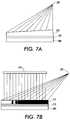
- Fig. 1shows an exemplary view of a known embodiment of a spectrometer apparatus disposed to measure the intensity of light 11 produced by a source 10.
- Source 10outputs a beam of multi-colored light which is imaged by an imaging lens 20 onto entrance slits 30 of a spectrometer 40.
- the slits 30are used to define the input trajectory of the light upon the optical elements of the spectrometer 40.
- the intensity of the lightis measured by a photosensitive detector 50, for example, at an exit aperture of the spectrometer 40.
- Fig. 2shows the internal and external components of the spectrometer apparatus of Fig. 1 in further detail.
- the slits 30admit the beam of light 11 containing at least two wavelength components, ⁇ 1 and ⁇ 2. For clarity, only the central ray of the beam of light 11 and no optical components within the spectrometer are shown in Fig. 2 .
- the beam of light 11is incident upon a wavelength dispersive means 35, shown in Fig. 2 as a grating, which reflects the light with a different phase angle, according to the portion of the grating that reflects the light.
- the light having a wavelength and phase anglesuch that the wavefronts constructively interfere at the detector, are measured by the detector 50 as having a given intensity. Therefore, the detector 50 may record the intensity as a function of wavelength, thereby producing the spectrum of the source 10.
- the photosensitive detector 50may have a plurality of discrete photosensitive elements, such as a detector array or charge-coupled device (CCD) array. Each photosensitive element may be independently accessible by a data collection apparatus, such as a computer.
- a data collection apparatussuch as a computer.
- Fig. 2shows the wavelength dispersive means as being a reflective grating
- other wavelength dispersive meansmay also be used in the spectrometer to separate the components of light according to wavelength.
- a prismwill refract the various components at a different angle depending on the wavelengths of the components.
- all spectrometersmust have some significant distance between the wavelength dispersive means 35 and the optical detector 50, in order to give the components a measurable separation.
- Fabry-Perot etalonAnother device which can separate wavelength components from a multi-colored light is a Fabry-Perot etalon.
- An exemplary Fabry-Perot etalonis shown in Fig. 3 .
- the Fabry-Perot etalon 70is composed of two reflective films 72 and 76, which are applied to the front and rear surfaces of a transmissive cavity 74.
- Light incident on the Fabry-Perot etalon 70will be transmitted if its wavelength is such that an integer number of half-wavelengths can be fit inside the thickness d of the transmissive cavity 74. In this case, light having this wavelength will be transmitted, whereas light of other wavelengths will be reflected.
- the reflectivity spectrum of the Fabry-Perot etalon 70is shown in Fig. 4 .
- a dip 78 in the reflectivity spectrumoccurs at the transmission wavelength of the Fabry-Perot etalon 70.
- Fabry-Perot etalonsare not, in general, used in spectrometers or wavelength shift detectors, because they are not tunable, and thus cannot produce a spectrum, or measure different wavelengths.
- WO-A-95/20144illustrates a device similar to that of Fig. 3 but using a wedge-shaped Fabry-Perot etalon and a CCD array detector.
- the requirement for a distance between the wavelength dispersive means 35 and the optical detector 50requires a spectrometer to be a relatively large, bulky device. The distance then also requires the spectrometer to undergo frequent alignment and calibration to adjust the angle of the grating or prism relative to the slits and detector, in orderto optimize performance. Furthermore, the distance between the optical elements and the detector in a conventional spectrometer makes the spectrometer sensitive to vibrations, so that it must be used in a stable, well-controlled environment.
- Gatdescribes a spectrum resolving sensor containing an opto-electronic monolithic array of photosensitive elements, and a linearly variable optical filter that is permanently aligned with the array.
- the linear variable filteris a substrate covered with variable thickness coatings formed into a wedge shape.
- the device described in Gatsuffers from using relatively expensive components, and having rather poor wavelength discrimination capabilities.
- US-A-2001/0007501describes an integrated wavelength monitor in which an interference filter is created directly on a position-sensitive photodetector. In use, the assembly is positioned at a required angle such that only light incident at a specific angle will be transmitted through the filter and be detected.
- US-A-5784507describes a spectrometer having a wedge-shaped wavelength discriminator so that light at different wavelengths passes through the discriminator at different lateral positions.
- This inventionprovides a method for measuring a wavelength shift according to claim 1.
- the output of the position-sensitive detectormay be two currents, whose normalized difference is proportional to the location of the light spot on the detector.
- the wavelength detectormay be used to measure the wavelength of a monochromatic source or to determine precisely a wavelength shift of the source.
- the position-sensitive photodetectormay be based on a continuous, homogeneous, non-discrete photosensitive medium, as distinct from an array of discrete photosensitive elements. Such detectors are far less expensive than detectors made from arrays of photosensitive elements. This is particularly true for any wavelength range where Si-based devices cannot be used. In addition, they have inherently better position resolution than arrays, for which the position resolution is limited by the size of the discrete photosensitive elements making up the array. The resolution of a position-sensitive detector is only limited by the accuracy with which a differential current can be measured. The typical resolution of position-sensitive detectors is less than 0.1 ⁇ m.
- Exemplary embodiments of a coating with laterally varying transmission propertiesmay be a Fabry-Perot cavity with a laterally varying thickness (e.g., a wedge-shaped etalon) or a cavity with laterally varying index of refraction.
- the wedge-shaped etalonhas a wedge-shaped transmissive cavity, having a thickness that varies across the surface of the detector and being positioned adjacent to at least one reflective layer.
- the wedge-shaped etalonhas a transmission function that varies across the surface of the detector according to the thickness of the transmissive cavity. Therefore, a shift in the wavelength of the input light causes a shift in the position of the transmitted spot on the photosensitive detector.
- Use of a wedge-shaped etalonsubstantially improves the wavelength selectivity over a linear variable filter, such as described in Gat.
- the reflective layers on the transmissive cavitymay be a plurality of thin films, with thicknesses and indices of refraction that are chosen to form a distributed Bragg reflector (DBR).
- DBRdistributed Bragg reflector
- the dielectric Fabry-Perot cavity with varying index of refractionmay be a film of material having uniform thickness, but varying material composition across the lateral dimension of the film. This can be, for instance, a Fabry-Perot cavity comprising a uniformly thick AlGaAs film with laterally varying Al content.
- Various examples and embodiments of the inventioncan be used to measure the wavelength or the wavelength shift of a single frequency light source.
- a first signal indicative of a location of a first detected spot of light at a first wavelengthis measured, and compared to a second signal indicative of a location of a second detected spot of light at a shifted wavelength, thereby producing a measurement of the wavelength shift between the two signals from the light source.
- the wavelength shiftcan be determined by a differential analog output signal which is proportional to the wavelength shift, and independent of light intensity.
- the position-sensitive detector 300may be a device which outputs a signal (e.g., a normalized current difference) which is proportional to the location of a light spot on the surface of the detector. For example, the position-sensitive detector 300 will output a different signal level, depending on whether a light spot falls on location #8 or location #9 on the position-sensitive detector 300.
- a signale.g., a normalized current difference
- the film assembly with laterally varying transmission propertiesmay be variable thickness etalon 100, which includes at least three sub-components, a wedge-shaped transmissive cavity 102, and two reflective films 101 and 103. Therefore, the three films 101, 102 and 103 form a wedge-shaped Fabry-Perot etalon.
- the wedge-shaped transmissive cavity 102has a thickness d which varies as a function of the distance x along the lateral dimension of the wedge. Therefore, the wedge-shaped etalon 100 will transmit different wavelengths ⁇ as a function of lateral distance x.
- variable thickness etalon 100comprising the wedge-shaped transmissive cavity 102 and the two reflecting films 101 and 103, shown in Fig. 5 may be disposed adjacent to a position-sensitive detector 300.
- a source 10may output, at different times, light of wavelength ⁇ and wavelength-shifted light of wavelength A + ⁇ .
- light source 10outputs light of wavelength ⁇ , at a certain location in the wedged etalon 100, the wavelength ⁇ is transmitted through the etalon 100, and impinges upon a location, for example, location indicated by #8, on the position-sensitive detector 300.
- the wavelength-shifted light ⁇ + ⁇is reflected from the etalon 100 at the position corresponding to location #8.
- the wavelength-shifted light ⁇ + ⁇is transmitted through the etalon 100, whereas wavelength A is reflected. Therefore, the output of the position-sensitive detector will correspond to the illumination of location #8 when light comprising wavelength A is incident on the chip-size wavelength detector 1000.
- the position-sensitive detector 300will output a signal corresponding to the illumination of location #9.
- Fig. 6shows an exemplary ideal reflectivity spectrum for the variable thickness etalon 100 of Fig. 5 .
- all wavelengths except for the transmission wavelengthare reflected with nearly 100% efficiency, whereas wavelengths at or near the transmission wavelength are transmitted with an efficiency of nearly 100%.
- the reflectivity of the variable thickness etalon 100is nearly zero, such that nearly 100% of the light intensity at A is transmitted through the variable thickness etalon 100.
- the reflectivity for light at a wavelength of about 810 nm ( ⁇ + ⁇ )is nearly 100%, such that essentially all of the light at ⁇ is transmitted, whereas virtually all of the light at ⁇ + ⁇ is reflected.
- the film 100transmits nearly all of the light at 810 nm ( ⁇ + ⁇ ) and reflects nearly all of the light at the wavelength of A. Therefore, obtaining a signal from position-sensitive detector proportional to position #8 indicates the presence of light having a wavelength of ⁇ , obtaining a signal from the position-sensitive detector proportional to position #9 indicates the presence of light having a wavelength of ⁇ + ⁇ . Measuring the displacement between location #9 and location #8, gives a measure of the wavelength shift ⁇ according to a previously obtained calibration curve, as described further below.
- Fig. 7ashows a schematic diagram of a manufacturing setup which can be used to produce the wedged transmissive cavity 102 of wedged etalon 100 of Fig. 5 .
- the wedged transmissive cavity 102 and reflectors 101 and 103are deposited directly over the surface of the position-sensitive detector 300, using the position-sensitive detector 300 as a substrate.
- the wedged transmissive cavity and lower and upper reflectors 101 and 103may be deposited on a transparent substrate, which is subsequently assembled onto the position-sensitive detector 300.
- the thickness of the wedged transmissive cavity 102may be made variable, by displacing the position-sensitive detector 300 away from the location which would correspond to the symmetric, shortest distance between the position-sensitive detector 300 and a source 500 of the deposition species. (The symmetric, shortest distance position would have the source 500 placed midway between the ends of the position-sensitive detector 300, and with the position-sensitive detector 300 oriented in a plane normal to the direction of the source 500 from the position-sensitive detector 300.) An exemplary orientation of the position-sensitive detector 300 with respect to the source 500 is shown in Fig. 7a .
- the position-sensitive detector 300Since the portion of the position-sensitive detector 300 which is closer to the source 500 intercepts a larger flux of the deposited species, it forms a thicker film over these regions than the region located further away from the source 500. In a molecular beam epitaxy (MBE) system, this configuration can easily be achieved by stopping the wafer rotation during the growth of the cavity.
- MBEmolecular beam epitaxy
- the position-sensitive detector 300may also be placed at an angle relative to the normal trajectory of the deposited species on the position-sensitive detector 300. For either example, the angle or the placement of the photosensitive detector is chosen to form a wedge of the appropriate angle. In the exemplary embodiments described below, the angle of the wedge was less than 10 -4 °.
- this wavelength shiftwas about 30 nm per cm, which corresponds to a wedge angle of about 2 x 10 -4 °.
- This Fabry-Perot coating with wedged GaAs cavitywas fabricated with a conventional molecular beam epitaxy system by simply stopping the substrate rotation during growth of the cavity.
- the location (angle with regard to normal incidence and/or of center displacement) for placing the substratecan be chosen within a wide range.
- the proper angle for deposition of the materialmay be determined experimentally, by depositing the wedged film and thereafter measuring its transmission properties.
- variable thickness optical film 100Other methods may also be used to fabricate the variable thickness optical film 100, such as using a shadow mask or a temperature gradient to vary the deposition rate of the wedged film 102 over the surface of the position-sensitive detector 300.
- Fig. 5is an etalon with constant thickness but laterally varying refractive index.
- Fig. 7bshows a schematic diagram of the fabrication setup which can be used to produce such an etalon. In this setup, a source of alloy or dopant material 520 is disposed offset from the symmetric, shortest distance position to the position-sensitive detector 300, while a source of the deposited material 510 is disposed symmetrically above the position-sensitive detector 300.
- the alloy or dopant source 520changes the material composition of the uniformly thick film 112 laterally across the film 112.
- the source of deposited material 510may be GaAs or glass, and the alloy or dopant source may be Al or Ge.
- the choice of materials and the transmission properties of the filmwill depend on the application.
- Fig. 7cshows a measurement of the transmission properties of a AlGaAs/GaAs Fabry-Perot structure made by molecular beam epitaxy, in a manufacturing setup similar to that shown in Fig. 7a .
- the transmission of the filmis a function of wavelength, and shows a distinct peak at a certain wavelength, for each position along the film.
- Fig. 7cshows the transmission characteristics for eleven such positions across the film.
- the peak of the transmitted wavelengthchanges from 932.5 nm to 967.5 nm, between position 1 and position 11.
- the distance between position 1 and position 11is about 500 mils, so that the calibration for this device is about 0.07 nm per mil or about 3 nm per mm. Therefore, a wavelength shift of 0.01 nm is easily detectable on this device, as a lateral shift of the spot on the detector of about 3 ⁇ m.
- the resolving power, also known as the finesse, of the etalon 100may depend, in part, on the reflectivities of the front and rear surfaces 101 and 103.
- the finesse of the etalonmay be increased, thereby narrowing the full width half maximum of the reflectivity dip in the etalon.
- the films 101 and 103may be constructed using highly reflective distributed Bragg reflectors.
- Distributed Bragg reflectorsmay be selected because the reflectivities of such multilayer films can be made almost arbitrarily high, depending on the number of pairs of films and the differences in their refractive indices.
- the dielectric layersIn order to achieve high reflectivities, the dielectric layers must have high purity (few defects) to prevent absorption, the thickness of the layers should be precisely controlled, and the interface between materials should be smooth to prevent light scattering.
- Vacuum film deposition techniquessuch as thermal evaporation or electron beam evaporation are usually used in industrial applications to achieve highly reflective distributed Bragg reflectors.
- the wedge-shaped etalon 120comprises a wedge-shaped transmissive cavity 122, and two reflectors 121 and 123.
- the reflectors 121 and 123are themselves multi-layer films, wherein the individual layers of the reflectors 121 and 123 are selected or formed with a thickness and an index of refraction to constitute a distributed Bragg reflector (DBR), as described above.
- DBRdistributed Bragg reflector
- the two reflectors 121 and 123may be deposited with the wedge-shaped transmissive cavity 122, directly onto photosensitive detector 300.
- the two reflectors 121 and 123 and the wedge-shaped transmissive cavity 122may be deposited on thin substrates and assembled together with the photosensitive detector 300 after formation.
- the materials making up the distributed Bragg reflector films 121 and 123may be alternating layers of gallium arsenide (GaAs) and aluminum arsenide (AlAs).
- GaAsgallium arsenide
- AlAsaluminum arsenide
- the following filmsmay be deposited by molecular beam epitaxy (MBE) on a GaAs substrate with the following thicknesses: Table 1 Anti-Reflection Coating SiO 2 120nm Top DBR mirror 15 pairs of undoped GaAs/AIAs mirrors (GaAs on top) GaAs: 67.0 nm AlAs: 80.4 nm Graded cavity Undoped GaAs. Graded due to intrinsic thickness variation during growth.
- GaAs268 nm
- Other alternative material deposition processesinclude metal organic chemical vapor deposition (MOCVD), electron-beam evaporation, and sputtering.
- Table 1Materials Refractive index @ 950 nm Transparency Range Manufacturing technique, e.g.
- Table 3Materials Difference of refractive index @ 950 nm Mirror pairs within a DBR mirror Maximum Side band suppression FWHM of transmission peak GaAs/AlAs 18% 5 10 -2 8.8 nm GaAs/AlAs 18% 10 10 -3 1.2 nm SiO 2 /TiO 2 56% 5 10 -4 1.7 nm SiO 2 /TiO 2 56% 10 10 -8 0.01 nm
- the wedge-shaped etalon 120 shown schematically in Fig. 8was fabricated according to the above parameters in Table 1 using about 15 pairs of alternating GaAs and AlAs to form the films 121 and 123, and a wedge-shaped transmissive cavity 122 of undoped GaAs, nominally about 270 nm thick.
- Each GaAs layer of the DBR structures 121 and 123is about 67 nm thick, with a refractive index of about 3.55
- each AlAs layer of the DBR structures 121 and 123is about 80.4 nm thick with a refractive index of about 2.95. Therefore, based on equations (1) and (2), the transmission window of the wedge-shaped etalon was designed to be about 950 nm.
- the wedge angle ⁇ of the wedge-shaped transmissive cavity 122is determined based on the desired spectral range of the wedge-shaped etalon 120.
- the ideal transmission spectrum of the wedge-shaped etalon 120 with distributed Bragg reflectors 121 and 123, such as was shown in Fig. 8is shown in Fig. 9 .
- the data in Fig. 9show calculated results for various points 1-9 along the wedge-shaped etalon 120.
- the overall full width half maximum of the transmission dipsis about 1 nm, and the nominal reflectivity of the wedge-shaped etalon 120 is 99.8%.
- the resolution of the systemdepends strongly on resolution capability of the position-sensitive detector 300, the full width half maximum of the transmission dip, and on the peak shift per unit displacement of the wedge-shaped etalon 120. The smaller the full width half maximum and the peak shift, the better the resolution. However, the larger the full width half maximum and peak shift per unit displacement, the larger the spectral range which can be covered by the chip-size wavelength detector 1200.
- the wedge-shaped etalon 120 producing the reflectivity curve shown in Fig. 9spans a position-sensitive detector which is about 10 mm across. Based on these dimensions, the total spectral range shown in Fig. 9 of about 60 nm, and on equation (1) and the parameters given in Table 2 above, the wedge-shaped transmissive cavity 122 has a wedge angle ⁇ of less than about 0.0001 degrees, and a corresponding wavelength shift versus displacement of about 6 nm/mm. Such small wedge angles and even much smaller angles can be easily achieved with thin-film deposition techniques, such as molecular beam epitaxy (MBE).
- MBEmolecular beam epitaxy
- Fig. 10shows an exemplary embodiment of a position-sensitive detector 300 that may be used in the wavelength shift detector 1200.
- a three-terminal semiconductor deviceis used to generate a signal which is proportional to the location of a light spot falling on the detector surface.
- the detector surfacemay be located between two output electrodes, and the differential current flowing from a bias electrode to each of the output electrodes may correspond to the position of the light spot on the sensor.
- a position sensor of this typeis the 1L10 manufactured by On-Trak Photonics, Inc. of Lake Forest, California.
- the position-sensitive detector 300comprises an n-type silicon substrate 331 with two resistive layers separated by a p-n junction.
- the front sidehas an ion implanted p-type resistive layer 335 with two contacts or electrodes 332 and 334 at opposite ends.
- the back sidehas an ion implanted n-type resistive layer 336 which serves as the bias electrode 333 for the device.
- the electrodes 332 and 334are placed at opposite ends of the p-type resistive layer 335.
- a light spot within the spectral range of siliconwill generate a photocurrent which flows from an incident point 338 through the resistive layers 335 and 336 to the electrodes 332 and 334.
- the resistivity of the p-type resistive layer 335is extremely uniform so the photocurrent generated at each electrode 332 and 334 is inversely proportional to the distance between the incident point 338 and the electrodes 332 and 334.
- the position-sensitive detector 300may be 10 mm long, and may have a position sensitivity of better than about 0.1 ⁇ m.
- a five-terminal position-sensitive detectormay be used, which can locate the position of the spot falling on the detector surface in two dimensions.
- the detector surfacecan be located between the two pairs of electrodes on the front side of the position-sensitive detector and a single bias electrode on the back side.
- This position-sensitive detectormay be used with a laterally varying transmissive film, wherein the film varies laterally in the two dimensions, for example, with a relatively steep gradient in one dimension and a shallower gradient in the other.
- the position-sensitive detector 300can be fabricated in an integrated circuit-type housing, which provides electrical connections via output pins to position-sensitive detector 300.
- the output pinscan then be coupled electrically to a cable or wire, such that signals outputted by the position-sensitive detector 300 can be acquired by a data collection apparatus such as a computer.
- the differential read-out of the two currents of the position sensorcan be achieved either by an integrated internal or external electronic circuit (e.g., an operational amplifier) or by a computer. Since such techniques are well known in the art, they are not depicted in Fig. 10 , or described further herein.
- Fig. 11shows a third exemplary embodiment of a chip-size wavelength detector 1200 using the position sensor 300 of Fig. 10.
- Fig. 11shows a wedge-shaped etalon 120 applied to the surface of the position-sensitive detector 300.
- the wedge-shaped etalon 120is a distributed Bragg reflector/etalon stack similar to that shown in Fig. 8 .
- the distributed Bragg reflector layerswere composed of alternating layers of AlAs and GaAs, with a GaAs cavity, all deposited by molecular beam epitaxy. Because the peak transmission for a given wavelength will depend upon the width of the transmissive cavity 122 of the wedged Fabry-Perot etalon 120, the position of the maximum transmitted intensity will shift along the position-sensitive detector 300, as a function of wavelength.
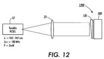
- Fig. 12shows an arrangement which can be used to calibrate or test a chip-size wavelength detector 1200, or to measure the wavelength of a single frequency source.
- the chip-size wavelength detector 1200 shown in Fig. 8may be illuminated by a collimated, single-frequency laser source 12, as shown in Fig. 12 .
- the single frequency laser source 12may be a semiconductor vertical cavity surface emitting laser (VCSEL), which is tunable between about 942 nm and 947 nm, by adjusting the operating temperature of the semiconductor device.
- the linewidth of the single frequency laser source 12is about 100 MHz, and the output power is about 2 mW.
- the output of the single-frequency laser source 12is collimated by a collimating lens 23.
- the wedge-shaped etalon 120is shown schematically only as the wedge-shaped element 120, however it should be clear that the other components of the wedge-shaped etalon 120 shown in greater detail in Fig. 8 are also present.
- the setup shown in Fig. 12is described in terms of a calibration operation, it should be clear to one skilled in the art that the exact same setup can be used to measure the wavelength generated by the source 12.
- the wedged etalon 120may be fabricated directly on a detector mounted in an integrated circuit-type housing, it is straightforward to integrate these devices into more complex electronic detection systems.
- the chip-size wavelength detector 1200may easily allow the creation of an interactive detection system, wherein the results of the spectral analysis is used to then alter the properties or performance of the source 12. Also, subsequent or adjacent position-sensitive detectors may trigger other events occurring within the detection system.
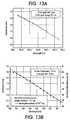
- Fig. 13ashows the differential output of electrode 334 as compared to electrode 332 (see Fig. 11 ), normalized by the sum of the currents, for the chip-size wavelength detector 1200.
- the differential output signalcan be defined as: I L ⁇ I R / I L + I R where I L is the current flowing between electrode 334 and electrode 333, and I R is the current flowing between electrode 332 and electrode 333.
- the differential outputis shown to be approximately linear throughout the range from about 942.75 nm to about 945.25 nm.
- the total wavelength range measuredwas 2.5 nm, spanning a detector surface length of 0.76 mm, such that a 3.3 nm shift in the peak wavelength caused a shift in the location of the detected spot 338 by about 1 mm.
- the position sensitivity of the position-sensitive detector 300is better than about 0.1 ⁇ m, the sensitivity of this wavelength detector 1200 to wavelength shifts is about 0.33 x 10 -3 nm.
- the relationship between displacement and wavelength, shown in Fig. 13aconstitutes the calibration curve for the chip-size wavelength detector 1200. Coatings or etalons with a peak wavelength shift of less than 1 nm can easily be fabricated. Therefore devices with an even better resolution ( ⁇ 10 -4 nm) are possible.
- Fig. 13bshows the relationship between displacement and wavelength for a halogen lamp spectrally filtered by a monochromator. Because the monochromator is more widely tunable than the VCSEL, the relationship between displacement and wavelength is shown to be linear over a wider range. This suggests that high resolution measurements as described above can be performed over a very broad spectral range.
- the wavelength detector 1200may also be capable of generating spectra of multi-colored sources such as plasmas, filtered through a monochromator.
- the position-sensitive detector 300is capable of measuring shifts in the position of the light spot to less than about 0.1 ⁇ m, it is capable of measuring wavelength shifts in the range of less than about 1 x 10 -4 nm, despite using very simple and inexpensive technology. Being relatively independent of light intensity also relieves this embodiment of the requirement of careful gain calibration of the detector response, although each chip-size wavelength detector 1200 will still, in general, need to be wavelength calibrated using a known light source, as discussed above. Note that the precise determination of a wavelength shift is possible even without accurate calibration.
- a calibration curvesuch as that shown in Fig. 13a and 13b , relates the displacement of the light spot on the position-sensitive detector to a wavelength shift of the incoming light.
- the calibration curveis primarily associated with the details of the films comprising the wedge-shaped etalon 120 on detector 300 of the chip-size wavelength detector 1200.
- the wedge-shaped etalon 120is rigidly adhered to the detector 300, and cannot, in general, be dislodged by vibration or impact. Therefore, unlike full-size grating-based or prism-based spectrometers such as that shown in Figs.
- the calibration curveis not expected to change with external conditions such as the orientation of the chip-size wavelength detector 1200, shock or vibration, and need not be repeated unless an event occurs which changes the physical condition of the wedge-shaped etalon 120, such as extreme temperatures.
- the wavelength detectormay be capable of measuring absolute wavelengths, as well as wavelength shifts, to high accuracy.
- the calibration of the device in terms of absolute wavelength measurementmay be affected by changes in temperature.
- a temperature sensormay be integrated with the wavelength detector 1200, allowing the wavelength detector 1200 to be calibrated for a number of temperatures. Calibrations as a function of temperature may then be stored as a lookup table, to correct the output of the wavelength detector for any of a number of different operating temperatures.
- the chip-size wavelength detectormay be temperature-stabilized, for example using a thermoelectric cooler such as those used to stabilize the output of diode lasers.
- the chip-size wavelength detector 1200may be deployed in any range of operating environments, without needing to recalibrate the device.
- the chip-size wavelength detectorwould be expected to perform similarly whether in an evacuated environment such as outer space, as in an environment with a different ambient index of refraction, such as submerged underwater.
- the response of the chip-size wavelength shift detectorwould not be expected to change, unlike conventional spectrometers, which rely on refracting prisms or diffraction gratings, which inherently depend on the index of refraction of the medium in which they are operating.
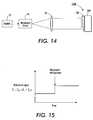
- the chip-size wavelength detector 1200can be used, for example, to measure an unknown wavelength shift.
- a single frequency source 13is transmitted through a wavelength shifting mechanism 14, which shifts the wavelength of the light by some unknown amount.
- a wavelength shifting mechanismis the shifting of the wavelength of a laser as a result of temperature or changes in the dimensions of a laser cavity.
- the chip-size wavelength detector 1200is disposed to measure the wavelength of the single frequency source 13, before and after the wavelength shift mechanism is switched on and off.
- Fig. 15shows schematically the results of measuring the effects of imposing a wavelength shift event, such as, for example, changing the output of a thermoelectric cooler implemented to tune the frequency of a single-mode semiconductor laser.
- a wavelength shift eventsuch as, for example, changing the output of a thermoelectric cooler implemented to tune the frequency of a single-mode semiconductor laser.
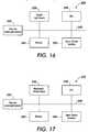
- Fig. 16shows a system 3000 capable of calibrating a chip-size wavelength detector 3300, such as those shown in Figs. 5 , 8 , or 11 .
- the system 3000may include a CPU 3100, a tunable light source 3210, a chip-size wavelength detector 3300, a memory 3400, and an input/output interface 3500.
- the above componentsmay be coupled together, for example, via a bus 3600.
- the measurement system 3000is illustrated using a bus architecture diagram, any other type of hardware and/or software configuration may be used.
- ASICsapplication specific integrated circuits
- ASICsapplication specific integrated circuits
- the tunable light source 3210may have its output tuned by the CPU 3100, while the CPU 3100 also acquires data from the chip-size wavelength detector 3300.
- the datais acquired by taking the differential signal from the position sensor 300 of the chip-size wavelength detector 3300.
- the CPU 3100stores the acquired data in memory 3400.
- the CPUcan measure the relationship between displacement on the position-sensitive detector 300 and wavelength, and store this relationship in memory 3400.
- the CPUcan measure a gain coefficient for the position-sensitive detector, and store the gain coefficient also in memory 3400. This gain coefficient may be used to calibrate the output of the position-sensitive detector, in the event that an intensity measurement is made, as described above, by calculating the sum of the currents I R and I L .
- the tunable light source 3210may be substituted with a wavelength-shifted light source 3700, in the experimental arrangement 3150 shown in Fig. 17 , to perform the measurement step.
- the CPU 3100queries the wavelength detector 3300 for the position of the unshifted light spot on the wavelength detector 3300.
- the CPUstores this value in memory 3400.
- the wavelength shifting mechanismis then applied to the wavelength-shifted light source 3700, and the CPU again queries the chip-size wavelength detector 3300 for the position of the shifted light spot.
- the CPUcompares the position of the unshifted light spot with the wavelength-shifted light spot, to determine a displacement between the light spots. Then, using the stored relationship between displacement and wavelength, the wavelength shift of the wavelength-shifted source may be determined.
Landscapes
- Physics & Mathematics (AREA)
- Spectroscopy & Molecular Physics (AREA)
- General Physics & Mathematics (AREA)
- Spectrometry And Color Measurement (AREA)
- Photometry And Measurement Of Optical Pulse Characteristics (AREA)
- Investigating Or Analysing Materials By Optical Means (AREA)
Description
- This invention is directed to a method for measuring a wavelength shift.
- Spectrometers and wavelength shift detectors are widely used in scientific, academic and industrial applications to measure the various wavelengths of multi-colored light. Known spectrometers use a wavelength dispersive means, such as a prism or grating, to separate components of the multi-colored light according to the wavelengths of the components. The intensity of the wavelength components is then measured by a photodetector.
- Wavelength shift detectors may also use wavelength dispersive means. However, instead of measuring intensity as a function of wavelength, they generally measure a shift in wavelength of a single frequency source away from a nominal value. Often spectrometers are used to measure the wavelength shift, however the wavelength resolution is typically poor, on the
order 10-2 nm. For applications where high wavelength resolution is needed, a Mach-Zehnder type wavelength meter is sometimes used. Fig. 1 shows an exemplary view of a known embodiment of a spectrometer apparatus disposed to measure the intensity oflight 11 produced by asource 10.Source 10 outputs a beam of multi-colored light which is imaged by animaging lens 20 ontoentrance slits 30 of aspectrometer 40. Theslits 30 are used to define the input trajectory of the light upon the optical elements of thespectrometer 40. The intensity of the light is measured by aphotosensitive detector 50, for example, at an exit aperture of thespectrometer 40.Fig. 2 shows the internal and external components of the spectrometer apparatus ofFig. 1 in further detail. Theslits 30 admit the beam oflight 11 containing at least two wavelength components, λ1 and λ2. For clarity, only the central ray of the beam oflight 11 and no optical components within the spectrometer are shown inFig. 2 . The beam oflight 11 is incident upon a wavelength dispersive means 35, shown inFig. 2 as a grating, which reflects the light with a different phase angle, according to the portion of the grating that reflects the light. The light having a wavelength and phase angle such that the wavefronts constructively interfere at the detector, are measured by thedetector 50 as having a given intensity. Therefore, thedetector 50 may record the intensity as a function of wavelength, thereby producing the spectrum of thesource 10.- According to
Fig. 2 , thephotosensitive detector 50 may have a plurality of discrete photosensitive elements, such as a detector array or charge-coupled device (CCD) array. Each photosensitive element may be independently accessible by a data collection apparatus, such as a computer. - While
Fig. 2 shows the wavelength dispersive means as being a reflective grating, one skilled in the art will understand that other wavelength dispersive means may also be used in the spectrometer to separate the components of light according to wavelength. For example, a prism will refract the various components at a different angle depending on the wavelengths of the components. However, regardless of the means used to disperse the wavelength components of the multi-colored light, it will be appreciated that all spectrometers must have some significant distance between the wavelengthdispersive means 35 and theoptical detector 50, in order to give the components a measurable separation. - Another device which can separate wavelength components from a multi-colored light is a Fabry-Perot etalon. An exemplary Fabry-Perot etalon is shown in
Fig. 3 . The Fabry-Perotetalon 70 is composed of tworeflective films transmissive cavity 74. Light incident on the Fabry-Perotetalon 70 will be transmitted if its wavelength is such that an integer number of half-wavelengths can be fit inside the thickness d of thetransmissive cavity 74. In this case, light having this wavelength will be transmitted, whereas light of other wavelengths will be reflected. The reflectivity spectrum of the Fabry-Perotetalon 70 is shown inFig. 4 . Adip 78 in the reflectivity spectrum occurs at the transmission wavelength of the Fabry-Perotetalon 70. Fabry-Perot etalons are not, in general, used in spectrometers or wavelength shift detectors, because they are not tunable, and thus cannot produce a spectrum, or measure different wavelengths. WO-A-95/20144 Fig. 3 but using a wedge-shaped Fabry-Perot etalon and a CCD array detector.- The requirement for a distance between the wavelength dispersive means 35 and the
optical detector 50 requires a spectrometer to be a relatively large, bulky device. The distance then also requires the spectrometer to undergo frequent alignment and calibration to adjust the angle of the grating or prism relative to the slits and detector, in orderto optimize performance. Furthermore, the distance between the optical elements and the detector in a conventional spectrometer makes the spectrometer sensitive to vibrations, so that it must be used in a stable, well-controlled environment. - One approach to making a spectrometer which does not need to be aligned, and is compact and robust, is disclosed in
U.S. Patent 5,166,755 to Gat. Gat describes a spectrum resolving sensor containing an opto-electronic monolithic array of photosensitive elements, and a linearly variable optical filter that is permanently aligned with the array. The linear variable filter is a substrate covered with variable thickness coatings formed into a wedge shape. - However, the device described in Gat suffers from using relatively expensive components, and having rather poor wavelength discrimination capabilities.
US-A-2001/0007501 describes an integrated wavelength monitor in which an interference filter is created directly on a position-sensitive photodetector. In use, the assembly is positioned at a required angle such that only light incident at a specific angle will be transmitted through the filter and be detected.US-A-5784507 describes a spectrometer having a wedge-shaped wavelength discriminator so that light at different wavelengths passes through the discriminator at different lateral positions.- This invention provides a method for measuring a wavelength shift according to
claim 1. The output of the position-sensitive detector may be two currents, whose normalized difference is proportional to the location of the light spot on the detector. The wavelength detector may be used to measure the wavelength of a monochromatic source or to determine precisely a wavelength shift of the source. - The position-sensitive photodetector may be based on a continuous, homogeneous, non-discrete photosensitive medium, as distinct from an array of discrete photosensitive elements. Such detectors are far less expensive than detectors made from arrays of photosensitive elements. This is particularly true for any wavelength range where Si-based devices cannot be used. In addition, they have inherently better position resolution than arrays, for which the position resolution is limited by the size of the discrete photosensitive elements making up the array. The resolution of a position-sensitive detector is only limited by the accuracy with which a differential current can be measured. The typical resolution of position-sensitive detectors is less than 0.1 µm.
- Exemplary embodiments of a coating with laterally varying transmission properties may be a Fabry-Perot cavity with a laterally varying thickness (e.g., a wedge-shaped etalon) or a cavity with laterally varying index of refraction. The wedge-shaped etalon has a wedge-shaped transmissive cavity, having a thickness that varies across the surface of the detector and being positioned adjacent to at least one reflective layer. The wedge-shaped etalon has a transmission function that varies across the surface of the detector according to the thickness of the transmissive cavity. Therefore, a shift in the wavelength of the input light causes a shift in the position of the transmitted spot on the photosensitive detector. Use of a wedge-shaped etalon substantially improves the wavelength selectivity over a linear variable filter, such as described in Gat.
- The reflective layers on the transmissive cavity may be a plurality of thin films, with thicknesses and indices of refraction that are chosen to form a distributed Bragg reflector (DBR). Using highly reflective Bragg reflectors further improves the wavelength selectivity of the wedge-shaped etalon.
- The dielectric Fabry-Perot cavity with varying index of refraction may be a film of material having uniform thickness, but varying material composition across the lateral dimension of the film. This can be, for instance, a Fabry-Perot cavity comprising a uniformly thick AlGaAs film with laterally varying Al content.
- Various examples and embodiments of the invention can be used to measure the wavelength or the wavelength shift of a single frequency light source. To measure a wavelength shift, a first signal indicative of a location of a first detected spot of light at a first wavelength is measured, and compared to a second signal indicative of a location of a second detected spot of light at a shifted wavelength, thereby producing a measurement of the wavelength shift between the two signals from the light source. The wavelength shift can be determined by a differential analog output signal which is proportional to the wavelength shift, and independent of light intensity.
- These and other features and advantages of this invention are described in, or are apparent from, the following detailed description of various exemplary embodiments of the systems and methods according to this invention.
Fig. 1 is a schematic diagram of a known spectrometer apparatus;Fig. 2 is a schematic diagram of the elements of the known spectrometer apparatus ofFig. 1 ;Fig. 3 is a diagram of a known Fabry-Perot etalon;Fig. 4 is a reflectivity spectrum of the Fabry-Perot etalon ofFig. 3 ;Fig. 5 is a diagram of a first exemplary embodiment of a chip-size wavelength detector which can be used to measure the wavelength shift according to this invention;Fig. 6 is a schematic plot of the reflectivity spectrum of the wedge-shaped etalon ofFig. 5 ;Fig. 7a is a schematic diagram illustrating a manufacturing method for making the wavelength detector ofFig. 5 .Fig. 7b is a schematic diagram illustrating a manufacturing method for making a wavelength detector with a laterally varying index of refraction.Fig. 7c is a measurement of the transmission properties of the Fabry-Perot cavity made by the setup ofFig. 7a , as a function of lateral position across the film;Fig. 8 is a schematic diagram of a second exemplary embodiment of a chip-size wavelength detector which can be used to measure the wavelength shift according to this invention;Fig. 9 is a schematic reflectivity spectrum of the dielectric Fabry-Perot structure with wedge-shaped cavity shown inFig. 8 ;Fig. 10 shows an exemplary embodiment of a position sensor, usable in this invention;Fig. 11 shows the position sensor ofFig. 10 used in a third exemplary embodiment of a chip-size wavelength detector which can be used to measure the wavelength shift according to this invention;Fig. 12 is a schematic diagram of a setup for calibrating a chip-size wavelength detector and spectrometer ;Fig. 13a shows the displacement versus wavelength curve of the wavelength detector in response to the tuning of the single frequency VCSEL source.Fig. 13b shows the displacement versus wavelength curve of the wavelength detector in response to light from a halogen lamp spectrally filtered by a monochromator;Fig. 14 is a schematic diagram of an experimental setup using a chip-size wavelength detector according to this invention;Fig. 15 is a sample output of the wavelength detector in response to a wavelength-shifting event;Fig. 16 illustrates an exemplary calibration system using the exemplary chip-size wavelength detector; andFig. 17 illustrates an exemplary system for measuring the wavelength shift of a wavelength-shifted source using the exemplary chip-size wavelength detector.Fig. 5 shows a first exemplary embodiment of the chip-size wavelength detector 1000, according to this invention. As shown inFig. 5 , the chip-size wavelength detector 1000 includes two components, a film assembly with laterally varyingtransmission properties 100 and a position-sensitive detector 300. Thewavelength detector 1000 may be used to determine the absolute wavelength of a monochromatic source, or it may be used to measure a wavelength shift of a source away from a nominal wavelength.- The position-
sensitive detector 300 may be a device which outputs a signal (e.g., a normalized current difference) which is proportional to the location of a light spot on the surface of the detector. For example, the position-sensitive detector 300 will output a different signal level, depending on whether a light spot falls onlocation # 8 orlocation # 9 on the position-sensitive detector 300. - The film assembly with laterally varying transmission properties may be
variable thickness etalon 100, which includes at least three sub-components, a wedge-shapedtransmissive cavity 102, and tworeflective films films transmissive cavity 102 has a thickness d which varies as a function of the distance x along the lateral dimension of the wedge. Therefore, the wedge-shapedetalon 100 will transmit different wavelengths λ as a function of lateral distance x. In particular, the transmitted wavelength is
- The
variable thickness etalon 100 comprising the wedge-shapedtransmissive cavity 102 and the two reflectingfilms Fig. 5 may be disposed adjacent to a position-sensitive detector 300. Asource 10 may output, at different times, light of wavelength λ and wavelength-shifted light of wavelength A + Δλ. Whenlight source 10 outputs light of wavelength λ, at a certain location in the wedgedetalon 100, the wavelength λ is transmitted through theetalon 100, and impinges upon a location, for example, location indicated by #8, on the position-sensitive detector 300. If thelight source 10 outputs wavelength-shifted light of wavelength λ + Δλ, the wavelength-shifted light λ + Δλ is reflected from theetalon 100 at the position corresponding tolocation # 8. However, at another point corresponding to thelocation # 9, the wavelength-shifted light λ + Δλ is transmitted through theetalon 100, whereas wavelength A is reflected. Therefore, the output of the position-sensitive detector will correspond to the illumination oflocation # 8 when light comprising wavelength A is incident on the chip-size wavelength detector 1000. When light comprising a component having wavelength A + Δλ is incident on chip-size wavelength detector 1000, the position-sensitive detector 300 will output a signal corresponding to the illumination oflocation # 9. Fig. 6 shows an exemplary ideal reflectivity spectrum for thevariable thickness etalon 100 ofFig. 5 . According toFig. 6 , all wavelengths except for the transmission wavelength are reflected with nearly 100% efficiency, whereas wavelengths at or near the transmission wavelength are transmitted with an efficiency of nearly 100%. For example, as shown inFig. 6 , at a first position corresponding tolocation # 8 on thevariable thickness etalon 100, and at a first wavelength of about 800 nm, (A), the reflectivity of thevariable thickness etalon 100 is nearly zero, such that nearly 100% of the light intensity at A is transmitted through thevariable thickness etalon 100. However the reflectivity for light at a wavelength of about 810 nm (λ + Δλ) is nearly 100%, such that essentially all of the light at λ is transmitted, whereas virtually all of the light at λ + Δλ is reflected. However, at a second, adjacent position corresponding tolocation # 9 in theoptical film 100, thefilm 100 transmits nearly all of the light at 810 nm (λ + Δλ) and reflects nearly all of the light at the wavelength of A. Therefore, obtaining a signal from position-sensitive detector proportional toposition # 8 indicates the presence of light having a wavelength of λ, obtaining a signal from the position-sensitive detector proportional toposition # 9 indicates the presence of light having a wavelength of λ + Δλ. Measuring the displacement betweenlocation # 9 andlocation # 8, gives a measure of the wavelength shift Δλ according to a previously obtained calibration curve, as described further below.Fig. 7a shows a schematic diagram of a manufacturing setup which can be used to produce the wedgedtransmissive cavity 102 of wedgedetalon 100 ofFig. 5 . In this manufacturing setup, the wedgedtransmissive cavity 102 andreflectors sensitive detector 300, using the position-sensitive detector 300 as a substrate. Alternatively, the wedged transmissive cavity and lower andupper reflectors sensitive detector 300.- The thickness of the wedged
transmissive cavity 102 may be made variable, by displacing the position-sensitive detector 300 away from the location which would correspond to the symmetric, shortest distance between the position-sensitive detector 300 and asource 500 of the deposition species. (The symmetric, shortest distance position would have thesource 500 placed midway between the ends of the position-sensitive detector 300, and with the position-sensitive detector 300 oriented in a plane normal to the direction of thesource 500 from the position-sensitive detector 300.) An exemplary orientation of the position-sensitive detector 300 with respect to thesource 500 is shown inFig. 7a . - Since the portion of the position-
sensitive detector 300 which is closer to thesource 500 intercepts a larger flux of the deposited species, it forms a thicker film over these regions than the region located further away from thesource 500. In a molecular beam epitaxy (MBE) system, this configuration can easily be achieved by stopping the wafer rotation during the growth of the cavity. In an alternative example of the manufacturing setup usable for forming thetransmissive cavity 102, the position-sensitive detector 300 may also be placed at an angle relative to the normal trajectory of the deposited species on the position-sensitive detector 300. For either example, the angle or the placement of the photosensitive detector is chosen to form a wedge of the appropriate angle. In the exemplary embodiments described below, the angle of the wedge was less than 10-4°. - Since typical angles are so small it is more suitable to specify the resulting shift of the transmission wavelength for a given lateral movement across the film. For example, with respect to
Fig. 7c , described below, this wavelength shift was about 30 nm per cm, which corresponds to a wedge angle of about 2 x 10⁻⁴°. This Fabry-Perot coating with wedged GaAs cavity was fabricated with a conventional molecular beam epitaxy system by simply stopping the substrate rotation during growth of the cavity. In a conventional deposition for fabricating SiO2/TiO2, the location (angle with regard to normal incidence and/or of center displacement) for placing the substrate (e.g., the position sensor) can be chosen within a wide range. This allows the fabrication coating with small (for example, less than 1 nm per cm) or large (for example, 100 nm per cm) lateral shift of the transmission wavelength depending on the application. The proper angle for deposition of the material may be determined experimentally, by depositing the wedged film and thereafter measuring its transmission properties. - Other methods may also be used to fabricate the variable thickness
optical film 100, such as using a shadow mask or a temperature gradient to vary the deposition rate of the wedgedfilm 102 over the surface of the position-sensitive detector 300. - The key property of the film is that the optical thickness has to be laterally varying. This can be achieved by a laterally varying thickness of the cavity or/and by a lateral variation of the refractive index e.g., by varying the material composition of the cavity. Therefore, an alternative embodiment of the film of
Fig. 5 is an etalon with constant thickness but laterally varying refractive index.Fig. 7b shows a schematic diagram of the fabrication setup which can be used to produce such an etalon. In this setup, a source of alloy ordopant material 520 is disposed offset from the symmetric, shortest distance position to the position-sensitive detector 300, while a source of the depositedmaterial 510 is disposed symmetrically above the position-sensitive detector 300. Therefore, the alloy ordopant source 520 changes the material composition of the uniformlythick film 112 laterally across thefilm 112. In various exemplary embodiments, the source of depositedmaterial 510 may be GaAs or glass, and the alloy or dopant source may be Al or Ge. For instance, the index of refraction of unintentionally doped GaAs is 3.4 (at λ=1µm) whereas it increases to 3.25 for AlGaAs with an Al content of 30%. In general, the choice of materials and the transmission properties of the film will depend on the application. Fig. 7c shows a measurement of the transmission properties of a AlGaAs/GaAs Fabry-Perot structure made by molecular beam epitaxy, in a manufacturing setup similar to that shown inFig. 7a . The transmission of the film is a function of wavelength, and shows a distinct peak at a certain wavelength, for each position along the film.Fig. 7c shows the transmission characteristics for eleven such positions across the film. As shown inFig. 7c , the peak of the transmitted wavelength changes from 932.5 nm to 967.5 nm, betweenposition 1 andposition 11. The distance betweenposition 1 andposition 11 is about 500 mils, so that the calibration for this device is about 0.07 nm per mil or about 3 nm per mm. Therefore, a wavelength shift of 0.01 nm is easily detectable on this device, as a lateral shift of the spot on the detector of about 3 µm.- The resolving power, also known as the finesse, of the
etalon 100 may depend, in part, on the reflectivities of the front andrear surfaces films - Bragg reflectors are multilayer structures consisting of alternating pairs of two dielectric materials with different refractive indices. Each layer of material x has a thickness of about:

- Distributed Bragg reflectors may be selected because the reflectivities of such multilayer films can be made almost arbitrarily high, depending on the number of pairs of films and the differences in their refractive indices. In order to achieve high reflectivities, the dielectric layers must have high purity (few defects) to prevent absorption, the thickness of the layers should be precisely controlled, and the interface between materials should be smooth to prevent light scattering. Vacuum film deposition techniques such as thermal evaporation or electron beam evaporation are usually used in industrial applications to achieve highly reflective distributed Bragg reflectors.
- A second exemplary embodiment of a chip-
size wavelength detector 1200 is shown inFig. 8 . In this embodiment, the wedge-shapedetalon 120 comprises a wedge-shapedtransmissive cavity 122, and tworeflectors reflectors reflectors reflectors transmissive cavity 122, directly ontophotosensitive detector 300. Alternatively, the tworeflectors transmissive cavity 122 may be deposited on thin substrates and assembled together with thephotosensitive detector 300 after formation. - The materials making up the distributed
Bragg reflector films Table 1 Anti-Reflection Coating SiO2 120nm Top DBR mirror 15 pairs of undoped GaAs/AIAs mirrors (GaAs on top) GaAs: 67.0 nm AlAs: 80.4 nm Graded cavity Undoped GaAs. Graded due to intrinsic thickness variation during growth. GaAs: 268 nm Bottom DBR mirror 14.5 pairs of undoped AlAs/GaAs AlAs: 80.4 nm GaAs: 67.0 nm Substrate GaAs, bottom polished 500 um - It should be understood that the materials and layer thicknesses given in Table 1 are exemplary only, and any of a number of different materials and thicknesses may also be selected depending on the application. For example, other exemplary embodiments may include the materials shown in Table 2.
Table 2 Materials Refractive index @ 950 nm Transparency Range Manufacturing technique, e.g. Combinable with GaAs 3.55 > 870 nm MBE, MOCVD AlGaAs,AlAs AlAs 2.95 > 580 nm MBE, MOCVD SiO2 1.54 200 nm - 7um Evaporation TiO2, Ta2O5 Al2O3 1.65 200 nm - 9um Evaporation TiO2, Ta2O5 TiO2 2.75 450 nm - 11um Evaporation Ta2O5 2.09 300 nm - 10um Evaporation GaN 2.35 > 360 nm MBE, MOCVD AlGaN, AIN AIN 2.06 > 210nm MBE, MOCVD - According to the materials properties shown in Table 2 for these materials, some improvement in performance may be realized according to the anticipated results given in Table 3 for distributed Bragg construction using SiO2/TiO2.
Table 3 Materials Difference of refractive index @ 950 nm Mirror pairs within a DBR mirror Maximum Side band suppression FWHM of transmission peak GaAs/AlAs 18% 5 10-2 8.8 nm GaAs/AlAs 18% 10 10-3 1.2 nm SiO2/TiO2 56% 5 10-4 1.7 nm SiO2/TiO2 56% 10 10-8 0.01 nm - The wedge-shaped
etalon 120 shown schematically inFig. 8 was fabricated according to the above parameters in Table 1 using about 15 pairs of alternating GaAs and AlAs to form thefilms transmissive cavity 122 of undoped GaAs, nominally about 270 nm thick. Each GaAs layer of theDBR structures DBR structures - The wedge angle α of the wedge-shaped
transmissive cavity 122 is determined based on the desired spectral range of the wedge-shapedetalon 120. The greater the angle α of the wedge-shapedtransmissive cavity 122, the larger the spectral range, but the lower the resolution of the chip-size wavelength detector 1200. Therefore, the choice of the wedge angle α will depend on the spectral range required of the chip-size wavelength detector 1200, and the resolution required, which will in turn depend on the dynamic range of the position-sensitive detector 300. - The ideal transmission spectrum of the wedge-shaped
etalon 120 with distributedBragg reflectors Fig. 8 is shown inFig. 9 . The data inFig. 9 show calculated results for various points 1-9 along the wedge-shapedetalon 120. The overall full width half maximum of the transmission dips is about 1 nm, and the nominal reflectivity of the wedge-shapedetalon 120 is 99.8%. The resolution of the system depends strongly on resolution capability of the position-sensitive detector 300, the full width half maximum of the transmission dip, and on the peak shift per unit displacement of the wedge-shapedetalon 120. The smaller the full width half maximum and the peak shift, the better the resolution. However, the larger the full width half maximum and peak shift per unit displacement, the larger the spectral range which can be covered by the chip-size wavelength detector 1200. - The wedge-shaped
etalon 120 producing the reflectivity curve shown inFig. 9 , spans a position-sensitive detector which is about 10 mm across. Based on these dimensions, the total spectral range shown inFig. 9 of about 60 nm, and on equation (1) and the parameters given in Table 2 above, the wedge-shapedtransmissive cavity 122 has a wedge angle α of less than about 0.0001 degrees, and a corresponding wavelength shift versus displacement of about 6 nm/mm. Such small wedge angles and even much smaller angles can be easily achieved with thin-film deposition techniques, such as molecular beam epitaxy (MBE). Fig. 10 shows an exemplary embodiment of a position-sensitive detector 300 that may be used in thewavelength shift detector 1200. In the position-sensitive detector 300 ofFig. 10 , a three-terminal semiconductor device is used to generate a signal which is proportional to the location of a light spot falling on the detector surface. The detector surface may be located between two output electrodes, and the differential current flowing from a bias electrode to each of the output electrodes may correspond to the position of the light spot on the sensor.- A position sensor of this type is the 1L10 manufactured by On-Trak Photonics, Inc. of Lake Forest, California. The position-
sensitive detector 300 comprises an n-type silicon substrate 331 with two resistive layers separated by a p-n junction. The front side has an ion implanted p-typeresistive layer 335 with two contacts orelectrodes resistive layer 336 which serves as thebias electrode 333 for the device. On a single axis position sensor, theelectrodes resistive layer 335. A light spot within the spectral range of silicon will generate a photocurrent which flows from anincident point 338 through theresistive layers electrodes resistive layer 335 is extremely uniform so the photocurrent generated at eachelectrode incident point 338 and theelectrodes sensitive detector 300 may be 10 mm long, and may have a position sensitivity of better than about 0.1 µm. - In another exemplary embodiment, a five-terminal position-sensitive detector may be used, which can locate the position of the spot falling on the detector surface in two dimensions. In this embodiment, the detector surface can be located between the two pairs of electrodes on the front side of the position-sensitive detector and a single bias electrode on the back side. This position-sensitive detector may be used with a laterally varying transmissive film, wherein the film varies laterally in the two dimensions, for example, with a relatively steep gradient in one dimension and a shallower gradient in the other.
- Although not shown in
Fig. 10 for clarity, it will be understood by one of ordinary skill in the art that the position-sensitive detector 300 can be fabricated in an integrated circuit-type housing, which provides electrical connections via output pins to position-sensitive detector 300. The output pins can then be coupled electrically to a cable or wire, such that signals outputted by the position-sensitive detector 300 can be acquired by a data collection apparatus such as a computer. The differential read-out of the two currents of the position sensor can be achieved either by an integrated internal or external electronic circuit (e.g., an operational amplifier) or by a computer. Since such techniques are well known in the art, they are not depicted inFig. 10 , or described further herein. Fig. 11 shows a third exemplary embodiment of a chip-size wavelength detector 1200 using theposition sensor 300 ofFig. 10. Fig. 11 shows a wedge-shapedetalon 120 applied to the surface of the position-sensitive detector 300. The wedge-shapedetalon 120 is a distributed Bragg reflector/etalon stack similar to that shown inFig. 8 . The distributed Bragg reflector layers were composed of alternating layers of AlAs and GaAs, with a GaAs cavity, all deposited by molecular beam epitaxy. Because the peak transmission for a given wavelength will depend upon the width of thetransmissive cavity 122 of the wedged Fabry-Perot etalon 120, the position of the maximum transmitted intensity will shift along the position-sensitive detector 300, as a function of wavelength.Fig. 12 shows an arrangement which can be used to calibrate or test a chip-size wavelength detector 1200, or to measure the wavelength of a single frequency source. To calibrate a high-resolution chip-size wavelength detector 1200, the chip-size wavelength detector 1200 shown inFig. 8 may be illuminated by a collimated, single-frequency laser source 12, as shown inFig. 12 . The singlefrequency laser source 12 may be a semiconductor vertical cavity surface emitting laser (VCSEL), which is tunable between about 942 nm and 947 nm, by adjusting the operating temperature of the semiconductor device. The linewidth of the singlefrequency laser source 12 is about 100 MHz, and the output power is about 2 mW. The output of the single-frequency laser source 12 is collimated by a collimatinglens 23. For clarity, the wedge-shapedetalon 120 is shown schematically only as the wedge-shapedelement 120, however it should be clear that the other components of the wedge-shapedetalon 120 shown in greater detail inFig. 8 are also present. Furthermore, although the setup shown inFig. 12 is described in terms of a calibration operation, it should be clear to one skilled in the art that the exact same setup can be used to measure the wavelength generated by thesource 12.- Because the wedged
etalon 120 may be fabricated directly on a detector mounted in an integrated circuit-type housing, it is straightforward to integrate these devices into more complex electronic detection systems. For example, the chip-size wavelength detector 1200 may easily allow the creation of an interactive detection system, wherein the results of the spectral analysis is used to then alter the properties or performance of thesource 12. Also, subsequent or adjacent position-sensitive detectors may trigger other events occurring within the detection system. Fig. 13a shows the differential output ofelectrode 334 as compared to electrode 332 (seeFig. 11 ), normalized by the sum of the currents, for the chip-size wavelength detector 1200. The differential output signal can be defined as:
electrode 334 andelectrode 333, and IR is the current flowing betweenelectrode 332 andelectrode 333. The differential output is shown to be approximately linear throughout the range from about 942.75 nm to about 945.25 nm. The total wavelength range measured was 2.5 nm, spanning a detector surface length of 0.76 mm, such that a 3.3 nm shift in the peak wavelength caused a shift in the location of the detectedspot 338 by about 1 mm. Since the position sensitivity of the position-sensitive detector 300 is better than about 0.1 µm, the sensitivity of thiswavelength detector 1200 to wavelength shifts is about 0.33 x 10⁻³ nm. The relationship between displacement and wavelength, shown inFig. 13a , constitutes the calibration curve for the chip-size wavelength detector 1200. Coatings or etalons with a peak wavelength shift of less than 1 nm can easily be fabricated. Therefore devices with an even better resolution (<10-4 nm) are possible.- For low-resolution coatings the calibration can also be done with a monochromator instead of the VCSEL. For example,
Fig. 13b shows the relationship between displacement and wavelength for a halogen lamp spectrally filtered by a monochromator. Because the monochromator is more widely tunable than the VCSEL, the relationship between displacement and wavelength is shown to be linear over a wider range. This suggests that high resolution measurements as described above can be performed over a very broad spectral range. - Because the
detector 300 can also, in theory, measure intensity independently from wavelength, by monitoring the sum of the currents IL and IR, thewavelength detector 1200 may also be capable of generating spectra of multi-colored sources such as plasmas, filtered through a monochromator. - Since the position-
sensitive detector 300 is capable of measuring shifts in the position of the light spot to less than about 0.1 µm, it is capable of measuring wavelength shifts in the range of less than about 1 x 10⁻⁴ nm, despite using very simple and inexpensive technology. Being relatively independent of light intensity also relieves this embodiment of the requirement of careful gain calibration of the detector response, although each chip-size wavelength detector 1200 will still, in general, need to be wavelength calibrated using a known light source, as discussed above. Note that the precise determination of a wavelength shift is possible even without accurate calibration. - A calibration curve, such as that shown in
Fig. 13a and 13b , relates the displacement of the light spot on the position-sensitive detector to a wavelength shift of the incoming light. The calibration curve is primarily associated with the details of the films comprising the wedge-shapedetalon 120 ondetector 300 of the chip-size wavelength detector 1200. Unlike conventional spectrometers, the wedge-shapedetalon 120 is rigidly adhered to thedetector 300, and cannot, in general, be dislodged by vibration or impact. Therefore, unlike full-size grating-based or prism-based spectrometers such as that shown inFigs. 1 and 2 , the calibration curve is not expected to change with external conditions such as the orientation of the chip-size wavelength detector 1200, shock or vibration, and need not be repeated unless an event occurs which changes the physical condition of the wedge-shapedetalon 120, such as extreme temperatures. - With calibration curves such as those shown in
Figs. 13a and 13b , the wavelength detector may be capable of measuring absolute wavelengths, as well as wavelength shifts, to high accuracy. However, the calibration of the device in terms of absolute wavelength measurement may be affected by changes in temperature. In the event that temperature extremes are experienced by thewavelength detector 1200, a temperature sensor may be integrated with thewavelength detector 1200, allowing thewavelength detector 1200 to be calibrated for a number of temperatures. Calibrations as a function of temperature may then be stored as a lookup table, to correct the output of the wavelength detector for any of a number of different operating temperatures. Alternatively, the chip-size wavelength detector may be temperature-stabilized, for example using a thermoelectric cooler such as those used to stabilize the output of diode lasers. - This type of operation is in contrast to calibration procedures for conventional full-size spectrometers, which must be repeated frequently to assure that the calibration has not changed as a result of a relative movement between the optical elements shown in
Fig. 2 . Furthermore, the chip-size wavelength detector 1200 may be deployed in any range of operating environments, without needing to recalibrate the device. For example, the chip-size wavelength detector would be expected to perform similarly whether in an evacuated environment such as outer space, as in an environment with a different ambient index of refraction, such as submerged underwater. In either situation, the response of the chip-size wavelength shift detector would not be expected to change, unlike conventional spectrometers, which rely on refracting prisms or diffraction gratings, which inherently depend on the index of refraction of the medium in which they are operating. - Having calibrated the chip-
size wavelength detector 1200, for example with the setup shown inFig. 12 , the chip-size wavelength detector 1200 can be used, for example, to measure an unknown wavelength shift. Such an experimental arrangement is shown inFig. 14 . In this experimental arrangement, asingle frequency source 13 is transmitted through awavelength shifting mechanism 14, which shifts the wavelength of the light by some unknown amount. One such example of a wavelength shifting mechanism is the shifting of the wavelength of a laser as a result of temperature or changes in the dimensions of a laser cavity. The chip-size wavelength detector 1200 is disposed to measure the wavelength of thesingle frequency source 13, before and after the wavelength shift mechanism is switched on and off. Fig. 15 shows schematically the results of measuring the effects of imposing a wavelength shift event, such as, for example, changing the output of a thermoelectric cooler implemented to tune the frequency of a single-mode semiconductor laser. Before the wavelength shifting event, a particular wavelength is observed, as the position-sensitive detector 300 measures nominal position of a light spot transmitted through the wedge-shapedetalon 120 fromsource 13. After wavelength shifting event is triggered, the position-sensitive detector 300 measures a different position corresponding to the shift of the wavelength of thelight source 13 away from its original value. By measuring the difference in displacement of the two light spots on thedetector 300, the wavelength shift of the light producing the two light spots is determined.Fig. 16 shows asystem 3000 capable of calibrating a chip-size wavelength detector 3300, such as those shown inFigs. 5 ,8 , or11 . According toFig. 16 , thesystem 3000 may include aCPU 3100, a tunable light source 3210, a chip-size wavelength detector 3300, amemory 3400, and an input/output interface 3500. The above components may be coupled together, for example, via abus 3600. While themeasurement system 3000 is illustrated using a bus architecture diagram, any other type of hardware and/or software configuration may be used. For example, application specific integrated circuits (ASICs) may be used to implement one or more of the components, or a computer program that executes in theCPU 3100 to perform one or more of the functions of thecalibration system 3000.- To perform the calibration step, the tunable light source 3210 may have its output tuned by the
CPU 3100, while theCPU 3100 also acquires data from the chip-size wavelength detector 3300. The data is acquired by taking the differential signal from theposition sensor 300 of the chip-size wavelength detector 3300. TheCPU 3100 stores the acquired data inmemory 3400. By using a calibrated light source, the CPU can measure the relationship between displacement on the position-sensitive detector 300 and wavelength, and store this relationship inmemory 3400. In addition, by monitoring the output power of the light source, the CPU can measure a gain coefficient for the position-sensitive detector, and store the gain coefficient also inmemory 3400. This gain coefficient may be used to calibrate the output of the position-sensitive detector, in the event that an intensity measurement is made, as described above, by calculating the sum of the currents IR and IL. - Having calibrated the chip-
size wavelength detector 3300, the tunable light source 3210 may be substituted with a wavelength-shiftedlight source 3700, in theexperimental arrangement 3150 shown inFig. 17 , to perform the measurement step. As before, theCPU 3100 queries thewavelength detector 3300 for the position of the unshifted light spot on thewavelength detector 3300. The CPU stores this value inmemory 3400. The wavelength shifting mechanism is then applied to the wavelength-shiftedlight source 3700, and the CPU again queries the chip-size wavelength detector 3300 for the position of the shifted light spot. The CPU compares the position of the unshifted light spot with the wavelength-shifted light spot, to determine a displacement between the light spots. Then, using the stored relationship between displacement and wavelength, the wavelength shift of the wavelength-shifted source may be determined.


Claims (2)
- A method for measuring a wavelength shift of light from a light source, comprising:measuring a position of a first spot of light having a first wavelength on a position-sensitive detector (300) comprising a homogeneous device adapted to generate an output which is proportional to the location of a light spot upon a photosensitive surface of the detector, the light spot generated by a laterally varying transmissive film assembly (100) that includes a single, continuous optical cavity film (102) with a laterally varying optical thickness due to one or both of laterally varying thickness and laterally varying refractive index; andmeasuring a position of a second spot of light having a second wavelength on the position-sensitive detector (300); anddetermining the distance between the first light spot and the second light spot;determining a wavelength shift between the first wavelength and the second wavelength, based on the determined distance.
- The method of claim 1, further comprising:relating the position of the first spot to the first wavelength using a calibration curve; andrelating the position of the second spot to the second wavelength using the calibration curve.
Applications Claiming Priority (1)
| Application Number | Priority Date | Filing Date | Title |
|---|---|---|---|
| US10/922,870US7310153B2 (en) | 2004-08-23 | 2004-08-23 | Using position-sensitive detectors for wavelength determination |
Publications (2)
| Publication Number | Publication Date |
|---|---|
| EP1630532A1 EP1630532A1 (en) | 2006-03-01 |
| EP1630532B1true EP1630532B1 (en) | 2016-05-18 |
Family
ID=35431231
Family Applications (1)
| Application Number | Title | Priority Date | Filing Date |
|---|---|---|---|
| EP05255106.6AExpired - LifetimeEP1630532B1 (en) | 2004-08-23 | 2005-08-18 | Wavelength detector |
Country Status (3)
| Country | Link |
|---|---|
| US (2) | US7310153B2 (en) |
| EP (1) | EP1630532B1 (en) |
| JP (1) | JP2006058301A (en) |
Families Citing this family (110)
| Publication number | Priority date | Publication date | Assignee | Title |
|---|---|---|---|---|
| US6993057B2 (en)* | 2002-11-26 | 2006-01-31 | Intel Corporation | Coarse spectrometer with a grating |
| US7426040B2 (en)* | 2004-08-19 | 2008-09-16 | University Of Pittsburgh | Chip-scale optical spectrum analyzers with enhanced resolution |
| US7310153B2 (en)* | 2004-08-23 | 2007-12-18 | Palo Alto Research Center, Incorporated | Using position-sensitive detectors for wavelength determination |
| US7522786B2 (en)* | 2005-12-22 | 2009-04-21 | Palo Alto Research Center Incorporated | Transmitting light with photon energy information |
| US7291824B2 (en)* | 2005-12-22 | 2007-11-06 | Palo Alto Research Center Incorporated | Photosensing throughout energy range and in subranges |
| US7386199B2 (en)* | 2005-12-22 | 2008-06-10 | Palo Alto Research Center Incorporated | Providing light to channels or portions |
| US8437582B2 (en)* | 2005-12-22 | 2013-05-07 | Palo Alto Research Center Incorporated | Transmitting light with lateral variation |
| US7547904B2 (en)* | 2005-12-22 | 2009-06-16 | Palo Alto Research Center Incorporated | Sensing photon energies emanating from channels or moving objects |
| US7420677B2 (en)* | 2005-12-22 | 2008-09-02 | Palo Alto Research Center Incorporated | Sensing photon energies of optical signals |
| US7358476B2 (en)* | 2005-12-22 | 2008-04-15 | Palo Alto Research Center Incorporated | Sensing photons from objects in channels |
| US7433552B2 (en)* | 2005-12-22 | 2008-10-07 | Palo Alto Research Center Incorporated | Obtaining analyte information |
| US7315667B2 (en)* | 2005-12-22 | 2008-01-01 | Palo Alto Research Center Incorporated | Propagating light to be sensed |
| EP2032956A2 (en)* | 2006-05-23 | 2009-03-11 | Regents Of The University Of Minnesota | Tunable finesse infrared cavity thermal detectors |
| FI119830B (en)* | 2006-05-24 | 2009-03-31 | Valtion Teknillinen | Spectrometer and interferometric procedure |
| US20080048729A1 (en)* | 2006-07-25 | 2008-02-28 | International Business Machines Corporation | Comparator Circuit and Method for Operating a Comparator Circuit |
| EP2057446A2 (en) | 2006-08-09 | 2009-05-13 | Opsolution Nanophotonics GmbH | Optical filter and method for the production of the same, and device for the examination of electromagnetic radiation |
| US7718948B2 (en)* | 2006-12-04 | 2010-05-18 | Palo Alto Research Center Incorporated | Monitoring light pulses |
| JP2010512507A (en) | 2006-12-08 | 2010-04-22 | リージェンツ オブ ザ ユニバーシティ オブ ミネソタ | Detection beyond standard radiated noise limits using emissivity reduction and optical cavity coupling |
| US9164037B2 (en) | 2007-01-26 | 2015-10-20 | Palo Alto Research Center Incorporated | Method and system for evaluation of signals received from spatially modulated excitation and emission to accurately determine particle positions and distances |
| US8821799B2 (en) | 2007-01-26 | 2014-09-02 | Palo Alto Research Center Incorporated | Method and system implementing spatially modulated excitation or emission for particle characterization with enhanced sensitivity |
| US7852490B2 (en)* | 2007-02-05 | 2010-12-14 | Palo Alto Research Center Incorporated | Implanting optical cavity structures |
| US7817276B2 (en)* | 2007-02-05 | 2010-10-19 | Palo Alto Research Center Incorporated | Distinguishing objects |
| US7554673B2 (en)* | 2007-02-05 | 2009-06-30 | Palo Alto Research Center Incorporated | Obtaining information about analytes using optical cavity output light |
| US7633629B2 (en) | 2007-02-05 | 2009-12-15 | Palo Alto Research Center Incorporated | Tuning optical cavities |
| US7502123B2 (en)* | 2007-02-05 | 2009-03-10 | Palo Alto Research Center Incorporated | Obtaining information from optical cavity output light |
| US7471399B2 (en) | 2007-02-05 | 2008-12-30 | Palo Alto Research Center Incorporated | Photosensing optical cavity output light |
| US7817281B2 (en) | 2007-02-05 | 2010-10-19 | Palo Alto Research Center Incorporated | Tuning optical cavities |
| US7545513B2 (en)* | 2007-02-05 | 2009-06-09 | Palo Alto Research Center Incorporated | Encoding optical cavity output light |
| US7936463B2 (en)* | 2007-02-05 | 2011-05-03 | Palo Alto Research Center Incorporated | Containing analyte in optical cavity structures |
| JP5184251B2 (en)* | 2007-08-07 | 2013-04-17 | 富士フイルム株式会社 | Spectroscopic element, spectroscopic device, and spectroscopic method |
| US7916300B2 (en) | 2007-08-07 | 2011-03-29 | Fujifilm Corporation | Spectroscopy device, spectroscopy apparatus and spectroscopy method |
| US9461201B2 (en) | 2007-11-14 | 2016-10-04 | Cree, Inc. | Light emitting diode dielectric mirror |
| US8320983B2 (en) | 2007-12-17 | 2012-11-27 | Palo Alto Research Center Incorporated | Controlling transfer of objects affecting optical characteristics |
| US8268637B2 (en)* | 2008-01-11 | 2012-09-18 | The Board Of Trustees Of The University Of Illinois | Label-free biosensors based upon distributed feedback laser |
| US8153949B2 (en)* | 2008-12-18 | 2012-04-10 | Palo Alto Research Center Incorporated | Obtaining sensing results indicating time variation |
| US8153950B2 (en)* | 2008-12-18 | 2012-04-10 | Palo Alto Research Center Incorporated | Obtaining sensing results and/or data in response to object detection |
| US7763856B2 (en)* | 2008-01-31 | 2010-07-27 | Palo Alto Research Center Incorporated | Producing time variation in emanating light |
| US8263955B2 (en)* | 2008-12-18 | 2012-09-11 | Palo Alto Research Center Incorporated | Causing relative motion |
| US7894068B2 (en)* | 2008-02-04 | 2011-02-22 | Palo Alto Research Center Incorporated | Producing filters with combined transmission and/or reflection functions |
| US7817254B2 (en)* | 2008-01-30 | 2010-10-19 | Palo Alto Research Center Incorporated | Obtaining information from time variation of sensing results |
| US8373860B2 (en) | 2008-02-01 | 2013-02-12 | Palo Alto Research Center Incorporated | Transmitting/reflecting emanating light with time variation |
| US8629981B2 (en) | 2008-02-01 | 2014-01-14 | Palo Alto Research Center Incorporated | Analyzers with time variation based on color-coded spatial modulation |
| US8045859B2 (en)* | 2008-05-02 | 2011-10-25 | The United States Of America As Represented By The Secretary Of The Navy | High-speed underwater data transmission system and method |
| US8629398B2 (en) | 2008-05-30 | 2014-01-14 | The Regents Of The University Of Minnesota | Detection beyond the standard radiation noise limit using spectrally selective absorption |
| JP5306075B2 (en)* | 2008-07-07 | 2013-10-02 | キヤノン株式会社 | Imaging apparatus and imaging method using optical coherence tomography |
| US8049883B2 (en)* | 2009-02-27 | 2011-11-01 | Corning Incorporated | Wavelength tracker for swept wavelength sensor interrogation system |
| US9362459B2 (en)* | 2009-09-02 | 2016-06-07 | United States Department Of Energy | High reflectivity mirrors and method for making same |
| US9435493B2 (en) | 2009-10-27 | 2016-09-06 | Cree, Inc. | Hybrid reflector system for lighting device |
| EP2522968B1 (en) | 2009-11-30 | 2021-04-21 | IMEC vzw | Integrated circuit for spectral imaging system |
| FR2956205B1 (en) | 2010-02-11 | 2013-03-01 | Commissariat Energie Atomique | MICRO-FACTORY IMAGING INTERFEROMETER |
| US9105824B2 (en) | 2010-04-09 | 2015-08-11 | Cree, Inc. | High reflective board or substrate for LEDs |
| FR2960654B1 (en) | 2010-05-27 | 2012-06-15 | Commissariat Energie Atomique | CLEAN OPTICAL FILTER FOR TREATING A VARIABLE INCIDENCE RADIATION AND DETECTOR COMPRISING SUCH A FILTER |
| US20110299166A1 (en)* | 2010-06-07 | 2011-12-08 | Aegis Lightwave, Inc. | Thermally Tunable Optical Filter with Single Crystalline Spacer Fabricated by Fusion Bonding |
| US8437517B2 (en) | 2010-11-03 | 2013-05-07 | Lockheed Martin Corporation | Latent fingerprint detectors and fingerprint scanners therefrom |
| JP5707107B2 (en) | 2010-11-22 | 2015-04-22 | 浜松ホトニクス株式会社 | Spectroscopic sensor |
| CN102780158B (en)* | 2011-05-09 | 2014-08-06 | 中国科学院深圳先进技术研究院 | Tunable external-cavity semiconductor laser |
| JP5765081B2 (en)* | 2011-06-22 | 2015-08-19 | ソニー株式会社 | Image sensor, electronic device, manufacturing method, and inspection apparatus |
| US10243121B2 (en) | 2011-06-24 | 2019-03-26 | Cree, Inc. | High voltage monolithic LED chip with improved reliability |
| US9728676B2 (en) | 2011-06-24 | 2017-08-08 | Cree, Inc. | High voltage monolithic LED chip |
| DE102011107360A1 (en) | 2011-06-29 | 2013-01-03 | Karlsruher Institut für Technologie | Micro-optical element, micro-optical array and optical sensor system |
| US8723140B2 (en) | 2011-08-09 | 2014-05-13 | Palo Alto Research Center Incorporated | Particle analyzer with spatial modulation and long lifetime bioprobes |
| US9029800B2 (en) | 2011-08-09 | 2015-05-12 | Palo Alto Research Center Incorporated | Compact analyzer with spatial modulation and multiple intensity modulated excitation sources |
| WO2013032867A1 (en)* | 2011-08-26 | 2013-03-07 | Lockheed Martin Corporation | Latent fingerprint detection |
| JP5878723B2 (en) | 2011-10-04 | 2016-03-08 | 浜松ホトニクス株式会社 | Spectroscopic sensor |
| JP6253870B2 (en) | 2011-10-04 | 2017-12-27 | 浜松ホトニクス株式会社 | Spectroscopic sensor |
| JP2015504523A (en) | 2011-11-30 | 2015-02-12 | コーニング インコーポレイテッド | Tunable light source system with wavelength measurement function for hyperspectral imaging system |
| JP5926610B2 (en) | 2012-05-18 | 2016-05-25 | 浜松ホトニクス株式会社 | Spectroscopic sensor |
| JP5875936B2 (en) | 2012-05-18 | 2016-03-02 | 浜松ホトニクス株式会社 | Spectroscopic sensor |
| JP5988690B2 (en)* | 2012-05-18 | 2016-09-07 | 浜松ホトニクス株式会社 | Spectroscopic sensor |
| JP5983020B2 (en)* | 2012-05-18 | 2016-08-31 | セイコーエプソン株式会社 | Wavelength variable interference filter, optical filter device, optical module, and electronic apparatus |
| WO2013184556A1 (en) | 2012-06-05 | 2013-12-12 | President And Fellows Of Harvard College | Ultra-thin optical coatings and devices and methods of using ultra-thin optical coatings |
| US9203122B2 (en) | 2012-09-28 | 2015-12-01 | Palo Alto Research Center Incorporated | Monitoring and management for energy storage devices |
| US9209494B2 (en) | 2012-09-28 | 2015-12-08 | Palo Alto Research Center Incorporated | Monitoring/managing electrochemical energy device using detected intercalation stage changes |
| DK2948761T3 (en)* | 2013-01-23 | 2023-09-04 | California Inst Of Techn | Tunable miniature laser spectrometer for detecting a trace gas |
| US9343781B2 (en) | 2013-10-29 | 2016-05-17 | Palo Alto Research Center Incorporated | Adaptive current-collector electrochemical system |
| CN103712689B (en)* | 2014-01-02 | 2015-07-01 | 上海朗研光电科技有限公司 | Continuous laser device spectral line width measurement device based on optical frequency comb |
| US9952033B2 (en) | 2014-02-14 | 2018-04-24 | Palo Alto Research Center Incorporated | Spatial modulation of light to determine object length |
| US9528925B2 (en)* | 2014-02-14 | 2016-12-27 | Palo Alto Research Center Incorporated | Spatial modulation of light to determine object position |
| US10451482B2 (en) | 2014-02-14 | 2019-10-22 | Palo Alto Research Center Incorporated | Determination of color characteristics of objects using spatially modulated light |
| US9308306B2 (en) | 2014-02-24 | 2016-04-12 | Fresenius Medical Care Holdings, Inc. | Self calibrating blood chamber |
| US9583796B2 (en) | 2014-04-01 | 2017-02-28 | Palo Alto Research Center Incorporated | Method for monitoring/managing electrochemical energy device by detecting intercalation stage changes |
| US9400174B2 (en) | 2014-04-07 | 2016-07-26 | Palo Alto Research Center Incorporated | Monitor for particle injector |
| US9553465B2 (en) | 2014-04-21 | 2017-01-24 | Palo Alto Research Center Incorporated | Battery management based on internal optical sensing |
| US9417126B2 (en) | 2014-06-27 | 2016-08-16 | International Business Machines Corporation | Spectrometer insert for measuring temperature-dependent optical properties |
| KR102223279B1 (en)* | 2014-07-08 | 2021-03-05 | 엘지전자 주식회사 | Apparatus for measuring condition of object and wearable device |
| US9677916B2 (en) | 2014-07-15 | 2017-06-13 | Palo Alto Research Center Incorporated | Energy system monitoring |
| US10403922B2 (en) | 2014-07-23 | 2019-09-03 | Palo Alto Research Center Incorporated | Battery with embedded fiber optic cable |
| US10446886B2 (en) | 2014-07-23 | 2019-10-15 | Palo Alto Research Center Incorporated | Embedded fiber optic cables for battery management |
| DE102014014983A1 (en)* | 2014-10-07 | 2016-04-07 | Technische Universität Dresden | Optical filter element for spectroscopic devices for converting spectral information into location information |
| US10050075B2 (en) | 2014-11-21 | 2018-08-14 | Lumilant, Inc. | Multi-layer extraordinary optical transmission filter systems, devices, and methods |
| US9804096B1 (en) | 2015-01-14 | 2017-10-31 | Leidos Innovations Technology, Inc. | System and method for detecting latent images on a thermal dye printer film |
| US10658546B2 (en) | 2015-01-21 | 2020-05-19 | Cree, Inc. | High efficiency LEDs and methods of manufacturing |
| US20170191020A1 (en) | 2015-12-30 | 2017-07-06 | Palo Alto Research Center Incorporated | Thermochromic sensing devices, systems, and methods |
| US10598554B2 (en) | 2015-12-30 | 2020-03-24 | Palo Alto Research Center Incorporated | Thermochromic sensing for nanocalorimetry |
| US9963732B2 (en) | 2015-12-30 | 2018-05-08 | Palo Alto Research Center Incorporated | Thermochromic sensing devices, systems, and methods |
| US9749044B1 (en)* | 2016-04-05 | 2017-08-29 | Facebook, Inc. | Luminescent detector for free-space optical communication |
| US10317256B2 (en) | 2017-04-14 | 2019-06-11 | Palo Alto Research Center Incorporated | Monitoring transportation systems |
| US11678035B2 (en) | 2017-10-05 | 2023-06-13 | University Of Utah Research Foundation | Translucent imaging systems and related methods |
| CN109145364A (en)* | 2018-07-04 | 2019-01-04 | 西北工业大学 | Sensitivity Analysis Method based on Geordie inequality |
| US11295616B2 (en)* | 2018-09-11 | 2022-04-05 | Jesse Forrest Fabian | On red, stop. simple speed and stop control |
| DE112019005885T5 (en) | 2018-11-27 | 2021-08-12 | Ams Ag | FORMATION OF THREE-DIMENSIONAL STRUCTURES USING GRAYSCALE PHOTOLITHOGRAPHY |
| CN113557415B (en) | 2019-02-06 | 2024-12-20 | 加州理工学院 | Compact hyperspectral mid-infrared spectrometer |
| WO2021081308A1 (en)* | 2019-10-23 | 2021-04-29 | The Regents Of The University Of California | Method of fabricating a resonant cavity and distributed bragg reflector mirrors for a vertical cavity surface emitting laser on a wing of an epitaxial lateral overgrowth region |
| US11313722B2 (en) | 2019-11-08 | 2022-04-26 | California Institute Of Technology | Infrared spectrometer having dielectric-polymer-based spectral filter |
| US11293799B2 (en) | 2019-12-30 | 2022-04-05 | Palo Alto Research Center Incorporated | Chromatic confocal sensor |
| US11366059B2 (en)* | 2020-06-05 | 2022-06-21 | Applied Materials Inc. | System and method to measure refractive index at specific wavelengths |
| GB2596537A (en)* | 2020-06-29 | 2022-01-05 | Ams Sensors Singapore Pte Ltd | Integrated detector on Fabry-Perot interfer-ometer system |
| US11163064B1 (en) | 2020-07-13 | 2021-11-02 | Palo Alto Research Center Incorporated | Doppler imager |
| CN113959681B (en)* | 2021-09-24 | 2023-07-07 | 山东大学 | Device and method for spot detection of optical fiber coupling output spot of semiconductor laser for end-pumping |
| US20230157061A1 (en)* | 2021-11-17 | 2023-05-18 | The Trustees Of Princeton University | Reconfigurable thin-film photonic filter banks for neuromorphic opto-electronic systems and methods |
Citations (4)
| Publication number | Priority date | Publication date | Assignee | Title |
|---|---|---|---|---|
| DE2900389A1 (en)* | 1979-01-04 | 1980-07-10 | Sd Mehdi Ramshad | Monochromatic light frequency determining device - has light deflecting prism and silicon photodetector with properties dependent on light impingement point |
| WO1989005465A1 (en)* | 1987-12-11 | 1989-06-15 | Santa Barbara Research Center | Wedge-filter spectrometer |
| CA2107062A1 (en)* | 1993-09-27 | 1995-03-28 | Ishiang Shih | Methods for wavelength determination of monochromatic light beams |
| US20020131047A1 (en)* | 2001-03-16 | 2002-09-19 | Sohrab Zarrabian | Variable filter-based optical spectrometer |
Family Cites Families (77)
| Publication number | Priority date | Publication date | Assignee | Title |
|---|---|---|---|---|
| US2708389A (en)* | 1951-01-09 | 1955-05-17 | Frederick W Kavanagh | Spectral wedge interference filter combined with purifying filters |
| US3973118A (en)* | 1975-03-25 | 1976-08-03 | Lamontagne Joseph Alfred | Electro-optical detector array and spectrum analyzer system |
| US4455089A (en)* | 1982-08-25 | 1984-06-19 | Iowa State University Research Foundation, Inc. | Refractive index and absorption detector for liquid chromatography based on Fabry-Perot interferometry |
| US4573796A (en) | 1984-01-06 | 1986-03-04 | The United States Of America As Represented By The United States Department Of Energy | Apparatus for eliminating background interference in fluorescence measurements |
| JPH03144323A (en)* | 1989-10-30 | 1991-06-19 | Mitsui Petrochem Ind Ltd | Laser wavelength measuring device |
| US5144498A (en)* | 1990-02-14 | 1992-09-01 | Hewlett-Packard Company | Variable wavelength light filter and sensor system |
| US5166755A (en)* | 1990-05-23 | 1992-11-24 | Nahum Gat | Spectrometer apparatus |
| US5243614A (en)* | 1990-11-28 | 1993-09-07 | Mitsubishi Denki Kabushiki Kaisha | Wavelength stabilizer for narrow bandwidth laser |
| US5136152A (en)* | 1990-12-19 | 1992-08-04 | Hoetron, Inc. | Hybrid optical pickup with integrated power emission and reading photodetectors |
| US5784507A (en)* | 1991-04-05 | 1998-07-21 | Holm-Kennedy; James W. | Integrated optical wavelength discrimination devices and methods for fabricating same |
| US5872655A (en) | 1991-07-10 | 1999-02-16 | Optical Coating Laboratory, Inc. | Monolithic linear variable filter and method of manufacture |
| US5151585A (en)* | 1991-08-12 | 1992-09-29 | Hughes Danbury Optical Systems, Inc. | Coherent radiation detector |
| JP3375147B2 (en)* | 1992-05-26 | 2003-02-10 | 浜松ホトニクス株式会社 | Semiconductor photodetector |
| WO1995020144A1 (en) | 1994-01-20 | 1995-07-27 | British Telecommunications Public Limited Company | Optical wavelength sensor |
| US5793485A (en) | 1995-03-20 | 1998-08-11 | Sandia Corporation | Resonant-cavity apparatus for cytometry or particle analysis |
| US5682038A (en) | 1995-04-06 | 1997-10-28 | Becton Dickinson And Company | Fluorescent-particle analyzer with timing alignment for analog pulse subtraction of fluorescent pulses arising from different excitation locations |
| US5666195A (en)* | 1995-05-01 | 1997-09-09 | Electro-Optical Sciences, Inc. | Efficient fiber coupling of light to interferometric instrumentation |
| US5747806A (en) | 1996-02-02 | 1998-05-05 | Instrumentation Metrics, Inc | Method and apparatus for multi-spectral analysis in noninvasive nir spectroscopy |
| US6040578A (en) | 1996-02-02 | 2000-03-21 | Instrumentation Metrics, Inc. | Method and apparatus for multi-spectral analysis of organic blood analytes in noninvasive infrared spectroscopy |
| KR0185950B1 (en)* | 1996-04-25 | 1999-04-15 | 김광호 | Optical Output Monitoring Package of Laser Diode |
| US5825792A (en)* | 1996-07-11 | 1998-10-20 | Northern Telecom Limited | Wavelength monitoring and control assembly for WDM optical transmission systems |
| US5782655A (en)* | 1996-09-16 | 1998-07-21 | Stefaniu; Michael V. | Miniature shunt connector with anti-overstress contact element and method of commoning a pair of adjacent terminal posts |
| US5880474A (en) | 1997-08-29 | 1999-03-09 | Becton Dickinson And Company | Multi-illumination-source flow particle analyzer with inter-location emissions crosstalk cancelation |
| JPH11248934A (en)* | 1998-03-03 | 1999-09-17 | Yokogawa Electric Corp | Multilayer interference filter and infrared gas analyzer using the same |
| EP0948151B1 (en)* | 1998-03-30 | 2006-02-01 | Fujitsu Limited | Method of setting signal wavelength in optical transmission system |
| FR2784185B1 (en) | 1998-10-06 | 2001-02-02 | Thomson Csf | DEVICE FOR THE HARMONIZATION BETWEEN A LASER EMISSION CHANNEL AND A PASSIVE OBSERVATION CHANNEL |
| US6455833B1 (en)* | 1999-03-09 | 2002-09-24 | Micron Technology, Inc. | Superposed multi-junction color APS |
| WO2001020251A1 (en)* | 1999-08-23 | 2001-03-22 | Coretek, Inc. | Wavelength reference device |
| US6490302B1 (en)* | 1999-10-28 | 2002-12-03 | Matsushita Electric Industrial Co., Ltd. | Semiconductor laser control circuit and laser light source |
| US7167615B1 (en) | 1999-11-05 | 2007-01-23 | Board Of Regents, The University Of Texas System | Resonant waveguide-grating filters and sensors and methods for making and using same |
| US6295130B1 (en)* | 1999-12-22 | 2001-09-25 | Xerox Corporation | Structure and method for a microelectromechanically tunable fabry-perot cavity spectrophotometer |
| SE517341C2 (en)* | 2000-01-10 | 2002-05-28 | Ericsson Telefon Ab L M | Integrated wavelength monitor for laser light |
| ATE347743T1 (en)* | 2000-04-25 | 2006-12-15 | Avanex Corp | WAVELENGTH STABILIZATION DEVICE AND ITS WORKING WAVELENGTH ADJUSTMENT METHOD |
| EP1307714A4 (en)* | 2000-07-12 | 2007-04-04 | Macquarie Res Ltd | Optical heterodyne detection in optical cavity ringdown spectroscopy |
| US6924898B2 (en)* | 2000-08-08 | 2005-08-02 | Zygo Corporation | Phase-shifting interferometry method and system |
| ATE458992T1 (en) | 2000-09-04 | 2010-03-15 | Bayer Technology Services Gmbh | SYSTEM AND METHOD FOR MULTIANALYTE DETERMINATION |
| JP3781982B2 (en)* | 2000-12-06 | 2006-06-07 | 三菱電機株式会社 | Semiconductor laser device |
| JP2002214049A (en)* | 2001-01-17 | 2002-07-31 | Ando Electric Co Ltd | Wavelength monitor |
| US6763046B2 (en)* | 2001-03-01 | 2004-07-13 | Applied Optoelectronics, Inc. | Method and system employing multiple reflectivity band reflector for laser wavelength monitoring |
| US6717965B2 (en) | 2001-07-06 | 2004-04-06 | Intel Corporation | Graded thin film wedge interference filter and method of use for laser tuning |
| US6630999B2 (en)* | 2001-05-01 | 2003-10-07 | Optical Coating Laboratory, Inc. | Color measuring sensor assembly for spectrometer devices |
| US6796710B2 (en) | 2001-06-08 | 2004-09-28 | Ethicon Endo-Surgery, Inc. | System and method of measuring and controlling temperature of optical fiber tip in a laser system |
| EP1412697A1 (en)* | 2001-08-01 | 2004-04-28 | National Research Council Of Canada | System and method of light spot position and color detection |
| US20030161024A1 (en)* | 2002-02-27 | 2003-08-28 | Qin Zhang | Dual fibers coupled to an etalon |
| US6809865B2 (en)* | 2001-09-27 | 2004-10-26 | Fibera, Inc. | ITU frequency/wavelength reference |
| US6795190B1 (en)* | 2001-10-12 | 2004-09-21 | Los Gatos Research, Inc. | Absorption spectroscopy instrument with off-axis light insertion into cavity |
| JP2003214958A (en)* | 2002-01-21 | 2003-07-30 | Gigaphoton Inc | Wavelength detecting device, laser device, and wavelength detecting method |
| US6867420B2 (en) | 2002-06-03 | 2005-03-15 | The Regents Of The University Of California | Solid-state detector and optical system for microchip analyzers |
| US6839140B1 (en)* | 2002-07-03 | 2005-01-04 | Los Gatos Research | Cavity-enhanced liquid absorption spectroscopy |
| US6931038B2 (en)* | 2002-07-08 | 2005-08-16 | Technology Asset Trust | Wavelength locked semiconductor laser module |
| US6700664B1 (en)* | 2002-08-15 | 2004-03-02 | Jds Uniphase Corporation | Optical channel monitoring device |
| US7046357B2 (en) | 2003-01-30 | 2006-05-16 | Ciphergen Biosystems, Inc. | Apparatus for microfluidic processing and reading of biochip arrays |
| WO2004083820A2 (en) | 2003-03-19 | 2004-09-30 | Trustees Of Boston University | Resonant cavity biosensor |
| US6930819B2 (en)* | 2003-05-03 | 2005-08-16 | Acceeze, Inc. | Miniaturized external cavity laser (ECL) implemented with acoustic optical tunable filter |
| US7057799B2 (en)* | 2003-05-03 | 2006-06-06 | Acceeze, Inc. | Tuning a narrow band filter for telecommunication applications with an acoustic optical tunable filter |
| US7065112B2 (en)* | 2003-05-12 | 2006-06-20 | Princeton Optronics, Inc. | Wavelength locker |
| AU2003904256A0 (en)* | 2003-08-11 | 2003-08-28 | Unisearch Limited | Qubit readout |
| JP2005101504A (en)* | 2003-08-22 | 2005-04-14 | Topcon Corp | Laser equipment |
| JP4416522B2 (en)* | 2004-01-26 | 2010-02-17 | キヤノン株式会社 | Spectrometer |
| US7522786B2 (en)* | 2005-12-22 | 2009-04-21 | Palo Alto Research Center Incorporated | Transmitting light with photon energy information |
| US7310153B2 (en)* | 2004-08-23 | 2007-12-18 | Palo Alto Research Center, Incorporated | Using position-sensitive detectors for wavelength determination |
| US7291824B2 (en)* | 2005-12-22 | 2007-11-06 | Palo Alto Research Center Incorporated | Photosensing throughout energy range and in subranges |
| US7387892B2 (en)* | 2004-09-01 | 2008-06-17 | Palo Alto Research Center Incorporated | Biosensor using microdisk laser |
| US7268868B2 (en)* | 2004-10-29 | 2007-09-11 | Palo Alto Research Center Incorporated | Anti-resonant waveguide sensors |
| US7811438B2 (en)* | 2004-12-08 | 2010-10-12 | Palo Alto Research Center Incorporated | Bio-enrichment device to enhance sample collection and detection |
| US7274011B2 (en) | 2004-12-27 | 2007-09-25 | Teledyne Licensing, Llc | Spectral imager and fabrication method |
| US7767444B2 (en) | 2005-05-31 | 2010-08-03 | Nanyang Technological University | Cell analysis using laser with external cavity |
| US7466409B2 (en) | 2005-06-08 | 2008-12-16 | California Institute Of Technology | Method and apparatus for CMOS imagers and spectroscopy |
| US7547904B2 (en) | 2005-12-22 | 2009-06-16 | Palo Alto Research Center Incorporated | Sensing photon energies emanating from channels or moving objects |
| US7315667B2 (en)* | 2005-12-22 | 2008-01-01 | Palo Alto Research Center Incorporated | Propagating light to be sensed |
| US8437582B2 (en)* | 2005-12-22 | 2013-05-07 | Palo Alto Research Center Incorporated | Transmitting light with lateral variation |
| US7420677B2 (en) | 2005-12-22 | 2008-09-02 | Palo Alto Research Center Incorporated | Sensing photon energies of optical signals |
| US7358476B2 (en) | 2005-12-22 | 2008-04-15 | Palo Alto Research Center Incorporated | Sensing photons from objects in channels |
| US7433552B2 (en)* | 2005-12-22 | 2008-10-07 | Palo Alto Research Center Incorporated | Obtaining analyte information |
| US7386199B2 (en) | 2005-12-22 | 2008-06-10 | Palo Alto Research Center Incorporated | Providing light to channels or portions |
| US7718948B2 (en) | 2006-12-04 | 2010-05-18 | Palo Alto Research Center Incorporated | Monitoring light pulses |
| US7471399B2 (en)* | 2007-02-05 | 2008-12-30 | Palo Alto Research Center Incorporated | Photosensing optical cavity output light |
- 2004
- 2004-08-23USUS10/922,870patent/US7310153B2/ennot_activeExpired - Lifetime
- 2005
- 2005-08-16JPJP2005235662Apatent/JP2006058301A/enactivePending
- 2005-08-18EPEP05255106.6Apatent/EP1630532B1/ennot_activeExpired - Lifetime
- 2006
- 2006-12-04USUS11/633,302patent/US7701590B2/ennot_activeExpired - Lifetime
Patent Citations (4)
| Publication number | Priority date | Publication date | Assignee | Title |
|---|---|---|---|---|
| DE2900389A1 (en)* | 1979-01-04 | 1980-07-10 | Sd Mehdi Ramshad | Monochromatic light frequency determining device - has light deflecting prism and silicon photodetector with properties dependent on light impingement point |
| WO1989005465A1 (en)* | 1987-12-11 | 1989-06-15 | Santa Barbara Research Center | Wedge-filter spectrometer |
| CA2107062A1 (en)* | 1993-09-27 | 1995-03-28 | Ishiang Shih | Methods for wavelength determination of monochromatic light beams |
| US20020131047A1 (en)* | 2001-03-16 | 2002-09-19 | Sohrab Zarrabian | Variable filter-based optical spectrometer |
Also Published As
| Publication number | Publication date |
|---|---|
| US20070076210A1 (en) | 2007-04-05 |
| US7701590B2 (en) | 2010-04-20 |
| JP2006058301A (en) | 2006-03-02 |
| US20060039009A1 (en) | 2006-02-23 |
| EP1630532A1 (en) | 2006-03-01 |
| US7310153B2 (en) | 2007-12-18 |
Similar Documents
| Publication | Publication Date | Title |
|---|---|---|
| EP1630532B1 (en) | Wavelength detector | |
| US11283236B2 (en) | Thermo-optically tunable laser system | |
| JP3916876B2 (en) | Double optical path double etalon spectrometer | |
| US7065112B2 (en) | Wavelength locker | |
| Kwa et al. | Integrated grating/detector array fabricated in silicon using micromachining techniques | |
| US6621580B2 (en) | Single etalon wavelength locker | |
| EP2816389B1 (en) | A method for producing a mirror for a Fabry-Perot interferomete | |
| US7466729B2 (en) | Wavelength monitor for use with more than one wavelength | |
| US6836330B2 (en) | Optical beamsplitter for a polarization insensitive wavelength detector and a polarization sensor | |
| US6859284B2 (en) | Apparatus and method for determining wavelength from coarse and fine measurements | |
| US20240369409A1 (en) | Wavelength reference device | |
| US9429471B2 (en) | Photodiode array for spectrometric measurements and spectrometric measurement system | |
| JP3512974B2 (en) | Laser light source wavelength monitor | |
| CN1989666A (en) | Wavelength stabilized laser module | |
| Zhang et al. | Miniature spectrometer based on linear variable interference filters | |
| WO2025036783A1 (en) | System for controlling the deposition of thin layers, comprising a continuous light source and a spectrometer | |
| Gawarikar | Spectrally selective high detectivity uncooled detectors for the long wave infrared | |
| WO2002075877A2 (en) | Integrated wavelength locker for use with more than one wavelength and associated methods | |
| WO2025036782A1 (en) | System for controlling the deposition of thin layers, comprising a continuous light source and an optical cavity | |
| Fu et al. | Compact standing-wave Fourier-transform interferometer with harmonic spectral analysis | |
| FR2672387A1 (en) | Device for regulating the etching of a component | |
| JPH1164109A (en) | Spectrometer |
Legal Events
| Date | Code | Title | Description |
|---|---|---|---|
| PUAI | Public reference made under article 153(3) epc to a published international application that has entered the european phase | Free format text:ORIGINAL CODE: 0009012 | |
| AK | Designated contracting states | Kind code of ref document:A1 Designated state(s):AT BE BG CH CY CZ DE DK EE ES FI FR GB GR HU IE IS IT LI LT LU LV MC NL PL PT RO SE SI SK TR | |
| AX | Request for extension of the european patent | Extension state:AL BA HR MK YU | |
| 17P | Request for examination filed | Effective date:20060901 | |
| 17Q | First examination report despatched | Effective date:20061005 | |
| AKX | Designation fees paid | Designated state(s):DE FR GB | |
| GRAP | Despatch of communication of intention to grant a patent | Free format text:ORIGINAL CODE: EPIDOSNIGR1 | |
| INTG | Intention to grant announced | Effective date:20160118 | |
| GRAS | Grant fee paid | Free format text:ORIGINAL CODE: EPIDOSNIGR3 | |
| GRAA | (expected) grant | Free format text:ORIGINAL CODE: 0009210 | |
| AK | Designated contracting states | Kind code of ref document:B1 Designated state(s):DE FR GB | |
| REG | Reference to a national code | Ref country code:GB Ref legal event code:FG4D | |
| REG | Reference to a national code | Ref country code:DE Ref legal event code:R096 Ref document number:602005049356 Country of ref document:DE | |
| REG | Reference to a national code | Ref country code:FR Ref legal event code:PLFP Year of fee payment:12 | |
| REG | Reference to a national code | Ref country code:DE Ref legal event code:R097 Ref document number:602005049356 Country of ref document:DE | |
| PLBE | No opposition filed within time limit | Free format text:ORIGINAL CODE: 0009261 | |
| STAA | Information on the status of an ep patent application or granted ep patent | Free format text:STATUS: NO OPPOSITION FILED WITHIN TIME LIMIT | |
| 26N | No opposition filed | Effective date:20170221 | |
| REG | Reference to a national code | Ref country code:FR Ref legal event code:PLFP Year of fee payment:13 | |
| REG | Reference to a national code | Ref country code:FR Ref legal event code:PLFP Year of fee payment:14 | |
| PGFP | Annual fee paid to national office [announced via postgrant information from national office to epo] | Ref country code:DE Payment date:20240723 Year of fee payment:20 | |
| PGFP | Annual fee paid to national office [announced via postgrant information from national office to epo] | Ref country code:GB Payment date:20240723 Year of fee payment:20 | |
| PGFP | Annual fee paid to national office [announced via postgrant information from national office to epo] | Ref country code:FR Payment date:20240723 Year of fee payment:20 | |
| REG | Reference to a national code | Ref country code:DE Ref legal event code:R071 Ref document number:602005049356 Country of ref document:DE | |
| REG | Reference to a national code | Ref country code:GB Ref legal event code:PE20 Expiry date:20250817 |