EP1619790A1 - Direct digital frequency synthesis enabling spur elimination - Google Patents
Direct digital frequency synthesis enabling spur eliminationDownload PDFInfo
- Publication number
- EP1619790A1 EP1619790A1EP05107961AEP05107961AEP1619790A1EP 1619790 A1EP1619790 A1EP 1619790A1EP 05107961 AEP05107961 AEP 05107961AEP 05107961 AEP05107961 AEP 05107961AEP 1619790 A1EP1619790 A1EP 1619790A1
- Authority
- EP
- European Patent Office
- Prior art keywords
- capacitor
- modulation
- analog
- digital
- waveform
- Prior art date
- Legal status (The legal status is an assumption and is not a legal conclusion. Google has not performed a legal analysis and makes no representation as to the accuracy of the status listed.)
- Granted
Links
- 230000015572biosynthetic processEffects0.000titledescription3
- 238000003786synthesis reactionMethods0.000titledescription3
- 230000008030eliminationEffects0.000title1
- 238000003379elimination reactionMethods0.000title1
- 239000003990capacitorSubstances0.000claimsabstractdescription26
- 230000008878couplingEffects0.000claimsabstract2
- 238000010168coupling processMethods0.000claimsabstract2
- 238000005859coupling reactionMethods0.000claimsabstract2
- 238000010586diagramMethods0.000description25
- 238000000034methodMethods0.000description10
- 230000006870functionEffects0.000description5
- 230000000694effectsEffects0.000description4
- 230000000630rising effectEffects0.000description4
- 230000008901benefitEffects0.000description3
- 230000004044responseEffects0.000description3
- 230000007704transitionEffects0.000description3
- 238000010276constructionMethods0.000description2
- 230000003111delayed effectEffects0.000description2
- 238000005070samplingMethods0.000description2
- 238000010521absorption reactionMethods0.000description1
- 230000002238attenuated effectEffects0.000description1
- 230000009286beneficial effectEffects0.000description1
- 230000001413cellular effectEffects0.000description1
- 230000008859changeEffects0.000description1
- 238000001914filtrationMethods0.000description1
- 238000002347injectionMethods0.000description1
- 239000007924injectionSubstances0.000description1
- 230000010354integrationEffects0.000description1
- 230000000737periodic effectEffects0.000description1
- 230000009467reductionEffects0.000description1
- 230000035945sensitivityEffects0.000description1
Images


Classifications
- H—ELECTRICITY
- H03—ELECTRONIC CIRCUITRY
- H03L—AUTOMATIC CONTROL, STARTING, SYNCHRONISATION OR STABILISATION OF GENERATORS OF ELECTRONIC OSCILLATIONS OR PULSES
- H03L7/00—Automatic control of frequency or phase; Synchronisation
- H03L7/06—Automatic control of frequency or phase; Synchronisation using a reference signal applied to a frequency- or phase-locked loop
- H03L7/08—Details of the phase-locked loop
- H—ELECTRICITY
- H03—ELECTRONIC CIRCUITRY
- H03C—MODULATION
- H03C3/00—Angle modulation
- H03C3/02—Details
- H03C3/09—Modifications of modulator for regulating the mean frequency
- H03C3/0908—Modifications of modulator for regulating the mean frequency using a phase locked loop
- H03C3/0991—Modifications of modulator for regulating the mean frequency using a phase locked loop including calibration means or calibration methods
- H—ELECTRICITY
- H03—ELECTRONIC CIRCUITRY
- H03C—MODULATION
- H03C3/00—Angle modulation
- H03C3/02—Details
- H03C3/09—Modifications of modulator for regulating the mean frequency
- H03C3/0908—Modifications of modulator for regulating the mean frequency using a phase locked loop
- H03C3/0916—Modifications of modulator for regulating the mean frequency using a phase locked loop with frequency divider or counter in the loop
- H03C3/0933—Modifications of modulator for regulating the mean frequency using a phase locked loop with frequency divider or counter in the loop using fractional frequency division in the feedback loop of the phase locked loop
- H—ELECTRICITY
- H03—ELECTRONIC CIRCUITRY
- H03C—MODULATION
- H03C3/00—Angle modulation
- H03C3/02—Details
- H03C3/09—Modifications of modulator for regulating the mean frequency
- H03C3/0908—Modifications of modulator for regulating the mean frequency using a phase locked loop
- H03C3/0941—Modifications of modulator for regulating the mean frequency using a phase locked loop applying frequency modulation at more than one point in the loop
- H—ELECTRICITY
- H03—ELECTRONIC CIRCUITRY
- H03C—MODULATION
- H03C3/00—Angle modulation
- H03C3/02—Details
- H03C3/09—Modifications of modulator for regulating the mean frequency
- H03C3/0908—Modifications of modulator for regulating the mean frequency using a phase locked loop
- H03C3/095—Modifications of modulator for regulating the mean frequency using a phase locked loop applying frequency modulation to the loop in front of the voltage controlled oscillator
- H—ELECTRICITY
- H03—ELECTRONIC CIRCUITRY
- H03C—MODULATION
- H03C3/00—Angle modulation
- H03C3/02—Details
- H03C3/09—Modifications of modulator for regulating the mean frequency
- H03C3/0908—Modifications of modulator for regulating the mean frequency using a phase locked loop
- H03C3/0966—Modifications of modulator for regulating the mean frequency using a phase locked loop modulating the reference clock
- H—ELECTRICITY
- H03—ELECTRONIC CIRCUITRY
- H03L—AUTOMATIC CONTROL, STARTING, SYNCHRONISATION OR STABILISATION OF GENERATORS OF ELECTRONIC OSCILLATIONS OR PULSES
- H03L7/00—Automatic control of frequency or phase; Synchronisation
- H03L7/06—Automatic control of frequency or phase; Synchronisation using a reference signal applied to a frequency- or phase-locked loop
- H03L7/08—Details of the phase-locked loop
- H03L7/085—Details of the phase-locked loop concerning mainly the frequency- or phase-detection arrangement including the filtering or amplification of its output signal
- H—ELECTRICITY
- H03—ELECTRONIC CIRCUITRY
- H03L—AUTOMATIC CONTROL, STARTING, SYNCHRONISATION OR STABILISATION OF GENERATORS OF ELECTRONIC OSCILLATIONS OR PULSES
- H03L7/00—Automatic control of frequency or phase; Synchronisation
- H03L7/06—Automatic control of frequency or phase; Synchronisation using a reference signal applied to a frequency- or phase-locked loop
- H03L7/16—Indirect frequency synthesis, i.e. generating a desired one of a number of predetermined frequencies using a frequency- or phase-locked loop
- H03L7/18—Indirect frequency synthesis, i.e. generating a desired one of a number of predetermined frequencies using a frequency- or phase-locked loop using a frequency divider or counter in the loop
- H03L7/1806—Indirect frequency synthesis, i.e. generating a desired one of a number of predetermined frequencies using a frequency- or phase-locked loop using a frequency divider or counter in the loop the frequency divider comprising a phase accumulator generating the frequency divided signal
- H—ELECTRICITY
- H03—ELECTRONIC CIRCUITRY
- H03L—AUTOMATIC CONTROL, STARTING, SYNCHRONISATION OR STABILISATION OF GENERATORS OF ELECTRONIC OSCILLATIONS OR PULSES
- H03L7/00—Automatic control of frequency or phase; Synchronisation
- H03L7/06—Automatic control of frequency or phase; Synchronisation using a reference signal applied to a frequency- or phase-locked loop
- H03L7/08—Details of the phase-locked loop
- H03L7/085—Details of the phase-locked loop concerning mainly the frequency- or phase-detection arrangement including the filtering or amplification of its output signal
- H03L7/089—Details of the phase-locked loop concerning mainly the frequency- or phase-detection arrangement including the filtering or amplification of its output signal the phase or frequency detector generating up-down pulses
- H03L7/0891—Details of the phase-locked loop concerning mainly the frequency- or phase-detection arrangement including the filtering or amplification of its output signal the phase or frequency detector generating up-down pulses the up-down pulses controlling source and sink current generators, e.g. a charge pump
Definitions
- the present inventionrelates to direct digital frequency synthesis.
- Direct digital frequency synthesisconsists of generating a digital representation of a desired signal, using logic circuitry and/or a digital computer, and then converting the digital representation to an analog waveform using a digital-to-analog converter (DAC).
- DDFSDirect digital frequency synthesis
- DACdigital-to-analog converter
- a known DDFS systemis shown in figure 1.
- a digital modulation signalis input to DDS accumulator logic, the output of which indexes into a read-only memory (ROM).
- An output signal of the ROMis converted to an analog signal by a DAC.
- An output signal of the DACmay be smoothed using a filter (not shown) to produce a periodic (e.g., sinusoidal) signal.
- the DDFS of figure 1is exemplified by US Patent 4,746,880, incorporated herein by reference.
- FIG 2shows DDFS variations in figure 2, figure 3 and figure 4.
- the DDFS of figure 1is incorporated into a conventional PLL structure including a phase/frequency detector (PFD), an analog loop filter and a voltage controlled oscillator (VCO).
- PFDphase/frequency detector
- VCOvoltage controlled oscillator
- the ROM and the DAC of figure 2are omitted, and the most significant bit (MSB) from the DDS block 15 input directly to the PFD.
- MSBmost significant bit
- an output signal of the DDS blockis filtered using a direct time filter as described in U.S. Patent 5,247,469, incorporated herein by reference.
- Precision modulationis also a problem in conventional analog frequency synthesizers using a PLL.
- the problemoccurs that the PLL treats signal modulation as drift and attempts to cancel the modulation.
- Circuit arrangements devised in an attempt to overcome this problemare shown in figure 5 and figure 6.
- a summing nodeis provided following the loop filter to which a modulation signal is applied. Details of the summing node are illustrated in exploded view.
- a resistive divider networkis inserted into the ground reference of the loop filter, and a modulation signal is applied to the resistive divider network as shown.
- the present inventionprovides improved methods of generating clean, precisely ⁇ modulated waveforms, at least partly using digital techniques.
- a "difference engine”is provided that produces a digital signal representing the frequency error between a numeric frequency and an analog frequency.
- the frequency errormay be digitally integrated to produce a digital signal representing the phase error.
- the difference enginemay be incorporated into a PLL, where the analog frequency is that of an output signal of a VCO of the PLL. Direct modulation of the PLL output signal may be performed numerically.
- modulation characteristicsmay be separated from loop bandwidth constraints.
- the loop bandwidth of the PLLmay be made so low as to reduce spurs (usually associated with DDS techniques) to an arbitrarily low level.
- a loop filter of the PLLmay be realized in digital form. Using a digital loop filter would ordinarily require use of a high-resolution DAC. Various techniques are described for reducing the resolution requirements of the DAC.
- FIG. 8a diagram is shown of a difference engine in accordance with one aspect of the present invention.
- the overall function of the difference engineis to produce digital data streams representing the frequency error and (optionally) the phase error between an analog frequency and a numeric frequency.
- a reference dock and a numeric frequencyare input to a DDS block.
- the DDS blockoutputs a digital stream representing the numeric frequency.
- the reference clock and an analog frequencyare input to a Data Sample block.
- the Data Sample blockoutputs a digital stream representing the analog frequency.
- the two digital streamsare summed with opposite polarities.
- the resulting summationis a digital stream representing the frequency error between the analog frequency and the numeric frequency, the digital stream having values of + 1, -1 and 0. If the analog frequency and the numeric frequency are identical, then the digital stream representing the frequency error will be all zeros. Digital integration of the frequency error may be performed using a digital integrator to produce a digital stream representing the phase error between the analog frequency and the numeric frequency.
- the DDS blockmay be realized as a simple accumulator, for example, as shown in Figure 9.
- the DDS blockmay be second order instead of first order.
- the Data Sample blockmay be realized as shown in Figure 10.
- it is assumed that the ratio of the clock signalsis such that no more than one rising edge of the faster clock will occur during a single period of the slower clock. In other embodiments, this assumption need not apply.
- the capture circuitincludes an input portion 1001 and an output portion 1003.
- the input portionincludes two sections Ch1 and Ch2 that must be carefully matched to minimize errors.
- Each sectioncomprises a chain of two or more D flip-flops coupled in series.
- the same reference numeralswill be used to reference the respective flip-flops themselves and their respective output signals.
- the first flip-flop in the chainis clocked by a sampled clock signal Fx.
- the succeeding flip-flops in the chainare clocked by a sampling clock signal Fs.
- the D input of the first flip-flop Q1 in the upper sectionis coupled to the Q ⁇ output of the same.
- the D input of the first flip-flop in the lower sectionis coupled to the Q output of the first flip-flop in the upper section.
- the remaining flip-flops in both sectionsare coupled in series-i.e., Q to D, Q to D.
- the function of the input portionis to 1) produce two signals, logical inverses of one another, that transition on rising edges of the clock signal Fx; 2) to latch the values of the two signals on the rising edge of the clock signal Fs; and 3) to detect transitions from one clock to the next.
- the intermediate stages Q3 and Q4may be required to minimize metastability resulting from the asynchrony of the two clock signals, and in fact multiple such stages may be desirable in a particular design.
- the output portionsincludes, in an exemplary embodiment, three two-input NAND gates. Respective NAND gates N1 and N2 are coupled to the D and Q ⁇ signal of the final flip-flop stages of the input sections, Output signals of the NAND gates N1 and N2 are combined in the further NAND gate N3 to form the final output of the capture circuit.
- the function of the output portionis to detect a change in the input clock 10 signal level from one sample clock to the next in either of two channels formed by the two input sections.
- the two input sectionsfunction in a ping-pong fashion, alternately detecting changes in the input clock signal level.
- the first stages of the two channelsform inverse signals Q1 and Q2 approximately coincident with (but slightly delayed from) rising edges of the input clock signal.
- the signals Q3 and Q4are formed by sampling the signals Q1 and Q2, respectively, in accordance with the sample clock.
- the signals Q5 and Q6, respectively,are delayed replicas of the signals Q3 and Q4.
- the illustrated signalsare ail idealized square-wave signals.
- the signalswill have finite rise and fall times.
- the possible effect of the finite rise and fall times of the signals Q1 and Q2 and the asynchrony of the circuitis metastability, as illustrated in Figure 12.
- the signals Q3 and Q5 and the signals Q4 and Q6are each in an indeterminate state for one cycle.
- the resulting output of the circuitmay or may not be correct.
- the decisionwas a "close call" to begin with, the effect of an occasional erroneous decision on the overall operation of the circuit is negligible.
- the time window of instabilityis reduced by increasing the overall gain in the path. If the gain in Q3 and Q9 is sufficient to reduce the probability of an error to an acceptable level, then no additional circuitry is required. If not, then additional circuitry will be required to increase the gain.
- the Data Sample blockis realized as shown in Figure 10, then if the DDS block is second order, the digital streams will not match exactly even when the analog frequency and the numeric frequency exactly coincide. A second-order construction of the DDS block may nevertheless be beneficial in reducing tonal noise.
- the difference engine of Figure 8may be used to realize a basic PLL as shown in Figure 13.
- the phase error signalis input to a charge pump having a pull-up current source and a pull-down current source. Depending on the current value of the digital phase error stream, one or the other current source is activated, or neither current source is activated.
- An output signal of the charge pumpis input to a loop filter.
- An output of the loop filteris input to a voltage-controlled oscillator (VCO).
- VCOvoltage-controlled oscillator
- an output of the VCOis input to the Data Sample block as the analog frequency, closing the loop.
- the PLL of Figure 13has the advantage that it achieves smooth lock and will not "slip lock.”
- the numeric frequencymay be modulated to achieve modulation.
- This "direct modulation"is subject to loop bandwidth constraints as described in relation to the prior art.
- a PLL having improved modulation propertiesis shown.
- a numeric modulation inputis applied to the difference engine for direct modulation.
- the numeric modulation inputis applied to a DAC.
- An output voltage produced by the DACis applied to a node of the loop filter.
- the PLL of Figure 13has the property that if the direct modulation gain is exactly matched in the auxiliary modulation path, then the output frequency of the PLL can be changed without changing the closed-loop modulation voltage V Mcl . This property in turn implies that modulation is not subject to loop bandwidth constraints.
- the loop bandwidthmay be set to an arbitrarily low level, for example, allowing DDS spurs to be filtered down to any desired level.
- a multiplieris provided.
- the multiplierapplies a scale factor to the numeric modulation input prior to its application to the DAC.
- a method by which the appropriate scale factor may be determinedis described hereafter.
- a low loop bandwidthmay be obtained instead using a digital loop filter followed by a DAC as shown in Figure 16, in which the separate modulation path has been omitted.
- the scale factor described previouslymay be determined by measuring a maximum frequency step using a digital filter. To do so, the minimum numeric frequency is first applied to the difference engine. Then the maximum numeric frequency is applied. The frequency error signal produced by the difference engine is filtered using a finite impulse response filter (FIR), for example. The FIR filter measures the maximum frequency step. The appropriate scale factor may be determined by dividing the observed maximum frequency step by the desired maximum frequency step. Preferably, calculation of the scale factor is iterated multiple times. For each successive iteration, the value obtained for the scale factor will more closely approximate the scale factor required for exact matching. Calibration may be performed at power-on and may optionally be performed thereafter at intervals or as required.
- FIRfinite impulse response filter
- the auxiliary modulation pathmay be achieved using a summing DAC.
- An analog modulation signalis input directly to the DAC along with the output of the digital loop filter.
- the embodiment of Figure 18avoids the need for large-value capacitors. Depending on application requirements, however, the embodiment of Figure 18 may require a high-resolution DAC. In the case of a VCO having a sensitivity of 40MHz/V, for example, if accuracy is desired, then a 20-bit DAC would be required. Such resolution is difficult and expensive to achieve.
- Various different techniquesmay he used to reduce the resolution requirements of the DAC. Two such techniques are illustrated in Figure 19 and Figure 21, respectively.
- the need for a high-resolution DACmay be avoided using a differentiating DAC followed by an analog integrator.
- the DACmay be a 12-bit Sigma-Delta DAC, for example.
- the analog integratormay be realized as a charge pump coupled to an integrating capacitor as shown in Figure 20.
- a charge pumphas associated with it a tuning capacitor and a PRESET input.
- a voltage from a modulation DACis applied through a resistive divider to a bottom plate of the tuning capacitor. If the voltage from the modulation DAC is highly attenuated by the resistive divider, then the DAC may be of comparatively low resolution, e.g., 14 bits.
- the upper (main loop) DACis a differential DAC that produces a derivative of the desired voltage, which derivative is integrated by operation of the charge pump and capacitor to produce a voltage that is applied to the VCO.
- the circuit of Figure 21is especially well-suited for cellular applications, for example, in which the transmitter jumps to a particular band in order to transmit a short burst.
- a preset signalis applied to the preset circuit to cause the PLL to jump to the desired band.
- the preset signalis then removed, after which a burst is then transmitted.
- the same sequence of eventsthen repeats some time later.
- the circuit of Figure 21assumes a time-multiplexed manner of operation, since leakage from the tuning capacitor will result in frequency drift over prolonged periods of time.
- a difference enginereceives an analog frequency produced by a VCO and a modulated numeric frequency bitstream.
- An output signal of the difference engineis filtered using a digital filter, which is followed by a DAC.
- the DACis a Sigma-Delta DAC that outputs a waveform the period of which is modulated in accordance with the applied voltage.
- the output signal of the DACis applied through a resistor to an integrating capacitor C2 (no charge pump current sources are used).
- the voltage stored on the integrating capacitoris applied to the VCO.
- a separate modulation pathis used to inject a modulation voltage into the circuit in accordance with the principles previous elucidated.
- a digital modulation signalis applied to a modulation DAC (also Sigma-Delta).
- An output signal of the modulation DACis applied through a resistor to a capacitor C 1 , which forms a capacitive divider network with the integrating capacitor C 2 , after the manner of Figure 7.
- the series RC combination in the modulation pathhas a desirable filtering effect on the output signal of the modulation DAC.
- modulationis injected at two different points in the circuit, through the main loop and through the separate modulation path.
- modulationis changed, it is changed at these two different points at the same time.
- KC 1 /(C 1 + C 2 ).
- the foregoing dosingmay be performed in analog fashion using a resistor R2 coupled from the output of the DAC in the modulation path to the top plate of the integrating capacitor.
- R 1 /R 2C 1 /C 2 .
Landscapes
- Stabilization Of Oscillater, Synchronisation, Frequency Synthesizers (AREA)
- Measurement Of Mechanical Vibrations Or Ultrasonic Waves (AREA)
- Testing Of Devices, Machine Parts, Or Other Structures Thereof (AREA)
- Testing Electric Properties And Detecting Electric Faults (AREA)
- Electrophonic Musical Instruments (AREA)
- Digital Transmission Methods That Use Modulated Carrier Waves (AREA)
- Gyroscopes (AREA)
Abstract
Description
- The present invention relates to direct digital frequency synthesis.
- Direct digital frequency synthesis (DDFS) consists of generating a digital representation of a desired signal, using logic circuitry and/or a digital computer, and then converting the digital representation to an analog waveform using a digital-to-analog converter (DAC). Such systems can be compact, low power, and can provide very fine frequency resolution with virtually instantaneous switching of frequencies.
- A known DDFS system is shown in figure 1. A digital modulation signal is input to DDS accumulator logic, the output of which indexes into a read-only memory (ROM). An output signal of the ROM is converted to an analog signal by a DAC. An output signal of the DAC may be smoothed using a filter (not shown) to produce a periodic (e.g., sinusoidal) signal. The DDFS of figure 1 is exemplified by US Patent 4,746,880, incorporated herein by reference.
- Other DDFS variations are shown in figure 2, figure 3 and figure 4. In figure 2, the DDFS of figure 1 is incorporated into a conventional PLL structure including a phase/frequency detector (PFD), an analog loop filter and a voltage controlled oscillator (VCO). In figure 3, the ROM and the DAC of figure 2 are omitted, and the most significant bit (MSB) from the DDS block 15 input directly to the PFD. In figure 4, an output signal of the DDS block is filtered using a direct time filter as described in U.S. Patent 5,247,469, incorporated herein by reference.
- One of the challenges of DDFS has been to generate a clean, precisely-modulated waveform. Because of limited time resolution and edge misalignment, spurious output signal transitions ("spurs") occur.
- Precision modulation is also a problem in conventional analog frequency synthesizers using a PLL. The problem occurs that the PLL treats signal modulation as drift and attempts to cancel the modulation. Circuit arrangements devised in an attempt to overcome this problem are shown in figure 5 and figure 6. In figure 5, a summing node is provided following the loop filter to which a modulation signal is applied. Details of the summing node are illustrated in exploded view. In figure 6, showing the Ewart modulator, a resistive divider network is inserted into the ground reference of the loop filter, and a modulation signal is applied to the resistive divider network as shown. In effect, the ground reference of the loop filter is shifted by the modulation signal, resulting in an output signal of the loop filter being shifted by the amount of the modulation. In figure 7, a modulation signal is capacitively coupled to a node of the loop filter circuit. The foregoing circuit arrangements do not enjoy the benefits of DDS.
- There remains a need for a synthesizer having the benefits of DDS but that is capable of generating a clean, precisely-modulated waveform.
- The present invention, generally speaking, provides improved methods of generating clean, precisely~modulated waveforms, at least partly using digital techniques. In accordance with one aspect of the invention, a "difference engine" is provided that produces a digital signal representing the frequency error between a numeric frequency and an analog frequency. The frequency error may be digitally integrated to produce a digital signal representing the phase error. The difference engine may be incorporated into a PLL, where the analog frequency is that of an output signal of a VCO of the PLL. Direct modulation of the PLL output signal may be performed numerically. By further providing an auxiliary modulation path and performing calibration between the direction modulation path and the auxiliary modulation path, modulation characteristics may be separated from loop bandwidth constraints. In particular, the loop bandwidth of the PLL may be made so low as to reduce spurs (usually associated with DDS techniques) to an arbitrarily low level. A loop filter of the PLL may be realized in digital form. Using a digital loop filter would ordinarily require use of a high-resolution DAC. Various techniques are described for reducing the resolution requirements of the DAC.
- Figure 1 is a block diagram of a known DDFS;
- Figure 2 is a block diagram of a known PLL using DDS;
- Figure 3 is a block diagram of a known alternative PLL using DDS;
- Figure 4 is a block diagram of a DDS synthesizer using a direct time filter;
- Figure 5 is a circuit diagram of a portion of a synthesizer illustrating one known modulation technique;
- Figure 6 is a circuit diagram of a portion of a synthesizer illustrating another known modulation technique;
- Figure 7 is a circuit diagram of a portion of a synthesizer illustrating still another known modulation technique;
- Figure 8 is a diagram of a digital "difference engine" for use in a synthesizer;
- Figure 9 is a diagram illustrating in greater detail the DDS block of Figure 8;
- Figure 10 is a diagram illustrating in greater detail the Data Sample block of Figure 8;
- Figure 11 us a timing diagram illustrating operation of the Data Sample block of Figure 10;
- Figure 12 is a timing diagram illustrating a possible temporary metastable condition of the Data Sample block of Figure 10;
- Figure 13 is a diagram of a basic PLL structure using the difference engine of Figure 8;
- Figure 14 is a diagram of a PLL structure having a digital modulation input and an auxiliary modulation path;
- Figure 15 is a diagram of a modified PLL structure;
- Figure 16 is a diagram of a PLL structure having a digital loop filter followed by a DAC;
- Figure 17 is a diagram of a PLL structure in which a digital FIR filter is used for calibration;
- Figure 18 is a diagram of a PLL like that of Figure 16 but having an auxiliary modulation path coupled to the DAC;
- Figure 19 is a diagram of a PLL structure using a differential DAC of comparatively low resolution;
- Figure 20 is a diagram of an analog integrator that may be used in the PLL of Figure 19;
- Figure 21 is a diagram of a PLL structure having a preset circuit;
- Figure 22 is a diagram of a further PLL structure; and
- Figure 23 is a diagram of an alternative construction of the PLL structure of Figure 22.
- Referring now to Figure 8, a diagram is shown of a difference engine in accordance with one aspect of the present invention. The overall function of the difference engine is to produce digital data streams representing the frequency error and (optionally) the phase error between an analog frequency and a numeric frequency. A reference dock and a numeric frequency are input to a DDS block. In response to the reference clock and the numeric frequency, the DDS block outputs a digital stream representing the numeric frequency. Similarly, the reference clock and an analog frequency are input to a Data Sample block. In response, the Data Sample block outputs a digital stream representing the analog frequency. The two digital streams are summed with opposite polarities. The resulting summation is a digital stream representing the frequency error between the analog frequency and the numeric frequency, the digital stream having values of + 1, -1 and 0. If the analog frequency and the numeric frequency are identical, then the digital stream representing the frequency error will be all zeros. Digital integration of the frequency error may be performed using a digital integrator to produce a digital stream representing the phase error between the analog frequency and the numeric frequency.
- The DDS block may be realized as a simple accumulator, for example, as shown in Figure 9. Alternatively, the DDS block may be second order instead of first order. The Data Sample block may be realized as shown in Figure 10. In the illustrated embodiment, it is assumed that the ratio of the clock signals is such that no more than one rising edge of the faster clock will occur during a single period of the slower clock. In other embodiments, this assumption need not apply.
- The capture circuit includes an
input portion 1001 and anoutput portion 1003. The input portion includes two sections Ch1 and Ch2 that must be carefully matched to minimize errors. Each section comprises a chain of two or more D flip-flops coupled in series. In the following description, the same reference numerals will be used to reference the respective flip-flops themselves and their respective output signals. - Within each section, the first flip-flop in the chain is clocked by a sampled clock signal Fx. The succeeding flip-flops in the chain are clocked by a sampling clock signal Fs. The D input of the first flip-flop Q1 in the upper section is coupled to the

- The output portions includes, in an exemplary embodiment, three two-input NAND gates. Respective NAND gates N1 and N2 are coupled to the D and

- The function of the output portion is to detect a change in the
input clock 10 signal level from one sample clock to the next in either of two channels formed by the two input sections. The two input sections function in a ping-pong fashion, alternately detecting changes in the input clock signal level. - Operation of the capture circuit of Figure 10 may be more fully appreciated with reference to the timing diagram of Figure 11. The first stages of the two channels form inverse signals Q1 and Q2 approximately coincident with (but slightly delayed from) rising edges of the input clock signal. The signals Q3 and Q4 are formed by sampling the signals Q1 and Q2, respectively, in accordance with the sample clock. The signals Q5 and Q6, respectively, are delayed replicas of the signals Q3 and Q4. The NAND gates together realize the logic function

- In the example of Figure 11, the illustrated signals are ail idealized square-wave signals. In actuality, the signals will have finite rise and fall times. The possible effect of the finite rise and fall times of the signals Q1 and Q2 and the asynchrony of the circuit is metastability, as illustrated in Figure 12. Here, the signals Q3 and Q5 and the signals Q4 and Q6 are each in an indeterminate state for one cycle. The resulting output of the circuit may or may not be correct. However, because the decision was a "close call" to begin with, the effect of an occasional erroneous decision on the overall operation of the circuit is negligible. The time window of instability is reduced by increasing the overall gain in the path. If the gain in Q3 and Q9 is sufficient to reduce the probability of an error to an acceptable level, then no additional circuitry is required. If not, then additional circuitry will be required to increase the gain.
- If the Data Sample block is realized as shown in Figure 10, then if the DDS block is second order, the digital streams will not match exactly even when the analog frequency and the numeric frequency exactly coincide. A second-order construction of the DDS block may nevertheless be beneficial in reducing tonal noise.
- The difference engine of Figure 8 may be used to realize a basic PLL as shown in Figure 13. The phase error signal is input to a charge pump having a pull-up current source and a pull-down current source. Depending on the current value of the digital phase error stream, one or the other current source is activated, or neither current source is activated. An output signal of the charge pump is input to a loop filter. An output of the loop filter is input to a voltage-controlled oscillator (VCO). Finally, an output of the VCO is input to the Data Sample block as the analog frequency, closing the loop.
- As compared to a PLL using a conventional phase/frequency detector (PFD), the PLL of Figure 13 has the advantage that it achieves smooth lock and will not "slip lock."
- In the PLL of Figure 13, the numeric frequency may be modulated to achieve modulation. This "direct modulation" is subject to loop bandwidth constraints as described in relation to the prior art. Referring to Figure 14, a PLL having improved modulation properties is shown. A numeric modulation input is applied to the difference engine for direct modulation. In addition, the numeric modulation input is applied to a DAC. An output voltage produced by the DAC is applied to a node of the loop filter. The PLL of Figure 13 has the property that if the direct modulation gain is exactly matched in the auxiliary modulation path, then the output frequency of the PLL can be changed without changing the closed-loop modulation voltage VMcl. This property in turn implies that modulation is not subject to loop bandwidth constraints. The loop bandwidth may be set to an arbitrarily low level, for example, allowing DDS spurs to be filtered down to any desired level.
- Referring to Figure 15, to allow the direct modulation gain to be matched in the auxiliary modulation path, a multiplier is provided. The multiplier applies a scale factor to the numeric modulation input prior to its application to the DAC. A method by which the appropriate scale factor may be determined is described hereafter.
- Referring still to figure 15, to achieve a low loop bandwidth (e.g., for spur reduction), large-valued capacitors are required to be used within the loop filter.
- Large capacitors are bulky and costly. Furthermore, the VI characteristics of large capacitors exhibit undesirable non-linearities due to dielectric absorption. A low loop bandwidth may be obtained instead using a digital loop filter followed by a DAC as shown in Figure 16, in which the separate modulation path has been omitted.
- Referring to Figure 17, the scale factor described previously may be determined by measuring a maximum frequency step using a digital filter. To do so, the minimum numeric frequency is first applied to the difference engine. Then the maximum numeric frequency is applied. The frequency error signal produced by the difference engine is filtered using a finite impulse response filter (FIR), for example. The FIR filter measures the maximum frequency step. The appropriate scale factor may be determined by dividing the observed maximum frequency step by the desired maximum frequency step. Preferably, calculation of the scale factor is iterated multiple times. For each successive iteration, the value obtained for the scale factor will more closely approximate the scale factor required for exact matching. Calibration may be performed at power-on and may optionally be performed thereafter at intervals or as required.
- Referring to Figure 18, in the case of a digital filter followed by a DAC, the auxiliary modulation path may be achieved using a summing DAC. An analog modulation signal is input directly to the DAC along with the output of the digital loop filter. The embodiment of Figure 18 avoids the need for large-value capacitors. Depending on application requirements, however, the embodiment of Figure 18 may require a high-resolution DAC. In the case of a VCO having a sensitivity of 40MHz/V, for example, if accuracy is desired, then a 20-bit DAC would be required. Such resolution is difficult and expensive to achieve. Various different techniques may he used to reduce the resolution requirements of the DAC. Two such techniques are illustrated in Figure 19 and Figure 21, respectively.
- Referring to Figure 19, the need for a high-resolution DAC may be avoided using a differentiating DAC followed by an analog integrator. As compared to a 20-bit DAC in Figure 18, in the embodiment of Figure 19, the DAC may be a 12-bit Sigma-Delta DAC, for example. The analog integrator may be realized as a charge pump coupled to an integrating capacitor as shown in Figure 20.
- Referring to Figure 21, a charge pump has associated with it a tuning capacitor and a PRESET input. A voltage from a modulation DAC is applied through a resistive divider to a bottom plate of the tuning capacitor. If the voltage from the modulation DAC is highly attenuated by the resistive divider, then the DAC may be of comparatively low resolution, e.g., 14 bits. In Figure 21, as in Figure 19, the upper (main loop) DAC is a differential DAC that produces a derivative of the desired voltage, which derivative is integrated by operation of the charge pump and capacitor to produce a voltage that is applied to the VCO. The circuit of Figure 21 is especially well-suited for cellular applications, for example, in which the transmitter jumps to a particular band in order to transmit a short burst. To do so, a preset signal is applied to the preset circuit to cause the PLL to jump to the desired band. The preset signal is then removed, after which a burst is then transmitted. The same sequence of events then repeats some time later. The circuit of Figure 21 assumes a time-multiplexed manner of operation, since leakage from the tuning capacitor will result in frequency drift over prolonged periods of time.
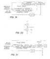
- Better noise characteristics and lower driver requirements may be achieved using a modified circuit, shown in figure 22. The circuit of figure 22 uses a modulation injection scheme similar to that of figure 7. Referring to figure 22, a difference engine receives an analog frequency produced by a VCO and a modulated numeric frequency bitstream. An output signal of the difference engine is filtered using a digital filter, which is followed by a DAC. In an exemplary embodiment, the DAC is a Sigma-Delta DAC that outputs a waveform the period of which is modulated in accordance with the applied voltage. The output signal of the DAC is applied through a resistor to an integrating capacitor C2 (no charge pump current sources are used). The voltage stored on the integrating capacitor is applied to the VCO.
- A separate modulation path is used to inject a modulation voltage into the circuit in accordance with the principles previous elucidated. A digital modulation signal is applied to a modulation DAC (also Sigma-Delta). An output signal of the modulation DAC is applied through a resistor to a capacitor C1, which forms a capacitive divider network with the integrating capacitor C2, after the manner of Figure 7. The series RC combination in the modulation path has a desirable filtering effect on the output signal of the modulation DAC.
- Note that modulation is injected at two different points in the circuit, through the main loop and through the separate modulation path. When the modulation is changed, it is changed at these two different points at the same time. To ensure proper operation, it becomes necessary to "dose" part of the modulation signal from the separate modulation path to the main loop. To accomplish this dosing, the modulation input signal of the separate modulation path is scaled by a factor K and input to the summing DAC of the main loop. In an exemplary embodiment, K = C1/(C1 + C2).
- Referring to Figure 23, in an alternative embodiment, the foregoing dosing may be performed in analog fashion using a resistor R2 coupled from the output of the DAC in the modulation path to the top plate of the integrating capacitor. In an exemplary embodiment, R1/R2 = C1/C2.


Claims (11)
- A phase lock loop, comprising :means responsive to an waveform having a frequency attribute and an input bitstream representing a desired waveform for producing an output bitstream representing a difference quantity between the analog waveform and the desired waveform;a filter and a digital to analog converter cooperating to produce a filtered analog difference signal;a controlled oscillator that produces the analog waveform; anda first capacitor coupling the filtered analog difference signal and an input terminal of the controlled oscillator.
- The apparatus of claim 1, wherein the filter is a digital filter.
- The apparatus of claim 2, wherein the first capacitor is a shunt capacitor having one plate coupled to a circuit reference potential.
- The apparatus of claim 2, further comprising a separate modulation path for injecting a modulation signal into a main loop of the phase lock loop, a modulation signal produced within the separate modulation path being coupled to an input terminal of the controlled oscillator by at least said first capacitor.
- The apparatus of claim 4, further comprising a second capacitor that together with said first capacitor forms a capacitive divider, wherein the modulation signal is applied to the input terminal of the controlled oscillator through the capacitive divider.
- The apparatus of claim 5, wherein the second capacitor is a series capacitor.
- The apparatus of claim 6, further comprising a resistor coupled in series with the second capacitor.
- The apparatus of claim 7, wherein the filtered analog difference signal is applied through a resistor to the first capacitor.
- The apparatus of claim 4, further comprising a bypass path between the separate modulation path and the main loop of the phase lock loop, the bypass path bypassing the second capacitor.
- The apparatus of claim 9, wherein the bypass path comprises a digital scaler.
- The apparatus of claim 9, wherein the bypass path comprises a resistor.
Applications Claiming Priority (2)
| Application Number | Priority Date | Filing Date | Title |
|---|---|---|---|
| US09/268,731US6094101A (en) | 1999-03-17 | 1999-03-17 | Direct digital frequency synthesis enabling spur elimination |
| EP00919409AEP1214790B1 (en) | 1999-03-17 | 2000-03-16 | Direct digital frequency synthesis enabling spur elimination |
Related Parent Applications (1)
| Application Number | Title | Priority Date | Filing Date |
|---|---|---|---|
| EP00919409ADivisionEP1214790B1 (en) | 1999-03-17 | 2000-03-16 | Direct digital frequency synthesis enabling spur elimination |
Publications (2)
| Publication Number | Publication Date |
|---|---|
| EP1619790A1true EP1619790A1 (en) | 2006-01-25 |
| EP1619790B1 EP1619790B1 (en) | 2007-09-12 |
Family
ID=23024224
Family Applications (2)
| Application Number | Title | Priority Date | Filing Date |
|---|---|---|---|
| EP00919409AExpired - LifetimeEP1214790B1 (en) | 1999-03-17 | 2000-03-16 | Direct digital frequency synthesis enabling spur elimination |
| EP05107961AExpired - LifetimeEP1619790B1 (en) | 1999-03-17 | 2000-03-16 | Direct digital frequency synthesis enabling spur elimination |
Family Applications Before (1)
| Application Number | Title | Priority Date | Filing Date |
|---|---|---|---|
| EP00919409AExpired - LifetimeEP1214790B1 (en) | 1999-03-17 | 2000-03-16 | Direct digital frequency synthesis enabling spur elimination |
Country Status (11)
| Country | Link |
|---|---|
| US (1) | US6094101A (en) |
| EP (2) | EP1214790B1 (en) |
| JP (1) | JP4452410B2 (en) |
| KR (1) | KR100696756B1 (en) |
| CN (1) | CN1211915C (en) |
| AT (2) | ATE373337T1 (en) |
| AU (1) | AU4010300A (en) |
| DE (2) | DE60036426T2 (en) |
| ES (1) | ES2251370T3 (en) |
| TW (1) | TW486872B (en) |
| WO (1) | WO2000055973A2 (en) |
Families Citing this family (51)
| Publication number | Priority date | Publication date | Assignee | Title |
|---|---|---|---|---|
| US6526265B1 (en)* | 1999-09-14 | 2003-02-25 | Skyworks Solutions, Inc. | Wireless transmitter having a modified translation loop architecture |
| FR2804808B1 (en)* | 2000-02-03 | 2002-03-15 | Ipanema Technologies | METHOD FOR DYNAMIC OPTIMIZATION OF QUALITY OF SERVICE IN A DATA TRANSMISSION NETWORK |
| GB0202884D0 (en) | 2002-02-07 | 2002-03-27 | Nokia Corp | Synthesiser |
| US7302237B2 (en) | 2002-07-23 | 2007-11-27 | Mercury Computer Systems, Inc. | Wideband signal generators, measurement devices, methods of signal generation, and methods of signal analysis |
| US6891432B2 (en) | 2002-11-14 | 2005-05-10 | Mia-Com, Inc. | Apparatus, methods and articles of manufacture for electromagnetic processing |
| US7340007B2 (en)* | 2003-09-16 | 2008-03-04 | M/A-Com, Inc. | Apparatus, methods and articles of manufacture for pre-emphasis filtering of a modulated signal |
| KR20050083741A (en)* | 2002-10-08 | 2005-08-26 | 엠/에이-컴, 인크. | Apparatus and method for adaptively re-aligning a modulated output signal |
| US7298854B2 (en)* | 2002-12-04 | 2007-11-20 | M/A-Com, Inc. | Apparatus, methods and articles of manufacture for noise reduction in electromagnetic signal processing |
| US7203262B2 (en)* | 2003-05-13 | 2007-04-10 | M/A-Com, Inc. | Methods and apparatus for signal modification in a fractional-N phase locked loop system |
| US6924699B2 (en)* | 2003-03-06 | 2005-08-02 | M/A-Com, Inc. | Apparatus, methods and articles of manufacture for digital modification in electromagnetic signal processing |
| US7545865B2 (en)* | 2002-12-03 | 2009-06-09 | M/A-Com, Inc. | Apparatus, methods and articles of manufacture for wideband signal processing |
| US7526260B2 (en)* | 2002-11-14 | 2009-04-28 | M/A-Com Eurotec, B.V. | Apparatus, methods and articles of manufacture for linear signal modification |
| US7245183B2 (en)* | 2002-11-14 | 2007-07-17 | M/A-Com Eurotec Bv | Apparatus, methods and articles of manufacture for processing an electromagnetic wave |
| US7187231B2 (en)* | 2002-12-02 | 2007-03-06 | M/A-Com, Inc. | Apparatus, methods and articles of manufacture for multiband signal processing |
| US7551685B2 (en)* | 2003-08-25 | 2009-06-23 | M/A-Com, Inc. | Apparatus, methods and articles of manufacture for signal correction using adaptive phase re-alignment |
| US6859098B2 (en) | 2003-01-17 | 2005-02-22 | M/A-Com, Inc. | Apparatus, methods and articles of manufacture for control in an electromagnetic processor |
| US7447272B2 (en) | 2003-04-22 | 2008-11-04 | Freescale Semiconductor, Inc. | Filter method and apparatus for polar modulation |
| US7091778B2 (en) | 2003-09-19 | 2006-08-15 | M/A-Com, Inc. | Adaptive wideband digital amplifier for linearly modulated signal amplification and transmission |
| US7480511B2 (en)* | 2003-09-19 | 2009-01-20 | Trimble Navigation Limited | Method and system for delivering virtual reference station data |
| US7343138B2 (en)* | 2003-12-08 | 2008-03-11 | M/A-Com, Inc. | Compensating for load pull in electromagentic signal propagation using adaptive impedance matching |
| US7356091B2 (en)* | 2003-12-09 | 2008-04-08 | M/A-Com, Inc. | Apparatus, methods and articles of manufacture for signal propagation using unwrapped phase |
| US6937175B1 (en) | 2004-04-21 | 2005-08-30 | Hrl Laboratories, Llc | Amplifier linearization using delta-sigma predistortion |
| US7026846B1 (en) | 2004-07-09 | 2006-04-11 | Analog Devices, Inc. | Synthesizer structures and methods that reduce spurious signals |
| US20070018699A1 (en)* | 2005-07-20 | 2007-01-25 | M/A-Com, Inc. | Partial cascode phase locked loop architecture |
| US20070018701A1 (en)* | 2005-07-20 | 2007-01-25 | M/A-Com, Inc. | Charge pump apparatus, system, and method |
| US7610023B2 (en)* | 2005-07-22 | 2009-10-27 | Pine Valley Investments, Inc. | Voltage controlled oscillator band switching system |
| US7417513B2 (en)* | 2005-08-17 | 2008-08-26 | M/A-Com, Inc. | System and method for signal filtering in a phase-locked loop system |
| DE102005050621B4 (en)* | 2005-10-21 | 2011-06-01 | Infineon Technologies Ag | Phase-locked loop and method for operating a phase locked loop |
| US7636386B2 (en)* | 2005-11-15 | 2009-12-22 | Panasonic Corporation | Method of continuously calibrating the gain for a multi-path angle modulator |
| US7482885B2 (en)* | 2005-12-29 | 2009-01-27 | Orca Systems, Inc. | Method of frequency synthesis for fast switching |
| US7599448B2 (en)* | 2006-02-03 | 2009-10-06 | Pine Valley Investments, Inc. | Multi-mode selectable modulation architecture calibration and power control apparatus, system, and method for radio frequency power amplifier |
| US7599418B2 (en)* | 2006-02-16 | 2009-10-06 | Pine Valley Investments, Inc. | Method and apparatus for a frequency hopper |
| US7519349B2 (en)* | 2006-02-17 | 2009-04-14 | Orca Systems, Inc. | Transceiver development in VHF/UHF/GSM/GPS/bluetooth/cordless telephones |
| US20070216455A1 (en)* | 2006-03-17 | 2007-09-20 | M/A-Com, Inc. | Partial cascode delay locked loop architecture |
| DE102006017973B4 (en)* | 2006-04-13 | 2014-05-28 | Atmel Corp. | Direct modulating frequency modulator |
| FR2905040B1 (en)* | 2006-08-21 | 2008-10-31 | St Microelectronics Sa | METHOD FOR PRODUCING A DIGITAL WORD REPRESENTATIVE OF A NON-WHOLE REPORT BETWEEN THE RESPECTIVE PERIODS OF TWO SIGNALS, AND CORRESPONDING DEVICE |
| US7649428B2 (en)* | 2007-03-13 | 2010-01-19 | Pine Valley Investments, Inc. | Method and system for generating noise in a frequency synthesizer |
| US8223909B2 (en)* | 2007-06-15 | 2012-07-17 | Panasonic Corporation | Digital sampling apparatuses and methods |
| US20090253398A1 (en)* | 2008-04-04 | 2009-10-08 | Sheehy Paul B | Modulation and upconversion techniques |
| US7786771B2 (en)* | 2008-05-27 | 2010-08-31 | Taiwan Semiconductor Manufacturing Company, Ltd. | Phase lock loop (PLL) with gain control |
| US7746187B2 (en)* | 2008-06-02 | 2010-06-29 | Panasonic Corporation | Self-calibrating modulator apparatuses and methods |
| US7983643B2 (en)* | 2008-07-03 | 2011-07-19 | Panasonic Corporation | Frequency demodulation with threshold extension |
| US20100009641A1 (en)* | 2008-07-11 | 2010-01-14 | Matsushita Electric Industrial Co.,Ltd. | Digital rf phase control in polar modulation transmitters |
| US7848266B2 (en) | 2008-07-25 | 2010-12-07 | Analog Devices, Inc. | Frequency synthesizers for wireless communication systems |
| US20100097150A1 (en)* | 2008-10-16 | 2010-04-22 | Keisuke Ueda | Pll circuit |
| KR20120082817A (en)* | 2009-08-28 | 2012-07-24 | 마크로스 저팬 주식회사 | Mobile telephone communication function disabling apparatus |
| US8339165B2 (en)* | 2009-12-07 | 2012-12-25 | Qualcomm Incorporated | Configurable digital-analog phase locked loop |
| US8446191B2 (en)* | 2009-12-07 | 2013-05-21 | Qualcomm Incorporated | Phase locked loop with digital compensation for analog integration |
| JP2011151473A (en)* | 2010-01-19 | 2011-08-04 | Panasonic Corp | Angle modulator, transmitter and wireless communication device |
| CN102651649B (en)* | 2012-03-14 | 2014-06-18 | 北京航空航天大学 | Design method of low-phase-noise microwave wideband frequency combiner |
| JP6331918B2 (en)* | 2014-09-19 | 2018-05-30 | 三菱電機株式会社 | Phase synchronization circuit |
Citations (5)
| Publication number | Priority date | Publication date | Assignee | Title |
|---|---|---|---|---|
| JPS59101910A (en)* | 1982-12-02 | 1984-06-12 | Fujitsu Ltd | Frequency modulator |
| US4746880A (en) | 1987-02-06 | 1988-05-24 | Digital Rf Solutions Corporation | Number controlled modulated oscillator |
| WO1991007828A1 (en)* | 1989-11-09 | 1991-05-30 | Roger Reed | Digital circuit for a frequency modulation and carrier synthesis in a digital radio system |
| US5028887A (en)* | 1989-08-31 | 1991-07-02 | Qualcomm, Inc. | Direct digital synthesizer driven phase lock loop frequency synthesizer with hard limiter |
| US5247469A (en) | 1991-05-23 | 1993-09-21 | Proxim, Inc. | Digital frequency synthesizer and method with vernier interpolation |
Family Cites Families (8)
| Publication number | Priority date | Publication date | Assignee | Title |
|---|---|---|---|---|
| GB2228840B (en)* | 1989-03-04 | 1993-02-10 | Racal Dana Instr Ltd | Frequency synthesisers |
| JPH0763124B2 (en)* | 1993-02-24 | 1995-07-05 | 日本電気株式会社 | Direct digital frequency synthesizer |
| JPH06343041A (en)* | 1993-06-01 | 1994-12-13 | Nippon Telegr & Teleph Corp <Ntt> | Synthesizer circuit |
| FR2717971A1 (en)* | 1994-03-23 | 1995-09-29 | Trt Telecom Radio Electr | Device for synthesizing a signal form, transmitter station and receiver station comprising such a device. |
| JP2836526B2 (en)* | 1995-04-10 | 1998-12-14 | 日本電気株式会社 | Frequency synthesizer |
| JPH10242762A (en)* | 1997-02-21 | 1998-09-11 | Kokusai Electric Co Ltd | Direct digital synthesizer oscillator |
| US5952895A (en)* | 1998-02-23 | 1999-09-14 | Tropian, Inc. | Direct digital synthesis of precise, stable angle modulated RF signal |
| JP4794433B2 (en)* | 2003-03-11 | 2011-10-19 | ファルマシア コーポレーション | S- [2-[(1-Iminoethyl) amino] ethyl] -2-methyl-L-cysteine maleate hydrochloride crystalline salt |
- 1999
- 1999-03-17USUS09/268,731patent/US6094101A/ennot_activeExpired - Lifetime
- 2000
- 2000-03-16TWTW089104818Apatent/TW486872B/ennot_activeIP Right Cessation
- 2000-03-16ATAT05107961Tpatent/ATE373337T1/ennot_activeIP Right Cessation
- 2000-03-16AUAU40103/00Apatent/AU4010300A/ennot_activeAbandoned
- 2000-03-16DEDE60036426Tpatent/DE60036426T2/ennot_activeExpired - Lifetime
- 2000-03-16EPEP00919409Apatent/EP1214790B1/ennot_activeExpired - Lifetime
- 2000-03-16ATAT00919409Tpatent/ATE308159T1/ennot_activeIP Right Cessation
- 2000-03-16WOPCT/US2000/006757patent/WO2000055973A2/enactiveIP Right Grant
- 2000-03-16CNCNB008063265Apatent/CN1211915C/ennot_activeExpired - Fee Related
- 2000-03-16EPEP05107961Apatent/EP1619790B1/ennot_activeExpired - Lifetime
- 2000-03-16DEDE60023526Tpatent/DE60023526T2/ennot_activeExpired - Lifetime
- 2000-03-16KRKR1020017011763Apatent/KR100696756B1/ennot_activeExpired - Fee Related
- 2000-03-16JPJP2000605310Apatent/JP4452410B2/ennot_activeExpired - Fee Related
- 2000-03-16ESES00919409Tpatent/ES2251370T3/ennot_activeExpired - Lifetime
Patent Citations (5)
| Publication number | Priority date | Publication date | Assignee | Title |
|---|---|---|---|---|
| JPS59101910A (en)* | 1982-12-02 | 1984-06-12 | Fujitsu Ltd | Frequency modulator |
| US4746880A (en) | 1987-02-06 | 1988-05-24 | Digital Rf Solutions Corporation | Number controlled modulated oscillator |
| US5028887A (en)* | 1989-08-31 | 1991-07-02 | Qualcomm, Inc. | Direct digital synthesizer driven phase lock loop frequency synthesizer with hard limiter |
| WO1991007828A1 (en)* | 1989-11-09 | 1991-05-30 | Roger Reed | Digital circuit for a frequency modulation and carrier synthesis in a digital radio system |
| US5247469A (en) | 1991-05-23 | 1993-09-21 | Proxim, Inc. | Digital frequency synthesizer and method with vernier interpolation |
Non-Patent Citations (1)
| Title |
|---|
| PATENT ABSTRACTS OF JAPAN vol. 008, no. 217 (E - 270) 4 October 1984 (1984-10-04)* |
Also Published As
| Publication number | Publication date |
|---|---|
| ATE308159T1 (en) | 2005-11-15 |
| CN1211915C (en) | 2005-07-20 |
| DE60023526D1 (en) | 2005-12-01 |
| DE60036426D1 (en) | 2007-10-25 |
| KR20020010894A (en) | 2002-02-06 |
| AU4010300A (en) | 2000-10-04 |
| TW486872B (en) | 2002-05-11 |
| JP4452410B2 (en) | 2010-04-21 |
| CN1347588A (en) | 2002-05-01 |
| EP1214790B1 (en) | 2005-10-26 |
| ATE373337T1 (en) | 2007-09-15 |
| DE60023526T2 (en) | 2006-07-20 |
| WO2000055973A2 (en) | 2000-09-21 |
| EP1619790B1 (en) | 2007-09-12 |
| KR100696756B1 (en) | 2007-03-19 |
| JP2002539705A (en) | 2002-11-19 |
| DE60036426T2 (en) | 2008-06-05 |
| WO2000055973A3 (en) | 2000-12-28 |
| US6094101A (en) | 2000-07-25 |
| EP1214790A2 (en) | 2002-06-19 |
| ES2251370T3 (en) | 2006-05-01 |
Similar Documents
| Publication | Publication Date | Title |
|---|---|---|
| US6094101A (en) | Direct digital frequency synthesis enabling spur elimination | |
| US8537957B2 (en) | Clock synchroniser | |
| US10158366B2 (en) | Digital fractional-N PLL based upon ring oscillator delta-sigma frequency conversion | |
| US6630868B2 (en) | Digitally-synthesized loop filter circuit particularly useful for a phase locked loop | |
| JP4283441B2 (en) | Accurate and stable direct digital synthesis of angle-modulated RF signals | |
| US20070126484A1 (en) | Fractional-n frequency synthesizer | |
| US6900675B2 (en) | All digital PLL trimming circuit | |
| TW200822566A (en) | Methods and systems for generating a clock signal, and a phase locked loop | |
| US7298218B2 (en) | Frequency synthesizer architecture | |
| US20030050030A1 (en) | Generation of a phase locked loop output signal having reduced spurious spectral components | |
| US7576615B2 (en) | Multi-point modulation and VCO compensation | |
| Brigati et al. | Modeling of fractional-N division frequency synthesizers with SIMULINK and MATLAB | |
| US7038509B1 (en) | Method and system for providing a phase-locked loop with reduced spurious tones | |
| US6418174B1 (en) | Frequency shift key modulator | |
| Kennedy et al. | Nonlinearity-induced spurs in fractional-N frequency synthesizers | |
| KR101242670B1 (en) | Sigma-delta based phase lock loop | |
| Rhee | Multi-bit delta-sigma modulation technique for fractional-N frequency synthesizers | |
| CN110289857B (en) | Clock generating circuit | |
| CN107294531A (en) | Phase-locked loop and frequency divider | |
| Hsu | Techniques for high-performance digital frequency synthesis and phase control. | |
| Rahkonen et al. | Low-power time-to-digital and digital-to-time converters for novel implementations of telecommunication building blocks | |
| EP1890382B1 (en) | Phase locked loop with improved linearity | |
| Filiol | Sigma-delta modulation for FM mobile radio. | |
| Walkington | New approaches in noise-shaping fractional-n synthesis | |
| Karsani | A dual-loop frequency synthesizer |
Legal Events
| Date | Code | Title | Description |
|---|---|---|---|
| PUAI | Public reference made under article 153(3) epc to a published international application that has entered the european phase | Free format text:ORIGINAL CODE: 0009012 | |
| AC | Divisional application: reference to earlier application | Ref document number:1214790 Country of ref document:EP Kind code of ref document:P | |
| AK | Designated contracting states | Kind code of ref document:A1 Designated state(s):AT BE CH CY DE DK ES FI FR GB GR IE IT LI LU MC NL PT SE | |
| AX | Request for extension of the european patent | Extension state:AL BA HR MK YU | |
| 17P | Request for examination filed | Effective date:20060724 | |
| 17Q | First examination report despatched | Effective date:20060828 | |
| AKX | Designation fees paid | Designated state(s):AT BE CH CY DE DK ES FI FR GB GR IE IT LI LU MC NL PT SE | |
| RAP1 | Party data changed (applicant data changed or rights of an application transferred) | Owner name:MATSUSHITA ELECTRIC INDUSTRIAL CO., LTD. | |
| 17Q | First examination report despatched | Effective date:20060828 | |
| GRAP | Despatch of communication of intention to grant a patent | Free format text:ORIGINAL CODE: EPIDOSNIGR1 | |
| GRAS | Grant fee paid | Free format text:ORIGINAL CODE: EPIDOSNIGR3 | |
| GRAA | (expected) grant | Free format text:ORIGINAL CODE: 0009210 | |
| AC | Divisional application: reference to earlier application | Ref document number:1214790 Country of ref document:EP Kind code of ref document:P | |
| AK | Designated contracting states | Kind code of ref document:B1 Designated state(s):AT BE CH CY DE DK ES FI FR GB GR IE IT LI LU MC NL PT SE | |
| REG | Reference to a national code | Ref country code:GB Ref legal event code:FG4D | |
| REG | Reference to a national code | Ref country code:CH Ref legal event code:EP | |
| REF | Corresponds to: | Ref document number:60036426 Country of ref document:DE Date of ref document:20071025 Kind code of ref document:P | |
| REG | Reference to a national code | Ref country code:IE Ref legal event code:FG4D | |
| PG25 | Lapsed in a contracting state [announced via postgrant information from national office to epo] | Ref country code:FI Free format text:LAPSE BECAUSE OF FAILURE TO SUBMIT A TRANSLATION OF THE DESCRIPTION OR TO PAY THE FEE WITHIN THE PRESCRIBED TIME-LIMIT Effective date:20070912 | |
| PG25 | Lapsed in a contracting state [announced via postgrant information from national office to epo] | Ref country code:CH Free format text:LAPSE BECAUSE OF FAILURE TO SUBMIT A TRANSLATION OF THE DESCRIPTION OR TO PAY THE FEE WITHIN THE PRESCRIBED TIME-LIMIT Effective date:20070912 Ref country code:LI Free format text:LAPSE BECAUSE OF FAILURE TO SUBMIT A TRANSLATION OF THE DESCRIPTION OR TO PAY THE FEE WITHIN THE PRESCRIBED TIME-LIMIT Effective date:20070912 Ref country code:AT Free format text:LAPSE BECAUSE OF FAILURE TO SUBMIT A TRANSLATION OF THE DESCRIPTION OR TO PAY THE FEE WITHIN THE PRESCRIBED TIME-LIMIT Effective date:20070912 | |
| NLV1 | Nl: lapsed or annulled due to failure to fulfill the requirements of art. 29p and 29m of the patents act | ||
| PG25 | Lapsed in a contracting state [announced via postgrant information from national office to epo] | Ref country code:BE Free format text:LAPSE BECAUSE OF FAILURE TO SUBMIT A TRANSLATION OF THE DESCRIPTION OR TO PAY THE FEE WITHIN THE PRESCRIBED TIME-LIMIT Effective date:20070912 | |
| REG | Reference to a national code | Ref country code:CH Ref legal event code:PL | |
| PG25 | Lapsed in a contracting state [announced via postgrant information from national office to epo] | Ref country code:NL Free format text:LAPSE BECAUSE OF FAILURE TO SUBMIT A TRANSLATION OF THE DESCRIPTION OR TO PAY THE FEE WITHIN THE PRESCRIBED TIME-LIMIT Effective date:20070912 Ref country code:GR Free format text:LAPSE BECAUSE OF FAILURE TO SUBMIT A TRANSLATION OF THE DESCRIPTION OR TO PAY THE FEE WITHIN THE PRESCRIBED TIME-LIMIT Effective date:20071213 Ref country code:ES Free format text:LAPSE BECAUSE OF FAILURE TO SUBMIT A TRANSLATION OF THE DESCRIPTION OR TO PAY THE FEE WITHIN THE PRESCRIBED TIME-LIMIT Effective date:20071223 | |
| PG25 | Lapsed in a contracting state [announced via postgrant information from national office to epo] | Ref country code:PT Free format text:LAPSE BECAUSE OF FAILURE TO SUBMIT A TRANSLATION OF THE DESCRIPTION OR TO PAY THE FEE WITHIN THE PRESCRIBED TIME-LIMIT Effective date:20080212 | |
| PG25 | Lapsed in a contracting state [announced via postgrant information from national office to epo] | Ref country code:SE Free format text:LAPSE BECAUSE OF FAILURE TO SUBMIT A TRANSLATION OF THE DESCRIPTION OR TO PAY THE FEE WITHIN THE PRESCRIBED TIME-LIMIT Effective date:20071212 | |
| PLBE | No opposition filed within time limit | Free format text:ORIGINAL CODE: 0009261 | |
| STAA | Information on the status of an ep patent application or granted ep patent | Free format text:STATUS: NO OPPOSITION FILED WITHIN TIME LIMIT | |
| PG25 | Lapsed in a contracting state [announced via postgrant information from national office to epo] | Ref country code:DK Free format text:LAPSE BECAUSE OF FAILURE TO SUBMIT A TRANSLATION OF THE DESCRIPTION OR TO PAY THE FEE WITHIN THE PRESCRIBED TIME-LIMIT Effective date:20070912 | |
| 26N | No opposition filed | Effective date:20080613 | |
| PG25 | Lapsed in a contracting state [announced via postgrant information from national office to epo] | Ref country code:MC Free format text:LAPSE BECAUSE OF NON-PAYMENT OF DUE FEES Effective date:20080331 | |
| PG25 | Lapsed in a contracting state [announced via postgrant information from national office to epo] | Ref country code:IE Free format text:LAPSE BECAUSE OF NON-PAYMENT OF DUE FEES Effective date:20080317 | |
| PG25 | Lapsed in a contracting state [announced via postgrant information from national office to epo] | Ref country code:CY Free format text:LAPSE BECAUSE OF FAILURE TO SUBMIT A TRANSLATION OF THE DESCRIPTION OR TO PAY THE FEE WITHIN THE PRESCRIBED TIME-LIMIT Effective date:20070912 | |
| PG25 | Lapsed in a contracting state [announced via postgrant information from national office to epo] | Ref country code:LU Free format text:LAPSE BECAUSE OF NON-PAYMENT OF DUE FEES Effective date:20080316 | |
| PG25 | Lapsed in a contracting state [announced via postgrant information from national office to epo] | Ref country code:IT Free format text:LAPSE BECAUSE OF NON-PAYMENT OF DUE FEES Effective date:20080331 | |
| PG25 | Lapsed in a contracting state [announced via postgrant information from national office to epo] | Ref country code:FR Free format text:LAPSE BECAUSE OF FAILURE TO SUBMIT A TRANSLATION OF THE DESCRIPTION OR TO PAY THE FEE WITHIN THE PRESCRIBED TIME-LIMIT Effective date:20070912 | |
| REG | Reference to a national code | Ref country code:DE Ref legal event code:R081 Ref document number:60036426 Country of ref document:DE Owner name:APPLE INC., CUPERTINO, US Free format text:FORMER OWNER: PANASONIC CORPORATION, KADOMA-SHI, OSAKA, JP Ref country code:DE Ref legal event code:R082 Ref document number:60036426 Country of ref document:DE Representative=s name:DR. GASSNER & PARTNER MBB PATENTANWAELTE, DE Ref country code:DE Ref legal event code:R081 Ref document number:60036426 Country of ref document:DE Owner name:INTEL CORPORATION (N.D.GES.D. STAATES DELAWARE, US Free format text:FORMER OWNER: PANASONIC CORPORATION, KADOMA-SHI, OSAKA, JP | |
| REG | Reference to a national code | Ref country code:GB Ref legal event code:732E Free format text:REGISTERED BETWEEN 20160901 AND 20160907 | |
| PGFP | Annual fee paid to national office [announced via postgrant information from national office to epo] | Ref country code:GB Payment date:20170315 Year of fee payment:18 | |
| GBPC | Gb: european patent ceased through non-payment of renewal fee | Effective date:20180316 | |
| PG25 | Lapsed in a contracting state [announced via postgrant information from national office to epo] | Ref country code:GB Free format text:LAPSE BECAUSE OF NON-PAYMENT OF DUE FEES Effective date:20180316 | |
| PGFP | Annual fee paid to national office [announced via postgrant information from national office to epo] | Ref country code:DE Payment date:20190305 Year of fee payment:20 | |
| REG | Reference to a national code | Ref country code:DE Ref legal event code:R071 Ref document number:60036426 Country of ref document:DE | |
| REG | Reference to a national code | Ref country code:DE Ref legal event code:R082 Ref document number:60036426 Country of ref document:DE Representative=s name:DR. GASSNER & PARTNER MBB PATENTANWAELTE, DE Ref country code:DE Ref legal event code:R081 Ref document number:60036426 Country of ref document:DE Owner name:APPLE INC., CUPERTINO, US Free format text:FORMER OWNER: INTEL CORPORATION (N.D.GES.D. STAATES DELAWARE), SANTA CLARA, CALIF., US |