EP1596346A1 - Closed loop transmitter control for power amplifier in an eas system - Google Patents
Closed loop transmitter control for power amplifier in an eas systemDownload PDFInfo
- Publication number
- EP1596346A1 EP1596346A1EP05010094AEP05010094AEP1596346A1EP 1596346 A1EP1596346 A1EP 1596346A1EP 05010094 AEP05010094 AEP 05010094AEP 05010094 AEP05010094 AEP 05010094AEP 1596346 A1EP1596346 A1EP 1596346A1
- Authority
- EP
- European Patent Office
- Prior art keywords
- current
- modulator
- control
- transmitter
- sensed
- Prior art date
- Legal status (The legal status is an assumption and is not a legal conclusion. Google has not performed a legal analysis and makes no representation as to the accuracy of the status listed.)
- Granted
Links
Images


Classifications
- G—PHYSICS
- G08—SIGNALLING
- G08B—SIGNALLING OR CALLING SYSTEMS; ORDER TELEGRAPHS; ALARM SYSTEMS
- G08B13/00—Burglar, theft or intruder alarms
- G08B13/22—Electrical actuation
- G08B13/24—Electrical actuation by interference with electromagnetic field distribution
- G08B13/2402—Electronic Article Surveillance [EAS], i.e. systems using tags for detecting removal of a tagged item from a secure area, e.g. tags for detecting shoplifting
- G08B13/2465—Aspects related to the EAS system, e.g. system components other than tags
- G08B13/2468—Antenna in system and the related signal processing
- G08B13/2477—Antenna or antenna activator circuit
- G—PHYSICS
- G08—SIGNALLING
- G08B—SIGNALLING OR CALLING SYSTEMS; ORDER TELEGRAPHS; ALARM SYSTEMS
- G08B13/00—Burglar, theft or intruder alarms
- G08B13/22—Electrical actuation
- G08B13/24—Electrical actuation by interference with electromagnetic field distribution
- G08B13/2402—Electronic Article Surveillance [EAS], i.e. systems using tags for detecting removal of a tagged item from a secure area, e.g. tags for detecting shoplifting
- G08B13/2405—Electronic Article Surveillance [EAS], i.e. systems using tags for detecting removal of a tagged item from a secure area, e.g. tags for detecting shoplifting characterised by the tag technology used
- G08B13/2408—Electronic Article Surveillance [EAS], i.e. systems using tags for detecting removal of a tagged item from a secure area, e.g. tags for detecting shoplifting characterised by the tag technology used using ferromagnetic tags
- G—PHYSICS
- G08—SIGNALLING
- G08B—SIGNALLING OR CALLING SYSTEMS; ORDER TELEGRAPHS; ALARM SYSTEMS
- G08B13/00—Burglar, theft or intruder alarms
- G08B13/22—Electrical actuation
- G08B13/24—Electrical actuation by interference with electromagnetic field distribution
- G08B13/2402—Electronic Article Surveillance [EAS], i.e. systems using tags for detecting removal of a tagged item from a secure area, e.g. tags for detecting shoplifting
- G08B13/2465—Aspects related to the EAS system, e.g. system components other than tags
- G08B13/2468—Antenna in system and the related signal processing
- G08B13/2471—Antenna signal processing by receiver or emitter
Definitions
- This inventionrelates generally to signal generation within an electronic article surveillance system and, more particularly, to a system and method for amplifier control within a transmitter configured to transmit signals for reception by EAS tags.
- a detection systemmay excite an EAS tag by transmitting an electromagnetic burst at a resonance frequency of the tag.
- the tagWhen the tag is present within the electromagnetic field created by the transmission burst, the tag begins to resonate with an acoustomagnetic or magnetomechanical response frequency that is detectable by a receiver in the detection system.
- Transmitters used in these detection systemsmay include linear amplifiers using feedback control or switching amplifiers using open loop control.
- Linear amplifiersprovide good transmitter current regulation with feedback control, but are expensive because of poor power efficiency, typically around forty-five percent (45%).
- Previous switching amplifiersprovide good power efficiency, typically around eighty-five percent (85%), but transmitter current levels can fluctuate due to the open loop control and variable load conditions.
- Controller components of the prior artattempt to mitigate this current fluctuation by providing a low bandwidth pulse width adjustment based on measured currents from previous transmission bursts.
- transmitter component hardwareprovides a single pulse width modulator that controls a single half bridge amplifier with multiple loads connected in parallel across the amplifier output.
- the antenna with the lowest impedancereceives more current than antennas with higher impedance, resulting in different levels of transmission, or power, being output from each of the antennas.
- the current sensing hardware in such prior art systemsis such that only the current supplied to a single load can be sensed at any given time. Specifically, the current applied to a load is estimated after the entire transmission burst is completed by averaging the current samples.
- a method for controlling a transmitter in an electronic article surveillance systemmay comprise coupling each of a plurality of transmit channels of the transmitter to a corresponding antenna, configuring a modulator within each transmit channel to output a modulated signal to the corresponding antenna, providing feedback of each modulated signal, and adjusting operation of each modulator based on the feedback.
- a transmitter for an electronic article surveillance systemis provided.
- the transmittermay comprise a plurality of antennas configured for transmission of signals and a plurality of transmit channels.
- Each transmit channelis coupled to a corresponding one of the antennas, and each comprises an amplifier configured to supply a signal to its antenna, a modulator configured to supply a modulated signal to the amplifier, a sensing circuit configured to sense an amount of current applied to the antenna by the amplifier, and a controller configured to receive the sensed current amount from the sensing circuit.
- the controlleris configured to control operation of the modulator based on the sensed current amount.
- an electronic article surveillance systemmay comprise at least one tag, at least one receiver configured to receive emissions from the tag, and at least one transmitter comprising a plurality of transmit channels.
- Each transmit channelmay be configured to transmit signals to cause the tag to resonate when the tag is in a vicinity of the transmit channel.
- Each transmit channelmay be independently configured to utilize feedback to control an output power of the transmit channel.
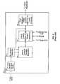
- FIG. 1is a block diagram of a transmitter 10 for an electronic article surveillance (EAS) system.
- the transmitter 10may include a plurality of antennas 12, 14, 16, and 18 respectively, that transmit a signal received from an amplifier 20.
- a controller 30 within the transmitter 10may be configured to provide a low bandwidth pulse width adjustment based on current measurements taken during previous transmission bursts.
- the controller 30may include a single pulse width modulator 32 that controls the amplifier 20, which in one embodiment, may be a single half bridge amplifier, with the antennas 12, 14, 16, and 18 connected in parallel across amplifier output 22.
- current sense circuits 34, 36, 38, and 40may be electrically connected to each respective antenna 12, 14, 16, and 18 and configured to sense an amount of current delivered to each respective antenna 12, 14, 16, and 18.
- the current sense circuits 34, 36, 38, and 40each provide a measure of current applied to the antennas 12, 14, 16, and 18 to a muxing circuit 42.
- the muxing circuit 42may be controlled by a control algorithm component 44.
- the control algorithm component 44determines which current sense circuit output is to be switched through muxing circuit 42 for processing by an analog-to-digital converter 46. Therefore, and in a sequence controlled by the control algorithm component 44, an amount of current applied to each antenna 12, 14, 16, and 18 is fed back through the A/D converter 46 and the control algorithm component 44 to control operation of the pulse width modulator 32.
- the antennas 12, 14, 16, and 18function as a current divider, and the antenna with the lowest impedance receives more current than the antennas having higher impedances.
- each antenna 12, 14, 16, and 18typically has a slightly different impedance and therefore transmits a different amount of power. This may be undesirable in an EAS system transmitter.
- the current sensing hardware in such a systemi.e., the current sense circuits 34, 36, 38, and 40 and the muxing circuit 42
- the current applied to each loadis estimated after the transmission burst is completed by averaging the current samples received at the control algorithm 44.
- FIG. 2is a block diagram illustrating the functionality of the control algorithm component 44. Specifically, a sample buffer 60 receives samples of the sensed current that is applied to the antennas 12, 14, 16, and 18 from the A/D converter 46 (all shown in FIG. 1). As described above, sample buffer 60 receives samples relating to a single one of antennas 12, 14, 16, and 18 at any one time. The samples are then processed to determine an amplitude of the samples by a envelope detector 62 as is known.
- the amplitude of the sensed current sampleis then input into a pulse width modulator control update equation 68.
- the pulse width modulator (PWM) control values 70receives inputs relating to a transmit frequency, phase of the transmit signal, and a desired current output of the PWM hardware.
- a calculation component 72may be configured to determine minimum PWM control values 70, sometimes referred to as state variables, for the loads being driven by the PWM hardware, via amplifier 20 (shown in FIG. 1).
- FIG. 3is an illustration of an embodiment of a multiple channel transmitter 100 for an EAS system that addresses the different antenna impedances and resultant variations in transmit power described above.
- four independent transmitter channels 102, 104, 106 and 108are illustrated, but it is understood that any number of transmitter channels may be utilized as necessary for a given EAS system application.
- transmitter channel 102While described with respect to transmitter channel 102 below, it is to be understood that transmitter channels 104, 106, and 108 may be similarly configured. In addition, any embodiments that utilize less than or more than four transmitter channels may be similarly configured.
- the transmitter 100utilizes real-time feedback control of individual switching power amplifiers.
- each transmitter channelfor example transmitter channel 102, may include an independent switching amplifier 110 provided with real-time feedback control of the pulse width modulator 112.
- Such a configurationprovides the power efficiency and low cost of switching amplifiers, with a level of current regulation similar to that commonly associated with linear amplifiers. Because the power generated within each independent transmitter channel in this embodiment is approximately one fourth the power generated within a transmitter using a single channel (and amplifier) to drive four antennas (e.g., transmitter 10 shown in FIG.
- the transmitter channel 102may include a current sensing circuit 114 configured to measure, or sense, an amount of current that the amplifier 110 supplies to drive the load provided by antenna 116.
- current sensing circuit 114may be configured to output a voltage.
- the current sensing circuit 114provides a feedback signal 118 (e.g., a voltage), which may be input into an analog-to-digital converter (ADC) 120 and converted to a digital signal 122.
- ADCanalog-to-digital converter
- This digital signal 122may be input into a control algorithm component 124.
- Control algorithm component 124includes, for example, a processing chip, such as a microprocessor, microcontroller or digital signal processor (DSP) and the programming associated therewith.
- a processing chipsuch as a microprocessor, microcontroller or digital signal processor (DSP) and the programming associated therewith.
- DSPdigital signal processor
- the control algorithm component 124may be implemented using combinations of discrete electronic components.
- FIG. 4Operation of an embodiment of a control algorithm component 124 is illustrated in FIG. 4.
- the digital signal 122which is representative of the current sensed at the output of the amplifier 110, may be input into the control algorithm component 124.
- the control algorithm component 124may be configured to determine the magnitude of the feedback signal.
- magnitude of the digital signal 122may be determined using an envelope detector 130 as is known. Those of ordinary skill in the art will appreciate that other known detectors may be used.
- the magnitude of the digital signal 122may be input into a proportional, integral, derivative, or "PID", controller 150.
- a desired current amplituderepresented by set point 152
- the error signal 154may then be multiplied by a proportional gain constant 160, or Kp, to produce the proportional control value 162, or Cp.
- the error signal 154may also input into an integrator equation, shown as discrete integrator 170 in FIG. 4, whose output 172 is multiplied by the integral gain constant 174, or Ki, to produce the integral control value 176, or Ci.
- error signal 154may also be input into a differentiator equation, shown as discrete differentiator 180 in FIG. 4, whose output 182 may be multiplied by the derivative gain constant 184, or Kd, to produce the differential control value 186, or Cd.
- the three control component values 162, 176, and 186, or Cp, Ci, and Cd,may be summed to produce a overall control value 190, or C.
- This control value 190may be limited by a limiting function embodied within limiter 192 to an allowable input range of the pulse width modulator 112.
- the resulting control signal 194may be input into the pulse width modulator 112 (shown in FIG. 3).
- Implementation of discrete integral and differentiator equations on digital signal processors and other processing componentsgenerally is known to those skilled in the art.
- selection of suitable gain constants Kp, Ki, and Kdmay be dependent on other parameters of the system, such as variable gains in the current sense circuit 114 and the amplifier 110 due to variations in discrete electronic components.
- DSPdigital signal processor
- the signal processing described hereinis capable of being performed on microprocessors, microcontrollers, and other processing topologies, for example, fuzzy and/or neural control structures, observer/estimator or state space control structures, and other topologies, without altering the essence of the embodiments herein described.
- advances in semiconductor integrationhave produced a variety of integrated circuits that integrate, for example, muxing, analog to digital conversion, and modulation within a single processor chip.
- control signal 194 generated by the control algorithm component 124is therefore based upon an amount of current sensed at the antenna 116 by the current sense circuit 114 (both shown in FIG. 3).
- This control signal 194may be input into the pulse width modulator 112 (shown in FIG. 3), which generates a pulse modulated signal having a pulse width dependent upon the parameters of the control signal 194.
- the pulse modulated signal generatedmay then be amplified by the amplifier 110 (shown in FIG. 3) and used to drive the transmission antenna 116.
- the transmission pulse outputresults in a current applied to the antenna 116.
- the currentmay again be sensed by current sensing circuit 114, which provides feedback to the control algorithm component 124. In this way, feedback is utilized to set the width of the transmitted signal pulse output by the amplifier 110.
- the EAS system transmitter 100 described with respect to FIGS. 3 and 4provides independent real-time control of the amount of current applied to multiple antenna loads.
- an EAS transmittercan be configured so that a desired amount of transmit power can be individually controlled for each antenna of the transmitter 100 through simultaneous, independent, current monitoring of all transmit channels 102, 104, 106, and 108.
- cost of the transmitteris reduced to due semiconductor integration and also due to the reduction in power (both generated and dissipated) associated with separate transmit channels.
- a net effect of higher integration and smaller, less expensive power componentsis that the total cost of using multiple independent transmit channels and loads is less than using a single channel to supply power for multiple loads.
- the transmitter configurations described hereinalso result in advantages with respect to circuit protection, thermal management, and current regulation as compared to known transmitter configurations.
- FIG. 5is an illustration of an EAS system 200 which is capable of incorporating the embodiments of transmitter 100 described herein.
- EAS system 200may include a first antenna pedestal 202 and a second antenna pedestal 204, each of which may include a number of antennas (e.g., antenna 16).
- the antennas within antenna pedestals 202 and 204may be connected to a control unit 206 that may include transmitter 100 and receiver 210.
- a controller 212may be configured for communication with an external device.
- controller 212may be configured to control the timing of transmissions from transmitter 100 and expected receptions at receiver 210 such that the antenna pedestals 202 and 204 can be utilized for both transmission of signals to an EAS tag 220 and reception of frequencies generated by EAS tag 220.
- System 200is representative of many EAS systems and is meant as an example only.
- control unit 206may be located within one of the antenna pedestals 202 and 204.
- additional antennaswhich only receive frequencies from the EAS tags 220 may be utilized as part of the EAS system 200.
- a single control unit 206either within a pedestal or located separately, may be configured to control multiple sets of antenna pedestals.
- the performance of the transmitterse.g., transmitter 100
- EAS systemse.g., EAS system 200
- the performance of the transmittersis improved to provide an increase in power efficiency and to allow the independent sensing of multiple antenna loads.
- such transmittersprovide reliable transmitter current levels under variable load conditions and also provide redundant fault handling at a low cost.
Landscapes
- Physics & Mathematics (AREA)
- Engineering & Computer Science (AREA)
- General Physics & Mathematics (AREA)
- Computer Security & Cryptography (AREA)
- Automation & Control Theory (AREA)
- Electromagnetism (AREA)
- Signal Processing (AREA)
- Amplifiers (AREA)
- Burglar Alarm Systems (AREA)
- Transmitters (AREA)
- Near-Field Transmission Systems (AREA)
- Closed-Circuit Television Systems (AREA)
- Emergency Alarm Devices (AREA)
- Radar Systems Or Details Thereof (AREA)
Abstract
Description
Claims (21)
- A method for controlling a transmitter in an electronic article surveillancesystem, said method comprising:coupling each of a plurality of transmit channels of the transmitter to acorresponding antenna;configuring a modulator within each transmit channel to output amodulated signal to the corresponding antenna;providing feedback of each modulated signal; andadjusting operation of each modulator based on the feedback.
- A method according to claim 1 wherein adjusting operation of themodulator comprises adjusting a width of each pulse modulated signal applied tothe corresponding antenna.
- A method according to claim 1 wherein providing feedback of eachmodulated signal comprises:sensing an amount of current applied to the antenna; andconverting the sensed current to a digital value.
- A method according to claim 1 wherein adjusting operation of themodulator comprises adjusting a width of each pulse modulated signal applied tothe corresponding antenna utilizing a proportional, integral, differential controller.
- A method according to claim 1 wherein adjusting operation of eachmodulator comprises:sensing an amount of current applied to the corresponding antenna; andconfiguring a proportional, integral, differential control function to reducean error between a magnitude of the sensed current and a desired current value.
- A method according to claim 1 wherein adjusting operation of eachmodulator comprises:sensing an amount of current applied to the corresponding antenna;configuring a proportional, integral, differential (PID) control function toreduce an error between the sensed current magnitude and a desired current value;andprogramming the PID control function to output a control value to alimiting function, where the control value is configured to include proportional,integral, and differential components.
- A transmitter for an electronic article surveillance system comprising:a plurality of antennas configured for transmission of signals; anda plurality of transmit channels, each of said transmit channels coupled toat least a corresponding one or more of said antennas, each of said transmitchannels comprising:an amplifier configured to provide a signal to the corresponding saidantenna;a modulator configured to provide a modulated signal to said amplifier;a sensing circuit configured to sense an amount of current applied to saidantenna by said amplifier; anda controller configured to receive the sensed current amount from saidsensing circuit, said controller configured to control operation of said modulatorbased on the sensed current amount.
- A transmitter according to claim 7 wherein said modulator comprises apulse width modulator.
- A transmitter according to claim 7 wherein said amplifier comprises aswitching amplifier.
- A transmitter according to claim 7 further comprising an analog-to-digital(A/D) converter, said A/D converter configured to convert the sensed current to adigital value, the digital value received by said controller.
- A transmitter according to claim 7 wherein said controller comprises aproportional, integral, differential controller.
- A transmitter according to claim 7 wherein said controller comprises:a mathematical component configured to determine a magnitude of thesensed current; anda proportional, integral, differential controller configured to receive thesensed current magnitude and reduce an error between the sensed magnitude anda desired current value.
- A transmitter according to claim 7 wherein said modulator comprises apulse width modulator and said controller comprises:a mathematical component configured to determine a magnitude of thesensed current;a limiting function configured to limit an output of said controller to anallowable range of said pulse width modulator; anda proportional, integral, differential controller configured to receive thesensed current magnitude, reduce an error between the sensed magnitude and adesired current value, and output a control value to said limiting function, thecontrol value including proportional, integral, and differential components.
- An electronic article surveillance system comprising:at least one tag;at least one receiver configured to receive emissions from said tag; andat least one transmitter comprising a plurality of transmit channels, eachsaid transmit channel configured to transmit signals to cause said tag to resonatewhen said tag is in a vicinity of said transmit channel, each said transmit channelindependently configured to utilize feedback to control an output power of saidtransmit channel.
- An electronic article surveillance system according to claim 14 whereineach said transmitter channel comprises:at least one antenna;a modulator configured to supply a modulated signal to said at least oneantenna;a sensing circuit configured to sense an amount of current applied to saidat least one antenna; anda control circuit is configured to receive the sensed current amount fromsaid sensing circuit, said control circuit configured to utilize the sensed currentamount to control operation of said modulator.
- An electronic article surveillance system according to claim 14 whereinsaid transmit channel comprises a pulse width modulator configured to utilizefeedback to control output power of said transmit channel.
- An electronic article surveillance system according to claim 14 whereinsaid transmit channel comprises:a sensing circuit configured to sense an amount of current output by saidtransmit channel; andan analog-to-digital (A/D) converter, said A/D converter configured toconvert the sensed current to a digital value, the digital value utilized to control anoutput power of said transmit channel.
- An electronic article surveillance system according to claim 14 whereinsaid transmit channel comprises:a modulator;a sensing circuit configured to sense an amount of current output by saidtransmit channel; anda proportional, integral, differential controller configured to receive anerror signal based on the sensed current amount from said sensing circuit, saidcontrol circuit configured to utilize the error signal to control operation of saidmodulator.
- An electronic article surveillance system according to claim 14 whereinsaid transmit channel comprises a proportional, integral, differential controllerconfigured to receive an error signal based on a sensed current magnitude andprovide an output configured to reduce the error between the sensed magnitudeand a desired current value.
- An electronic article surveillance system according to claim 14 whereinsaid transmit channel comprises:a modulator;a limiting function configured to limit a control value signal to anallowable range of said modulator; anda proportional, integral, differential controller configured to receive anerror signal based on a sensed current magnitude, and output a control valueconfigured to reduce an error between the sensed magnitude and a desired currentvalue to said limiting function, the control value including proportional, integral,and differential components.
- A method to control the generation of a pulsed signal in an EAS systemcomprising:generating a plurality of pulse modulated signals;independently driving a load with each of said plurality of pulse modulatedsignals;sensing a current at each load driven by said pulse modulated signal togenerate a current sense signal for each load; andusing each of said current sense signals to adjust the width of each pulsemodulated signal used to drive its respective load.
Applications Claiming Priority (4)
| Application Number | Priority Date | Filing Date | Title |
|---|---|---|---|
| US57003204P | 2004-05-11 | 2004-05-11 | |
| US570032P | 2004-05-11 | ||
| US121897 | 2005-05-04 | ||
| US11/121,897US7301459B2 (en) | 2004-05-11 | 2005-05-04 | Closed loop transmitter control for power amplifier in an EAS system |
Publications (2)
| Publication Number | Publication Date |
|---|---|
| EP1596346A1true EP1596346A1 (en) | 2005-11-16 |
| EP1596346B1 EP1596346B1 (en) | 2008-07-23 |
Family
ID=34936323
Family Applications (1)
| Application Number | Title | Priority Date | Filing Date |
|---|---|---|---|
| EP05010094AExpired - LifetimeEP1596346B1 (en) | 2004-05-11 | 2005-05-10 | Closed loop transmitter control for power amplifier in an eas system |
Country Status (7)
| Country | Link |
|---|---|
| US (1) | US7301459B2 (en) |
| EP (1) | EP1596346B1 (en) |
| JP (1) | JP4275100B2 (en) |
| AT (1) | ATE402461T1 (en) |
| CA (1) | CA2507033C (en) |
| DE (1) | DE602005008306D1 (en) |
| ES (1) | ES2310306T3 (en) |
Cited By (2)
| Publication number | Priority date | Publication date | Assignee | Title |
|---|---|---|---|---|
| US8587489B2 (en) | 2007-06-08 | 2013-11-19 | Checkpoint Systems, Inc. | Dynamic EAS detection system and method |
| US8933790B2 (en) | 2007-06-08 | 2015-01-13 | Checkpoint Systems, Inc. | Phase coupler for rotating fields |
Families Citing this family (1)
| Publication number | Priority date | Publication date | Assignee | Title |
|---|---|---|---|---|
| US7768353B2 (en) | 2008-06-13 | 2010-08-03 | Samsung Electro-Mechanics Company, Ltd. | Systems and methods for switching mode power amplifier control |
Citations (4)
| Publication number | Priority date | Publication date | Assignee | Title |
|---|---|---|---|---|
| US4683461A (en)* | 1985-09-17 | 1987-07-28 | Allied Corporation | Inductive magnetic field generator |
| US5239696A (en)* | 1991-10-15 | 1993-08-24 | Sensormatic Electronics Corporation | Linear power amplifier utilizing current feedback |
| US5963173A (en)* | 1997-12-05 | 1999-10-05 | Sensormatic Electronics Corporation | Antenna and transmitter arrangement for EAS system |
| US20020196144A1 (en)* | 2001-06-13 | 2002-12-26 | Belka Anthony Michael | Field creation in a magnetic electronic article surveillance system |
Family Cites Families (6)
| Publication number | Priority date | Publication date | Assignee | Title |
|---|---|---|---|---|
| US5103234A (en)* | 1987-08-28 | 1992-04-07 | Sensormatic Electronics Corporation | Electronic article surveillance system |
| US4859991A (en)* | 1987-08-28 | 1989-08-22 | Sensormatic Electronics Corporation | Electronic article surveillance system employing time domain and/or frequency domain analysis and computerized operation |
| US5608758A (en)* | 1992-07-15 | 1997-03-04 | Futaba Denshi Kogyo, K.K. | Radio control device having crystal high frequency module and high frequency phase lockloop for selective use, modules detachably mounted |
| US5742189A (en)* | 1994-09-16 | 1998-04-21 | Kabushiki Kaisha Toshiba | Frequency conversion circuit and radio communication apparatus with the same |
| KR0168222B1 (en)* | 1995-12-27 | 1999-03-20 | 김주용 | Output power measurement and high frequency output stabilization circuit for each channel in a system using a linear power amplifier |
| US6970518B2 (en)* | 2003-03-11 | 2005-11-29 | Motorola, Inc. | Method and apparatus for electronic item identification in a communication system using known source parameters |
- 2005
- 2005-05-04USUS11/121,897patent/US7301459B2/enactiveActive
- 2005-05-10ESES05010094Tpatent/ES2310306T3/ennot_activeExpired - Lifetime
- 2005-05-10CACA002507033Apatent/CA2507033C/ennot_activeExpired - Lifetime
- 2005-05-10EPEP05010094Apatent/EP1596346B1/ennot_activeExpired - Lifetime
- 2005-05-10DEDE602005008306Tpatent/DE602005008306D1/ennot_activeExpired - Lifetime
- 2005-05-10ATAT05010094Tpatent/ATE402461T1/ennot_activeIP Right Cessation
- 2005-05-11JPJP2005138122Apatent/JP4275100B2/ennot_activeExpired - Lifetime
Patent Citations (4)
| Publication number | Priority date | Publication date | Assignee | Title |
|---|---|---|---|---|
| US4683461A (en)* | 1985-09-17 | 1987-07-28 | Allied Corporation | Inductive magnetic field generator |
| US5239696A (en)* | 1991-10-15 | 1993-08-24 | Sensormatic Electronics Corporation | Linear power amplifier utilizing current feedback |
| US5963173A (en)* | 1997-12-05 | 1999-10-05 | Sensormatic Electronics Corporation | Antenna and transmitter arrangement for EAS system |
| US20020196144A1 (en)* | 2001-06-13 | 2002-12-26 | Belka Anthony Michael | Field creation in a magnetic electronic article surveillance system |
Cited By (2)
| Publication number | Priority date | Publication date | Assignee | Title |
|---|---|---|---|---|
| US8587489B2 (en) | 2007-06-08 | 2013-11-19 | Checkpoint Systems, Inc. | Dynamic EAS detection system and method |
| US8933790B2 (en) | 2007-06-08 | 2015-01-13 | Checkpoint Systems, Inc. | Phase coupler for rotating fields |
Also Published As
| Publication number | Publication date |
|---|---|
| ES2310306T3 (en) | 2009-01-01 |
| DE602005008306D1 (en) | 2008-09-04 |
| EP1596346B1 (en) | 2008-07-23 |
| US7301459B2 (en) | 2007-11-27 |
| CA2507033C (en) | 2009-07-14 |
| CA2507033A1 (en) | 2005-11-11 |
| US20050253719A1 (en) | 2005-11-17 |
| HK1086676A1 (en) | 2006-09-22 |
| ATE402461T1 (en) | 2008-08-15 |
| JP2005328535A (en) | 2005-11-24 |
| JP4275100B2 (en) | 2009-06-10 |
Similar Documents
| Publication | Publication Date | Title |
|---|---|---|
| US5339041A (en) | High efficiency power amplifier | |
| EP0509733B1 (en) | Radio-frequency power amplifier device | |
| WO2002078179A2 (en) | Digital signal processor enhanced pulse width modulation amplifier | |
| JPH02285817A (en) | Radio transmitter | |
| JP2007509546A (en) | Additional adjustment of the reference signal for automatic power control in mobile terminals | |
| US20230231477A1 (en) | Power supply controller | |
| US7301459B2 (en) | Closed loop transmitter control for power amplifier in an EAS system | |
| US6876197B2 (en) | Transmission arrangement for a magnetic resonance apparatus | |
| CN106972870B (en) | A kind of antenna tuning circuit, mobile terminal and antenna tuning method | |
| HK1086676B (en) | Transmitter for an electronic article surveillance system and method for controlling the same | |
| EP1598679A1 (en) | Radio frequency pulse amplifier with control loops for compensating phase and amplitude deviations | |
| US6265940B1 (en) | Detector and transmitter incorporating the detector | |
| CA2507037C (en) | Active transmitter ringdown for switching power amplifier | |
| US20070109863A1 (en) | Power regulation in radio-frequency transmitters | |
| CN100557986C (en) | Transmitter for electronic article surveillance system and control method thereof | |
| US5903192A (en) | Arrangement for controlling the output amplitude of a high frequency power amplifier | |
| JPH07288434A (en) | Power amplifier | |
| US5714908A (en) | Power correction method and circuit | |
| US20040176153A1 (en) | Transmitter control circuit | |
| JPH11186862A (en) | Level control system | |
| CN100422766C (en) | Active Transmitter Loop-Down for Switching Power Amplifiers | |
| JP2005012610A (en) | Detection circuit, detection method and transmitter-receiver | |
| KR100415524B1 (en) | A gain control circuit and method for providing gain control of a variable amplifier using a pilot signal | |
| DE10140897A1 (en) | Method for controlling the output power of a transmit / receive module of an active phase-controlled radar antenna | |
| JP2005130227A (en) | Detection circuit |
Legal Events
| Date | Code | Title | Description |
|---|---|---|---|
| PUAI | Public reference made under article 153(3) epc to a published international application that has entered the european phase | Free format text:ORIGINAL CODE: 0009012 | |
| 17P | Request for examination filed | Effective date:20050728 | |
| AK | Designated contracting states | Kind code of ref document:A1 Designated state(s):AT BE BG CH CY CZ DE DK EE ES FI FR GB GR HU IE IS IT LI LT LU MC NL PL PT RO SE SI SK TR | |
| AX | Request for extension of the european patent | Extension state:AL BA HR LV MK YU | |
| AKX | Designation fees paid | Designated state(s):AT BE BG CH CY CZ DE DK EE ES FI FR GB GR HU IE IS IT LI LT LU MC NL PL PT RO SE SI SK TR | |
| 17Q | First examination report despatched | Effective date:20060530 | |
| 17Q | First examination report despatched | Effective date:20060530 | |
| GRAP | Despatch of communication of intention to grant a patent | Free format text:ORIGINAL CODE: EPIDOSNIGR1 | |
| GRAS | Grant fee paid | Free format text:ORIGINAL CODE: EPIDOSNIGR3 | |
| GRAA | (expected) grant | Free format text:ORIGINAL CODE: 0009210 | |
| AK | Designated contracting states | Kind code of ref document:B1 Designated state(s):AT BE BG CH CY CZ DE DK EE ES FI FR GB GR HU IE IS IT LI LT LU MC NL PL PT RO SE SI SK TR | |
| REG | Reference to a national code | Ref country code:GB Ref legal event code:FG4D | |
| REG | Reference to a national code | Ref country code:CH Ref legal event code:EP | |
| REG | Reference to a national code | Ref country code:IE Ref legal event code:FG4D | |
| REF | Corresponds to: | Ref document number:602005008306 Country of ref document:DE Date of ref document:20080904 Kind code of ref document:P | |
| REG | Reference to a national code | Ref country code:SE Ref legal event code:TRGR | |
| REG | Reference to a national code | Ref country code:ES Ref legal event code:FG2A Ref document number:2310306 Country of ref document:ES Kind code of ref document:T3 | |
| NLV1 | Nl: lapsed or annulled due to failure to fulfill the requirements of art. 29p and 29m of the patents act | ||
| PG25 | Lapsed in a contracting state [announced via postgrant information from national office to epo] | Ref country code:IS Free format text:LAPSE BECAUSE OF FAILURE TO SUBMIT A TRANSLATION OF THE DESCRIPTION OR TO PAY THE FEE WITHIN THE PRESCRIBED TIME-LIMIT Effective date:20081123 Ref country code:LT Free format text:LAPSE BECAUSE OF FAILURE TO SUBMIT A TRANSLATION OF THE DESCRIPTION OR TO PAY THE FEE WITHIN THE PRESCRIBED TIME-LIMIT Effective date:20080723 Ref country code:NL Free format text:LAPSE BECAUSE OF FAILURE TO SUBMIT A TRANSLATION OF THE DESCRIPTION OR TO PAY THE FEE WITHIN THE PRESCRIBED TIME-LIMIT Effective date:20080723 Ref country code:PT Free format text:LAPSE BECAUSE OF FAILURE TO SUBMIT A TRANSLATION OF THE DESCRIPTION OR TO PAY THE FEE WITHIN THE PRESCRIBED TIME-LIMIT Effective date:20081223 | |
| PG25 | Lapsed in a contracting state [announced via postgrant information from national office to epo] | Ref country code:AT Free format text:LAPSE BECAUSE OF FAILURE TO SUBMIT A TRANSLATION OF THE DESCRIPTION OR TO PAY THE FEE WITHIN THE PRESCRIBED TIME-LIMIT Effective date:20080723 Ref country code:SI Free format text:LAPSE BECAUSE OF FAILURE TO SUBMIT A TRANSLATION OF THE DESCRIPTION OR TO PAY THE FEE WITHIN THE PRESCRIBED TIME-LIMIT Effective date:20080723 Ref country code:FI Free format text:LAPSE BECAUSE OF FAILURE TO SUBMIT A TRANSLATION OF THE DESCRIPTION OR TO PAY THE FEE WITHIN THE PRESCRIBED TIME-LIMIT Effective date:20080723 Ref country code:BG Free format text:LAPSE BECAUSE OF FAILURE TO SUBMIT A TRANSLATION OF THE DESCRIPTION OR TO PAY THE FEE WITHIN THE PRESCRIBED TIME-LIMIT Effective date:20081023 | |
| PG25 | Lapsed in a contracting state [announced via postgrant information from national office to epo] | Ref country code:BE Free format text:LAPSE BECAUSE OF FAILURE TO SUBMIT A TRANSLATION OF THE DESCRIPTION OR TO PAY THE FEE WITHIN THE PRESCRIBED TIME-LIMIT Effective date:20080723 | |
| PG25 | Lapsed in a contracting state [announced via postgrant information from national office to epo] | Ref country code:EE Free format text:LAPSE BECAUSE OF FAILURE TO SUBMIT A TRANSLATION OF THE DESCRIPTION OR TO PAY THE FEE WITHIN THE PRESCRIBED TIME-LIMIT Effective date:20080723 Ref country code:DK Free format text:LAPSE BECAUSE OF FAILURE TO SUBMIT A TRANSLATION OF THE DESCRIPTION OR TO PAY THE FEE WITHIN THE PRESCRIBED TIME-LIMIT Effective date:20080723 | |
| PG25 | Lapsed in a contracting state [announced via postgrant information from national office to epo] | Ref country code:SK Free format text:LAPSE BECAUSE OF FAILURE TO SUBMIT A TRANSLATION OF THE DESCRIPTION OR TO PAY THE FEE WITHIN THE PRESCRIBED TIME-LIMIT Effective date:20080723 Ref country code:RO Free format text:LAPSE BECAUSE OF FAILURE TO SUBMIT A TRANSLATION OF THE DESCRIPTION OR TO PAY THE FEE WITHIN THE PRESCRIBED TIME-LIMIT Effective date:20080723 Ref country code:CZ Free format text:LAPSE BECAUSE OF FAILURE TO SUBMIT A TRANSLATION OF THE DESCRIPTION OR TO PAY THE FEE WITHIN THE PRESCRIBED TIME-LIMIT Effective date:20080723 | |
| PLBE | No opposition filed within time limit | Free format text:ORIGINAL CODE: 0009261 | |
| STAA | Information on the status of an ep patent application or granted ep patent | Free format text:STATUS: NO OPPOSITION FILED WITHIN TIME LIMIT | |
| 26N | No opposition filed | Effective date:20090424 | |
| PG25 | Lapsed in a contracting state [announced via postgrant information from national office to epo] | Ref country code:MC Free format text:LAPSE BECAUSE OF NON-PAYMENT OF DUE FEES Effective date:20090531 | |
| REG | Reference to a national code | Ref country code:CH Ref legal event code:PL | |
| PG25 | Lapsed in a contracting state [announced via postgrant information from national office to epo] | Ref country code:CH Free format text:LAPSE BECAUSE OF NON-PAYMENT OF DUE FEES Effective date:20090531 Ref country code:LI Free format text:LAPSE BECAUSE OF NON-PAYMENT OF DUE FEES Effective date:20090531 | |
| PG25 | Lapsed in a contracting state [announced via postgrant information from national office to epo] | Ref country code:IE Free format text:LAPSE BECAUSE OF NON-PAYMENT OF DUE FEES Effective date:20090510 | |
| PG25 | Lapsed in a contracting state [announced via postgrant information from national office to epo] | Ref country code:PL Free format text:LAPSE BECAUSE OF FAILURE TO SUBMIT A TRANSLATION OF THE DESCRIPTION OR TO PAY THE FEE WITHIN THE PRESCRIBED TIME-LIMIT Effective date:20080723 | |
| PG25 | Lapsed in a contracting state [announced via postgrant information from national office to epo] | Ref country code:GR Free format text:LAPSE BECAUSE OF FAILURE TO SUBMIT A TRANSLATION OF THE DESCRIPTION OR TO PAY THE FEE WITHIN THE PRESCRIBED TIME-LIMIT Effective date:20081024 | |
| REG | Reference to a national code | Ref country code:GB Ref legal event code:732E Free format text:REGISTERED BETWEEN 20101111 AND 20101117 | |
| PG25 | Lapsed in a contracting state [announced via postgrant information from national office to epo] | Ref country code:LU Free format text:LAPSE BECAUSE OF NON-PAYMENT OF DUE FEES Effective date:20090510 | |
| PG25 | Lapsed in a contracting state [announced via postgrant information from national office to epo] | Ref country code:HU Free format text:LAPSE BECAUSE OF FAILURE TO SUBMIT A TRANSLATION OF THE DESCRIPTION OR TO PAY THE FEE WITHIN THE PRESCRIBED TIME-LIMIT Effective date:20090124 | |
| PG25 | Lapsed in a contracting state [announced via postgrant information from national office to epo] | Ref country code:TR Free format text:LAPSE BECAUSE OF FAILURE TO SUBMIT A TRANSLATION OF THE DESCRIPTION OR TO PAY THE FEE WITHIN THE PRESCRIBED TIME-LIMIT Effective date:20080723 | |
| PG25 | Lapsed in a contracting state [announced via postgrant information from national office to epo] | Ref country code:CY Free format text:LAPSE BECAUSE OF FAILURE TO SUBMIT A TRANSLATION OF THE DESCRIPTION OR TO PAY THE FEE WITHIN THE PRESCRIBED TIME-LIMIT Effective date:20080723 | |
| REG | Reference to a national code | Ref country code:FR Ref legal event code:TP Owner name:SENSORMATIC ELECTRONICS, LLC, US Effective date:20110913 | |
| REG | Reference to a national code | Ref country code:DE Ref legal event code:R082 Ref document number:602005008306 Country of ref document:DE Representative=s name:HAFNER & PARTNER, DE | |
| REG | Reference to a national code | Ref country code:DE Ref legal event code:R081 Ref document number:602005008306 Country of ref document:DE Owner name:TYCO FIRE & SECURITY GMBH, CH Free format text:FORMER OWNER: SENSORMATIC ELECTRONICS, LLC, BOCA RATON, FLA., US Effective date:20130612 Ref country code:DE Ref legal event code:R082 Ref document number:602005008306 Country of ref document:DE Representative=s name:HAFNER & KOHL, DE Effective date:20130612 Ref country code:DE Ref legal event code:R081 Ref document number:602005008306 Country of ref document:DE Owner name:TYCO FIRE & SECURITY GMBH, CH Free format text:FORMER OWNER: SENSORMATIC ELECTRONICS, LLC, BOCA RATON, US Effective date:20130612 Ref country code:DE Ref legal event code:R082 Ref document number:602005008306 Country of ref document:DE Representative=s name:HAFNER & PARTNER, DE Effective date:20130612 Ref country code:DE Ref legal event code:R082 Ref document number:602005008306 Country of ref document:DE Representative=s name:HAFNER & KOHL PATENTANWALTSKANZLEI RECHTSANWAL, DE Effective date:20130612 | |
| REG | Reference to a national code | Ref country code:GB Ref legal event code:732E Free format text:REGISTERED BETWEEN 20150205 AND 20150211 | |
| REG | Reference to a national code | Ref country code:GB Ref legal event code:732E Free format text:REGISTERED BETWEEN 20150305 AND 20150311 | |
| REG | Reference to a national code | Ref country code:FR Ref legal event code:PLFP Year of fee payment:11 | |
| REG | Reference to a national code | Ref country code:FR Ref legal event code:TP Owner name:TYCO FIRE & SECURITY GMBH, CH Effective date:20160115 | |
| REG | Reference to a national code | Ref country code:FR Ref legal event code:PLFP Year of fee payment:12 | |
| REG | Reference to a national code | Ref country code:FR Ref legal event code:PLFP Year of fee payment:13 | |
| REG | Reference to a national code | Ref country code:FR Ref legal event code:PLFP Year of fee payment:14 | |
| REG | Reference to a national code | Ref country code:DE Ref legal event code:R082 Ref document number:602005008306 Country of ref document:DE Representative=s name:HAFNER & KOHL PATENTANWALTSKANZLEI RECHTSANWAL, DE Ref country code:DE Ref legal event code:R081 Ref document number:602005008306 Country of ref document:DE Owner name:SENSORMATIC ELECTRONICS, LLC, BOCA RATON, US Free format text:FORMER OWNER: TYCO FIRE & SECURITY GMBH, NEUHAUSEN AM RHEINFALL, CH Ref country code:DE Ref legal event code:R082 Ref document number:602005008306 Country of ref document:DE Representative=s name:HAFNER & KOHL PATENT- UND RECHTSANWAELTE PARTN, DE Ref country code:DE Ref legal event code:R082 Ref document number:602005008306 Country of ref document:DE Representative=s name:HAFNER & KOHL PARTMBB, DE | |
| REG | Reference to a national code | Ref country code:GB Ref legal event code:732E Free format text:REGISTERED BETWEEN 20191205 AND 20191211 | |
| PGFP | Annual fee paid to national office [announced via postgrant information from national office to epo] | Ref country code:GB Payment date:20240521 Year of fee payment:20 | |
| PGFP | Annual fee paid to national office [announced via postgrant information from national office to epo] | Ref country code:DE Payment date:20240529 Year of fee payment:20 | |
| PGFP | Annual fee paid to national office [announced via postgrant information from national office to epo] | Ref country code:ES Payment date:20240610 Year of fee payment:20 | |
| PGFP | Annual fee paid to national office [announced via postgrant information from national office to epo] | Ref country code:FR Payment date:20240527 Year of fee payment:20 | |
| PGFP | Annual fee paid to national office [announced via postgrant information from national office to epo] | Ref country code:SE Payment date:20240527 Year of fee payment:20 | |
| PGFP | Annual fee paid to national office [announced via postgrant information from national office to epo] | Ref country code:IT Payment date:20240524 Year of fee payment:20 | |
| REG | Reference to a national code | Ref country code:DE Ref legal event code:R071 Ref document number:602005008306 Country of ref document:DE | |
| REG | Reference to a national code | Ref country code:ES Ref legal event code:FD2A Effective date:20250529 | |
| REG | Reference to a national code | Ref country code:GB Ref legal event code:PE20 Expiry date:20250509 | |
| REG | Reference to a national code | Ref country code:SE Ref legal event code:EUG | |
| PG25 | Lapsed in a contracting state [announced via postgrant information from national office to epo] | Ref country code:ES Free format text:LAPSE BECAUSE OF EXPIRATION OF PROTECTION Effective date:20250511 Ref country code:GB Free format text:LAPSE BECAUSE OF EXPIRATION OF PROTECTION Effective date:20250509 |