EP1583228A2 - Composite power amplifier - Google Patents
Composite power amplifierDownload PDFInfo
- Publication number
- EP1583228A2 EP1583228A2EP05011980AEP05011980AEP1583228A2EP 1583228 A2EP1583228 A2EP 1583228A2EP 05011980 AEP05011980 AEP 05011980AEP 05011980 AEP05011980 AEP 05011980AEP 1583228 A2EP1583228 A2EP 1583228A2
- Authority
- EP
- European Patent Office
- Prior art keywords
- amplifier
- output
- chireix
- doherty
- amplifiers
- Prior art date
- Legal status (The legal status is an assumption and is not a legal conclusion. Google has not performed a legal analysis and makes no representation as to the accuracy of the status listed.)
- Granted
Links
Images


Classifications
- H—ELECTRICITY
- H03—ELECTRONIC CIRCUITRY
- H03F—AMPLIFIERS
- H03F1/00—Details of amplifiers with only discharge tubes, only semiconductor devices or only unspecified devices as amplifying elements
- H03F1/02—Modifications of amplifiers to raise the efficiency, e.g. gliding Class A stages, use of an auxiliary oscillation
- H03F1/0205—Modifications of amplifiers to raise the efficiency, e.g. gliding Class A stages, use of an auxiliary oscillation in transistor amplifiers
- H03F1/0288—Modifications of amplifiers to raise the efficiency, e.g. gliding Class A stages, use of an auxiliary oscillation in transistor amplifiers using a main and one or several auxiliary peaking amplifiers whereby the load is connected to the main amplifier using an impedance inverter, e.g. Doherty amplifiers
- H—ELECTRICITY
- H03—ELECTRONIC CIRCUITRY
- H03F—AMPLIFIERS
- H03F1/00—Details of amplifiers with only discharge tubes, only semiconductor devices or only unspecified devices as amplifying elements
- H03F1/02—Modifications of amplifiers to raise the efficiency, e.g. gliding Class A stages, use of an auxiliary oscillation
- H03F1/0205—Modifications of amplifiers to raise the efficiency, e.g. gliding Class A stages, use of an auxiliary oscillation in transistor amplifiers
- H03F1/0294—Modifications of amplifiers to raise the efficiency, e.g. gliding Class A stages, use of an auxiliary oscillation in transistor amplifiers using vector summing of two or more constant amplitude phase-modulated signals
- H—ELECTRICITY
- H03—ELECTRONIC CIRCUITRY
- H03F—AMPLIFIERS
- H03F1/00—Details of amplifiers with only discharge tubes, only semiconductor devices or only unspecified devices as amplifying elements
- H03F1/32—Modifications of amplifiers to reduce non-linear distortion
- H—ELECTRICITY
- H03—ELECTRONIC CIRCUITRY
- H03F—AMPLIFIERS
- H03F3/00—Amplifiers with only discharge tubes or only semiconductor devices as amplifying elements
- H03F3/60—Amplifiers in which coupling networks have distributed constants, e.g. with waveguide resonators
- H03F3/602—Combinations of several amplifiers
- H—ELECTRICITY
- H03—ELECTRONIC CIRCUITRY
- H03F—AMPLIFIERS
- H03F2200/00—Indexing scheme relating to amplifiers
- H03F2200/423—Amplifier output adaptation especially for transmission line coupling purposes, e.g. impedance adaptation
Definitions
- the present inventionrelates generally to composite power amplifiers.
- the power amplifier (PA) in the transmitteris required to be very linear, in addition to being able to simultaneously amplify many radio channels (frequencies) spread across a fairly wide bandwidth. It also has to do this efficiently, in order to reduce power consumption and need for cooling, and to increase its longevity. High linearity is required since nonlinear amplifiers would cause leakage of interfering signal energy between channels.
- the amplitude probability density of a mix of sufficiently many independent radio frequency (RF) channels, or of a multi-user CDMA (Code Division Multiple Access) signaltends to be close to a Rayleigh distribution having a large peak-to-average power ratio. Since a conventional RF power amplifier generally has an efficiency proportional to its output amplitude, its average efficiency is very low for such signals.
- An object of the present inventionis a more flexible composite power amplifier, which can be used in both a Doherty and a Chireix type mode without excessive redesign or retuning.
- Another objectis an improved Chireix type composite amplifier.
- the present inventionprovides a flexible, robust, possibly multi-band, efficient composite amplifier by applying several new techniques.
- the strategyis to converge the input and output network structures, and to control signal shaping of Doherty and Chireix amplifiers to make the drive signals as similar as possible.
- efficient new operating modesthat lie between and outside of these pure modes can also used.
- the resulting continuum of high-efficiency modescan be obtained by using one output network and a common way of operating the input network.
- the modified output networkcan also be used in a new Chireix type composite amplifier, thereby eliminating the need for compensating reactances used in the prior art.
- Chireix type output network or combinerthe output networks of both Chireix and LINC amplifiers will be denoted Chireix type output network or combiner.
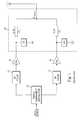
- Fig. 1is a block diagram of a typical prior art Chireix amplifier.
- Output network 20includes two quarter-wave lines ⁇ /4 and two compensating reactances +jX and -jX, which are used to extend the region of high efficiency to include lower output power levels.
- the efficiency of Chireix systemsis analyzed.
- [5, 6, 7]methods to overcome nonlinearity due to gain and phase imbalances are described.
- the Chireix methodhas also been used in broadcast transmitters under the trademark Ampliphase [6, 7].
- Chireix amplifierAn advantage of the Chireix amplifier is the ability to change the efficiency curve to suit different peak-to-average power ratios, by changing the size (X) of the reactances.
- the peak output poweris equally divided between the amplifiers irrespective of this adjustment, which means that equal size (capacity) amplifiers can be used.
- Fig. 2is a block diagram of a typical prior art Doherty amplifier.
- the Doherty amplifieruses one linear and one nonlinear power amplifier.
- the published theorystates that a main power amplifier 16 is driven as a linear amplifier in class B, and an auxiliary power amplifier 18 having nonlinear output current (through class C operation or some other technique represented by block 22) "modulates" the impedance seen by the main amplifier, through the impedance-inverting quarter-wave line [2, 10] in the output network 20. Since the nonlinear output current of the auxiliary amplifier is zero below a certain transition (output) voltage, the auxiliary amplifier does not contribute to the power loss below this voltage.
- An alternative output structure with built-in impedance matchingis described in [11, 12].
- the transition point of the standard Doherty amplifieris at half the maximum output voltage. With this transition point the efficiency curve is most suited for moderate peak-to-average power ratios, and the peak power is divided equally between the two constituent amplifiers.
- the transition point in the Doherty amplifiercan be changed by changing the impedance of the quarter-wave transmission line (or equivalent circuit). The efficiency curve can then be adjusted for higher peak-to-average power ratios, and the peak output power will be unequally divided between the amplifiers. Different size amplifiers will thus be needed for optimum utilization of the available peak power.
- a first step towards this new composite amplifieris to alter the structure of the output network of the Chireix amplifier to get rid of the reactances +jX and -jX.
- Thiscan be done by using shortened and lengthened versions of the quarter wavelength lines used in the prior art.
- the impedance Z L of theseis the optimum load impedance R opt for a class B amplifier, and the load impedance R LOAD should be half this value.
- the shortened and lengthened (by equal amounts ⁇ ) transmission linesact as quarter wave lines with the appropriate reactances.
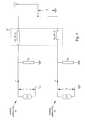
- the new output network structureis illustrated in Fig. 3 as output network 21.
- this output network structurecan be used also for making Doherty amplifiers, as illustrated in Fig. 4.
- the criteria that have to be fulfilledare:
- a second step towards the new composite amplifier in accordance with the present inventionis to alter the structure of the input network. Before this new structure is described it is useful to first describe typical prior art Chireix and Doherty input network structures.
- the Chireix amplifier drive signals from signal component separator 10 in Fig, 1include a linear plus or minus a nonlinear component (plus to one power amplifier and minus to the other power amplifier). These components are illustrated in Fig, 5.
- Fig. 6is a diagram similar to Fig. 5 illustrating the modification in accordance with the present invention.
- the basic idea of the modificationis to drive the composite amplifier linearly below a certain transition point T.P.
- T.Ptransition point
- the amplitude of the drive signalis constant, and the phase difference between the amplifiers is used to generate amplitude modulation at the output. Below the transition point this leads to excessive current consumption, because the voltage and current at each power amplifier will become more and more out of phase. The output power decreases but the transistor RF current (which can be translated to DC current) will not decrease.
- Fig. 7is a block diagram of an exemplary embodiment of a Chireix amplifier in accordance with the present invention.
- the linear drive signal componentsare produced by amplifier/phase shifter 26 and 32 directly from the input signal.
- nonlinear drive signal componentsare generated by a nonlinear element 38 and amplifier/phase shifter 28 and 30.
- the amplitude dependenceis linear up to the transition point T.P., and follows a linear approximation of the circle segment after the transition point.
- Unit 38may, for example, be implemented as a combination of a lookup table followed by D/A converters in which a digital input signal amplitude is transformed into the proper drive signals (the input signal amplitude is assumed to be proportional to the composite amplifier output voltage amplitude).
- analog implementationsare also possible.
- the nonlinear signal from amplifier/phase shifter 28is added to the linear signal component from amplifier/phase shifter 26 in an adder 34, while the nonlinear signal from amplifier/phase shifter 30 is subtracted from the linear signal component from amplifier/phase shifter 32 in an adder 36.
- adders 34, 36may, for example, be realized as hybrids.
- theyare digital adders.
- the composite amplifiermay be part of a transmitter, for example a transmitter in a radio terminal, such as a base station or a mobile station in a cellular mobile radio communication system.
- each of the drive signal componentswill include a common phase component. For this reason only three of the phases actually have to be adjusted.
- a method of adjusting the amplitudes and phases of the linear partsis to adjust them to obtain maximum power output and maximum efficiency at the maximum input excitation level (with otherwise linear behavior). This can be done in a model of the amplifier, to obtain adjustment factors, or in the amplifier itself. The result of this operation is amplifier performance and efficiency similar to a class-B amplifier using the same transistors.
- the amplitudes and phases of the nonlinear signal componentsare adjusted in order to minimize the average current consumption.
- This conditionusually allows at least one of the transistors to have constant and maximum output voltage. Since this procedure should preferably be performed while ensuring linearity in the output, the amplified nonlinear signals should cancel each other at the output. As will be shown below, it is possible to achieve such a cancellation. However, in order to explain how this is done, it will be necessary to introduce a model of the output network.
- Fig. 8illustrates such an output network model.
- the active part of the amplifier transistor outputsare modeled as linear controlled current generators.
- the finite output conductances of the transistorsare denoted z p1 and z p2 , respectively.
- a quantity of special interestis how RF currents from the output nodes of amplifiers 16 and 18 transform into voltages at the output node of the composite amplifier. This quantity is represented by the output transimpedances
- a simple way to fulfil this conditionis have a compensating filter in one of the nonlinear branches, for example z o1 * z o2 -1 in the lower branch (here "*" denotes convolution in the time domain and multiplication in the frequency domain).
- z o1 * z o2 -1in the lower branch
- *denotes convolution in the time domain and multiplication in the frequency domain.
- Another way to fulfill condition (1)is to insert the filter z o2 in the upper branch and the filter z o1 in the lower branch. In this way both branches will be subjected to the composite filter z o1 * z o2 .
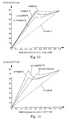
- Fig. 10is a diagram illustrating the relationship between output current and output voltage for an ideal conventional Doherty amplifier.
- Main power amplifier 16is driven by a linear signal
- auxiliary power amplifier 18is driven by a nonlinear signal, which is zero up to the transition point T.P. and varies linearly thereafter.
- T.P.transition point
- a conventional Doherty amplifierone amplifier is driven by a linear signal and the other amplifier is driven by a nonlinear signal, which is very different from a conventional Chireix amplifier, in which both amplifiers are driven by signals that include both linear and nonlinear components.
- Fig. 11is a diagram illustrating the relationship between output current components and output voltage for a Doherty amplifier that has been modified in accordance with the present invention.
- the idea of this modificationis to drive both amplifiers with a linear and a nonlinear drive signal component, just as in the Chireix case described above. This will (ideally) give the same output currents from each power amplifier as in Fig. 10.
- this modificationit is possible to drive the input network of a Doherty amplifier in the same way as the modified Chireix amplifier described above (but at another frequency).
- the same input network structure as in Fig. 9may be used also for the modified Doherty amplifier.
- the linear operation up to the maximum amplitude in the outputis obtained by application of the linear basis function alone.
- all RF voltages in the systemare less than or equal to their end values since they depend linearly on this function.
- the magnitudes and gains of the paths for the linear basis functioncan then be adjusted for achieving a partial objective, i.e. maximum peak power in the output, without the need for adjusting the paths for the nonlinear (triangular) function.
- the amplifier(without the effect of the triangular basis function) then works as an optimal class B amplifier. This is possible for the unified Chireix-Doherty output network of the present invention at all frequencies.
- the paths for the nonlinear basis functioncan be arbitrarily adjusted, without showing in the output, as long as condition (1) is met.
- An additional requirementis of course that nonlinear effects, such as saturation of the amplifiers, do not come into play in any significant way.
- the objective hereis to minimize the D.C. power (i.e. current) consumption, by setting the right magnitude and phase for the nonlinear basis function paths, under these conditions. This maximizes the efficiency.
- the RF voltagesare generally altered at both of the output amplifiers as a result, but as long as the voltages lie inside the maximum allowed, this has no major consequences.
- Another parameter that can be adjustedis the transition point T.P. where the output voltage of the triangular basis function has its maximum. This can be used for example if the optimum transition voltage is not known beforehand. In conjunction with this adjustment, an adjustment of the shape of the nonlinear basis function (to a curved shape) can, if necessary, be incorporated.
- the just described control strategyhas the advantages that it can be used for all composite amplifiers, that the peak output power can be independently optimized, and that the efficiency maximization does not affect the output signal.
- the resulting structure, with provisions for the adjustments,is shown in Fig. 12.
- the letter Gimplies a gain, P stands for phase, and T.P. means transition point.
- the phase of the linear part to one of the amplifierscan (as mentioned above) be left out of the adjustments. These adjustments are for one frequency or operating mode only. If wideband operation is desired, the further methods of [13] can be used.
- the unified control strategy using the triangular and linear basis functionsworks for all composite amplifiers.
- Amplifiers with the unified output networkare, at all frequencies, composite amplifiers with at least class B operation possible. It is easy to see that the output network functions as an in-phase combiner, as long as the signals from the two amplifiers are delayed by amounts that compensate for the electrical length difference between the lines leading to the load. This means that it is possible to get linear class B performance from the network at all frequencies. At some (singular) frequencies class B is the best possible operating mode, but at all other frequencies efficiency can be increased by at least some amount compared to class B operation, using the methods proposed above.
- the first class B modeexcept the trivial one at zero frequency, is found (for the example network with transmission lines having an electrical length of ⁇ C /3 and ⁇ C /6) at three times the frequency of the first Chireix mode. This means that at all frequencies between these two modes, it is possible to increase efficiency. In practice the possible increase in efficiency is not very great at frequencies close to the class B frequencies. However, for the example network, efficiency comparable to the efficiencies at the first pure Chireix modes (at the first Chireix frequency and an octave above) and the first Doherty mode (at 1.5 times the first Chireix frequency) can be obtained all the way from approximately 0.7 to 2.3 times the first Chireix frequency. This is more than a 3-to-1 bandwidth.
- the transmission lineseach have an impedance equal to the optimal load of the respective amplifier.
- the example networkis a Doherty network at the frequency where the transmission line from the first amplifier to the load is one-quarter wavelength, and the second transmission line is a half wavelength.
- the optimal transition point for this Doherty modeis at 0.36 of the maximum output voltage and gives ideally 60% average efficiency for the 10-dB peak-to-average Rayleigh amplitude distribution it is optimized for.
- An interesting pointis that, although these modes are at the Chireix frequencies, operation as a traditional Chireix amplifier is not possible. This is because the amplifier capacities (and the network branches) are asymmetric, so the traditional Chireix criterion of balance between the paths is not fulfilled and the amplifier would therefore be nonlinear.
- the efficiency curves (using triangular basis functions with different transition points) for the Doherty mode, an intermediate mode at 0.8 times the Doherty frequency, and one of the quasi-Chireix modesare shown in Figure 14.
- the harmonics or overtones of the collector (or drain) voltages of the class-B amplifiermust be terminated in certain ways, to make full use of the transistors.
- the first overtonemust be terminated by short-circuiting the collector to RF ground at the first overtone frequency.
- the network that takes care of thisis usually bandlimited, both at the useful (fundamental) and terminating (first overtone) frequencies. This means that, in general, we get a continuous band of high-efficiency modes within the bandwidth limits set by the harmonic termination requirements.
- the networks “themselves”can be used in a 3-to-1 bandwidth with the described methods, is the same as to say that the transmission line lengths of the network can be anywhere within a 1-to-3 span when used at a single frequency, as long as the harmonic termination is correct for this frequency. The tolerance requirements can thus be very relaxed.
- Pure transmission line (“distributed") implementations of the output networksare presently preferred for achieving a wide useful bandwidth of high-efficiency modes.
- Output networks for different modes, or bands of modes,can alternatively be implemented with lumped elements or combinations of lumped and distributed elements.
- the described control schemecan be used to good effect with all traditional Chireix and Doherty networks, as well as all mistuned and otherwise badly behaved variants of these.
- a major part of the hardwarecan therefore be made independently of what type of output network it is to be used with.
- High-efficiency operating modes(until now unknown) and networks for achieving these modes have been identified. Especially interesting is the ability to operate in a quasi-Chireix mode with unequal capacity of the constituent power amplifiers. High-efficiency modes located continuously between Doherty and Chireix modes, or between Chireix modes, are also useful, particularly as a complement to the Chireix and Doherty modes.
- the efficiency enhancementis separated from the linear amplifier adjustments, and also "invisible" to the output.
- the number of parameters to adjustis also rather low. This means that the control scheme is a good candidate for dynamically adaptive adjustment.
- the proposed output networksenable production of efficient, robust amplifiers without much need for trimming and provide multi-band operation and new, useful high-efficiency modes.
- the unified control scheme with converged basis functionsgives a high tolerance to mistuning and enables common amplifier platforms, easily changed output networks and adaptive adjustment.
- These two parts of the inventioncan be used separately with great benefits.
- the combination of the twoincreases their respective abilities.
- the described modified output networkis preferably used in a composite amplifier that also has the described modified input network, this modified output network is in itself an improvement also in a pure Chireix type of amplifier, since it eliminates the need for the reactances used in prior art Chireix amplifiers.
Landscapes
- Engineering & Computer Science (AREA)
- Power Engineering (AREA)
- Physics & Mathematics (AREA)
- Nonlinear Science (AREA)
- Amplifiers (AREA)
Abstract
Description


Claims (2)
- A Chireix type composite power amplifier including
a first and a second power amplifier (16, 18) connected to a commonload over an output network; and
phase shifting elements in said output network (21) generating differentphase shifts from each power amplifier output to said load, thereby eliminatingthe need for compensating reactances. - The amplifier of claim 1, wherein said phase shifting elements comprisedifferent length transmission lines.
Applications Claiming Priority (3)
| Application Number | Priority Date | Filing Date | Title |
|---|---|---|---|
| SE0200127ASE0200127D0 (en) | 2002-01-16 | 2002-01-16 | Composite amplifier |
| SE0200127 | 2002-01-16 | ||
| EP02792144AEP1470635B1 (en) | 2002-01-16 | 2002-12-13 | Composite power amplifier |
Related Parent Applications (2)
| Application Number | Title | Priority Date | Filing Date |
|---|---|---|---|
| EP02792144.4Division | 2002-12-13 | ||
| EP02792144ADivisionEP1470635B1 (en) | 2002-01-16 | 2002-12-13 | Composite power amplifier |
Publications (3)
| Publication Number | Publication Date |
|---|---|
| EP1583228A2true EP1583228A2 (en) | 2005-10-05 |
| EP1583228A3 EP1583228A3 (en) | 2007-06-13 |
| EP1583228B1 EP1583228B1 (en) | 2011-08-17 |
Family
ID=20286687
Family Applications (1)
| Application Number | Title | Priority Date | Filing Date |
|---|---|---|---|
| EP05011980AExpired - LifetimeEP1583228B1 (en) | 2002-01-16 | 2002-12-13 | Composite power amplifier |
Country Status (3)
| Country | Link |
|---|---|
| EP (1) | EP1583228B1 (en) |
| AT (1) | ATE521132T1 (en) |
| SE (1) | SE0200127D0 (en) |
Cited By (25)
| Publication number | Priority date | Publication date | Assignee | Title |
|---|---|---|---|---|
| US7184723B2 (en) | 2004-10-22 | 2007-02-27 | Parkervision, Inc. | Systems and methods for vector power amplification |
| EP1793490A1 (en)* | 2005-12-01 | 2007-06-06 | Andrew AG | Doherty power amplifier with improved efficiency |
| EP1898521A1 (en)* | 2006-09-01 | 2008-03-12 | Sony Ericsson Mobile Communications Japan, Inc. | Power amplifying apparatus and mobile communication terminal |
| US7355470B2 (en) | 2006-04-24 | 2008-04-08 | Parkervision, Inc. | Systems and methods of RF power transmission, modulation, and amplification, including embodiments for amplifier class transitioning |
| EP1912328A4 (en)* | 2005-08-01 | 2009-01-07 | Mitsubishi Electric Corp | HIGHLY EFFICIENT AMPLIFIER |
| US7620129B2 (en) | 2007-01-16 | 2009-11-17 | Parkervision, Inc. | RF power transmission, modulation, and amplification, including embodiments for generating vector modulation control signals |
| EP2216901A1 (en)* | 2005-12-30 | 2010-08-11 | Telefonaktiebolaget L M Ericsson (Publ) | Efficient composite amplifier |
| US7885682B2 (en) | 2006-04-24 | 2011-02-08 | Parkervision, Inc. | Systems and methods of RF power transmission, modulation, and amplification, including architectural embodiments of same |
| US7911272B2 (en) | 2007-06-19 | 2011-03-22 | Parkervision, Inc. | Systems and methods of RF power transmission, modulation, and amplification, including blended control embodiments |
| US7994854B2 (en) | 2008-01-29 | 2011-08-09 | Nxp B.V. | Circuit with a power amplifier and amplification method |
| US8013675B2 (en) | 2007-06-19 | 2011-09-06 | Parkervision, Inc. | Combiner-less multiple input single output (MISO) amplification with blended control |
| US8031804B2 (en) | 2006-04-24 | 2011-10-04 | Parkervision, Inc. | Systems and methods of RF tower transmission, modulation, and amplification, including embodiments for compensating for waveform distortion |
| RU2437206C1 (en)* | 2007-11-19 | 2011-12-20 | Телефонактиеболагет Лм Эрикссон (Пабл) | Combined amplifier, radio station and method for increasing efficiency of combined amplifier |
| US8315336B2 (en) | 2007-05-18 | 2012-11-20 | Parkervision, Inc. | Systems and methods of RF power transmission, modulation, and amplification, including a switching stage embodiment |
| US8334722B2 (en) | 2007-06-28 | 2012-12-18 | Parkervision, Inc. | Systems and methods of RF power transmission, modulation and amplification |
| US8384475B2 (en) | 2007-11-19 | 2013-02-26 | Telefonaktiebolaget Lm Ericsson (Publ) | Composite amplifier, a radio terminal and a method for improving the efficiency of the composite amplifier |
| EP2698918A1 (en)* | 2012-08-14 | 2014-02-19 | Nxp B.V. | Amplifier circuit |
| US8755454B2 (en) | 2011-06-02 | 2014-06-17 | Parkervision, Inc. | Antenna control |
| EP2816726A1 (en)* | 2013-06-18 | 2014-12-24 | Fujitsu Limited | Amplification apparatus |
| US9106316B2 (en) | 2005-10-24 | 2015-08-11 | Parkervision, Inc. | Systems and methods of RF power transmission, modulation, and amplification |
| WO2016056951A1 (en)* | 2014-10-06 | 2016-04-14 | Telefonaktiebolaget L M Ericsson (Publ) | Power amplifier for amplification of an input signal into an output signal |
| WO2016056956A1 (en)* | 2014-10-07 | 2016-04-14 | Telefonaktiebolaget L M Ericsson (Publ) | Driver circuit for composite power amplifier |
| US9608677B2 (en) | 2005-10-24 | 2017-03-28 | Parker Vision, Inc | Systems and methods of RF power transmission, modulation, and amplification |
| EP3211790A3 (en)* | 2016-02-26 | 2017-11-15 | NXP USA, Inc. | Multiple path amplifier with pre-cancellation |
| US10278131B2 (en) | 2013-09-17 | 2019-04-30 | Parkervision, Inc. | Method, apparatus and system for rendering an information bearing function of time |
Families Citing this family (2)
| Publication number | Priority date | Publication date | Assignee | Title |
|---|---|---|---|---|
| US9912303B2 (en) | 2010-02-03 | 2018-03-06 | Massachusetts Institute Of Technology | RF-input / RF-output outphasing amplifier |
| US9141832B2 (en) | 2010-02-03 | 2015-09-22 | Massachusetts Institute Of Technology | Multiway lossless power combining and outphasing incorporating transmission lines |
Family Cites Families (2)
| Publication number | Priority date | Publication date | Assignee | Title |
|---|---|---|---|---|
| CA2108461C (en)* | 1992-03-13 | 1999-09-07 | Dale G. Schwent | Power amplifier combining network |
| US6825719B1 (en)* | 2000-05-26 | 2004-11-30 | Intel Corporation | RF power amplifier and methods for improving the efficiency thereof |
- 2002
- 2002-01-16SESE0200127Apatent/SE0200127D0/enunknown
- 2002-12-13EPEP05011980Apatent/EP1583228B1/ennot_activeExpired - Lifetime
- 2002-12-13ATAT05011980Tpatent/ATE521132T1/ennot_activeIP Right Cessation
Cited By (86)
| Publication number | Priority date | Publication date | Assignee | Title |
|---|---|---|---|---|
| US8639196B2 (en) | 2004-10-22 | 2014-01-28 | Parkervision, Inc. | Control modules |
| US7647030B2 (en) | 2004-10-22 | 2010-01-12 | Parkervision, Inc. | Multiple input single output (MISO) amplifier with circuit branch output tracking |
| US7327803B2 (en) | 2004-10-22 | 2008-02-05 | Parkervision, Inc. | Systems and methods for vector power amplification |
| US9768733B2 (en) | 2004-10-22 | 2017-09-19 | Parker Vision, Inc. | Multiple input single output device with vector signal and bias signal inputs |
| US7184723B2 (en) | 2004-10-22 | 2007-02-27 | Parkervision, Inc. | Systems and methods for vector power amplification |
| US8280321B2 (en) | 2004-10-22 | 2012-10-02 | Parkervision, Inc. | Systems and methods of RF power transmission, modulation, and amplification, including Cartesian-Polar-Cartesian-Polar (CPCP) embodiments |
| US8351870B2 (en) | 2004-10-22 | 2013-01-08 | Parkervision, Inc. | Systems and methods of RF power transmission, modulation, and amplification, including cartesian 4-branch embodiments |
| US8406711B2 (en) | 2004-10-22 | 2013-03-26 | Parkervision, Inc. | Systems and methods of RF power transmission, modulation, and amplification, including a Cartesian-Polar-Cartesian-Polar (CPCP) embodiment |
| US7421036B2 (en) | 2004-10-22 | 2008-09-02 | Parkervision, Inc. | Systems and methods of RF power transmission, modulation, and amplification, including transfer function embodiments |
| US8428527B2 (en) | 2004-10-22 | 2013-04-23 | Parkervision, Inc. | RF power transmission, modulation, and amplification, including direct cartesian 2-branch embodiments |
| US7466760B2 (en) | 2004-10-22 | 2008-12-16 | Parkervision, Inc. | Systems and methods of RF power transmission, modulation, and amplification, including transfer function embodiments |
| US8433264B2 (en) | 2004-10-22 | 2013-04-30 | Parkervision, Inc. | Multiple input single output (MISO) amplifier having multiple transistors whose output voltages substantially equal the amplifier output voltage |
| US7526261B2 (en) | 2004-10-22 | 2009-04-28 | Parkervision, Inc. | RF power transmission, modulation, and amplification, including cartesian 4-branch embodiments |
| US9197163B2 (en) | 2004-10-22 | 2015-11-24 | Parkvision, Inc. | Systems, and methods of RF power transmission, modulation, and amplification, including embodiments for output stage protection |
| US9197164B2 (en) | 2004-10-22 | 2015-11-24 | Parkervision, Inc. | RF power transmission, modulation, and amplification, including direct cartesian 2-branch embodiments |
| US7639072B2 (en) | 2004-10-22 | 2009-12-29 | Parkervision, Inc. | Controlling a power amplifier to transition among amplifier operational classes according to at least an output signal waveform trajectory |
| US9166528B2 (en) | 2004-10-22 | 2015-10-20 | Parkervision, Inc. | RF power transmission, modulation, and amplification embodiments |
| US8447248B2 (en) | 2004-10-22 | 2013-05-21 | Parkervision, Inc. | RF power transmission, modulation, and amplification, including power control of multiple input single output (MISO) amplifiers |
| US8577313B2 (en) | 2004-10-22 | 2013-11-05 | Parkervision, Inc. | Systems and methods of RF power transmission, modulation, and amplification, including output stage protection circuitry |
| US7672650B2 (en) | 2004-10-22 | 2010-03-02 | Parkervision, Inc. | Systems and methods of RF power transmission, modulation, and amplification, including multiple input single output (MISO) amplifier embodiments comprising harmonic control circuitry |
| US7945224B2 (en) | 2004-10-22 | 2011-05-17 | Parkervision, Inc. | Systems and methods of RF power transmission, modulation, and amplification, including waveform distortion compensation embodiments |
| US7835709B2 (en) | 2004-10-22 | 2010-11-16 | Parkervision, Inc. | RF power transmission, modulation, and amplification using multiple input single output (MISO) amplifiers to process phase angle and magnitude information |
| US7844235B2 (en) | 2004-10-22 | 2010-11-30 | Parkervision, Inc. | RF power transmission, modulation, and amplification, including harmonic control embodiments |
| US9143088B2 (en) | 2004-10-22 | 2015-09-22 | Parkervision, Inc. | Control modules |
| US8626093B2 (en) | 2004-10-22 | 2014-01-07 | Parkervision, Inc. | RF power transmission, modulation, and amplification embodiments |
| US8913974B2 (en) | 2004-10-22 | 2014-12-16 | Parkervision, Inc. | RF power transmission, modulation, and amplification, including direct cartesian 2-branch embodiments |
| US8781418B2 (en) | 2004-10-22 | 2014-07-15 | Parkervision, Inc. | Power amplification based on phase angle controlled reference signal and amplitude control signal |
| US8233858B2 (en) | 2004-10-22 | 2012-07-31 | Parkervision, Inc. | RF power transmission, modulation, and amplification embodiments, including control circuitry for controlling power amplifier output stages |
| US7932776B2 (en) | 2004-10-22 | 2011-04-26 | Parkervision, Inc. | RF power transmission, modulation, and amplification embodiments |
| US7649412B2 (en) | 2005-08-01 | 2010-01-19 | Mitsubishi Electric Corporation | High efficiency amplifier |
| EP1912328A4 (en)* | 2005-08-01 | 2009-01-07 | Mitsubishi Electric Corp | HIGHLY EFFICIENT AMPLIFIER |
| US9094085B2 (en) | 2005-10-24 | 2015-07-28 | Parkervision, Inc. | Control of MISO node |
| US9106316B2 (en) | 2005-10-24 | 2015-08-11 | Parkervision, Inc. | Systems and methods of RF power transmission, modulation, and amplification |
| US9419692B2 (en) | 2005-10-24 | 2016-08-16 | Parkervision, Inc. | Antenna control |
| US9608677B2 (en) | 2005-10-24 | 2017-03-28 | Parker Vision, Inc | Systems and methods of RF power transmission, modulation, and amplification |
| US9614484B2 (en) | 2005-10-24 | 2017-04-04 | Parkervision, Inc. | Systems and methods of RF power transmission, modulation, and amplification, including control functions to transition an output of a MISO device |
| US9705540B2 (en) | 2005-10-24 | 2017-07-11 | Parker Vision, Inc. | Control of MISO node |
| EP1793490A1 (en)* | 2005-12-01 | 2007-06-06 | Andrew AG | Doherty power amplifier with improved efficiency |
| US7362170B2 (en) | 2005-12-01 | 2008-04-22 | Andrew Corporation | High gain, high efficiency power amplifier |
| CN101351961B (en)* | 2005-12-30 | 2012-08-08 | 艾利森电话股份有限公司 | High-efficiency composite amplifier |
| EP2216901A1 (en)* | 2005-12-30 | 2010-08-11 | Telefonaktiebolaget L M Ericsson (Publ) | Efficient composite amplifier |
| US7893762B2 (en) | 2005-12-30 | 2011-02-22 | Telefonaktiebolaget Lm Ericsson (Publ) | Efficient composite amplifier |
| US7929989B2 (en) | 2006-04-24 | 2011-04-19 | Parkervision, Inc. | Systems and methods of RF power transmission, modulation, and amplification, including architectural embodiments of same |
| US8050353B2 (en) | 2006-04-24 | 2011-11-01 | Parkervision, Inc. | Systems and methods of RF power transmission, modulation, and amplification, including embodiments for compensating for waveform distortion |
| US9106500B2 (en) | 2006-04-24 | 2015-08-11 | Parkervision, Inc. | Systems and methods of RF power transmission, modulation, and amplification, including embodiments for error correction |
| US8036306B2 (en) | 2006-04-24 | 2011-10-11 | Parkervision, Inc. | Systems and methods of RF power transmission, modulation and amplification, including embodiments for compensating for waveform distortion |
| US7937106B2 (en) | 2006-04-24 | 2011-05-03 | ParkerVision, Inc, | Systems and methods of RF power transmission, modulation, and amplification, including architectural embodiments of same |
| US8031804B2 (en) | 2006-04-24 | 2011-10-04 | Parkervision, Inc. | Systems and methods of RF tower transmission, modulation, and amplification, including embodiments for compensating for waveform distortion |
| US7885682B2 (en) | 2006-04-24 | 2011-02-08 | Parkervision, Inc. | Systems and methods of RF power transmission, modulation, and amplification, including architectural embodiments of same |
| US8026764B2 (en) | 2006-04-24 | 2011-09-27 | Parkervision, Inc. | Generation and amplification of substantially constant envelope signals, including switching an output among a plurality of nodes |
| US8059749B2 (en) | 2006-04-24 | 2011-11-15 | Parkervision, Inc. | Systems and methods of RF power transmission, modulation, and amplification, including embodiments for compensating for waveform distortion |
| US7378902B2 (en) | 2006-04-24 | 2008-05-27 | Parkervision, Inc | Systems and methods of RF power transmission, modulation, and amplification, including embodiments for gain and phase control |
| US7750733B2 (en) | 2006-04-24 | 2010-07-06 | Parkervision, Inc. | Systems and methods of RF power transmission, modulation, and amplification, including embodiments for extending RF transmission bandwidth |
| US7949365B2 (en) | 2006-04-24 | 2011-05-24 | Parkervision, Inc. | Systems and methods of RF power transmission, modulation, and amplification, including architectural embodiments of same |
| US7423477B2 (en) | 2006-04-24 | 2008-09-09 | Parkervision, Inc. | Systems and methods of RF power transmission, modulation, and amplification, including embodiments for amplifier class transitioning |
| US7414469B2 (en) | 2006-04-24 | 2008-08-19 | Parkervision, Inc. | Systems and methods of RF power transmission, modulation, and amplification, including embodiments for amplifier class transitioning |
| US7355470B2 (en) | 2006-04-24 | 2008-04-08 | Parkervision, Inc. | Systems and methods of RF power transmission, modulation, and amplification, including embodiments for amplifier class transitioning |
| US8913691B2 (en) | 2006-08-24 | 2014-12-16 | Parkervision, Inc. | Controlling output power of multiple-input single-output (MISO) device |
| US7928799B2 (en) | 2006-09-01 | 2011-04-19 | Sony Ericsson Mobile Communications Japan, Inc. | Power amplifying apparatus and mobile communication terminal |
| EP1898521A1 (en)* | 2006-09-01 | 2008-03-12 | Sony Ericsson Mobile Communications Japan, Inc. | Power amplifying apparatus and mobile communication terminal |
| US7589589B2 (en) | 2006-09-01 | 2009-09-15 | Sony Ericsson Mobile Communications Japan, Inc. | Power amplifying apparatus and mobile communication terminal |
| US7620129B2 (en) | 2007-01-16 | 2009-11-17 | Parkervision, Inc. | RF power transmission, modulation, and amplification, including embodiments for generating vector modulation control signals |
| US8315336B2 (en) | 2007-05-18 | 2012-11-20 | Parkervision, Inc. | Systems and methods of RF power transmission, modulation, and amplification, including a switching stage embodiment |
| US8548093B2 (en) | 2007-05-18 | 2013-10-01 | Parkervision, Inc. | Power amplification based on frequency control signal |
| US8410849B2 (en) | 2007-06-19 | 2013-04-02 | Parkervision, Inc. | Systems and methods of RF power transmission, modulation, and amplification, including blended control embodiments |
| US8502600B2 (en) | 2007-06-19 | 2013-08-06 | Parkervision, Inc. | Combiner-less multiple input single output (MISO) amplification with blended control |
| US8461924B2 (en) | 2007-06-19 | 2013-06-11 | Parkervision, Inc. | Systems and methods of RF power transmission, modulation, and amplification, including embodiments for controlling a transimpedance node |
| US8013675B2 (en) | 2007-06-19 | 2011-09-06 | Parkervision, Inc. | Combiner-less multiple input single output (MISO) amplification with blended control |
| US7911272B2 (en) | 2007-06-19 | 2011-03-22 | Parkervision, Inc. | Systems and methods of RF power transmission, modulation, and amplification, including blended control embodiments |
| US8766717B2 (en) | 2007-06-19 | 2014-07-01 | Parkervision, Inc. | Systems and methods of RF power transmission, modulation, and amplification, including varying weights of control signals |
| US8884694B2 (en) | 2007-06-28 | 2014-11-11 | Parkervision, Inc. | Systems and methods of RF power transmission, modulation, and amplification |
| US8334722B2 (en) | 2007-06-28 | 2012-12-18 | Parkervision, Inc. | Systems and methods of RF power transmission, modulation and amplification |
| RU2437206C1 (en)* | 2007-11-19 | 2011-12-20 | Телефонактиеболагет Лм Эрикссон (Пабл) | Combined amplifier, radio station and method for increasing efficiency of combined amplifier |
| US8384475B2 (en) | 2007-11-19 | 2013-02-26 | Telefonaktiebolaget Lm Ericsson (Publ) | Composite amplifier, a radio terminal and a method for improving the efficiency of the composite amplifier |
| US7994854B2 (en) | 2008-01-29 | 2011-08-09 | Nxp B.V. | Circuit with a power amplifier and amplification method |
| US8755454B2 (en) | 2011-06-02 | 2014-06-17 | Parkervision, Inc. | Antenna control |
| EP2698918A1 (en)* | 2012-08-14 | 2014-02-19 | Nxp B.V. | Amplifier circuit |
| CN104242840A (en)* | 2013-06-18 | 2014-12-24 | 富士通株式会社 | Amplification apparatus |
| US9276536B2 (en) | 2013-06-18 | 2016-03-01 | Fujitsu Limited | Amplification apparatus |
| EP2816726A1 (en)* | 2013-06-18 | 2014-12-24 | Fujitsu Limited | Amplification apparatus |
| US10278131B2 (en) | 2013-09-17 | 2019-04-30 | Parkervision, Inc. | Method, apparatus and system for rendering an information bearing function of time |
| WO2016056951A1 (en)* | 2014-10-06 | 2016-04-14 | Telefonaktiebolaget L M Ericsson (Publ) | Power amplifier for amplification of an input signal into an output signal |
| WO2016056956A1 (en)* | 2014-10-07 | 2016-04-14 | Telefonaktiebolaget L M Ericsson (Publ) | Driver circuit for composite power amplifier |
| US10187014B2 (en) | 2014-10-07 | 2019-01-22 | Telefonaktiebolaget Lm Ericsson (Publ) | Driver circuit for composite power amplifier |
| EP3211790A3 (en)* | 2016-02-26 | 2017-11-15 | NXP USA, Inc. | Multiple path amplifier with pre-cancellation |
| US9831835B2 (en) | 2016-02-26 | 2017-11-28 | Nxp Usa, Inc. | Multiple path amplifier with pre-cancellation |
Also Published As
| Publication number | Publication date |
|---|---|
| EP1583228B1 (en) | 2011-08-17 |
| SE0200127D0 (en) | 2002-01-16 |
| ATE521132T1 (en) | 2011-09-15 |
| EP1583228A3 (en) | 2007-06-13 |
Similar Documents
| Publication | Publication Date | Title |
|---|---|---|
| EP1470635B1 (en) | Composite power amplifier | |
| EP1583228A2 (en) | Composite power amplifier | |
| EP2388912B1 (en) | Power control of reconfigurable outphasing Chireix amplifiers and methods | |
| EP3221963B1 (en) | Power amplifier for amplifying radio frequency signal | |
| EP2215716B1 (en) | A composite amplifier, a radio terminal and a method for improving the efficiency of the composite amplifier | |
| US8203386B2 (en) | Reconfigurable outphasing Chireix amplifiers and methods | |
| EP1576726B1 (en) | Composite amplifier structure | |
| US7279971B2 (en) | Composite power amplifier | |
| WO2007078217A1 (en) | Efficient composite amplifier | |
| US7557652B2 (en) | Power amplifier system | |
| Koca et al. | A wideband high-efficiency doherty power amplifier for lte | |
| CN113708731B (en) | Linearity enhanced Doherty power amplifier based on phase mismatch | |
| RU2437206C1 (en) | Combined amplifier, radio station and method for increasing efficiency of combined amplifier | |
| Osama et al. | A 28GHz High Efficiency Inverse Class-F Series Doherty Power Amplifier | |
| Özen et al. | Combiner synthesis for active load-modulation based power amplifiers | |
| WO2003036789A2 (en) | Radio frequency amplifier |
Legal Events
| Date | Code | Title | Description |
|---|---|---|---|
| PUAI | Public reference made under article 153(3) epc to a published international application that has entered the european phase | Free format text:ORIGINAL CODE: 0009012 | |
| AC | Divisional application: reference to earlier application | Ref document number:1470635 Country of ref document:EP Kind code of ref document:P | |
| AK | Designated contracting states | Kind code of ref document:A2 Designated state(s):AT BE BG CH CY CZ DE DK EE ES FI FR GB GR IE IT LI LU MC NL PT SE SI SK TR | |
| PUAL | Search report despatched | Free format text:ORIGINAL CODE: 0009013 | |
| AK | Designated contracting states | Kind code of ref document:A3 Designated state(s):AT BE BG CH CY CZ DE DK EE ES FI FR GB GR IE IT LI LU MC NL PT SE SI SK TR | |
| RIC1 | Information provided on ipc code assigned before grant | Ipc:H03F 1/02 20060101ALI20070508BHEP Ipc:H03F 1/32 20060101AFI20050817BHEP | |
| 17P | Request for examination filed | Effective date:20071213 | |
| AKX | Designation fees paid | Designated state(s):AT BE BG CH CY CZ DE DK EE ES FI FR GB GR IE IT LI LU MC NL PT SE SI SK TR | |
| 17Q | First examination report despatched | Effective date:20090720 | |
| GRAP | Despatch of communication of intention to grant a patent | Free format text:ORIGINAL CODE: EPIDOSNIGR1 | |
| GRAS | Grant fee paid | Free format text:ORIGINAL CODE: EPIDOSNIGR3 | |
| GRAA | (expected) grant | Free format text:ORIGINAL CODE: 0009210 | |
| AC | Divisional application: reference to earlier application | Ref document number:1470635 Country of ref document:EP Kind code of ref document:P | |
| AK | Designated contracting states | Kind code of ref document:B1 Designated state(s):AT BE BG CH CY CZ DE DK EE ES FI FR GB GR IE IT LI LU MC NL PT SE SI SK TR | |
| REG | Reference to a national code | Ref country code:GB Ref legal event code:FG4D | |
| REG | Reference to a national code | Ref country code:CH Ref legal event code:EP | |
| REG | Reference to a national code | Ref country code:IE Ref legal event code:FG4D | |
| REG | Reference to a national code | Ref country code:DE Ref legal event code:R096 Ref document number:60240832 Country of ref document:DE Effective date:20111013 | |
| REG | Reference to a national code | Ref country code:NL Ref legal event code:VDEP Effective date:20110817 | |
| PG25 | Lapsed in a contracting state [announced via postgrant information from national office to epo] | Ref country code:FI Free format text:LAPSE BECAUSE OF FAILURE TO SUBMIT A TRANSLATION OF THE DESCRIPTION OR TO PAY THE FEE WITHIN THE PRESCRIBED TIME-LIMIT Effective date:20110817 Ref country code:PT Free format text:LAPSE BECAUSE OF FAILURE TO SUBMIT A TRANSLATION OF THE DESCRIPTION OR TO PAY THE FEE WITHIN THE PRESCRIBED TIME-LIMIT Effective date:20111219 Ref country code:NL Free format text:LAPSE BECAUSE OF FAILURE TO SUBMIT A TRANSLATION OF THE DESCRIPTION OR TO PAY THE FEE WITHIN THE PRESCRIBED TIME-LIMIT Effective date:20110817 Ref country code:SE Free format text:LAPSE BECAUSE OF FAILURE TO SUBMIT A TRANSLATION OF THE DESCRIPTION OR TO PAY THE FEE WITHIN THE PRESCRIBED TIME-LIMIT Effective date:20110817 | |
| REG | Reference to a national code | Ref country code:AT Ref legal event code:MK05 Ref document number:521132 Country of ref document:AT Kind code of ref document:T Effective date:20110817 | |
| PG25 | Lapsed in a contracting state [announced via postgrant information from national office to epo] | Ref country code:SI Free format text:LAPSE BECAUSE OF FAILURE TO SUBMIT A TRANSLATION OF THE DESCRIPTION OR TO PAY THE FEE WITHIN THE PRESCRIBED TIME-LIMIT Effective date:20110817 Ref country code:CY Free format text:LAPSE BECAUSE OF FAILURE TO SUBMIT A TRANSLATION OF THE DESCRIPTION OR TO PAY THE FEE WITHIN THE PRESCRIBED TIME-LIMIT Effective date:20110817 Ref country code:GR Free format text:LAPSE BECAUSE OF FAILURE TO SUBMIT A TRANSLATION OF THE DESCRIPTION OR TO PAY THE FEE WITHIN THE PRESCRIBED TIME-LIMIT Effective date:20111118 Ref country code:AT Free format text:LAPSE BECAUSE OF FAILURE TO SUBMIT A TRANSLATION OF THE DESCRIPTION OR TO PAY THE FEE WITHIN THE PRESCRIBED TIME-LIMIT Effective date:20110817 | |
| PG25 | Lapsed in a contracting state [announced via postgrant information from national office to epo] | Ref country code:BE Free format text:LAPSE BECAUSE OF FAILURE TO SUBMIT A TRANSLATION OF THE DESCRIPTION OR TO PAY THE FEE WITHIN THE PRESCRIBED TIME-LIMIT Effective date:20110817 | |
| PG25 | Lapsed in a contracting state [announced via postgrant information from national office to epo] | Ref country code:CZ Free format text:LAPSE BECAUSE OF FAILURE TO SUBMIT A TRANSLATION OF THE DESCRIPTION OR TO PAY THE FEE WITHIN THE PRESCRIBED TIME-LIMIT Effective date:20110817 Ref country code:SK Free format text:LAPSE BECAUSE OF FAILURE TO SUBMIT A TRANSLATION OF THE DESCRIPTION OR TO PAY THE FEE WITHIN THE PRESCRIBED TIME-LIMIT Effective date:20110817 | |
| PG25 | Lapsed in a contracting state [announced via postgrant information from national office to epo] | Ref country code:IT Free format text:LAPSE BECAUSE OF FAILURE TO SUBMIT A TRANSLATION OF THE DESCRIPTION OR TO PAY THE FEE WITHIN THE PRESCRIBED TIME-LIMIT Effective date:20110817 Ref country code:EE Free format text:LAPSE BECAUSE OF FAILURE TO SUBMIT A TRANSLATION OF THE DESCRIPTION OR TO PAY THE FEE WITHIN THE PRESCRIBED TIME-LIMIT Effective date:20110817 | |
| PLBE | No opposition filed within time limit | Free format text:ORIGINAL CODE: 0009261 | |
| STAA | Information on the status of an ep patent application or granted ep patent | Free format text:STATUS: NO OPPOSITION FILED WITHIN TIME LIMIT | |
| PG25 | Lapsed in a contracting state [announced via postgrant information from national office to epo] | Ref country code:DK Free format text:LAPSE BECAUSE OF FAILURE TO SUBMIT A TRANSLATION OF THE DESCRIPTION OR TO PAY THE FEE WITHIN THE PRESCRIBED TIME-LIMIT Effective date:20110817 | |
| 26N | No opposition filed | Effective date:20120521 | |
| PG25 | Lapsed in a contracting state [announced via postgrant information from national office to epo] | Ref country code:MC Free format text:LAPSE BECAUSE OF NON-PAYMENT OF DUE FEES Effective date:20111231 | |
| REG | Reference to a national code | Ref country code:CH Ref legal event code:PL | |
| REG | Reference to a national code | Ref country code:FR Ref legal event code:ST Effective date:20120831 | |
| REG | Reference to a national code | Ref country code:DE Ref legal event code:R097 Ref document number:60240832 Country of ref document:DE Effective date:20120521 | |
| REG | Reference to a national code | Ref country code:IE Ref legal event code:MM4A | |
| PG25 | Lapsed in a contracting state [announced via postgrant information from national office to epo] | Ref country code:CH Free format text:LAPSE BECAUSE OF NON-PAYMENT OF DUE FEES Effective date:20111231 Ref country code:LI Free format text:LAPSE BECAUSE OF NON-PAYMENT OF DUE FEES Effective date:20111231 Ref country code:IE Free format text:LAPSE BECAUSE OF NON-PAYMENT OF DUE FEES Effective date:20111213 | |
| PG25 | Lapsed in a contracting state [announced via postgrant information from national office to epo] | Ref country code:ES Free format text:LAPSE BECAUSE OF FAILURE TO SUBMIT A TRANSLATION OF THE DESCRIPTION OR TO PAY THE FEE WITHIN THE PRESCRIBED TIME-LIMIT Effective date:20111128 Ref country code:FR Free format text:LAPSE BECAUSE OF NON-PAYMENT OF DUE FEES Effective date:20120102 | |
| PG25 | Lapsed in a contracting state [announced via postgrant information from national office to epo] | Ref country code:LU Free format text:LAPSE BECAUSE OF NON-PAYMENT OF DUE FEES Effective date:20111213 | |
| PG25 | Lapsed in a contracting state [announced via postgrant information from national office to epo] | Ref country code:BG Free format text:LAPSE BECAUSE OF FAILURE TO SUBMIT A TRANSLATION OF THE DESCRIPTION OR TO PAY THE FEE WITHIN THE PRESCRIBED TIME-LIMIT Effective date:20111117 | |
| PG25 | Lapsed in a contracting state [announced via postgrant information from national office to epo] | Ref country code:TR Free format text:LAPSE BECAUSE OF FAILURE TO SUBMIT A TRANSLATION OF THE DESCRIPTION OR TO PAY THE FEE WITHIN THE PRESCRIBED TIME-LIMIT Effective date:20110817 | |
| PGFP | Annual fee paid to national office [announced via postgrant information from national office to epo] | Ref country code:DE Payment date:20151229 Year of fee payment:14 | |
| REG | Reference to a national code | Ref country code:DE Ref legal event code:R119 Ref document number:60240832 Country of ref document:DE | |
| PG25 | Lapsed in a contracting state [announced via postgrant information from national office to epo] | Ref country code:DE Free format text:LAPSE BECAUSE OF NON-PAYMENT OF DUE FEES Effective date:20170701 | |
| PGFP | Annual fee paid to national office [announced via postgrant information from national office to epo] | Ref country code:GB Payment date:20211227 Year of fee payment:20 | |
| REG | Reference to a national code | Ref country code:GB Ref legal event code:PE20 Expiry date:20221212 | |
| PG25 | Lapsed in a contracting state [announced via postgrant information from national office to epo] | Ref country code:GB Free format text:LAPSE BECAUSE OF EXPIRATION OF PROTECTION Effective date:20221212 |