EP1580800A1 - Method for cutting semiconductor substrate - Google Patents
Method for cutting semiconductor substrateDownload PDFInfo
- Publication number
- EP1580800A1 EP1580800A1EP03812274AEP03812274AEP1580800A1EP 1580800 A1EP1580800 A1EP 1580800A1EP 03812274 AEP03812274 AEP 03812274AEP 03812274 AEP03812274 AEP 03812274AEP 1580800 A1EP1580800 A1EP 1580800A1
- Authority
- EP
- European Patent Office
- Prior art keywords
- semiconductor substrate
- cut
- cutting
- intended
- die
- Prior art date
- Legal status (The legal status is an assumption and is not a legal conclusion. Google has not performed a legal analysis and makes no representation as to the accuracy of the status listed.)
- Granted
Links
Images


Classifications
- H—ELECTRICITY
- H01—ELECTRIC ELEMENTS
- H01L—SEMICONDUCTOR DEVICES NOT COVERED BY CLASS H10
- H01L21/00—Processes or apparatus adapted for the manufacture or treatment of semiconductor or solid state devices or of parts thereof
- H01L21/02—Manufacture or treatment of semiconductor devices or of parts thereof
- H01L21/04—Manufacture or treatment of semiconductor devices or of parts thereof the devices having potential barriers, e.g. a PN junction, depletion layer or carrier concentration layer
- H01L21/18—Manufacture or treatment of semiconductor devices or of parts thereof the devices having potential barriers, e.g. a PN junction, depletion layer or carrier concentration layer the devices having semiconductor bodies comprising elements of Group IV of the Periodic Table or AIIIBV compounds with or without impurities, e.g. doping materials
- H01L21/26—Bombardment with radiation
- H01L21/263—Bombardment with radiation with high-energy radiation
- H01L21/2633—Bombardment with radiation with high-energy radiation for etching, e.g. sputteretching
- H—ELECTRICITY
- H01—ELECTRIC ELEMENTS
- H01L—SEMICONDUCTOR DEVICES NOT COVERED BY CLASS H10
- H01L21/00—Processes or apparatus adapted for the manufacture or treatment of semiconductor or solid state devices or of parts thereof
- H01L21/02—Manufacture or treatment of semiconductor devices or of parts thereof
- H01L21/04—Manufacture or treatment of semiconductor devices or of parts thereof the devices having potential barriers, e.g. a PN junction, depletion layer or carrier concentration layer
- H01L21/18—Manufacture or treatment of semiconductor devices or of parts thereof the devices having potential barriers, e.g. a PN junction, depletion layer or carrier concentration layer the devices having semiconductor bodies comprising elements of Group IV of the Periodic Table or AIIIBV compounds with or without impurities, e.g. doping materials
- H01L21/30—Treatment of semiconductor bodies using processes or apparatus not provided for in groups H01L21/20 - H01L21/26
- H01L21/302—Treatment of semiconductor bodies using processes or apparatus not provided for in groups H01L21/20 - H01L21/26 to change their surface-physical characteristics or shape, e.g. etching, polishing, cutting
- B—PERFORMING OPERATIONS; TRANSPORTING
- B23—MACHINE TOOLS; METAL-WORKING NOT OTHERWISE PROVIDED FOR
- B23K—SOLDERING OR UNSOLDERING; WELDING; CLADDING OR PLATING BY SOLDERING OR WELDING; CUTTING BY APPLYING HEAT LOCALLY, e.g. FLAME CUTTING; WORKING BY LASER BEAM
- B23K26/00—Working by laser beam, e.g. welding, cutting or boring
- B23K26/08—Devices involving relative movement between laser beam and workpiece
- B23K26/083—Devices involving movement of the workpiece in at least one axial direction
- B23K26/0853—Devices involving movement of the workpiece in at least in two axial directions, e.g. in a plane
- B—PERFORMING OPERATIONS; TRANSPORTING
- B23—MACHINE TOOLS; METAL-WORKING NOT OTHERWISE PROVIDED FOR
- B23K—SOLDERING OR UNSOLDERING; WELDING; CLADDING OR PLATING BY SOLDERING OR WELDING; CUTTING BY APPLYING HEAT LOCALLY, e.g. FLAME CUTTING; WORKING BY LASER BEAM
- B23K26/00—Working by laser beam, e.g. welding, cutting or boring
- B23K26/36—Removing material
- B23K26/40—Removing material taking account of the properties of the material involved
- B—PERFORMING OPERATIONS; TRANSPORTING
- B23—MACHINE TOOLS; METAL-WORKING NOT OTHERWISE PROVIDED FOR
- B23K—SOLDERING OR UNSOLDERING; WELDING; CLADDING OR PLATING BY SOLDERING OR WELDING; CUTTING BY APPLYING HEAT LOCALLY, e.g. FLAME CUTTING; WORKING BY LASER BEAM
- B23K26/00—Working by laser beam, e.g. welding, cutting or boring
- B23K26/50—Working by transmitting the laser beam through or within the workpiece
- B23K26/53—Working by transmitting the laser beam through or within the workpiece for modifying or reforming the material inside the workpiece, e.g. for producing break initiation cracks
- B—PERFORMING OPERATIONS; TRANSPORTING
- B28—WORKING CEMENT, CLAY, OR STONE
- B28D—WORKING STONE OR STONE-LIKE MATERIALS
- B28D1/00—Working stone or stone-like materials, e.g. brick, concrete or glass, not provided for elsewhere; Machines, devices, tools therefor
- B28D1/22—Working stone or stone-like materials, e.g. brick, concrete or glass, not provided for elsewhere; Machines, devices, tools therefor by cutting, e.g. incising
- B28D1/221—Working stone or stone-like materials, e.g. brick, concrete or glass, not provided for elsewhere; Machines, devices, tools therefor by cutting, e.g. incising by thermic methods
- H—ELECTRICITY
- H01—ELECTRIC ELEMENTS
- H01L—SEMICONDUCTOR DEVICES NOT COVERED BY CLASS H10
- H01L21/00—Processes or apparatus adapted for the manufacture or treatment of semiconductor or solid state devices or of parts thereof
- H01L21/67—Apparatus specially adapted for handling semiconductor or electric solid state devices during manufacture or treatment thereof; Apparatus specially adapted for handling wafers during manufacture or treatment of semiconductor or electric solid state devices or components ; Apparatus not specifically provided for elsewhere
- H01L21/683—Apparatus specially adapted for handling semiconductor or electric solid state devices during manufacture or treatment thereof; Apparatus specially adapted for handling wafers during manufacture or treatment of semiconductor or electric solid state devices or components ; Apparatus not specifically provided for elsewhere for supporting or gripping
- H01L21/6835—Apparatus specially adapted for handling semiconductor or electric solid state devices during manufacture or treatment thereof; Apparatus specially adapted for handling wafers during manufacture or treatment of semiconductor or electric solid state devices or components ; Apparatus not specifically provided for elsewhere for supporting or gripping using temporarily an auxiliary support
- H01L21/6836—Wafer tapes, e.g. grinding or dicing support tapes
- H—ELECTRICITY
- H01—ELECTRIC ELEMENTS
- H01L—SEMICONDUCTOR DEVICES NOT COVERED BY CLASS H10
- H01L21/00—Processes or apparatus adapted for the manufacture or treatment of semiconductor or solid state devices or of parts thereof
- H01L21/70—Manufacture or treatment of devices consisting of a plurality of solid state components formed in or on a common substrate or of parts thereof; Manufacture of integrated circuit devices or of parts thereof
- H01L21/77—Manufacture or treatment of devices consisting of a plurality of solid state components or integrated circuits formed in, or on, a common substrate
- H01L21/78—Manufacture or treatment of devices consisting of a plurality of solid state components or integrated circuits formed in, or on, a common substrate with subsequent division of the substrate into plural individual devices
- H—ELECTRICITY
- H01—ELECTRIC ELEMENTS
- H01L—SEMICONDUCTOR DEVICES NOT COVERED BY CLASS H10
- H01L24/00—Arrangements for connecting or disconnecting semiconductor or solid-state bodies; Methods or apparatus related thereto
- H01L24/01—Means for bonding being attached to, or being formed on, the surface to be connected, e.g. chip-to-package, die-attach, "first-level" interconnects; Manufacturing methods related thereto
- H01L24/26—Layer connectors, e.g. plate connectors, solder or adhesive layers; Manufacturing methods related thereto
- H01L24/27—Manufacturing methods
- H—ELECTRICITY
- H01—ELECTRIC ELEMENTS
- H01L—SEMICONDUCTOR DEVICES NOT COVERED BY CLASS H10
- H01L24/00—Arrangements for connecting or disconnecting semiconductor or solid-state bodies; Methods or apparatus related thereto
- H01L24/01—Means for bonding being attached to, or being formed on, the surface to be connected, e.g. chip-to-package, die-attach, "first-level" interconnects; Manufacturing methods related thereto
- H01L24/26—Layer connectors, e.g. plate connectors, solder or adhesive layers; Manufacturing methods related thereto
- H01L24/28—Structure, shape, material or disposition of the layer connectors prior to the connecting process
- H01L24/29—Structure, shape, material or disposition of the layer connectors prior to the connecting process of an individual layer connector
- H—ELECTRICITY
- H01—ELECTRIC ELEMENTS
- H01L—SEMICONDUCTOR DEVICES NOT COVERED BY CLASS H10
- H01L24/00—Arrangements for connecting or disconnecting semiconductor or solid-state bodies; Methods or apparatus related thereto
- H01L24/80—Methods for connecting semiconductor or other solid state bodies using means for bonding being attached to, or being formed on, the surface to be connected
- H01L24/83—Methods for connecting semiconductor or other solid state bodies using means for bonding being attached to, or being formed on, the surface to be connected using a layer connector
- B—PERFORMING OPERATIONS; TRANSPORTING
- B23—MACHINE TOOLS; METAL-WORKING NOT OTHERWISE PROVIDED FOR
- B23K—SOLDERING OR UNSOLDERING; WELDING; CLADDING OR PLATING BY SOLDERING OR WELDING; CUTTING BY APPLYING HEAT LOCALLY, e.g. FLAME CUTTING; WORKING BY LASER BEAM
- B23K2101/00—Articles made by soldering, welding or cutting
- B23K2101/36—Electric or electronic devices
- B23K2101/40—Semiconductor devices
- B—PERFORMING OPERATIONS; TRANSPORTING
- B23—MACHINE TOOLS; METAL-WORKING NOT OTHERWISE PROVIDED FOR
- B23K—SOLDERING OR UNSOLDERING; WELDING; CLADDING OR PLATING BY SOLDERING OR WELDING; CUTTING BY APPLYING HEAT LOCALLY, e.g. FLAME CUTTING; WORKING BY LASER BEAM
- B23K2103/00—Materials to be soldered, welded or cut
- B23K2103/50—Inorganic material, e.g. metals, not provided for in B23K2103/02 – B23K2103/26
- H—ELECTRICITY
- H01—ELECTRIC ELEMENTS
- H01L—SEMICONDUCTOR DEVICES NOT COVERED BY CLASS H10
- H01L2221/00—Processes or apparatus adapted for the manufacture or treatment of semiconductor or solid state devices or of parts thereof covered by H01L21/00
- H01L2221/67—Apparatus for handling semiconductor or electric solid state devices during manufacture or treatment thereof; Apparatus for handling wafers during manufacture or treatment of semiconductor or electric solid state devices or components; Apparatus not specifically provided for elsewhere
- H01L2221/683—Apparatus for handling semiconductor or electric solid state devices during manufacture or treatment thereof; Apparatus for handling wafers during manufacture or treatment of semiconductor or electric solid state devices or components; Apparatus not specifically provided for elsewhere for supporting or gripping
- H01L2221/68304—Apparatus for handling semiconductor or electric solid state devices during manufacture or treatment thereof; Apparatus for handling wafers during manufacture or treatment of semiconductor or electric solid state devices or components; Apparatus not specifically provided for elsewhere for supporting or gripping using temporarily an auxiliary support
- H01L2221/68327—Apparatus for handling semiconductor or electric solid state devices during manufacture or treatment thereof; Apparatus for handling wafers during manufacture or treatment of semiconductor or electric solid state devices or components; Apparatus not specifically provided for elsewhere for supporting or gripping using temporarily an auxiliary support used during dicing or grinding
- H01L2221/68336—Apparatus for handling semiconductor or electric solid state devices during manufacture or treatment thereof; Apparatus for handling wafers during manufacture or treatment of semiconductor or electric solid state devices or components; Apparatus not specifically provided for elsewhere for supporting or gripping using temporarily an auxiliary support used during dicing or grinding involving stretching of the auxiliary support post dicing
- H—ELECTRICITY
- H01—ELECTRIC ELEMENTS
- H01L—SEMICONDUCTOR DEVICES NOT COVERED BY CLASS H10
- H01L2224/00—Indexing scheme for arrangements for connecting or disconnecting semiconductor or solid-state bodies and methods related thereto as covered by H01L24/00
- H01L2224/01—Means for bonding being attached to, or being formed on, the surface to be connected, e.g. chip-to-package, die-attach, "first-level" interconnects; Manufacturing methods related thereto
- H01L2224/26—Layer connectors, e.g. plate connectors, solder or adhesive layers; Manufacturing methods related thereto
- H01L2224/27—Manufacturing methods
- H01L2224/274—Manufacturing methods by blanket deposition of the material of the layer connector
- H—ELECTRICITY
- H01—ELECTRIC ELEMENTS
- H01L—SEMICONDUCTOR DEVICES NOT COVERED BY CLASS H10
- H01L2224/00—Indexing scheme for arrangements for connecting or disconnecting semiconductor or solid-state bodies and methods related thereto as covered by H01L24/00
- H01L2224/01—Means for bonding being attached to, or being formed on, the surface to be connected, e.g. chip-to-package, die-attach, "first-level" interconnects; Manufacturing methods related thereto
- H01L2224/26—Layer connectors, e.g. plate connectors, solder or adhesive layers; Manufacturing methods related thereto
- H01L2224/28—Structure, shape, material or disposition of the layer connectors prior to the connecting process
- H01L2224/29—Structure, shape, material or disposition of the layer connectors prior to the connecting process of an individual layer connector
- H01L2224/29001—Core members of the layer connector
- H01L2224/29099—Material
- H01L2224/2919—Material with a principal constituent of the material being a polymer, e.g. polyester, phenolic based polymer, epoxy
- H—ELECTRICITY
- H01—ELECTRIC ELEMENTS
- H01L—SEMICONDUCTOR DEVICES NOT COVERED BY CLASS H10
- H01L2224/00—Indexing scheme for arrangements for connecting or disconnecting semiconductor or solid-state bodies and methods related thereto as covered by H01L24/00
- H01L2224/80—Methods for connecting semiconductor or other solid state bodies using means for bonding being attached to, or being formed on, the surface to be connected
- H01L2224/83—Methods for connecting semiconductor or other solid state bodies using means for bonding being attached to, or being formed on, the surface to be connected using a layer connector
- H01L2224/8319—Arrangement of the layer connectors prior to mounting
- H01L2224/83191—Arrangement of the layer connectors prior to mounting wherein the layer connectors are disposed only on the semiconductor or solid-state body
- H—ELECTRICITY
- H01—ELECTRIC ELEMENTS
- H01L—SEMICONDUCTOR DEVICES NOT COVERED BY CLASS H10
- H01L2224/00—Indexing scheme for arrangements for connecting or disconnecting semiconductor or solid-state bodies and methods related thereto as covered by H01L24/00
- H01L2224/80—Methods for connecting semiconductor or other solid state bodies using means for bonding being attached to, or being formed on, the surface to be connected
- H01L2224/83—Methods for connecting semiconductor or other solid state bodies using means for bonding being attached to, or being formed on, the surface to be connected using a layer connector
- H01L2224/838—Bonding techniques
- H01L2224/8385—Bonding techniques using a polymer adhesive, e.g. an adhesive based on silicone, epoxy, polyimide, polyester
- H—ELECTRICITY
- H01—ELECTRIC ELEMENTS
- H01L—SEMICONDUCTOR DEVICES NOT COVERED BY CLASS H10
- H01L2924/00—Indexing scheme for arrangements or methods for connecting or disconnecting semiconductor or solid-state bodies as covered by H01L24/00
- H01L2924/01—Chemical elements
- H01L2924/01005—Boron [B]
- H—ELECTRICITY
- H01—ELECTRIC ELEMENTS
- H01L—SEMICONDUCTOR DEVICES NOT COVERED BY CLASS H10
- H01L2924/00—Indexing scheme for arrangements or methods for connecting or disconnecting semiconductor or solid-state bodies as covered by H01L24/00
- H01L2924/01—Chemical elements
- H01L2924/01006—Carbon [C]
- H—ELECTRICITY
- H01—ELECTRIC ELEMENTS
- H01L—SEMICONDUCTOR DEVICES NOT COVERED BY CLASS H10
- H01L2924/00—Indexing scheme for arrangements or methods for connecting or disconnecting semiconductor or solid-state bodies as covered by H01L24/00
- H01L2924/01—Chemical elements
- H01L2924/01011—Sodium [Na]
- H—ELECTRICITY
- H01—ELECTRIC ELEMENTS
- H01L—SEMICONDUCTOR DEVICES NOT COVERED BY CLASS H10
- H01L2924/00—Indexing scheme for arrangements or methods for connecting or disconnecting semiconductor or solid-state bodies as covered by H01L24/00
- H01L2924/01—Chemical elements
- H01L2924/01013—Aluminum [Al]
- H—ELECTRICITY
- H01—ELECTRIC ELEMENTS
- H01L—SEMICONDUCTOR DEVICES NOT COVERED BY CLASS H10
- H01L2924/00—Indexing scheme for arrangements or methods for connecting or disconnecting semiconductor or solid-state bodies as covered by H01L24/00
- H01L2924/01—Chemical elements
- H01L2924/01015—Phosphorus [P]
- H—ELECTRICITY
- H01—ELECTRIC ELEMENTS
- H01L—SEMICONDUCTOR DEVICES NOT COVERED BY CLASS H10
- H01L2924/00—Indexing scheme for arrangements or methods for connecting or disconnecting semiconductor or solid-state bodies as covered by H01L24/00
- H01L2924/01—Chemical elements
- H01L2924/01023—Vanadium [V]
- H—ELECTRICITY
- H01—ELECTRIC ELEMENTS
- H01L—SEMICONDUCTOR DEVICES NOT COVERED BY CLASS H10
- H01L2924/00—Indexing scheme for arrangements or methods for connecting or disconnecting semiconductor or solid-state bodies as covered by H01L24/00
- H01L2924/01—Chemical elements
- H01L2924/01027—Cobalt [Co]
- H—ELECTRICITY
- H01—ELECTRIC ELEMENTS
- H01L—SEMICONDUCTOR DEVICES NOT COVERED BY CLASS H10
- H01L2924/00—Indexing scheme for arrangements or methods for connecting or disconnecting semiconductor or solid-state bodies as covered by H01L24/00
- H01L2924/01—Chemical elements
- H01L2924/0103—Zinc [Zn]
- H—ELECTRICITY
- H01—ELECTRIC ELEMENTS
- H01L—SEMICONDUCTOR DEVICES NOT COVERED BY CLASS H10
- H01L2924/00—Indexing scheme for arrangements or methods for connecting or disconnecting semiconductor or solid-state bodies as covered by H01L24/00
- H01L2924/01—Chemical elements
- H01L2924/01033—Arsenic [As]
- H—ELECTRICITY
- H01—ELECTRIC ELEMENTS
- H01L—SEMICONDUCTOR DEVICES NOT COVERED BY CLASS H10
- H01L2924/00—Indexing scheme for arrangements or methods for connecting or disconnecting semiconductor or solid-state bodies as covered by H01L24/00
- H01L2924/01—Chemical elements
- H01L2924/01039—Yttrium [Y]
- H—ELECTRICITY
- H01—ELECTRIC ELEMENTS
- H01L—SEMICONDUCTOR DEVICES NOT COVERED BY CLASS H10
- H01L2924/00—Indexing scheme for arrangements or methods for connecting or disconnecting semiconductor or solid-state bodies as covered by H01L24/00
- H01L2924/01—Chemical elements
- H01L2924/0106—Neodymium [Nd]
- H—ELECTRICITY
- H01—ELECTRIC ELEMENTS
- H01L—SEMICONDUCTOR DEVICES NOT COVERED BY CLASS H10
- H01L2924/00—Indexing scheme for arrangements or methods for connecting or disconnecting semiconductor or solid-state bodies as covered by H01L24/00
- H01L2924/01—Chemical elements
- H01L2924/01074—Tungsten [W]
- H—ELECTRICITY
- H01—ELECTRIC ELEMENTS
- H01L—SEMICONDUCTOR DEVICES NOT COVERED BY CLASS H10
- H01L2924/00—Indexing scheme for arrangements or methods for connecting or disconnecting semiconductor or solid-state bodies as covered by H01L24/00
- H01L2924/01—Chemical elements
- H01L2924/01075—Rhenium [Re]
- H—ELECTRICITY
- H01—ELECTRIC ELEMENTS
- H01L—SEMICONDUCTOR DEVICES NOT COVERED BY CLASS H10
- H01L2924/00—Indexing scheme for arrangements or methods for connecting or disconnecting semiconductor or solid-state bodies as covered by H01L24/00
- H01L2924/01—Chemical elements
- H01L2924/01078—Platinum [Pt]
- H—ELECTRICITY
- H01—ELECTRIC ELEMENTS
- H01L—SEMICONDUCTOR DEVICES NOT COVERED BY CLASS H10
- H01L2924/00—Indexing scheme for arrangements or methods for connecting or disconnecting semiconductor or solid-state bodies as covered by H01L24/00
- H01L2924/01—Chemical elements
- H01L2924/01082—Lead [Pb]
- H—ELECTRICITY
- H01—ELECTRIC ELEMENTS
- H01L—SEMICONDUCTOR DEVICES NOT COVERED BY CLASS H10
- H01L2924/00—Indexing scheme for arrangements or methods for connecting or disconnecting semiconductor or solid-state bodies as covered by H01L24/00
- H01L2924/06—Polymers
- H01L2924/078—Adhesive characteristics other than chemical
- H01L2924/07802—Adhesive characteristics other than chemical not being an ohmic electrical conductor
- H—ELECTRICITY
- H01—ELECTRIC ELEMENTS
- H01L—SEMICONDUCTOR DEVICES NOT COVERED BY CLASS H10
- H01L2924/00—Indexing scheme for arrangements or methods for connecting or disconnecting semiconductor or solid-state bodies as covered by H01L24/00
- H01L2924/10—Details of semiconductor or other solid state devices to be connected
- H01L2924/102—Material of the semiconductor or solid state bodies
- H01L2924/1025—Semiconducting materials
- H01L2924/1026—Compound semiconductors
- H01L2924/1032—III-V
- H01L2924/10329—Gallium arsenide [GaAs]
- H—ELECTRICITY
- H01—ELECTRIC ELEMENTS
- H01L—SEMICONDUCTOR DEVICES NOT COVERED BY CLASS H10
- H01L2924/00—Indexing scheme for arrangements or methods for connecting or disconnecting semiconductor or solid-state bodies as covered by H01L24/00
- H01L2924/10—Details of semiconductor or other solid state devices to be connected
- H01L2924/11—Device type
- H01L2924/12—Passive devices, e.g. 2 terminal devices
- H01L2924/1204—Optical Diode
- H01L2924/12042—LASER
- H—ELECTRICITY
- H01—ELECTRIC ELEMENTS
- H01L—SEMICONDUCTOR DEVICES NOT COVERED BY CLASS H10
- H01L2924/00—Indexing scheme for arrangements or methods for connecting or disconnecting semiconductor or solid-state bodies as covered by H01L24/00
- H01L2924/10—Details of semiconductor or other solid state devices to be connected
- H01L2924/11—Device type
- H01L2924/12—Passive devices, e.g. 2 terminal devices
- H01L2924/1204—Optical Diode
- H01L2924/12043—Photo diode
- H—ELECTRICITY
- H01—ELECTRIC ELEMENTS
- H01L—SEMICONDUCTOR DEVICES NOT COVERED BY CLASS H10
- H01L2924/00—Indexing scheme for arrangements or methods for connecting or disconnecting semiconductor or solid-state bodies as covered by H01L24/00
- H01L2924/30—Technical effects
- H01L2924/35—Mechanical effects
- H01L2924/351—Thermal stress
Definitions
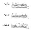
- Figs. 24A to 24Care schematic views for explaining the method of cutting a semiconductor substrate in accordance with the embodiment, in which Fig. 24A shows a state where a protective film is bonded to the silicon wafer, Fig. 24B shows a state where the silicon wafer is thinned, and Fig. 24B shows a state where the protective film is irradiated with UV rays;
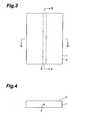
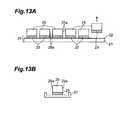
- Fig. 1is a plan view of a semiconductor substrate 1 during laser processing.
- Fig. 2is a sectional view of the semiconductor substrate I taken along the line II-II of Fig. 1.
- Fig. 3is a plan view of the semiconductor substrate 1 after the laser processing.
- Fig. 4is a sectional view of the semiconductor substrate I taken along the line IV-IV of Fig. 3.
- Fig. 5is a sectional view of the semiconductor substrate 1 taken along the line V-V of Fig. 3.
- Fig. 6is a plan view of the cut semiconductor substrate 1.
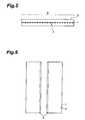
- Fig. 10is a flowchart for explaining the procedure by which thus configured laser processing apparatus 100 forms a part which is intended to be cut.
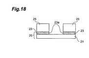
- the die-bonding resin layer 23is not left on the base 21 of the adhesive sheet 20 between the semiconductor chips 25, 25 separated from each other as shown in Fig. 18. Consequently, the cut section 25a of the semiconductor chip 25 and the cut section 23a of the die-bonding resin layer 23 in close contact with the rear face thereof can substantially coincide with each other.
Landscapes
- Engineering & Computer Science (AREA)
- Physics & Mathematics (AREA)
- Power Engineering (AREA)
- Computer Hardware Design (AREA)
- Microelectronics & Electronic Packaging (AREA)
- Manufacturing & Machinery (AREA)
- Optics & Photonics (AREA)
- General Physics & Mathematics (AREA)
- Condensed Matter Physics & Semiconductors (AREA)
- Mechanical Engineering (AREA)
- Plasma & Fusion (AREA)
- High Energy & Nuclear Physics (AREA)
- Mining & Mineral Resources (AREA)
- Chemical & Material Sciences (AREA)
- Chemical Kinetics & Catalysis (AREA)
- General Chemical & Material Sciences (AREA)
- Oil, Petroleum & Natural Gas (AREA)
- Toxicology (AREA)
- Health & Medical Sciences (AREA)
- Laser Beam Processing (AREA)
- Dicing (AREA)
- Processing Of Stones Or Stones Resemblance Materials (AREA)
Abstract
Description
The fact that the molten processed
When a cutting start region is formed as follows while taking accountof the crystal structure of a semiconductor substrate, its cleavage characteristic,and the like, the object can be cut with a high precision by a smaller forcefrom the cutting start region acting as a start point.
In the following, a preferred second embodiment of the method ofcutting a semiconductor substrate in accordance with the present inventionwill be explained more specifically. Figs. 24 to 27 are partly sectional viewsof the silicon wafer taken along the line XIII-XIII of Fig. 23.
Claims (18)
- A method of cutting a semiconductor substrate, the methodcomprising the steps ofirradiating a semiconductor substrate having a sheet bonded thereto byway of a die-bonding resin layer with laser light while locating a light-convergingpoint within the semiconductor substrate, so as to form a modifiedregion caused by multiphoton absorption within the semiconductor substrate,and causing the modified region to form a part which is intended to be cut; andexpanding the sheet after the step of forming the part which isintended to be cut, so as to cut the semiconductor substrate and die-bondingresin layer along the part which is intended to be cut.
- A method of cutting a semiconductor substrate, the methodcomprising the steps of:irradiating a semiconductor substrate having a sheet bonded thereto byway of a die-bonding resin layer with laser light while locating a light-convergingpoint within the semiconductor substrate under a condition with apeak power density of at least 1 x 10⁸ (W/cm2) at the light-converging pointand a pulse width of 1 µs or less, so as to form a modified region including amolten processed region within the semiconductor substrate, and causing themodified region including the molten processed region to form a part which isintended to be cut; andexpanding the sheet after the step of forming the part which isintended to be cut, so as to cut the semiconductor substrate and die-bondingresin layer along the part which is intended to be cut.
- A method of cutting a semiconductor substrate, the methodcomprising the steps of:irradiating a semiconductor substrate having a sheet bonded thereto byway of a die-bonding resin layer with laser light while locating a light-convergingpoint within the semiconductor substrate, so as to form a modifiedregion within the semiconductor substrate, and causing the modified region toform a part which is intended to be cut; andexpanding the sheet after the step of forming the part which isintended to be cut, so as to cut the semiconductor substrate and die-bondingresin layer along the part which is intended to be cut.
- A method of cutting a semiconductor substrate, the methodcomprising the steps of:irradiating a semiconductor substrate having a sheet bonded theretowith laser light while locating a light-converging point within thesemiconductor substrate, so as to form a modified region within thesemiconductor substrate, and causing the modified region to form a part whichis intended to be cut; andexpanding the sheet after the step of forming the part which isintended to be cut, so as to cut the semiconductor substrate along the partwhich is intended to be cut.
- A method of cutting a semiconductor substrate according to claim 3or 4, wherein the modified region is a molten processed region.
- A method of cutting a semiconductor substrate according to one ofclaims 1 to 4, wherein a fracture is caused to reach a front face of thesemiconductor substrate on the laser light entrance side from the part which isintended to be cut acting as a start point.
- A method of cutting a semiconductor substrate according to one ofclaims 1 to 4, wherein a fracture is caused to reach a rear face of the semiconductor substrate on the side opposite from the laser light entrance sidefrom the part which is intended to be cut acting as a start point.
- A method of cutting a semiconductor substrate according to one ofclaims 1 to 4, wherein a fracture is caused to reach a front face of thesemiconductor substrate on the laser light entrance side and a rear face on theside opposite therefrom from the part which is intended to be cut acting as astart point.
- A method of cutting a semiconductor substrate, the methodcomprising the steps of:irradiating a semiconductor substrate having a sheet bonded thereto byway of a die-bonding resin layer with laser light while locating a light-convergingpoint within the semiconductor substrate, so as to form a modifiedregion caused by multiphoton absorption within the semiconductor substrate,and causing the modified region to form a part which is intended to be cut;generating a stress in the semiconductor substrate along the part whichis intended to be cut after the step of forming the part which is intended to becut, so as to cut the semiconductor substrate along the part which is intendedto be cut; andexpanding the sheet after the step of cutting the semiconductorsubstrate, so as to cut the die-bonding resin layer along a cut section of thesemiconductor substrate.
- A method of cutting a semiconductor substrate, the methodcomprising the steps of:irradiating a semiconductor substrate having a sheet bonded thereto byway of a die-bonding resin layer with laser light while locating a light-convergingpoint within the semiconductor substrate under a condition with a peak power density of at least 1 x 10⁸ (W/cm2) at the light-converging pointand a pulse width of 1 µs or less, so as to form a modified region caused bymultiphoton absorption within the semiconductor substrate, and causing themodified region to form a part which is intended to be cut;generating a stress in the semiconductor substrate along the part whichis intended to be cut after the step of forming the part which is intended to becut, so as to cut the semiconductor substrate along the part which is intendedto be cut; andexpanding the sheet after the step of cutting the semiconductorsubstrate, so as to cut the die-bonding resin layer along a cut section of thesemiconductor substrate.
- A method of cutting a semiconductor substrate, the methodcomprising the steps of:irradiating a semiconductor substrate having a sheet bonded thereto byway of a die-bonding resin layer with laser light while locating a light-convergingpoint within the semiconductor substrate, so as to form a modifiedregion within the semiconductor substrate, and causing the modified region toform a part which is intended to be cut;generating a stress in the semiconductor substrate along the part whichis intended to be cut after the step of forming the part which is intended to becut, so as to cut the semiconductor substrate along the part which is intendedto be cut; andexpanding the sheet after the step of cutting the semiconductorsubstrate, so as to cut the die-bonding resin layer along a cut section of thesemiconductor substrate.
- A method of cutting a semiconductor substrate according to claim 11,
wherein the modified region is a molten processed region. - A method of cutting a semiconductor substrate having a front faceformed with a functional device along a line to cut, the method comprising thesteps of:irradiating the semiconductor substrate with laser light while using arear face of the semiconductor substrate as a laser light entrance surface andlocating a light-converging point within the semiconductor substrate, so as toform a modified region, and causing the modified region to form a cutting startregion within the semiconductor substrate inside of the laser light entrancesurface by a predetermined distance along the line to cut;attaching an expandable holding member to the rear face of thesemiconductor substrate by way of a die-bonding resin layer after forming thecutting start region; andexpanding the holding member after attaching the holding member,so as to cut the semiconductor substrate and die-bonding resin layer along theline to cut.
- A method of cutting a semiconductor substrate according to claim 13,further comprising the step of grinding the rear face of the semiconductorsubstrate such that the semiconductor substrate attains a predeterminedthickness before forming the cutting start region.
- A method of cutting a semiconductor substrate according to claim 13or 14, wherein the modified region includes a molten processed region.
- A method of cutting a semiconductor substrate according to one ofclaims 13 to 15, wherein a fracture is caused to reach the front face of thesemiconductor substrate from the cutting start region acting as a start pointwhen forming the cutting start region.
- A method of cutting a semiconductor substrate according to one ofclaims 13 to 15, wherein a fracture is caused to reach the rear face of thesemiconductor substrate from the cutting start region acting as a start pointwhen forming the cutting start region.
- A method of cutting a semiconductor substrate according to one ofclaims 13 to 15, wherein a fracture is caused to reach the front and rear facesof the semiconductor substrate from the cutting start region acting as a startpoint when forming the cutting start region.
Priority Applications (6)
| Application Number | Priority Date | Filing Date | Title |
|---|---|---|---|
| EP12001098.8AEP2485251B1 (en) | 2002-12-03 | 2003-09-11 | Method of cutting semiconductor substrate |
| EP10009049.7AEP2249380B1 (en) | 2002-12-03 | 2003-09-11 | Method for cutting semiconductor substrate |
| EP10007917.7AEP2239764B1 (en) | 2002-12-03 | 2003-09-11 | Method for cutting semiconductor substrate |
| EP10005697.7AEP2216805B1 (en) | 2002-12-03 | 2003-09-11 | Method of cutting semiconductor substrate |
| EP10012640.8AEP2267763B1 (en) | 2002-12-03 | 2003-09-11 | Method for cutting semiconductor substrate |
| EP10014153.0AEP2284872B1 (en) | 2002-12-03 | 2003-09-11 | Method for cutting semiconductor substrate |
Applications Claiming Priority (3)
| Application Number | Priority Date | Filing Date | Title |
|---|---|---|---|
| JP2002351600AJP4358502B2 (en) | 2002-03-12 | 2002-12-03 | Semiconductor substrate cutting method |
| JP2002351600 | 2002-12-03 | ||
| PCT/JP2003/011624WO2004051721A1 (en) | 2002-12-03 | 2003-09-11 | Method for cutting semiconductor substrate |
Related Child Applications (9)
| Application Number | Title | Priority Date | Filing Date |
|---|---|---|---|
| EP10009049.7ADivision-IntoEP2249380B1 (en) | 2002-12-03 | 2003-09-11 | Method for cutting semiconductor substrate |
| EP10007917.7ADivision-IntoEP2239764B1 (en) | 2002-12-03 | 2003-09-11 | Method for cutting semiconductor substrate |
| EP10005697.7ADivisionEP2216805B1 (en) | 2002-12-03 | 2003-09-11 | Method of cutting semiconductor substrate |
| EP10005697.7ADivision-IntoEP2216805B1 (en) | 2002-12-03 | 2003-09-11 | Method of cutting semiconductor substrate |
| EP12001098.8ADivision-IntoEP2485251B1 (en) | 2002-12-03 | 2003-09-11 | Method of cutting semiconductor substrate |
| EP12001098.8ADivisionEP2485251B1 (en) | 2002-12-03 | 2003-09-11 | Method of cutting semiconductor substrate |
| EP10014153.0ADivision-IntoEP2284872B1 (en) | 2002-12-03 | 2003-09-11 | Method for cutting semiconductor substrate |
| EP10012640.8ADivisionEP2267763B1 (en) | 2002-12-03 | 2003-09-11 | Method for cutting semiconductor substrate |
| EP10012640.8ADivision-IntoEP2267763B1 (en) | 2002-12-03 | 2003-09-11 | Method for cutting semiconductor substrate |
Publications (3)
| Publication Number | Publication Date |
|---|---|
| EP1580800A1true EP1580800A1 (en) | 2005-09-28 |
| EP1580800A4 EP1580800A4 (en) | 2009-09-16 |
| EP1580800B1 EP1580800B1 (en) | 2014-06-04 |
Family
ID=32463160
Family Applications (7)
| Application Number | Title | Priority Date | Filing Date |
|---|---|---|---|
| EP10009049.7AExpired - LifetimeEP2249380B1 (en) | 2002-12-03 | 2003-09-11 | Method for cutting semiconductor substrate |
| EP12001098.8AExpired - LifetimeEP2485251B1 (en) | 2002-12-03 | 2003-09-11 | Method of cutting semiconductor substrate |
| EP10007917.7AExpired - LifetimeEP2239764B1 (en) | 2002-12-03 | 2003-09-11 | Method for cutting semiconductor substrate |
| EP10012640.8AExpired - LifetimeEP2267763B1 (en) | 2002-12-03 | 2003-09-11 | Method for cutting semiconductor substrate |
| EP10005697.7AExpired - LifetimeEP2216805B1 (en) | 2002-12-03 | 2003-09-11 | Method of cutting semiconductor substrate |
| EP10014153.0AExpired - LifetimeEP2284872B1 (en) | 2002-12-03 | 2003-09-11 | Method for cutting semiconductor substrate |
| EP03812274.3AExpired - LifetimeEP1580800B1 (en) | 2002-12-03 | 2003-09-11 | Method for cutting semiconductor substrate |
Family Applications Before (6)
| Application Number | Title | Priority Date | Filing Date |
|---|---|---|---|
| EP10009049.7AExpired - LifetimeEP2249380B1 (en) | 2002-12-03 | 2003-09-11 | Method for cutting semiconductor substrate |
| EP12001098.8AExpired - LifetimeEP2485251B1 (en) | 2002-12-03 | 2003-09-11 | Method of cutting semiconductor substrate |
| EP10007917.7AExpired - LifetimeEP2239764B1 (en) | 2002-12-03 | 2003-09-11 | Method for cutting semiconductor substrate |
| EP10012640.8AExpired - LifetimeEP2267763B1 (en) | 2002-12-03 | 2003-09-11 | Method for cutting semiconductor substrate |
| EP10005697.7AExpired - LifetimeEP2216805B1 (en) | 2002-12-03 | 2003-09-11 | Method of cutting semiconductor substrate |
| EP10014153.0AExpired - LifetimeEP2284872B1 (en) | 2002-12-03 | 2003-09-11 | Method for cutting semiconductor substrate |
Country Status (9)
| Country | Link |
|---|---|
| US (4) | US8263479B2 (en) |
| EP (7) | EP2249380B1 (en) |
| KR (1) | KR100855136B1 (en) |
| CN (2) | CN101369554A (en) |
| AU (1) | AU2003262077A1 (en) |
| ES (7) | ES2462219T3 (en) |
| MY (1) | MY160196A (en) |
| TW (1) | TWI520269B (en) |
| WO (1) | WO2004051721A1 (en) |
Cited By (14)
| Publication number | Priority date | Publication date | Assignee | Title |
|---|---|---|---|---|
| NL1029172C2 (en)* | 2005-06-02 | 2006-12-05 | Fico Bv | Method and device for cutting electronic components with a laser beam. |
| EP1610364A4 (en)* | 2003-03-12 | 2008-08-27 | Hamamatsu Photonics Kk | Laser beam machining method |
| EP1983557A4 (en)* | 2005-12-27 | 2009-04-22 | Hamamatsu Photonics Kk | LASER BEAM MACHINING PROCESS AND SEMICONDUCTOR CHIP |
| EP1906438A4 (en)* | 2005-07-04 | 2009-04-22 | Hamamatsu Photonics Kk | METHOD OF CUTTING PIECE |
| US7547613B2 (en) | 2000-09-13 | 2009-06-16 | Hamamatsu Photonics K.K. | Laser processing method and laser processing apparatus |
| US7566635B2 (en) | 2002-03-12 | 2009-07-28 | Hamamatsu Photonics K.K. | Substrate dividing method |
| US7749867B2 (en) | 2002-03-12 | 2010-07-06 | Hamamatsu Photonics K.K. | Method of cutting processed object |
| US7981770B2 (en) | 2006-03-03 | 2011-07-19 | Tokyo Seimitsu Co., Ltd. | Wafer machining method for preparing a wafer for dicing |
| DE102010009015A1 (en)* | 2010-02-24 | 2011-08-25 | OSRAM Opto Semiconductors GmbH, 93055 | Method for producing a plurality of optoelectronic semiconductor chips |
| DE102005004845B4 (en)* | 2004-02-03 | 2012-01-26 | Disco Corp. | Wafer dividing method |
| US8247734B2 (en) | 2003-03-11 | 2012-08-21 | Hamamatsu Photonics K.K. | Laser beam machining method |
| US8263479B2 (en) | 2002-12-03 | 2012-09-11 | Hamamatsu Photonics K.K. | Method for cutting semiconductor substrate |
| US8685838B2 (en) | 2003-03-12 | 2014-04-01 | Hamamatsu Photonics K.K. | Laser beam machining method |
| US8735771B2 (en) | 2005-03-22 | 2014-05-27 | Hamamatsu Photonicks K.K. | Laser machining method |
Families Citing this family (101)
| Publication number | Priority date | Publication date | Assignee | Title |
|---|---|---|---|---|
| JP2005032903A (en)* | 2003-07-10 | 2005-02-03 | Oki Electric Ind Co Ltd | Semiconductor device and manufacturing method thereof |
| CN101862907B (en)* | 2003-07-18 | 2014-01-22 | 浜松光子学株式会社 | Laser beam machining method, laser beam machining apparatus, and laser machined product |
| JP4563097B2 (en)* | 2003-09-10 | 2010-10-13 | 浜松ホトニクス株式会社 | Semiconductor substrate cutting method |
| JP4509578B2 (en) | 2004-01-09 | 2010-07-21 | 浜松ホトニクス株式会社 | Laser processing method and laser processing apparatus |
| JP4598407B2 (en)* | 2004-01-09 | 2010-12-15 | 浜松ホトニクス株式会社 | Laser processing method and laser processing apparatus |
| JP4601965B2 (en)* | 2004-01-09 | 2010-12-22 | 浜松ホトニクス株式会社 | Laser processing method and laser processing apparatus |
| EP1742253B1 (en)* | 2004-03-30 | 2012-05-09 | Hamamatsu Photonics K.K. | Laser processing method |
| KR101109860B1 (en)* | 2004-08-06 | 2012-02-21 | 하마마츠 포토닉스 가부시키가이샤 | Laser processing method, cutting method for work and semiconductor device |
| JP2007081037A (en)* | 2005-09-13 | 2007-03-29 | Disco Abrasive Syst Ltd | Device and manufacturing method thereof |
| JP4762653B2 (en)* | 2005-09-16 | 2011-08-31 | 浜松ホトニクス株式会社 | Laser processing method and laser processing apparatus |
| JP4830740B2 (en)* | 2005-11-16 | 2011-12-07 | 株式会社デンソー | Manufacturing method of semiconductor chip |
| US20070111480A1 (en)* | 2005-11-16 | 2007-05-17 | Denso Corporation | Wafer product and processing method therefor |
| JP4237745B2 (en) | 2005-11-18 | 2009-03-11 | 浜松ホトニクス株式会社 | Laser processing method |
| JP4907965B2 (en)* | 2005-11-25 | 2012-04-04 | 浜松ホトニクス株式会社 | Laser processing method |
| JP4804911B2 (en)* | 2005-12-22 | 2011-11-02 | 浜松ホトニクス株式会社 | Laser processing equipment |
| JP2007266557A (en)* | 2006-03-30 | 2007-10-11 | Renesas Technology Corp | Method of manufacturing semiconductor device |
| EP1875983B1 (en)* | 2006-07-03 | 2013-09-11 | Hamamatsu Photonics K.K. | Laser processing method and chip |
| JP5183892B2 (en) | 2006-07-03 | 2013-04-17 | 浜松ホトニクス株式会社 | Laser processing method |
| JP4954653B2 (en) | 2006-09-19 | 2012-06-20 | 浜松ホトニクス株式会社 | Laser processing method |
| CN101516566B (en)* | 2006-09-19 | 2012-05-09 | 浜松光子学株式会社 | Laser processing method and laser processing apparatus |
| JP5101073B2 (en)* | 2006-10-02 | 2012-12-19 | 浜松ホトニクス株式会社 | Laser processing equipment |
| JP5132911B2 (en)* | 2006-10-03 | 2013-01-30 | 浜松ホトニクス株式会社 | Laser processing method |
| JP4964554B2 (en)* | 2006-10-03 | 2012-07-04 | 浜松ホトニクス株式会社 | Laser processing method |
| WO2008041604A1 (en)* | 2006-10-04 | 2008-04-10 | Hamamatsu Photonics K.K. | Laser processing method |
| US20080206897A1 (en)* | 2007-02-27 | 2008-08-28 | Woo Sik Yoo | Selective Depth Optical Processing |
| DE202007004412U1 (en)* | 2007-03-22 | 2008-07-24 | STABILA Messgeräte Gustav Ullrich GmbH | spirit level |
| US20080232419A1 (en)* | 2007-03-22 | 2008-09-25 | Seiko Epson Corporation | Laser array chip, laser module, manufacturing method for manufacturing laser module, manufacturing method for manufacturing laser light source, laser light source, illumination device, monitor, and projector |
| JP5336054B2 (en) | 2007-07-18 | 2013-11-06 | 浜松ホトニクス株式会社 | Processing information supply system provided with processing information supply device |
| JP5267462B2 (en)* | 2007-08-03 | 2013-08-21 | 日亜化学工業株式会社 | Semiconductor light emitting device and manufacturing method thereof |
| JP5449665B2 (en)* | 2007-10-30 | 2014-03-19 | 浜松ホトニクス株式会社 | Laser processing method |
| JP5134928B2 (en)* | 2007-11-30 | 2013-01-30 | 浜松ホトニクス株式会社 | Workpiece grinding method |
| JP5054496B2 (en)* | 2007-11-30 | 2012-10-24 | 浜松ホトニクス株式会社 | Processing object cutting method |
| JP5692969B2 (en) | 2008-09-01 | 2015-04-01 | 浜松ホトニクス株式会社 | Aberration correction method, laser processing method using this aberration correction method, laser irradiation method using this aberration correction method, aberration correction apparatus, and aberration correction program |
| JP5254761B2 (en) | 2008-11-28 | 2013-08-07 | 浜松ホトニクス株式会社 | Laser processing equipment |
| JP5241525B2 (en) | 2009-01-09 | 2013-07-17 | 浜松ホトニクス株式会社 | Laser processing equipment |
| JP5241527B2 (en) | 2009-01-09 | 2013-07-17 | 浜松ホトニクス株式会社 | Laser processing equipment |
| KR101757937B1 (en) | 2009-02-09 | 2017-07-13 | 하마마츠 포토닉스 가부시키가이샤 | Workpiece cutting method |
| EP2402984B1 (en) | 2009-02-25 | 2018-01-10 | Nichia Corporation | Method of manufacturing a semiconductor element, and corresponding semicondutor element |
| JP5639997B2 (en) | 2009-04-07 | 2014-12-10 | 浜松ホトニクス株式会社 | Laser processing equipment |
| JP5491761B2 (en) | 2009-04-20 | 2014-05-14 | 浜松ホトニクス株式会社 | Laser processing equipment |
| JP5476063B2 (en) | 2009-07-28 | 2014-04-23 | 浜松ホトニクス株式会社 | Processing object cutting method |
| JP5537081B2 (en) | 2009-07-28 | 2014-07-02 | 浜松ホトニクス株式会社 | Processing object cutting method |
| US20120061356A1 (en)* | 2009-08-11 | 2012-03-15 | Hamamatsu Photonics K.K. | Laser machining device and laser machining method |
| JP5379604B2 (en) | 2009-08-21 | 2013-12-25 | 浜松ホトニクス株式会社 | Laser processing method and chip |
| JP2011060848A (en)* | 2009-09-07 | 2011-03-24 | Nitto Denko Corp | Thermosetting type die bond film, dicing-die bond film and semiconductor device |
| EP2511942A1 (en)* | 2009-12-11 | 2012-10-17 | Sharp Kabushiki Kaisha | Method for manufacturing semiconductor device, and semiconductor device |
| JP5583981B2 (en)* | 2010-01-25 | 2014-09-03 | 株式会社ディスコ | Laser processing method |
| JP5670647B2 (en) | 2010-05-14 | 2015-02-18 | 浜松ホトニクス株式会社 | Processing object cutting method |
| US8950217B2 (en) | 2010-05-14 | 2015-02-10 | Hamamatsu Photonics K.K. | Method of cutting object to be processed, method of cutting strengthened glass sheet and method of manufacturing strengthened glass member |
| JP2012000636A (en) | 2010-06-16 | 2012-01-05 | Showa Denko Kk | Laser beam machining method |
| KR20130106770A (en)* | 2010-07-26 | 2013-09-30 | 하마마츠 포토닉스 가부시키가이샤 | Method for manufacturing semiconductor device |
| US8722516B2 (en) | 2010-09-28 | 2014-05-13 | Hamamatsu Photonics K.K. | Laser processing method and method for manufacturing light-emitting device |
| JP2012079936A (en) | 2010-10-01 | 2012-04-19 | Nitto Denko Corp | Dicing, die-bonding film and method for manufacturing semiconductor device |
| JP5480169B2 (en) | 2011-01-13 | 2014-04-23 | 浜松ホトニクス株式会社 | Laser processing method |
| US8538576B2 (en)* | 2011-04-05 | 2013-09-17 | Asm Technology Singapore Pte. Ltd. | Method of configuring a dicing device, and a dicing apparatus for dicing a workpiece |
| JP2012238746A (en)* | 2011-05-12 | 2012-12-06 | Disco Abrasive Syst Ltd | Division method of optical device wafer |
| KR101800223B1 (en)* | 2011-06-08 | 2017-11-22 | 니폰 덴키 가라스 가부시키가이샤 | Method for cutting plate-like glass, and cutting device therefor |
| JP2013008915A (en)* | 2011-06-27 | 2013-01-10 | Toshiba Corp | Substrate processing method and substrate processing apparatus |
| US9293690B2 (en)* | 2011-06-27 | 2016-03-22 | Koninklijke Philips N.V. | Ultrasound transducer assembly and method of manufacturing the same |
| US8697463B2 (en)* | 2012-01-26 | 2014-04-15 | Epistar Corporation | Manufacturing method of a light-emitting device |
| JP5919087B2 (en)* | 2012-05-10 | 2016-05-18 | ルネサスエレクトロニクス株式会社 | Semiconductor device manufacturing method and semiconductor device |
| JP2013237097A (en)* | 2012-05-17 | 2013-11-28 | Disco Corp | Modified layer forming method |
| JP2014179419A (en)* | 2013-03-14 | 2014-09-25 | Alpha- Design Kk | Method for bonding electronic component |
| US9640714B2 (en) | 2013-08-29 | 2017-05-02 | Nichia Corporation | Method for manufacturing light emitting element |
| US8993412B1 (en)* | 2013-12-05 | 2015-03-31 | Texas Instruments Incorporated | Method for reducing backside die damage during die separation process |
| US9859162B2 (en) | 2014-09-11 | 2018-01-02 | Alta Devices, Inc. | Perforation of films for separation |
| JP6347714B2 (en)* | 2014-10-02 | 2018-06-27 | 株式会社ディスコ | Wafer processing method |
| JP6395613B2 (en)* | 2015-01-06 | 2018-09-26 | 株式会社ディスコ | Wafer generation method |
| JP6395633B2 (en) | 2015-02-09 | 2018-09-26 | 株式会社ディスコ | Wafer generation method |
| JP6395632B2 (en) | 2015-02-09 | 2018-09-26 | 株式会社ディスコ | Wafer generation method |
| JP2016167552A (en)* | 2015-03-10 | 2016-09-15 | 株式会社ディスコ | Single crystal substrate processing method |
| JP6429715B2 (en) | 2015-04-06 | 2018-11-28 | 株式会社ディスコ | Wafer generation method |
| JP6425606B2 (en) | 2015-04-06 | 2018-11-21 | 株式会社ディスコ | Wafer production method |
| JP6494382B2 (en)* | 2015-04-06 | 2019-04-03 | 株式会社ディスコ | Wafer generation method |
| JP6472333B2 (en) | 2015-06-02 | 2019-02-20 | 株式会社ディスコ | Wafer generation method |
| JP6482423B2 (en) | 2015-07-16 | 2019-03-13 | 株式会社ディスコ | Wafer generation method |
| JP6472347B2 (en) | 2015-07-21 | 2019-02-20 | 株式会社ディスコ | Thinning method of wafer |
| JP6482425B2 (en) | 2015-07-21 | 2019-03-13 | 株式会社ディスコ | Thinning method of wafer |
| JP6594699B2 (en)* | 2015-08-18 | 2019-10-23 | 浜松ホトニクス株式会社 | Processing object cutting method and processing object cutting apparatus |
| CN108140609B (en)* | 2015-08-31 | 2022-10-11 | 株式会社迪思科 | Method for processing wafer and protective sheet used in the method |
| KR102546307B1 (en) | 2015-12-02 | 2023-06-21 | 삼성전자주식회사 | Light emitting device and display device including the same |
| JP6690983B2 (en) | 2016-04-11 | 2020-04-28 | 株式会社ディスコ | Wafer generation method and actual second orientation flat detection method |
| CN107579041A (en)* | 2016-07-05 | 2018-01-12 | 力成科技股份有限公司 | Manufacturing method of packaging structure |
| JP2018042208A (en)* | 2016-09-09 | 2018-03-15 | 株式会社ディスコ | Manufacturing method for surface elastic wave device chip |
| JP6821245B2 (en)* | 2016-10-11 | 2021-01-27 | 株式会社ディスコ | Wafer processing method |
| JP6858587B2 (en) | 2017-02-16 | 2021-04-14 | 株式会社ディスコ | Wafer generation method |
| JP2018160623A (en)* | 2017-03-23 | 2018-10-11 | 東芝メモリ株式会社 | Manufacturing method of semiconductor device |
| TWI606530B (en)* | 2017-03-29 | 2017-11-21 | 台灣愛司帝科技股份有限公司 | Position detection and wafer separation device |
| JP6991475B2 (en)* | 2017-05-24 | 2022-01-12 | 協立化学産業株式会社 | How to cut the object to be processed |
| JP6855127B2 (en)* | 2017-06-05 | 2021-04-07 | 株式会社ディスコ | Chip manufacturing method |
| KR102563724B1 (en) | 2017-11-29 | 2023-08-07 | 니치아 카가쿠 고교 가부시키가이샤 | Manufacturing method of semiconductor light emitting device |
| CN108214593B (en)* | 2018-01-02 | 2019-11-29 | 京东方科技集团股份有限公司 | A kind of break bar, cutter device and cutting method |
| DE102018115205A1 (en)* | 2018-06-25 | 2020-01-02 | Vishay Electronic Gmbh | Process for manufacturing a large number of resistance units |
| US10576585B1 (en) | 2018-12-29 | 2020-03-03 | Cree, Inc. | Laser-assisted method for parting crystalline material |
| US10562130B1 (en) | 2018-12-29 | 2020-02-18 | Cree, Inc. | Laser-assisted method for parting crystalline material |
| US11024501B2 (en) | 2018-12-29 | 2021-06-01 | Cree, Inc. | Carrier-assisted method for parting crystalline material along laser damage region |
| US10611052B1 (en) | 2019-05-17 | 2020-04-07 | Cree, Inc. | Silicon carbide wafers with relaxed positive bow and related methods |
| JP7370881B2 (en)* | 2020-01-24 | 2023-10-30 | 株式会社ディスコ | Wafer processing method and wafer processing equipment |
| JP7599795B2 (en)* | 2021-04-13 | 2024-12-16 | 株式会社ディスコ | Resin coating method and resin coating device |
| CN113964170A (en)* | 2021-11-22 | 2022-01-21 | 福建华佳彩有限公司 | Substrate structure capable of improving cutting yield |
| US20230207390A1 (en)* | 2021-12-23 | 2023-06-29 | Texas Instruments Incorporated | Method of controlled propagation of laser induced silicon cracks through a balanced compressive and retractive cyclical force for laser dicing |
Family Cites Families (332)
| Publication number | Priority date | Publication date | Assignee | Title |
|---|---|---|---|---|
| US3448510A (en) | 1966-05-20 | 1969-06-10 | Western Electric Co | Methods and apparatus for separating articles initially in a compact array,and composite assemblies so formed |
| DE1964332U (en) | 1967-02-27 | 1967-07-20 | Segger & Soehne B | CARRYING CONTAINER FOR INDUSTRIAL EQUIPMENT. |
| JPS4624989Y1 (en) | 1967-08-31 | 1971-08-28 | ||
| US3629545A (en) | 1967-12-19 | 1971-12-21 | Western Electric Co | Laser substrate parting |
| GB1246481A (en) | 1968-03-29 | 1971-09-15 | Pilkington Brothers Ltd | Improvements in or relating to the cutting of glass |
| US3613974A (en) | 1969-03-10 | 1971-10-19 | Saint Gobain | Apparatus for cutting glass |
| JPS4812599Y1 (en) | 1969-03-24 | 1973-04-05 | ||
| US3610871A (en) | 1970-02-19 | 1971-10-05 | Western Electric Co | Initiation of a controlled fracture |
| US3626141A (en) | 1970-04-30 | 1971-12-07 | Quantronix Corp | Laser scribing apparatus |
| US3824678A (en) | 1970-08-31 | 1974-07-23 | North American Rockwell | Process for laser scribing beam lead semiconductor wafers |
| US3790744A (en) | 1971-07-19 | 1974-02-05 | American Can Co | Method of forming a line of weakness in a multilayer laminate |
| US3909582A (en) | 1971-07-19 | 1975-09-30 | American Can Co | Method of forming a line of weakness in a multilayer laminate |
| US3790051A (en) | 1971-09-07 | 1974-02-05 | Radiant Energy Systems | Semiconductor wafer fracturing technique employing a pressure controlled roller |
| US3970819A (en) | 1974-11-25 | 1976-07-20 | International Business Machines Corporation | Backside laser dicing system |
| JPS5333050A (en) | 1976-09-08 | 1978-03-28 | Hitachi Ltd | Production of semiconductor element |
| US4092518A (en) | 1976-12-07 | 1978-05-30 | Laser Technique S.A. | Method of decorating a transparent plastics material article by means of a laser beam |
| JPS53141573A (en) | 1977-05-16 | 1978-12-09 | Toshiba Corp | Pellet dividing method of semiconductor wafer |
| US4242152A (en) | 1979-05-14 | 1980-12-30 | National Semiconductor Corporation | Method for adjusting the focus and power of a trimming laser |
| JPS5628630A (en) | 1979-08-16 | 1981-03-20 | Kawasaki Steel Corp | Temperature controlling method of high temperature high pressure reacting cylinder |
| JPS6041478B2 (en) | 1979-09-10 | 1985-09-17 | 富士通株式会社 | Manufacturing method of semiconductor laser device |
| JPS5676522A (en) | 1979-11-29 | 1981-06-24 | Toshiba Corp | Formation of semiconductor thin film |
| JPS6043236B2 (en) | 1980-03-12 | 1985-09-27 | 松下電器産業株式会社 | Laser processing method |
| US4336439A (en) | 1980-10-02 | 1982-06-22 | Coherent, Inc. | Method and apparatus for laser scribing and cutting |
| JPS5836939A (en) | 1981-08-26 | 1983-03-04 | Toshiba Corp | Cutting method for glass wafer |
| JPS5854648A (en) | 1981-09-28 | 1983-03-31 | Nippon Kogaku Kk <Nikon> | alignment device |
| JPS5857767A (en) | 1981-10-01 | 1983-04-06 | Matsushita Electric Ind Co Ltd | Laser device |
| US4475027A (en) | 1981-11-17 | 1984-10-02 | Allied Corporation | Optical beam homogenizer |
| JPS58181492A (en) | 1982-04-02 | 1983-10-24 | グレタ−ク・アクチエンゲゼルシヤフト | Method and device for focussing optical beam having coherence |
| JPS58171783A (en) | 1982-04-02 | 1983-10-08 | Hitachi Ltd | magnetic bubble memory chip |
| JPS58171783U (en) | 1982-05-14 | 1983-11-16 | 有限会社河島農具製作所 | Crawler tensioning device |
| JPS6054151B2 (en) | 1982-10-22 | 1985-11-28 | 株式会社東芝 | Laser cutting method |
| US4689467A (en) | 1982-12-17 | 1987-08-25 | Inoue-Japax Research Incorporated | Laser machining apparatus |
| JPS59141233A (en) | 1983-02-02 | 1984-08-13 | Nec Corp | Manufacture of semiconductor device |
| JPS59150691A (en) | 1983-02-15 | 1984-08-28 | Matsushita Electric Ind Co Ltd | Laser working machine |
| JPH0611071B2 (en)* | 1983-09-07 | 1994-02-09 | 三洋電機株式会社 | Method for dividing compound semiconductor substrate |
| US4546231A (en) | 1983-11-14 | 1985-10-08 | Group Ii Manufacturing Ltd. | Creation of a parting zone in a crystal structure |
| JPS59130438A (en) | 1983-11-28 | 1984-07-27 | Hitachi Ltd | Method for separating plates |
| US4650619A (en) | 1983-12-29 | 1987-03-17 | Toshiba Ceramics Co., Ltd. | Method of machining a ceramic member |
| JPS60144985A (en) | 1983-12-30 | 1985-07-31 | Fujitsu Ltd | Manufacturing method of semiconductor light emitting device |
| JPS60167351A (en) | 1984-02-09 | 1985-08-30 | Mitsubishi Electric Corp | Manufacture of hybrid integrated circuit device |
| US4562333A (en) | 1984-09-04 | 1985-12-31 | General Electric Company | Stress assisted cutting of high temperature embrittled materials |
| JPS6196439A (en) | 1984-10-17 | 1986-05-15 | Toray Ind Inc | Lens defect inspecting instrument |
| JPS61112345A (en) | 1984-11-07 | 1986-05-30 | Toshiba Corp | Manufacturing method of semiconductor device |
| JPS61121453A (en) | 1984-11-19 | 1986-06-09 | Matsushita Electric Ind Co Ltd | Breaking and expanding method of brittle thin plate |
| JPS61220339A (en) | 1985-03-26 | 1986-09-30 | Nippon Telegr & Teleph Corp <Ntt> | Control of characteristics of semiconductor material |
| JPS61229487A (en) | 1985-04-03 | 1986-10-13 | Sasaki Glass Kk | Method for cutting glass by laser beam |
| JPS624341A (en) | 1985-06-29 | 1987-01-10 | Toshiba Corp | Manufacture of semiconductor device |
| JPS6240986A (en) | 1985-08-20 | 1987-02-21 | Fuji Electric Corp Res & Dev Ltd | Laser processing method |
| JPH0732281B2 (en) | 1985-10-25 | 1995-04-10 | 株式会社日立製作所 | Cleaving device and cleaving method |
| AU584563B2 (en) | 1986-01-31 | 1989-05-25 | Ciba-Geigy Ag | Laser marking of ceramic materials, glazes, glass ceramics and glasses |
| US4691093A (en) | 1986-04-22 | 1987-09-01 | United Technologies Corporation | Twin spot laser welding |
| FR2605310B1 (en) | 1986-10-16 | 1992-04-30 | Comp Generale Electricite | METHOD FOR REINFORCING CERAMIC WORKPIECES BY LASER TREATMENT |
| US4815854A (en) | 1987-01-19 | 1989-03-28 | Nec Corporation | Method of alignment between mask and semiconductor wafer |
| JPH0688149B2 (en) | 1987-03-04 | 1994-11-09 | 株式会社半導体エネルギ−研究所 | Light processing method |
| JPS63278692A (en) | 1987-05-07 | 1988-11-16 | D S Sukiyanaa:Kk | Automatic focusing mechanism in laser beam machine |
| JPS6438209A (en) | 1987-08-04 | 1989-02-08 | Nec Corp | Preparation of semiconductor device |
| JPH01112130A (en) | 1987-10-26 | 1989-04-28 | Matsushita Electric Ind Co Ltd | Evaluation method of infrared optical fiber |
| US4981525A (en) | 1988-02-19 | 1991-01-01 | Sanyo Electric Co., Ltd. | Photovoltaic device |
| JPH0256987A (en) | 1988-02-23 | 1990-02-26 | Mitsubishi Electric Corp | How to implement hybrid integrated circuits |
| JPH01225509A (en) | 1988-03-04 | 1989-09-08 | Sumitomo Electric Ind Ltd | Dividing method for semiconductor base |
| JPH01225510A (en) | 1988-03-04 | 1989-09-08 | Sumitomo Electric Ind Ltd | How to cut and divide semiconductor substrates |
| JPH01133701U (en) | 1988-03-07 | 1989-09-12 | ||
| JP2680039B2 (en) | 1988-06-08 | 1997-11-19 | 株式会社日立製作所 | Optical information recording / reproducing method and recording / reproducing apparatus |
| JP2507665B2 (en) | 1989-05-09 | 1996-06-12 | 株式会社東芝 | Method for manufacturing metal cylindrical member for electron tube |
| JP2810151B2 (en) | 1989-10-07 | 1998-10-15 | ホーヤ株式会社 | Laser marking method |
| JP2765746B2 (en) | 1990-03-27 | 1998-06-18 | 科学技術振興事業団 | Fine modification and processing method |
| JP2891264B2 (en) | 1990-02-09 | 1999-05-17 | ローム 株式会社 | Method for manufacturing semiconductor device |
| US5132505A (en) | 1990-03-21 | 1992-07-21 | U.S. Philips Corporation | Method of cleaving a brittle plate and device for carrying out the method |
| JPH03276662A (en) | 1990-03-26 | 1991-12-06 | Nippon Steel Corp | Wafer cutting method |
| JP2620723B2 (en) | 1990-05-24 | 1997-06-18 | サンケン電気株式会社 | Method for manufacturing semiconductor device |
| JP3024990B2 (en) | 1990-08-31 | 2000-03-27 | 日本石英硝子株式会社 | Cutting method of quartz glass material |
| JPH04167985A (en) | 1990-10-31 | 1992-06-16 | Nagasaki Pref Gov | Method for cutting off wafer |
| FR2669427B1 (en) | 1990-11-16 | 1993-01-22 | Thomson Csf | DEVICE FOR CONTROLLING ALIGNMENT OF TWO OPTICAL CHANNELS AND LASER DESIGNATION SYSTEM PROVIDED WITH SUCH A CONTROL DEVICE. |
| JPH04188847A (en) | 1990-11-22 | 1992-07-07 | Mitsubishi Electric Corp | Adhesive tape |
| US5211805A (en)* | 1990-12-19 | 1993-05-18 | Rangaswamy Srinivasan | Cutting of organic solids by continuous wave ultraviolet irradiation |
| JPH0639572A (en) | 1991-01-11 | 1994-02-15 | Souei Tsusho Kk | Wafer cutting device |
| IL97479A (en) | 1991-03-08 | 1994-01-25 | Shafir Aaron | Laser beam heating method and apparatus |
| JPH04300084A (en) | 1991-03-28 | 1992-10-23 | Toshiba Corp | laser processing machine |
| JP3165192B2 (en) | 1991-03-28 | 2001-05-14 | 株式会社東芝 | Method for manufacturing semiconductor integrated circuit device |
| JPH04339586A (en) | 1991-05-13 | 1992-11-26 | Mitsubishi Electric Corp | Laser beam machine |
| JP3213338B2 (en) | 1991-05-15 | 2001-10-02 | 株式会社リコー | Manufacturing method of thin film semiconductor device |
| US5230184A (en) | 1991-07-05 | 1993-07-27 | Motorola, Inc. | Distributed polishing head |
| US5762744A (en) | 1991-12-27 | 1998-06-09 | Rohm Co., Ltd. | Method of producing a semiconductor device using an expand tape |
| SG52223A1 (en) | 1992-01-08 | 1998-09-28 | Murata Manufacturing Co | Component supply method |
| RU2024441C1 (en) | 1992-04-02 | 1994-12-15 | Владимир Степанович Кондратенко | Process of cutting of nonmetal materials |
| US5254149A (en) | 1992-04-06 | 1993-10-19 | Ford Motor Company | Process for determining the quality of temper of a glass sheet using a laser beam |
| JP3101421B2 (en) | 1992-05-29 | 2000-10-23 | 富士通株式会社 | Manufacturing method of shaped metal pattern |
| JP3088193B2 (en) | 1992-06-05 | 2000-09-18 | 三菱電機株式会社 | Method for manufacturing semiconductor device having LOC structure and lead frame used therein |
| GB9216643D0 (en) | 1992-08-05 | 1992-09-16 | Univ Loughborough | Automatic operations on materials |
| AU5872994A (en) | 1992-12-18 | 1994-07-19 | Firebird Traders Ltd. | Process and apparatus for etching an image within a solid article |
| JP3255741B2 (en) | 1992-12-22 | 2002-02-12 | リンテック株式会社 | Wafer dicing method, radiation irradiation apparatus used for this method, and pressure-sensitive adhesive sheet for attaching a wafer |
| JP2720744B2 (en) | 1992-12-28 | 1998-03-04 | 三菱電機株式会社 | Laser processing machine |
| US5382770A (en) | 1993-01-14 | 1995-01-17 | Reliant Laser Corporation | Mirror-based laser-processing system with visual tracking and position control of a moving laser spot |
| US5637244A (en) | 1993-05-13 | 1997-06-10 | Podarok International, Inc. | Method and apparatus for creating an image by a pulsed laser beam inside a transparent material |
| JP3293136B2 (en) | 1993-06-04 | 2002-06-17 | セイコーエプソン株式会社 | Laser processing apparatus and laser processing method |
| JPH0775955A (en)* | 1993-06-17 | 1995-03-20 | Disco Abrasive Syst Ltd | Precision cutting equipment |
| US5580473A (en) | 1993-06-21 | 1996-12-03 | Sanyo Electric Co. Ltd. | Methods of removing semiconductor film with energy beams |
| JPH0729855A (en) | 1993-07-12 | 1995-01-31 | Sumitomo Electric Ind Ltd | Method for expanding semiconductor wafer |
| JPH0732281A (en) | 1993-07-19 | 1995-02-03 | Toyoda Mach Works Ltd | Robot controller |
| JP2616247B2 (en)* | 1993-07-24 | 1997-06-04 | 日本電気株式会社 | Method for manufacturing semiconductor device |
| JPH0740336A (en) | 1993-07-30 | 1995-02-10 | Sumitomo Electric Ind Ltd | Diamond processing method |
| GB2281129B (en) | 1993-08-19 | 1997-04-09 | United Distillers Plc | Method of marking a body of glass |
| JPH0776167A (en) | 1993-09-08 | 1995-03-20 | Miyachi Technos Kk | Laser marking method |
| US5376793A (en) | 1993-09-15 | 1994-12-27 | Stress Photonics, Inc. | Forced-diffusion thermal imaging apparatus and method |
| JP2760288B2 (en) | 1993-12-28 | 1998-05-28 | 日本電気株式会社 | Via hole forming method and film cutting method |
| DE4404141A1 (en) | 1994-02-09 | 1995-08-10 | Fraunhofer Ges Forschung | Device and method for laser beam shaping, especially in laser beam surface processing |
| JPH07263382A (en) | 1994-03-24 | 1995-10-13 | Kawasaki Steel Corp | Wafer fixing tape |
| US5656186A (en) | 1994-04-08 | 1997-08-12 | The Regents Of The University Of Michigan | Method for controlling configuration of laser induced breakdown and ablation |
| US5776220A (en) | 1994-09-19 | 1998-07-07 | Corning Incorporated | Method and apparatus for breaking brittle materials |
| US5622540A (en) | 1994-09-19 | 1997-04-22 | Corning Incorporated | Method for breaking a glass sheet |
| JP3374880B2 (en) | 1994-10-26 | 2003-02-10 | 三菱電機株式会社 | Semiconductor device manufacturing method and semiconductor device |
| JP3535241B2 (en) | 1994-11-18 | 2004-06-07 | 株式会社半導体エネルギー研究所 | Semiconductor device and manufacturing method thereof |
| JPH08148692A (en) | 1994-11-24 | 1996-06-07 | Sony Corp | Manufacture of thin-film semiconductor device |
| US5543365A (en) | 1994-12-02 | 1996-08-06 | Texas Instruments Incorporated | Wafer scribe technique using laser by forming polysilicon |
| JPH08197271A (en) | 1995-01-27 | 1996-08-06 | Ricoh Co Ltd | Brittle material cleaving method and brittle material cleaving apparatus |
| US5841543A (en) | 1995-03-09 | 1998-11-24 | Texas Instruments Incorporated | Method and apparatus for verifying the presence of a material applied to a substrate |
| JPH08264488A (en) | 1995-03-22 | 1996-10-11 | Nec Corp | Wafer scribing apparatus and method |
| JP3509985B2 (en) | 1995-03-24 | 2004-03-22 | 三菱電機株式会社 | Chip separation method for semiconductor device |
| US5786560A (en) | 1995-03-31 | 1998-07-28 | Panasonic Technologies, Inc. | 3-dimensional micromachining with femtosecond laser pulses |
| JP2737744B2 (en) | 1995-04-26 | 1998-04-08 | 日本電気株式会社 | Wafer probing equipment |
| JPH09150286A (en) | 1995-06-26 | 1997-06-10 | Corning Inc | Method and apparatus for cutting brittle material |
| JPH0917756A (en)* | 1995-06-28 | 1997-01-17 | Toshiba Corp | Protective tape for semiconductor and method of using the same |
| KR970008386A (en) | 1995-07-07 | 1997-02-24 | 하라 세이지 | A method of dividing a substrate and a dividing device |
| JPH0929472A (en) | 1995-07-14 | 1997-02-04 | Hitachi Ltd | Cleaving method, cleaving device and chip material |
| KR100447786B1 (en) | 1995-08-31 | 2004-11-06 | 코닝 인코포레이티드 | Method and apparatus for brittle material cutting |
| US6057525A (en) | 1995-09-05 | 2000-05-02 | United States Enrichment Corporation | Method and apparatus for precision laser micromachining |
| US5641416A (en) | 1995-10-25 | 1997-06-24 | Micron Display Technology, Inc. | Method for particulate-free energy beam cutting of a wafer of die assemblies |
| KR0171947B1 (en) | 1995-12-08 | 1999-03-20 | 김주용 | Exposure method for manufacturing semiconductor device and exposure device using same |
| JP3592018B2 (en) | 1996-01-22 | 2004-11-24 | 日本テキサス・インスツルメンツ株式会社 | Polyimide adhesive sheet and process film for polyimide |
| MY118036A (en)* | 1996-01-22 | 2004-08-30 | Lintec Corp | Wafer dicing/bonding sheet and process for producing semiconductor device |
| JPH09213662A (en) | 1996-01-31 | 1997-08-15 | Toshiba Corp | Wafer dividing method and semiconductor device manufacturing method |
| JPH09216085A (en) | 1996-02-07 | 1997-08-19 | Canon Inc | Substrate cutting method and cutting device |
| JP3660741B2 (en) | 1996-03-22 | 2005-06-15 | 株式会社日立製作所 | Method for manufacturing electronic circuit device |
| WO1997035811A1 (en) | 1996-03-25 | 1997-10-02 | Nippon Sheet Glass Co., Ltd. | A laser processing method for a glass substrate, and a diffraction grating and a microlens array obtained therefrom |
| JPH09298339A (en) | 1996-04-30 | 1997-11-18 | Rohm Co Ltd | Manufacture of semiconductor laser |
| JP3259014B2 (en) | 1996-07-24 | 2002-02-18 | ミヤチテクノス株式会社 | Scanning laser marking method and apparatus |
| JPH1071483A (en) | 1996-08-29 | 1998-03-17 | Hitachi Constr Mach Co Ltd | How to cut brittle materials |
| DK109197A (en) | 1996-09-30 | 1998-03-31 | Force Instituttet | Process for processing a material by means of a laser beam |
| JPH10128567A (en) | 1996-10-30 | 1998-05-19 | Nec Kansai Ltd | Laser beam splitting method |
| DE19646332C2 (en) | 1996-11-09 | 2000-08-10 | Fraunhofer Ges Forschung | Method for changing the optical behavior on the surface and / or within a workpiece by means of a laser |
| JPH10163780A (en) | 1996-12-04 | 1998-06-19 | Ngk Insulators Ltd | Manufacturing method of vibrator made of piezoelectric single crystal |
| JP3468676B2 (en) | 1996-12-19 | 2003-11-17 | リンテック株式会社 | Manufacturing method of chip body |
| JP3421523B2 (en) | 1997-01-30 | 2003-06-30 | 三洋電機株式会社 | Wafer splitting method |
| US6312800B1 (en) | 1997-02-10 | 2001-11-06 | Lintec Corporation | Pressure sensitive adhesive sheet for producing a chip |
| JPH10305420A (en) | 1997-03-04 | 1998-11-17 | Ngk Insulators Ltd | Processing method of base material composed of oxide single crystal and method of manufacturing functional device |
| US6529362B2 (en) | 1997-03-06 | 2003-03-04 | Applied Materials Inc. | Monocrystalline ceramic electrostatic chuck |
| US5976392A (en) | 1997-03-07 | 1999-11-02 | Yageo Corporation | Method for fabrication of thin film resistor |
| JP3230572B2 (en) | 1997-05-19 | 2001-11-19 | 日亜化学工業株式会社 | Method for manufacturing nitride compound semiconductor device and semiconductor light emitting device |
| US6156030A (en) | 1997-06-04 | 2000-12-05 | Y-Beam Technologies, Inc. | Method and apparatus for high precision variable rate material removal and modification |
| BE1011208A4 (en) | 1997-06-11 | 1999-06-01 | Cuvelier Georges | Capping METHOD FOR GLASS PIECES. |
| JP3767978B2 (en) | 1997-06-26 | 2006-04-19 | 三菱鉛筆株式会社 | Stick cosmetic |
| DE19728766C1 (en) | 1997-07-07 | 1998-12-17 | Schott Rohrglas Gmbh | Use of a method for producing a predetermined breaking point in a vitreous body |
| JPH1128586A (en) | 1997-07-08 | 1999-02-02 | Keyence Corp | Laser beam marking device |
| US6294439B1 (en) | 1997-07-23 | 2001-09-25 | Kabushiki Kaisha Toshiba | Method of dividing a wafer and method of manufacturing a semiconductor device |
| JP3498895B2 (en) | 1997-09-25 | 2004-02-23 | シャープ株式会社 | Substrate cutting method and display panel manufacturing method |
| JP3292294B2 (en) | 1997-11-07 | 2002-06-17 | 住友重機械工業株式会社 | Marking method and marking device using laser |
| JP3208730B2 (en) | 1998-01-16 | 2001-09-17 | 住友重機械工業株式会社 | Marking method of light transmissive material |
| JPH11121517A (en) | 1997-10-09 | 1999-04-30 | Hitachi Ltd | Semiconductor element mounting apparatus and mounting method |
| JPH11162889A (en) | 1997-11-25 | 1999-06-18 | Sony Corp | Equipment and method for breaking/stretching wafer |
| JP3449201B2 (en) | 1997-11-28 | 2003-09-22 | 日亜化学工業株式会社 | Method for manufacturing nitride semiconductor device |
| JP3076290B2 (en) | 1997-11-28 | 2000-08-14 | 山形日本電気株式会社 | Semiconductor chip pickup apparatus and method |
| JPH11156564A (en) | 1997-11-28 | 1999-06-15 | Toshiba Ceramics Co Ltd | Heat resistant transparent member and manufacture |
| JP3532100B2 (en) | 1997-12-03 | 2004-05-31 | 日本碍子株式会社 | Laser cleaving method |
| JPH11177176A (en) | 1997-12-10 | 1999-07-02 | Hitachi Cable Ltd | Semiconductor laser |
| JP3604550B2 (en) | 1997-12-16 | 2004-12-22 | 日亜化学工業株式会社 | Method for manufacturing nitride semiconductor device |
| JPH11204551A (en) | 1998-01-19 | 1999-07-30 | Sony Corp | Manufacture of semiconductor device |
| JP3352934B2 (en) | 1998-01-21 | 2002-12-03 | 理化学研究所 | High intensity ultrashort pulse laser processing method and apparatus |
| JP4132172B2 (en)* | 1998-02-06 | 2008-08-13 | 浜松ホトニクス株式会社 | Pulse laser processing equipment |
| US6641662B2 (en) | 1998-02-17 | 2003-11-04 | The Trustees Of Columbia University In The City Of New York | Method for fabricating ultra thin single-crystal metal oxide wave retarder plates and waveguide polarization mode converter using the same |
| JPH11240730A (en) | 1998-02-27 | 1999-09-07 | Nec Kansai Ltd | Break cutting of brittle material |
| US6057180A (en) | 1998-06-05 | 2000-05-02 | Electro Scientific Industries, Inc. | Method of severing electrically conductive links with ultraviolet laser output |
| JP3152206B2 (en) | 1998-06-19 | 2001-04-03 | 日本電気株式会社 | Autofocus device and autofocus method |
| JP2000015467A (en) | 1998-07-01 | 2000-01-18 | Shin Meiwa Ind Co Ltd | Method and apparatus for processing workpiece by light |
| US6181728B1 (en) | 1998-07-02 | 2001-01-30 | General Scanning, Inc. | Controlling laser polarization |
| JP3784543B2 (en) | 1998-07-29 | 2006-06-14 | Ntn株式会社 | Pattern correction apparatus and correction method |
| JP3156776B2 (en) | 1998-08-03 | 2001-04-16 | 日本電気株式会社 | Laser irradiation method |
| US6407360B1 (en) | 1998-08-26 | 2002-06-18 | Samsung Electronics, Co., Ltd. | Laser cutting apparatus and method |
| US6402004B1 (en) | 1998-09-16 | 2002-06-11 | Hoya Corporation | Cutting method for plate glass mother material |
| JP3605651B2 (en) | 1998-09-30 | 2004-12-22 | 日立化成工業株式会社 | Method for manufacturing semiconductor device |
| JP2000124537A (en) | 1998-10-21 | 2000-04-28 | Sharp Corp | Semiconductor laser chip manufacturing method and manufacturing apparatus used in the method |
| US6413839B1 (en) | 1998-10-23 | 2002-07-02 | Emcore Corporation | Semiconductor device separation using a patterned laser projection |
| US6172329B1 (en) | 1998-11-23 | 2001-01-09 | Minnesota Mining And Manufacturing Company | Ablated laser feature shape reproduction control |
| JP3178524B2 (en) | 1998-11-26 | 2001-06-18 | 住友重機械工業株式会社 | Laser marking method and apparatus and marked member |
| KR100338983B1 (en) | 1998-11-30 | 2002-07-18 | 윤종용 | Wafer separating device and wafer separating method using the same |
| US6252197B1 (en)* | 1998-12-01 | 2001-06-26 | Accudyne Display And Semiconductor Systems, Inc. | Method and apparatus for separating non-metallic substrates utilizing a supplemental mechanical force applicator |
| US6259058B1 (en) | 1998-12-01 | 2001-07-10 | Accudyne Display And Semiconductor Systems, Inc. | Apparatus for separating non-metallic substrates |
| US6211488B1 (en) | 1998-12-01 | 2001-04-03 | Accudyne Display And Semiconductor Systems, Inc. | Method and apparatus for separating non-metallic substrates utilizing a laser initiated scribe |
| US6420678B1 (en)* | 1998-12-01 | 2002-07-16 | Brian L. Hoekstra | Method for separating non-metallic substrates |
| IL127388A0 (en) | 1998-12-03 | 1999-10-28 | Universal Crystal Ltd | Material processing applications of lasers using optical breakdown |
| JP2000195828A (en) | 1998-12-25 | 2000-07-14 | Denso Corp | Method and device for cutting/separating wafer |
| US6127005A (en) | 1999-01-08 | 2000-10-03 | Rutgers University | Method of thermally glazing an article |
| JP2000219528A (en) | 1999-01-18 | 2000-08-08 | Samsung Sdi Co Ltd | Glass substrate cutting method and apparatus |
| EP1022778A1 (en) | 1999-01-22 | 2000-07-26 | Kabushiki Kaisha Toshiba | Method of dividing a wafer and method of manufacturing a semiconductor device |
| JP3569147B2 (en) | 1999-01-26 | 2004-09-22 | 松下電器産業株式会社 | Substrate cutting method |
| JP2000210785A (en) | 1999-01-26 | 2000-08-02 | Mitsubishi Heavy Ind Ltd | Laser beam machine with plural beams |
| KR100452661B1 (en) | 1999-02-03 | 2004-10-14 | 가부시끼가이샤 도시바 | Method of dividing wafers and manufacturing semiconductor devices |
| JP4040819B2 (en) | 1999-02-03 | 2008-01-30 | 株式会社東芝 | Wafer dividing method and semiconductor device manufacturing method |
| JP2000237885A (en) | 1999-02-19 | 2000-09-05 | Koike Sanso Kogyo Co Ltd | Laser cutting method |
| JP4119028B2 (en) | 1999-02-19 | 2008-07-16 | 小池酸素工業株式会社 | Laser piercing method |
| US6208020B1 (en) | 1999-02-24 | 2001-03-27 | Matsushita Electronics Corporation | Leadframe for use in manufacturing a resin-molded semiconductor device |
| JP3426154B2 (en) | 1999-02-26 | 2003-07-14 | 科学技術振興事業団 | Manufacturing method of optical waveguide with grating |
| JP2000247671A (en) | 1999-03-04 | 2000-09-12 | Takatori Corp | Method for cutting glass |
| TW445545B (en) | 1999-03-10 | 2001-07-11 | Mitsubishi Electric Corp | Laser heat treatment method, laser heat treatment apparatus and semiconductor device |
| JP3648399B2 (en) | 1999-03-18 | 2005-05-18 | 株式会社東芝 | Semiconductor device |
| JP2000323441A (en) | 1999-05-10 | 2000-11-24 | Hitachi Cable Ltd | Cutting method of optical waveguide circuit chip formed on ceramic substrate |
| US6285002B1 (en) | 1999-05-10 | 2001-09-04 | Bryan Kok Ann Ngoi | Three dimensional micro machining with a modulated ultra-short laser pulse |
| US6420245B1 (en) | 1999-06-08 | 2002-07-16 | Kulicke & Soffa Investments, Inc. | Method for singulating semiconductor wafers |
| US6562698B2 (en) | 1999-06-08 | 2003-05-13 | Kulicke & Soffa Investments, Inc. | Dual laser cutting of wafers |
| JP2000349107A (en) | 1999-06-09 | 2000-12-15 | Nitto Denko Corp | Method for manufacturing semiconductor encapsulated chip module and fixing sheet thereof |
| US6229113B1 (en) | 1999-07-19 | 2001-05-08 | United Technologies Corporation | Method and apparatus for producing a laser drilled hole in a structure |
| US6344402B1 (en) | 1999-07-28 | 2002-02-05 | Disco Corporation | Method of dicing workpiece |
| TW404871B (en) | 1999-08-02 | 2000-09-11 | Lg Electronics Inc | Device and method for machining transparent medium by laser |
| JP2001047264A (en) | 1999-08-04 | 2001-02-20 | Seiko Epson Corp | Electro-optical device, method of manufacturing the same, and electronic apparatus |
| KR100578309B1 (en) | 1999-08-13 | 2006-05-11 | 삼성전자주식회사 | Laser cutting device and glass substrate cutting method using the same |
| JP2001064029A (en) | 1999-08-27 | 2001-03-13 | Toyo Commun Equip Co Ltd | Multilayered glass substrate and its cutting method |
| JP4493127B2 (en) | 1999-09-10 | 2010-06-30 | シャープ株式会社 | Manufacturing method of nitride semiconductor chip |
| US6229114B1 (en) | 1999-09-30 | 2001-05-08 | Xerox Corporation | Precision laser cutting of adhesive members |
| US6359254B1 (en) | 1999-09-30 | 2002-03-19 | United Technologies Corporation | Method for producing shaped hole in a structure |
| JP3932743B2 (en) | 1999-11-08 | 2007-06-20 | 株式会社デンソー | Manufacturing method of pressure contact type semiconductor device |
| JP4180206B2 (en) | 1999-11-12 | 2008-11-12 | リンテック株式会社 | Manufacturing method of semiconductor device |
| CN1413136A (en) | 1999-11-24 | 2003-04-23 | 应用光子学公司 | Method and apparatus for separating non-metallic materials |
| US6612035B2 (en) | 2000-01-05 | 2003-09-02 | Patrick H. Brown | Drywall cutting tool |
| JP2001196282A (en) | 2000-01-13 | 2001-07-19 | Hitachi Ltd | Semiconductor device and manufacturing method thereof |
| JP2001250798A (en) | 2000-03-06 | 2001-09-14 | Sony Corp | Method and apparatus for dividing material along scribing line |
| DE10015702A1 (en) | 2000-03-29 | 2001-10-18 | Vitro Laser Gmbh | Method for introducing at least one internal engraving into a flat body and device for carrying out the method |
| US6407363B2 (en) | 2000-03-30 | 2002-06-18 | Electro Scientific Industries, Inc. | Laser system and method for single press micromachining of multilayer workpieces |
| JP2001284292A (en) | 2000-03-31 | 2001-10-12 | Toyoda Gosei Co Ltd | Chip division method for semiconductor wafer |
| CN100337319C (en) | 2000-04-14 | 2007-09-12 | S.O.I.Tec绝缘体上硅技术公司 | Method for cutting out at least a thin layer in substrate or ingot, in particular made of semiconductor materials |
| US6333486B1 (en) | 2000-04-25 | 2001-12-25 | Igor Troitski | Method and laser system for creation of laser-induced damages to produce high quality images |
| US20020006765A1 (en) | 2000-05-11 | 2002-01-17 | Thomas Michel | System for cutting brittle materials |
| JP4697823B2 (en) | 2000-05-16 | 2011-06-08 | 株式会社ディスコ | Method for dividing brittle substrate |
| TW443581U (en) | 2000-05-20 | 2001-06-23 | Chipmos Technologies Inc | Wafer-sized semiconductor package structure |
| JP2001339638A (en) | 2000-05-26 | 2001-12-07 | Hamamatsu Photonics Kk | Streak camera device |
| JP2001345252A (en) | 2000-05-30 | 2001-12-14 | Hyper Photon Systens Inc | Laser cutter |
| JP3650000B2 (en) | 2000-07-04 | 2005-05-18 | 三洋電機株式会社 | Nitride-based semiconductor laser device and method for manufacturing nitride semiconductor laser device |
| JP3906653B2 (en) | 2000-07-18 | 2007-04-18 | ソニー株式会社 | Image display device and manufacturing method thereof |
| US6376797B1 (en)* | 2000-07-26 | 2002-04-23 | Ase Americas, Inc. | Laser cutting of semiconductor materials |
| JP2002047025A (en) | 2000-07-31 | 2002-02-12 | Seiko Epson Corp | Substrate cutting method, electro-optical device manufacturing method using the same, laser cutting device, electro-optical device, and electronic equipment used in the method |
| JP2002050589A (en) | 2000-08-03 | 2002-02-15 | Sony Corp | Method and device for stretching and separating semiconductor wafer |
| US6726631B2 (en) | 2000-08-08 | 2004-04-27 | Ge Parallel Designs, Inc. | Frequency and amplitude apodization of transducers |
| US6325855B1 (en) | 2000-08-09 | 2001-12-04 | Itt Manufacturing Enterprises, Inc. | Gas collector for epitaxial reactors |
| JP2003039184A (en) | 2000-09-13 | 2003-02-12 | Hamamatsu Photonics Kk | Laser beam machining method |
| JP3626442B2 (en) | 2000-09-13 | 2005-03-09 | 浜松ホトニクス株式会社 | Laser processing method |
| JP4964376B2 (en) | 2000-09-13 | 2012-06-27 | 浜松ホトニクス株式会社 | Laser processing apparatus and laser processing method |
| JP3761565B2 (en) | 2000-09-13 | 2006-03-29 | 浜松ホトニクス株式会社 | Laser processing method |
| JP4762458B2 (en) | 2000-09-13 | 2011-08-31 | 浜松ホトニクス株式会社 | Laser processing equipment |
| JP3751970B2 (en) | 2000-09-13 | 2006-03-08 | 浜松ホトニクス株式会社 | Laser processing equipment |
| JP3761567B2 (en) | 2000-09-13 | 2006-03-29 | 浜松ホトニクス株式会社 | Laser processing method |
| JP2003001458A (en) | 2000-09-13 | 2003-01-08 | Hamamatsu Photonics Kk | Laser beam machining method |
| JP3408805B2 (en)* | 2000-09-13 | 2003-05-19 | 浜松ホトニクス株式会社 | Cutting origin region forming method and workpiece cutting method |
| JP4659300B2 (en) | 2000-09-13 | 2011-03-30 | 浜松ホトニクス株式会社 | Laser processing method and semiconductor chip manufacturing method |
| JP2002192371A (en) | 2000-09-13 | 2002-07-10 | Hamamatsu Photonics Kk | Laser beam machining method and laser beam machining device |
| JP3722731B2 (en) | 2000-09-13 | 2005-11-30 | 浜松ホトニクス株式会社 | Laser processing method |
| JP4837320B2 (en) | 2000-09-13 | 2011-12-14 | 浜松ホトニクス株式会社 | Processing object cutting method |
| JP3660294B2 (en) | 2000-10-26 | 2005-06-15 | 株式会社東芝 | Manufacturing method of semiconductor device |
| JP3332910B2 (en) | 2000-11-15 | 2002-10-07 | エヌイーシーマシナリー株式会社 | Wafer sheet expander |
| JP2002158276A (en) | 2000-11-20 | 2002-05-31 | Hitachi Chem Co Ltd | Adhesive sheet for sticking wafer and semiconductor device |
| US6875379B2 (en) | 2000-12-29 | 2005-04-05 | Amkor Technology, Inc. | Tool and method for forming an integrated optical circuit |
| JP2002226796A (en)* | 2001-01-29 | 2002-08-14 | Hitachi Chem Co Ltd | Adhesive sheet for attaching wafer and semiconductor device |
| TW521310B (en) | 2001-02-08 | 2003-02-21 | Toshiba Corp | Laser processing method and apparatus |
| US6770544B2 (en) | 2001-02-21 | 2004-08-03 | Nec Machinery Corporation | Substrate cutting method |
| SG160191A1 (en) | 2001-02-28 | 2010-04-29 | Semiconductor Energy Lab | Semiconductor device and manufacturing method thereof |
| TW473896B (en) | 2001-03-20 | 2002-01-21 | Chipmos Technologies Inc | A manufacturing process of semiconductor devices |
| WO2002082540A1 (en) | 2001-03-30 | 2002-10-17 | Fujitsu Limited | Semiconductor device, method of manufacture thereof, and semiconductor substrate |
| KR100701013B1 (en) | 2001-05-21 | 2007-03-29 | 삼성전자주식회사 | Method and apparatus for cutting non-metallic substrate using laser beam |
| JP2003017790A (en) | 2001-07-03 | 2003-01-17 | Matsushita Electric Ind Co Ltd | Nitride-based semiconductor device and manufacturing method |
| JP2003046177A (en) | 2001-07-31 | 2003-02-14 | Matsushita Electric Ind Co Ltd | Manufacturing method of semiconductor laser |
| JP2003154517A (en) | 2001-11-21 | 2003-05-27 | Seiko Epson Corp | Method and apparatus for cleaving brittle material, and method for manufacturing electronic component |
| US6608370B1 (en) | 2002-01-28 | 2003-08-19 | Motorola, Inc. | Semiconductor wafer having a thin die and tethers and methods of making the same |
| US6908784B1 (en) | 2002-03-06 | 2005-06-21 | Micron Technology, Inc. | Method for fabricating encapsulated semiconductor components |
| JP2003338636A (en) | 2002-03-12 | 2003-11-28 | Hamamatsu Photonics Kk | Manufacturing method of light-emitting device, light emitting diode, and semiconductor laser element |
| JP2003338468A (en) | 2002-03-12 | 2003-11-28 | Hamamatsu Photonics Kk | Manufacturing method of light-emitting element, light- emitting diode, and semiconductor laser element |
| JP4509720B2 (en) | 2002-03-12 | 2010-07-21 | 浜松ホトニクス株式会社 | Laser processing method |
| JP3935186B2 (en) | 2002-03-12 | 2007-06-20 | 浜松ホトニクス株式会社 | Semiconductor substrate cutting method |
| JP2006135355A (en) | 2002-03-12 | 2006-05-25 | Hamamatsu Photonics Kk | Cutting method of semiconductor substrate |
| WO2003076119A1 (en) | 2002-03-12 | 2003-09-18 | Hamamatsu Photonics K.K. | Method of cutting processed object |
| JP4358502B2 (en) | 2002-03-12 | 2009-11-04 | 浜松ホトニクス株式会社 | Semiconductor substrate cutting method |
| JP3670267B2 (en) | 2002-03-12 | 2005-07-13 | 浜松ホトニクス株式会社 | Laser processing method |
| JP4509573B2 (en) | 2002-03-12 | 2010-07-21 | 浜松ホトニクス株式会社 | Semiconductor substrate, semiconductor chip, and semiconductor device manufacturing method |
| TWI326626B (en) | 2002-03-12 | 2010-07-01 | Hamamatsu Photonics Kk | Laser processing method |
| EP2400539B1 (en) | 2002-03-12 | 2017-07-26 | Hamamatsu Photonics K.K. | Substrate dividing method |
| US6744009B1 (en) | 2002-04-02 | 2004-06-01 | Seagate Technology Llc | Combined laser-scribing and laser-breaking for shaping of brittle substrates |
| US6787732B1 (en) | 2002-04-02 | 2004-09-07 | Seagate Technology Llc | Method for laser-scribing brittle substrates and apparatus therefor |
| TWI520269B (en) | 2002-12-03 | 2016-02-01 | Hamamatsu Photonics Kk | Cutting method of semiconductor substrate |
| EP1588793B1 (en) | 2002-12-05 | 2012-03-21 | Hamamatsu Photonics K.K. | Laser processing devices |
| JP2004188422A (en) | 2002-12-06 | 2004-07-08 | Hamamatsu Photonics Kk | Device and method for machining laser beam |
| JP4334864B2 (en) | 2002-12-27 | 2009-09-30 | 日本電波工業株式会社 | Thin plate crystal wafer and method for manufacturing crystal resonator |
| JP4188847B2 (en) | 2003-01-14 | 2008-12-03 | 富士フイルム株式会社 | Analytical cartridge |
| US7341007B2 (en) | 2003-03-05 | 2008-03-11 | Joel Vatsky | Balancing damper |
| FR2852250B1 (en) | 2003-03-11 | 2009-07-24 | Jean Luc Jouvin | PROTECTIVE SHEATH FOR CANNULA, AN INJECTION KIT COMPRISING SUCH ANKLE AND NEEDLE EQUIPPED WITH SUCH ANKLE |
| DE60315515T2 (en) | 2003-03-12 | 2007-12-13 | Hamamatsu Photonics K.K., Hamamatsu | LASER PROCESSING PROCEDURES |
| GB2404280B (en) | 2003-07-03 | 2006-09-27 | Xsil Technology Ltd | Die bonding |
| CN101862907B (en) | 2003-07-18 | 2014-01-22 | 浜松光子学株式会社 | Laser beam machining method, laser beam machining apparatus, and laser machined product |
| JP4563097B2 (en) | 2003-09-10 | 2010-10-13 | 浜松ホトニクス株式会社 | Semiconductor substrate cutting method |
| JP2005086175A (en) | 2003-09-11 | 2005-03-31 | Hamamatsu Photonics Kk | Method of manufacturing semiconductor thin film, semiconductor thin film, semiconductor thin-film chip, electron tube and light detector |
| EP1705764B1 (en) | 2004-01-07 | 2012-11-14 | Hamamatsu Photonics K. K. | Semiconductor light-emitting device and its manufacturing method |
| JP4598407B2 (en) | 2004-01-09 | 2010-12-15 | 浜松ホトニクス株式会社 | Laser processing method and laser processing apparatus |
| JP4601965B2 (en) | 2004-01-09 | 2010-12-22 | 浜松ホトニクス株式会社 | Laser processing method and laser processing apparatus |
| JP4509578B2 (en) | 2004-01-09 | 2010-07-21 | 浜松ホトニクス株式会社 | Laser processing method and laser processing apparatus |
| KR101336402B1 (en) | 2004-03-30 | 2013-12-04 | 하마마츠 포토닉스 가부시키가이샤 | Laser processing method and semiconductor chip |
| JP4536407B2 (en) | 2004-03-30 | 2010-09-01 | 浜松ホトニクス株式会社 | Laser processing method and object to be processed |
| EP1742253B1 (en) | 2004-03-30 | 2012-05-09 | Hamamatsu Photonics K.K. | Laser processing method |
| JP4733934B2 (en) | 2004-06-22 | 2011-07-27 | 株式会社ディスコ | Wafer processing method |
| JP4634089B2 (en) | 2004-07-30 | 2011-02-16 | 浜松ホトニクス株式会社 | Laser processing method |
| KR101109860B1 (en) | 2004-08-06 | 2012-02-21 | 하마마츠 포토닉스 가부시키가이샤 | Laser processing method, cutting method for work and semiconductor device |
| JP4754801B2 (en) | 2004-10-13 | 2011-08-24 | 浜松ホトニクス株式会社 | Laser processing method |
| JP4917257B2 (en) | 2004-11-12 | 2012-04-18 | 浜松ホトニクス株式会社 | Laser processing method |
| JP4781661B2 (en) | 2004-11-12 | 2011-09-28 | 浜松ホトニクス株式会社 | Laser processing method |
| JP4198123B2 (en) | 2005-03-22 | 2008-12-17 | 浜松ホトニクス株式会社 | Laser processing method |
| JP4776994B2 (en) | 2005-07-04 | 2011-09-21 | 浜松ホトニクス株式会社 | Processing object cutting method |
| JP4749799B2 (en) | 2005-08-12 | 2011-08-17 | 浜松ホトニクス株式会社 | Laser processing method |
| JP4762653B2 (en) | 2005-09-16 | 2011-08-31 | 浜松ホトニクス株式会社 | Laser processing method and laser processing apparatus |
| JP4237745B2 (en) | 2005-11-18 | 2009-03-11 | 浜松ホトニクス株式会社 | Laser processing method |
| JP4907965B2 (en) | 2005-11-25 | 2012-04-04 | 浜松ホトニクス株式会社 | Laser processing method |
| JP4804911B2 (en) | 2005-12-22 | 2011-11-02 | 浜松ホトニクス株式会社 | Laser processing equipment |
| JP4907984B2 (en) | 2005-12-27 | 2012-04-04 | 浜松ホトニクス株式会社 | Laser processing method and semiconductor chip |
| JP5183892B2 (en) | 2006-07-03 | 2013-04-17 | 浜松ホトニクス株式会社 | Laser processing method |
| EP1875983B1 (en) | 2006-07-03 | 2013-09-11 | Hamamatsu Photonics K.K. | Laser processing method and chip |
| JP4954653B2 (en) | 2006-09-19 | 2012-06-20 | 浜松ホトニクス株式会社 | Laser processing method |
| CN101516566B (en) | 2006-09-19 | 2012-05-09 | 浜松光子学株式会社 | Laser processing method and laser processing apparatus |
| JP5101073B2 (en) | 2006-10-02 | 2012-12-19 | 浜松ホトニクス株式会社 | Laser processing equipment |
| JP4964554B2 (en) | 2006-10-03 | 2012-07-04 | 浜松ホトニクス株式会社 | Laser processing method |
| JP5132911B2 (en) | 2006-10-03 | 2013-01-30 | 浜松ホトニクス株式会社 | Laser processing method |
| WO2008041604A1 (en) | 2006-10-04 | 2008-04-10 | Hamamatsu Photonics K.K. | Laser processing method |
| JP5336054B2 (en) | 2007-07-18 | 2013-11-06 | 浜松ホトニクス株式会社 | Processing information supply system provided with processing information supply device |
| JP4402708B2 (en) | 2007-08-03 | 2010-01-20 | 浜松ホトニクス株式会社 | Laser processing method, laser processing apparatus and manufacturing method thereof |
| JP5225639B2 (en) | 2007-09-06 | 2013-07-03 | 浜松ホトニクス株式会社 | Manufacturing method of semiconductor laser device |
| JP5342772B2 (en) | 2007-10-12 | 2013-11-13 | 浜松ホトニクス株式会社 | Processing object cutting method |
| JP5449665B2 (en) | 2007-10-30 | 2014-03-19 | 浜松ホトニクス株式会社 | Laser processing method |
| JP5054496B2 (en) | 2007-11-30 | 2012-10-24 | 浜松ホトニクス株式会社 | Processing object cutting method |
| JP5134928B2 (en) | 2007-11-30 | 2013-01-30 | 浜松ホトニクス株式会社 | Workpiece grinding method |
| JP5241525B2 (en) | 2009-01-09 | 2013-07-17 | 浜松ホトニクス株式会社 | Laser processing equipment |
- 2003
- 2003-09-10TWTW102106190Apatent/TWI520269B/ennot_activeIP Right Cessation
- 2003-09-11ESES10005697.7Tpatent/ES2462219T3/ennot_activeExpired - Lifetime
- 2003-09-11ESES10012640.8Tpatent/ES2464166T3/ennot_activeExpired - Lifetime
- 2003-09-11EPEP10009049.7Apatent/EP2249380B1/ennot_activeExpired - Lifetime
- 2003-09-11USUS10/537,509patent/US8263479B2/ennot_activeExpired - Fee Related
- 2003-09-11MYMYPI20033496Apatent/MY160196A/enunknown
- 2003-09-11ESES10007917.7Tpatent/ES2439220T3/ennot_activeExpired - Lifetime
- 2003-09-11EPEP12001098.8Apatent/EP2485251B1/ennot_activeExpired - Lifetime
- 2003-09-11EPEP10007917.7Apatent/EP2239764B1/ennot_activeExpired - Lifetime
- 2003-09-11WOPCT/JP2003/011624patent/WO2004051721A1/enactiveApplication Filing
- 2003-09-11AUAU2003262077Apatent/AU2003262077A1/ennot_activeAbandoned
- 2003-09-11ESES10014153.0Tpatent/ES2442848T3/ennot_activeExpired - Lifetime
- 2003-09-11CNCNA2008101618735Apatent/CN101369554A/enactivePending
- 2003-09-11CNCNB038255189Apatent/CN100440443C/ennot_activeExpired - Lifetime
- 2003-09-11ESES03812274.3Tpatent/ES2479791T3/ennot_activeExpired - Lifetime
- 2003-09-11EPEP10012640.8Apatent/EP2267763B1/ennot_activeExpired - Lifetime
- 2003-09-11EPEP10005697.7Apatent/EP2216805B1/ennot_activeExpired - Lifetime
- 2003-09-11KRKR1020057007273Apatent/KR100855136B1/ennot_activeExpired - Lifetime
- 2003-09-11ESES10009049.7Tpatent/ES2437192T3/ennot_activeExpired - Lifetime
- 2003-09-11ESES12001098.8Tpatent/ES2470325T3/ennot_activeExpired - Lifetime
- 2003-09-11EPEP10014153.0Apatent/EP2284872B1/ennot_activeExpired - Lifetime
- 2003-09-11EPEP03812274.3Apatent/EP1580800B1/ennot_activeExpired - Lifetime
- 2011
- 2011-08-09USUS13/206,181patent/US8409968B2/ennot_activeExpired - Fee Related
- 2012
- 2012-09-10USUS13/608,676patent/US8450187B2/ennot_activeExpired - Fee Related
- 2013
- 2013-03-14USUS13/829,683patent/US8865566B2/ennot_activeExpired - Lifetime
Cited By (60)
| Publication number | Priority date | Publication date | Assignee | Title |
|---|---|---|---|---|
| US8227724B2 (en) | 2000-09-13 | 2012-07-24 | Hamamatsu Photonics K.K. | Laser processing method and laser processing apparatus |
| US10796959B2 (en) | 2000-09-13 | 2020-10-06 | Hamamatsu Photonics K.K. | Laser processing method and laser processing apparatus |
| US9837315B2 (en) | 2000-09-13 | 2017-12-05 | Hamamatsu Photonics K.K. | Laser processing method and laser processing apparatus |
| US8946592B2 (en) | 2000-09-13 | 2015-02-03 | Hamamatsu Photonics K.K. | Laser processing method and laser processing apparatus |
| US7547613B2 (en) | 2000-09-13 | 2009-06-16 | Hamamatsu Photonics K.K. | Laser processing method and laser processing apparatus |
| US8946591B2 (en) | 2000-09-13 | 2015-02-03 | Hamamatsu Photonics K.K. | Method of manufacturing a semiconductor device formed using a substrate cutting method |
| US7592238B2 (en) | 2000-09-13 | 2009-09-22 | Hamamatsu Photonics K.K. | Laser processing method and laser processing apparatus |
| US7615721B2 (en) | 2000-09-13 | 2009-11-10 | Hamamatsu Photonics K.K. | Laser processing method and laser processing apparatus |
| US7626137B2 (en) | 2000-09-13 | 2009-12-01 | Hamamatsu Photonics K.K. | Laser cutting by forming a modified region within an object and generating fractures |
| US7732730B2 (en) | 2000-09-13 | 2010-06-08 | Hamamatsu Photonics K.K. | Laser processing method and laser processing apparatus |
| US8937264B2 (en) | 2000-09-13 | 2015-01-20 | Hamamatsu Photonics K.K. | Laser processing method and laser processing apparatus |
| US7825350B2 (en) | 2000-09-13 | 2010-11-02 | Hamamatsu Photonics K.K. | Laser processing method and laser processing apparatus |
| US8716110B2 (en) | 2000-09-13 | 2014-05-06 | Hamamatsu Photonics K.K. | Laser processing method and laser processing apparatus |
| US8283595B2 (en) | 2000-09-13 | 2012-10-09 | Hamamatsu Photonics K.K. | Laser processing method and laser processing apparatus |
| US8518800B2 (en) | 2002-03-12 | 2013-08-27 | Hamamatsu Photonics K.K. | Substrate dividing method |
| US9142458B2 (en) | 2002-03-12 | 2015-09-22 | Hamamatsu Photonics K.K. | Substrate dividing method |
| US11424162B2 (en) | 2002-03-12 | 2022-08-23 | Hamamatsu Photonics K.K. | Substrate dividing method |
| US8183131B2 (en) | 2002-03-12 | 2012-05-22 | Hamamatsu Photonics K. K. | Method of cutting an object to be processed |
| US10622255B2 (en) | 2002-03-12 | 2020-04-14 | Hamamatsu Photonics K.K. | Substrate dividing method |
| US10068801B2 (en) | 2002-03-12 | 2018-09-04 | Hamamatsu Photonics K.K. | Substrate dividing method |
| US9711405B2 (en) | 2002-03-12 | 2017-07-18 | Hamamatsu Photonics K.K. | Substrate dividing method |
| US9553023B2 (en) | 2002-03-12 | 2017-01-24 | Hamamatsu Photonics K.K. | Substrate dividing method |
| US8268704B2 (en) | 2002-03-12 | 2012-09-18 | Hamamatsu Photonics K.K. | Method for dicing substrate |
| US9548246B2 (en) | 2002-03-12 | 2017-01-17 | Hamamatsu Photonics K.K. | Substrate dividing method |
| US8304325B2 (en) | 2002-03-12 | 2012-11-06 | Hamamatsu-Photonics K.K. | Substrate dividing method |
| US8314013B2 (en) | 2002-03-12 | 2012-11-20 | Hamamatsu Photonics K.K. | Semiconductor chip manufacturing method |
| US8361883B2 (en) | 2002-03-12 | 2013-01-29 | Hamamatsu Photonics K.K. | Laser processing method |
| US9543256B2 (en) | 2002-03-12 | 2017-01-10 | Hamamatsu Photonics K.K. | Substrate dividing method |
| US9543207B2 (en) | 2002-03-12 | 2017-01-10 | Hamamatsu Photonics K.K. | Substrate dividing method |
| US9287177B2 (en) | 2002-03-12 | 2016-03-15 | Hamamatsu Photonics K.K. | Substrate dividing method |
| US8519511B2 (en) | 2002-03-12 | 2013-08-27 | Hamamatsu Photonics K.K. | Substrate dividing method |
| US7566635B2 (en) | 2002-03-12 | 2009-07-28 | Hamamatsu Photonics K.K. | Substrate dividing method |
| US8518801B2 (en) | 2002-03-12 | 2013-08-27 | Hamamatsu Photonics K.K. | Substrate dividing method |
| US8551865B2 (en) | 2002-03-12 | 2013-10-08 | Hamamatsu Photonics K.K. | Method of cutting an object to be processed |
| US8598015B2 (en) | 2002-03-12 | 2013-12-03 | Hamamatsu Photonics K.K. | Laser processing method |
| US8673745B2 (en) | 2002-03-12 | 2014-03-18 | Hamamatsu Photonics K.K. | Method of cutting object to be processed |
| US7749867B2 (en) | 2002-03-12 | 2010-07-06 | Hamamatsu Photonics K.K. | Method of cutting processed object |
| US8889525B2 (en) | 2002-03-12 | 2014-11-18 | Hamamatsu Photonics K.K. | Substrate dividing method |
| US8802543B2 (en) | 2002-03-12 | 2014-08-12 | Hamamatsu Photonics K.K. | Laser processing method |
| US8450187B2 (en) | 2002-12-03 | 2013-05-28 | Hamamatsu Photonics K.K. | Method of cutting semiconductor substrate |
| US8263479B2 (en) | 2002-12-03 | 2012-09-11 | Hamamatsu Photonics K.K. | Method for cutting semiconductor substrate |
| US8865566B2 (en) | 2002-12-03 | 2014-10-21 | Hamamatsu Photonics K.K. | Method of cutting semiconductor substrate |
| US8409968B2 (en) | 2002-12-03 | 2013-04-02 | Hamamatsu Photonics K.K. | Method of cutting semiconductor substrate via modified region formation and subsequent sheet expansion |
| US8247734B2 (en) | 2003-03-11 | 2012-08-21 | Hamamatsu Photonics K.K. | Laser beam machining method |
| US8685838B2 (en) | 2003-03-12 | 2014-04-01 | Hamamatsu Photonics K.K. | Laser beam machining method |
| EP1610364A4 (en)* | 2003-03-12 | 2008-08-27 | Hamamatsu Photonics Kk | Laser beam machining method |
| DE102005004845B4 (en)* | 2004-02-03 | 2012-01-26 | Disco Corp. | Wafer dividing method |
| US8735771B2 (en) | 2005-03-22 | 2014-05-27 | Hamamatsu Photonicks K.K. | Laser machining method |
| NL1029172C2 (en)* | 2005-06-02 | 2006-12-05 | Fico Bv | Method and device for cutting electronic components with a laser beam. |
| US8138450B2 (en) | 2005-07-04 | 2012-03-20 | Hamamatsu Photonics K.K. | Method for cutting workpiece |
| CN102581494B (en)* | 2005-07-04 | 2014-12-31 | 浜松光子学株式会社 | Method of cutting object to be processed |
| CN102581494A (en)* | 2005-07-04 | 2012-07-18 | 浜松光子学株式会社 | Method of cutting object to be processed |
| EP1906438A4 (en)* | 2005-07-04 | 2009-04-22 | Hamamatsu Photonics Kk | METHOD OF CUTTING PIECE |
| CN101218664B (en)* | 2005-07-04 | 2012-05-02 | 浜松光子学株式会社 | Object cutting method |
| US8389384B2 (en) | 2005-12-27 | 2013-03-05 | Hamamatsu Photonics K.K. | Laser beam machining method and semiconductor chip |
| US8759948B2 (en) | 2005-12-27 | 2014-06-24 | Hamamatsu Photonics K.K. | Laser beam machining method and semiconductor chip |
| EP1983557A4 (en)* | 2005-12-27 | 2009-04-22 | Hamamatsu Photonics Kk | LASER BEAM MACHINING PROCESS AND SEMICONDUCTOR CHIP |
| US7981770B2 (en) | 2006-03-03 | 2011-07-19 | Tokyo Seimitsu Co., Ltd. | Wafer machining method for preparing a wafer for dicing |
| DE102010009015A1 (en)* | 2010-02-24 | 2011-08-25 | OSRAM Opto Semiconductors GmbH, 93055 | Method for producing a plurality of optoelectronic semiconductor chips |
| US8916403B2 (en) | 2010-02-24 | 2014-12-23 | Osram Opto Semiconductors Gmbh | Method for producing a plurality of optoelectronic semiconductor chips |
Also Published As
Similar Documents
| Publication | Publication Date | Title |
|---|---|---|
| EP2239764B1 (en) | Method for cutting semiconductor substrate | |
| US11424162B2 (en) | Substrate dividing method | |
| JP4358502B2 (en) | Semiconductor substrate cutting method | |
| US8551817B2 (en) | Semiconductor substrate cutting method | |
| EP1610364B1 (en) | Laser beam machining method |
Legal Events
| Date | Code | Title | Description |
|---|---|---|---|
| PUAI | Public reference made under article 153(3) epc to a published international application that has entered the european phase | Free format text:ORIGINAL CODE: 0009012 | |
| 17P | Request for examination filed | Effective date:20050630 | |
| AK | Designated contracting states | Kind code of ref document:A1 Designated state(s):AT BE BG CH CY CZ DE DK EE ES FI FR GB GR HU IE IT LI LU MC NL PT RO SE SI SK TR | |
| AX | Request for extension of the european patent | Extension state:AL LT LV MK | |
| DAX | Request for extension of the european patent (deleted) | ||
| A4 | Supplementary search report drawn up and despatched | Effective date:20090813 | |
| RIC1 | Information provided on ipc code assigned before grant | Ipc:B23K 26/08 20060101ALI20090807BHEP Ipc:B23K 101/40 20060101ALI20090807BHEP Ipc:B23K 26/38 20060101ALI20090807BHEP Ipc:B28D 5/00 20060101ALI20090807BHEP Ipc:H01L 21/301 20060101AFI20040623BHEP | |
| 17Q | First examination report despatched | Effective date:20100208 | |
| RIC1 | Information provided on ipc code assigned before grant | Ipc:B23K 26/00 20060101ALI20130618BHEP Ipc:B23K 101/40 20060101ALI20130618BHEP Ipc:B28D 5/00 20060101ALI20130618BHEP Ipc:B23K 26/40 20060101ALI20130618BHEP Ipc:H01L 21/301 20060101AFI20130618BHEP | |
| GRAP | Despatch of communication of intention to grant a patent | Free format text:ORIGINAL CODE: EPIDOSNIGR1 | |
| INTG | Intention to grant announced | Effective date:20131218 | |
| GRAS | Grant fee paid | Free format text:ORIGINAL CODE: EPIDOSNIGR3 | |
| GRAA | (expected) grant | Free format text:ORIGINAL CODE: 0009210 | |
| AK | Designated contracting states | Kind code of ref document:B1 Designated state(s):AT BE BG CH CY CZ DE DK EE ES FI FR GB GR HU IE IT LI LU MC NL PT RO SE SI SK TR | |
| REG | Reference to a national code | Ref country code:GB Ref legal event code:FG4D | |
| REG | Reference to a national code | Ref country code:CH Ref legal event code:NV Representative=s name:ISLER AND PEDRAZZINI AG, CH Ref country code:CH Ref legal event code:EP | |
| REG | Reference to a national code | Ref country code:AT Ref legal event code:REF Ref document number:671504 Country of ref document:AT Kind code of ref document:T Effective date:20140615 | |
| REG | Reference to a national code | Ref country code:IE Ref legal event code:FG4D | |
| REG | Reference to a national code | Ref country code:DE Ref legal event code:R096 Ref document number:60346299 Country of ref document:DE Effective date:20140717 | |
| REG | Reference to a national code | Ref country code:ES Ref legal event code:FG2A Ref document number:2479791 Country of ref document:ES Kind code of ref document:T3 Effective date:20140724 | |
| REG | Reference to a national code | Ref country code:NL Ref legal event code:T3 | |
| REG | Reference to a national code | Ref country code:AT Ref legal event code:MK05 Ref document number:671504 Country of ref document:AT Kind code of ref document:T Effective date:20140604 | |
| PG25 | Lapsed in a contracting state [announced via postgrant information from national office to epo] | Ref country code:FI Free format text:LAPSE BECAUSE OF FAILURE TO SUBMIT A TRANSLATION OF THE DESCRIPTION OR TO PAY THE FEE WITHIN THE PRESCRIBED TIME-LIMIT Effective date:20140604 Ref country code:CY Free format text:LAPSE BECAUSE OF FAILURE TO SUBMIT A TRANSLATION OF THE DESCRIPTION OR TO PAY THE FEE WITHIN THE PRESCRIBED TIME-LIMIT Effective date:20140604 Ref country code:GR Free format text:LAPSE BECAUSE OF FAILURE TO SUBMIT A TRANSLATION OF THE DESCRIPTION OR TO PAY THE FEE WITHIN THE PRESCRIBED TIME-LIMIT Effective date:20140905 | |
| PG25 | Lapsed in a contracting state [announced via postgrant information from national office to epo] | Ref country code:AT Free format text:LAPSE BECAUSE OF FAILURE TO SUBMIT A TRANSLATION OF THE DESCRIPTION OR TO PAY THE FEE WITHIN THE PRESCRIBED TIME-LIMIT Effective date:20140604 Ref country code:SE Free format text:LAPSE BECAUSE OF FAILURE TO SUBMIT A TRANSLATION OF THE DESCRIPTION OR TO PAY THE FEE WITHIN THE PRESCRIBED TIME-LIMIT Effective date:20140604 | |
| PG25 | Lapsed in a contracting state [announced via postgrant information from national office to epo] | Ref country code:SK Free format text:LAPSE BECAUSE OF FAILURE TO SUBMIT A TRANSLATION OF THE DESCRIPTION OR TO PAY THE FEE WITHIN THE PRESCRIBED TIME-LIMIT Effective date:20140604 Ref country code:RO Free format text:LAPSE BECAUSE OF FAILURE TO SUBMIT A TRANSLATION OF THE DESCRIPTION OR TO PAY THE FEE WITHIN THE PRESCRIBED TIME-LIMIT Effective date:20140604 Ref country code:EE Free format text:LAPSE BECAUSE OF FAILURE TO SUBMIT A TRANSLATION OF THE DESCRIPTION OR TO PAY THE FEE WITHIN THE PRESCRIBED TIME-LIMIT Effective date:20140604 Ref country code:PT Free format text:LAPSE BECAUSE OF FAILURE TO SUBMIT A TRANSLATION OF THE DESCRIPTION OR TO PAY THE FEE WITHIN THE PRESCRIBED TIME-LIMIT Effective date:20141006 Ref country code:CZ Free format text:LAPSE BECAUSE OF FAILURE TO SUBMIT A TRANSLATION OF THE DESCRIPTION OR TO PAY THE FEE WITHIN THE PRESCRIBED TIME-LIMIT Effective date:20140604 | |
| REG | Reference to a national code | Ref country code:DE Ref legal event code:R097 Ref document number:60346299 Country of ref document:DE | |
| PLBE | No opposition filed within time limit | Free format text:ORIGINAL CODE: 0009261 | |
| STAA | Information on the status of an ep patent application or granted ep patent | Free format text:STATUS: NO OPPOSITION FILED WITHIN TIME LIMIT | |
| PG25 | Lapsed in a contracting state [announced via postgrant information from national office to epo] | Ref country code:DK Free format text:LAPSE BECAUSE OF FAILURE TO SUBMIT A TRANSLATION OF THE DESCRIPTION OR TO PAY THE FEE WITHIN THE PRESCRIBED TIME-LIMIT Effective date:20140604 Ref country code:LU Free format text:LAPSE BECAUSE OF FAILURE TO SUBMIT A TRANSLATION OF THE DESCRIPTION OR TO PAY THE FEE WITHIN THE PRESCRIBED TIME-LIMIT Effective date:20140911 Ref country code:MC Free format text:LAPSE BECAUSE OF FAILURE TO SUBMIT A TRANSLATION OF THE DESCRIPTION OR TO PAY THE FEE WITHIN THE PRESCRIBED TIME-LIMIT Effective date:20140604 | |
| 26N | No opposition filed | Effective date:20150305 | |
| REG | Reference to a national code | Ref country code:IE Ref legal event code:MM4A | |
| REG | Reference to a national code | Ref country code:DE Ref legal event code:R097 Ref document number:60346299 Country of ref document:DE Effective date:20150305 | |
| PG25 | Lapsed in a contracting state [announced via postgrant information from national office to epo] | Ref country code:SI Free format text:LAPSE BECAUSE OF FAILURE TO SUBMIT A TRANSLATION OF THE DESCRIPTION OR TO PAY THE FEE WITHIN THE PRESCRIBED TIME-LIMIT Effective date:20140604 | |
| PG25 | Lapsed in a contracting state [announced via postgrant information from national office to epo] | Ref country code:IE Free format text:LAPSE BECAUSE OF NON-PAYMENT OF DUE FEES Effective date:20140911 | |
| PG25 | Lapsed in a contracting state [announced via postgrant information from national office to epo] | Ref country code:BG Free format text:LAPSE BECAUSE OF FAILURE TO SUBMIT A TRANSLATION OF THE DESCRIPTION OR TO PAY THE FEE WITHIN THE PRESCRIBED TIME-LIMIT Effective date:20140604 | |
| PG25 | Lapsed in a contracting state [announced via postgrant information from national office to epo] | Ref country code:HU Free format text:LAPSE BECAUSE OF FAILURE TO SUBMIT A TRANSLATION OF THE DESCRIPTION OR TO PAY THE FEE WITHIN THE PRESCRIBED TIME-LIMIT; INVALID AB INITIO Effective date:20030911 Ref country code:TR Free format text:LAPSE BECAUSE OF FAILURE TO SUBMIT A TRANSLATION OF THE DESCRIPTION OR TO PAY THE FEE WITHIN THE PRESCRIBED TIME-LIMIT Effective date:20140604 | |
| REG | Reference to a national code | Ref country code:FR Ref legal event code:PLFP Year of fee payment:14 | |
| REG | Reference to a national code | Ref country code:FR Ref legal event code:PLFP Year of fee payment:15 | |
| REG | Reference to a national code | Ref country code:FR Ref legal event code:PLFP Year of fee payment:16 | |
| PGFP | Annual fee paid to national office [announced via postgrant information from national office to epo] | Ref country code:NL Payment date:20220819 Year of fee payment:20 | |
| PGFP | Annual fee paid to national office [announced via postgrant information from national office to epo] | Ref country code:IT Payment date:20220811 Year of fee payment:20 Ref country code:GB Payment date:20220728 Year of fee payment:20 Ref country code:DE Payment date:20220621 Year of fee payment:20 | |
| PGFP | Annual fee paid to national office [announced via postgrant information from national office to epo] | Ref country code:FR Payment date:20220808 Year of fee payment:20 Ref country code:BE Payment date:20220823 Year of fee payment:20 | |
| PGFP | Annual fee paid to national office [announced via postgrant information from national office to epo] | Ref country code:ES Payment date:20221004 Year of fee payment:20 | |
| PGFP | Annual fee paid to national office [announced via postgrant information from national office to epo] | Ref country code:CH Payment date:20221001 Year of fee payment:20 | |
| P01 | Opt-out of the competence of the unified patent court (upc) registered | Effective date:20230509 | |
| REG | Reference to a national code | Ref country code:DE Ref legal event code:R071 Ref document number:60346299 Country of ref document:DE | |
| REG | Reference to a national code | Ref country code:NL Ref legal event code:MK Effective date:20230910 | |
| REG | Reference to a national code | Ref country code:CH Ref legal event code:PL | |
| REG | Reference to a national code | Ref country code:ES Ref legal event code:FD2A Effective date:20230928 | |
| REG | Reference to a national code | Ref country code:BE Ref legal event code:MK Effective date:20230911 | |
| REG | Reference to a national code | Ref country code:GB Ref legal event code:PE20 Expiry date:20230910 | |
| PG25 | Lapsed in a contracting state [announced via postgrant information from national office to epo] | Ref country code:GB Free format text:LAPSE BECAUSE OF EXPIRATION OF PROTECTION Effective date:20230910 Ref country code:ES Free format text:LAPSE BECAUSE OF EXPIRATION OF PROTECTION Effective date:20230912 |