EP1568797A2 - In-situ dry clean chamber for front end of line fabrication - Google Patents
In-situ dry clean chamber for front end of line fabricationDownload PDFInfo
- Publication number
- EP1568797A2 EP1568797A2EP05251143AEP05251143AEP1568797A2EP 1568797 A2EP1568797 A2EP 1568797A2EP 05251143 AEP05251143 AEP 05251143AEP 05251143 AEP05251143 AEP 05251143AEP 1568797 A2EP1568797 A2EP 1568797A2
- Authority
- EP
- European Patent Office
- Prior art keywords
- electrode
- substrate
- chamber
- gas
- support member
- Prior art date
- Legal status (The legal status is an assumption and is not a legal conclusion. Google has not performed a legal analysis and makes no representation as to the accuracy of the status listed.)
- Granted
Links
Images


Classifications
- H—ELECTRICITY
- H01—ELECTRIC ELEMENTS
- H01L—SEMICONDUCTOR DEVICES NOT COVERED BY CLASS H10
- H01L21/00—Processes or apparatus adapted for the manufacture or treatment of semiconductor or solid state devices or of parts thereof
- H01L21/02—Manufacture or treatment of semiconductor devices or of parts thereof
- H01L21/04—Manufacture or treatment of semiconductor devices or of parts thereof the devices having potential barriers, e.g. a PN junction, depletion layer or carrier concentration layer
- H01L21/18—Manufacture or treatment of semiconductor devices or of parts thereof the devices having potential barriers, e.g. a PN junction, depletion layer or carrier concentration layer the devices having semiconductor bodies comprising elements of Group IV of the Periodic Table or AIIIBV compounds with or without impurities, e.g. doping materials
- H01L21/30—Treatment of semiconductor bodies using processes or apparatus not provided for in groups H01L21/20 - H01L21/26
- H01L21/31—Treatment of semiconductor bodies using processes or apparatus not provided for in groups H01L21/20 - H01L21/26 to form insulating layers thereon, e.g. for masking or by using photolithographic techniques; After treatment of these layers; Selection of materials for these layers
- H01L21/3105—After-treatment
- H01L21/311—Etching the insulating layers by chemical or physical means
- H01L21/31105—Etching inorganic layers
- H01L21/31111—Etching inorganic layers by chemical means
- H01L21/31116—Etching inorganic layers by chemical means by dry-etching
- C—CHEMISTRY; METALLURGY
- C23—COATING METALLIC MATERIAL; COATING MATERIAL WITH METALLIC MATERIAL; CHEMICAL SURFACE TREATMENT; DIFFUSION TREATMENT OF METALLIC MATERIAL; COATING BY VACUUM EVAPORATION, BY SPUTTERING, BY ION IMPLANTATION OR BY CHEMICAL VAPOUR DEPOSITION, IN GENERAL; INHIBITING CORROSION OF METALLIC MATERIAL OR INCRUSTATION IN GENERAL
- C23C—COATING METALLIC MATERIAL; COATING MATERIAL WITH METALLIC MATERIAL; SURFACE TREATMENT OF METALLIC MATERIAL BY DIFFUSION INTO THE SURFACE, BY CHEMICAL CONVERSION OR SUBSTITUTION; COATING BY VACUUM EVAPORATION, BY SPUTTERING, BY ION IMPLANTATION OR BY CHEMICAL VAPOUR DEPOSITION, IN GENERAL
- C23C14/00—Coating by vacuum evaporation, by sputtering or by ion implantation of the coating forming material
- C23C14/02—Pretreatment of the material to be coated
- C23C14/021—Cleaning or etching treatments
- C23C14/022—Cleaning or etching treatments by means of bombardment with energetic particles or radiation
- C—CHEMISTRY; METALLURGY
- C23—COATING METALLIC MATERIAL; COATING MATERIAL WITH METALLIC MATERIAL; CHEMICAL SURFACE TREATMENT; DIFFUSION TREATMENT OF METALLIC MATERIAL; COATING BY VACUUM EVAPORATION, BY SPUTTERING, BY ION IMPLANTATION OR BY CHEMICAL VAPOUR DEPOSITION, IN GENERAL; INHIBITING CORROSION OF METALLIC MATERIAL OR INCRUSTATION IN GENERAL
- C23C—COATING METALLIC MATERIAL; COATING MATERIAL WITH METALLIC MATERIAL; SURFACE TREATMENT OF METALLIC MATERIAL BY DIFFUSION INTO THE SURFACE, BY CHEMICAL CONVERSION OR SUBSTITUTION; COATING BY VACUUM EVAPORATION, BY SPUTTERING, BY ION IMPLANTATION OR BY CHEMICAL VAPOUR DEPOSITION, IN GENERAL
- C23C14/00—Coating by vacuum evaporation, by sputtering or by ion implantation of the coating forming material
- C23C14/22—Coating by vacuum evaporation, by sputtering or by ion implantation of the coating forming material characterised by the process of coating
- C23C14/50—Substrate holders
- C—CHEMISTRY; METALLURGY
- C23—COATING METALLIC MATERIAL; COATING MATERIAL WITH METALLIC MATERIAL; CHEMICAL SURFACE TREATMENT; DIFFUSION TREATMENT OF METALLIC MATERIAL; COATING BY VACUUM EVAPORATION, BY SPUTTERING, BY ION IMPLANTATION OR BY CHEMICAL VAPOUR DEPOSITION, IN GENERAL; INHIBITING CORROSION OF METALLIC MATERIAL OR INCRUSTATION IN GENERAL
- C23C—COATING METALLIC MATERIAL; COATING MATERIAL WITH METALLIC MATERIAL; SURFACE TREATMENT OF METALLIC MATERIAL BY DIFFUSION INTO THE SURFACE, BY CHEMICAL CONVERSION OR SUBSTITUTION; COATING BY VACUUM EVAPORATION, BY SPUTTERING, BY ION IMPLANTATION OR BY CHEMICAL VAPOUR DEPOSITION, IN GENERAL
- C23C14/00—Coating by vacuum evaporation, by sputtering or by ion implantation of the coating forming material
- C23C14/22—Coating by vacuum evaporation, by sputtering or by ion implantation of the coating forming material characterised by the process of coating
- C23C14/54—Controlling or regulating the coating process
- C23C14/541—Heating or cooling of the substrates
- H—ELECTRICITY
- H01—ELECTRIC ELEMENTS
- H01J—ELECTRIC DISCHARGE TUBES OR DISCHARGE LAMPS
- H01J37/00—Discharge tubes with provision for introducing objects or material to be exposed to the discharge, e.g. for the purpose of examination or processing thereof
- H01J37/32—Gas-filled discharge tubes
- H01J37/32009—Arrangements for generation of plasma specially adapted for examination or treatment of objects, e.g. plasma sources
- H01J37/32082—Radio frequency generated discharge
- H—ELECTRICITY
- H01—ELECTRIC ELEMENTS
- H01J—ELECTRIC DISCHARGE TUBES OR DISCHARGE LAMPS
- H01J37/00—Discharge tubes with provision for introducing objects or material to be exposed to the discharge, e.g. for the purpose of examination or processing thereof
- H01J37/32—Gas-filled discharge tubes
- H01J37/32009—Arrangements for generation of plasma specially adapted for examination or treatment of objects, e.g. plasma sources
- H01J37/32357—Generation remote from the workpiece, e.g. down-stream
- H—ELECTRICITY
- H01—ELECTRIC ELEMENTS
- H01J—ELECTRIC DISCHARGE TUBES OR DISCHARGE LAMPS
- H01J37/00—Discharge tubes with provision for introducing objects or material to be exposed to the discharge, e.g. for the purpose of examination or processing thereof
- H01J37/32—Gas-filled discharge tubes
- H01J37/32431—Constructional details of the reactor
- H01J37/3244—Gas supply means
- H—ELECTRICITY
- H01—ELECTRIC ELEMENTS
- H01J—ELECTRIC DISCHARGE TUBES OR DISCHARGE LAMPS
- H01J37/00—Discharge tubes with provision for introducing objects or material to be exposed to the discharge, e.g. for the purpose of examination or processing thereof
- H01J37/32—Gas-filled discharge tubes
- H01J37/32431—Constructional details of the reactor
- H01J37/32458—Vessel
- H01J37/32522—Temperature
- H—ELECTRICITY
- H01—ELECTRIC ELEMENTS
- H01J—ELECTRIC DISCHARGE TUBES OR DISCHARGE LAMPS
- H01J37/00—Discharge tubes with provision for introducing objects or material to be exposed to the discharge, e.g. for the purpose of examination or processing thereof
- H01J37/32—Gas-filled discharge tubes
- H01J37/32431—Constructional details of the reactor
- H01J37/32532—Electrodes
- H01J37/32541—Shape
- H—ELECTRICITY
- H01—ELECTRIC ELEMENTS
- H01J—ELECTRIC DISCHARGE TUBES OR DISCHARGE LAMPS
- H01J37/00—Discharge tubes with provision for introducing objects or material to be exposed to the discharge, e.g. for the purpose of examination or processing thereof
- H01J37/32—Gas-filled discharge tubes
- H01J37/32431—Constructional details of the reactor
- H01J37/32532—Electrodes
- H01J37/32568—Relative arrangement or disposition of electrodes; moving means
- H—ELECTRICITY
- H01—ELECTRIC ELEMENTS
- H01J—ELECTRIC DISCHARGE TUBES OR DISCHARGE LAMPS
- H01J37/00—Discharge tubes with provision for introducing objects or material to be exposed to the discharge, e.g. for the purpose of examination or processing thereof
- H01J37/32—Gas-filled discharge tubes
- H01J37/32431—Constructional details of the reactor
- H01J37/32798—Further details of plasma apparatus not provided for in groups H01J37/3244 - H01J37/32788; special provisions for cleaning or maintenance of the apparatus
- H01J37/32853—Hygiene
- H01J37/32862—In situ cleaning of vessels and/or internal parts
- H—ELECTRICITY
- H01—ELECTRIC ELEMENTS
- H01L—SEMICONDUCTOR DEVICES NOT COVERED BY CLASS H10
- H01L21/00—Processes or apparatus adapted for the manufacture or treatment of semiconductor or solid state devices or of parts thereof
- H01L21/02—Manufacture or treatment of semiconductor devices or of parts thereof
- H01L21/02041—Cleaning
- H01L21/02057—Cleaning during device manufacture
- H01L21/0206—Cleaning during device manufacture during, before or after processing of insulating layers
- H—ELECTRICITY
- H01—ELECTRIC ELEMENTS
- H01L—SEMICONDUCTOR DEVICES NOT COVERED BY CLASS H10
- H01L21/00—Processes or apparatus adapted for the manufacture or treatment of semiconductor or solid state devices or of parts thereof
- H01L21/02—Manufacture or treatment of semiconductor devices or of parts thereof
- H01L21/02041—Cleaning
- H01L21/02057—Cleaning during device manufacture
- H01L21/02068—Cleaning during device manufacture during, before or after processing of conductive layers, e.g. polysilicon or amorphous silicon layers
- H—ELECTRICITY
- H01—ELECTRIC ELEMENTS
- H01L—SEMICONDUCTOR DEVICES NOT COVERED BY CLASS H10
- H01L21/00—Processes or apparatus adapted for the manufacture or treatment of semiconductor or solid state devices or of parts thereof
- H01L21/02—Manufacture or treatment of semiconductor devices or of parts thereof
- H01L21/02104—Forming layers
- H—ELECTRICITY
- H01—ELECTRIC ELEMENTS
- H01L—SEMICONDUCTOR DEVICES NOT COVERED BY CLASS H10
- H01L21/00—Processes or apparatus adapted for the manufacture or treatment of semiconductor or solid state devices or of parts thereof
- H01L21/02—Manufacture or treatment of semiconductor devices or of parts thereof
- H01L21/04—Manufacture or treatment of semiconductor devices or of parts thereof the devices having potential barriers, e.g. a PN junction, depletion layer or carrier concentration layer
- H01L21/18—Manufacture or treatment of semiconductor devices or of parts thereof the devices having potential barriers, e.g. a PN junction, depletion layer or carrier concentration layer the devices having semiconductor bodies comprising elements of Group IV of the Periodic Table or AIIIBV compounds with or without impurities, e.g. doping materials
- H01L21/30—Treatment of semiconductor bodies using processes or apparatus not provided for in groups H01L21/20 - H01L21/26
- H01L21/302—Treatment of semiconductor bodies using processes or apparatus not provided for in groups H01L21/20 - H01L21/26 to change their surface-physical characteristics or shape, e.g. etching, polishing, cutting
- H—ELECTRICITY
- H01—ELECTRIC ELEMENTS
- H01L—SEMICONDUCTOR DEVICES NOT COVERED BY CLASS H10
- H01L21/00—Processes or apparatus adapted for the manufacture or treatment of semiconductor or solid state devices or of parts thereof
- H01L21/67—Apparatus specially adapted for handling semiconductor or electric solid state devices during manufacture or treatment thereof; Apparatus specially adapted for handling wafers during manufacture or treatment of semiconductor or electric solid state devices or components ; Apparatus not specifically provided for elsewhere
- H01L21/67005—Apparatus not specifically provided for elsewhere
- H01L21/67011—Apparatus for manufacture or treatment
- H01L21/67017—Apparatus for fluid treatment
- H01L21/67063—Apparatus for fluid treatment for etching
- H01L21/67069—Apparatus for fluid treatment for etching for drying etching
- H—ELECTRICITY
- H01—ELECTRIC ELEMENTS
- H01L—SEMICONDUCTOR DEVICES NOT COVERED BY CLASS H10
- H01L21/00—Processes or apparatus adapted for the manufacture or treatment of semiconductor or solid state devices or of parts thereof
- H01L21/67—Apparatus specially adapted for handling semiconductor or electric solid state devices during manufacture or treatment thereof; Apparatus specially adapted for handling wafers during manufacture or treatment of semiconductor or electric solid state devices or components ; Apparatus not specifically provided for elsewhere
- H01L21/67005—Apparatus not specifically provided for elsewhere
- H01L21/67011—Apparatus for manufacture or treatment
- H01L21/67098—Apparatus for thermal treatment
- H01L21/67109—Apparatus for thermal treatment mainly by convection
- H—ELECTRICITY
- H01—ELECTRIC ELEMENTS
- H01J—ELECTRIC DISCHARGE TUBES OR DISCHARGE LAMPS
- H01J2237/00—Discharge tubes exposing object to beam, e.g. for analysis treatment, etching, imaging
- H01J2237/20—Positioning, supporting, modifying or maintaining the physical state of objects being observed or treated
- H01J2237/2001—Maintaining constant desired temperature
- H—ELECTRICITY
- H01—ELECTRIC ELEMENTS
- H01L—SEMICONDUCTOR DEVICES NOT COVERED BY CLASS H10
- H01L2924/00—Indexing scheme for arrangements or methods for connecting or disconnecting semiconductor or solid-state bodies as covered by H01L24/00
- H01L2924/0001—Technical content checked by a classifier
- H01L2924/0002—Not covered by any one of groups H01L24/00, H01L24/00 and H01L2224/00
Definitions
- Embodiments of the present inventiongenerally relate to semiconductor processing equipment. More particularly, embodiments of the present invention relate to a chemical vapor deposition (CVD) system for semiconductor fabrication and in situ dry cleaning methods using the same.
- CVDchemical vapor deposition
- a native oxidetypically forms when a substrate surface is exposed to oxygen. Oxygen exposure occurs when the substrate is moved between processing chambers at atmospheric conditions, or when a small amount of oxygen remaining in a vacuum chamber contacts the substrate surface. Native oxides may also result if the substrate surface is contaminated during etching. Native oxides typically form an undesirable film on the substrate surface. Native oxide films are usually very thin, such as between 5 and 20 angstroms, but thick enough to cause difficulties in subsequent fabrication processes.
- Such difficultiesusually affect the electrical properties of semiconductor devices formed on the substrate.
- MOSFETMetal Oxide Silicon Field Effect Transistor
- Silicon oxide filmsare electrically insulating and are undesirable at interfaces with contact electrodes or interconnecting electrical pathways because they cause high electrical contact resistance.
- the electrodes and interconnecting pathwaysinclude silicide layers formed by depositing a refractory metal on bare silicon and annealing the layer to produce the metal silicide layer.
- Native silicon oxide films at the interface between the substrate and the metalreduce the compositional uniformity of the silicide layer by impeding the diffusional chemical reaction that forms the metal silicide. This results in lower substrate yields and increased failure rates due to overheating at the electrical contacts.
- the native silicon oxide filmcan also prevent adhesion of other CVD or sputtered layers which are subsequently deposited on the substrate.
- Sputter etch processeshave been tried to reduce contaminants in large features or in small features having aspect ratios smaller than about 4:1.
- sputter etch processescan damage delicate silicon layers by physical bombardment.
- wet etch processes using hydrofluoric (HF) acid and deionized water, for examplehave also been tried.
- Wet etch processes such as thisare disadvantageous in today's smaller devices where the aspect ratio exceeds 4:1, and especially where the aspect ratio exceeds 10:1.
- the wet solutioncannot penetrate into those sizes of vias, contacts, or other features formed within the substrate surface.
- the removal of the native oxide filmis incomplete.
- a wet etch solutionif successful in penetrating a feature of that size, is even more difficult to remove from the feature once etching is complete.
- fluorine-containing gasesAnother approach for eliminating native oxide films is a dry etch process, such as one utilizing fluorine-containing gases.
- fluorine-containing gasesOne disadvantage to using fluorine-containing gases, however, is that fluorine is typically left behind on the substrate surface. Fluorine atoms or fluorine radicals left behind on the substrate surface can be detrimental. For example, the fluorine atoms left behind can continue to etch the substrate causing voids therein.
- a more recent approach to remove native oxide filmshas been to form a fluorine/silicon-containing salt on the substrate surface that is subsequently removed by thermal anneal.
- a thin layer of the saltis formed by reacting a fluorine-containing gas with the silicon oxide surface.
- the saltis then heated to an elevated temperature sufficient to dissociate the salt into volatile by-products which are then removed from the processing chamber.
- the formation of a reactive fluorine-containing gasis usually assisted by thermal addition or by plasma energy.
- the saltis usually formed at a reduced temperature that requires cooling of the substrate surface. This sequence of cooling followed by heating is usually accomplished by transferring the substrate from a cooling chamber where the substrate is cooled to a separate anneal chamber or furnace where the substrate is heated.
- this reactive fluorine processing sequenceis not desirable. Namely, wafer throughput is greatly diminished because of the time involved to transfer the wafer. Also, the wafer is highly susceptible to further oxidation or other contamination during the transfer. Moreover, the cost of ownership is doubled because two separate chambers are needed to complete the oxide removal process.
- the chambercomprises a chamber body and a support assembly at least partially disposed within the chamber body and adapted to support a substrate thereon.
- the support assemblyincludes one or more fluid channels at least partially formed therein that are capable of providing a fluid for cooling the substrate.
- the chamberfurther comprises a lid assembly disposed on an upper surface of the chamber body.
- the lid assemblyincludes a first electrode and a second electrode which define a plasma cavity therebetween, wherein the second electrode is heated and adapted to connectively heat the substrate.
- a method for etching native oxides from a substrate surfacecomprises loading a substrate to be processed within a processing chamber comprising a chamber body and a support assembly at least partially disposed within the chamber body and adapted to support a substrate thereon.
- the support assemblyincludes one or more fluid channels at least partially formed therein that are capable of providing a fluid for cooling the substrate.
- the chamberfurther comprises a lid assembly disposed on an upper surface of the chamber body.
- the lid assemblyincludes a first electrode and a second electrode which define a plasma cavity therebetween, wherein the second electrode is adapted to connectively heat the substrate.
- the methodfurther comprises generating a plasma of reactive gas within the plasma cavity, cooling the substrate by flowing a heat transfer medium through the one or more fluid channels of the support assembly, flowing the reactive gas through the second electrode to the substrate surface, etching the substrate surface with the reactive gas, heating the second electrode by applying power to a heating element in contact therewith, and heating the substrate using the heated second electrode by placing the support assembly in close proximity to the heated electrode.
- a processing chamber for any number of substrate processing techniquesis provided.
- the chamberis particularly useful for performing a plasma assisted dry etch process that requires both heating and cooling of the substrate surface without breaking vacuum.
- the processing chamber described hereinis envisioned to be best suited for a front-end-of line (FEOL) clean chamber for removing oxides and other contaminants from a substrate surface.
- FEOLfront-end-of line
- a “substrate surface”, as used herein,refers to any substrate surface upon which processing is performed.
- a substrate surfacemay include silicon, silicon oxide, doped silicon, germanium, gallium arsenide, glass, sapphire, and any other materials such as metals, metal nitrides, metal alloys, and other conductive materials, depending on the application.
- a substrate surfacemay also include dielectric materials such as silicon dioxide, organosilicates, and carbon doped silicon oxides.
- the substrateitself is not limited to any particular size or shape.
- the term “substrate”refers to a round wafer having a 200 mm diameter or 300 mm diameter.
- the term “substrate”refers to any polygonal, squared, rectangular, curved or otherwise non-circular workpiece, such as a glass substrate used in the fabrication of flat panel displays, for example.
- Figure 1Ais a partial cross sectional view showing an illustrative processing chamber 100.
- the processing chamber 100includes a chamber body 112, a lid assembly 200, and a support assembly 300.
- the lid assembly 200is disposed at an upper end of the chamber body 112, and the support assembly 300 is at least partially disposed within the chamber body 112.
- the processing chamber 100 and the associated hardwareare preferably formed from one or more process-compatible materials, such as aluminum, anodized aluminum, nickel plated aluminum, nickel plated aluminum 6061-T6, stainless steel, as well as combinations and alloys thereof, for example.
- the chamber body 112includes a slit valve opening 160 formed in a sidewall thereof to provide access to the interior of the processing chamber 100.
- the slit valve opening 160is selectively opened and closed to allow access to the interior of the chamber body 112 by a wafer handling robot (not shown).
- Wafer handling robotsare well known to those with skill in the art, and any suitable robot may be used.
- an exemplary robotic transfer assemblyhas been described in a commonly assigned U.S. Pat. No. 4,951,601, entitled “Multi-chamber Integrated Process System,” issued Aug. 28, 1990, the complete disclosure of which is incorporated herein by reference.
- a wafercan be transported in and out of the processing chamber 100 through the slit valve opening 160 to an adjacent transfer chamber and/or load-lock chamber, or another chamber within a cluster tool.
- a cluster tool of a type that can be coupled to the processing chamber 100is described in a commonly assigned U.S. Pat. No. 5,186,718, entitled “Staged-Vacuum Wafer Processing System and Method", issued Feb. 16, 1993, and is herein incorporated by reference.
- the chamber body 112includes a channel 113 formed therein for flowing a heat transfer fluid therethrough.
- the heat transfer fluidcan be a heating fluid or a coolant and is used to control the temperature of the chamber body 112 during processing and substrate transfer.
- the temperature of the chamber body 112is important to prevent unwanted condensation of the gas or byproducts on the chamber walls.
- Exemplary heat transfer fluidsinclude water, ethylene glycol, or a mixture thereof.
- An exemplary heat transfer fluidmay also include nitrogen gas.
- the chamber body 112can further include a liner 133 that surrounds the support assembly 300.
- the liner 133is preferably removable for servicing and cleaning.
- the liner 133can be made of a metal such as aluminum, or a ceramic material. However, the liner 133 can be any process compatible material.
- the liner 133can be bead blasted to increase the adhesion of any material deposited thereon, thereby preventing flaking of material which results in contamination of the processing chamber 100.
- the liner 133includes one or more apertures 135 and a pumping channel 129 formed therein that is in fluid communication with a vacuum system. The apertures 135 provide a flow path for gases into the pumping channel 129, which provides an egress for the gases within the processing chamber 100.
- the vacuum systemcan include a vacuum pump 125 and a throttle valve 127 to regulate flow of gases through the processing chamber 100.
- the vacuum pump 125is coupled to a vacuum port 131 disposed on the chamber body 112 and therefore, in fluid communication with the pumping channel 129 formed within the liner 133.
- gasand “gases” are used interchangeably, unless otherwise noted, and refer to one or more precursors, reactants, catalysts, carrier, purge, cleaning, combinations thereof, as well as any other fluid introduced into the chamber body 112.
- Figure 1Bshows an enlarged schematic view of one embodiment of the liner 133.
- the liner 133includes an upper portion 133A and a lower portion 133B.
- An aperture 133Cthat aligns with the slit valve opening 160 disposed on a side wall of the chamber body 112 is formed within the liner 133 to allow entry and egress of substrates to/from the chamber body 112.
- the pumping channel 129is formed within the upper portion 133A.
- the upper portion 133Aalso includes the one or more apertures 135 formed therethrough to provide passageways or flow paths for gases into the pumping channel 129.
- the apertures 135allow the pumping channel 129 to be in fluid communication with a processing zone 140 within the chamber body 112.
- the processing zone 140is defined by a lower surface of the lid assembly 200 and an upper surface of the support assembly 300, and is surrounded by the liner 133.
- the apertures 135may be uniformly sized and evenly spaced about the liner 133. However, any number, position, size or shape of apertures may be used, and each of those design parameters can vary depending on the desired flow pattern of gas across the substrate receiving surface as is discussed in more detail below.
- the size, number and position of the apertures 135are configured to achieve uniform flow of gases exiting the processing chamber 100.
- the aperture size and locationmay be configured to provide rapid or high capacity pumping to facilitate a rapid exhaust of gas from the chamber 100.
- the number and size of apertures 135 in close proximity to the vacuum port 131may be smaller than the size of apertures 135 positioned farther away from the vacuum port 131.
- the lower portion 133B of the liner 133includes a flow path or vacuum channel 129A disposed therein.
- the vacuum channel 129Ais in fluid communication with the vacuum system described above.
- the vacuum channel 129Ais also in fluid communication with the pumping channel 129 via a recess or port 129B formed in an outer diameter of the liner 133.
- two gas ports 129Bare formed in an outer diameter of the liner 133 between the upper portion 133A and the lower portion 133B.
- the gas ports 129Bprovide a flow path between the pumping channel 129 and the vacuum channel 129A.
- each port 129Bis a matter of design, and are determined by the stoichiometry of a desired film, the geometry of the device being formed, the volume capacity of the processing chamber 100 as well as the capabilities of the vacuum system coupled thereto.
- the ports 129Bare arranged opposite one another or 180 degrees apart about the outer diameter of the liner 133.
- one or more gases exiting the processing chamber 100flow through the apertures 135 formed through the upper portion 133A of the liner 133 into the pumping channel 129.
- the gasthen flows within the pumping channel 129 and through the ports 129B into the vacuum channel 129A.
- the gasexits the vacuum channel 129A through the vacuum port 131 into the vacuum pump 125.
- FIG. 2Ashows an enlarged cross sectional view of an illustrative lid assembly 200 that can be disposed at an upper end of the chamber body 112 shown in Figure 1A.
- the lid assembly 200includes a number of components stacked on top of one another, as shown in Figure 1A.
- the lid assembly 200includes a lid rim 210, gas delivery assembly 220, and a top plate 250.
- the gas delivery assembly 220is coupled to an upper surface of the lid rim 210 and is arranged to make minimum thermal contact therewith.
- the components of the lid assembly 200are preferably constructed of a material having a high thermal conductivity and low thermal resistance, such as an aluminum alloy with a highly finished surface for example.
- the thermal resistance of the componentsis less than about 5x10⁻⁴ m2 K/W.
- the lid rim 210is designed to hold the weight of the components making up the lid assembly 200 and is coupled to an upper surface of the chamber body 112 via a hinge assembly (not shown in this view) to provide access to the internal chamber components, such as the support assembly 300 for example.
- the gas delivery assembly 220can include a distribution plate or showerhead 225.
- Figure 2Bshows an enlarged schematic view of one embodiment of an illustrative gas distribution plate 225 and
- Figure 2Cshows a partial cross sectional view.
- the distribution plate 225is substantially disc-shaped and includes a plurality of apertures 225A or passageways to distribute the flow of gases therethrough.
- the apertures 225A of the distribution plate 225prevent the gases flowing through the lid assembly 200 from impinging directly on the substrate surface below by slowing and re-directing the velocity profile of the flowing gases.
- the apertures 225A of the distribution plate 225also evenly distribute the flow of the gas exiting the lid assembly 200, thereby providing an even distribution of the gas across the surface of the substrate.
- the distribution plate 225further includes an annular mounting flange 222 formed at a perimeter thereof, which is sized to rest on the lid rim 210. Accordingly, the distribution plate 225 makes minimal contact with the lid assembly 200.
- an o-ring type seal 224such as an elastomeric o-ring, is at least partially disposed within the annular mounting flange 222 to ensure a fluid-tight contact with the lid rim 210.
- the gas delivery assembly 220can further include a blocker assembly 230 disposed adjacent the distribution plate 225.
- the blocker assembly 230provides an even distribution of gas to the backside of the distribution plate 225.
- the blocker assembly 230is made of an aluminum alloy and is removably coupled to the distribution plate 225 to ensure good thermal contact.
- the blocker assembly 230can be coupled to the distribution plate 225 using a bolt 221 or similar fastener.
- the blocker assembly 230makes no thermal contact with the lid rim 210 as shown in Figures 2A.
- the blocker assembly 230includes a first blocker plate 233 mounted to a second blocker plate 235.
- the second blocker plate 235includes a passage 259 formed therethrough.
- the passage 259is centrally located through the second blocker plate 235 such that the passage 259 is in fluid communication with a first cavity or volume 261 defined by a lower surface of the top plate 250 and an upper surface of the second blocker plate 235.
- the passage 259is also in fluid communication with a second cavity or volume 262 defined by a lower surface of the second blocker plate 235 and an upper surface of the first blocker plate 233.
- the passage 259is also in fluid communication with a third cavity or volume 263 defined by a lower surface of the first blocker plate 233 and an upper surface of the distribution plate 225.
- the passage 259is coupled to a gas inlet 223.
- the gas inlet 223is coupled to the top plate 250 at a first end thereof. Although not shown, the gas inlet 223 is coupled at a second end thereof to one or more upstream gas sources and/or other gas delivery components, such as gas mixers.
- the first blocker plate 233includes a plurality of passageways 233A formed therein that are adapted to disperse the gases flowing from the passage 259 to the gas distribution plate 225.
- the passageways 233Aare shown as being circular or rounded, the passageways 233A can be square, rectangular, or any other shape.
- the passageways 233Acan be sized and positioned about the blocker plate 233 to provide a controlled and even flow distribution across the surface of the substrate. As described above, the first blocker plate 233 can easily be removed from the second blocker plate 235 and from the distribution plate 225 to facilitate cleaning or replacement of those components.
- one or more process gasesare introduced into the gas delivery assembly 220 via the gas inlet 223.
- the process gasflows into the first volume 261 and through the passage 259 of the second blocker plate 235 into the second volume 262.
- the process gasis then distributed through the holes 233A of the first blocker plate 233 into the third volume 263 and further distributed through the holes 225A of the distribution plate 225 until the gas meets the exposed surfaces of the substrate disposed within the chamber body 112.
- a gas supply panel(not shown) is typically used to provide the one or more gases to the processing chamber 100.
- the particular gas or gases that are useddepend upon the process or processes to be performed within the chamber 100.
- Illustrative gasescan include, but are not limited to one or more precursors, reductants, catalysts, carriers, purge, cleaning, or any mixture or combination thereof.
- the one or more gases introduced to the processing chamber 100flow through the inlet 223 into the lid assembly 200 and then into the chamber body 112 through the gas delivery assembly 220.
- An electronically operated valve and/or flow control mechanismmay be used to control the flow of gas from the gas supply into the processing chamber 100.
- any number of gasescan be delivered to the processing chamber 100, and can be mixed either in the processing chamber 100 or before the gases are delivered to the processing chamber 100, such as within a gas mixture (not shown), for example.
- the lid assembly 200can further include an electrode 240 to generate a plasma of reactive species within the lid assembly 200.
- the electrode 240is supported on the top plate 250 and is electrically isolated therefrom.
- an isolator filler ring 241can be disposed about a lower portion of the electrode 240 separating the electrode 240 from the top plate 250 as shown in Figure 2A.
- An annular isolator 242can also be disposed about an outer surface of the isolator filler ring 241.
- An annular insulator 243can then be disposed about an upper portion of the electrode 240 so that the electrode 240 is electrically isolated from the top plate 250 and all the other components of the lid assembly 200.
- Each of these rings 241, 242, 243can be made from aluminum oxide or any other insulative, process compatible material.
- the electrode 240is coupled to a power source (not shown) while the gas delivery assembly 220 is connected to ground (i.e. the gas delivery assembly 220 serves as an electrode). Accordingly, a plasma of one or more process gases can be generated in the volumes 261, 262 and/or 263 between the electrode 240 ("first electrode") and the gas delivery assembly 220 ("second electrode"). For example, the plasma can be struck and contained between the electrode 240 and the blocker assembly 230. Alternatively, the plasma can be struck and contained between the electrode 240 and the distribution plate 225, in the absence of the blocker assembly 230. In either embodiment, the plasma is well confined or contained within the lid assembly 200. Accordingly, the plasma is a "remote plasma" since no active plasma is in direct contact with the substrate disposed within the chamber body 112. As a result, plasma damage to the substrate is avoided because the plasma is sufficiently separated from the substrate surface.
- any power source capable of activating the gases into reactive species and maintaining the plasma of reactive speciesmay be used.
- radio frequency (RF), direct current (DC), or microwave (MW) based power discharge techniquesmay be used.
- the activationmay also be generated by a thermally based technique, a gas breakdown technique, a high intensity light source (e.g., UV energy), or exposure to an x-ray source.
- a remote activation sourcemay be used, such as a remote plasma generator, to generate a plasma of reactive species which are then delivered into the chamber 100.
- exemplary remote plasma generatorsare available from vendors such as MKS Instruments, Inc. and Advanced Energy Industries, Inc.
- an RF power supplyis coupled to the electrode 240.
- the gas delivery assembly 220can be heated depending on the process gases and operations to be performed within the processing chamber 100.
- a heating element 270such as a resistive heater for example, can be coupled to the distribution plate 225.
- the heating element 270is a tubular member and is pressed into an upper surface of the distribution plate 225 as shown in more detail in Figures 2B and 2C.
- the upper surface of the distribution plate 225includes a groove or recessed channel having a width slightly smaller than the outer diameter of the heating element 270, such that the heating element 270 is held within the groove using an interference fit.
- the heating element 270regulates the temperature of the gas delivery assembly 220 since the components of the delivery assembly 220, including the distribution plate 225 and the blocker assembly 230, are each conductively coupled to one another. Regulation of the temperature may be facilitated by a thermocouple 272 coupled to the distribution plate 225.
- the thermocouple 272may be used in a feedback loop to control electric current applied to the heating element 270 from a power supply, such that the gas delivery assembly 220 temperature can be maintained or controlled at a desired temperature or within a desired temperature range. Control of the gas delivery assembly 220 temperature is facilitated because as described above, the gas delivery assembly 220 makes minimal thermal contact with the other components of the lid assembly 200, and as such, thermal conductivity is limited.
- the lid assembly 200can include one or more fluid channel 202 formed therein for flowing a heat transfer medium to provide temperature control of the gas delivery assembly 220.
- the fluid channel 202can be formed within the lid rim 210, as shown in Figure 2A.
- the fluid channel 202can be formed within any component of the lid assembly 200 to provide an uniform heat transfer to the gas delivery assembly 220.
- the fluid channel 202can contain either a heating or cooling medium to control temperature of the gas delivery assembly 220, depending on the process requirements within the chamber 100. Any heat transfer medium may be used, such as nitrogen, water, ethylene glycol, or mixtures thereof, for example.
- the gas delivery assembly 220can be heated using one or more heat lamps (not shown).
- the heat lampsare arranged about an upper surface of the distribution plate 225 to heat the distribution plate 225 by radiation.
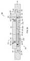
- Figure 3Ashows a partial cross sectional view of an illustrative support assembly 300.
- the support assembly 300can be at least partially disposed within the chamber body 112.
- the support assembly 300can include a support member 310 to support a substrate (not shown in this view) for processing within the chamber body 112.
- the support member 310can be coupled to a lift mechanism 330 through a shaft 314 which extends through a centrally-located opening 114 formed in a bottom surface of the chamber body 112.
- the lift mechanism 330can be flexibly sealed to the chamber body 112 by a bellows 333 that prevents vacuum leakage from around the shaft 314.
- the lift mechanism 330allows the support member 310 to be moved vertically within the chamber body 112 between a process position and a lower, transfer position.
- the transfer positionis slightly below the opening of the slit valve 160 formed in a sidewall of the chamber body 112.
- Figure 3Bshows an enlarged partial cross sectional of the support assembly 300 shown in Figure 3A.
- the support member 310has a flat, circular surface or a substantially flat, circular surface for supporting a substrate to be processed thereon.
- the support member 310is preferably constructed of aluminum.
- the support member 310can include a removable top plate 311 made of some other material, such as silicon or ceramic material, for example, to reduce backside contamination of the substrate.
- the support member 310 or the top plate 311can include a plurality of extensions or dimples 311A arranged on the upper surface thereof.
- the dimples 311Aare shown on the upper surface of the top plate 311. It can be envisioned that the dimples 311A can be arranged on the upper surface of the support member 310 if a top plate 311 is not desired.
- the dimples 311Aprovide minimum contact between the lower surface of the substrate and the support surface of the support assembly 300 (i.e. either the support member 310 or the top plate 311).
- the substratemay be secured to the support assembly 300 using a vacuum chuck.
- the top plate 311can include a plurality of holes 312 in fluid communication with one or more grooves 316 formed in the support member 310.
- the grooves 316are in fluid communication with a vacuum pump (not shown) via a vacuum conduit 313 disposed within the shaft 314 and the support member 310.
- the vacuum conduit 313can be used to supply a purge gas to the surface of the support member 310 to prevent deposition when a substrate is not disposed on the support member 310.
- the vacuum conduit 313can also pass a purge gas during processing to prevent a reactive gas or byproduct from contacting the backside of the substrate.
- the substratemay be secured to the support member 310 using an electrostatic chuck.
- the substratecan be held in place on the support member 310 by a mechanical clamp (not shown), such as a conventional clamp ring.
- an electrostatic chucktypically includes at least a dielectric material that surrounds an electrode (not shown), which may be located on an upper surface of the support member 310 or formed as an integral part of the support member 310.
- the dielectric portion of the chuckelectrically insulates the chuck electrode from the substrate and from the remainder of the support assembly 300.
- the perimeter of the chuck dielectriccan be is slightly smaller than the perimeter of the substrate.
- the substrateslightly overhangs the perimeter of the chuck dielectric so that the chuck dielectric will remain completely covered by the substrate even if the substrate is misaligned off center when positioned on the chuck. Assuring that the substrate completely covers the chuck dielectric ensures that the substrate shields the chuck from exposure to potentially corrosive or damaging substances within the chamber body 112.
- the voltage for operating the electrostatic chuckcan be supplied by a separate "chuck" power supply (not shown).
- One output terminal of the chucking power supplyis connected to the chuck electrode.
- the other output terminaltypically is connected to electrical ground, but alternatively may be connected to a metal body portion of the support assembly 300.
- the substrateis placed in contact with the dielectric portion, and a direct current voltage is placed on the electrode to create the electrostatic attractive force or bias to adhere the substrate on the upper surface of the support member 310.
- the support member 310can include one or more bores 323 formed therethrough to accommodate a lift pin 325.
- Each lift pin 325is typically constructed of ceramic or ceramic-containing materials, and are used for substrate-handling and transport.
- Each lift pin 325is slideably mounted within the bore 323.
- the bore 323is lined with a ceramic sleeve to help freely slide the lift pin 325.
- the lift pin 325is moveable within its respective bore 323 by engaging an annular lift ring 320 disposed within the chamber body 112.
- the lift ring 320is movable such that the upper surface of the lift-pin 325 can be located above the substrate support surface of the support member 310 when the lift ring 320 is in an upper position.
- each lift-pin 325passes through its respective bore 323 in the support member 310 when the lift ring 320 moves from either the lower position to the upper position.
- the lift pins 325When activated, the lift pins 325 push against a lower surface of the substrate, lifting the substrate off the support member 310. Conversely, the lift pins 325 may be de-activated to lower the substrate, thereby resting the substrate on the support member 310.
- the lift pins 325can include enlarged upper ends or conical heads to prevent the pins 325 from falling out from the support member 310. Other pin designs can also be utilized and are well known to those skilled in the art.
- one or more of the lift pins 325include a coating or an attachment disposed thereon that is made of a non-skid or highly frictional material to prevent the substrate from sliding when supported thereon.
- a preferred materialis a high temperature, polymeric material that does not scratch or otherwise damage the backside of the substrate which would create contaminants within the processing chamber 100.
- the coating or attachmentis KALREZTM coating available from DuPont.
- an actuatorsuch as a conventional pneumatic cylinder or a stepper motor (not shown).
- the stepper motor or cylinderdrives the lift ring 320 in the up or down positions, which in turn drives the lift-pins 325 that raise or lower the substrate.
- a substrate(not shown) is supported on the support member 310 by three lift-pins 325 (not shown in this view) dispersed approximately 120 degrees apart and projecting from the lift ring 320.
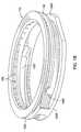
- the support assembly 300can include an edge ring 305 disposed about the support member 310.
- the edge ring 305can be made of a variety of materials such as ceramic, quartz, aluminum and steel, among others.
- the edge ring 305is an annular member that is adapted to cover an outer perimeter of the support member 310 and protect the support member 310 from deposition.
- the edge ring 305can be positioned on or adjacent the support member 310 to form an annular purge gas channel 334 between the outer diameter of support member 310 and the inner diameter of the edge ring 305.
- the annular purge gas channel 334can be in fluid communication with a purge gas conduit 335 formed through the support member 310 and the shaft 314.
- the purge gas conduit 335is in fluid communication with a purge gas supply (not shown) to provide a purge gas to the purge gas channel 334.
- a purge gas supply(not shown) to provide a purge gas to the purge gas channel 334.
- Any suitable purge gassuch as nitrogen, argon, or helium, may be used alone or in combination.
- the purge gasflows through the conduit 335, into the purge gas channel 334, and about an edge of the substrate disposed on the support member 310. Accordingly, the purge gas working in cooperation with the edge ring 305 prevents deposition at the edge and/or backside of the substrate.
- the temperature of the support assembly 300is controlled by a fluid circulated through a fluid channel 360 embedded in the body of the support member 310.
- the fluid channel 360is in fluid communication with a heat transfer conduit 361 disposed through the shaft 314 of the support assembly 300.
- the fluid channel 360is positioned about the support member 310 to provide a uniform heat transfer to the substrate receiving surface of the support member 310.
- the fluid channel 360 and heat transfer conduit 361can flow heat transfer fluids to either heat or cool the support member 310. Any suitable heat transfer fluid may be used, such as water, nitrogen, ethylene glycol, or mixtures thereof.
- the support assembly 300can further include an embedded thermocouple (not shown) for monitoring the temperature of the support surface of the support member 310.
- a signal from the thermocouplemay be used in a feedback loop to control the temperature or flowrate of the fluid circulated through the fluid channel 360.
- the support member 310can be moved vertically within the chamber body 112 so that a distance between support member 310 and the lid assembly 200 can be controlled.
- a sensor(not shown) can provide information concerning the position of support member 310 within chamber 100.
- An example of a lifting mechanism for the support member 310is described in detail in U.S. Patent No. 5,951,776, issued September 14, 1999 to Selyutin et al., entitled “Self-Aligning Lift Mechanism", which is hereby incorporated by reference in it entirety.
- the support member 310can be elevated to a close proximity of the lid assembly 200 to control the temperature of the substrate being processed.
- the substratecan be heated via radiation emitted from the distribution plate 225 that is controlled by the heating element 270.
- the substratecan be lifted off the support member 310 to close proximity of the heated lid assembly 200 using the lift pins 325 activated by the lift ring 320.
- processing chamber 100After extended periods of use or at designated times for scheduled maintenance, certain components of the processing chamber 100 including those described above can be regularly inspected, replaced, or cleaned. These components are typically parts that are collectively known as the "process kit.” Illustrative components of the process kit can include, but are not limited to the showerhead 225, the top plate 311, the edge ring 305, the liner 133, and the lift pins 325, for example. Any one or more of these components are typically removed from the chamber 100 and cleaned or replaced at regular intervals or according to an as-needed basis.
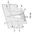
- FIG. 4Ashows a partial cross sectional view of another illustrative lid assembly 400.
- the lid assembly 400includes at least two stacked components configured to form a plasma volume or cavity therebetween.
- the lid assembly 400includes a first electrode 410 ("upper electrode”) disposed vertically above a second electrode 450 (“lower electrode”) confining a plasma volume or cavity 425 therebetween.
- the first electrode 410is connected to a power source 415, such as an RF power supply, and the second electrode 450 is connected to ground, forming a capacitance between the two electrodes 410, 450.
- a power source 415such as an RF power supply
- the lid assembly 400includes one or more gas inlets 412 (only one is shown) that are at least partially formed within an upper section 413 of the first electrode 410.
- the one or more process gasesenter the lid assembly 400 via the one or more gas inlets 412.
- the one or more gas inlets 412are in fluid communication with the plasma cavity 425 at a first end thereof and coupled to one or more upstream gas sources and/or other gas delivery components, such as gas mixers, at a second end thereof.
- the first end of the one or more gas inlets 412can open into the plasma cavity 425 at the upper most point of the inner diameter 430 of the expanding section 420 as shown in Figure 4A.
- the first end of the one or more gas inlets 412can open into the plasma cavity 425 at any height interval along the inner diameter 430 of the expanding section 420.
- two gas inlets 412can be disposed at opposite sides of the expanding section 420 to create a swirling flow pattern or "vortex" flow into the expanding section 420 which helps mix the gases within the plasma cavity 425.
- a more detailed description of such a flow pattern and gas inlet arrangementsis provided by U.S. Patent Application No. 20030079686, filed on December 21, 2001, which is incorporated by reference herein.
- the first electrode 410has an expanding section 420 that houses the plasma cavity 425. As shown in Figure 4A, the expanding section 420 is in fluid communication with the gas inlet 412 as described above. In one or more embodiments, the expanding section 420 is an annular member that has an inner surface or diameter 430 that gradually increases from an upper portion 420A thereof to a lower portion 420B thereof. As such, the distance between the first electrode 410 and the second electrode 450 is variable. That varying distance helps control the formation and stability of the plasma generated within the plasma cavity 425.
- the expanding section 420resembles a cone or "funnel," as is shown in Figures 4A and 4B.
- Figure 4Bshows an enlarged schematic, partial cross sectional view of the upper electrode of Figure 4A.
- the inner surface 430 of the expanding section 420gradually slopes from the upper portion 420A to the lower portion 420B of the expanding section 420.
- the slope or angle of the inner diameter 430can vary depending on process requirements and/or process limitations.
- the length or height of the expanding section 420can also vary depending on specific process requirements and/or limitations.
- the slope of the inner diameter 430, or the height of the expanding section 420, or bothcan vary depending on the volume of plasma needed for processing.
- the slope of the inner diameter 430can be at least 1:1, or at least 1.5:1 or at least 2:1 or at least 3:1 or at least 4:1 or at least 5:1 or at least 10:1. In one or more embodiments, the slope of the inner diameter 430 can range from a low of 2:1 to a high of 20:1.
- the expanding section 420can be curved or arced although not shown in the figures.
- the inner surface 430 of the expanding section 420can be curved or arced to be either convexed or concaved.
- the inner surface 430 of the expanding section 420can have a plurality of sections that are each sloped, tapered, convexed, or concaved.
- the expanding section 420 of the first electrode 410varies the vertical distance between the first electrode 410 and the second electrode 450 because of the gradually increasing inner surface 430 of the first electrode 410. That variable distance is directly related to the power level within the plasma cavity 425.
- the variation in distance between the two electrodes 410, 450allows the plasma to find the necessary power level to sustain itself within some portion of the plasma cavity 425 if not throughout the entire plasma cavity 425.
- the plasma within the plasma cavity 425is therefore less dependent on pressure, allowing the plasma to be generated and sustained within a wider operating window. As such, a more repeatable and reliable plasma can be formed within the lid assembly 400.
- the first electrode 410can be constructed from any process compatible materials, such as aluminum, anodized aluminum, nickel plated aluminum, nickel plated aluminum 6061-T6, stainless steel as well as combinations and alloys thereof, for example.
- the entire first electrode 410 or portions thereofare nickel coated to reduce unwanted particle formation.
- at least the inner surface 430 of the expanding section 420is nickel plated.
- the second electrode 450can include one or more stacked plates. When two or more plates are desired, the plates should be in electrical communication with one another. Each of the plates should include a plurality of apertures or gas passages to allow the one or more gases from the plasma cavity 425 to flow through.
- the lid assembly 400can further include an isolator ring 440 to electrically isolate the first electrode 410 from the second electrode 450.
- the isolator ring 440can be made from aluminum oxide or any other insulative, process compatible material.
- the isolator ring 440surrounds or substantially surrounds at least the expanding section 420 as shown in Figure 4B.
- the second electrode 450includes a top plate 460, distribution plate 470 and blocker plate 480.
- the top plate 460, distribution plate 470 and blocker plate 480are stacked and disposed on a lid rim 490 which is connected to the chamber body 112 as shown in Figure 4B.
- a hinge assembly(not shown) can be used to couple the lid rim 490 to the chamber body 112.
- the lid rim 490can include an embedded channel or passage 492 for housing a heat transfer medium.
- the heat transfer mediumcan be used for heating, cooling, or both, depending on the process requirements. Illustrative heat transfer mediums are listed above.
- the top plate 460includes a plurality of gas passages or apertures 465 formed beneath the plasma cavity 425 to allow gas from the plasma cavity 425 to flow therethrough.
- the top plate 460can include a recessed portion 462 that is adapted to house at least a portion of the first electrode 410.
- the apertures 465are through the cross section of the top plate 460 beneath the recessed portion 462.
- the recessed portion 462 of the top plate 460can be stair stepped as shown in Figure 4A to provide a better sealed fit therebetween.
- the outer diameter of the top plate 460can be designed to mount or rest on an outer diameter of the distribution plate 470 as shown in Figure 4A.
- An o-ring type sealsuch as an elastomeric o-ring 463, can be at least partially disposed within the recessed portion 462 of the top plate 460 to ensure a fluid-tight contact with the first electrode 410.
- an o-ring type seal 466can be used to provide a fluid-tight contact between the outer perimeters of the top plate 460 and the distribution plate 470.
- the distribution plate 470is identical to the distribution plate 225 shown and described above with reference to Figures 2A-2C.
- the distribution plate 470is substantially disc-shaped and includes a plurality of apertures 475 or passageways to distribute the flow of gases therethrough.
- the apertures 475can be sized and positioned about the distribution plate 470 to provide a controlled and even flow distribution to the chamber body 112 where the substrate to be processed is located.
- the apertures 475prevent the gas(es) from impinging directly on the substrate surface by slowing and re-directing the velocity profile of the flowing gases, as well as evenly distributing the flow of gas to provide an even distribution of gas across the surface of the substrate.
- the distribution plate 470can also include an annular mounting flange 472 formed at an outer perimeter thereof.
- the mounting flange 472can be sized to rest on an upper surface of the lid rim 490.
- An o-ring type sealsuch as an elastomeric o-ring, can be at least partially disposed within the annular mounting flange 472 to ensure a fluid-tight contact with the lid rim 490.
- the distribution plate 470includes one or more embedded channels or passages 474 for housing a heater or heating fluid to provide temperature control of the lid assembly 400. Similar to the lid assembly 200 described above, a resistive heating element can be inserted within the passage 474 to heat the distribution plate 470. A thermocouple can be connected to the distribution plate 470 to regulate the temperature thereof. The thermocouple can be used in a feedback loop to control electric current applied to the heating element, as described above.
- a heat transfer mediumcan be passed through the passage 474.
- the one or more passages 474can contain a cooling medium, if needed, to better control temperature of the distribution plate 470 depending on the process requirements within the chamber body 112.
- any heat transfer mediummay be used, such as nitrogen, water, ethylene glycol, or mixtures thereof, for example.
- the lid assembly 400can be heated using one or more heat lamps (not shown).
- the heat lampsare arranged about an upper surface of the distribution plate 470 to heat the components of the lid assembly 400 including the distribution plate 470 by radiation.
- the blocker plate 480is optional and would be disposed between the top plate 460 and the distribution plate 470.
- the blocker plate 480is removably mounted to a lower surface of the top plate 460.
- the blocker plate 480should make good thermal and electrical contact with the top plate 460.
- the blocker plate 480can be coupled to the top plate 460 using a bolt or similar fastener.
- the blocker plate 480can also be threaded or screwed onto an out diameter of the top plate 460.
- the blocker plate 480includes a plurality of apertures 485 to provide a plurality of gas passages from the top plate 460 to the distribution plate 470.
- the apertures 485can be sized and positioned about the blocker plate 480 to provide a controlled and even flow distribution the distribution plate 470.
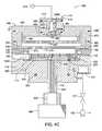
- Figure 4Cshows a partial cross sectional view of the chamber body 112 having the lid assembly 400 disposed thereon.
- the expanding section 420is centered above the support assembly 300 as shown in Figure 4C.
- the confinement of the plasma within the plasma cavity 425 and the central location of the confined plasmaallows an even and repeatable distribution of the disassociated gas(es) into the chamber body 112.
- the gas leaving the plasma volume 425flows through the apertures 465 of the top plate 460 to the upper surface of the blocker plate 480.
- the apertures 485 of the blocker plate 480distribute the gas to the backside of the distribution plate 470 where the gas is further distributed through the apertures 475 of the distribution plate 470 before contacting the substrate (not shown) within the chamber body 112.
- NH3ammonia
- NF3nitrogen trifluoride
- the dry etch processbegins by placing a substrate (not shown), such as a semiconductor substrate for example, into the processing chamber 100.
- the substrateis typically placed into the chamber body 112 through the slit valve opening 160 and disposed on the upper surface of the support member 310.
- the substrateis chucked to the upper surface of the support member 310, and an edge purge is passed through the channel 334.
- the substrateis chucked to the upper surface of the support member 310 by pulling a vacuum through the holes 312 and grooves 316 that are in fluid communication with a vacuum pump via conduit 313.
- the support member 310is then lifted to a processing position within the chamber body 112, if not already in a processing position.
- the chamber body 112is preferably maintained at a temperature of between 50°C and 80°C, more preferably at about 65°C. This temperature of the chamber body 112 is maintained by passing a heat transfer medium through the fluid channel 113.
- the substrateis cooled below 65°C, such as between 15°C and 50°C, by passing a heat transfer medium or coolant through the fluid channel 360 formed within the support assembly 300.
- the substrateis maintained below room temperature.
- the substrateis maintained at a temperature of between 22°C and 40°C.
- the support member 310is maintained below about 22°C to reach the desired substrate temperatures specified above.
- the coolantis passed through the fluid channel 360.
- a continuous flow of coolantis preferred to better control the temperature of the support member 310.
- the coolantis preferably 50 percent by volume ethylene glycol and 50 percent by volume water. Of course, any ratio of water and ethylene glycol can be used so long as the desired temperature of the substrate is maintained.
- the ammonia and nitrogen trifluoride gasesare then introduced into the chamber 100 to form a cleaning gas mixture.
- the amount of each gas introduced into the chamberis variable and may be adjusted to accommodate, for example, the thickness of the oxide layer to be removed, the geometry of the substrate being cleaned, the volume capacity of the plasma, the volume capacity of the chamber body 112, as well as the capabilities of the vacuum system coupled to the chamber body 112.
- the gasesare added to provide a gas mixture having at least a 1:1 molar ratio of ammonia to nitrogen trifluoride.
- the molar ratio of the gas mixtureis at least about 3 to 1 (ammonia to nitrogen trifluoride).
- the gasesare introduced in the chamber 100 at a molar ratio of from 5:1 (ammonia to nitrogen trifluoride) to 30:1. More preferably, the molar ratio of the gas mixture is of from about 5 to 1 (ammonia to nitrogen trifluoride) to about 10 to 1. The molar ratio of the gas mixture may also fall between about 10:1 (ammonia to nitrogen trifluoride) and about 20:1.
- a purge gas or carrier gasmay also be added to the gas mixture.
- Any suitable purge/carrier gasmay be used, such as argon, helium, hydrogen, nitrogen, or mixtures thereof, for example.
- the overall gas mixtureis from about 0.05% to about 20% by volume of ammonia and nitrogen trifluoride. The remainder being the carrier gas.
- the purge or carrier gasis first introduced into the chamber body 112 before the reactive gases to stabilize the pressure within the chamber body 112.
- the operating pressure within the chamber body 112can be variable. Typically, the pressure is maintained between about 500 mTorr and about 30 Torr. Preferably, the pressure is maintained between about 1 Torr and about 10 Torr. More preferably, the operating pressure within the chamber body 112 is maintained between about 3 Torr and about 6 Torr.
- An RF power of from about 5 and about 600 Wattsis applied to the electrode 240 to ignite a plasma of the gas mixture within the volumes 261, 262, and 263 contained in the gas delivery assembly 220.
- the RF poweris less than 100 Watts. More preferable is that the frequency at which the power is applied is very low, such as less than 100 kHz. Preferably, the frequency ranges from about 50 kHz to about 90 kHz.
- the plasma energydissociates the ammonia and nitrogen trifluoride gases into reactive species that combine to form a highly reactive ammonia fluoride (NH4F) compound and/or ammonium hydrogen fluoride (NH4F ⁇ HF) in the gas phase. These molecules then flow through the gas delivery assembly 220 via the holes 225A of the distribution plate 225 to react with the substrate surface to be cleaned.
- the carrier gasis first introduced into the chamber 100, a plasma of the carrier gas is generated, and then the reactive gases, ammonia and nitrogen trifluoride, are added to the plasma.
- the etchant gasNH4F and/or NH4F ⁇ HF, reacts with the silicon oxide surface to form ammonium hexafluorosilicate (NH4)2SiF6, NH3, and H2O products.
- the NH3, and H2Oare vapors at processing conditions and removed from the chamber 100 by the vacuum pump 125.
- the volatile gasesflow through the apertures 135 formed in the liner 133 into the pumping channel 129 before the gases exit the chamber 100 through the vacuum port 131 into the vacuum pump 125.
- a thin film of (NH4)2SiF6is left behind on the substrate surface.
- the support member 310 having the substrate supported thereonis elevated to an anneal position in close proximity to the heated distribution plate 225.
- the heat radiated from the distribution plate 225should be sufficient to dissociate or sublimate the thin film of (NH4)2SiF6 into volatile SiF4, NH3, and HF products.
- These volatile productsare then removed from the chamber 100 by the vacuum pump 125 as described above.
- a temperature of 75°C or moreis used to effectively sublimate and remove the thin film from the substrate.
- a temperature of 100°C or moreis used, such as between about 115°C and about 200°C.
- the thermal energy to dissociate the thin film of (NH4)2SiF6 into its volatile componentsis convected or radiated by the distribution plate 225.
- a heating element 270is directly coupled to the distribution plate 225, and is activated to heat the distribution plate 225 and the components in thermal contact therewith to a temperature between about 75°C and 250°C.
- the distribution plate 225is heated to a temperature of between 100°C and 150°C, such as about 120°C.
- the lift mechanism 330can elevate the support member 310 toward a lower surface of the distribution plate 225.
- the substrateis secured to the support member 310, such as by the vacuum chuck or electrostatic chuck described above.
- the substratecan be lifted off the support member 310 and placed in close proximity to the heated distribution plate 225 by elevating the lift pins 325 via the lift ring 320.
- the distance between the upper surface of the substrate having the thin film thereon and the distribution plate 225is not critical and is a matter of routine experimentation. A person of ordinary skill in the art can easily determine the spacing required to efficiently and effectively vaporize the thin film without damaging the underlying substrate. It is believed, however, that a spacing of between about 0.254 mm (10 mils) and 5.08 mm (200 mils) is effective.
- the chamberis purged and evacuated.
- the cleaned substrateis then removed from the chamber body 112 by lowering the substrate to the transfer position, de-chucking the substrate, and transferring the substrate through the slit valve opening160.
- a system controller(not shown) can be used to regulate the operations of the processing chamber 100.
- the system controllercan operate under the control of a computer program stored on a hard disk drive of a computer.
- the computer programcan dictate the process sequencing and timing, mixture of gases, chamber pressures, RF power levels, susceptor positioning, slit valve opening and closing, wafer cooling and other parameters of a particular process.
- the interface between a user and the system controllercan be made via a CRT monitor and light pen (not shown).
- two monitorsare used, one monitor mounted in the clean room wall for the operators and the other monitor behind the wall for the service technicians. Also preferred is that both monitors simultaneously display the same information but only one light pen is enabled.
- the light pendetects light emitted by the CRT display with a light sensor in the tip of the pen. To select a particular screen or function, the operator can touch a designated area of the display screen and push the button on the pen.
- the display screengenerally confirms communication between the light pen and the touched area by changing its appearance, i.e. highlight or color, or displaying a new menu or screen.
- a variety of processescan be implemented using a computer program product that runs on, for example, the system controller.
- the computer program codecan be written in any conventional computer readable programming language such as for example 68000 assembly language, C, C++, or Pascal.
- Suitable program codecan be entered into a single file, or multiple files, using a conventional text editor, and stored or embodied in a computer usable medium, such as a memory system of the computer. If the entered code text is in a high level language, the code is compiled, and the resultant compiler code is then linked with an object code of precompiled library routines. To execute the linked compiled object code, the system user invokes the object code, causing the computer system to load the code in memory, from which the CPU reads and executes the code to perform the tasks identified in the program.
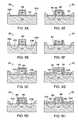
- Figures 5A-5Hare sectional schematic views of an exemplary fabrication sequence for forming an exemplary active electronic device, such as a MOSFET structure 500, utilizing the dry etch process and the processing chamber 100 described herein.
- the exemplary MOSFET structuremay be formed on a semiconductor material, for example a silicon or gallium arsenide substrate 525.
- the substrate 525is a silicon wafer having a ⁇ 100> crystallographic orientation and a diameter of 150 mm (6 inches), 200 mm (8 inches), or 300 mm (12 inches).
- the MOSFET structureincludes a combination of (i) dielectric layers, such as silicon dioxide, organosilicate, carbon doped silicon oxide, phosphosilicate glass (PSG), borophosphosilicate glass (BPSG), silicon nitride, or combinations thereof; (ii) semiconducting layers such as doped polysilicon, and n-type or p-type doped monocrystalline silicon; and (iii) electrical contacts and interconnect lines formed from layers of metal or metal silicide, such as tungsten, tungsten silicide, titanium, titanium silicide, cobalt silicide, nickel silicide, or combinations thereof.
- dielectric layerssuch as silicon dioxide, organosilicate, carbon doped silicon oxide, phosphosilicate glass (PSG), borophosphosilicate glass (BPSG), silicon nitride, or combinations thereof
- semiconducting layerssuch as doped polysilicon, and n-type or p-type doped monocrystalline silicon
- fabrication of the active electronic devicebegins by forming electrical isolation structures that electrically isolate the active electronic device from other devices.
- electrical isolation structuresThere are several types of electrical isolation structures as generally described in VLSI Technology, Second Edition, Chapter 11, by S. M. Sze, McGraw-Hill Publishing Company (1988), which is incorporated herein by reference.
- a field oxide layer(not shown) having a thickness of about 2,000 angstroms is first grown over the entire substrate 525, and portions of the oxide layer are removed to form the field oxide barriers 545A,B which surround exposed regions in which the electrically active elements of the device are formed.
- the exposed regionsare thermally oxidized to form a thin gate oxide layer 550 having a thickness of from about 50 to 300 angstroms.
- a polysilicon layeris then deposited, patterned, and etched to create a gate electrode 555.
- the surface of the polysilicon gate electrode 555can be reoxidized to form an insulating dielectric layer 560, providing the structure shown in Figure 5A.
- the source and drain 570A,Bare next formed by doping the appropriate regions with suitable dopant atoms.
- an n-type dopant speciescomprising arsenic or phosphorous is used.
- the dopingis performed by an ion implanter and might include, for example, phosphorous (31P) at a concentration of about 1013 atoms/cm2 at an energy level of from about 30 to 80 Kev, or Arsenic (75As) at a dose of from about 1015 to 1017 atoms/cm2 and an energy of from 10 to 100 Kev.
- the dopantis driven into the substrate 525 by heating the substrate, for example, in a rapid thermal processing (RTP) apparatus.
- RTPrapid thermal processing
- the oxide layer 550 covering the source and drain regions 570A,Bis stripped in a conventional stripping process to remove any impurities caused by the implantation process which are trapped in the oxide layer, providing the structure shown in Figure 8B.
- a silicon nitride layer 575is deposited on the gate electrode 555 and the surfaces on the substrate 525 by low-pressure chemical vapor deposition (LPCVD) using a gas mixture of SiH2, Cl2, and NH3.
- LPCVDlow-pressure chemical vapor deposition
- the silicon nitride layer 575is then etched using reactive ion etching (RIE) techniques to form nitride spacers 580 on the sidewall of the gate electrode 555, as shown in Figure 5D.
- RIEreactive ion etching
- the electrical isolation sidewall spacers 580 and overlayerscan be fabricated from other materials, such as silicon oxide.
- the silicon oxide layers used to form sidewall spacers 580are typically deposited by CVD or PECVD from a feed gas of tetraethoxysilane (TEOS) at a temperature in the range of from about 600°C to about 1,000°C.
- TEOStetraethoxysilane
- a native silicon oxide layer 585is formed on exposed silicon surfaces by exposure to the atmosphere before and after the processes.
- the native silicon oxide layer 585must be removed prior to forming conductive metal silicide contacts on the gate 555, source 570A, and drain 570B to improve the alloying reaction and electrical conductivity of the metal suicide formed.
- the native silicon oxide layer 585can increase the electrical resistance of the semiconducting material, and adversely affect the silicidation reaction of the silicon and metal layers that are subsequently deposited. Therefore, it is necessary to remove this native silicon dioxide layer 585 using the dry etch process described prior to forming metal silicide contacts or conductors for interconnecting active electronic devices.
- the dry etch processremoves the native silicon oxide layers 585 to expose the source 570A, drain 570B, and the top surface of the gate electrode 555 as shown in Figure 5F.
- a PVD sputtering processis used to deposit a layer of metal 590.
- Conventional furnace annealingis then used to anneal the metal and silicon layers to form metal silicide in regions in which the metal layer 590 is in contact with silicon.
- the annealis typically performed in a separate processing system.
- a protective cap layer(not shown) may be deposited over the metal 590.
- the cap layersare typically nitride materials and may include one or more materials selected from the group consiting of titanium nitride, tungsten nitride, tantalum nitride, nafnium nitride, and silicon nitride.
- the cap layermay be deposited by any deposition process, preferably by PVD.
- Annealingtypically involves heating the substrate 500 to a temperature of between 600°C and 800°C in an atmosphere of nitrogen for about 30 minutes.
- the metal silicide 595can be formed utilizing a rapid thermal annealing process in which the substrate 500 is rapidly heated to about 1000°C for about 30 seconds.
- Suitable conductive metalsinclude cobalt, titanium, nickel, tungsten, platinum, and any other metal that has a low contact resistance and that can form a reliable metal silicide contact on both polysilicon and monocrystalline silicon.
- Unreacted portions of the metal layer 590can be removed by a wet etch using aqua regia, (HCl and HNO3) which removes the metal without attacking the metal silicide 595; the spacer 580, or the field oxide 545A,B, thus leaving a self-aligned metal silicide contact 595 on the gate 555, source 570A, and drain 570B, as shown in Figure 5H.
- an insulating cover layercomprising, for example, silicon oxide, BPSG, or PSG, can be deposited on the electrode structures.
- the insulating cover layeris deposited by means of chemical-vapor deposition in a CVD chamber, in which the material condenses from a feed gas at low or atmospheric pressure, as for example, described in commonly assigned U.S. Pat. No. 5,500,249, issued March 19, 1996, which is incorporated herein by reference. Thereafter, the structure 500 is annealed at glass transition temperatures to form a smooth planarized surface.
- the processing chamber 100can be integrated into a multi-processing platform, such as an Endura ⁇ platform available from Applied Materials, Inc. located in Santa Clara, California. Such a processing platform is capable of performing several processing operations without breaking vacuum. Details of the Endura ⁇ platform are described in commonly assigned U.S. Patent Application Serial No. 09/451,628, entitled “Integrated Modular Processing Platform", filed on November 30, 1999, which is incorporated by reference herein.
- FIG. 6is a schematic top-view diagram of an illustrative multi-chamber processing system 600.
- the system 600can include one or more load lock chambers 602, 604 for transfering of substrates into and out of the system 600.
- the load lock chambers 602, 604may "pump down" the substrates introduced into the system 600.
- a first robot 610may transfer the substrates between the load lock chambers 602, 604, and a first set of one or more substrate processing chambers 612, 614, 616, 618 (four are shown).
- Each processing chamber 612, 614, 616, 618can be outfitted to perform a number of substrate processing operations including the dry etch processes described herein in addition to cyclical layer deposition (CLD), atomic layer deposition (ALD), chemical vapor deposition (CVD), physical vapor deposition (PVD), etch, pre-clean, degas, orientation and other substrate processes.
- CLDcyclical layer deposition
- ALDatomic layer deposition
- CVDchemical vapor deposition
- PVDphysical vapor deposition
- etchpre-clean, degas, orientation and other substrate processes.
- the first robot 610can also transfer substrates to/from one or more transfer chambers 622, 624.
- the transfer chambers 622, 624can be used to maintain ultrahigh vacuum conditions while allowing substrates to be transferred within the system 600.
- a second robot 630can transfer the substrates between the transfer chambers 622, 624 and a second set of one or more processing chambers 632, 634, 636, 638.
- the processing chambers 632, 634, 636, 638can be outfitted to perform a variety of substrate processing operations including the dry etch processes described herein in addition to cyclical layer deposition (CLD), atomic layer deposition (ALD), chemical vapor deposition (CVD), physical vapor deposition (PVD), etch, pre-clean, degas, and orientation, for example.
- CLDcyclical layer deposition
- ALDatomic layer deposition
- CVDchemical vapor deposition
- PVDphysical vapor deposition
- etchpre-clean
- degasdegas
- orientationorientation
- An illustrative multi-processing system 600 for forming the MOSFET structure of Figures 5A-5Hcan include two ptocessing chambers 100 as described above, two physical vapor deposition chambers to deposit the metal 500 and two physical vapor deposition chambers to deposit the optional cap layer (not shown). Any one of the processing chambers 612, 614, 616, 618, 632, 634, 636, 638 shown in Figure 6 represent the PVD chambers and/or processing chambers 100.
- the dry etch process described hereincan also be used to form other semiconductor structures and devices that have other metal silicide layers, for example, suicides of tungsten, tantalum, molybdenum.
- the cleaning processcan also be used prior to the deposition of layers of different metals including, for example, aluminum, copper, cobalt, nickel, silicon, titanium, palladium, hafnium, boron, tungsten, tantalum, or mixtures thereof.
- etcha gas mixture of 2 sccm of NF3, 10 sccm of NH3 and 2,500 sccm of argon was introduced into the chamber.
- a plasma of the gas mixturewas ignited using 100 Watts of power.
- the bottom purgewas 1,500 sccm of argon and the edge purge was 50 sccm of argon.
- the chamber pressurewas maintained at about 6 Torr, and the substrate temperature was about 22°C.
- the substratewas etched for 120 seconds.
- the spacingwas 750 mil and the lid temperature was 120°C.
- the substratewas annealed for about 60 seconds. About 50 angstroms of material was removed from the substrate surface. No anneal effect was observed. The etch rate was about 0.46 angstroms per second (28 ⁇ /min). The observed etch uniformity was about 5 % for the 50 ⁇ etch.
Landscapes
- Engineering & Computer Science (AREA)
- Chemical & Material Sciences (AREA)
- Physics & Mathematics (AREA)
- Plasma & Fusion (AREA)
- Analytical Chemistry (AREA)
- Condensed Matter Physics & Semiconductors (AREA)
- Power Engineering (AREA)
- Microelectronics & Electronic Packaging (AREA)
- Computer Hardware Design (AREA)
- Manufacturing & Machinery (AREA)
- General Physics & Mathematics (AREA)
- Chemical Kinetics & Catalysis (AREA)
- Organic Chemistry (AREA)
- Metallurgy (AREA)
- Mechanical Engineering (AREA)
- Materials Engineering (AREA)
- Public Health (AREA)
- Epidemiology (AREA)
- Health & Medical Sciences (AREA)
- General Chemical & Material Sciences (AREA)
- Inorganic Chemistry (AREA)
- Drying Of Semiconductors (AREA)
- Chemical Vapour Deposition (AREA)
- Electrodes Of Semiconductors (AREA)
- Internal Circuitry In Semiconductor Integrated Circuit Devices (AREA)
- Cleaning Or Drying Semiconductors (AREA)
Abstract

Description
Claims (80)
- A processing chamber for removing native oxides from asubstrate surface, comprising:a chamber body;a support assembly at least partially disposed withinthe chamber body and adapted to support a substrate thereon,wherein the support assembly includes one or more fluidchannels at least partially formed therein and capable ofcooling the substrate; anda lid assembly disposed on an upper surface of thechamber body, the lid assembly comprising a first electrodeand a second electrode that define a plasma cavitytherebetween, wherein the second electrode is heated andadapted to convectively heat the substrate.
- A chamber as claimed in claim 1, wherein the supportassembly is adapted to move vertically within the chamberbody to locate the substrate in a heating position proximatethe second electrode and to locate the substrate in an etchposition removed from the second electrode.
- A chamber as claimed claim 1 or claim 2, wherein thesupport assembly comprises a receiving surface adapted tosupport the substrate thereon, wherein the receiving surfaceis disposed above a shaft coupled to a lift mechanism.
- A chamber as claimed in claim 3, wherein the liftmechanism is adapted to move the receiving surfacevertically within the chamber body to locate the substratein a heating position proximate the second electrode and to locate the substrate in an etch position removed from thesecond electrode.
- A chamber as claimed in claim 3 or claim 4, wherein thesupport assembly comprises one or more gas passageways thatare in fluid communication with the receiving surface at oneend thereof, and a purge gas source or vacuum source at asecond end thereof.
- A chamber as claimed in claim 5, wherein the shaftcomprises one or more embedded gas conduits adapted todeliver one or more fluids to the gas passageways.
- A chamber as claimed in any of claims 3 to 6, whereinthe receiving surface comprises one or more recessedchannels formed on an upper surface thereof.
- A chamber as claimed in claim 7, wherein the one ormore recessed channels are substantially concentric.
- A chamber as claimed in any of claims claim 1 to 8,wherein the one or more fluid channels are disposed withinthe support assembly below the receiving surface.
- A chamber as claimed in claim 9, wherein the shaftcomprises one or more embedded conduits that are in fluidcommunication with the fluid channels.
- A chamber as claimed in claim 10, wherein the one ormore embedded conduits are adapted to deliver a heatingmedium to the one or more fluid channels.
- A chamber as claimed in claim 10, wherein the one ormore embedded conduits are adapted to deliver a coolant tothe one or more fluid channels.
- A chamber as claimed in any of the preceding claims,wherein the second electrode comprises a blocker assemblycoupled to a showerhead.
- A chamber as claimed in claim 13, wherein the blockerassembly and the showerhead each comprise a plurality ofapertures formed therethrough that cooperate to evenlydistribute a gas into the chamber body.
- A chamber as claimed in any of the preceding claims,wherein the second electrode comprises a heating elementcoupled to a power source for controlling the temperature ofthe second electrode.
- A chamber as claimed in any of the preceding claims,wherein the plasma cavity is adapted to contain a plasma ofreactive gases within the lid assembly.
- A chamber as claimed in any of the preceding claims,wherein the first electrode is coupled to a radio frequencysource, microwave source, or a source of direct current, andthe second electrode is grounded.
- A method for etching native oxides from a substratesurface, comprising:loading a substrate to be processed within a processingchamber, the chamber comprising:a chamber body;a support assembly at least partially disposed withinthe chamber body and adapted to support a substrate thereon,wherein the support assembly includes one or more fluidchannels at least partially formed therein that are capableof cooling the substrate; anda lid assembly disposed on an upper surface of thechamber body, the lid assembly comprising a first electrodeand a second electrode which define a plasma cavitytherebetween, wherein the second electrode is adapted toconnectively heat the substrate;generating a plasma of reactive gas within the plasmacavity;cooling the substrate by flowing a heat transfer mediumthrough the one or more fluid channels of the supportassembly;flowing the reactive gas through the second electrodeto the substrate surface;etching the substrate surface with the reactive gas;heating the second electrode by applying power to aheating element in contact therewith; andheating the substrate using the heated second electrodeby placing the support assembly in close proximity to theheated second electrode.
- A method as claimed in claim 18, wherein cooling thesubstrate comprises maintaining a substrate temperaturebelow room temperature.
- A method as claimed in claim 18 or claim 19, whereinheating the substrate comprises maintaining the substratetemperature above 75°C.
- A lid assembly for semiconductor processing,comprising:a first electrode comprising an expanding section thathas a gradually increasing inner diameter; anda second electrode disposed opposite the first electrode,wherein a plasma cavity is defined between the innerdiameter of the expanding section of the first electrode anda first surface of the second electrode.
- A lid assembly as claimed in claim 21, wherein thesecond electrode includes a heating element coupled to asource of thermal energy to heat the second electrode.
- A lid assembly as claimed in claim 21, furthercomprising an isolation ring disposed about an outerdiameter of the expanding section.
- A lid assembly as claimed in claim 23, wherein theisolation ring and the expanding section of the firstelectrode fit within a recess formed in the first surface ofthe second electrode.
- A lid assembly as claimed in claim 21, wherein thesecond electrode comprises a plurality of gas passages thatare in fluid communication with the plasma cavity.
- A lid assembly as claimed in claim 25, wherein thesecond electrode includes a notched outer diameter formounting on a chamber body.
- A lid assembly as claimed in claim 25, furthercomprising a first perforated plate disposed opposite a second surface of the second electrode, wherein theperforations of the first perforated plate are in fluidcommunication with the plurality of gas passages of thesecond electrode.
- A lid assembly as claimed in claim 27, furthercomprising a second perforated plate disposed between thefirst perforated plate and the second electrode, wherein theperforations of the second perforated plate are in fluidcommunication with the perforations of the first perforatedplate and the plurality of gas passages of the secondelectrode.
- A lid assembly as claimed in claim 28, wherein thesecond electrode and the first perforated plate eachcomprise a notched outer diameter, and wherein the notchedouter diameter of the second electrode is adapted to mounton the notched outer diameter of the first perforated plate.
- A lid assembly as claimed in claim 29, wherein thenotched outer diameter of the first perforated plate isadapted to mount on a chamber body.
- A lid assembly for semiconductor processing,comprising:a first electrode comprising an expanding sectionhaving a gradually increasing inner diameter;a second electrode disposed opposite the firstelectrode, wherein the second electrode comprises aplurality of gas passages formed therethrough and wherein aplasma cavity is defined between the inner diameter of the expanding section of the first electrode and a first surfaceof the second electrode; anda perforated plate disposed opposite a second surfaceof the second electrode, wherein:the perforations of the perforated plate are in fluidcommunication with the plurality of gas passages of thesecond electrode;the second electrode and the perforated plate eachcomprise a notched outer diameter; andthe notched outer diameter of the second electrode isadapted to mount on the notched outer diameter of theperforated plate.
- A lid assembly as claimed in claim 31, wherein theperforated plate includes a fluid channel embedded in anouter diameter thereof for conveying a heating medium toheat the perforated plate.
- A lid assembly as claimed in claim 31, wherein theperforated plate convectively heats the second electrode.
- A lid assembly as claimed in claim 31, furthercomprising an isolation ring disposed about an outerdiameter of the expanding section.
- A lid assembly as claimed in claim 34, wherein theisolation ring and the expanding section of the firstelectrode fit within a recess formed in the first surface ofthe second electrode.
- A lid assembly for semiconductor processing,comprising:a first electrode comprising an expanding sectionhaving a gradually increasing inner diameter;a second electrode disposed opposite the firstelectrode, wherein the second electrode comprises aplurality of gas passages formed therethrough and wherein aplasma cavity is defined between the inner diameter of theexpanding section of the first electrode and a first surfaceof the second electrode;a first perforated plate disposed opposite a secondsurface of the second electrode; anda second perforated plate disposed between the secondelectrode and the first perforated plate, wherein:the second electrode and the first perforated plateeach comprise a notched outer diameter;the notched outer diameter of the second electrode isadapted to mount on the notched outer diameter of the firstperforated plate; andat least a portion of the second perforated plate isadapted to mount to the second surface of the secondelectrode.
- A lid assembly as claimed in claim 36, wherein thefirst perforated plate includes a fluid channel embedded inan outer diameter thereof for conveying a heating medium toheat the first perforated plate.
- A lid assembly as claimed in claim 36, furthercomprising an isolation ring disposed about an outerdiameter of the expanding section, wherein the isolationring and the expanding section of the first electrode fitwithin a recess formed in the first surface of the secondelectrode.
- A lid assembly as claimed in claim 36, wherein theexpanding section of the first electrode is connected to aRF power source and adapted to confine a plasma of reactivegases within the plasma cavity.
- A lid assembly as claimed in claim 36, wherein theperforations of the first and second perforated plates arein fluid communication with the gas passages of the secondelectrode.
- A method for removing native oxides from a substratesurface, comprising:supporting the substrate surface in a vacuum chamber;generating reactive species from a gas mixture withinthe chamber;cooling the substrate surface within the chamber;directing the reactive species to the cooled substratesurface to react with the native oxides thereon and form afilm on the substrate surface; andheating the substrate surface within the chamber tovaporize the film.
- A method as claimed in claim 41, further comprisingremoving the vaporized film from the chamber.
- A method as claimed in claim 41, wherein the film is asalt comprising nitrogen and fluorine atoms.
- A method as claimed in claim 41, wherein the gasmixture comprises ammonia and nitrogen fluoride.
- A method as claimed in claim 41, wherein cooling thesubstrate surface comprises flowing a coolant through asupport assembly having the substrate surface disposedthereon and maintaining the substrate temperature below roomtemperature.
- A method as claimed in claim 45, wherein the substratetemperature is maintained below about 22°C.
- A method as claimed in claim 41, wherein heating thesubstrate surface comprises positioning the substratesurface adjacent a heated gas distribution plate disposedwithin the vacuum chamber and maintaining the substratetemperature above about 100°C.
- A method as claimed in claim 47, wherein the substratetemperature is maintained at about 120°C.
- A method as claimed in claim 47, wherein the substratesurface is located between about 10 mils and 200 mils fromthe heated gas distribution plate.
- A method as claimed in claim 41, wherein directing thereactive species to the cooled substrate surface comprisesflowing the reactive species through a gas distributionplate.
- A method as claimed in claim 50, wherein heating thesubstrate surface comprises heating the gas distributionplate and positioning the substrate surface in closeproximity to the gas distribution plate.
- A method as claimed in claim 51, wherein the substratesurface is heated above about 100°C.
- A method as claimed in claim 52, wherein heating thegas distribution plate comprises coupling a heating elementto at least a portion of the gas distribution plate.
- A method as claimed in claim 53, wherein the gasdistribution plate is maintained at a temperature betweenabout 100°C and about 150°C while heating the substratesurface within the chamber to sublimate the film.
- A method as claimed in claim 44, wherein the gasmixture further comprises a carrier gas.
- A method as claimed in claim 44, wherein the gasmixture comprises at least a 3 to 1 molar ratio of ammoniato nitrogen trifluoride.
- A method as claimed in claim 56, wherein the molarratio of ammonia to nitrogen trifluoride is between about10:1 and about 20:1.
- A method as claimed in claim 51, wherein the substratesurface is located between about 10 mils and 200 mils fromthe heated gas distribution plate.
- A method for removing native oxides from a substratesurface within a single vacuum chamber, comprising:generating a plasma of reactive species in a firstsection of the chamber;cooling the substrate surface having the native oxidesthereon in a second section of the chamber;flowing the reactive species from the first section tothe second section to react with the cooled substratesurface;depositing a film on the cooled substrate surface;moving the substrate surface to a third section of thechamber; andheating the substrate surface in the third section ofthe chamber to sublimate the film.
- A method for removing native oxides from a substratesurface within a single processing chamber, comprising:generating a plasma of reactive species comprisingnitrogen and fluorine atoms;exposing the substrate surface to the reactive species;cooling the substrate surface to a temperature belowabout 22°C;depositing a film of the nitrogen and fluorine atoms onthe chilled substrate surface; andannealing the substrate surface to sublimate the film.
- A substrate support assembly, comprising:a body having one or more fluid conduits disposedtherethrough;a support member disposed on a first end of the body,the support member having one or more fluid channels formedin an upper surface thereof, wherein each fluid channel isin communication with the one or more of the fluid conduits;a cooling medium source in fluid communication with theone or more fluid conduits; anda first electrode having a plurality of holes formedtherethrough, the first electrode disposed on the uppersurface of the support member such that each of theplurality of holes is in fluid communication with at leastone of the one or more fluid channels formed in the uppersurface of the support member.
- An apparatus as claimed in claim 61, wherein at leastone of the one or more fluid conduits is in fluidcommunication with a vacuum pump for chucking a substrate tothe first electrode.
- An apparatus as claimed in claim 61, wherein at leastone of the one or more fluid conduits provides a purge gasto the one or more fluid channels formed in the uppersurface of the support member for preventing deposition on asidewall of the support member.
- An apparatus as claimed in claim 61, wherein at leastone of the one or more fluid conduits provides a coolant tothe one or more fluid channels formed in the upper surfaceof the support member for cooling the support member.
- An apparatus as claimed in claim 61, wherein the firstelectrode is a detachable member that rests on the uppersurface of the support member.
- An apparatus as claimed in claim 61, wherein the firstelectrode includes a plurality of raised dimples disposed onan upper surface thereof to minimize contact with asubstrate supported thereon.
- An apparatus as claimed in claim 61, wherein the firstelectrode is constructed of silicon.
- An apparatus as claimed in claim 61, wherein the firstelectrode has one or more vertical bores aligned with a borein the support member for housing a moveable support pintherethrough.
- An apparatus as claimed in claim 68, wherein the one ormore vertical bores are lined with a ceramic sleeve toreduce friction with the moveable support pin.
- An apparatus as claimed in claim 61, further comprisingan annular ring disposed about an outer perimeter of thesupport member.
- An apparatus as claimed in claim 70, wherein theannular ring functions to guide a purge gas about the outerperimeter of the support member to prevent depositionthereon.
- A substrate support assembly, comprising:a body having at least one gas conduit and at least twoliquid conduits disposed therethrough;a support member disposed on a first end of the body,the support member having a channel formed in an uppersurface thereof that is in fluid communication with the atleast one gas conduit, the support member also having a heatexchange passage formed therein that is in fluidcommunication with the at least two liquid conduits; anda first electrode having a plurality of holes formedtherethrough, the first electrode disposed on the upper surface of the support member such that each of theplurality of holes is in fluid communication with thechannel formed in the upper surface of the support member.
- An apparatus as claimed in claim 72, further comprisingan annular ring disposed about an outer perimeter of thesupport member.
- An apparatus as claimed in claim 73, wherein theannular ring is adapted to guide a purge gas about the outerperimeter of the support member to prevent depositionthereon.
- An apparatus as claimed in claim 72, wherein the firstelectrode is a detachable member that rests on the uppersurface of the support member.
- An apparatus as claimed in claim 72, wherein the firstelectrode has a recessed upper surface having a plurality ofraised dimples to minimize contact with a substratesupported thereon.
- An apparatus as claimed in claim 71, wherein the firstelectrode has one or more bores formed through the firstelectrode and the support member has corresponding bores forhousing a moveable support pin therethrough.
- An apparatus as claimed in claim 77, wherein the one ormore bores are lined with a ceramic sleeve to reducefriction with the moveable support pin.
- A method for supporting and cooling a substrate,comprising:providing a substrate support assembly comprising:a body having one or more fluid passages disposedtherethrough;a support member disposed on a first end of the body,the support member having one or more fluid channels formedin an upper surface thereof each in fluid in communicationwith one or more of the fluid passages; anda first electrode having a plurality of holes formedtherethrough, the first electrode disposed on the uppersurface of the support member such that each of theplurality of holes is in fluid communication with at leastone of the one or more fluid channels;applying a vacuum to the first electrode for engaging asubstrate, wherein the vacuum is applied through the one ormore fluid passages formed in the body;flowing a purge gas to a backside of the substratethrough the one or more fluid channels formed in the supportmember; andcooling the substrate by flowing a cooling mediumthrough the fluid passage formed within the body.
- A method as claimed in claim 79, further comprisingdirecting the flow of purge gas about an outer perimeter ofthe support member using a ring member disposed about theouter perimeter of the support member.
Priority Applications (1)
| Application Number | Priority Date | Filing Date | Title |
|---|---|---|---|
| EP14172189.4AEP2787099A3 (en) | 2004-02-26 | 2005-02-25 | In-situ dry clean chamber for front end of line fabrication |
Applications Claiming Priority (2)
| Application Number | Priority Date | Filing Date | Title |
|---|---|---|---|
| US54783904P | 2004-02-26 | 2004-02-26 | |
| US547839P | 2004-02-26 |
Related Child Applications (2)
| Application Number | Title | Priority Date | Filing Date |
|---|---|---|---|
| EP14172189.4ADivision-IntoEP2787099A3 (en) | 2004-02-26 | 2005-02-25 | In-situ dry clean chamber for front end of line fabrication |
| EP14172189.4ADivisionEP2787099A3 (en) | 2004-02-26 | 2005-02-25 | In-situ dry clean chamber for front end of line fabrication |
Publications (3)
| Publication Number | Publication Date |
|---|---|
| EP1568797A2true EP1568797A2 (en) | 2005-08-31 |
| EP1568797A3 EP1568797A3 (en) | 2006-10-04 |
| EP1568797B1 EP1568797B1 (en) | 2014-07-23 |
Family
ID=34749068
Family Applications (2)
| Application Number | Title | Priority Date | Filing Date |
|---|---|---|---|
| EP14172189.4AWithdrawnEP2787099A3 (en) | 2004-02-26 | 2005-02-25 | In-situ dry clean chamber for front end of line fabrication |
| EP05251143.3AExpired - LifetimeEP1568797B1 (en) | 2004-02-26 | 2005-02-25 | In-situ dry clean chamber for front end of line fabrication |
Family Applications Before (1)
| Application Number | Title | Priority Date | Filing Date |
|---|---|---|---|
| EP14172189.4AWithdrawnEP2787099A3 (en) | 2004-02-26 | 2005-02-25 | In-situ dry clean chamber for front end of line fabrication |
Country Status (6)
| Country | Link |
|---|---|
| US (14) | US20050230350A1 (en) |
| EP (2) | EP2787099A3 (en) |
| JP (3) | JP4960598B2 (en) |
| KR (6) | KR101148431B1 (en) |
| CN (4) | CN100487857C (en) |
| TW (5) | TWI386517B (en) |
Cited By (28)
| Publication number | Priority date | Publication date | Assignee | Title |
|---|---|---|---|---|
| WO2007092130A3 (en)* | 2006-02-03 | 2007-09-27 | Applied Materials Inc | Dry etch and epitaxial deposition process and apparatus |
| WO2008125921A1 (en)* | 2007-04-12 | 2008-10-23 | Freescale Semiconductor, Inc. | Etch method in the manufacture of a semiconductor device |
| EP1944796A3 (en)* | 2007-01-11 | 2008-12-17 | Applied Materials, Inc. | Oxide etch with NH3-NF3 chemistry |
| US7767024B2 (en) | 2004-02-26 | 2010-08-03 | Appplied Materials, Inc. | Method for front end of line fabrication |
| US7780793B2 (en) | 2004-02-26 | 2010-08-24 | Applied Materials, Inc. | Passivation layer formation by plasma clean process to reduce native oxide growth |
| US7994002B2 (en) | 2008-11-24 | 2011-08-09 | Applied Materials, Inc. | Method and apparatus for trench and via profile modification |
| CN102814305A (en)* | 2012-08-03 | 2012-12-12 | 京东方科技集团股份有限公司 | Device and method used for cleaning chamber before etching process |
| CN103785646A (en)* | 2012-10-30 | 2014-05-14 | 中微半导体设备(上海)有限公司 | Reaction cavity cleaning method |
| CN106488819A (en)* | 2014-06-20 | 2017-03-08 | 维洛3D公司 | Apparatus, system and method for three-dimensional printing |
| US9607856B2 (en) | 2013-03-05 | 2017-03-28 | Applied Materials, Inc. | Selective titanium nitride removal |
| US9659753B2 (en) | 2014-08-07 | 2017-05-23 | Applied Materials, Inc. | Grooved insulator to reduce leakage current |
| US9711366B2 (en) | 2013-11-12 | 2017-07-18 | Applied Materials, Inc. | Selective etch for metal-containing materials |
| US9773648B2 (en) | 2013-08-30 | 2017-09-26 | Applied Materials, Inc. | Dual discharge modes operation for remote plasma |
| US9847289B2 (en) | 2014-05-30 | 2017-12-19 | Applied Materials, Inc. | Protective via cap for improved interconnect performance |
| US9887096B2 (en) | 2012-09-17 | 2018-02-06 | Applied Materials, Inc. | Differential silicon oxide etch |
| US9903020B2 (en) | 2014-03-31 | 2018-02-27 | Applied Materials, Inc. | Generation of compact alumina passivation layers on aluminum plasma equipment components |
| US9991134B2 (en) | 2013-03-15 | 2018-06-05 | Applied Materials, Inc. | Processing systems and methods for halide scavenging |
| US10170282B2 (en) | 2013-03-08 | 2019-01-01 | Applied Materials, Inc. | Insulated semiconductor faceplate designs |
| CN109600898A (en)* | 2018-12-13 | 2019-04-09 | 大连理工大学 | A kind of fountain electrode and discharge system |
| US10256079B2 (en) | 2013-02-08 | 2019-04-09 | Applied Materials, Inc. | Semiconductor processing systems having multiple plasma configurations |
| US10378107B2 (en) | 2015-05-22 | 2019-08-13 | Lam Research Corporation | Low volume showerhead with faceplate holes for improved flow uniformity |
| US10494717B2 (en) | 2015-05-26 | 2019-12-03 | Lam Research Corporation | Anti-transient showerhead |
| US10584415B2 (en) | 2007-10-16 | 2020-03-10 | Novellus Systems, Inc. | Temperature controlled showerhead |
| CN111048444A (en)* | 2018-10-15 | 2020-04-21 | 细美事有限公司 | Heating plate cooling method, substrate processing apparatus and method |
| US10741365B2 (en) | 2014-05-05 | 2020-08-11 | Lam Research Corporation | Low volume showerhead with porous baffle |
| CN113042461A (en)* | 2019-12-27 | 2021-06-29 | 韩国机械研究院 | Plasma cleaning device and semiconductor processing apparatus having the same |
| WO2022040165A1 (en)* | 2020-08-18 | 2022-02-24 | Mattson Technology, Inc. | Rapid thermal processing system with cooling system |
| US12203168B2 (en) | 2019-08-28 | 2025-01-21 | Lam Research Corporation | Metal deposition |
Families Citing this family (464)
| Publication number | Priority date | Publication date | Assignee | Title |
|---|---|---|---|---|
| JP2935043B2 (en) | 1990-01-09 | 1999-08-16 | 東レ・デュポン株式会社 | Coated elastic yarn and method for producing the same |
| JP2935044B2 (en) | 1990-01-22 | 1999-08-16 | 東レ・デュポン株式会社 | False twist coated elastic yarn and method for producing the same |
| US6502530B1 (en)* | 2000-04-26 | 2003-01-07 | Unaxis Balzers Aktiengesellschaft | Design of gas injection for the electrode in a capacitively coupled RF plasma reactor |
| US20090004850A1 (en) | 2001-07-25 | 2009-01-01 | Seshadri Ganguli | Process for forming cobalt and cobalt silicide materials in tungsten contact applications |
| TWI224815B (en)* | 2001-08-01 | 2004-12-01 | Tokyo Electron Ltd | Gas processing apparatus and gas processing method |
| WO2003062490A2 (en)* | 2002-01-17 | 2003-07-31 | Sundew Technologies, Llc | Ald apparatus and method |
| US7013834B2 (en)* | 2002-04-19 | 2006-03-21 | Nordson Corporation | Plasma treatment system |
| US20050150452A1 (en)* | 2004-01-14 | 2005-07-14 | Soovo Sen | Process kit design for deposition chamber |
| TWI274978B (en)* | 2004-02-25 | 2007-03-01 | Advanced Display Proc Eng Co | Apparatus for manufacturing flat-panel display |
| US7550381B2 (en)* | 2005-07-18 | 2009-06-23 | Applied Materials, Inc. | Contact clean by remote plasma and repair of silicide surface |
| US20070051388A1 (en) | 2005-09-06 | 2007-03-08 | Applied Materials, Inc. | Apparatus and methods for using high frequency chokes in a substrate deposition apparatus |
| JP4806241B2 (en)* | 2005-09-14 | 2011-11-02 | 東京エレクトロン株式会社 | Substrate processing apparatus and substrate lift apparatus |
| US7470919B2 (en)* | 2005-09-30 | 2008-12-30 | Applied Materials, Inc. | Substrate support assembly with thermal isolating plate |
| KR100672731B1 (en)* | 2005-10-04 | 2007-01-24 | 동부일렉트로닉스 주식회사 | Metal wiring formation method of semiconductor device |
| JP5046506B2 (en)* | 2005-10-19 | 2012-10-10 | 東京エレクトロン株式会社 | Substrate processing apparatus, substrate processing method, program, and recording medium recording program |
| US20070087573A1 (en)* | 2005-10-19 | 2007-04-19 | Yi-Yiing Chiang | Pre-treatment method for physical vapor deposition of metal layer and method of forming metal silicide layer |
| TWI332532B (en) | 2005-11-04 | 2010-11-01 | Applied Materials Inc | Apparatus and process for plasma-enhanced atomic layer deposition |
| US7662723B2 (en)* | 2005-12-13 | 2010-02-16 | Lam Research Corporation | Methods and apparatus for in-situ substrate processing |
| JP4601070B2 (en)* | 2006-01-17 | 2010-12-22 | 東京エレクトロン株式会社 | Heat treatment equipment |
| US20170046458A1 (en) | 2006-02-14 | 2017-02-16 | Power Analytics Corporation | Systems and methods for real-time dc microgrid power analytics for mission-critical power systems |
| US8097120B2 (en)* | 2006-02-21 | 2012-01-17 | Lam Research Corporation | Process tuning gas injection from the substrate edge |
| US7743731B2 (en)* | 2006-03-30 | 2010-06-29 | Tokyo Electron Limited | Reduced contaminant gas injection system and method of using |
| JP5042517B2 (en)* | 2006-04-10 | 2012-10-03 | ルネサスエレクトロニクス株式会社 | Manufacturing method of semiconductor device |
| US20070248767A1 (en)* | 2006-04-19 | 2007-10-25 | Asm Japan K.K. | Method of self-cleaning of carbon-based film |
| JP2007311540A (en)* | 2006-05-18 | 2007-11-29 | Renesas Technology Corp | Method of manufacturing semiconductor device |
| US20070281106A1 (en)* | 2006-05-30 | 2007-12-06 | Applied Materials, Inc. | Process chamber for dielectric gapfill |
| US7879184B2 (en) | 2006-06-20 | 2011-02-01 | Lam Research Corporation | Apparatuses, systems and methods for rapid cleaning of plasma confinement rings with minimal erosion of other chamber parts |
| US7718032B2 (en) | 2006-06-22 | 2010-05-18 | Tokyo Electron Limited | Dry non-plasma treatment system and method of using |
| US7416989B1 (en) | 2006-06-30 | 2008-08-26 | Novellus Systems, Inc. | Adsorption based material removal process |
| US7651948B2 (en)* | 2006-06-30 | 2010-01-26 | Applied Materials, Inc. | Pre-cleaning of substrates in epitaxy chambers |
| JP2008027796A (en)* | 2006-07-24 | 2008-02-07 | Canon Inc | Plasma processing equipment |
| US7901539B2 (en)* | 2006-09-19 | 2011-03-08 | Intevac, Inc. | Apparatus and methods for transporting and processing substrates |
| US8419341B2 (en) | 2006-09-19 | 2013-04-16 | Brooks Automation, Inc. | Linear vacuum robot with Z motion and articulated arm |
| US9524896B2 (en)* | 2006-09-19 | 2016-12-20 | Brooks Automation Inc. | Apparatus and methods for transporting and processing substrates |
| US8293066B2 (en)* | 2006-09-19 | 2012-10-23 | Brooks Automation, Inc. | Apparatus and methods for transporting and processing substrates |
| JP5260861B2 (en)* | 2006-11-29 | 2013-08-14 | 東京エレクトロン株式会社 | Capacitor electrode manufacturing method, manufacturing system, and recording medium |
| US20080179289A1 (en)* | 2007-01-30 | 2008-07-31 | Collins Kenneth S | Process for wafer backside polymer removal with a plasma stream |
| US7967996B2 (en)* | 2007-01-30 | 2011-06-28 | Applied Materials, Inc. | Process for wafer backside polymer removal and wafer front side photoresist removal |
| US7977249B1 (en) | 2007-03-07 | 2011-07-12 | Novellus Systems, Inc. | Methods for removing silicon nitride and other materials during fabrication of contacts |
| JP4949091B2 (en)* | 2007-03-16 | 2012-06-06 | 東京エレクトロン株式会社 | Substrate processing apparatus, substrate processing method, and recording medium |
| US7670952B2 (en)* | 2007-03-23 | 2010-03-02 | Texas Instruments Incorporated | Method of manufacturing metal silicide contacts |
| US20080236614A1 (en)* | 2007-03-30 | 2008-10-02 | Hitachi High-Technologies Corporation | Plasma processing apparatus and plasma processing method |
| US7732353B2 (en)* | 2007-04-18 | 2010-06-08 | Ultratech, Inc. | Methods of forming a denuded zone in a semiconductor wafer using rapid laser annealing |
| KR100898440B1 (en)* | 2007-06-27 | 2009-05-21 | 주식회사 동부하이텍 | Manufacturing Method of Flash Memory Device |
| KR101046520B1 (en)* | 2007-09-07 | 2011-07-04 | 어플라이드 머티어리얼스, 인코포레이티드 | Source gas flow path control in pecvd system to control a by-product film deposition on inside chamber |
| US7867900B2 (en) | 2007-09-28 | 2011-01-11 | Applied Materials, Inc. | Aluminum contact integration on cobalt silicide junction |
| CN101399197B (en)* | 2007-09-30 | 2011-12-07 | 北京北方微电子基地设备工艺研究中心有限责任公司 | Chamber lining |
| US20090090382A1 (en)* | 2007-10-05 | 2009-04-09 | Asm Japan K.K. | Method of self-cleaning of carbon-based film |
| US7659616B2 (en)* | 2007-10-10 | 2010-02-09 | International Business Machines Corporation | On-chip cooling systems for integrated circuits |
| US7967994B2 (en)* | 2007-10-25 | 2011-06-28 | Ovonyx, Inc. | Method and apparatus for chalcogenide device formation |
| US8187486B1 (en) | 2007-12-13 | 2012-05-29 | Novellus Systems, Inc. | Modulating etch selectivity and etch rate of silicon nitride thin films |
| US20090197015A1 (en)* | 2007-12-25 | 2009-08-06 | Applied Materials, Inc. | Method and apparatus for controlling plasma uniformity |
| KR100952671B1 (en)* | 2007-12-27 | 2010-04-13 | 세메스 주식회사 | Chucking member, substrate processing apparatus having same and substrate processing method using same |
| KR101431197B1 (en)* | 2008-01-24 | 2014-09-17 | 삼성전자주식회사 | Atomic layer deposition equipment and atomic layer deposition method thereof |
| US8883650B2 (en)* | 2008-01-24 | 2014-11-11 | United Microelectronics Corp. | Method of removing oxides |
| US20090191703A1 (en)* | 2008-01-29 | 2009-07-30 | Applied Materials, Inc. | Process with saturation at low etch amount for high contact bottom cleaning efficiency for chemical dry clean process |
| US20090236682A1 (en)* | 2008-03-20 | 2009-09-24 | Hocine Boubekeur | Layer stack including a tungsten layer |
| US8357435B2 (en) | 2008-05-09 | 2013-01-22 | Applied Materials, Inc. | Flowable dielectric equipment and processes |
| US8333842B2 (en)* | 2008-05-15 | 2012-12-18 | Applied Materials, Inc. | Apparatus for etching semiconductor wafers |
| EP2200073A4 (en)* | 2008-05-30 | 2012-12-05 | Canon Anelva Corp | PROCESS FOR FORMING SILICIDE AND DEVICE FOR FORMING THE SILICIDE |
| US8291857B2 (en)* | 2008-07-03 | 2012-10-23 | Applied Materials, Inc. | Apparatuses and methods for atomic layer deposition |
| US7981763B1 (en) | 2008-08-15 | 2011-07-19 | Novellus Systems, Inc. | Atomic layer removal for high aspect ratio gapfill |
| US7968441B2 (en) | 2008-10-08 | 2011-06-28 | Applied Materials, Inc. | Dopant activation anneal to achieve less dopant diffusion (better USJ profile) and higher activation percentage |
| US20100099263A1 (en)* | 2008-10-20 | 2010-04-22 | Applied Materials, Inc. | Nf3/h2 remote plasma process with high etch selectivity of psg/bpsg over thermal oxide and low density surface defects |
| US8209833B2 (en)* | 2008-11-07 | 2012-07-03 | Tokyo Electron Limited | Thermal processing system and method of using |
| USD640715S1 (en)* | 2008-11-17 | 2011-06-28 | Applied Materials, Inc. | Lift pin assembly |
| USD635597S1 (en)* | 2008-11-17 | 2011-04-05 | Applied Materials, Inc. | Lift pin |
| CN101740338B (en)* | 2008-11-24 | 2012-07-18 | 中芯国际集成电路制造(北京)有限公司 | Method for removing film |
| US20100140222A1 (en)* | 2008-12-10 | 2010-06-10 | Sun Jennifer Y | Filled polymer composition for etch chamber component |
| USD650818S1 (en)* | 2008-12-19 | 2011-12-20 | Applied Materials, Inc. | Inner lift pin |
| US8058179B1 (en) | 2008-12-23 | 2011-11-15 | Novellus Systems, Inc. | Atomic layer removal process with higher etch amount |
| KR101566922B1 (en)* | 2009-02-16 | 2015-11-09 | 삼성전자주식회사 | Method for forming metal silicide layer of semiconductor device combining just dry etching and chemical dry etching |
| JP2012519962A (en) | 2009-03-05 | 2012-08-30 | アプライド マテリアルズ インコーポレイテッド | Method for depositing layers with reduced interface contamination |
| US8511281B2 (en)* | 2009-07-10 | 2013-08-20 | Tula Technology, Inc. | Skip fire engine control |
| US8980382B2 (en) | 2009-12-02 | 2015-03-17 | Applied Materials, Inc. | Oxygen-doping for non-carbon radical-component CVD films |
| US8741788B2 (en) | 2009-08-06 | 2014-06-03 | Applied Materials, Inc. | Formation of silicon oxide using non-carbon flowable CVD processes |
| US8211808B2 (en)* | 2009-08-31 | 2012-07-03 | Applied Materials, Inc. | Silicon-selective dry etch for carbon-containing films |
| US20110061812A1 (en)* | 2009-09-11 | 2011-03-17 | Applied Materials, Inc. | Apparatus and Methods for Cyclical Oxidation and Etching |
| US20110061810A1 (en)* | 2009-09-11 | 2011-03-17 | Applied Materials, Inc. | Apparatus and Methods for Cyclical Oxidation and Etching |
| US20110065276A1 (en)* | 2009-09-11 | 2011-03-17 | Applied Materials, Inc. | Apparatus and Methods for Cyclical Oxidation and Etching |
| US20110082597A1 (en) | 2009-10-01 | 2011-04-07 | Edsa Micro Corporation | Microgrid model based automated real time simulation for market based electric power system optimization |
| US8525139B2 (en)* | 2009-10-27 | 2013-09-03 | Lam Research Corporation | Method and apparatus of halogen removal |
| US8232538B2 (en)* | 2009-10-27 | 2012-07-31 | Lam Research Corporation | Method and apparatus of halogen removal using optimal ozone and UV exposure |
| CN102054687B (en)* | 2009-11-10 | 2012-05-23 | 中芯国际集成电路制造(上海)有限公司 | Removal method of surface oxide |
| US8449942B2 (en) | 2009-11-12 | 2013-05-28 | Applied Materials, Inc. | Methods of curing non-carbon flowable CVD films |
| US9034142B2 (en)* | 2009-12-18 | 2015-05-19 | Novellus Systems, Inc. | Temperature controlled showerhead for high temperature operations |
| TWI558841B (en)* | 2009-12-22 | 2016-11-21 | 應用材料股份有限公司 | Slit valve tunnel support |
| US8501629B2 (en)* | 2009-12-23 | 2013-08-06 | Applied Materials, Inc. | Smooth SiConi etch for silicon-containing films |
| KR101126389B1 (en)* | 2009-12-29 | 2012-03-28 | 주식회사 케이씨텍 | Susceptor unit for atomic layer deposition apparatus |
| JP2013516763A (en) | 2009-12-30 | 2013-05-13 | アプライド マテリアルズ インコーポレイテッド | Dielectric film growth using radicals generated using a flexible nitrogen / hydrogen ratio |
| US8329262B2 (en) | 2010-01-05 | 2012-12-11 | Applied Materials, Inc. | Dielectric film formation using inert gas excitation |
| SG182336A1 (en) | 2010-01-06 | 2012-08-30 | Applied Materials Inc | Flowable dielectric using oxide liner |
| KR101837648B1 (en) | 2010-01-07 | 2018-04-19 | 어플라이드 머티어리얼스, 인코포레이티드 | Insitu ozone cure for radicalcomponent cvd |
| KR101155291B1 (en)* | 2010-02-22 | 2012-06-12 | 주식회사 테스 | Apparatus for dry etching and substrate processing system having the same |
| JP2013521650A (en) | 2010-03-05 | 2013-06-10 | アプライド マテリアルズ インコーポレイテッド | Conformal layer by radical component CVD |
| SG183536A1 (en)* | 2010-03-12 | 2012-09-27 | Applied Materials Inc | Atomic layer deposition chamber with multi inject |
| US8435902B2 (en)* | 2010-03-17 | 2013-05-07 | Applied Materials, Inc. | Invertable pattern loading with dry etch |
| USD642605S1 (en)* | 2010-04-02 | 2011-08-02 | Applied Materials, Inc. | Lid assembly for a substrate processing chamber |
| KR20110114030A (en) | 2010-04-12 | 2011-10-19 | 삼성전자주식회사 | Manufacturing Method of Flash Memory Device |
| KR101897604B1 (en)* | 2010-04-28 | 2018-09-12 | 어플라이드 머티어리얼스, 인코포레이티드 | Process chamber lid design with built-in plasma source for short lifetime species |
| US8562742B2 (en)* | 2010-04-30 | 2013-10-22 | Applied Materials, Inc. | Apparatus for radial delivery of gas to a chamber and methods of use thereof |
| US8475674B2 (en) | 2010-04-30 | 2013-07-02 | Applied Materials, Inc. | High-temperature selective dry etch having reduced post-etch solid residue |
| US9324576B2 (en) | 2010-05-27 | 2016-04-26 | Applied Materials, Inc. | Selective etch for silicon films |
| WO2011156625A1 (en)* | 2010-06-09 | 2011-12-15 | Intevac, Inc. | Full-enclosure, controlled-flow mini-environment for thin film chambers |
| GB2495256B (en) | 2010-06-25 | 2014-07-23 | Anastasios J Tousimis | Integrated processing and critical point drying systems for semiconductor and mems devices |
| US9184028B2 (en) | 2010-08-04 | 2015-11-10 | Lam Research Corporation | Dual plasma volume processing apparatus for neutral/ion flux control |
| US8869742B2 (en)* | 2010-08-04 | 2014-10-28 | Lam Research Corporation | Plasma processing chamber with dual axial gas injection and exhaust |
| JP5647845B2 (en)* | 2010-09-29 | 2015-01-07 | 株式会社Screenホールディングス | Substrate drying apparatus and substrate drying method |
| US9285168B2 (en) | 2010-10-05 | 2016-03-15 | Applied Materials, Inc. | Module for ozone cure and post-cure moisture treatment |
| US10658161B2 (en)* | 2010-10-15 | 2020-05-19 | Applied Materials, Inc. | Method and apparatus for reducing particle defects in plasma etch chambers |
| US8664127B2 (en) | 2010-10-15 | 2014-03-04 | Applied Materials, Inc. | Two silicon-containing precursors for gapfill enhancing dielectric liner |
| WO2012054206A2 (en)* | 2010-10-19 | 2012-04-26 | Applied Materials, Inc. | Quartz showerhead for nanocure uv chamber |
| US8741778B2 (en) | 2010-12-14 | 2014-06-03 | Applied Materials, Inc. | Uniform dry etch in two stages |
| US10283321B2 (en) | 2011-01-18 | 2019-05-07 | Applied Materials, Inc. | Semiconductor processing system and methods using capacitively coupled plasma |
| US8450191B2 (en) | 2011-01-24 | 2013-05-28 | Applied Materials, Inc. | Polysilicon films by HDP-CVD |
| US8771539B2 (en) | 2011-02-22 | 2014-07-08 | Applied Materials, Inc. | Remotely-excited fluorine and water vapor etch |
| US20120220116A1 (en)* | 2011-02-25 | 2012-08-30 | Applied Materials, Inc. | Dry Chemical Cleaning For Semiconductor Processing |
| CN103403857B (en) | 2011-03-01 | 2016-04-13 | 应用材料公司 | Heated Substrate Support |
| WO2012148568A1 (en) | 2011-03-01 | 2012-11-01 | Applied Materials, Inc. | Method and apparatus for substrate transfer and radical confinement |
| US11171008B2 (en) | 2011-03-01 | 2021-11-09 | Applied Materials, Inc. | Abatement and strip process chamber in a dual load lock configuration |
| US10453694B2 (en) | 2011-03-01 | 2019-10-22 | Applied Materials, Inc. | Abatement and strip process chamber in a dual loadlock configuration |
| KR101937115B1 (en) | 2011-03-04 | 2019-01-09 | 노벨러스 시스템즈, 인코포레이티드 | Hybrid ceramic showerhead |
| US8716154B2 (en) | 2011-03-04 | 2014-05-06 | Applied Materials, Inc. | Reduced pattern loading using silicon oxide multi-layers |
| US9064815B2 (en) | 2011-03-14 | 2015-06-23 | Applied Materials, Inc. | Methods for etch of metal and metal-oxide films |
| US8999856B2 (en) | 2011-03-14 | 2015-04-07 | Applied Materials, Inc. | Methods for etch of sin films |
| KR20120108324A (en)* | 2011-03-23 | 2012-10-05 | 한국기초과학지원연구원 | Method and apparatus for manufacturing light emit device using hyperthermal neutral beam |
| US8445078B2 (en) | 2011-04-20 | 2013-05-21 | Applied Materials, Inc. | Low temperature silicon oxide conversion |
| US8912096B2 (en)* | 2011-04-28 | 2014-12-16 | Applied Materials, Inc. | Methods for precleaning a substrate prior to metal silicide fabrication process |
| KR101295794B1 (en)* | 2011-05-31 | 2013-08-09 | 세메스 주식회사 | Apparatus for treating substrate |
| US8562785B2 (en)* | 2011-05-31 | 2013-10-22 | Lam Research Corporation | Gas distribution showerhead for inductively coupled plasma etch reactor |
| US9245717B2 (en) | 2011-05-31 | 2016-01-26 | Lam Research Corporation | Gas distribution system for ceramic showerhead of plasma etch reactor |
| US8466073B2 (en) | 2011-06-03 | 2013-06-18 | Applied Materials, Inc. | Capping layer for reduced outgassing |
| US9404178B2 (en) | 2011-07-15 | 2016-08-02 | Applied Materials, Inc. | Surface treatment and deposition for reduced outgassing |
| US8771536B2 (en) | 2011-08-01 | 2014-07-08 | Applied Materials, Inc. | Dry-etch for silicon-and-carbon-containing films |
| KR101870667B1 (en)* | 2011-08-17 | 2018-06-26 | 세메스 주식회사 | Substrate Processing Apparatus and Substrate Processing Methode |
| US20130052809A1 (en)* | 2011-08-25 | 2013-02-28 | United Microelectronics Corporation | Pre-clean method for epitaxial deposition and applications thereof |
| US8679982B2 (en) | 2011-08-26 | 2014-03-25 | Applied Materials, Inc. | Selective suppression of dry-etch rate of materials containing both silicon and oxygen |
| US8679983B2 (en) | 2011-09-01 | 2014-03-25 | Applied Materials, Inc. | Selective suppression of dry-etch rate of materials containing both silicon and nitrogen |
| US8617989B2 (en) | 2011-09-26 | 2013-12-31 | Applied Materials, Inc. | Liner property improvement |
| US8927390B2 (en) | 2011-09-26 | 2015-01-06 | Applied Materials, Inc. | Intrench profile |
| US8551891B2 (en) | 2011-10-04 | 2013-10-08 | Applied Materials, Inc. | Remote plasma burn-in |
| TW201325326A (en)* | 2011-10-05 | 2013-06-16 | Applied Materials Inc | Plasma processing equipment and substrate support assembly thereof |
| US8808563B2 (en) | 2011-10-07 | 2014-08-19 | Applied Materials, Inc. | Selective etch of silicon by way of metastable hydrogen termination |
| CN103180942B (en)* | 2011-10-24 | 2014-07-23 | 丰田自动车株式会社 | Semiconductor module |
| JP5977986B2 (en)* | 2011-11-08 | 2016-08-24 | 株式会社日立ハイテクノロジーズ | Heat treatment equipment |
| WO2013070436A1 (en) | 2011-11-08 | 2013-05-16 | Applied Materials, Inc. | Methods of reducing substrate dislocation during gapfill processing |
| WO2013074369A1 (en)* | 2011-11-15 | 2013-05-23 | Applied Materials, Inc. | Method and apparatus for selective nitridation process |
| KR101356664B1 (en)* | 2012-02-03 | 2014-02-05 | 주식회사 유진테크 | Apparatus for processing apparatus having side pumping type |
| CN108565198A (en) | 2012-02-14 | 2018-09-21 | 恩特格里斯公司 | Carbon dopant gas and co-flow for improved implant beam and source lifetime performance |
| US9034199B2 (en) | 2012-02-21 | 2015-05-19 | Applied Materials, Inc. | Ceramic article with reduced surface defect density and process for producing a ceramic article |
| US9212099B2 (en) | 2012-02-22 | 2015-12-15 | Applied Materials, Inc. | Heat treated ceramic substrate having ceramic coating and heat treatment for coated ceramics |
| JP6545460B2 (en) | 2012-02-29 | 2019-07-17 | アプライド マテリアルズ インコーポレイテッドApplied Materials,Incorporated | Abatement and stripping process chamber in load lock configuration |
| US9679751B2 (en) | 2012-03-15 | 2017-06-13 | Lam Research Corporation | Chamber filler kit for plasma etch chamber useful for fast gas switching |
| CN103377868A (en)* | 2012-04-14 | 2013-10-30 | 靖江先锋半导体科技有限公司 | Lower electrode apparatus in etching electrode machine |
| US9090046B2 (en) | 2012-04-16 | 2015-07-28 | Applied Materials, Inc. | Ceramic coated article and process for applying ceramic coating |
| US8647439B2 (en)* | 2012-04-26 | 2014-02-11 | Applied Materials, Inc. | Method of epitaxial germanium tin alloy surface preparation |
| US20180347035A1 (en) | 2012-06-12 | 2018-12-06 | Lam Research Corporation | Conformal deposition of silicon carbide films using heterogeneous precursor interaction |
| US12334332B2 (en) | 2012-06-12 | 2025-06-17 | Lam Research Corporation | Remote plasma based deposition of silicon carbide films using silicon-containing and carbon-containing precursors |
| US10325773B2 (en) | 2012-06-12 | 2019-06-18 | Novellus Systems, Inc. | Conformal deposition of silicon carbide films |
| US9234276B2 (en) | 2013-05-31 | 2016-01-12 | Novellus Systems, Inc. | Method to obtain SiC class of films of desired composition and film properties |
| US9447499B2 (en) | 2012-06-22 | 2016-09-20 | Novellus Systems, Inc. | Dual plenum, axi-symmetric showerhead with edge-to-center gas delivery |
| US8916477B2 (en) | 2012-07-02 | 2014-12-23 | Novellus Systems, Inc. | Polysilicon etch with high selectivity |
| US9034773B2 (en)* | 2012-07-02 | 2015-05-19 | Novellus Systems, Inc. | Removal of native oxide with high selectivity |
| US10283615B2 (en) | 2012-07-02 | 2019-05-07 | Novellus Systems, Inc. | Ultrahigh selective polysilicon etch with high throughput |
| US9267739B2 (en) | 2012-07-18 | 2016-02-23 | Applied Materials, Inc. | Pedestal with multi-zone temperature control and multiple purge capabilities |
| US9604249B2 (en) | 2012-07-26 | 2017-03-28 | Applied Materials, Inc. | Innovative top-coat approach for advanced device on-wafer particle performance |
| US9343289B2 (en) | 2012-07-27 | 2016-05-17 | Applied Materials, Inc. | Chemistry compatible coating material for advanced device on-wafer particle performance |
| US9373517B2 (en) | 2012-08-02 | 2016-06-21 | Applied Materials, Inc. | Semiconductor processing with DC assisted RF power for improved control |
| US20140053984A1 (en)* | 2012-08-27 | 2014-02-27 | Hyun Ho Doh | Symmetric return liner for modulating azimuthal non-uniformity in a plasma processing system |
| TWI467625B (en)* | 2012-08-30 | 2015-01-01 | Univ Chang Gung | The plasma processing device |
| US8889566B2 (en) | 2012-09-11 | 2014-11-18 | Applied Materials, Inc. | Low cost flowable dielectric films |
| US9023734B2 (en) | 2012-09-18 | 2015-05-05 | Applied Materials, Inc. | Radical-component oxide etch |
| US9390937B2 (en) | 2012-09-20 | 2016-07-12 | Applied Materials, Inc. | Silicon-carbon-nitride selective etch |
| US9132436B2 (en) | 2012-09-21 | 2015-09-15 | Applied Materials, Inc. | Chemical control features in wafer process equipment |
| US20140083360A1 (en)* | 2012-09-26 | 2014-03-27 | Applied Materials, Inc. | Process chamber having more uniform gas flow |
| US9177780B2 (en)* | 2012-10-02 | 2015-11-03 | Applied Materials, Inc. | Directional SiO2 etch using plasma pre-treatment and high-temperature etchant deposition |
| TWI591712B (en)* | 2012-10-03 | 2017-07-11 | 應用材料股份有限公司 | Directional sio2 etch using low-temperature etchant deposition and plasma post-treatment |
| US8980761B2 (en)* | 2012-10-03 | 2015-03-17 | Applied Materials, Inc. | Directional SIO2 etch using low-temperature etchant deposition and plasma post-treatment |
| US9165783B2 (en)* | 2012-11-01 | 2015-10-20 | Applied Materials, Inc. | Method of patterning a low-k dielectric film |
| US8765574B2 (en) | 2012-11-09 | 2014-07-01 | Applied Materials, Inc. | Dry etch process |
| TW201430996A (en)* | 2012-11-12 | 2014-08-01 | Greene Tweed & Co Inc | Mechanical clamping assembly for a ring-shaped component within a vacuum chamber for substrate processing |
| US8969212B2 (en) | 2012-11-20 | 2015-03-03 | Applied Materials, Inc. | Dry-etch selectivity |
| US8980763B2 (en) | 2012-11-30 | 2015-03-17 | Applied Materials, Inc. | Dry-etch for selective tungsten removal |
| US9064816B2 (en) | 2012-11-30 | 2015-06-23 | Applied Materials, Inc. | Dry-etch for selective oxidation removal |
| JP5507654B2 (en)* | 2012-11-30 | 2014-05-28 | ルネサスエレクトロニクス株式会社 | Manufacturing method of semiconductor device |
| US9916998B2 (en) | 2012-12-04 | 2018-03-13 | Applied Materials, Inc. | Substrate support assembly having a plasma resistant protective layer |
| US9685356B2 (en) | 2012-12-11 | 2017-06-20 | Applied Materials, Inc. | Substrate support assembly having metal bonded protective layer |
| US9982343B2 (en)* | 2012-12-14 | 2018-05-29 | Applied Materials, Inc. | Apparatus for providing plasma to a process chamber |
| US9111877B2 (en) | 2012-12-18 | 2015-08-18 | Applied Materials, Inc. | Non-local plasma oxide etch |
| US8941969B2 (en)* | 2012-12-21 | 2015-01-27 | Applied Materials, Inc. | Single-body electrostatic chuck |
| US8921234B2 (en) | 2012-12-21 | 2014-12-30 | Applied Materials, Inc. | Selective titanium nitride etching |
| US10316409B2 (en)* | 2012-12-21 | 2019-06-11 | Novellus Systems, Inc. | Radical source design for remote plasma atomic layer deposition |
| CN103915306B (en)* | 2012-12-31 | 2016-04-20 | 北京北方微电子基地设备工艺研究中心有限责任公司 | Microelectronic technique treatment facility and for its reaction chamber |
| US9358702B2 (en) | 2013-01-18 | 2016-06-07 | Applied Materials, Inc. | Temperature management of aluminium nitride electrostatic chuck |
| US9018108B2 (en) | 2013-01-25 | 2015-04-28 | Applied Materials, Inc. | Low shrinkage dielectric films |
| WO2014123667A1 (en)* | 2013-02-06 | 2014-08-14 | Applied Materials, Inc. | Gas injection apparatus and substrate process chamber incorporating same |
| US9685316B2 (en)* | 2013-02-25 | 2017-06-20 | United Microelectronics Corp. | Semiconductor process |
| US9362130B2 (en) | 2013-03-01 | 2016-06-07 | Applied Materials, Inc. | Enhanced etching processes using remote plasma sources |
| US8801952B1 (en) | 2013-03-07 | 2014-08-12 | Applied Materials, Inc. | Conformal oxide dry etch |
| US20140262031A1 (en)* | 2013-03-12 | 2014-09-18 | Sergey G. BELOSTOTSKIY | Multi-mode etch chamber source assembly |
| US9669653B2 (en) | 2013-03-14 | 2017-06-06 | Applied Materials, Inc. | Electrostatic chuck refurbishment |
| KR20210003959A (en)* | 2013-03-15 | 2021-01-12 | 어플라이드 머티어리얼스, 인코포레이티드 | Chamber design for semiconductor processing |
| US9887121B2 (en) | 2013-04-26 | 2018-02-06 | Applied Materials, Inc. | Protective cover for electrostatic chuck |
| WO2014179093A1 (en)* | 2013-04-30 | 2014-11-06 | Applied Materials, Inc. | Flow controlled liner having spatially distributed gas passages |
| US9666466B2 (en) | 2013-05-07 | 2017-05-30 | Applied Materials, Inc. | Electrostatic chuck having thermally isolated zones with minimal crosstalk |
| US8895449B1 (en) | 2013-05-16 | 2014-11-25 | Applied Materials, Inc. | Delicate dry clean |
| US9114438B2 (en) | 2013-05-21 | 2015-08-25 | Applied Materials, Inc. | Copper residue chamber clean |
| US9865434B2 (en) | 2013-06-05 | 2018-01-09 | Applied Materials, Inc. | Rare-earth oxide based erosion resistant coatings for semiconductor application |
| US9850568B2 (en) | 2013-06-20 | 2017-12-26 | Applied Materials, Inc. | Plasma erosion resistant rare-earth oxide based thin film coatings |
| US10808317B2 (en) | 2013-07-03 | 2020-10-20 | Lam Research Corporation | Deposition apparatus including an isothermal processing zone |
| US9677176B2 (en) | 2013-07-03 | 2017-06-13 | Novellus Systems, Inc. | Multi-plenum, dual-temperature showerhead |
| US9493879B2 (en) | 2013-07-12 | 2016-11-15 | Applied Materials, Inc. | Selective sputtering for pattern transfer |
| WO2015011829A1 (en)* | 2013-07-26 | 2015-01-29 | 株式会社日立国際電気 | Substrate treatment device and method for manufacturing semiconductor device |
| CN105453233B (en) | 2013-08-09 | 2019-10-22 | 应用材料公司 | Method and apparatus for pre-cleaning substrate surfaces prior to epitaxial growth |
| US9543163B2 (en) | 2013-08-20 | 2017-01-10 | Applied Materials, Inc. | Methods for forming features in a material layer utilizing a combination of a main etching and a cyclical etching process |
| US9837250B2 (en)* | 2013-08-30 | 2017-12-05 | Applied Materials, Inc. | Hot wall reactor with cooled vacuum containment |
| US8956980B1 (en) | 2013-09-16 | 2015-02-17 | Applied Materials, Inc. | Selective etch of silicon nitride |
| US20150083042A1 (en)* | 2013-09-26 | 2015-03-26 | Applied Materials, Inc. | Rotatable substrate support having radio frequency applicator |
| US9472416B2 (en)* | 2013-10-21 | 2016-10-18 | Applied Materials, Inc. | Methods of surface interface engineering |
| US9371579B2 (en)* | 2013-10-24 | 2016-06-21 | Lam Research Corporation | Ground state hydrogen radical sources for chemical vapor deposition of silicon-carbon-containing films |
| US8951429B1 (en) | 2013-10-29 | 2015-02-10 | Applied Materials, Inc. | Tungsten oxide processing |
| TW201522696A (en)* | 2013-11-01 | 2015-06-16 | Applied Materials Inc | Low temperature silicon nitride films using remote plasma CVD technology |
| US9576809B2 (en) | 2013-11-04 | 2017-02-21 | Applied Materials, Inc. | Etch suppression with germanium |
| US9236265B2 (en) | 2013-11-04 | 2016-01-12 | Applied Materials, Inc. | Silicon germanium processing |
| US9245762B2 (en) | 2013-12-02 | 2016-01-26 | Applied Materials, Inc. | Procedure for etch rate consistency |
| US9117855B2 (en) | 2013-12-04 | 2015-08-25 | Applied Materials, Inc. | Polarity control for remote plasma |
| DE102013020106A1 (en)* | 2013-12-06 | 2015-06-11 | Oliver Feddersen-Clausen | Reaction chamber especially for Atomic Laver deposition |
| CN103695839B (en)* | 2013-12-07 | 2016-05-18 | 深圳市金凯新瑞光电有限公司 | A kind of ion gun cleaning device being applied in filming equipment |
| US9287095B2 (en) | 2013-12-17 | 2016-03-15 | Applied Materials, Inc. | Semiconductor system assemblies and methods of operation |
| US9263278B2 (en) | 2013-12-17 | 2016-02-16 | Applied Materials, Inc. | Dopant etch selectivity control |
| US9190293B2 (en) | 2013-12-18 | 2015-11-17 | Applied Materials, Inc. | Even tungsten etch for high aspect ratio trenches |
| US9287134B2 (en) | 2014-01-17 | 2016-03-15 | Applied Materials, Inc. | Titanium oxide etch |
| CN106415876B (en) | 2014-01-21 | 2018-06-26 | 应用材料公司 | Allow the thin-film package processing system and process kit that low-pressure tool is replaced |
| JP2015138931A (en)* | 2014-01-24 | 2015-07-30 | 株式会社日立ハイテクノロジーズ | vacuum processing apparatus and vacuum processing method |
| US9484190B2 (en)* | 2014-01-25 | 2016-11-01 | Yuri Glukhoy | Showerhead-cooler system of a semiconductor-processing chamber for semiconductor wafers of large area |
| US9293568B2 (en) | 2014-01-27 | 2016-03-22 | Applied Materials, Inc. | Method of fin patterning |
| US9396989B2 (en) | 2014-01-27 | 2016-07-19 | Applied Materials, Inc. | Air gaps between copper lines |
| US9385028B2 (en) | 2014-02-03 | 2016-07-05 | Applied Materials, Inc. | Air gap process |
| US9499898B2 (en) | 2014-03-03 | 2016-11-22 | Applied Materials, Inc. | Layered thin film heater and method of fabrication |
| US9824865B2 (en)* | 2014-03-05 | 2017-11-21 | Lam Research Corporation | Waferless clean in dielectric etch process |
| US9673092B2 (en)* | 2014-03-06 | 2017-06-06 | Asm Ip Holding B.V. | Film forming apparatus, and method of manufacturing semiconductor device |
| US9508561B2 (en) | 2014-03-11 | 2016-11-29 | Applied Materials, Inc. | Methods for forming interconnection structures in an integrated cluster system for semicondcutor applications |
| US9368370B2 (en)* | 2014-03-14 | 2016-06-14 | Applied Materials, Inc. | Temperature ramping using gas distribution plate heat |
| US9299575B2 (en) | 2014-03-17 | 2016-03-29 | Applied Materials, Inc. | Gas-phase tungsten etch |
| US9299557B2 (en) | 2014-03-19 | 2016-03-29 | Asm Ip Holding B.V. | Plasma pre-clean module and process |
| US9299538B2 (en) | 2014-03-20 | 2016-03-29 | Applied Materials, Inc. | Radial waveguide systems and methods for post-match control of microwaves |
| US9299537B2 (en) | 2014-03-20 | 2016-03-29 | Applied Materials, Inc. | Radial waveguide systems and methods for post-match control of microwaves |
| US9136273B1 (en) | 2014-03-21 | 2015-09-15 | Applied Materials, Inc. | Flash gate air gap |
| JP5941491B2 (en)* | 2014-03-26 | 2016-06-29 | 株式会社日立国際電気 | Substrate processing apparatus, semiconductor device manufacturing method, and program |
| US9269590B2 (en) | 2014-04-07 | 2016-02-23 | Applied Materials, Inc. | Spacer formation |
| US9380694B2 (en)* | 2014-04-17 | 2016-06-28 | Millenium Synthfuels Corporation | Plasma torch having an externally adjustable anode and cathode |
| US9309598B2 (en) | 2014-05-28 | 2016-04-12 | Applied Materials, Inc. | Oxide and metal removal |
| US9406523B2 (en) | 2014-06-19 | 2016-08-02 | Applied Materials, Inc. | Highly selective doped oxide removal method |
| US9378969B2 (en) | 2014-06-19 | 2016-06-28 | Applied Materials, Inc. | Low temperature gas-phase carbon removal |
| US11302520B2 (en) | 2014-06-28 | 2022-04-12 | Applied Materials, Inc. | Chamber apparatus for chemical etching of dielectric materials |
| US9412581B2 (en) | 2014-07-16 | 2016-08-09 | Applied Materials, Inc. | Low-K dielectric gapfill by flowable deposition |
| US9425058B2 (en) | 2014-07-24 | 2016-08-23 | Applied Materials, Inc. | Simplified litho-etch-litho-etch process |
| US20160032451A1 (en)* | 2014-07-29 | 2016-02-04 | Applied Materials, Inc. | Remote plasma clean source feed between backing plate and diffuser |
| US9496167B2 (en) | 2014-07-31 | 2016-11-15 | Applied Materials, Inc. | Integrated bit-line airgap formation and gate stack post clean |
| US9159606B1 (en) | 2014-07-31 | 2015-10-13 | Applied Materials, Inc. | Metal air gap |
| US9378978B2 (en) | 2014-07-31 | 2016-06-28 | Applied Materials, Inc. | Integrated oxide recess and floating gate fin trimming |
| US20160033070A1 (en)* | 2014-08-01 | 2016-02-04 | Applied Materials, Inc. | Recursive pumping member |
| US9165786B1 (en) | 2014-08-05 | 2015-10-20 | Applied Materials, Inc. | Integrated oxide and nitride recess for better channel contact in 3D architectures |
| US9553102B2 (en) | 2014-08-19 | 2017-01-24 | Applied Materials, Inc. | Tungsten separation |
| US9558928B2 (en) | 2014-08-29 | 2017-01-31 | Lam Research Corporation | Contact clean in high-aspect ratio structures |
| US9653320B2 (en) | 2014-09-12 | 2017-05-16 | Applied Materials, Inc. | Methods for etching a hardmask layer for an interconnection structure for semiconductor applications |
| US9355856B2 (en) | 2014-09-12 | 2016-05-31 | Applied Materials, Inc. | V trench dry etch |
| US9355862B2 (en) | 2014-09-24 | 2016-05-31 | Applied Materials, Inc. | Fluorine-based hardmask removal |
| US9368364B2 (en) | 2014-09-24 | 2016-06-14 | Applied Materials, Inc. | Silicon etch process with tunable selectivity to SiO2 and other materials |
| US9613822B2 (en) | 2014-09-25 | 2017-04-04 | Applied Materials, Inc. | Oxide etch selectivity enhancement |
| US9359679B2 (en) | 2014-10-03 | 2016-06-07 | Applied Materials, Inc. | Methods for cyclically etching a metal layer for an interconnection structure for semiconductor applications |
| US9355922B2 (en) | 2014-10-14 | 2016-05-31 | Applied Materials, Inc. | Systems and methods for internal surface conditioning in plasma processing equipment |
| US9966240B2 (en) | 2014-10-14 | 2018-05-08 | Applied Materials, Inc. | Systems and methods for internal surface conditioning assessment in plasma processing equipment |
| US9818633B2 (en) | 2014-10-17 | 2017-11-14 | Lam Research Corporation | Equipment front end module for transferring wafers and method of transferring wafers |
| US9673071B2 (en) | 2014-10-23 | 2017-06-06 | Lam Research Corporation | Buffer station for thermal control of semiconductor substrates transferred therethrough and method of transferring semiconductor substrates |
| US9368369B2 (en) | 2014-11-06 | 2016-06-14 | Applied Materials, Inc. | Methods for forming a self-aligned contact via selective lateral etch |
| US9520302B2 (en) | 2014-11-07 | 2016-12-13 | Applied Materials, Inc. | Methods for controlling Fin recess loading |
| US11637002B2 (en)* | 2014-11-26 | 2023-04-25 | Applied Materials, Inc. | Methods and systems to enhance process uniformity |
| US9299583B1 (en) | 2014-12-05 | 2016-03-29 | Applied Materials, Inc. | Aluminum oxide selective etch |
| US10573496B2 (en) | 2014-12-09 | 2020-02-25 | Applied Materials, Inc. | Direct outlet toroidal plasma source |
| US10224210B2 (en) | 2014-12-09 | 2019-03-05 | Applied Materials, Inc. | Plasma processing system with direct outlet toroidal plasma source |
| KR102438139B1 (en)* | 2014-12-22 | 2022-08-29 | 어플라이드 머티어리얼스, 인코포레이티드 | Process kit for a high throughput processing chamber |
| US9502258B2 (en) | 2014-12-23 | 2016-11-22 | Applied Materials, Inc. | Anisotropic gap etch |
| US9474163B2 (en) | 2014-12-30 | 2016-10-18 | Asm Ip Holding B.V. | Germanium oxide pre-clean module and process |
| US9431268B2 (en) | 2015-01-05 | 2016-08-30 | Lam Research Corporation | Isotropic atomic layer etch for silicon and germanium oxides |
| US9425041B2 (en) | 2015-01-06 | 2016-08-23 | Lam Research Corporation | Isotropic atomic layer etch for silicon oxides using no activation |
| US9343272B1 (en) | 2015-01-08 | 2016-05-17 | Applied Materials, Inc. | Self-aligned process |
| US11257693B2 (en) | 2015-01-09 | 2022-02-22 | Applied Materials, Inc. | Methods and systems to improve pedestal temperature control |
| US9373522B1 (en) | 2015-01-22 | 2016-06-21 | Applied Mateials, Inc. | Titanium nitride removal |
| US9449846B2 (en) | 2015-01-28 | 2016-09-20 | Applied Materials, Inc. | Vertical gate separation |
| US20160225652A1 (en) | 2015-02-03 | 2016-08-04 | Applied Materials, Inc. | Low temperature chuck for plasma processing systems |
| US9728437B2 (en) | 2015-02-03 | 2017-08-08 | Applied Materials, Inc. | High temperature chuck for plasma processing systems |
| US9881805B2 (en) | 2015-03-02 | 2018-01-30 | Applied Materials, Inc. | Silicon selective removal |
| US10373850B2 (en) | 2015-03-11 | 2019-08-06 | Asm Ip Holding B.V. | Pre-clean chamber and process with substrate tray for changing substrate temperature |
| US11384432B2 (en)* | 2015-04-22 | 2022-07-12 | Applied Materials, Inc. | Atomic layer deposition chamber with funnel-shaped gas dispersion channel and gas distribution plate |
| US10199230B2 (en)* | 2015-05-01 | 2019-02-05 | Applied Materials, Inc. | Methods for selective deposition of metal silicides via atomic layer deposition cycles |
| US9595452B2 (en) | 2015-05-27 | 2017-03-14 | Lam Research Corporation | Residue free oxide etch |
| US10053774B2 (en)* | 2015-06-12 | 2018-08-21 | Asm Ip Holding B.V. | Reactor system for sublimation of pre-clean byproducts and method thereof |
| US9564341B1 (en) | 2015-08-04 | 2017-02-07 | Applied Materials, Inc. | Gas-phase silicon oxide selective etch |
| US9691645B2 (en) | 2015-08-06 | 2017-06-27 | Applied Materials, Inc. | Bolted wafer chuck thermal management systems and methods for wafer processing systems |
| US9741593B2 (en) | 2015-08-06 | 2017-08-22 | Applied Materials, Inc. | Thermal management systems and methods for wafer processing systems |
| US9349605B1 (en) | 2015-08-07 | 2016-05-24 | Applied Materials, Inc. | Oxide etch selectivity systems and methods |
| US10504700B2 (en) | 2015-08-27 | 2019-12-10 | Applied Materials, Inc. | Plasma etching systems and methods with secondary plasma injection |
| US10008366B2 (en) | 2015-09-08 | 2018-06-26 | Applied Materials, Inc. | Seasoning process for establishing a stable process and extending chamber uptime for semiconductor chip processing |
| US10322384B2 (en)* | 2015-11-09 | 2019-06-18 | Asm Ip Holding B.V. | Counter flow mixer for process chamber |
| US10020218B2 (en) | 2015-11-17 | 2018-07-10 | Applied Materials, Inc. | Substrate support assembly with deposited surface features |
| JP6333232B2 (en)* | 2015-12-02 | 2018-05-30 | 株式会社日立国際電気 | Substrate processing apparatus, semiconductor device manufacturing method, and program |
| US10204795B2 (en)* | 2016-02-04 | 2019-02-12 | Applied Materials, Inc. | Flow distribution plate for surface fluorine reduction |
| JP2019504507A (en)* | 2016-02-05 | 2019-02-14 | アプライド マテリアルズ インコーポレイテッドApplied Materials,Incorporated | Integrated layer etching system having multiple types of chambers |
| US10522371B2 (en) | 2016-05-19 | 2019-12-31 | Applied Materials, Inc. | Systems and methods for improved semiconductor etching and component protection |
| US10504754B2 (en) | 2016-05-19 | 2019-12-10 | Applied Materials, Inc. | Systems and methods for improved semiconductor etching and component protection |
| US11145495B2 (en)* | 2016-06-15 | 2021-10-12 | Evatec Ag | Vacuum treatment chamber and method of manufacturing a vacuum treated plate-shaped substrate |
| US9865484B1 (en) | 2016-06-29 | 2018-01-09 | Applied Materials, Inc. | Selective etch using material modification and RF pulsing |
| US9698042B1 (en) | 2016-07-22 | 2017-07-04 | Lam Research Corporation | Wafer centering in pocket to improve azimuthal thickness uniformity at wafer edge |
| WO2018034715A1 (en)* | 2016-08-18 | 2018-02-22 | Mattson Technology, Inc. | Separation grid for plasma chamber |
| US10629473B2 (en) | 2016-09-09 | 2020-04-21 | Applied Materials, Inc. | Footing removal for nitride spacer |
| US10062575B2 (en) | 2016-09-09 | 2018-08-28 | Applied Materials, Inc. | Poly directional etch by oxidation |
| JP6827287B2 (en) | 2016-09-28 | 2021-02-10 | 株式会社日立ハイテク | How to operate the plasma processing equipment |
| US10249525B2 (en)* | 2016-10-03 | 2019-04-02 | Applied Materials, Inc. | Dynamic leveling process heater lift |
| US9934942B1 (en) | 2016-10-04 | 2018-04-03 | Applied Materials, Inc. | Chamber with flow-through source |
| US10546729B2 (en)* | 2016-10-04 | 2020-01-28 | Applied Materials, Inc. | Dual-channel showerhead with improved profile |
| US10062585B2 (en) | 2016-10-04 | 2018-08-28 | Applied Materials, Inc. | Oxygen compatible plasma source |
| US9721789B1 (en) | 2016-10-04 | 2017-08-01 | Applied Materials, Inc. | Saving ion-damaged spacers |
| US10062579B2 (en) | 2016-10-07 | 2018-08-28 | Applied Materials, Inc. | Selective SiN lateral recess |
| US9947549B1 (en) | 2016-10-10 | 2018-04-17 | Applied Materials, Inc. | Cobalt-containing material removal |
| JP6820717B2 (en) | 2016-10-28 | 2021-01-27 | 株式会社日立ハイテク | Plasma processing equipment |
| US20180122670A1 (en)* | 2016-11-01 | 2018-05-03 | Varian Semiconductor Equipment Associates, Inc. | Removable substrate plane structure ring |
| US9768034B1 (en) | 2016-11-11 | 2017-09-19 | Applied Materials, Inc. | Removal methods for high aspect ratio structures |
| US10163696B2 (en) | 2016-11-11 | 2018-12-25 | Applied Materials, Inc. | Selective cobalt removal for bottom up gapfill |
| US10242908B2 (en) | 2016-11-14 | 2019-03-26 | Applied Materials, Inc. | Airgap formation with damage-free copper |
| US10026621B2 (en) | 2016-11-14 | 2018-07-17 | Applied Materials, Inc. | SiN spacer profile patterning |
| US10504720B2 (en)* | 2016-11-29 | 2019-12-10 | Taiwan Semiconductor Manufacturing Company, Ltd. | Etching using chamber with top plate formed of non-oxygen containing material |
| US10510851B2 (en)* | 2016-11-29 | 2019-12-17 | Taiwan Semiconductor Manufacturing Company, Ltd. | Low resistance contact method and structure |
| US10604841B2 (en) | 2016-12-14 | 2020-03-31 | Lam Research Corporation | Integrated showerhead with thermal control for delivering radical and precursor gas to a downstream chamber to enable remote plasma film deposition |
| KR102587615B1 (en)* | 2016-12-21 | 2023-10-11 | 삼성전자주식회사 | Temperature controller of a plasma-processing apparatus and plasma-processing apparatus including the same |
| US10566206B2 (en) | 2016-12-27 | 2020-02-18 | Applied Materials, Inc. | Systems and methods for anisotropic material breakthrough |
| KR101850895B1 (en)* | 2017-01-03 | 2018-04-20 | 한국표준과학연구원 | Plasma Generation Apparatus |
| US10629416B2 (en)* | 2017-01-23 | 2020-04-21 | Infineon Technologies Ag | Wafer chuck and processing arrangement |
| US10431429B2 (en) | 2017-02-03 | 2019-10-01 | Applied Materials, Inc. | Systems and methods for radial and azimuthal control of plasma uniformity |
| US10403507B2 (en) | 2017-02-03 | 2019-09-03 | Applied Materials, Inc. | Shaped etch profile with oxidation |
| US10043684B1 (en) | 2017-02-06 | 2018-08-07 | Applied Materials, Inc. | Self-limiting atomic thermal etching systems and methods |
| US10319739B2 (en) | 2017-02-08 | 2019-06-11 | Applied Materials, Inc. | Accommodating imperfectly aligned memory holes |
| US10249532B2 (en) | 2017-02-27 | 2019-04-02 | International Business Machines Corporation | Modulating the microstructure of metallic interconnect structures |
| US10943834B2 (en) | 2017-03-13 | 2021-03-09 | Applied Materials, Inc. | Replacement contact process |
| US10319649B2 (en) | 2017-04-11 | 2019-06-11 | Applied Materials, Inc. | Optical emission spectroscopy (OES) for remote plasma monitoring |
| US11276559B2 (en) | 2017-05-17 | 2022-03-15 | Applied Materials, Inc. | Semiconductor processing chamber for multiple precursor flow |
| JP7176860B6 (en) | 2017-05-17 | 2022-12-16 | アプライド マテリアルズ インコーポレイテッド | Semiconductor processing chamber to improve precursor flow |
| US11276590B2 (en) | 2017-05-17 | 2022-03-15 | Applied Materials, Inc. | Multi-zone semiconductor substrate supports |
| US10049891B1 (en) | 2017-05-31 | 2018-08-14 | Applied Materials, Inc. | Selective in situ cobalt residue removal |
| US10497579B2 (en) | 2017-05-31 | 2019-12-03 | Applied Materials, Inc. | Water-free etching methods |
| US10920320B2 (en) | 2017-06-16 | 2021-02-16 | Applied Materials, Inc. | Plasma health determination in semiconductor substrate processing reactors |
| US10541246B2 (en) | 2017-06-26 | 2020-01-21 | Applied Materials, Inc. | 3D flash memory cells which discourage cross-cell electrical tunneling |
| US10727080B2 (en) | 2017-07-07 | 2020-07-28 | Applied Materials, Inc. | Tantalum-containing material removal |
| US10541184B2 (en) | 2017-07-11 | 2020-01-21 | Applied Materials, Inc. | Optical emission spectroscopic techniques for monitoring etching |
| KR102431354B1 (en) | 2017-07-11 | 2022-08-11 | 삼성디스플레이 주식회사 | Chemical vapor deposition device and method of manufacturing display device using the same |
| US10354889B2 (en) | 2017-07-17 | 2019-07-16 | Applied Materials, Inc. | Non-halogen etching of silicon-containing materials |
| US10190216B1 (en)* | 2017-07-25 | 2019-01-29 | Lam Research Corporation | Showerhead tilt mechanism |
| US10170336B1 (en) | 2017-08-04 | 2019-01-01 | Applied Materials, Inc. | Methods for anisotropic control of selective silicon removal |
| US10043674B1 (en) | 2017-08-04 | 2018-08-07 | Applied Materials, Inc. | Germanium etching systems and methods |
| US10297458B2 (en)* | 2017-08-07 | 2019-05-21 | Applied Materials, Inc. | Process window widening using coated parts in plasma etch processes |
| JP6772117B2 (en) | 2017-08-23 | 2020-10-21 | 株式会社日立ハイテク | Etching method and etching equipment |
| CN109427647B (en)* | 2017-09-04 | 2021-04-20 | 联华电子股份有限公司 | How to make an isolation structure |
| US10907252B2 (en)* | 2017-10-23 | 2021-02-02 | Applied Materials, Inc. | Horizontal heat choke faceplate design |
| US10283324B1 (en) | 2017-10-24 | 2019-05-07 | Applied Materials, Inc. | Oxygen treatment for nitride etching |
| US20190119815A1 (en)* | 2017-10-24 | 2019-04-25 | Applied Materials, Inc. | Systems and processes for plasma filtering |
| US10128086B1 (en) | 2017-10-24 | 2018-11-13 | Applied Materials, Inc. | Silicon pretreatment for nitride removal |
| CN107937886A (en)* | 2017-11-14 | 2018-04-20 | 武汉华星光电半导体显示技术有限公司 | Chemical vapor depsotition equipment and film build method |
| JP6890085B2 (en)* | 2017-11-30 | 2021-06-18 | 東京エレクトロン株式会社 | Board processing equipment |
| WO2019113478A1 (en) | 2017-12-08 | 2019-06-13 | Lam Research Corporation | Integrated showerhead with improved hole pattern for delivering radical and precursor gas to a downstream chamber to enable remote plasma film deposition |
| US10256112B1 (en) | 2017-12-08 | 2019-04-09 | Applied Materials, Inc. | Selective tungsten removal |
| US10903054B2 (en) | 2017-12-19 | 2021-01-26 | Applied Materials, Inc. | Multi-zone gas distribution systems and methods |
| US11328909B2 (en) | 2017-12-22 | 2022-05-10 | Applied Materials, Inc. | Chamber conditioning and removal processes |
| US10766057B2 (en)* | 2017-12-28 | 2020-09-08 | Micron Technology, Inc. | Components and systems for cleaning a tool for forming a semiconductor device, and related methods |
| US10410854B2 (en)* | 2017-12-28 | 2019-09-10 | Globalfoundries Singapore Pte. Ltd. | Method and device for reducing contamination for reliable bond pads |
| US10854426B2 (en) | 2018-01-08 | 2020-12-01 | Applied Materials, Inc. | Metal recess for semiconductor structures |
| KR102560283B1 (en)* | 2018-01-24 | 2023-07-26 | 삼성전자주식회사 | Apparatus and method for manufacturing and designing a shower head |
| JP7066438B2 (en)* | 2018-02-13 | 2022-05-13 | 東京エレクトロン株式会社 | Cooling system |
| US10679870B2 (en) | 2018-02-15 | 2020-06-09 | Applied Materials, Inc. | Semiconductor processing chamber multistage mixing apparatus |
| US10964512B2 (en) | 2018-02-15 | 2021-03-30 | Applied Materials, Inc. | Semiconductor processing chamber multistage mixing apparatus and methods |
| US11047035B2 (en) | 2018-02-23 | 2021-06-29 | Applied Materials, Inc. | Protective yttria coating for semiconductor equipment parts |
| TWI766433B (en) | 2018-02-28 | 2022-06-01 | 美商應用材料股份有限公司 | Systems and methods to form airgaps |
| US10593560B2 (en) | 2018-03-01 | 2020-03-17 | Applied Materials, Inc. | Magnetic induction plasma source for semiconductor processes and equipment |
| US11515130B2 (en)* | 2018-03-05 | 2022-11-29 | Applied Materials, Inc. | Fast response pedestal assembly for selective preclean |
| US10319600B1 (en) | 2018-03-12 | 2019-06-11 | Applied Materials, Inc. | Thermal silicon etch |
| US10497573B2 (en) | 2018-03-13 | 2019-12-03 | Applied Materials, Inc. | Selective atomic layer etching of semiconductor materials |
| US10573527B2 (en) | 2018-04-06 | 2020-02-25 | Applied Materials, Inc. | Gas-phase selective etching systems and methods |
| US10490406B2 (en) | 2018-04-10 | 2019-11-26 | Appled Materials, Inc. | Systems and methods for material breakthrough |
| US11434568B2 (en)* | 2018-04-17 | 2022-09-06 | Applied Materials, Inc. | Heated ceramic faceplate |
| US10699879B2 (en) | 2018-04-17 | 2020-06-30 | Applied Materials, Inc. | Two piece electrode assembly with gap for plasma control |
| US10886137B2 (en) | 2018-04-30 | 2021-01-05 | Applied Materials, Inc. | Selective nitride removal |
| US11328929B2 (en)* | 2018-05-01 | 2022-05-10 | Applied Materials, Inc. | Methods, apparatuses and systems for substrate processing for lowering contact resistance |
| WO2019226341A1 (en) | 2018-05-25 | 2019-11-28 | Lam Research Corporation | Thermal atomic layer etch with rapid temperature cycling |
| US20190385828A1 (en)* | 2018-06-19 | 2019-12-19 | Lam Research Corporation | Temperature control systems and methods for removing metal oxide films |
| KR102436079B1 (en)* | 2018-06-20 | 2022-08-25 | 가부시키가이샤 아루박 | Vacuum processing unit, support shaft |
| EP3588533A1 (en)* | 2018-06-21 | 2020-01-01 | Nederlandse Organisatie voor toegepast- natuurwetenschappelijk onderzoek TNO | Plasma source and method of operating the same |
| US10872778B2 (en) | 2018-07-06 | 2020-12-22 | Applied Materials, Inc. | Systems and methods utilizing solid-phase etchants |
| US10755941B2 (en) | 2018-07-06 | 2020-08-25 | Applied Materials, Inc. | Self-limiting selective etching systems and methods |
| JP7461923B2 (en) | 2018-07-09 | 2024-04-04 | ラム リサーチ コーポレーション | Electron-excited atomic layer etching |
| JP7110020B2 (en)* | 2018-07-24 | 2022-08-01 | キオクシア株式会社 | Substrate support device and plasma processing device |
| US10672642B2 (en) | 2018-07-24 | 2020-06-02 | Applied Materials, Inc. | Systems and methods for pedestal configuration |
| US10889894B2 (en)* | 2018-08-06 | 2021-01-12 | Applied Materials, Inc. | Faceplate with embedded heater |
| JP6966402B2 (en)* | 2018-09-11 | 2021-11-17 | 株式会社Kokusai Electric | Substrate processing equipment, manufacturing method of semiconductor equipment, and electrodes of substrate processing equipment |
| US11049755B2 (en) | 2018-09-14 | 2021-06-29 | Applied Materials, Inc. | Semiconductor substrate supports with embedded RF shield |
| US10892198B2 (en) | 2018-09-14 | 2021-01-12 | Applied Materials, Inc. | Systems and methods for improved performance in semiconductor processing |
| US11062887B2 (en) | 2018-09-17 | 2021-07-13 | Applied Materials, Inc. | High temperature RF heater pedestals |
| US11417534B2 (en) | 2018-09-21 | 2022-08-16 | Applied Materials, Inc. | Selective material removal |
| KR20210049946A (en)* | 2018-09-26 | 2021-05-06 | 어플라이드 머티어리얼스, 인코포레이티드 | Gas distribution assemblies and their operation |
| CN117305815A (en) | 2018-09-28 | 2023-12-29 | 应用材料公司 | Coaxial lift with dynamic leveling |
| US11682560B2 (en) | 2018-10-11 | 2023-06-20 | Applied Materials, Inc. | Systems and methods for hafnium-containing film removal |
| KR20230085954A (en) | 2018-10-19 | 2023-06-14 | 램 리써치 코포레이션 | Doped or undoped silicon carbide deposition and remote hydrogen plasma exposure for gapfill |
| US11121002B2 (en) | 2018-10-24 | 2021-09-14 | Applied Materials, Inc. | Systems and methods for etching metals and metal derivatives |
| US11437242B2 (en) | 2018-11-27 | 2022-09-06 | Applied Materials, Inc. | Selective removal of silicon-containing materials |
| US11721527B2 (en) | 2019-01-07 | 2023-08-08 | Applied Materials, Inc. | Processing chamber mixing systems |
| US10920319B2 (en) | 2019-01-11 | 2021-02-16 | Applied Materials, Inc. | Ceramic showerheads with conductive electrodes |
| JP2020123672A (en) | 2019-01-30 | 2020-08-13 | 東京エレクトロン株式会社 | Control method for substrate processing apparatus, substrate processing apparatus, and cluster system |
| WO2020157954A1 (en) | 2019-02-01 | 2020-08-06 | 株式会社日立ハイテクノロジーズ | Etching method and plasma treatment device |
| JP7628954B2 (en) | 2019-02-21 | 2025-02-12 | ラム リサーチ コーポレーション | Macroscopic texture of anodized and coated surfaces |
| KR102386601B1 (en) | 2019-04-22 | 2022-04-15 | 주식회사 히타치하이테크 | Plasma treatment method and plasma treatment apparatus |
| TWI833954B (en)* | 2019-05-28 | 2024-03-01 | 美商應用材料股份有限公司 | Apparatus for improved flow control in process chambers |
| KR102628919B1 (en)* | 2019-05-29 | 2024-01-24 | 주식회사 원익아이피에스 | Substrate processing apparatus and method using the same |
| KR20210005515A (en)* | 2019-07-03 | 2021-01-14 | 에이에스엠 아이피 홀딩 비.브이. | Temperature control assembly for substrate processing apparatus and method of using same |
| US11532463B2 (en)* | 2019-07-29 | 2022-12-20 | Applied Materials, Inc. | Semiconductor processing chamber and methods for cleaning the same |
| US10692730B1 (en)* | 2019-08-30 | 2020-06-23 | Mattson Technology, Inc. | Silicon oxide selective dry etch process |
| US10957512B1 (en)* | 2019-09-25 | 2021-03-23 | Applied Materials, Inc. | Method and device for a carrier proximity mask |
| US10991547B2 (en) | 2019-09-25 | 2021-04-27 | Applied Materials, Inc. | Method and device for a carrier proximity mask |
| TWI721578B (en)* | 2019-09-27 | 2021-03-11 | 聚昌科技股份有限公司 | Modular plasma reaction chamber structure for rapid change of production line |
| CN112635352A (en)* | 2019-10-08 | 2021-04-09 | 聚昌科技股份有限公司 | Modularized plasma reaction chamber structure capable of quickly replacing production line |
| US11236424B2 (en)* | 2019-11-01 | 2022-02-01 | Applied Materials, Inc. | Process kit for improving edge film thickness uniformity on a substrate |
| US12195842B2 (en) | 2019-11-11 | 2025-01-14 | Beijing Naura Microelectronics Equipment Co., Ltd. | Sputtering device with microwave heating mechanism |
| TWI849257B (en)* | 2019-11-16 | 2024-07-21 | 美商應用材料股份有限公司 | Showerhead with embedded nut |
| US20210175103A1 (en)* | 2019-12-06 | 2021-06-10 | Applied Materials, Inc. | In situ failure detection in semiconductor processing chambers |
| JP6935598B1 (en) | 2019-12-20 | 2021-09-15 | 株式会社日立ハイテク | Plasma processing equipment and wafer processing method |
| WO2021150625A1 (en) | 2020-01-23 | 2021-07-29 | Applied Materials, Inc. | Method of cleaning a structure and method of depositiing a capping layer in a structure |
| US12110585B2 (en)* | 2020-02-10 | 2024-10-08 | Applied Materials, Inc. | Process chamber and exhaust liner system therefor |
| GB202001781D0 (en)* | 2020-02-10 | 2020-03-25 | Spts Technologies Ltd | Pe-Cvd apparatus and method |
| DE102020103947A1 (en)* | 2020-02-14 | 2021-08-19 | AIXTRON Ltd. | CVD reactor and method of handling a process chamber ceiling plate |
| CN111312583B (en)* | 2020-04-01 | 2022-04-29 | 山东职业学院 | Production process for preparing semiconductor silicon chip |
| US11854839B2 (en) | 2020-04-15 | 2023-12-26 | Mks Instruments, Inc. | Valve apparatuses and related methods for reactive process gas isolation and facilitating purge during isolation |
| US20210335586A1 (en)* | 2020-04-22 | 2021-10-28 | Applied Materials, Inc. | Methods and apparatus for cleaning a showerhead |
| WO2021221881A1 (en)* | 2020-04-28 | 2021-11-04 | Lam Research Corporation | Showerhead designs for controlling deposition on wafer bevel/edge |
| JP7110492B2 (en) | 2020-06-16 | 2022-08-01 | 株式会社日立ハイテク | Plasma processing apparatus and plasma processing method |
| US11242600B2 (en)* | 2020-06-17 | 2022-02-08 | Applied Materials, Inc. | High temperature face plate for deposition application |
| US20220084845A1 (en)* | 2020-09-17 | 2022-03-17 | Applied Materials, Inc. | High conductance process kit |
| US11584993B2 (en) | 2020-10-19 | 2023-02-21 | Applied Materials, Inc. | Thermally uniform deposition station |
| US12188148B2 (en)* | 2020-12-22 | 2025-01-07 | Applied Materials, Inc. | Multi-layer EPI chamber body |
| JP7312160B2 (en)* | 2020-12-28 | 2023-07-20 | 株式会社アルバック | Etching apparatus and etching method |
| CN112813415A (en)* | 2020-12-31 | 2021-05-18 | 拓荆科技股份有限公司 | Method for cleaning inside of cavity |
| JP2024503562A (en)* | 2021-01-25 | 2024-01-26 | ラム リサーチ コーポレーション | Selective silicon trimming by thermal etching |
| JP7739434B2 (en) | 2021-02-03 | 2025-09-16 | ラム リサーチ コーポレーション | Control of etching selectivity in atomic layer etching |
| CN115142046B (en)* | 2021-03-31 | 2024-03-12 | 中微半导体设备(上海)股份有限公司 | Substrate bearing assembly, chemical vapor deposition equipment and purging method |
| KR102854647B1 (en)* | 2021-04-07 | 2025-09-04 | 주식회사 원익아이피에스 | Apparatus for processing substrate, system and method for processing substrate |
| US11781212B2 (en) | 2021-04-07 | 2023-10-10 | Applied Material, Inc. | Overlap susceptor and preheat ring |
| US11851758B2 (en)* | 2021-04-20 | 2023-12-26 | Applied Materials, Inc. | Fabrication of a high temperature showerhead |
| US20230009692A1 (en)* | 2021-07-07 | 2023-01-12 | Applied Materials, Inc | Coated substrate support assembly for substrate processing |
| TWI837617B (en)* | 2022-03-16 | 2024-04-01 | 南韓商細美事有限公司 | Apparatus and method of treating substrate |
| JP7749500B2 (en)* | 2022-03-19 | 2025-10-06 | キオクシア株式会社 | Semiconductor manufacturing equipment and semiconductor device manufacturing method |
| JP2023147056A (en)* | 2022-03-29 | 2023-10-12 | 京セラ株式会社 | Passage structure and semiconductor manufacturing apparatus |
| CN117987806A (en)* | 2022-10-28 | 2024-05-07 | 中微半导体设备(上海)股份有限公司 | Gas distribution component, gas delivery device and film processing device |
| TWI844352B (en)* | 2023-05-03 | 2024-06-01 | 劉華煒 | The structure of rapid exhaust for electrostatic suction cups in vacuum chambers used in semiconductor manufacturing processes |
| WO2025063554A1 (en)* | 2023-09-22 | 2025-03-27 | 오스 주식회사 | Substrate processing apparatus for atomic layer etching |
| US20250122622A1 (en)* | 2023-10-13 | 2025-04-17 | Applied Materials, Inc. | Showerhead design for plasma-enhanced deposition |
| CN117443856A (en)* | 2023-11-23 | 2024-01-26 | 业泓科技(成都)有限公司 | Plasma cleaning device and plasma cleaning method |
| KR102841762B1 (en)* | 2024-01-25 | 2025-08-05 | 피에스케이홀딩스 (주) | Load lock chamber, apparatus and method for substrate processing including the same |
| CN118483235B (en)* | 2024-05-20 | 2025-01-28 | 嘉佑佳(苏州)智能装备有限公司 | A new energy vehicle threshold beam quality inspection device based on visual inspection |
Family Cites Families (378)
| Publication number | Priority date | Publication date | Assignee | Title |
|---|---|---|---|---|
| US2369620A (en)* | 1941-03-07 | 1945-02-13 | Battelle Development Corp | Method of coating cupreous metal with tin |
| US3756511A (en)* | 1971-02-02 | 1973-09-04 | Kogyo Kaihatsu Kenyusho | Nozzle and torch for plasma jet |
| US4632857A (en) | 1974-05-24 | 1986-12-30 | Richardson Chemical Company | Electrolessly plated product having a polymetallic catalytic film underlayer |
| US4232060A (en)* | 1979-01-22 | 1980-11-04 | Richardson Chemical Company | Method of preparing substrate surface for electroless plating and products produced thereby |
| US4397812A (en)* | 1974-05-24 | 1983-08-09 | Richardson Chemical Company | Electroless nickel polyalloys |
| US4006047A (en)* | 1974-07-22 | 1977-02-01 | Amp Incorporated | Catalysts for electroless deposition of metals on comparatively low-temperature polyolefin and polyester substrates |
| US3937857A (en)* | 1974-07-22 | 1976-02-10 | Amp Incorporated | Catalyst for electroless deposition of metals |
| US4230515A (en)* | 1978-07-27 | 1980-10-28 | Davis & Wilder, Inc. | Plasma etching apparatus |
| US4265943A (en)* | 1978-11-27 | 1981-05-05 | Macdermid Incorporated | Method and composition for continuous electroless copper deposition using a hypophosphite reducing agent in the presence of cobalt or nickel ions |
| US4234628A (en)* | 1978-11-28 | 1980-11-18 | The Harshaw Chemical Company | Two-step preplate system for polymeric surfaces |
| US4361441A (en)* | 1979-04-17 | 1982-11-30 | Plasma Holdings N.V. | Treatment of matter in low temperature plasmas |
| US4209357A (en)* | 1979-05-18 | 1980-06-24 | Tegal Corporation | Plasma reactor apparatus |
| IT1130955B (en)* | 1980-03-11 | 1986-06-18 | Oronzio De Nora Impianti | PROCEDURE FOR THE FORMATION OF ELECTROCES ON THE SURFACES OF SEMI-PERMEABLE MEMBRANES AND ELECTRODE-MEMBRANE SYSTEMS SO PRODUCED |
| US4405435A (en)* | 1980-08-27 | 1983-09-20 | Hitachi, Ltd. | Apparatus for performing continuous treatment in vacuum |
| US4368223A (en)* | 1981-06-01 | 1983-01-11 | Asahi Glass Company, Ltd. | Process for preparing nickel layer |
| US4585920A (en)* | 1982-05-21 | 1986-04-29 | Tegal Corporation | Plasma reactor removable insert |
| JPS591671A (en)* | 1982-05-28 | 1984-01-07 | Fujitsu Ltd | Plasma cvd device |
| JPS6060060A (en)* | 1983-09-12 | 1985-04-06 | 株式会社日立製作所 | Switchgear for door of railway rolling stock |
| US4579618A (en)* | 1984-01-06 | 1986-04-01 | Tegal Corporation | Plasma reactor apparatus |
| US4807016A (en)* | 1985-07-15 | 1989-02-21 | Texas Instruments Incorporated | Dry etch of phosphosilicate glass with selectivity to undoped oxide |
| US4951601A (en)* | 1986-12-19 | 1990-08-28 | Applied Materials, Inc. | Multi-chamber integrated process system |
| US4872947A (en)* | 1986-12-19 | 1989-10-10 | Applied Materials, Inc. | CVD of silicon oxide using TEOS decomposition and in-situ planarization process |
| US5000113A (en)* | 1986-12-19 | 1991-03-19 | Applied Materials, Inc. | Thermal CVD/PECVD reactor and use for thermal chemical vapor deposition of silicon dioxide and in-situ multi-step planarized process |
| US5228501A (en)* | 1986-12-19 | 1993-07-20 | Applied Materials, Inc. | Physical vapor deposition clamping mechanism and heater/cooler |
| US4892753A (en)* | 1986-12-19 | 1990-01-09 | Applied Materials, Inc. | Process for PECVD of silicon oxide using TEOS decomposition |
| JPS63204726A (en)* | 1987-02-20 | 1988-08-24 | Anelva Corp | Vacuum processing equipment |
| US5322976A (en) | 1987-02-24 | 1994-06-21 | Polyonics Corporation | Process for forming polyimide-metal laminates |
| US4868071A (en) | 1987-02-24 | 1989-09-19 | Polyonics Corporation | Thermally stable dual metal coated laminate products made from textured polyimide film |
| US5198034A (en)* | 1987-03-31 | 1993-03-30 | Epsilon Technology, Inc. | Rotatable substrate supporting mechanism with temperature sensing device for use in chemical vapor deposition equipment |
| EP0286306B1 (en)* | 1987-04-03 | 1993-10-06 | Fujitsu Limited | Method and apparatus for vapor deposition of diamond |
| US4753898A (en) | 1987-07-09 | 1988-06-28 | Motorola, Inc. | LDD CMOS process |
| US4886570A (en) | 1987-07-16 | 1989-12-12 | Texas Instruments Incorporated | Processing apparatus and method |
| US4810520A (en)* | 1987-09-23 | 1989-03-07 | Magnetic Peripherals Inc. | Method for controlling electroless magnetic plating |
| US4991542A (en)* | 1987-10-14 | 1991-02-12 | The Furukawa Electric Co., Ltd. | Method of forming a thin film by plasma CVD and apapratus for forming a thin film |
| US4792378A (en)* | 1987-12-15 | 1988-12-20 | Texas Instruments Incorporated | Gas dispersion disk for use in plasma enhanced chemical vapor deposition reactor |
| US5015331A (en)* | 1988-08-30 | 1991-05-14 | Matrix Integrated Systems | Method of plasma etching with parallel plate reactor having a grid |
| JPH02121330A (en) | 1988-10-31 | 1990-05-09 | Hitachi Ltd | Plasma treatment method and device |
| US5030319A (en)* | 1988-12-27 | 1991-07-09 | Kabushiki Kaisha Toshiba | Method of oxide etching with condensed plasma reaction product |
| JP2981243B2 (en) | 1988-12-27 | 1999-11-22 | 株式会社東芝 | Surface treatment method |
| US4985372A (en)* | 1989-02-17 | 1991-01-15 | Tokyo Electron Limited | Method of forming conductive layer including removal of native oxide |
| US5186718A (en)* | 1989-05-19 | 1993-02-16 | Applied Materials, Inc. | Staged-vacuum wafer processing system and method |
| US4987856A (en)* | 1989-05-22 | 1991-01-29 | Advanced Semiconductor Materials America, Inc. | High throughput multi station processor for multiple single wafers |
| US5000319A (en)* | 1989-06-02 | 1991-03-19 | Leon Mermelstein | Negative storage page with lock-in flaps |
| US4994404A (en)* | 1989-08-28 | 1991-02-19 | Motorola, Inc. | Method for forming a lightly-doped drain (LDD) structure in a semiconductor device |
| EP0447155B1 (en)* | 1990-03-12 | 1995-07-26 | Ngk Insulators, Ltd. | Wafer heaters for use in semi-conductor-producing apparatus, heating units using such wafer heaters, and production of heaters |
| US4971653A (en)* | 1990-03-14 | 1990-11-20 | Matrix Integrated Systems | Temperature controlled chuck for elevated temperature etch processing |
| US5089441A (en)* | 1990-04-16 | 1992-02-18 | Texas Instruments Incorporated | Low-temperature in-situ dry cleaning process for semiconductor wafers |
| US5147692A (en)* | 1990-05-08 | 1992-09-15 | Macdermid, Incorporated | Electroless plating of nickel onto surfaces such as copper or fused tungston |
| US5238499A (en)* | 1990-07-16 | 1993-08-24 | Novellus Systems, Inc. | Gas-based substrate protection during processing |
| US5235139A (en) | 1990-09-12 | 1993-08-10 | Macdermid, Incorprated | Method for fabricating printed circuits |
| US5074456A (en)* | 1990-09-18 | 1991-12-24 | Lam Research Corporation | Composite electrode for plasma processes |
| US5549780A (en)* | 1990-10-23 | 1996-08-27 | Semiconductor Energy Laboratory Co., Ltd. | Method for plasma processing and apparatus for plasma processing |
| US5578130A (en)* | 1990-12-12 | 1996-11-26 | Semiconductor Energy Laboratory Co., Ltd. | Apparatus and method for depositing a film |
| JP2787142B2 (en)* | 1991-03-01 | 1998-08-13 | 上村工業 株式会社 | Electroless tin, lead or their alloy plating method |
| US5203911A (en)* | 1991-06-24 | 1993-04-20 | Shipley Company Inc. | Controlled electroless plating |
| US5240497A (en)* | 1991-10-08 | 1993-08-31 | Cornell Research Foundation, Inc. | Alkaline free electroless deposition |
| US5352636A (en)* | 1992-01-16 | 1994-10-04 | Applied Materials, Inc. | In situ method for cleaning silicon surface and forming layer thereon in same chamber |
| JP3084497B2 (en)* | 1992-03-25 | 2000-09-04 | 東京エレクトロン株式会社 | Method for etching SiO2 film |
| US5356476A (en)* | 1992-06-15 | 1994-10-18 | Materials Research Corporation | Semiconductor wafer processing method and apparatus with heat and gas flow control |
| US5380560A (en)* | 1992-07-28 | 1995-01-10 | International Business Machines Corporation | Palladium sulfate solution for the selective seeding of the metal interconnections on polyimide dielectrics for electroless metal deposition |
| US5282925A (en)* | 1992-11-09 | 1994-02-01 | International Business Machines Corporation | Device and method for accurate etching and removal of thin film |
| KR100238629B1 (en)* | 1992-12-17 | 2000-01-15 | 히가시 데쓰로 | Stage having eletrostatic chuck and plasma processing apparatus using same |
| US5500249A (en)* | 1992-12-22 | 1996-03-19 | Applied Materials, Inc. | Uniform tungsten silicide films produced by chemical vapor deposition |
| US5345999A (en)* | 1993-03-17 | 1994-09-13 | Applied Materials, Inc. | Method and apparatus for cooling semiconductor wafers |
| US5800686A (en)* | 1993-04-05 | 1998-09-01 | Applied Materials, Inc. | Chemical vapor deposition chamber with substrate edge protection |
| EP0628644B1 (en)* | 1993-05-27 | 2003-04-02 | Applied Materials, Inc. | Improvements in or relating to susceptors suitable for use in chemical vapour deposition devices |
| US5591269A (en)* | 1993-06-24 | 1997-01-07 | Tokyo Electron Limited | Vacuum processing apparatus |
| US5560779A (en)* | 1993-07-12 | 1996-10-01 | Olin Corporation | Apparatus for synthesizing diamond films utilizing an arc plasma |
| WO1995002900A1 (en)* | 1993-07-15 | 1995-01-26 | Astarix, Inc. | Aluminum-palladium alloy for initiation of electroless plating |
| US5449410A (en)* | 1993-07-28 | 1995-09-12 | Applied Materials, Inc. | Plasma processing apparatus |
| DE69421465T2 (en)* | 1993-07-30 | 2000-02-10 | Applied Materials, Inc. | Process for the deposition of silicon nitride on silicon surfaces |
| US5468597A (en)* | 1993-08-25 | 1995-11-21 | Shipley Company, L.L.C. | Selective metallization process |
| US5384284A (en)* | 1993-10-01 | 1995-01-24 | Micron Semiconductor, Inc. | Method to form a low resistant bond pad interconnect |
| SE501888C2 (en)* | 1993-10-18 | 1995-06-12 | Ladislav Bardos | A method and apparatus for generating a discharge in own vapor from a radio frequency electrode for continuous self-sputtering of the electrode |
| US5505816A (en)* | 1993-12-16 | 1996-04-09 | International Business Machines Corporation | Etching of silicon dioxide selectively to silicon nitride and polysilicon |
| JPH07193214A (en) | 1993-12-27 | 1995-07-28 | Mitsubishi Electric Corp | Via hole and method of forming the same |
| US5415890A (en)* | 1994-01-03 | 1995-05-16 | Eaton Corporation | Modular apparatus and method for surface treatment of parts with liquid baths |
| US5403434A (en)* | 1994-01-06 | 1995-04-04 | Texas Instruments Incorporated | Low-temperature in-situ dry cleaning process for semiconductor wafer |
| US5451259A (en)* | 1994-02-17 | 1995-09-19 | Krogh; Ole D. | ECR plasma source for remote processing |
| US5531835A (en)* | 1994-05-18 | 1996-07-02 | Applied Materials, Inc. | Patterned susceptor to reduce electrostatic force in a CVD chamber |
| US5934856A (en)* | 1994-05-23 | 1999-08-10 | Tokyo Electron Limited | Multi-chamber treatment system |
| US5628829A (en)* | 1994-06-03 | 1997-05-13 | Materials Research Corporation | Method and apparatus for low temperature deposition of CVD and PECVD films |
| US5767373A (en)* | 1994-06-16 | 1998-06-16 | Novartis Finance Corporation | Manipulation of protoporphyrinogen oxidase enzyme activity in eukaryotic organisms |
| EP0697467A1 (en) | 1994-07-21 | 1996-02-21 | Applied Materials, Inc. | Method and apparatus for cleaning a deposition chamber |
| US5558717A (en)* | 1994-11-30 | 1996-09-24 | Applied Materials | CVD Processing chamber |
| TW323387B (en)* | 1995-06-07 | 1997-12-21 | Tokyo Electron Co Ltd | |
| US5716485A (en)* | 1995-06-07 | 1998-02-10 | Varian Associates, Inc. | Electrode designs for controlling uniformity profiles in plasma processing reactors |
| JP2814370B2 (en)* | 1995-06-18 | 1998-10-22 | 東京エレクトロン株式会社 | Plasma processing equipment |
| US6197364B1 (en)* | 1995-08-22 | 2001-03-06 | International Business Machines Corporation | Production of electroless Co(P) with designed coercivity |
| US5755859A (en)* | 1995-08-24 | 1998-05-26 | International Business Machines Corporation | Cobalt-tin alloys and their applications for devices, chip interconnections and packaging |
| US6053982A (en)* | 1995-09-01 | 2000-04-25 | Asm America, Inc. | Wafer support system |
| US5716506A (en)* | 1995-10-06 | 1998-02-10 | Board Of Trustees Of The University Of Illinois | Electrochemical sensors for gas detection |
| US5910340A (en)* | 1995-10-23 | 1999-06-08 | C. Uyemura & Co., Ltd. | Electroless nickel plating solution and method |
| US6015724A (en)* | 1995-11-02 | 2000-01-18 | Semiconductor Energy Laboratory Co. | Manufacturing method of a semiconductor device |
| US5648125A (en)* | 1995-11-16 | 1997-07-15 | Cane; Frank N. | Electroless plating process for the manufacture of printed circuit boards |
| US5846598A (en) | 1995-11-30 | 1998-12-08 | International Business Machines Corporation | Electroless plating of metallic features on nonmetallic or semiconductor layer without extraneous plating |
| US5733816A (en)* | 1995-12-13 | 1998-03-31 | Micron Technology, Inc. | Method for depositing a tungsten layer on silicon |
| US6261637B1 (en)* | 1995-12-15 | 2001-07-17 | Enthone-Omi, Inc. | Use of palladium immersion deposition to selectively initiate electroless plating on Ti and W alloys for wafer fabrication |
| WO1997022733A1 (en)* | 1995-12-19 | 1997-06-26 | Fsi International | Electroless deposition of metal films with spray processor |
| US5824599A (en) | 1996-01-16 | 1998-10-20 | Cornell Research Foundation, Inc. | Protected encapsulation of catalytic layer for electroless copper interconnect |
| US5891513A (en)* | 1996-01-16 | 1999-04-06 | Cornell Research Foundation | Electroless CU deposition on a barrier layer by CU contact displacement for ULSI applications |
| US5674787A (en) | 1996-01-16 | 1997-10-07 | Sematech, Inc. | Selective electroless copper deposited interconnect plugs for ULSI applications |
| KR20000005011A (en)* | 1996-03-25 | 2000-01-25 | 알만드 피. 뉴커만스 | Apparatus and method for attaching an implantable hearing aid microactuator |
| US6048798A (en)* | 1996-06-05 | 2000-04-11 | Lam Research Corporation | Apparatus for reducing process drift in inductive coupled plasma etching such as oxide layer |
| US5846373A (en)* | 1996-06-28 | 1998-12-08 | Lam Research Corporation | Method for monitoring process endpoints in a plasma chamber and a process monitoring arrangement in a plasma chamber |
| US5993916A (en) | 1996-07-12 | 1999-11-30 | Applied Materials, Inc. | Method for substrate processing with improved throughput and yield |
| US5846332A (en) | 1996-07-12 | 1998-12-08 | Applied Materials, Inc. | Thermally floating pedestal collar in a chemical vapor deposition chamber |
| US5781693A (en)* | 1996-07-24 | 1998-07-14 | Applied Materials, Inc. | Gas introduction showerhead for an RTP chamber with upper and lower transparent plates and gas flow therebetween |
| US5917285A (en)* | 1996-07-24 | 1999-06-29 | Georgia Tech Research Corporation | Apparatus and method for reducing operating voltage in gas discharge devices |
| US5747373A (en)* | 1996-09-24 | 1998-05-05 | Taiwan Semiconductor Manufacturing Company Ltd. | Nitride-oxide sidewall spacer for salicide formation |
| US5846375A (en)* | 1996-09-26 | 1998-12-08 | Micron Technology, Inc. | Area specific temperature control for electrode plates and chucks used in semiconductor processing equipment |
| US5904827A (en)* | 1996-10-15 | 1999-05-18 | Reynolds Tech Fabricators, Inc. | Plating cell with rotary wiper and megasonic transducer |
| US5928389A (en)* | 1996-10-21 | 1999-07-27 | Applied Materials, Inc. | Method and apparatus for priority based scheduling of wafer processing within a multiple chamber semiconductor wafer processing tool |
| US5951776A (en)* | 1996-10-25 | 1999-09-14 | Applied Materials, Inc. | Self aligning lift mechanism |
| KR100237825B1 (en)* | 1996-11-05 | 2000-01-15 | 윤종용 | Pedestal of Semiconductor Device Manufacturing Equipment |
| US5939831A (en)* | 1996-11-13 | 1999-08-17 | Applied Materials, Inc. | Methods and apparatus for pre-stabilized plasma generation for microwave clean applications |
| US5812403A (en) | 1996-11-13 | 1998-09-22 | Applied Materials, Inc. | Methods and apparatus for cleaning surfaces in a substrate processing system |
| US6152070A (en)* | 1996-11-18 | 2000-11-28 | Applied Materials, Inc. | Tandem process chamber |
| US5855681A (en)* | 1996-11-18 | 1999-01-05 | Applied Materials, Inc. | Ultra high throughput wafer vacuum processing system |
| US5844195A (en) | 1996-11-18 | 1998-12-01 | Applied Materials, Inc. | Remote plasma source |
| US5830805A (en) | 1996-11-18 | 1998-11-03 | Cornell Research Foundation | Electroless deposition equipment or apparatus and method of performing electroless deposition |
| US5695810A (en) | 1996-11-20 | 1997-12-09 | Cornell Research Foundation, Inc. | Use of cobalt tungsten phosphide as a barrier material for copper metallization |
| JPH10154699A (en) | 1996-11-25 | 1998-06-09 | Anelva Corp | Remote plasma type plasma processing equipment |
| US5843538A (en) | 1996-12-09 | 1998-12-01 | John L. Raymond | Method for electroless nickel plating of metal substrates |
| DE19700231C2 (en)* | 1997-01-07 | 2001-10-04 | Geesthacht Gkss Forschung | Device for filtering and separating flow media |
| US5913147A (en)* | 1997-01-21 | 1999-06-15 | Advanced Micro Devices, Inc. | Method for fabricating copper-aluminum metallization |
| US6035101A (en)* | 1997-02-12 | 2000-03-07 | Applied Materials, Inc. | High temperature multi-layered alloy heater assembly and related methods |
| JPH10284360A (en)* | 1997-04-02 | 1998-10-23 | Hitachi Ltd | Substrate temperature control device and method |
| US5969422A (en) | 1997-05-15 | 1999-10-19 | Advanced Micro Devices, Inc. | Plated copper interconnect structure |
| US6083344A (en)* | 1997-05-29 | 2000-07-04 | Applied Materials, Inc. | Multi-zone RF inductively coupled source configuration |
| US6706334B1 (en)* | 1997-06-04 | 2004-03-16 | Tokyo Electron Limited | Processing method and apparatus for removing oxide film |
| US5885749A (en)* | 1997-06-20 | 1999-03-23 | Clear Logic, Inc. | Method of customizing integrated circuits by selective secondary deposition of layer interconnect material |
| US5933757A (en)* | 1997-06-23 | 1999-08-03 | Lsi Logic Corporation | Etch process selective to cobalt silicide for formation of integrated circuit structures |
| US6518155B1 (en)* | 1997-06-30 | 2003-02-11 | Intel Corporation | Device structure and method for reducing silicide encroachment |
| JPH1136076A (en)* | 1997-07-16 | 1999-02-09 | Tokyo Electron Ltd | Cvd deposition apparatus and cvd deposition method |
| US6086688A (en)* | 1997-07-28 | 2000-07-11 | Alcan International Ltd. | Cast metal-matrix composite material and its use |
| US6364957B1 (en)* | 1997-10-09 | 2002-04-02 | Applied Materials, Inc. | Support assembly with thermal expansion compensation |
| JP3874911B2 (en) | 1997-10-15 | 2007-01-31 | 株式会社Neomaxマテリアル | Plating method for micro plastic balls |
| GB9722028D0 (en) | 1997-10-17 | 1997-12-17 | Shipley Company Ll C | Plating of polymers |
| US6136693A (en) | 1997-10-27 | 2000-10-24 | Chartered Semiconductor Manufacturing Ltd. | Method for planarized interconnect vias using electroless plating and CMP |
| US6077780A (en)* | 1997-12-03 | 2000-06-20 | Advanced Micro Devices, Inc. | Method for filling high aspect ratio openings of an integrated circuit to minimize electromigration failure |
| US6635185B2 (en)* | 1997-12-31 | 2003-10-21 | Alliedsignal Inc. | Method of etching and cleaning using fluorinated carbonyl compounds |
| US6406759B1 (en)* | 1998-01-08 | 2002-06-18 | The University Of Tennessee Research Corporation | Remote exposure of workpieces using a recirculated plasma |
| JPH11204442A (en) | 1998-01-12 | 1999-07-30 | Tokyo Electron Ltd | Single wafer heat treatment device |
| US6140234A (en) | 1998-01-20 | 2000-10-31 | International Business Machines Corporation | Method to selectively fill recesses with conductive metal |
| US5932077A (en)* | 1998-02-09 | 1999-08-03 | Reynolds Tech Fabricators, Inc. | Plating cell with horizontal product load mechanism |
| US6340435B1 (en)* | 1998-02-11 | 2002-01-22 | Applied Materials, Inc. | Integrated low K dielectrics and etch stops |
| US6054379A (en) | 1998-02-11 | 2000-04-25 | Applied Materials, Inc. | Method of depositing a low k dielectric with organo silane |
| US6627532B1 (en) | 1998-02-11 | 2003-09-30 | Applied Materials, Inc. | Method of decreasing the K value in SiOC layer deposited by chemical vapor deposition |
| US6197688B1 (en)* | 1998-02-12 | 2001-03-06 | Motorola Inc. | Interconnect structure in a semiconductor device and method of formation |
| US6171661B1 (en)* | 1998-02-25 | 2001-01-09 | Applied Materials, Inc. | Deposition of copper with increased adhesion |
| US6189484B1 (en)* | 1999-03-05 | 2001-02-20 | Applied Materials Inc. | Plasma reactor having a helicon wave high density plasma source |
| US6565729B2 (en)* | 1998-03-20 | 2003-05-20 | Semitool, Inc. | Method for electrochemically depositing metal on a semiconductor workpiece |
| US6197181B1 (en)* | 1998-03-20 | 2001-03-06 | Semitool, Inc. | Apparatus and method for electrolytically depositing a metal on a microelectronic workpiece |
| EP1070346A1 (en)* | 1998-04-02 | 2001-01-24 | Applied Materials, Inc. | Method for etching low k dielectrics |
| US6117245A (en)* | 1998-04-08 | 2000-09-12 | Applied Materials, Inc. | Method and apparatus for controlling cooling and heating fluids for a gas distribution plate |
| US5997649A (en)* | 1998-04-09 | 1999-12-07 | Tokyo Electron Limited | Stacked showerhead assembly for delivering gases and RF power to a reaction chamber |
| US6416647B1 (en) | 1998-04-21 | 2002-07-09 | Applied Materials, Inc. | Electro-chemical deposition cell for face-up processing of single semiconductor substrates |
| US6113771A (en)* | 1998-04-21 | 2000-09-05 | Applied Materials, Inc. | Electro deposition chemistry |
| US6179924B1 (en)* | 1998-04-28 | 2001-01-30 | Applied Materials, Inc. | Heater for use in substrate processing apparatus to deposit tungsten |
| US6093594A (en) | 1998-04-29 | 2000-07-25 | Advanced Micro Devices, Inc. | CMOS optimization method utilizing sacrificial sidewall spacer |
| US6086677A (en)* | 1998-06-16 | 2000-07-11 | Applied Materials, Inc. | Dual gas faceplate for a showerhead in a semiconductor wafer processing system |
| US6147009A (en) | 1998-06-29 | 2000-11-14 | International Business Machines Corporation | Hydrogenated oxidized silicon carbon material |
| DE69929607T2 (en) | 1998-06-30 | 2006-07-27 | Semitool, Inc., Kalispell | METALIZATION STRUCTURES FOR MICROELECTRONIC APPLICATIONS AND METHOD FOR PRODUCING THESE STRUCTURES |
| US6073577A (en)* | 1998-06-30 | 2000-06-13 | Lam Research Corporation | Electrode for plasma processes and method for manufacture and use thereof |
| US6562128B1 (en)* | 2001-11-28 | 2003-05-13 | Seh America, Inc. | In-situ post epitaxial treatment process |
| US6248429B1 (en) | 1998-07-06 | 2001-06-19 | Micron Technology, Inc. | Metallized recess in a substrate |
| JP2000026975A (en)* | 1998-07-09 | 2000-01-25 | Komatsu Ltd | Surface treatment equipment |
| US6063683A (en) | 1998-07-27 | 2000-05-16 | Acer Semiconductor Manufacturing, Inc. | Method of fabricating a self-aligned crown-shaped capacitor for high density DRAM cells |
| US6436816B1 (en)* | 1998-07-31 | 2002-08-20 | Industrial Technology Research Institute | Method of electroless plating copper on nitride barrier |
| KR100271770B1 (en)* | 1998-09-03 | 2001-02-01 | 윤종용 | Plasma Process Chamber for Semiconductor Device Manufacturing |
| US6383951B1 (en) | 1998-09-03 | 2002-05-07 | Micron Technology, Inc. | Low dielectric constant material for integrated circuit fabrication |
| US6165912A (en) | 1998-09-17 | 2000-12-26 | Cfmt, Inc. | Electroless metal deposition of electronic components in an enclosable vessel |
| US6180523B1 (en)* | 1998-10-13 | 2001-01-30 | Industrial Technology Research Institute | Copper metallization of USLI by electroless process |
| US6228758B1 (en) | 1998-10-14 | 2001-05-08 | Advanced Micro Devices, Inc. | Method of making dual damascene conductive interconnections and integrated circuit device comprising same |
| US6251802B1 (en) | 1998-10-19 | 2001-06-26 | Micron Technology, Inc. | Methods of forming carbon-containing layers |
| US6107199A (en)* | 1998-10-24 | 2000-08-22 | International Business Machines Corporation | Method for improving the morphology of refractory metal thin films |
| JP3064268B2 (en) | 1998-10-29 | 2000-07-12 | アプライド マテリアルズ インコーポレイテッド | Film forming method and apparatus |
| US6176198B1 (en)* | 1998-11-02 | 2001-01-23 | Applied Materials, Inc. | Apparatus and method for depositing low K dielectric materials |
| JP4124543B2 (en) | 1998-11-11 | 2008-07-23 | 東京エレクトロン株式会社 | Surface treatment method and apparatus |
| US6486081B1 (en)* | 1998-11-13 | 2002-11-26 | Applied Materials, Inc. | Gas distribution system for a CVD processing chamber |
| US6462371B1 (en) | 1998-11-24 | 2002-10-08 | Micron Technology Inc. | Films doped with carbon for use in integrated circuit technology |
| US6228233B1 (en)* | 1998-11-30 | 2001-05-08 | Applied Materials, Inc. | Inflatable compliant bladder assembly |
| US6258220B1 (en)* | 1998-11-30 | 2001-07-10 | Applied Materials, Inc. | Electro-chemical deposition system |
| US6251236B1 (en)* | 1998-11-30 | 2001-06-26 | Applied Materials, Inc. | Cathode contact ring for electrochemical deposition |
| US6015747A (en)* | 1998-12-07 | 2000-01-18 | Advanced Micro Device | Method of metal/polysilicon gate formation in a field effect transistor |
| US6242349B1 (en)* | 1998-12-09 | 2001-06-05 | Advanced Micro Devices, Inc. | Method of forming copper/copper alloy interconnection with reduced electromigration |
| US6364954B2 (en)* | 1998-12-14 | 2002-04-02 | Applied Materials, Inc. | High temperature chemical vapor deposition chamber |
| US6245669B1 (en) | 1999-02-05 | 2001-06-12 | Taiwan Semiconductor Manufacturing Company | High selectivity Si-rich SiON etch-stop layer |
| US6010962A (en)* | 1999-02-12 | 2000-01-04 | Taiwan Semiconductor Manufacturing Company | Copper chemical-mechanical-polishing (CMP) dishing |
| US6245670B1 (en)* | 1999-02-19 | 2001-06-12 | Advanced Micro Devices, Inc. | Method for filling a dual damascene opening having high aspect ratio to minimize electromigration failure |
| US6136163A (en) | 1999-03-05 | 2000-10-24 | Applied Materials, Inc. | Apparatus for electro-chemical deposition with thermal anneal chamber |
| US6312995B1 (en) | 1999-03-08 | 2001-11-06 | Advanced Micro Devices, Inc. | MOS transistor with assisted-gates and ultra-shallow “Psuedo” source and drain extensions for ultra-large-scale integration |
| US6144099A (en) | 1999-03-30 | 2000-11-07 | Advanced Micro Devices, Inc. | Semiconductor metalization barrier |
| JP4236329B2 (en)* | 1999-04-15 | 2009-03-11 | 日本碍子株式会社 | Plasma processing equipment |
| US6110836A (en)* | 1999-04-22 | 2000-08-29 | Applied Materials, Inc. | Reactive plasma etch cleaning of high aspect ratio openings |
| US6541671B1 (en) | 2002-02-13 | 2003-04-01 | The Regents Of The University Of California | Synthesis of 2H- and 13C-substituted dithanes |
| US6464795B1 (en)* | 1999-05-21 | 2002-10-15 | Applied Materials, Inc. | Substrate support member for a processing chamber |
| US6323128B1 (en) | 1999-05-26 | 2001-11-27 | International Business Machines Corporation | Method for forming Co-W-P-Au films |
| US20020033233A1 (en)* | 1999-06-08 | 2002-03-21 | Stephen E. Savas | Icp reactor having a conically-shaped plasma-generating section |
| US6174812B1 (en)* | 1999-06-08 | 2001-01-16 | United Microelectronics Corp. | Copper damascene technology for ultra large scale integration circuits |
| US6821571B2 (en)* | 1999-06-18 | 2004-11-23 | Applied Materials Inc. | Plasma treatment to enhance adhesion and to minimize oxidation of carbon-containing layers |
| US6110530A (en)* | 1999-06-25 | 2000-08-29 | Applied Materials, Inc. | CVD method of depositing copper films by using improved organocopper precursor blend |
| US6516815B1 (en)* | 1999-07-09 | 2003-02-11 | Applied Materials, Inc. | Edge bead removal/spin rinse dry (EBR/SRD) module |
| US6258223B1 (en)* | 1999-07-09 | 2001-07-10 | Applied Materials, Inc. | In-situ electroless copper seed layer enhancement in an electroplating system |
| US6351013B1 (en)* | 1999-07-13 | 2002-02-26 | Advanced Micro Devices, Inc. | Low-K sub spacer pocket formation for gate capacitance reduction |
| US6342733B1 (en)* | 1999-07-27 | 2002-01-29 | International Business Machines Corporation | Reduced electromigration and stressed induced migration of Cu wires by surface coating |
| JP4057198B2 (en) | 1999-08-13 | 2008-03-05 | 東京エレクトロン株式会社 | Processing apparatus and processing method |
| US6375748B1 (en)* | 1999-09-01 | 2002-04-23 | Applied Materials, Inc. | Method and apparatus for preventing edge deposition |
| US6441492B1 (en)* | 1999-09-10 | 2002-08-27 | James A. Cunningham | Diffusion barriers for copper interconnect systems |
| US6432819B1 (en)* | 1999-09-27 | 2002-08-13 | Applied Materials, Inc. | Method and apparatus of forming a sputtered doped seed layer |
| US6153935A (en) | 1999-09-30 | 2000-11-28 | International Business Machines Corporation | Dual etch stop/diffusion barrier for damascene interconnects |
| US6287643B1 (en)* | 1999-09-30 | 2001-09-11 | Novellus Systems, Inc. | Apparatus and method for injecting and modifying gas concentration of a meta-stable or atomic species in a downstream plasma reactor |
| US6364949B1 (en)* | 1999-10-19 | 2002-04-02 | Applied Materials, Inc. | 300 mm CVD chamber design for metal-organic thin film deposition |
| DE29919142U1 (en)* | 1999-10-30 | 2001-03-08 | Agrodyn Hochspannungstechnik GmbH, 33803 Steinhagen | Plasma nozzle |
| US6551924B1 (en) | 1999-11-02 | 2003-04-22 | International Business Machines Corporation | Post metalization chem-mech polishing dielectric etch |
| KR20010051575A (en) | 1999-11-09 | 2001-06-25 | 조셉 제이. 스위니 | Chemical plasma cleaning for salicide process |
| TW484170B (en)* | 1999-11-30 | 2002-04-21 | Applied Materials Inc | Integrated modular processing platform |
| US6342453B1 (en)* | 1999-12-03 | 2002-01-29 | Applied Materials, Inc. | Method for CVD process control for enhancing device performance |
| DE10060002B4 (en)* | 1999-12-07 | 2016-01-28 | Komatsu Ltd. | Device for surface treatment |
| US6238513B1 (en)* | 1999-12-28 | 2001-05-29 | International Business Machines Corporation | Wafer lift assembly |
| KR100767762B1 (en)* | 2000-01-18 | 2007-10-17 | 에이에스엠 저펜 가부시기가이샤 | A CVD semiconductor-processing device provided with a remote plasma source for self cleaning |
| US6477980B1 (en)* | 2000-01-20 | 2002-11-12 | Applied Materials, Inc. | Flexibly suspended gas distribution manifold for plasma chamber |
| US6656831B1 (en) | 2000-01-26 | 2003-12-02 | Applied Materials, Inc. | Plasma-enhanced chemical vapor deposition of a metal nitride layer |
| US6494959B1 (en) | 2000-01-28 | 2002-12-17 | Applied Materials, Inc. | Process and apparatus for cleaning a silicon surface |
| US6596085B1 (en)* | 2000-02-01 | 2003-07-22 | Applied Materials, Inc. | Methods and apparatus for improved vaporization of deposition material in a substrate processing system |
| JP3723712B2 (en) | 2000-02-10 | 2005-12-07 | 株式会社日立国際電気 | Substrate processing apparatus and substrate processing method |
| US6743473B1 (en)* | 2000-02-16 | 2004-06-01 | Applied Materials, Inc. | Chemical vapor deposition of barriers from novel precursors |
| US6573030B1 (en)* | 2000-02-17 | 2003-06-03 | Applied Materials, Inc. | Method for depositing an amorphous carbon layer |
| US6350320B1 (en)* | 2000-02-22 | 2002-02-26 | Applied Materials, Inc. | Heater for processing chamber |
| US6319766B1 (en)* | 2000-02-22 | 2001-11-20 | Applied Materials, Inc. | Method of tantalum nitride deposition by tantalum oxide densification |
| US6958098B2 (en)* | 2000-02-28 | 2005-10-25 | Applied Materials, Inc. | Semiconductor wafer support lift-pin assembly |
| JP3979791B2 (en) | 2000-03-08 | 2007-09-19 | 株式会社ルネサステクノロジ | Semiconductor device and manufacturing method thereof |
| JP2001355074A (en)* | 2000-04-10 | 2001-12-25 | Sony Corp | Electroless plating method and apparatus |
| JP2001308023A (en)* | 2000-04-21 | 2001-11-02 | Tokyo Electron Ltd | Heat treatment apparatus and method |
| US6458718B1 (en)* | 2000-04-28 | 2002-10-01 | Asm Japan K.K. | Fluorine-containing materials and processes |
| US6679981B1 (en)* | 2000-05-11 | 2004-01-20 | Applied Materials, Inc. | Inductive plasma loop enhancing magnetron sputtering |
| US6553932B2 (en)* | 2000-05-12 | 2003-04-29 | Applied Materials, Inc. | Reduction of plasma edge effect on plasma enhanced CVD processes |
| US6418874B1 (en)* | 2000-05-25 | 2002-07-16 | Applied Materials, Inc. | Toroidal plasma source for plasma processing |
| US6729081B2 (en) | 2000-06-09 | 2004-05-04 | United Solar Systems Corporation | Self-adhesive photovoltaic module |
| US6603269B1 (en)* | 2000-06-13 | 2003-08-05 | Applied Materials, Inc. | Resonant chamber applicator for remote plasma source |
| US6461435B1 (en)* | 2000-06-22 | 2002-10-08 | Applied Materials, Inc. | Showerhead with reduced contact area |
| US6645550B1 (en) | 2000-06-22 | 2003-11-11 | Applied Materials, Inc. | Method of treating a substrate |
| US6491978B1 (en)* | 2000-07-10 | 2002-12-10 | Applied Materials, Inc. | Deposition of CVD layers for copper metallization using novel metal organic chemical vapor deposition (MOCVD) precursors |
| US6794311B2 (en) | 2000-07-14 | 2004-09-21 | Applied Materials Inc. | Method and apparatus for treating low k dielectric layers to reduce diffusion |
| KR100366623B1 (en)* | 2000-07-18 | 2003-01-09 | 삼성전자 주식회사 | Method for cleaning semiconductor substrate or LCD substrate |
| US6764958B1 (en) | 2000-07-28 | 2004-07-20 | Applied Materials Inc. | Method of depositing dielectric films |
| US6446572B1 (en)* | 2000-08-18 | 2002-09-10 | Tokyo Electron Limited | Embedded plasma source for plasma density improvement |
| US6800830B2 (en)* | 2000-08-18 | 2004-10-05 | Hitachi Kokusai Electric, Inc. | Chemistry for boron diffusion barrier layer and method of application in semiconductor device fabrication |
| US6436267B1 (en)* | 2000-08-29 | 2002-08-20 | Applied Materials, Inc. | Method for achieving copper fill of high aspect ratio interconnect features |
| US6372657B1 (en)* | 2000-08-31 | 2002-04-16 | Micron Technology, Inc. | Method for selective etching of oxides |
| US6465366B1 (en) | 2000-09-12 | 2002-10-15 | Applied Materials, Inc. | Dual frequency plasma enhanced chemical vapor deposition of silicon carbide layers |
| JP2002100578A (en) | 2000-09-25 | 2002-04-05 | Crystage Co Ltd | Thin film forming system |
| WO2002043116A2 (en)* | 2000-11-01 | 2002-05-30 | Applied Materials, Inc. | Etching of high aspect ratio features in a substrate |
| TW588401B (en)* | 2000-11-01 | 2004-05-21 | Applied Materials Inc | Method of plasma etching features on a dielectric layer on a substrate |
| US6610362B1 (en) | 2000-11-20 | 2003-08-26 | Intel Corporation | Method of forming a carbon doped oxide layer on a substrate |
| KR100382725B1 (en)* | 2000-11-24 | 2003-05-09 | 삼성전자주식회사 | Method of manufacturing semiconductor device in the clustered plasma apparatus |
| AUPR179500A0 (en)* | 2000-11-30 | 2000-12-21 | Saintech Pty Limited | Ion source |
| US6291348B1 (en)* | 2000-11-30 | 2001-09-18 | Advanced Micro Devices, Inc. | Method of forming Cu-Ca-O thin films on Cu surfaces in a chemical solution and semiconductor device thereby formed |
| US6544340B2 (en)* | 2000-12-08 | 2003-04-08 | Applied Materials, Inc. | Heater with detachable ceramic top plate |
| US6448537B1 (en)* | 2000-12-11 | 2002-09-10 | Eric Anton Nering | Single-wafer process chamber thermal convection processes |
| US20020124867A1 (en)* | 2001-01-08 | 2002-09-12 | Apl Co., Ltd. | Apparatus and method for surface cleaning using plasma |
| US6879981B2 (en)* | 2001-01-16 | 2005-04-12 | Corigin Ltd. | Sharing live data with a non cooperative DBMS |
| US6849854B2 (en)* | 2001-01-18 | 2005-02-01 | Saintech Pty Ltd. | Ion source |
| US6743732B1 (en)* | 2001-01-26 | 2004-06-01 | Taiwan Semiconductor Manufacturing Company | Organic low K dielectric etch with NH3 chemistry |
| KR101004192B1 (en)* | 2001-02-09 | 2010-12-24 | 도쿄엘렉트론가부시키가이샤 | Film forming device |
| JP4260404B2 (en)* | 2001-02-09 | 2009-04-30 | 東京エレクトロン株式会社 | Deposition equipment |
| US6893969B2 (en)* | 2001-02-12 | 2005-05-17 | Lam Research Corporation | Use of ammonia for etching organic low-k dielectrics |
| US6537733B2 (en)* | 2001-02-23 | 2003-03-25 | Applied Materials, Inc. | Method of depositing low dielectric constant silicon carbide layers |
| US6878206B2 (en)* | 2001-07-16 | 2005-04-12 | Applied Materials, Inc. | Lid assembly for a processing system to facilitate sequential deposition techniques |
| JP3924483B2 (en)* | 2001-03-19 | 2007-06-06 | アイピーエス リミテッド | Chemical vapor deposition equipment |
| US6670278B2 (en) | 2001-03-30 | 2003-12-30 | Lam Research Corporation | Method of plasma etching of silicon carbide |
| JP3707394B2 (en)* | 2001-04-06 | 2005-10-19 | ソニー株式会社 | Electroless plating method |
| US20030019428A1 (en)* | 2001-04-28 | 2003-01-30 | Applied Materials, Inc. | Chemical vapor deposition chamber |
| US6537928B1 (en)* | 2002-02-19 | 2003-03-25 | Asm Japan K.K. | Apparatus and method for forming low dielectric constant film |
| KR100687531B1 (en)* | 2001-05-09 | 2007-02-27 | 에이에스엠 저펜 가부시기가이샤 | Formation method of low dielectric constant insulating film for semiconductor device |
| JP4720019B2 (en)* | 2001-05-18 | 2011-07-13 | 東京エレクトロン株式会社 | Cooling mechanism and processing device |
| US6717189B2 (en)* | 2001-06-01 | 2004-04-06 | Ebara Corporation | Electroless plating liquid and semiconductor device |
| DE10296935T5 (en)* | 2001-06-14 | 2004-04-22 | Mattson Technology Inc., Fremont | Barrier reinforcement process for copper vias (or interconnects) |
| US6573606B2 (en)* | 2001-06-14 | 2003-06-03 | International Business Machines Corporation | Chip to wiring interface with single metal alloy layer applied to surface of copper interconnect |
| US6506291B2 (en)* | 2001-06-14 | 2003-01-14 | Applied Materials, Inc. | Substrate support with multilevel heat transfer mechanism |
| JP2003019433A (en) | 2001-07-06 | 2003-01-21 | Sekisui Chem Co Ltd | Discharge plasma treating apparatus and treating method using the same |
| US20030029715A1 (en)* | 2001-07-25 | 2003-02-13 | Applied Materials, Inc. | An Apparatus For Annealing Substrates In Physical Vapor Deposition Systems |
| US6786175B2 (en)* | 2001-08-08 | 2004-09-07 | Lam Research Corporation | Showerhead electrode design for semiconductor processing reactor |
| US7138649B2 (en) | 2001-08-09 | 2006-11-21 | Amberwave Systems Corporation | Dual-channel CMOS transistors with differentially strained channels |
| TW554069B (en) | 2001-08-10 | 2003-09-21 | Ebara Corp | Plating device and method |
| KR20040018558A (en)* | 2001-08-13 | 2004-03-03 | 가부시키 가이샤 에바라 세이사꾸쇼 | Semiconductor device and production method therefor, and plating solution |
| US20030038305A1 (en)* | 2001-08-21 | 2003-02-27 | Wasshuber Christoph A. | Method for manufacturing and structure of transistor with low-k spacer |
| JP2003059914A (en) | 2001-08-21 | 2003-02-28 | Hitachi Kokusai Electric Inc | Plasma processing equipment |
| US6753506B2 (en)* | 2001-08-23 | 2004-06-22 | Axcelis Technologies | System and method of fast ambient switching for rapid thermal processing |
| US6762127B2 (en) | 2001-08-23 | 2004-07-13 | Yves Pierre Boiteux | Etch process for dielectric materials comprising oxidized organo silane materials |
| WO2003018867A1 (en)* | 2001-08-29 | 2003-03-06 | Applied Materials, Inc. | Semiconductor processing using an efficiently coupled gas source |
| US20030047282A1 (en)* | 2001-09-10 | 2003-03-13 | Yasumi Sago | Surface processing apparatus |
| US6960537B2 (en)* | 2001-10-02 | 2005-11-01 | Asm America, Inc. | Incorporation of nitrogen into high k dielectric film |
| US6656837B2 (en) | 2001-10-11 | 2003-12-02 | Applied Materials, Inc. | Method of eliminating photoresist poisoning in damascene applications |
| AU2002301252B2 (en) | 2001-10-12 | 2007-12-20 | Bayer Aktiengesellschaft | Photovoltaic modules with a thermoplastic hot-melt adhesive layer and a process for their production |
| US20030072639A1 (en)* | 2001-10-17 | 2003-04-17 | Applied Materials, Inc. | Substrate support |
| JP3954833B2 (en) | 2001-10-19 | 2007-08-08 | 株式会社アルバック | Batch type vacuum processing equipment |
| US6916398B2 (en)* | 2001-10-26 | 2005-07-12 | Applied Materials, Inc. | Gas delivery apparatus and method for atomic layer deposition |
| US7780785B2 (en)* | 2001-10-26 | 2010-08-24 | Applied Materials, Inc. | Gas delivery apparatus for atomic layer deposition |
| JP4121269B2 (en)* | 2001-11-27 | 2008-07-23 | 日本エー・エス・エム株式会社 | Plasma CVD apparatus and method for performing self-cleaning |
| KR100443121B1 (en)* | 2001-11-29 | 2004-08-04 | 삼성전자주식회사 | Method for processing of semiconductor and apparatus for processing of semiconductor |
| JP2006501634A (en)* | 2001-12-13 | 2006-01-12 | アプライド マテリアルズ インコーポレイテッド | Method and apparatus for etching a substrate |
| US6890850B2 (en) | 2001-12-14 | 2005-05-10 | Applied Materials, Inc. | Method of depositing dielectric materials in damascene applications |
| US6605874B2 (en)* | 2001-12-19 | 2003-08-12 | Intel Corporation | Method of making semiconductor device using an interconnect |
| US6821379B2 (en)* | 2001-12-21 | 2004-11-23 | The Procter & Gamble Company | Portable apparatus and method for treating a workpiece |
| US20030116087A1 (en)* | 2001-12-21 | 2003-06-26 | Nguyen Anh N. | Chamber hardware design for titanium nitride atomic layer deposition |
| US20030116439A1 (en)* | 2001-12-21 | 2003-06-26 | International Business Machines Corporation | Method for forming encapsulated metal interconnect structures in semiconductor integrated circuit devices |
| US20030124842A1 (en)* | 2001-12-27 | 2003-07-03 | Applied Materials, Inc. | Dual-gas delivery system for chemical vapor deposition processes |
| US6827815B2 (en)* | 2002-01-15 | 2004-12-07 | Applied Materials, Inc. | Showerhead assembly for a processing chamber |
| JP2003217898A (en) | 2002-01-16 | 2003-07-31 | Sekisui Chem Co Ltd | Discharge plasma processing device |
| US6866746B2 (en) | 2002-01-26 | 2005-03-15 | Applied Materials, Inc. | Clamshell and small volume chamber with fixed substrate support |
| US6998014B2 (en)* | 2002-01-26 | 2006-02-14 | Applied Materials, Inc. | Apparatus and method for plasma assisted deposition |
| US7138014B2 (en)* | 2002-01-28 | 2006-11-21 | Applied Materials, Inc. | Electroless deposition apparatus |
| US6806653B2 (en)* | 2002-01-31 | 2004-10-19 | Tokyo Electron Limited | Method and structure to segment RF coupling to silicon electrode |
| US6632325B2 (en) | 2002-02-07 | 2003-10-14 | Applied Materials, Inc. | Article for use in a semiconductor processing chamber and method of fabricating same |
| US7256370B2 (en)* | 2002-03-15 | 2007-08-14 | Steed Technology, Inc. | Vacuum thermal annealer |
| US6913651B2 (en)* | 2002-03-22 | 2005-07-05 | Blue29, Llc | Apparatus and method for electroless deposition of materials on semiconductor substrates |
| US6541397B1 (en) | 2002-03-29 | 2003-04-01 | Applied Materials, Inc. | Removable amorphous carbon CMP stop |
| US6843858B2 (en) | 2002-04-02 | 2005-01-18 | Applied Materials, Inc. | Method of cleaning a semiconductor processing chamber |
| US20030190426A1 (en) | 2002-04-03 | 2003-10-09 | Deenesh Padhi | Electroless deposition method |
| US6921556B2 (en)* | 2002-04-12 | 2005-07-26 | Asm Japan K.K. | Method of film deposition using single-wafer-processing type CVD |
| US6616967B1 (en)* | 2002-04-15 | 2003-09-09 | Texas Instruments Incorporated | Method to achieve continuous hydrogen saturation in sparingly used electroless nickel plating process |
| US7013834B2 (en)* | 2002-04-19 | 2006-03-21 | Nordson Corporation | Plasma treatment system |
| US6528409B1 (en)* | 2002-04-29 | 2003-03-04 | Advanced Micro Devices, Inc. | Interconnect structure formed in porous dielectric material with minimized degradation and electromigration |
| JP2003347278A (en)* | 2002-05-23 | 2003-12-05 | Hitachi Kokusai Electric Inc | Substrate treatment apparatus and method for manufacturing semiconductor device |
| US6500728B1 (en) | 2002-05-24 | 2002-12-31 | Taiwan Semiconductor Manufacturing Company | Shallow trench isolation (STI) module to improve contact etch process window |
| US20040072446A1 (en)* | 2002-07-02 | 2004-04-15 | Applied Materials, Inc. | Method for fabricating an ultra shallow junction of a field effect transistor |
| US6767844B2 (en)* | 2002-07-03 | 2004-07-27 | Taiwan Semiconductor Manufacturing Co., Ltd | Plasma chamber equipped with temperature-controlled focus ring and method of operating |
| JP2005536042A (en)* | 2002-08-08 | 2005-11-24 | トリコン テクノロジーズ リミティド | Improved shower head |
| US20040033677A1 (en)* | 2002-08-14 | 2004-02-19 | Reza Arghavani | Method and apparatus to prevent lateral oxidation in a transistor utilizing an ultra thin oxygen-diffusion barrier |
| US6946033B2 (en)* | 2002-09-16 | 2005-09-20 | Applied Materials Inc. | Heated gas distribution plate for a processing chamber |
| KR100500852B1 (en)* | 2002-10-10 | 2005-07-12 | 최대규 | Remote plasma generator |
| US6991959B2 (en)* | 2002-10-10 | 2006-01-31 | Asm Japan K.K. | Method of manufacturing silicon carbide film |
| JP4606713B2 (en) | 2002-10-17 | 2011-01-05 | ルネサスエレクトロニクス株式会社 | Semiconductor device and manufacturing method thereof |
| US6699380B1 (en)* | 2002-10-18 | 2004-03-02 | Applied Materials Inc. | Modular electrochemical processing system |
| US6713873B1 (en) | 2002-11-27 | 2004-03-30 | Intel Corporation | Adhesion between dielectric materials |
| JP3838969B2 (en) | 2002-12-17 | 2006-10-25 | 沖電気工業株式会社 | Dry etching method |
| US6720213B1 (en)* | 2003-01-15 | 2004-04-13 | International Business Machines Corporation | Low-K gate spacers by fluorine implantation |
| KR101276694B1 (en) | 2003-02-14 | 2013-06-19 | 어플라이드 머티어리얼스, 인코포레이티드 | Cleaning of native oxide with hydrogen-containing radicals |
| US6913992B2 (en) | 2003-03-07 | 2005-07-05 | Applied Materials, Inc. | Method of modifying interlayer adhesion |
| WO2004081982A2 (en) | 2003-03-07 | 2004-09-23 | Amberwave Systems Corporation | Shallow trench isolation process |
| US20040182315A1 (en)* | 2003-03-17 | 2004-09-23 | Tokyo Electron Limited | Reduced maintenance chemical oxide removal (COR) processing system |
| US7126225B2 (en) | 2003-04-15 | 2006-10-24 | Taiwan Semiconductor Manufacturing Company, Ltd. | Apparatus and method for manufacturing a semiconductor wafer with reduced delamination and peeling |
| JP4245996B2 (en) | 2003-07-07 | 2009-04-02 | 株式会社荏原製作所 | Cap film forming method by electroless plating and apparatus used therefor |
| US20050022735A1 (en)* | 2003-07-31 | 2005-02-03 | General Electric Company | Delivery system for PECVD powered electrode |
| US7256134B2 (en) | 2003-08-01 | 2007-08-14 | Applied Materials, Inc. | Selective etching of carbon-doped low-k dielectrics |
| US20050035455A1 (en) | 2003-08-14 | 2005-02-17 | Chenming Hu | Device with low-k dielectric in close proximity thereto and its method of fabrication |
| US7282244B2 (en)* | 2003-09-05 | 2007-10-16 | General Electric Company | Replaceable plate expanded thermal plasma apparatus and method |
| EP1676295A2 (en) | 2003-10-06 | 2006-07-05 | Applied Materials, Inc. | Apparatus to improve wafer temperature uniformity for face-up wet processing |
| US20070111519A1 (en)* | 2003-10-15 | 2007-05-17 | Applied Materials, Inc. | Integrated electroless deposition system |
| US7465358B2 (en)* | 2003-10-15 | 2008-12-16 | Applied Materials, Inc. | Measurement techniques for controlling aspects of a electroless deposition process |
| US20050109276A1 (en)* | 2003-11-25 | 2005-05-26 | Applied Materials, Inc. | Thermal chemical vapor deposition of silicon nitride using BTBAS bis(tertiary-butylamino silane) in a single wafer chamber |
| US6958286B2 (en) | 2004-01-02 | 2005-10-25 | International Business Machines Corporation | Method of preventing surface roughening during hydrogen prebake of SiGe substrates |
| US6893967B1 (en) | 2004-01-13 | 2005-05-17 | Advanced Micro Devices, Inc. | L-shaped spacer incorporating or patterned using amorphous carbon or CVD organic materials |
| US20060033678A1 (en) | 2004-01-26 | 2006-02-16 | Applied Materials, Inc. | Integrated electroless deposition system |
| US20060051966A1 (en)* | 2004-02-26 | 2006-03-09 | Applied Materials, Inc. | In-situ chamber clean process to remove by-product deposits from chemical vapor etch chamber |
| US20070123051A1 (en)* | 2004-02-26 | 2007-05-31 | Reza Arghavani | Oxide etch with nh4-nf3 chemistry |
| US20050230350A1 (en) | 2004-02-26 | 2005-10-20 | Applied Materials, Inc. | In-situ dry clean chamber for front end of line fabrication |
| US7780793B2 (en)* | 2004-02-26 | 2010-08-24 | Applied Materials, Inc. | Passivation layer formation by plasma clean process to reduce native oxide growth |
| US7407893B2 (en) | 2004-03-05 | 2008-08-05 | Applied Materials, Inc. | Liquid precursors for the CVD deposition of amorphous carbon films |
| US7115974B2 (en) | 2004-04-27 | 2006-10-03 | Taiwan Semiconductor Manfacturing Company, Ltd. | Silicon oxycarbide and silicon carbonitride based materials for MOS devices |
| US20050266691A1 (en) | 2004-05-11 | 2005-12-01 | Applied Materials Inc. | Carbon-doped-Si oxide etch using H2 additive in fluorocarbon etch chemistry |
| US7049200B2 (en) | 2004-05-25 | 2006-05-23 | Applied Materials Inc. | Method for forming a low thermal budget spacer |
| US7122949B2 (en)* | 2004-06-21 | 2006-10-17 | Neocera, Inc. | Cylindrical electron beam generating/triggering device and method for generation of electrons |
| US7217626B2 (en) | 2004-07-26 | 2007-05-15 | Texas Instruments Incorporated | Transistor fabrication methods using dual sidewall spacers |
| KR100593740B1 (en) | 2004-09-16 | 2006-06-28 | 삼성전자주식회사 | Semiconductor natural oxide film removal method |
| US20060130971A1 (en)* | 2004-12-21 | 2006-06-22 | Applied Materials, Inc. | Apparatus for generating plasma by RF power |
| KR20070087196A (en)* | 2004-12-21 | 2007-08-27 | 어플라이드 머티어리얼스, 인코포레이티드 | In-situ chamber cleaning method to remove byproduct deposition from chemical vapor etching chamber |
| US7253123B2 (en)* | 2005-01-10 | 2007-08-07 | Applied Materials, Inc. | Method for producing gate stack sidewall spacers |
| JP4475136B2 (en) | 2005-02-18 | 2010-06-09 | 東京エレクトロン株式会社 | Processing system, pre-processing apparatus and storage medium |
| US20060246217A1 (en) | 2005-03-18 | 2006-11-02 | Weidman Timothy W | Electroless deposition process on a silicide contact |
| US20060252252A1 (en) | 2005-03-18 | 2006-11-09 | Zhize Zhu | Electroless deposition processes and compositions for forming interconnects |
| WO2007035880A2 (en)* | 2005-09-21 | 2007-03-29 | Applied Materials, Inc. | Method and apparatus for forming device features in an integrated electroless deposition system |
| US20070087573A1 (en)* | 2005-10-19 | 2007-04-19 | Yi-Yiing Chiang | Pre-treatment method for physical vapor deposition of metal layer and method of forming metal silicide layer |
| US7494545B2 (en)* | 2006-02-03 | 2009-02-24 | Applied Materials, Inc. | Epitaxial deposition process and apparatus |
| DE202008016190U1 (en) | 2007-12-04 | 2009-03-19 | Parabel Ag | Multilayer solar element |
| JP2009170890A (en) | 2007-12-18 | 2009-07-30 | Takashima & Co Ltd | Flexible membrane solar cell multilayer |
- 2005
- 2005-02-22USUS11/063,645patent/US20050230350A1/ennot_activeAbandoned
- 2005-02-24TWTW097151284Apatent/TWI386517B/enactive
- 2005-02-24TWTW097141002Apatent/TWI421370B/ennot_activeIP Right Cessation
- 2005-02-24TWTW099116864Apatent/TWI402371B/ennot_activeIP Right Cessation
- 2005-02-24TWTW094105688Apatent/TWI330669B/ennot_activeIP Right Cessation
- 2005-02-24TWTW097151283Apatent/TWI393800B/ennot_activeIP Right Cessation
- 2005-02-25KRKR1020050015931Apatent/KR101148431B1/ennot_activeExpired - Lifetime
- 2005-02-25EPEP14172189.4Apatent/EP2787099A3/ennot_activeWithdrawn
- 2005-02-25CNCNB2005100565328Apatent/CN100487857C/ennot_activeExpired - Lifetime
- 2005-02-25CNCN2008100825653Apatent/CN101241844B/ennot_activeExpired - Lifetime
- 2005-02-25CNCN2010102461146Apatent/CN101916715B/ennot_activeExpired - Lifetime
- 2005-02-25CNCN2010102461165Apatent/CN101916740B/ennot_activeExpired - Lifetime
- 2005-02-25EPEP05251143.3Apatent/EP1568797B1/ennot_activeExpired - Lifetime
- 2005-02-28JPJP2005054443Apatent/JP4960598B2/ennot_activeExpired - Lifetime
- 2005-05-24USUS11/137,090patent/US20050221552A1/ennot_activeAbandoned
- 2005-05-24USUS11/137,609patent/US7396480B2/enactiveActive
- 2005-05-24USUS11/137,199patent/US7520957B2/enactiveActive
- 2008
- 2008-06-06USUS12/134,715patent/US7767024B2/ennot_activeExpired - Lifetime
- 2008-10-23USUS12/257,093patent/US20090095621A1/ennot_activeAbandoned
- 2008-10-23USUS12/257,104patent/US8343307B2/enactiveActive
- 2008-11-17KRKR1020080113999Apatent/KR101107919B1/ennot_activeExpired - Lifetime
- 2008-11-17KRKR1020080113981Apatent/KR101228996B1/ennot_activeExpired - Lifetime
- 2008-11-17KRKR1020080113993Apatent/KR101324651B1/ennot_activeExpired - Lifetime
- 2008-12-04USUS12/328,466patent/US20090111280A1/ennot_activeAbandoned
- 2011
- 2011-05-20USUS13/112,875patent/US20110223755A1/ennot_activeAbandoned
- 2011-07-06JPJP2011149872Apatent/JP5250668B2/ennot_activeExpired - Lifetime
- 2011-07-21JPJP2011159609Apatent/JP5028536B2/ennot_activeExpired - Lifetime
- 2011-09-07KRKR1020110090787Apatent/KR101192099B1/ennot_activeExpired - Lifetime
- 2011-09-07KRKR1020110090807Apatent/KR101234740B1/ennot_activeExpired - Lifetime
- 2012
- 2012-04-26USUS13/457,421patent/US10593539B2/ennot_activeExpired - Lifetime
- 2012-06-05USUS13/489,137patent/US8846163B2/ennot_activeExpired - Lifetime
- 2013
- 2013-10-18USUS14/057,477patent/US20140076234A1/ennot_activeAbandoned
- 2019
- 2019-09-11USUS16/567,818patent/US20200006054A1/ennot_activeAbandoned
- 2021
- 2021-04-08USUS17/225,311patent/US20210225640A1/ennot_activeAbandoned
Cited By (39)
| Publication number | Priority date | Publication date | Assignee | Title |
|---|---|---|---|---|
| US7767024B2 (en) | 2004-02-26 | 2010-08-03 | Appplied Materials, Inc. | Method for front end of line fabrication |
| US10593539B2 (en) | 2004-02-26 | 2020-03-17 | Applied Materials, Inc. | Support assembly |
| US8846163B2 (en) | 2004-02-26 | 2014-09-30 | Applied Materials, Inc. | Method for removing oxides |
| US7780793B2 (en) | 2004-02-26 | 2010-08-24 | Applied Materials, Inc. | Passivation layer formation by plasma clean process to reduce native oxide growth |
| CN101379214B (en)* | 2006-02-03 | 2013-12-18 | 应用材料公司 | Epitaxial deposition process and apparatus |
| CN101379214A (en)* | 2006-02-03 | 2009-03-04 | 应用材料股份有限公司 | Epitaxial deposition process and apparatus |
| US7494545B2 (en) | 2006-02-03 | 2009-02-24 | Applied Materials, Inc. | Epitaxial deposition process and apparatus |
| WO2007092130A3 (en)* | 2006-02-03 | 2007-09-27 | Applied Materials Inc | Dry etch and epitaxial deposition process and apparatus |
| EP1944796A3 (en)* | 2007-01-11 | 2008-12-17 | Applied Materials, Inc. | Oxide etch with NH3-NF3 chemistry |
| WO2008125921A1 (en)* | 2007-04-12 | 2008-10-23 | Freescale Semiconductor, Inc. | Etch method in the manufacture of a semiconductor device |
| US10584415B2 (en) | 2007-10-16 | 2020-03-10 | Novellus Systems, Inc. | Temperature controlled showerhead |
| US7994002B2 (en) | 2008-11-24 | 2011-08-09 | Applied Materials, Inc. | Method and apparatus for trench and via profile modification |
| US8268684B2 (en) | 2008-11-24 | 2012-09-18 | Applied Materials, Inc. | Method and apparatus for trench and via profile modification |
| CN102814305B (en)* | 2012-08-03 | 2015-04-08 | 京东方科技集团股份有限公司 | Device and method used for cleaning chamber before etching process |
| CN102814305A (en)* | 2012-08-03 | 2012-12-12 | 京东方科技集团股份有限公司 | Device and method used for cleaning chamber before etching process |
| US9887096B2 (en) | 2012-09-17 | 2018-02-06 | Applied Materials, Inc. | Differential silicon oxide etch |
| CN103785646A (en)* | 2012-10-30 | 2014-05-14 | 中微半导体设备(上海)有限公司 | Reaction cavity cleaning method |
| US10256079B2 (en) | 2013-02-08 | 2019-04-09 | Applied Materials, Inc. | Semiconductor processing systems having multiple plasma configurations |
| US9607856B2 (en) | 2013-03-05 | 2017-03-28 | Applied Materials, Inc. | Selective titanium nitride removal |
| US10170282B2 (en) | 2013-03-08 | 2019-01-01 | Applied Materials, Inc. | Insulated semiconductor faceplate designs |
| US9991134B2 (en) | 2013-03-15 | 2018-06-05 | Applied Materials, Inc. | Processing systems and methods for halide scavenging |
| US9773648B2 (en) | 2013-08-30 | 2017-09-26 | Applied Materials, Inc. | Dual discharge modes operation for remote plasma |
| US9711366B2 (en) | 2013-11-12 | 2017-07-18 | Applied Materials, Inc. | Selective etch for metal-containing materials |
| US9903020B2 (en) | 2014-03-31 | 2018-02-27 | Applied Materials, Inc. | Generation of compact alumina passivation layers on aluminum plasma equipment components |
| US10741365B2 (en) | 2014-05-05 | 2020-08-11 | Lam Research Corporation | Low volume showerhead with porous baffle |
| US9847289B2 (en) | 2014-05-30 | 2017-12-19 | Applied Materials, Inc. | Protective via cap for improved interconnect performance |
| CN106488819A (en)* | 2014-06-20 | 2017-03-08 | 维洛3D公司 | Apparatus, system and method for three-dimensional printing |
| US9659753B2 (en) | 2014-08-07 | 2017-05-23 | Applied Materials, Inc. | Grooved insulator to reduce leakage current |
| US10378107B2 (en) | 2015-05-22 | 2019-08-13 | Lam Research Corporation | Low volume showerhead with faceplate holes for improved flow uniformity |
| US10494717B2 (en) | 2015-05-26 | 2019-12-03 | Lam Research Corporation | Anti-transient showerhead |
| CN111048444B (en)* | 2018-10-15 | 2024-05-24 | 细美事有限公司 | Heating plate cooling method and substrate processing apparatus and method |
| CN111048444A (en)* | 2018-10-15 | 2020-04-21 | 细美事有限公司 | Heating plate cooling method, substrate processing apparatus and method |
| CN109600898B (en)* | 2018-12-13 | 2020-04-17 | 大连理工大学 | Spray type electrode and discharge system |
| CN109600898A (en)* | 2018-12-13 | 2019-04-09 | 大连理工大学 | A kind of fountain electrode and discharge system |
| US12203168B2 (en) | 2019-08-28 | 2025-01-21 | Lam Research Corporation | Metal deposition |
| CN113042461A (en)* | 2019-12-27 | 2021-06-29 | 韩国机械研究院 | Plasma cleaning device and semiconductor processing apparatus having the same |
| CN113042461B (en)* | 2019-12-27 | 2023-03-10 | 韩国机械研究院 | Plasma cleaning device and semiconductor processing apparatus having the same |
| US11643722B2 (en) | 2019-12-27 | 2023-05-09 | Korea Institute Of Machinery & Materials | Plasma cleaning apparatus and semiconductor process equipment with the same |
| WO2022040165A1 (en)* | 2020-08-18 | 2022-02-24 | Mattson Technology, Inc. | Rapid thermal processing system with cooling system |
Also Published As
Similar Documents
| Publication | Publication Date | Title |
|---|---|---|
| US20210225640A1 (en) | Support assembly | |
| US20060051966A1 (en) | In-situ chamber clean process to remove by-product deposits from chemical vapor etch chamber | |
| EP1831430A2 (en) | An in-situ chamber clean process to remove by-product deposits from chemical vapor etch chamber | |
| KR101248182B1 (en) | In-situ clean chamber for front end of line fabrication |
Legal Events
| Date | Code | Title | Description |
|---|---|---|---|
| PUAI | Public reference made under article 153(3) epc to a published international application that has entered the european phase | Free format text:ORIGINAL CODE: 0009012 | |
| AK | Designated contracting states | Kind code of ref document:A2 Designated state(s):AT BE BG CH CY CZ DE DK EE ES FI FR GB GR HU IE IS IT LI LT LU MC NL PL PT RO SE SI SK TR | |
| AX | Request for extension of the european patent | Extension state:AL BA HR LV MK YU | |
| RIN1 | Information on inventor provided before grant (corrected) | Inventor name:KAO, CHIEN-TEH Inventor name:UMOTOY, SAL Inventor name:HUSTON, JOEL M. Inventor name:TRINH, SON Inventor name:LU, XINLIANG Inventor name:CHANG, YU Inventor name:CHANG, MEI Inventor name:CHOU, JING-PEI (CONNIE) Inventor name:PHAN, SEE-ENG Inventor name:YUAN, XIAOXIONG (JOHN) Inventor name:LAI, CHIUKIN (STEVEN) Inventor name:WANG, WIE W. | |
| PUAL | Search report despatched | Free format text:ORIGINAL CODE: 0009013 | |
| AK | Designated contracting states | Kind code of ref document:A3 Designated state(s):AT BE BG CH CY CZ DE DK EE ES FI FR GB GR HU IE IS IT LI LT LU MC NL PL PT RO SE SI SK TR | |
| AX | Request for extension of the european patent | Extension state:AL BA HR LV MK YU | |
| 17P | Request for examination filed | Effective date:20070404 | |
| AKX | Designation fees paid | Designated state(s):DE | |
| RIN1 | Information on inventor provided before grant (corrected) | Inventor name:LAI, CHIUKIN (STEVEN) Inventor name:CHANG, MEI Inventor name:HUSTON, JOEL M. Inventor name:KAO, CHIEN-TEH Inventor name:CHANG, YU Inventor name:PHAN, SEE-ENG Inventor name:LU, XINLIANG Inventor name:TRINH, SON Inventor name:UMOTOY, SAL Inventor name:CHOU, JING-PEI (CONNIE) Inventor name:YUAN, XIAOXIONG (JOHN) Inventor name:WANG, WIE W. | |
| 17Q | First examination report despatched | Effective date:20071113 | |
| GRAP | Despatch of communication of intention to grant a patent | Free format text:ORIGINAL CODE: EPIDOSNIGR1 | |
| INTG | Intention to grant announced | Effective date:20140127 | |
| GRAS | Grant fee paid | Free format text:ORIGINAL CODE: EPIDOSNIGR3 | |
| GRAA | (expected) grant | Free format text:ORIGINAL CODE: 0009210 | |
| AK | Designated contracting states | Kind code of ref document:B1 Designated state(s):DE | |
| REG | Reference to a national code | Ref country code:DE Ref legal event code:R096 Ref document number:602005044262 Country of ref document:DE Effective date:20140904 | |
| REG | Reference to a national code | Ref country code:DE Ref legal event code:R083 Ref document number:602005044262 Country of ref document:DE | |
| REG | Reference to a national code | Ref country code:DE Ref legal event code:R097 Ref document number:602005044262 Country of ref document:DE | |
| PLBE | No opposition filed within time limit | Free format text:ORIGINAL CODE: 0009261 | |
| STAA | Information on the status of an ep patent application or granted ep patent | Free format text:STATUS: NO OPPOSITION FILED WITHIN TIME LIMIT | |
| 26N | No opposition filed | Effective date:20150424 | |
| PGFP | Annual fee paid to national office [announced via postgrant information from national office to epo] | Ref country code:DE Payment date:20240123 Year of fee payment:20 | |
| REG | Reference to a national code | Ref country code:DE Ref legal event code:R071 Ref document number:602005044262 Country of ref document:DE |