EP1562170B1 - Display device adjusting method and display device - Google Patents
Display device adjusting method and display deviceDownload PDFInfo
- Publication number
- EP1562170B1 EP1562170B1EP04723725AEP04723725AEP1562170B1EP 1562170 B1EP1562170 B1EP 1562170B1EP 04723725 AEP04723725 AEP 04723725AEP 04723725 AEP04723725 AEP 04723725AEP 1562170 B1EP1562170 B1EP 1562170B1
- Authority
- EP
- European Patent Office
- Prior art keywords
- led
- duty ratio
- colors
- luminance
- voltage
- Prior art date
- Legal status (The legal status is an assumption and is not a legal conclusion. Google has not performed a legal analysis and makes no representation as to the accuracy of the status listed.)
- Expired - Lifetime
Links
- 238000000034methodMethods0.000titleclaimsdescription22
- 238000003860storageMethods0.000claimsabstractdescription91
- 239000003086colorantSubstances0.000claimsabstractdescription73
- 238000009826distributionMethods0.000claimsdescription10
- 238000012937correctionMethods0.000claimsdescription7
- 101000760620Homo sapiens Cell adhesion molecule 1Proteins0.000claimsdescription5
- 101000661807Homo sapiens Suppressor of tumorigenicity 14 proteinProteins0.000claimsdescription3
- 101000710013Homo sapiens Reversion-inducing cysteine-rich protein with Kazal motifsProteins0.000claims1
- 239000004973liquid crystal related substanceSubstances0.000description25
- 239000000758substrateSubstances0.000description7
- 238000010586diagramMethods0.000description5
- 238000005286illuminationMethods0.000description3
- 102100035353Cyclin-dependent kinase 2-associated protein 1Human genes0.000description2
- 101000585359Homo sapiens Suppressor of tumorigenicity 20 proteinProteins0.000description2
- 102100029860Suppressor of tumorigenicity 20 proteinHuman genes0.000description2
- 230000007423decreaseEffects0.000description2
- 108090000237interleukin-24Proteins0.000description2
- 238000004519manufacturing processMethods0.000description2
- 101000737813Homo sapiens Cyclin-dependent kinase 2-associated protein 1Proteins0.000description1
- 101000911772Homo sapiens Hsc70-interacting proteinProteins0.000description1
- 101001139126Homo sapiens Krueppel-like factor 6Proteins0.000description1
- 239000000654additiveSubstances0.000description1
- 230000000996additive effectEffects0.000description1
- 230000005540biological transmissionEffects0.000description1
- 230000003247decreasing effectEffects0.000description1
- 230000001419dependent effectEffects0.000description1
- 230000000694effectsEffects0.000description1
- 230000006870functionEffects0.000description1
- 239000011159matrix materialSubstances0.000description1
- 238000012986modificationMethods0.000description1
- 230000004048modificationEffects0.000description1
- 230000036632reaction speedEffects0.000description1
- 230000001360synchronised effectEffects0.000description1
- 230000000007visual effectEffects0.000description1
Images


Classifications
- G—PHYSICS
- G09—EDUCATION; CRYPTOGRAPHY; DISPLAY; ADVERTISING; SEALS
- G09G—ARRANGEMENTS OR CIRCUITS FOR CONTROL OF INDICATING DEVICES USING STATIC MEANS TO PRESENT VARIABLE INFORMATION
- G09G3/00—Control arrangements or circuits, of interest only in connection with visual indicators other than cathode-ray tubes
- G09G3/20—Control arrangements or circuits, of interest only in connection with visual indicators other than cathode-ray tubes for presentation of an assembly of a number of characters, e.g. a page, by composing the assembly by combination of individual elements arranged in a matrix no fixed position being assigned to or needed to be assigned to the individual characters or partial characters
- G09G3/22—Control arrangements or circuits, of interest only in connection with visual indicators other than cathode-ray tubes for presentation of an assembly of a number of characters, e.g. a page, by composing the assembly by combination of individual elements arranged in a matrix no fixed position being assigned to or needed to be assigned to the individual characters or partial characters using controlled light sources
- G09G3/30—Control arrangements or circuits, of interest only in connection with visual indicators other than cathode-ray tubes for presentation of an assembly of a number of characters, e.g. a page, by composing the assembly by combination of individual elements arranged in a matrix no fixed position being assigned to or needed to be assigned to the individual characters or partial characters using controlled light sources using electroluminescent panels
- G09G3/32—Control arrangements or circuits, of interest only in connection with visual indicators other than cathode-ray tubes for presentation of an assembly of a number of characters, e.g. a page, by composing the assembly by combination of individual elements arranged in a matrix no fixed position being assigned to or needed to be assigned to the individual characters or partial characters using controlled light sources using electroluminescent panels semiconductive, e.g. using light-emitting diodes [LED]
- G—PHYSICS
- G02—OPTICS
- G02F—OPTICAL DEVICES OR ARRANGEMENTS FOR THE CONTROL OF LIGHT BY MODIFICATION OF THE OPTICAL PROPERTIES OF THE MEDIA OF THE ELEMENTS INVOLVED THEREIN; NON-LINEAR OPTICS; FREQUENCY-CHANGING OF LIGHT; OPTICAL LOGIC ELEMENTS; OPTICAL ANALOGUE/DIGITAL CONVERTERS
- G02F1/00—Devices or arrangements for the control of the intensity, colour, phase, polarisation or direction of light arriving from an independent light source, e.g. switching, gating or modulating; Non-linear optics
- G02F1/01—Devices or arrangements for the control of the intensity, colour, phase, polarisation or direction of light arriving from an independent light source, e.g. switching, gating or modulating; Non-linear optics for the control of the intensity, phase, polarisation or colour
- G02F1/13—Devices or arrangements for the control of the intensity, colour, phase, polarisation or direction of light arriving from an independent light source, e.g. switching, gating or modulating; Non-linear optics for the control of the intensity, phase, polarisation or colour based on liquid crystals, e.g. single liquid crystal display cells
- G02F1/133—Constructional arrangements; Operation of liquid crystal cells; Circuit arrangements
- G—PHYSICS
- G09—EDUCATION; CRYPTOGRAPHY; DISPLAY; ADVERTISING; SEALS
- G09G—ARRANGEMENTS OR CIRCUITS FOR CONTROL OF INDICATING DEVICES USING STATIC MEANS TO PRESENT VARIABLE INFORMATION
- G09G3/00—Control arrangements or circuits, of interest only in connection with visual indicators other than cathode-ray tubes
- G09G3/20—Control arrangements or circuits, of interest only in connection with visual indicators other than cathode-ray tubes for presentation of an assembly of a number of characters, e.g. a page, by composing the assembly by combination of individual elements arranged in a matrix no fixed position being assigned to or needed to be assigned to the individual characters or partial characters
- G09G3/34—Control arrangements or circuits, of interest only in connection with visual indicators other than cathode-ray tubes for presentation of an assembly of a number of characters, e.g. a page, by composing the assembly by combination of individual elements arranged in a matrix no fixed position being assigned to or needed to be assigned to the individual characters or partial characters by control of light from an independent source
- G09G3/3406—Control of illumination source
- G09G3/3413—Details of control of colour illumination sources
- G—PHYSICS
- G09—EDUCATION; CRYPTOGRAPHY; DISPLAY; ADVERTISING; SEALS
- G09G—ARRANGEMENTS OR CIRCUITS FOR CONTROL OF INDICATING DEVICES USING STATIC MEANS TO PRESENT VARIABLE INFORMATION
- G09G3/00—Control arrangements or circuits, of interest only in connection with visual indicators other than cathode-ray tubes
- G09G3/20—Control arrangements or circuits, of interest only in connection with visual indicators other than cathode-ray tubes for presentation of an assembly of a number of characters, e.g. a page, by composing the assembly by combination of individual elements arranged in a matrix no fixed position being assigned to or needed to be assigned to the individual characters or partial characters
- G09G3/34—Control arrangements or circuits, of interest only in connection with visual indicators other than cathode-ray tubes for presentation of an assembly of a number of characters, e.g. a page, by composing the assembly by combination of individual elements arranged in a matrix no fixed position being assigned to or needed to be assigned to the individual characters or partial characters by control of light from an independent source
- G09G3/36—Control arrangements or circuits, of interest only in connection with visual indicators other than cathode-ray tubes for presentation of an assembly of a number of characters, e.g. a page, by composing the assembly by combination of individual elements arranged in a matrix no fixed position being assigned to or needed to be assigned to the individual characters or partial characters by control of light from an independent source using liquid crystals
- G—PHYSICS
- G09—EDUCATION; CRYPTOGRAPHY; DISPLAY; ADVERTISING; SEALS
- G09G—ARRANGEMENTS OR CIRCUITS FOR CONTROL OF INDICATING DEVICES USING STATIC MEANS TO PRESENT VARIABLE INFORMATION
- G09G2310/00—Command of the display device
- G09G2310/02—Addressing, scanning or driving the display screen or processing steps related thereto
- G09G2310/0235—Field-sequential colour display
- G—PHYSICS
- G09—EDUCATION; CRYPTOGRAPHY; DISPLAY; ADVERTISING; SEALS
- G09G—ARRANGEMENTS OR CIRCUITS FOR CONTROL OF INDICATING DEVICES USING STATIC MEANS TO PRESENT VARIABLE INFORMATION
- G09G2320/00—Control of display operating conditions
- G09G2320/02—Improving the quality of display appearance
- G09G2320/0233—Improving the luminance or brightness uniformity across the screen
- G—PHYSICS
- G09—EDUCATION; CRYPTOGRAPHY; DISPLAY; ADVERTISING; SEALS
- G09G—ARRANGEMENTS OR CIRCUITS FOR CONTROL OF INDICATING DEVICES USING STATIC MEANS TO PRESENT VARIABLE INFORMATION
- G09G2320/00—Control of display operating conditions
- G09G2320/02—Improving the quality of display appearance
- G09G2320/029—Improving the quality of display appearance by monitoring one or more pixels in the display panel, e.g. by monitoring a fixed reference pixel
- G—PHYSICS
- G09—EDUCATION; CRYPTOGRAPHY; DISPLAY; ADVERTISING; SEALS
- G09G—ARRANGEMENTS OR CIRCUITS FOR CONTROL OF INDICATING DEVICES USING STATIC MEANS TO PRESENT VARIABLE INFORMATION
- G09G2320/00—Control of display operating conditions
- G09G2320/06—Adjustment of display parameters
- G09G2320/0626—Adjustment of display parameters for control of overall brightness
- G09G2320/064—Adjustment of display parameters for control of overall brightness by time modulation of the brightness of the illumination source
- G—PHYSICS
- G09—EDUCATION; CRYPTOGRAPHY; DISPLAY; ADVERTISING; SEALS
- G09G—ARRANGEMENTS OR CIRCUITS FOR CONTROL OF INDICATING DEVICES USING STATIC MEANS TO PRESENT VARIABLE INFORMATION
- G09G2320/00—Control of display operating conditions
- G09G2320/06—Adjustment of display parameters
- G09G2320/0666—Adjustment of display parameters for control of colour parameters, e.g. colour temperature
- G—PHYSICS
- G09—EDUCATION; CRYPTOGRAPHY; DISPLAY; ADVERTISING; SEALS
- G09G—ARRANGEMENTS OR CIRCUITS FOR CONTROL OF INDICATING DEVICES USING STATIC MEANS TO PRESENT VARIABLE INFORMATION
- G09G2320/00—Control of display operating conditions
- G09G2320/06—Adjustment of display parameters
- G09G2320/0693—Calibration of display systems
- G—PHYSICS
- G09—EDUCATION; CRYPTOGRAPHY; DISPLAY; ADVERTISING; SEALS
- G09G—ARRANGEMENTS OR CIRCUITS FOR CONTROL OF INDICATING DEVICES USING STATIC MEANS TO PRESENT VARIABLE INFORMATION
- G09G2330/00—Aspects of power supply; Aspects of display protection and defect management
- G09G2330/02—Details of power systems and of start or stop of display operation
- G09G2330/021—Power management, e.g. power saving
- G—PHYSICS
- G09—EDUCATION; CRYPTOGRAPHY; DISPLAY; ADVERTISING; SEALS
- G09G—ARRANGEMENTS OR CIRCUITS FOR CONTROL OF INDICATING DEVICES USING STATIC MEANS TO PRESENT VARIABLE INFORMATION
- G09G2360/00—Aspects of the architecture of display systems
- G09G2360/14—Detecting light within display terminals, e.g. using a single or a plurality of photosensors
- G09G2360/145—Detecting light within display terminals, e.g. using a single or a plurality of photosensors the light originating from the display screen
- G—PHYSICS
- G09—EDUCATION; CRYPTOGRAPHY; DISPLAY; ADVERTISING; SEALS
- G09G—ARRANGEMENTS OR CIRCUITS FOR CONTROL OF INDICATING DEVICES USING STATIC MEANS TO PRESENT VARIABLE INFORMATION
- G09G3/00—Control arrangements or circuits, of interest only in connection with visual indicators other than cathode-ray tubes
- G09G3/006—Electronic inspection or testing of displays and display drivers, e.g. of LED or LCD displays
- G—PHYSICS
- G09—EDUCATION; CRYPTOGRAPHY; DISPLAY; ADVERTISING; SEALS
- G09G—ARRANGEMENTS OR CIRCUITS FOR CONTROL OF INDICATING DEVICES USING STATIC MEANS TO PRESENT VARIABLE INFORMATION
- G09G3/00—Control arrangements or circuits, of interest only in connection with visual indicators other than cathode-ray tubes
- G09G3/20—Control arrangements or circuits, of interest only in connection with visual indicators other than cathode-ray tubes for presentation of an assembly of a number of characters, e.g. a page, by composing the assembly by combination of individual elements arranged in a matrix no fixed position being assigned to or needed to be assigned to the individual characters or partial characters
- G09G3/2007—Display of intermediate tones
- G09G3/2014—Display of intermediate tones by modulation of the duration of a single pulse during which the logic level remains constant
Definitions
- the present inventionrelates to an adjustment method of a display device particularly having LEDs (Light-Emitting Diode) of three primary colors, R, G, B, and the display device.
- LEDsLight-Emitting Diode
- liquid crystal display devices of field sequential system(hereinafter, referred to as an FS system) have been implemented, for example, as disclosed in JP 2000-241811 .
- FS-system liquid crystal display devicethree-color LEDs are provided on the back surface of a liquid crystal shutter, each of the LEDs is sequentially lighted at high speed while opening and closing the liquid crystal shutter at each pixel position to be synchronized with lighting of the LEDs, and thereby, a desired color can be displayed at each pixel position.
- the liquid crystal shutteris opened during a period of time a red LED emits light, and then closed during a period of time a green LED emits light and a period of time a blue LED emits light.
- a red LEDemits light
- a green LEDemits light
- a blue LEDemits light
- the liquid crystal shutteris opened only during a period of time the LED of desired color emits light, and closed during periods of time the other LEDs emit light.
- opening the liquid crystal shutter for periods during which red and green LEDs emit lightenables Y (Yellow) to be displayed
- opening the liquid crystal shutter for periods during which red and blue LEDs emit lightenables M (Magenta) to be displayed
- opening the liquid crystal shutter for periods during which green and blue LEDs emit lightenables C (Cyan) to be displayed
- opening the liquid crystal shutter for all the periods during which red, green and blue LEDs emit lightenables W (White) to be displayed.
- the liquid crystal display deviceincludes a liquid crystal display panel having a first substrate, a second substrate, a liquid crystal disposed between the first substrate and the second substrate, plural pixel electrodes arranged in a matrix on a second substrate, a counter electrode provided on one of first substrate and the second substrate and plural switching elements connected to the respective plural pixel electrodes, a display drive control unit for driving the liquid crystal disposed between each of the pixel electrodes and the counter electrode, a lighting unit having LEDs emitting light of respective red, green and blue colors, and a lighting device control unit for making each LED of color perform time-division light emission in synchronization with the switching of each of the switching elements.
- US-6,069,676discloses a sequential color display device. Red, green and blue light sources, and a shutter are provided. Photosensors are provided for detecting the luminance of each of the light sources. A controller is provided for sequentially operating each of the light sources, the shutter, and the photosensor in synchronism with each other at regular intervals. A luminance control circuit is provided for comparing a luminance detected by the photosensor with a reference value and for controlling the luminance of each of the light sources based on the comparison so as to keep a color balance of the light emitted from the color display device.
- US-2002/0113192 Adiscloses a method and apparatus for illuminating an object with white light, in which method the object is illuminated using lights of at least two different colours. The intensities of the lights are measured and then the intensity of illumination provided by means of a light of a single colour is adjusted on the basis of the measured intensities of illumination provided by means of at least two different colours to improve the white balance of the object's illumination.
- US-5,724,064discloses a high resolution, high brightness light emitting diode display.
- JP-2000 111871 Adiscloses a color liquid crystal display device.
- an adjustment method of a display device and display deviceenabling a white balance adjustment to be made with ease even when there are fluctuations in emission characteristics of LEDs.
- current consumptionis reduced when such a white balance adjustment is made.
- emission of an LED of each coloris controlled during a unit emission period using a PWM signal, and a duty ratio of the PWM signal for the LED of each color is stored in a storage such that the white balance falls within an allowable range.
- rough luminance adjustmentis first made by storing a minimum voltage value for each color when a luminance higher than a target is obtained in a state where the duty ratio is maximum, and fine luminance adjustment is then made by varying the duty ratio of the PWM signal while applying the stored applied voltage of fixed value, whereby current consumption can be reduced, in addition to the fact that the white balance is adjusted with excellence.
- LED driving device 10denotes an LED driving device as a whole.
- LED driving device 10is provided in a liquid crystal display device, and drives LEDs of three colors, R, G and B, provided on the back face of a liquid crystal panel. Further, this embodiment describes the case of applying the present invention to a liquid crystal display device of field sequential system, as an example.
- LED driving device 10has R (red) applied voltage storage register 11, G (green) applied voltage storage register 12 and B (blue) applied voltage storage register 13. Each of the registers 11, 12 and 13 stores voltage values to apply to the R, G, or B LED, respectively. Each of the registers 11, 12 and 13 is connected to storage value setting bus 14, and applied voltage values for the LED of each color are stored in each of the registers 11, 12 and 13 via storage value setting bus 14 when a product of LED driving device 10 is shipped.
- Register selecting circuit 15further receives as its inputs a red-LED emission timing signal TR, green-LED emission timing signal TG, and blue-LED emission timing signal TB, and based on the emission timing signal, selects either the applied voltage value for R, G or B to output.
- the circuit 15selects the applied voltage value stored in R applied voltage storage register 11.
- the LED of each coloris lighted sequentially with the three-time frequency, 195Hz.
- register selecting circuit 15selects and outputs voltage values stored in R applied voltage storage register 11, G applied voltage storage register 12 and B applied voltage storage register 13 in turn at intervals of about 5mS .
- the applied voltage value selected by register selecting circuit 15is converted into an analog value by digital analog (DA) converting circuit 17 in applied voltage forming circuit 16, and then output to voltage varying circuit 18.
- Voltage varying section 18converts a voltage generated in power supply voltage generating circuit 19 into a voltage corresponding to an analog value input from digital analog converting circuit 17, and supplies the voltage to LED unit 20.
- LED driving device 10has the registers 11, 12 and 13 that store voltage values to apply to LEDs of respective colors, and converts a voltage generated in power supply voltage generating circuit 19 into a value stored in the register 11, 12 or 13 to supply to a corresponding one of the LEDs.
- FIG.2shows minimum applied voltage values (hereinafter referred to as minimum emission voltages) required to obtain a desired luminance in an LED of each color.
- minimum emission voltagesAs can be seen from the figure, minimum emission voltages of the green LED and blue LED are almost the same, while minimum emission voltages of the red LED are lower than those minimum emission voltages.
- Applied voltage storage registers 11, 12 and 13 of LED driving device 10store minimum emission voltage values of the LEDs of respective colors. Among the stored minimum emission voltage values, values of the red LED are actually lower than values of the green LED and blue LED. In other words, it is possible to apply a minimum voltage required for each of the LEDs, and it is thus possible to reduce current consumption.
- the minimum emission voltagefluctuates in a range of 1.75V to 2.45V in the red LED, while fluctuating in a range of 2.9V to 3.9V in the green LED and blue LED.
- the fluctuations in minimum emission voltageare due to fluctuations in individual product caused by LED manufacturing.
- LED driving device 10has R duty ratio storage register 21, G duty ratio storage register 22 and B duty ratio storage register 23.
- Each of the registers 21, 22 and 23stores duty ratio data of PWM signal to perform PWM control on the LED of each color, R, G, or B, respectively.
- Each of the registers 21, 22 and 23is connected to storage value setting bus 14, and the duty ratio data for the LED of each color is stored in each of the registers 21, 22 and 23 via storage value setting bus 14 when the product of LED driving device 10 is shipped.
- the duty ratio data for the LED of each color output from each of the registers 21, 22 and 23is output to PWM waveform forming circuit 24, 25 or 26, respectively.
- PWM waveform forming circuits 24, 25 and 26forms a PWM waveform corresponding to the duty ratio data in synchronization with a clock signal CLK.
- PWM waveform forming circuit 24, 25 or 26outputs a PWM waveform to the base of transistor 27, 28 or 29 based on the red-LED emission timing signal TR, green-LED emission timing signal TG, or blue-LED emission timing signal TB, respectively.
- the collectoris connected to an output terminal of the LED of R, G or B, while the emitter is grounded, respectively.
- a PWM signalis only output from PWM waveform forming circuit 26 provided for the blue LED, the current corresponding to the PWM signal flows into the blue LED, and the blue LED emits light.
- FIG.3illustrates a configuration of driving voltage setting device 30 for setting voltage values to store in applied voltage storage registers 11, 12 and 13 for respective colors.
- driving voltage setting device 30has the configuration capable of obtaining duty ratio data for the LED of each color to store in duty ratio storage register 21, 22 or 23, as well as voltage values for the LED of each color to store in applied voltage storage register 11, 12 or 13.
- Driving voltage setting device 30has luminance/chromaticity meter 31 to measure the luminance and chromaticity of transmission light from the LCD panel.
- the light emitted from LED unit 20is incident on luminance/chromaticity meter 31 via a light guide plate (not shown) and LCD panel 40.
- the predetermined voltageis applied to the liquid crystal at each pixel position from an LCD driving circuit (not shown) at predetermined timing to drive the liquid crystal in open or close, whereby LCD panel 40 passes or shields the light emitted from the LED.
- LED unit 20 the light guide plate and LCD panel 40are assembled in the same way as in shipment of the product.
- the data of luminance and chromaticity obtained from luminance/chromaticity meter 31is output to microcomputer 32.
- Driving voltage setting device 30has applied voltage setting section 33 and duty ratio setting section 34, and a voltage value set in applied voltage setting section 33 is output to DA converting circuit 17 of LED driving device 10, while the duty ratio data set in duty ratio setting section 34 is output to PWM waveform forming circuits 24, 25 and 26.
- the set voltage value and set duty ratioare designated from microcomputer 32. In other words, the microcomputer recognizes the set voltage value and duty ratio.
- Microcomputer 32judges whether the luminance and chromaticity meet respective desired values beforehand set, and when the desired values are met, writes the voltage value applied at this point in applied voltage storage register 11, 12 or 13, and further writes the duty ratio in duty ratio storage register 21, 22 or 23, via storage value setting bus 14. In other words, microcomputer 32 has the function as means for writing storage data in applied voltage storage registers 11, 12 and 13 and in duty ratio storage registers 21, 22 and 23.
- processingwill specifically be described below for driving voltage setting device 30 to record applied voltage values (minimum emission voltages) in applied voltage storage registers 11, 12 and 13 for respective colors and further record the duty ratio data in duty ratio storage registers 21, 22 and 23.
- applied voltage valuesminimum emission voltages
- Driving voltage setting device 30starts the processing in step ST10, and in the subsequent step, ST11, sets duty ratios in duty ratio setting section 34. Since the case of FIG.4 shows processing for setting a voltage to apply to the red LED, the setting device 30 sets the ON duty ratio of the red LED at a maximum value, while setting ON duty ratios of the green and blue LEDs at zero. In other words, PWM waveform forming circuit 24 is given data with the ON duty ratio of the maximum value, while PWM waveform forming circuits 25 and 26 are given data with the ON duty ratio of "0". In step ST12, microcomputer 32 sets a target luminance.
- step ST13applied voltage setting section 33 sets a minimum applied voltage value Vmin (for example, 1.5V), and voltage varying circuit 18 converts the voltage generated in power supply voltage generating circuit 19 into the set voltage to apply to LED unit 20.
- Vminfor example, 1.5V
- voltage varying circuit 18converts the voltage generated in power supply voltage generating circuit 19 into the set voltage to apply to LED unit 20.
- step ST14microcomputer 32 judges whether or not the measured luminance obtained by luminance/chromaticity meter 31 is greater than the target luminance. When the measured luminance is less than the target luminance, microcomputer 32 shifts to the processing of step S15, increases a set applied voltage in applied voltage setting section 33 by k (for example, 0.1V), and makes the judgment in step ST14 again.
- kfor example, 0.1V
- step ST14A positive result obtained in step ST14 means that the minimum voltage required to obtain a desired luminance is currently being applied to the red LED, and the processing flow shifts to step ST16 where microcomputer 32 writes the voltage value currently set in applied voltage setting section 33 in R applied voltage storage register 11.
- step ST16microcomputer 32 writes the voltage value currently set in applied voltage setting section 33 in R applied voltage storage register 11.
- microcomputer 32judges whether or not the measured luminance agrees with the target luminance. When agreement is not obtained, microcomputer 32 shifts to step ST18, decreases the ON duty ratio set in duty ratio setting section 32 by r, and returns to step ST17.
- step ST17A positive result obtained in step ST17 means that it is possible to cause the red LED to emit light with the desired luminance using the PWM signal with the duty ratio currently set in duty ratio setting section 34, and the processing flow shifts to step ST19 where microcomputer 32 writes the duty ratio currently set in duty ratio setting section 34 in R duty ratio storage register 21.
- step ST19microcomputer 32 writes the duty ratio currently set in duty ratio setting section 34 in R duty ratio storage register 21.
- the duty ratio for the red LED to obtain the desired luminanceis stored in R duty ratio storage register 21.
- steps ST17 to STi9indicates that the duty ratio is set to perform fine luminance control using the PWM signal so as to bring the luminance close to the target luminance after setting in steps ST14 to ST16 the minimum applied voltage enabling the target luminance to be obtained.
- driving voltage setting device 30finishes the processing for writing data in R applied voltage storage register 11 and R duty ratio storage register 21.
- Driving voltage setting device 30starts white balance adjustment processing in step ST30, and in the subsequent step, ST31, lights the LEDs of respective colors sequentially using applied voltages stored in applied voltage storage registers 11, 12 and 13 and PWM signals with duty ratios stored in duty ratio storage registers 21, 22 and 23, while driving LCD panel 40 using the LCD driving circuit (not shown).
- LED driving device 10applies voltages for the LEDs of respective colors stored in applied voltage storage registers 11, 12 and 13 sequentially to LED unit 20, and in synchronization with the voltage application, PWM waveform forming circuits 24, 25 and 26 form PWM signals for the LEDs of respective colors corresponding to the duty ratios stored in duty ratio storage registers 21, 22 and 23.
- step ST31is performed actual LED driving and LCD driving in the field sequential system. It is herein assumed that data stored in applied voltage storage registers 11, 12 and 13 and duty ratio storage registers 21, 22 and 23 is data set as shown in FIG.4 .
- step S32luminance/chromaticity meter 31 measures the chromaticity of a display color.
- FIG.6shows measured degrees of chromaticity plotted in the chromaticity space.
- microcomputer 32calculates a difference between the measured chromaticity and a target value of the white balance, and duty ratio setting section 34 corrects duty ratios to set corresponding to the difference to supply to PWM waveform forming circuits 24, 25 and 26.
- Microcomputer 32is capable of reading out duty ratios for respective colors stored in duty ratio storage registers 21, 22 and 23, and based on the read duty ratios for respective colors and the difference between the measured chromaticity and target value of the white balance, designates the duty ratios for respective colors to next set in duty ratio setting section 34. By this means, the duty ratios for respective colors are set at values such that the target white balance is obtained.
- step ST33it is first judged in step ST33 whether or not the Y coordinate of the measured chromaticity is within a white allowable range as shown in FIG.6 , and it is further judged in step ST34 whether or not the X coordinate of the measured chromaticity is within the white allowable range as shown in FIG. 6 .
- step ST34determines whether or not the X coordinate of the measured chromaticity is within the white allowable range as shown in FIG. 6 .
- the correction of the duty ratiois made based on the difference in direction and scale between a target point of the white balance and the measured chromaticity.
- microcomputer 32considers a distribution range of chromaticity of the LED of each color, and corrects the duty ratio of the PWM signal for the LED of each color.
- the amount of the differenceis allocated in proportion to the amount of correction of the duty ratio for the LED of each color in consideration of the distribution range of chromaticity of the LED of each color, whereby it is possible to find the duty ratio such that the white balance falls within the allowable range promptly in a small number of corrections.
- a caseis considered where the Y coordinate of a measured value is larger than that of the target point, and that the X coordinate of the measured value is smaller than that of the target point.
- Respective distribution ranges of the LEDs of colors, R, G and B, in chromaticity spaceare generally as shown in FIG.6 . Therefore, in order to decrease the Y component and increase the X component to bring the white balance close to the target point, for example, the red ON duty ratio is increased, while the green ON duty ratio is decreased.
- step ST36stores duty ratios for red, green and blue currently set in duty ratio setting section 34 respectively in duty ratio storage registers 21, 22 and 23, and finishes the white balance adjustment processing in the subsequent step, ST37.
- driving voltage setting device 30starts with the duty ratio such that a desired luminance is obtained on the LED of each of colors, R, G and B, independently, measures the white balance of the actual display color, corrects respective duty ratios for the colors corresponding to the measured values, while searching for duty ratios such that the desired white balance is obtained, and stores respective duty ratios for the colors at the time the desired white balance is obtained in corresponding duty ratio storage registers 21, 22 and 23.
- driving voltage setting device 30corrects the duty ratio for each color, thereby makes an adjustment to the white balance, and therefore, is capable of adjusting the white balance finely with ease. Further, by storing duty ratios to adjust the white balance in writable registers 21, 22 and 23, it is possible to write duty ratios specific to each product while actually measuring the chromaticity of the product. Therefore, even when there are fluctuations in LED, light guide plate and LCD panel for each product, it is possible to obtain the desired white balance in each product.
- LED driving device 10 of this embodimentin an red-LED emission period LR, register selecting circuit 15 first selects an output of R applied voltage storage register 11 among from outputs of applied voltage storage registers 11, 12 and 13, and voltage varying circuit 18 forms a voltage of 2.2V corresponding to the output of R applied voltage storage register 11, and supplies the voltage of 2.2V to LED unit 20 as shown in FIG.7(a) .
- PWM waveform forming circuit 24When the red-LED emission timing signal TR rises at time t2 during the red-LED emission period LR, PWM waveform forming circuit 24 outputs a PWM signal with the duty ratio stored in R duty ratio storage register 21 to transistor 27, and thereby the red LED emits light in the luminance corresponding to the PWM signal. Then, when the red-LED emission timing signal TR falls at time t3, the output from PWM waveform forming circuit 24 is halted, and register selecting circuit 15 selects an output of G applied voltage storage register 12, substituting for the output of R applied voltage storage register 11.
- LED driving device 10forms a voltage of 3.3V in voltage varying circuit 18 corresponding to data of G applied voltage storage register 12, and supplies the voltage of 3. 3V to LED unit 20.
- PWM waveform forming circuit 25outputs a PWM signal with the duty ratio stored in G duty ratio storage register 22 to transistor 28, and thereby the green LED emits light in the luminance corresponding to the PWM signal.
- register selecting circuit 15selects an output of B applied voltage storage register 13, substituting for the output of G applied voltage storage register 12.
- LED driving device 10forms a voltage of 3.4V in voltage varying circuit 18 corresponding to data of B applied voltage storage register 13, and supplies the voltage of 3. 4V to LED unit 20.
- PWM waveform forming circuit 26outputs a PWM signal with the duty ratio stored in B duty ratio storage register 23 to transistor 29, and thereby the blue LED emits light in the luminance corresponding to the PWM signal.
- register selecting circuit 15selects an output of R applied voltage storage register 11, substituting for the output of B applied voltage storage register 13.
- red-LED emission period LRgreen-LED emission period LG and blue-LED emission period LB, whereby color display is carried out in the field sequential system.
- each of the LED emission periods LR, LG and LBis set at about 5mS, and the PWM signal output period for each color is set at about ⁇ s.
- a waveform of the PWM signalhas a unit cycle of 50 ⁇ s, and the duty ratio in the unit cycle is stored in each of the duty ratio storage registers 21 to 23.
- duty ratios of eight bitsare stored in each of the duty ratio storage registers 21 to 23.
- the LED of each of colors, red, green and blueundergoes PWM control independently during a unit emission period to emit light
- luminance/chromaticity meter 31measures the chromaticity of the light emission
- a differenceis calculated between the measured value and target white balance value
- the duty ratio for the LED of each of the colorsis corrected corresponding to the difference to light the LED of each of the colors again
- the duty ratio for the LED of each of the colorsis stored in the duty ratio storage register 21, 22 or 23.
- rough luminance adjustmentis first made by storing a minimum voltage value for each color when a luminance higher than a target is obtained in a state where the duty ratio is maximum, and fine luminance adjustment is then made by varying the duty ratio of the PWM signal while applying the stored applied voltage of fixed value, whereby current consumption can be reduced, in addition to the fact that white balance is adjusted with excellence.
- LED unit 20is comprised of two red LEDs, two blue LEDs and one green LED, but the present invention is not limited to such the number of the LED of each color. Further, any number is available as the number of LED units 20, and it may be possible to set the driving voltage and duty ratio of an LED of each color independently for each of the LED units to store in memory.
- a variable voltageis applied independently to each of LEDs of the same color, the luminance is detected independently on each of LEDs of the same color, a minimum applied voltage value when a luminance higher than a desired value is detected is set as a driving voltage value on each of LEDs of the same color and stored in applied voltage storage register 11, 12 or 13, and that each of LEDs is driven with the voltage value.
- a minimum applied voltage value when a luminance higher than a desired value is detectedis set as a driving voltage value on each of LEDs of the same color and stored in applied voltage storage register 11, 12 or 13, and that each of LEDs is driven with the voltage value.
- each of LEDs of the same coloris controlled using the PWM signal with a different duty ratio
- the duty ratio for each of the LEDs of the same color when a desired luminance and white balance is detectedis stored independently in duty ratio storage register 21, 22 or 23, and that each of the LEDs undergoes PWM control using the duty ratio.
- each of the LEDscan be controlled in PWM using the duty ratio corresponding to the fluctuations, and it is thereby possible to make a finer luminance adjustment and white balance adjustment.
- the above-mentioned embodimentdescribes the case of using a liquid crystal display device in the field sequential system, but the present invention is not limited to such a case and widely applied to display devices to perform color display using LEDs of three colors, R, G and B. Furthermore, the above-mentioned embodiment describes the case of applying the independent voltage for each color to an LED of each color, but the present invention is not limited to such a case and enables the same effects to be obtained also in the case of applying the same voltage to the LED of each color.
- the present inventionis not limited to the above-mentioned embodiment, and is capable of being carried into practice with various modifications thereof.
- An aspect of an adj ustment method of a display device of the present inventionincludes an LED emission step of performing PWM control independently on an LED of each of colors, red, green and blue, in a unit emission period to cause the LED to emit light, a measuring step of measuring chromaticity of the light, a calculating step of calculating a difference between a measured value obtained in the measuring step and a target white balance value, a correcting step of correcting a duty ratio of a PWM signal on the LED of each of colors in the LED emission step corresponding to the difference obtained in the calculating step, and a duty ratio storing step of storing a duty ratio for the LED of each of colors in a storage when the difference calculated in the calculating step falls within a predetermined allowable range.
- emission in a unit emission period of the LED of each of colorsis controlled using the PWM signal, while storing in the storage the duty ratio of the PWM signal for the LED of each of colors such that the white balance falls within an allowable range. Therefore, even when there are fluctuations between LEDs of the colors due to individual differences, it is possible to make a display adjustment with ease such that the white balance falls within an allowable range.
- the adjustment of the display deviceis made in such a state that an LCD panel is attached to a front face of the LED and that the LCD panel is driven.
- the duty ratio of the PWM signal for the LED of each of colorsis corrected in consideration of a distribution range of the chromaticity of the LED of each of colors.
- the amount of the differenceis allocated in proportion to the amount of correction of the duty ratio for the LED of each of colors in consideration of the distribution range of the chromaticity of the LED of each of colors.
- the duty ratiois corrected independently on LEDs of the same color corresponding to the difference obtained in the calculating step, and independent duty ratios for the LEDs of the same color are stored in the duty ratio storing step.
- An aspect of a display device of the present inventionadopts a configuration having a duty ratio storage which is comprised of writable memory and stores therein a duty ratio to perform PWM control independently on an LED of each of colors, red, green and blue, in a unit emission period, independently for each LED, a PWM controller which forms a PWM signal based on the duty ratio stored in the duty ratio storage independently for each LED to perform PWM control independently on the LED of each of colors in the unit emission period, and a signal line connected to the duty ratio storage to input the duty ratio to the duty ratio storage.
- Another aspect of the display device of the present inventionadopts a configuration where the duty ratio storage stores the duty ratio provided with a white balance adjustment via the signal line.
- emission in a unit emission period of the LED of each of colorsis controlled using the PWM signal, and it is thereby possible to adjust the white balance finely with ease.
- the duty ratio of the PWM signal for the LED of each of colorsis stored in the writable memory, and it is thus possible to write the duty ratio adapted to the display device at any time.
- Still another aspect of the display device of the present inventionadopts a configuration where the duty ratio storage stores independent duty ratios for LEDs of the same color, and the PWM controller forms independent PWM signals for the LEDs of the same color to perform PWM control independently on the LEDs of the same color in a unit emission control.
- the LEDs of the same colorare also controlled in emission using the independent PWM signals, and it is thus possible to perform finer white balance display.
- emission in a unit emission period of the LED of each of colorsis controlled using the PWM signal, while storing in the storage the duty ratio of the PWM signal for the LED of each of colors such that the white balance falls within an allowable range. Therefore, it is possible to implement an adjustment method of a display device and the display device enabling the white balance adjustment to be made finely with ease even when there are fluctuations in emission characteristics of LED and LCD panel.
- rough luminance adjustmentis first made by storing a minimum voltage value for each color when a luminance higher than a target is obtained in a state where the duty ratio is maximum, and fine luminance adjustment is then made by varying the duty ratio of the PWM signal while applying the stored applied voltage of fixed value, whereby current consumption can be reduced, in addition to the fact that the white balance is adjusted with excellence.
- the present inventionis suitable for being applied to, for example, a liquid crystal display device.
Landscapes
- Engineering & Computer Science (AREA)
- Physics & Mathematics (AREA)
- General Physics & Mathematics (AREA)
- Theoretical Computer Science (AREA)
- Computer Hardware Design (AREA)
- Nonlinear Science (AREA)
- Crystallography & Structural Chemistry (AREA)
- Chemical & Material Sciences (AREA)
- Mathematical Physics (AREA)
- Optics & Photonics (AREA)
- Control Of Indicators Other Than Cathode Ray Tubes (AREA)
- Liquid Crystal Display Device Control (AREA)
- Testing, Inspecting, Measuring Of Stereoscopic Televisions And Televisions (AREA)
- Liquid Crystal (AREA)
- Train Traffic Observation, Control, And Security (AREA)
- Electrophonic Musical Instruments (AREA)
- Circuit Arrangement For Electric Light Sources In General (AREA)
- Control Of El Displays (AREA)
- Electroluminescent Light Sources (AREA)
Abstract
Description
- The present invention relates to an adjustment method of a display device particularly having LEDs (Light-Emitting Diode) of three primary colors, R, G, B, and the display device.
- Conventionally, as a liquid crystal display device using LEDs of three primary colors, R(red)-G(green)-B(blue), liquid crystal display devices of field sequential system (hereinafter, referred to as an FS system) have been implemented, for example, as disclosed in
JP 2000-241811 - For example, in the case of displaying red, the liquid crystal shutter is opened during a period of time a red LED emits light, and then closed during a period of time a green LED emits light and a period of time a blue LED emits light. The case of displaying green or blue is the same, and the liquid crystal shutter is opened only during a period of time the LED of desired color emits light, and closed during periods of time the other LEDs emit light.
- Further, opening the liquid crystal shutter for periods during which red and green LEDs emit light enables Y (Yellow) to be displayed, opening the liquid crystal shutter for periods during which red and blue LEDs emit light enables M (Magenta) to be displayed, opening the liquid crystal shutter for periods during which green and blue LEDs emit light enables C (Cyan) to be displayed, and opening the liquid crystal shutter for all the periods during which red, green and blue LEDs emit light enables W (White) to be displayed.
- In such an FS system, by lighting three-color LEDs sequentially at speed higher than human visual reaction speed, color display is implemented by additive color process. Then, adopting the FS system eliminates the need of color filter, and enables sharpened color display to be performed.
- However, it is inevitable that an LED of each of colors, R, G, B, has a few fluctuations in emission wavelength with products due to fluctuations in products when manufactured, and as a result, complicated operation is required to achieve the desired white balance. For example, a method is used of making a fine adjustment to resistance or the like of an LED of each color assembled into a display device, or of selecting an LED of each color such that the desired white balance is achieved, but there arises a problem that the operation requires some effort.
US-A-2003/0011559 discloses a liquid crystal display device and manufacturing method thereof. The liquid crystal display device includes a liquid crystal display panel having a first substrate, a second substrate, a liquid crystal disposed between the first substrate and the second substrate, plural pixel electrodes arranged in a matrix on a second substrate, a counter electrode provided on one of first substrate and the second substrate and plural switching elements connected to the respective plural pixel electrodes, a display drive control unit for driving the liquid crystal disposed between each of the pixel electrodes and the counter electrode, a lighting unit having LEDs emitting light of respective red, green and blue colors, and a lighting device control unit for making each LED of color perform time-division light emission in synchronization with the switching of each of the switching elements.US-6,069,676 discloses a sequential color display device. Red, green and blue light sources, and a shutter are provided. Photosensors are provided for detecting the luminance of each of the light sources. A controller is provided for sequentially operating each of the light sources, the shutter, and the photosensor in synchronism with each other at regular intervals. A luminance control circuit is provided for comparing a luminance detected by the photosensor with a reference value and for controlling the luminance of each of the light sources based on the comparison so as to keep a color balance of the light emitted from the color display device.US-2002/0113192 A discloses a method and apparatus for illuminating an object with white light, in which method the object is illuminated using lights of at least two different colours. The intensities of the lights are measured and then the intensity of illumination provided by means of a light of a single colour is adjusted on the basis of the measured intensities of illumination provided by means of at least two different colours to improve the white balance of the object's illumination.US-5,724,064 discloses a high resolution, high brightness light emitting diode display.JP-2000 111871 A - The invention is defined by the subject-matter of the appended independent claims. The dependent claims are directed to advantageous embodiments.
- Advantageously, it is provided an adjustment method of a display device and display device enabling a white balance adjustment to be made with ease even when there are fluctuations in emission characteristics of LEDs. Advantageously, current consumption is reduced when such a white balance adjustment is made.
- Advantageously, emission of an LED of each color is controlled during a unit emission period using a PWM signal, and a duty ratio of the PWM signal for the LED of each color is stored in a storage such that the white balance falls within an allowable range. Further advantageously, rough luminance adjustment is first made by storing a minimum voltage value for each color when a luminance higher than a target is obtained in a state where the duty ratio is maximum, and fine luminance adjustment is then made by varying the duty ratio of the PWM signal while applying the stored applied voltage of fixed value, whereby current consumption can be reduced, in addition to the fact that the white balance is adjusted with excellence.
FIG.1 is a block diagram illustrating a configuration of an LED driving device of an embodiment;FIG.2 is a diagram showing minimum voltage values required to obtain a desired luminance in an LED of each color;FIG.3 is a block diagram illustrating a configuration of a driving voltage setting device according to the embodiment;FIG. 4 is a flowchart to explain processing for setting an applied voltage and a duty ratio in the driving voltage setting device;FIG.5 is a flowchart to explain processing for setting a duty ratio to obtain the desired white balance;FIG.6 is a chromaticity spatial diagram to explain the processing for setting a duty ratio to obtain the desired white balance; andFIG. 7 is a waveform diagram to explain the operation of the LED driving device.- An embodiment of the present invention will specifically be described below with reference to accompanying drawings.
- In
FIG.1 , "10" denotes an LED driving device as a whole.LED driving device 10 is provided in a liquid crystal display device, and drives LEDs of three colors, R, G and B, provided on the back face of a liquid crystal panel. Further, this embodiment describes the case of applying the present invention to a liquid crystal display device of field sequential system, as an example. LED driving device 10 has R (red) applied voltage storage register 11, G (green) appliedvoltage storage register 12 and B (blue) appliedvoltage storage register 13. Each of theregisters registers value setting bus 14, and applied voltage values for the LED of each color are stored in each of theregisters value setting bus 14 when a product ofLED driving device 10 is shipped.- The applied voltage value for the LED of each color output from each of the
registers circuit 15. Register selectingcircuit 15 further receives as its inputs a red-LED emission timing signal TR, green-LED emission timing signal TG, and blue-LED emission timing signal TB, and based on the emission timing signal, selects either the applied voltage value for R, G or B to output. - For example, when the red-LED emission timing signal TR has a logic value of "1", and each of the green-LED emission timing signal TG and blue-LED emission timing signal TB has a logic value of "0", the
circuit 15 selects the applied voltage value stored in R applied voltage storage register 11. In the case of this embodiment, since display is performed in the field sequential system, for example, when the field frequency is assumed to be 65Hz, the LED of each color is lighted sequentially with the three-time frequency, 195Hz. In other words, register selectingcircuit 15 selects and outputs voltage values stored in R applied voltage storage register 11, G appliedvoltage storage register 12 and B appliedvoltage storage register 13 in turn at intervals of about 5mS . - The applied voltage value selected by register selecting
circuit 15 is converted into an analog value by digital analog (DA) convertingcircuit 17 in appliedvoltage forming circuit 16, and then output to voltagevarying circuit 18. Voltagevarying section 18 converts a voltage generated in power supplyvoltage generating circuit 19 into a voltage corresponding to an analog value input from digitalanalog converting circuit 17, and supplies the voltage toLED unit 20. - Thus,
LED driving device 10 has theregisters circuit 19 into a value stored in theregister FIG.2 shows minimum applied voltage values (hereinafter referred to as minimum emission voltages) required to obtain a desired luminance in an LED of each color. As can be seen from the figure, minimum emission voltages of the green LED and blue LED are almost the same, while minimum emission voltages of the red LED are lower than those minimum emission voltages.- Applied
voltage storage registers LED driving device 10 store minimum emission voltage values of the LEDs of respective colors. Among the stored minimum emission voltage values, values of the red LED are actually lower than values of the green LED and blue LED. In other words, it is possible to apply a minimum voltage required for each of the LEDs, and it is thus possible to reduce current consumption. - Further, as can be seen from
FIG.2 , even in the LED of each color, fluctuations arise in minimum emission voltage. For example, the minimum emission voltage fluctuates in a range of 1.75V to 2.45V in the red LED, while fluctuating in a range of 2.9V to 3.9V in the green LED and blue LED. The fluctuations in minimum emission voltage are due to fluctuations in individual product caused by LED manufacturing. - In this embodiment, not only setting applied voltages for the red LED lower than applied voltages for the green and blue LEDs, applied voltages in consideration of fluctuations in minimum emission voltage among individual products are stored in the
registers registers value setting bus 14, as described later. - Referring to
FIG.1 again, a configuration ofLED driving device 10 will be described below.LED driving device 10 has R dutyratio storage register 21, G dutyratio storage register 22 and B dutyratio storage register 23. Each of theregisters registers value setting bus 14, and the duty ratio data for the LED of each color is stored in each of theregisters value setting bus 14 when the product ofLED driving device 10 is shipped. - The duty ratio data for the LED of each color output from each of the
registers waveform forming circuit waveform forming circuits - PWM
waveform forming circuit transistor transistors - By this means, during an emission period of the red LED, only the red-LED emission timing signal TR has a logic value of "1", a PWM signal is only output from PWM
waveform forming circuit 24 provided for the red LED, the current corresponding to the PWM signal flows into the red LED, and the red LED emits light. Similarly, during an emission period of the green LED, only the green-LED emission timing signal TG has a logic value of "1", a PWM signal is only output from PWMwaveform forming circuit 25 provided for the green LED, the current corresponding to the PWM signal flows into the green LED, and the green LED emits light. During an emission period of the blue LED, only the blue-LED emission timing signal TB has a logic value of "1", a PWM signal is only output from PWMwaveform forming circuit 26 provided for the blue LED, the current corresponding to the PWM signal flows into the blue LED, and the blue LED emits light. FIG.3 illustrates a configuration of drivingvoltage setting device 30 for setting voltage values to store in applied voltage storage registers 11, 12 and 13 for respective colors. In addition, drivingvoltage setting device 30 has the configuration capable of obtaining duty ratio data for the LED of each color to store in dutyratio storage register voltage storage register - Driving
voltage setting device 30 has luminance/chromaticity meter 31 to measure the luminance and chromaticity of transmission light from the LCD panel. In addition, the light emitted fromLED unit 20 is incident on luminance/chromaticity meter 31 via a light guide plate (not shown) andLCD panel 40. The predetermined voltage is applied to the liquid crystal at each pixel position from an LCD driving circuit (not shown) at predetermined timing to drive the liquid crystal in open or close, wherebyLCD panel 40 passes or shields the light emitted from the LED. In addition, it is assumed thatLED unit 20, the light guide plate andLCD panel 40 are assembled in the same way as in shipment of the product. - The data of luminance and chromaticity obtained from luminance/
chromaticity meter 31 is output tomicrocomputer 32. Drivingvoltage setting device 30 has appliedvoltage setting section 33 and dutyratio setting section 34, and a voltage value set in appliedvoltage setting section 33 is output to DA convertingcircuit 17 ofLED driving device 10, while the duty ratio data set in dutyratio setting section 34 is output to PWMwaveform forming circuits microcomputer 32. In other words, the microcomputer recognizes the set voltage value and duty ratio. Microcomputer 32 judges whether the luminance and chromaticity meet respective desired values beforehand set, and when the desired values are met, writes the voltage value applied at this point in appliedvoltage storage register ratio storage register value setting bus 14. In other words,microcomputer 32 has the function as means for writing storage data in applied voltage storage registers 11, 12 and 13 and in duty ratio storage registers 21, 22 and 23.- Referring to
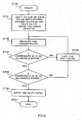
FIG.4 , processing will specifically be described below for drivingvoltage setting device 30 to record applied voltage values (minimum emission voltages) in applied voltage storage registers 11, 12 and 13 for respective colors and further record the duty ratio data in duty ratio storage registers 21, 22 and 23. - Driving
voltage setting device 30 starts the processing in step ST10, and in the subsequent step, ST11, sets duty ratios in dutyratio setting section 34. Since the case ofFIG.4 shows processing for setting a voltage to apply to the red LED, the settingdevice 30 sets the ON duty ratio of the red LED at a maximum value, while setting ON duty ratios of the green and blue LEDs at zero. In other words, PWMwaveform forming circuit 24 is given data with the ON duty ratio of the maximum value, while PWMwaveform forming circuits microcomputer 32 sets a target luminance. - In step ST13, applied
voltage setting section 33 sets a minimum applied voltage value Vmin (for example, 1.5V), andvoltage varying circuit 18 converts the voltage generated in power supplyvoltage generating circuit 19 into the set voltage to apply toLED unit 20. At this point, since only the red PWMwaveform forming circuit 24 outputs a PWM signal with the maximum ON duty ratio, the red LED is only in a state for enabling light emission. - In step ST14,
microcomputer 32 judges whether or not the measured luminance obtained by luminance/chromaticity meter 31 is greater than the target luminance. When the measured luminance is less than the target luminance,microcomputer 32 shifts to the processing of step S15, increases a set applied voltage in appliedvoltage setting section 33 by k (for example, 0.1V), and makes the judgment in step ST14 again. - A positive result obtained in step ST14 means that the minimum voltage required to obtain a desired luminance is currently being applied to the red LED, and the processing flow shifts to step ST16 where
microcomputer 32 writes the voltage value currently set in appliedvoltage setting section 33 in R applied voltage storage register 11. Thus, the minimum emission voltage value required for the red LED to obtain a desired luminance is stored in R applied voltage storage register 11. - In the subsequent step, ST17,
microcomputer 32 judges whether or not the measured luminance agrees with the target luminance. When agreement is not obtained,microcomputer 32 shifts to step ST18, decreases the ON duty ratio set in dutyratio setting section 32 by r, and returns to step ST17. - A positive result obtained in step ST17 means that it is possible to cause the red LED to emit light with the desired luminance using the PWM signal with the duty ratio currently set in duty
ratio setting section 34, and the processing flow shifts to step ST19 wheremicrocomputer 32 writes the duty ratio currently set in dutyratio setting section 34 in R dutyratio storage register 21. Thus, the duty ratio for the red LED to obtain the desired luminance is stored in R dutyratio storage register 21. - In other words, the processing of steps ST17 to STi9 indicates that the duty ratio is set to perform fine luminance control using the PWM signal so as to bring the luminance close to the target luminance after setting in steps ST14 to ST16 the minimum applied voltage enabling the target luminance to be obtained. In the subsequent step, ST20, driving
voltage setting device 30 finishes the processing for writing data in R applied voltage storage register 11 and R dutyratio storage register 21. - In addition, herein described is the processing for writing data in R applied voltage storage register 11 and R duty
ratio storage register 21, and similar procedures are carried out to perform processing for writing data in G and B applied voltage storage registers 12 and 13 and G and B duty ratio storage registers 22 and 23. - Referring to
FIG.5 , procedures will be described below to store in theregisters - Driving
voltage setting device 30 starts white balance adjustment processing in step ST30, and in the subsequent step, ST31, lights the LEDs of respective colors sequentially using applied voltages stored in applied voltage storage registers 11, 12 and 13 and PWM signals with duty ratios stored in duty ratio storage registers 21, 22 and 23, while drivingLCD panel 40 using the LCD driving circuit (not shown). - Actually,
LED driving device 10 applies voltages for the LEDs of respective colors stored in applied voltage storage registers 11, 12 and 13 sequentially toLED unit 20, and in synchronization with the voltage application, PWMwaveform forming circuits - In other words, in step ST31 is performed actual LED driving and LCD driving in the field sequential system. It is herein assumed that data stored in applied voltage storage registers 11, 12 and 13 and duty ratio storage registers 21, 22 and 23 is data set as shown in
FIG.4 . - In step S32, luminance/
chromaticity meter 31 measures the chromaticity of a display color.FIG.6 shows measured degrees of chromaticity plotted in the chromaticity space. Then,microcomputer 32 calculates a difference between the measured chromaticity and a target value of the white balance, and dutyratio setting section 34 corrects duty ratios to set corresponding to the difference to supply to PWMwaveform forming circuits Microcomputer 32 is capable of reading out duty ratios for respective colors stored in duty ratio storage registers 21, 22 and 23, and based on the read duty ratios for respective colors and the difference between the measured chromaticity and target value of the white balance, designates the duty ratios for respective colors to next set in dutyratio setting section 34. By this means, the duty ratios for respective colors are set at values such that the target white balance is obtained. - Specifically, it is first judged in step ST33 whether or not the Y coordinate of the measured chromaticity is within a white allowable range as shown in
FIG.6 , and it is further judged in step ST34 whether or not the X coordinate of the measured chromaticity is within the white allowable range as shown inFIG. 6 . When a negative result is obtained in either step ST33 or step ST34, the processing flow shifts to step ST35, and dutyratio setting section 34 corrects the duty ratio. - The correction of the duty ratio is made based on the difference in direction and scale between a target point of the white balance and the measured chromaticity. In the case of this embodiment,
microcomputer 32 considers a distribution range of chromaticity of the LED of each color, and corrects the duty ratio of the PWM signal for the LED of each color. For example, the amount of the difference is allocated in proportion to the amount of correction of the duty ratio for the LED of each color in consideration of the distribution range of chromaticity of the LED of each color, whereby it is possible to find the duty ratio such that the white balance falls within the allowable range promptly in a small number of corrections. - For example, as shown in
FIG. 6 , a case is considered where the Y coordinate of a measured value is larger than that of the target point, and that the X coordinate of the measured value is smaller than that of the target point. Respective distribution ranges of the LEDs of colors, R, G and B, in chromaticity space are generally as shown inFIG.6 . Therefore, in order to decrease the Y component and increase the X component to bring the white balance close to the target point, for example, the red ON duty ratio is increased, while the green ON duty ratio is decreased. - By thus setting ON duty ratios in proportional allocation as described below, it is possible to find respective duty ratios for the colors such that the target white balance is obtained a small number of settings.
- Obtaining positive results in both steps ST33 and ST34 mean that the white balance is in the white allowable range, and therefore, driving
voltage setting device 30 shifts to step ST36, stores duty ratios for red, green and blue currently set in dutyratio setting section 34 respectively in duty ratio storage registers 21, 22 and 23, and finishes the white balance adjustment processing in the subsequent step, ST37. - Thus, driving
voltage setting device 30 starts with the duty ratio such that a desired luminance is obtained on the LED of each of colors, R, G and B, independently, measures the white balance of the actual display color, corrects respective duty ratios for the colors corresponding to the measured values, while searching for duty ratios such that the desired white balance is obtained, and stores respective duty ratios for the colors at the time the desired white balance is obtained in corresponding duty ratio storage registers 21, 22 and 23. - In this way, driving
voltage setting device 30 corrects the duty ratio for each color, thereby makes an adjustment to the white balance, and therefore, is capable of adjusting the white balance finely with ease. Further, by storing duty ratios to adjust the white balance inwritable registers - The operation of
LED driving device 10 of this embodiment will be described below with reference toFIG. 7 . InLED driving device 10, in an red-LED emission period LR, register selectingcircuit 15 first selects an output of R applied voltage storage register 11 among from outputs of applied voltage storage registers 11, 12 and 13, andvoltage varying circuit 18 forms a voltage of 2.2V corresponding to the output of R applied voltage storage register 11, and supplies the voltage of 2.2V toLED unit 20 as shown inFIG.7(a) . - When the red-LED emission timing signal TR rises at time t2 during the red-LED emission period LR, PWM
waveform forming circuit 24 outputs a PWM signal with the duty ratio stored in R dutyratio storage register 21 totransistor 27, and thereby the red LED emits light in the luminance corresponding to the PWM signal. Then, when the red-LED emission timing signal TR falls at time t3, the output from PWMwaveform forming circuit 24 is halted, and register selectingcircuit 15 selects an output of G appliedvoltage storage register 12, substituting for the output of R applied voltage storage register 11. - By this means, in a green-LED emission period LG,
LED driving device 10 forms a voltage of 3.3V involtage varying circuit 18 corresponding to data of G appliedvoltage storage register 12, and supplies the voltage of 3. 3V toLED unit 20. When the green-LED emission timing signal TG rises at time t4 during the green-LED emission period LG, PWMwaveform forming circuit 25 outputs a PWM signal with the duty ratio stored in G dutyratio storage register 22 totransistor 28, and thereby the green LED emits light in the luminance corresponding to the PWM signal. Then, when the green-LED emission timing signal TG falls at time t5, the output from PWMwaveform forming circuit 25 is halted, and register selectingcircuit 15 selects an output of B appliedvoltage storage register 13, substituting for the output of G appliedvoltage storage register 12. - By this means, in a blue-LED emission period LB,
LED driving device 10 forms a voltage of 3.4V involtage varying circuit 18 corresponding to data of B appliedvoltage storage register 13, and supplies the voltage of 3. 4V toLED unit 20. When the blue-LED emission timing signal TB rises at time t6 during the blue-LED emission period LB, PWMwaveform forming circuit 26 outputs a PWM signal with the duty ratio stored in B dutyratio storage register 23 totransistor 29, and thereby the blue LED emits light in the luminance corresponding to the PWM signal. Then, when the blue-LED emission timing signal TB falls at time t7, the output from PWMwaveform forming circuit 26 is halted, and register selectingcircuit 15 selects an output of R applied voltage storage register 11, substituting for the output of B appliedvoltage storage register 13. - Thereafter, in the same way as the foregoing, repeated are the red-LED emission period LR, green-LED emission period LG and blue-LED emission period LB, whereby color display is carried out in the field sequential system.
- In addition, in the case of this embodiment, each of the LED emission periods LR, LG and LB is set at about 5mS, and the PWM signal output period for each color is set at about µ s. Further, a waveform of the PWM signal has a unit cycle of 50µ s, and the duty ratio in the unit cycle is stored in each of the duty ratio storage registers 21 to 23. In the case of this embodiment, duty ratios of eight bits (=256 different ratios) are stored in each of the duty ratio storage registers 21 to 23.
- Thus, according to this embodiment, the LED of each of colors, red, green and blue, undergoes PWM control independently during a unit emission period to emit light, luminance/
chromaticity meter 31 measures the chromaticity of the light emission, a difference is calculated between the measured value and target white balance value, the duty ratio for the LED of each of the colors is corrected corresponding to the difference to light the LED of each of the colors again, and the duty ratio for the LED of each of the colors such that the difference falls within a predetermined allowable range is stored in the dutyratio storage register LCD panel 40. - Further, rough luminance adjustment is first made by storing a minimum voltage value for each color when a luminance higher than a target is obtained in a state where the duty ratio is maximum, and fine luminance adjustment is then made by varying the duty ratio of the PWM signal while applying the stored applied voltage of fixed value, whereby current consumption can be reduced, in addition to the fact that white balance is adjusted with excellence.
- In addition, in the aforementioned embodiment, for simplicity in drawings and descriptions,
LED unit 20 is comprised of two red LEDs, two blue LEDs and one green LED, but the present invention is not limited to such the number of the LED of each color. Further, any number is available as the number ofLED units 20, and it may be possible to set the driving voltage and duty ratio of an LED of each color independently for each of the LED units to store in memory. - Moreover, it may be possible that a variable voltage is applied independently to each of LEDs of the same color, the luminance is detected independently on each of LEDs of the same color, a minimum applied voltage value when a luminance higher than a desired value is detected is set as a driving voltage value on each of LEDs of the same color and stored in applied
voltage storage register - Similarly, it may be possible that each of LEDs of the same color is controlled using the PWM signal with a different duty ratio, the duty ratio for each of the LEDs of the same color when a desired luminance and white balance is detected is stored independently in duty
ratio storage register - Further, the above-mentioned embodiment describes the case of using a liquid crystal display device in the field sequential system, but the present invention is not limited to such a case and widely applied to display devices to perform color display using LEDs of three colors, R, G and B. Furthermore, the above-mentioned embodiment describes the case of applying the independent voltage for each color to an LED of each color, but the present invention is not limited to such a case and enables the same effects to be obtained also in the case of applying the same voltage to the LED of each color.
- The present invention is not limited to the above-mentioned embodiment, and is capable of being carried into practice with various modifications thereof.
- An aspect of an adj ustment method of a display device of the present invention includes an LED emission step of performing PWM control independently on an LED of each of colors, red, green and blue, in a unit emission period to cause the LED to emit light, a measuring step of measuring chromaticity of the light, a calculating step of calculating a difference between a measured value obtained in the measuring step and a target white balance value, a correcting step of correcting a duty ratio of a PWM signal on the LED of each of colors in the LED emission step corresponding to the difference obtained in the calculating step, and a duty ratio storing step of storing a duty ratio for the LED of each of colors in a storage when the difference calculated in the calculating step falls within a predetermined allowable range.
- According to this method, emission in a unit emission period of the LED of each of colors is controlled using the PWM signal, while storing in the storage the duty ratio of the PWM signal for the LED of each of colors such that the white balance falls within an allowable range. Therefore, even when there are fluctuations between LEDs of the colors due to individual differences, it is possible to make a display adjustment with ease such that the white balance falls within an allowable range.
- In another aspect of the adjustment method of a display device of the present invention, the adjustment of the display device is made in such a state that an LCD panel is attached to a front face of the LED and that the LCD panel is driven.
- According to this method, even when there are fluctuations between LCD panels due to individual product differences, it is possible to absorb the fluctuations and bring the white balance into an allowable range.
- In still another aspect of the adjustment method of a display device of the present invention, in the correcting step, the duty ratio of the PWM signal for the LED of each of colors is corrected in consideration of a distribution range of the chromaticity of the LED of each of colors.
- According to this method, it is possible to find the duty ratio such that the white balance falls within the allowable range promptly in a small number of corrections. For example, the amount of the difference is allocated in proportion to the amount of correction of the duty ratio for the LED of each of colors in consideration of the distribution range of the chromaticity of the LED of each of colors.
- In still another aspect of the adjustment method of a display device of the present invention, the duty ratio is corrected independently on LEDs of the same color corresponding to the difference obtained in the calculating step, and independent duty ratios for the LEDs of the same color are stored in the duty ratio storing step.
- According to this method, it is possible to adjust the LEDs of the same color using independent PWM signals, and it is thereby possible to execute finer white balance adjustment processing than in the case of performing PWM control on the LEDs of the same color collectively using the same PWM signal.
- An aspect of a display device of the present invention adopts a configuration having a duty ratio storage which is comprised of writable memory and stores therein a duty ratio to perform PWM control independently on an LED of each of colors, red, green and blue, in a unit emission period, independently for each LED, a PWM controller which forms a PWM signal based on the duty ratio stored in the duty ratio storage independently for each LED to perform PWM control independently on the LED of each of colors in the unit emission period, and a signal line connected to the duty ratio storage to input the duty ratio to the duty ratio storage.
- Another aspect of the display device of the present invention adopts a configuration where the duty ratio storage stores the duty ratio provided with a white balance adjustment via the signal line.
- According to these configurations, emission in a unit emission period of the LED of each of colors is controlled using the PWM signal, and it is thereby possible to adjust the white balance finely with ease. Further, the duty ratio of the PWM signal for the LED of each of colors is stored in the writable memory, and it is thus possible to write the duty ratio adapted to the display device at any time.
- Still another aspect of the display device of the present invention adopts a configuration where the duty ratio storage stores independent duty ratios for LEDs of the same color, and the PWM controller forms independent PWM signals for the LEDs of the same color to perform PWM control independently on the LEDs of the same color in a unit emission control.
- According to this configuration, the LEDs of the same color are also controlled in emission using the independent PWM signals, and it is thus possible to perform finer white balance display.
- As described above, according to the present invention, emission in a unit emission period of the LED of each of colors is controlled using the PWM signal, while storing in the storage the duty ratio of the PWM signal for the LED of each of colors such that the white balance falls within an allowable range. Therefore, it is possible to implement an adjustment method of a display device and the display device enabling the white balance adjustment to be made finely with ease even when there are fluctuations in emission characteristics of LED and LCD panel.
- Further, rough luminance adjustment is first made by storing a minimum voltage value for each color when a luminance higher than a target is obtained in a state where the duty ratio is maximum, and fine luminance adjustment is then made by varying the duty ratio of the PWM signal while applying the stored applied voltage of fixed value, whereby current consumption can be reduced, in addition to the fact that the white balance is adjusted with excellence.
- The present invention is suitable for being applied to, for example, a liquid crystal display device.
- 10
- LED DRIVING DEVICE
- 11
- R APPLIED VOLTAGE STORAGE REGISTER
- 12
- G APPLIED VOLTAGE STORAGE REGISTER
- 13
- B APPLIED VOLTAGE STORAGE REGISTER
- 15
- REGISTER SELECTING CIRCUIT
- 17
- DA CONVERTING CIRCUIT
- 18
- VOLTAGE VARYING CIRCUIT
- 19
- POWER SUPPLY VOLTAGE GENERATING CIRCUIT
- 21
- R DUTY RATIO STORAGE REGISTER
- 22
- G DUTY RATIO STORAGE REGISTER
- 23
- B DUTY RATIO STORAGE REGISTER
- 24 25 26
- PWM WAVEFORM FORMING CIRCUIT
- MINIMUM VALUE STANDARD VALUE MAXIMUM VALUE
- RED LED GREEN LED BLUE LED
- 30
- DRIVING VOLTAGE SETTING DEVICE
- 31
- LUMINANCE/CHROMATICITY METER
- 32
- MICROCOMPUTER
- 33
- APPLIED VOLTAGE SETTING SECTION
- 34
- DUTY RATIO SETTING SECTION
- 40
- LCD PANEL
- ST10
- START
- ST11
- SET ON DUTY RATIOS R: MAXIMUM
- ST12
- SET THE TARGET LUMINANCE
- ST13
- APPLY VOLTAGE Vmin
- ST14
- MEASURED LUMINANCE>TARGET LUMINANCE ?
- ST16
- STORE THE APPLIED VOLTAGE VALUE
- ST17
- MEASURED LUMINANCE=TARGET LUMINANCE ?
- ST19
- STORE THE ON DUTY RATIOS
- ST20
- END
- ST30
- START
- ST31
- LIGHT AN LED OF EACH COLOR WITH STORED APPLIED VOLTAGE AND DUTY RATIO. DRIVE THE LIQUID CRYSTAL
- ST32
- MEASURE THE CHROMATICITY
- ST33
- Y COORDINATE IS IN AN ALLOWABLE RANGE ?
- ST34
- X COORDINATE IS IN AN ALLOWABLE RANGE ?
- ST35
- VARY THE DUTY RATIO
- ST36
- WRITE THE DUTY RATIO
- ST37
- END
- ELEMENT CHROMATICITY RANGE
- Green LED DISTRIBUTION RANGE
- Blue LED DISTRIBUTION RANGE
- Red LED DISTRIBUTION RANGE
- RGB PWM VALUE FINE ADJUSTMENT DIRECTION
- WHITE ALLOWABLE RANGE
Claims (5)
- An adjustment method of a display device, comprising:a) an applied voltage setting step of performing a rough luminance adjustment by applying (ST13) an voltage to an LED (20) of one (R) of colors (R, G, B), red (R), green (G) and blue (B), measuring (ST14) an emission luminance of the LED (20) of the one (R) of the colors (R, G, B), increasing (ST15) the applied voltage by voltage steps of k until said measured emission luminance is higher than a target luminance, then stopping the incrementation and storing (ST16) the incremented voltage value in registers;b) a duty ratio setting step of performing a fine luminance adjustment by fixedly applying the voltage set in the applied voltage setting step to the LED (20) of the one (R) of the colors (R, G, B), measuring (ST17) an emission luminance of the LED (20) of the one (R) of the colors (R, G, B), varying a duty ratio of a PWM signal performing switching control of the LED (20) of the one (R) of the colors (R, G, B) and storing (ST19) a duty ratio in the registers when the target luminance of the one (R) of the colors (R, G, B) is obtained;c) performing the steps a) and b) for each color of the colors (R, G, B);d) an LED emission step (ST31) of performing PWM control independently on an LED (20) of each of the colors (R, G, B), red (R), green (G) and blue (B), in a unit emission period to cause the LED (20) to emit light, wherein the applied voltage values and duty ratios stored in the registers are loaded;e) a measuring step (ST32) of measuring chromaticity of the light;f) a calculating step (ST33, ST34) of calculating a difference between a measured value obtained in the measuring step (ST32) and a target white balance value;g) a PWM signal correcting step (ST35) of correcting a duty ratio of a PWM signal on the LED (20) of each of the colors (R, G, B) in the LED emission step (ST31) corresponding to the difference obtained in the calculating step (ST33, ST34); andh) a duty ratio storing step (ST36) of storing a duty ratio for the LED (20) of each of the colors (R, G, B) in the registers when the difference calculated in the calculating step falls within a predetermined allowable range,wherein:the series of the LED emission step (ST31), measuring step (ST32), calculating step (ST33, ST34), PWM signal correcting step (ST35), duty ratio storing step (ST36) provide a duty ratio correcting step of fixedly applying the voltage set in the applied voltage setting step, changing the duty ratio set in the duty ratio setting step, measuring the white balance when the LED (20) of each color (R, G, B) is emitted, and storing (ST36) the duty ratio for each color (R, G, B) when a target white balance is achieved;the duty ratio of the PWM signal for the LED (20) of each of the colors (R, G, B) is corrected (ST35) in consideration of a distribution range of the chromaticity of the LED (20) of colors (R, G, B); andthe correction of the duty ratio is made based on the difference between a target point of the white balance and the measured chromaticity.
- The method according to claim 1, wherein an adjustment of the display device is made in such a state that an LCD panel is attached to a front face of the LED (20) and that the LCD panel is driven.
- The method according to claim 1, wherein the duty ratio is corrected independently on LED (20) of the same color corresponding to the difference obtained in the calculating step (ST33, ST34), and independent duty ratios for the LED (20) of the same color are stored in the duty ratio storing step (ST36).
- A display device comprising:LED (20) of colors (R, G, B) red (R), green (G) and blue (B) configured to emit light;a duty ratio storage (21, 22, 23) which is comprised of writable memory and is configured to store therein a duty ratio to perform PWM control independently on an LED (20) of each of colors (R, G, B), red (R), green (G) and blue (B), in a unit emission period, independently for each LED (20);a PWM controller (24, 25, 26) configured to form a PWM signal based on the duty ratio stored in the duty ratio storage (21, 22, 23) independently for each LED (20) to perform PWM control independently on the LED (20) of each of colors (R, G, B) in the unit emission period; anda signal line (14) connected to the duty ratio storage (21, 22, 23) to input the duty ratio to the duty ratio storage (21, 22, 23),a chromaticity meter (31) configured to measure the chromaticity of the light;a microcomputer (32) configured to calculate a difference between a measured value obtained from the chromaticity meter (31) and a target white balance value;wherein the microcomputer (32) is further configured to correct a duty ratio of a PWM signal on the LED (20) of each of colors (R, G, B) in the LED emission period corresponding to the difference calculated by the microcomputer (32), and to store a duty ratio for the LED (20) of each of colors (R, G; B) in the duty ratio storage (21, 22, 23) when the difference calculated by the microcomputer (32) falls within a predetermined allowable range;
characterized by:an applied voltage storage (11, 12, 13) configured to store an applied voltage value for each independent color (R, G, B); wherein:the microcomputer (32) is further configured to perform a rough luminance adjustment by applying an voltage to an LED (20) of one (R) of colors (R, G, B), red (R), green (G) and blue (B), to measure an emission luminance of the LED (20) of the one (R) of the colors (R, G, B), to increase the applied voltage by voltage steps of k until the measured emission luminance is higher than a target luminance, then stopping the incrementation and to store the incremented voltage in the applied voltage storage (11, 12,13);the microcomputer (32) is further configured to perform a fine luminance adjustment by fixedly applying the voltage set in the rough luminance adjustment period to the LED (20) of the one (R) of the colors (R, G, B), to measure (ST17) an emission luminance of the LED (20) of the one (R) of the colors (R, G, B), varying a duty ratio of the PWM signal performing switching control of the LED (20) of the one (R) of the colors (R, G, B) and to store a duty ratio in the duty ratio storage (21, 22, 23) when the target luminance of the one (R) of the colors (R, G, B) is obtained;the microcomputer (32) is further configured to correct the duty ratio of the PWM signal for the LED (20) of each of colors (R, G, B) in consideration of a distribution of the chromaticity of the LED (20) of each of colors (R, G, B); andthe microcomputer (32) is further configured to make the correction of the duty ratio based on the difference between a target point of the white balance and the measured chromaticity. - The device according to claim 4, wherein the duty ratio storage (21, 22, 23) is configured to store independent duty ratios for LED (20) of the same color, and the PWM controller (32) is further configured to form independent PWM signals for the LED (20) of the same color to perform PWM control independently on the LED (20) of the same color in a unit emission control.
Applications Claiming Priority (3)
| Application Number | Priority Date | Filing Date | Title |
|---|---|---|---|
| JP2003098488AJP2004309509A (en) | 2003-04-01 | 2003-04-01 | Method for adjusting display device |
| JP2003098488 | 2003-04-01 | ||
| PCT/JP2004/004291WO2004090856A1 (en) | 2003-04-01 | 2004-03-26 | Display device adjusting method and display device |
Publications (3)
| Publication Number | Publication Date |
|---|---|
| EP1562170A1 EP1562170A1 (en) | 2005-08-10 |
| EP1562170A4 EP1562170A4 (en) | 2005-12-07 |
| EP1562170B1true EP1562170B1 (en) | 2008-11-19 |
Family
ID=33156673
Family Applications (1)
| Application Number | Title | Priority Date | Filing Date |
|---|---|---|---|
| EP04723725AExpired - LifetimeEP1562170B1 (en) | 2003-04-01 | 2004-03-26 | Display device adjusting method and display device |
Country Status (9)
| Country | Link |
|---|---|
| US (1) | US20060152468A1 (en) |
| EP (1) | EP1562170B1 (en) |
| JP (1) | JP2004309509A (en) |
| KR (1) | KR100676238B1 (en) |
| CN (1) | CN1701350A (en) |
| AT (1) | ATE414973T1 (en) |
| DE (1) | DE602004017832D1 (en) |
| TW (1) | TW200424996A (en) |
| WO (1) | WO2004090856A1 (en) |
Families Citing this family (64)
| Publication number | Priority date | Publication date | Assignee | Title |
|---|---|---|---|---|
| US7139595B2 (en)* | 2002-10-24 | 2006-11-21 | The Rail Network, Inc. | Transit vehicle wireless transmission broadcast system |
| US7425801B2 (en)* | 2003-04-01 | 2008-09-16 | Hunet Display Technology Inc. | LED driving device for multiple color LED displays |
| KR100659531B1 (en) | 2003-11-27 | 2006-12-19 | 삼성에스디아이 주식회사 | Backlight driving circuit |
| KR100985858B1 (en) | 2004-04-27 | 2010-10-08 | 삼성전자주식회사 | LCD Display |
| JP2005321727A (en)* | 2004-05-11 | 2005-11-17 | Sony Corp | Backlight device and color liquid crystal display |
| EP1770416B1 (en)* | 2004-07-15 | 2012-02-22 | Sony Corporation | Color filter and color liquid crystal display device |
| JP4815781B2 (en)* | 2004-10-20 | 2011-11-16 | ソニー株式会社 | Color liquid crystal display device and backlight device |
| KR100713889B1 (en)* | 2004-12-22 | 2007-05-04 | 비오이 하이디스 테크놀로지 주식회사 | Backlight drive circuit |
| KR100752376B1 (en)* | 2005-02-22 | 2007-08-27 | 삼성에스디아이 주식회사 | Backlight driving circuit and liquid crystal display device having same |
| DE102005020568A1 (en)* | 2005-04-30 | 2006-11-09 | Osram Opto Semiconductors Gmbh | Light source arrangement for backlighting of display devices and display device |
| JP4428296B2 (en)* | 2005-06-10 | 2010-03-10 | セイコーエプソン株式会社 | Display panel module and display device |
| KR100714427B1 (en)* | 2005-10-12 | 2007-05-07 | 삼성전자주식회사 | Display device and control method |
| JP2007141738A (en)* | 2005-11-21 | 2007-06-07 | Sharp Corp | LIGHTING DEVICE, LIQUID CRYSTAL DISPLAY DEVICE, LIGHTING DEVICE CONTROL METHOD, LIGHTING DEVICE CONTROL PROGRAM, AND RECORDING MEDIUM |
| KR200416914Y1 (en)* | 2006-02-22 | 2006-05-23 | 김두일 | Driver to control polymer organic light emitting display |
| JP2007235050A (en)* | 2006-03-03 | 2007-09-13 | Sony Corp | Driving method for plane-like light source device, driving method of color liquid display device assembly, driving method of light emitting diode, and pulse modulation method |
| TWI371013B (en) | 2006-03-29 | 2012-08-21 | Au Optronics Corp | Liquid crystal device, method for displaying color images, and method for controlling light sources of a liquid crystal panel |
| KR100691628B1 (en)* | 2006-04-07 | 2007-03-12 | 삼성전기주식회사 | LED array driving device |
| CN100552765C (en)* | 2006-04-25 | 2009-10-21 | 友达光电股份有限公司 | Liquid crystal display, color image display method and method for controlling light source |
| JP4182989B2 (en) | 2006-05-30 | 2008-11-19 | ソニー株式会社 | Illumination device and liquid crystal display device |
| US7696964B2 (en)* | 2006-06-09 | 2010-04-13 | Philips Lumileds Lighting Company, Llc | LED backlight for LCD with color uniformity recalibration over lifetime |
| JP2008076899A (en)* | 2006-09-22 | 2008-04-03 | Sony Corp | Backlight device and display device |
| US8373355B2 (en)* | 2006-11-09 | 2013-02-12 | Apple Inc. | Brightness control of a status indicator light |
| US8531382B2 (en)* | 2006-11-29 | 2013-09-10 | Sharp Kabushiki Kaisha | White LED backlight device with color compensation and display device using the same |
| US20090167193A1 (en)* | 2006-11-29 | 2009-07-02 | Panasonic Corporation | Image-processing equipments, image-processing method, program, and recording medium |
| JP4285532B2 (en)* | 2006-12-01 | 2009-06-24 | ソニー株式会社 | Backlight control device, backlight control method, and liquid crystal display device |
| KR101370339B1 (en) | 2006-12-04 | 2014-03-05 | 삼성전자 주식회사 | Back Light Apparatus And Control Method Thereof |
| KR100831871B1 (en)* | 2006-12-05 | 2008-05-22 | 엘지이노텍 주식회사 | LED backlight control circuit |
| JP2008158454A (en)* | 2006-12-26 | 2008-07-10 | Sony Corp | Liquid crystal display device |
| JP4264560B2 (en)* | 2007-01-24 | 2009-05-20 | ソニー株式会社 | Backlight device, backlight control method, and liquid crystal display device |
| KR101385453B1 (en)* | 2007-05-02 | 2014-04-21 | 삼성디스플레이 주식회사 | Driving method of light source and back light assembly for carrying out the driving method |
| US8044899B2 (en)* | 2007-06-27 | 2011-10-25 | Hong Kong Applied Science and Technology Research Institute Company Limited | Methods and apparatus for backlight calibration |
| JP2009020385A (en)* | 2007-07-13 | 2009-01-29 | Seiko Epson Corp | Electro-optical device, control method thereof, and electronic apparatus |
| KR101443371B1 (en)* | 2007-07-13 | 2014-09-29 | 엘지디스플레이 주식회사 | Liquid crystal display and driving method thereof |
| JP4455620B2 (en) | 2007-07-17 | 2010-04-21 | 東芝モバイルディスプレイ株式会社 | Display device manufacturing method and color balance adjusting method |
| KR101503309B1 (en)* | 2007-12-06 | 2015-03-17 | 엘지디스플레이 주식회사 | Apparatus for compensating for color back light unit |
| JP2009168927A (en)* | 2008-01-11 | 2009-07-30 | Hitachi Displays Ltd | Organic EL display device |
| KR101511127B1 (en)* | 2008-01-22 | 2015-04-10 | 삼성디스플레이 주식회사 | Light source driving method, light source driving device and display device having same |
| JP5642347B2 (en)* | 2008-03-07 | 2014-12-17 | ミツミ電機株式会社 | LCD backlight device |
| JPWO2009116637A1 (en)* | 2008-03-19 | 2011-07-21 | 旭硝子株式会社 | Image display device having function of transmitting light from object to be observed |
| DE102008018808A1 (en)* | 2008-04-15 | 2009-10-22 | Ledon Lighting Jennersdorf Gmbh | Microcontroller optimized pulse width modulation (PWM) control of a light emitting diode (LED) |
| JP2009276672A (en)* | 2008-05-16 | 2009-11-26 | Canon Inc | Display device |
| KR101573434B1 (en)* | 2008-12-02 | 2015-12-02 | 삼성디스플레이 주식회사 | A light source driving method, a light source device for performing the same, and a display device having the light source device |
| TWI406229B (en)* | 2008-12-16 | 2013-08-21 | Chunghwa Picture Tubes Ltd | Light source display displayed by color sequent |
| CN101860764B (en)* | 2009-04-08 | 2012-07-18 | 鸿富锦精密工业(深圳)有限公司 | White balance adjustment method |
| JP5235993B2 (en)* | 2009-06-03 | 2013-07-10 | 三菱電機株式会社 | Image display device |
| CN102034441B (en)* | 2009-09-29 | 2013-05-08 | 深圳Tcl新技术有限公司 | LCD drive voltage control device |
| KR20110057456A (en)* | 2009-11-24 | 2011-06-01 | 삼성전자주식회사 | Display device and backlight unit |
| TWI465152B (en)* | 2010-06-28 | 2014-12-11 | Hon Hai Prec Ind Co Ltd | Led display device capable of balancing its current and method thereof |
| CN102014554B (en)* | 2010-09-28 | 2013-07-10 | 深圳市明微电子股份有限公司 | Method and device for adjusting drive current |
| CN101996585A (en)* | 2010-11-03 | 2011-03-30 | 中航华东光电有限公司 | RGB three primary colours LED backlight based automatic white balance adjustment system and method thereof |
| CN102646395B (en)* | 2012-04-27 | 2015-06-10 | 京东方科技集团股份有限公司 | Control device and control method of direct beck light source |
| TWI467550B (en)* | 2012-08-15 | 2015-01-01 | Novatek Microelectronics Corp | Backlight module and driving method thereof |
| CN103594062A (en)* | 2012-08-17 | 2014-02-19 | 联咏科技股份有限公司 | Backlight module and driving method thereof |
| CN103021379B (en)* | 2012-12-25 | 2015-10-07 | 广东威创视讯科技股份有限公司 | Based on color calibration method and the system of customization light source duty ratio |
| JP6322440B2 (en)* | 2013-03-06 | 2018-05-09 | 矢崎総業株式会社 | Color control method |
| DE102013220397A1 (en) | 2013-10-10 | 2015-04-16 | Ruling Technologies Sdn. Bhd. | Method and control device for operating at least one light source |
| KR102106271B1 (en) | 2013-10-24 | 2020-05-06 | 삼성디스플레이 주식회사 | Display apparatus and driving method thereof |
| CN103730096B (en)* | 2013-12-31 | 2016-09-14 | 深圳市华星光电技术有限公司 | White balance adjustment method and system, liquid crystal display manufacture method |
| CN104766574B (en)* | 2015-03-24 | 2019-02-12 | 小米科技有限责任公司 | Color temperature adjustment method and device |
| KR20200057256A (en)* | 2018-11-16 | 2020-05-26 | 삼성전자주식회사 | Display apparatus and driving method thereof |
| CN110379375B (en)* | 2019-06-25 | 2021-05-07 | 深圳市金锐显数码科技有限公司 | Automatic switching method and automatic switching system for backlight current gears |
| CN111800916A (en)* | 2020-06-24 | 2020-10-20 | 苏州浪潮智能科技有限公司 | System and method for calibrating colors of port lamps of data center switch |
| US11835382B2 (en) | 2021-03-02 | 2023-12-05 | Apple Inc. | Handheld electronic device |
| US12355907B2 (en) | 2022-01-10 | 2025-07-08 | Apple Inc. | Handheld electronic device |
Citations (1)
| Publication number | Priority date | Publication date | Assignee | Title |
|---|---|---|---|---|
| JP2000111871A (en)* | 1998-10-02 | 2000-04-21 | Canon Inc | Color liquid crystal display |
Family Cites Families (9)
| Publication number | Priority date | Publication date | Assignee | Title |
|---|---|---|---|---|
| US5724062A (en)* | 1992-08-05 | 1998-03-03 | Cree Research, Inc. | High resolution, high brightness light emitting diode display and method and producing the same |
| JPH09292601A (en)* | 1996-04-25 | 1997-11-11 | Kansei Corp | Liquid crystal display device |
| JP4050802B2 (en)* | 1996-08-02 | 2008-02-20 | シチズン電子株式会社 | Color display device |
| US6342897B1 (en)* | 1999-12-16 | 2002-01-29 | Dynascan Technology Corporation | Method and system for compensating for non-uniform color appearance of a display due to variations of primary colors |
| JP2002117999A (en)* | 2000-10-11 | 2002-04-19 | Sanyo Electric Co Ltd | Light dimming device and liquid crystal display using the same |
| FI109632B (en)* | 2000-11-06 | 2002-09-13 | Nokia Corp | White lighting |
| US7088334B2 (en)* | 2001-06-28 | 2006-08-08 | Matsushita Electric Industrial Co., Ltd. | Liquid crystal display device and manufacturing method thereof, and drive control method of lighting unit |
| JP2003029235A (en)* | 2001-07-17 | 2003-01-29 | Dainippon Printing Co Ltd | Field sequential liquid crystal display |
| JP4073272B2 (en)* | 2002-08-29 | 2008-04-09 | シチズン電子株式会社 | Color display device and white balance adjustment method for color display device |
- 2003
- 2003-04-01JPJP2003098488Apatent/JP2004309509A/enactivePending
- 2004
- 2004-03-26CNCNA2004800011212Apatent/CN1701350A/enactivePending
- 2004-03-26DEDE602004017832Tpatent/DE602004017832D1/ennot_activeExpired - Lifetime
- 2004-03-26USUS10/532,240patent/US20060152468A1/ennot_activeAbandoned
- 2004-03-26KRKR1020057007217Apatent/KR100676238B1/ennot_activeExpired - Fee Related
- 2004-03-26EPEP04723725Apatent/EP1562170B1/ennot_activeExpired - Lifetime
- 2004-03-26ATAT04723725Tpatent/ATE414973T1/ennot_activeIP Right Cessation
- 2004-03-26WOPCT/JP2004/004291patent/WO2004090856A1/enactiveApplication Filing
- 2004-03-30TWTW093108678Apatent/TW200424996A/ennot_activeIP Right Cessation
Patent Citations (1)
| Publication number | Priority date | Publication date | Assignee | Title |
|---|---|---|---|---|
| JP2000111871A (en)* | 1998-10-02 | 2000-04-21 | Canon Inc | Color liquid crystal display |
Non-Patent Citations (1)
| Title |
|---|
| PATENT ABSTRACTS OF JAPAN* |
Also Published As
| Publication number | Publication date |
|---|---|
| JP2004309509A (en) | 2004-11-04 |
| DE602004017832D1 (en) | 2009-01-02 |
| US20060152468A1 (en) | 2006-07-13 |
| ATE414973T1 (en) | 2008-12-15 |
| CN1701350A (en) | 2005-11-23 |
| EP1562170A4 (en) | 2005-12-07 |
| TW200424996A (en) | 2004-11-16 |
| TWI295045B (en) | 2008-03-21 |
| KR20060030847A (en) | 2006-04-11 |
| WO2004090856A1 (en) | 2004-10-21 |
| KR100676238B1 (en) | 2007-01-30 |
| EP1562170A1 (en) | 2005-08-10 |
Similar Documents
| Publication | Publication Date | Title |
|---|---|---|
| EP1562170B1 (en) | Display device adjusting method and display device | |
| TWI283844B (en) | Light emitting diode driver and light emitting diode driving method | |
| CN100514427C (en) | A scanning backlight for a matrix display | |
| US7622697B2 (en) | Brightness control for dynamic scanning backlight | |
| US7609240B2 (en) | Light generating device, display apparatus having the same and method of driving the same | |
| US7548030B2 (en) | Color control for dynamic scanning backlight | |
| KR101963784B1 (en) | Apparatus and method for driving back light, liquid crystal display device and driving method the same | |
| US20030214725A1 (en) | Color display device | |
| US7982827B2 (en) | System and method for dynamically altering a color gamut | |
| US20100097412A1 (en) | Light source device and liquid crystal display unit | |
| KR20120002704A (en) | Driving device of liquid crystal display and driving method thereof | |
| US20100066713A1 (en) | Image display | |
| JP4076083B2 (en) | LED driving voltage setting device and method | |
| KR101423112B1 (en) | Light generating device, display device having the same, and driving method thereof | |
| US11183108B2 (en) | System and method for reducing motion blur for LED display | |
| JP4015965B2 (en) | LED driving device and LED driving method | |
| JP2005184020A (en) | LED driving device and LED driving method | |
| JP2004309510A (en) | Device and method for driving led | |
| KR100831871B1 (en) | LED backlight control circuit | |
| HK1083274B (en) | Led drive device | |
| HK1083263A (en) | Display device adjusting method and display device |
Legal Events
| Date | Code | Title | Description |
|---|---|---|---|
| PUAI | Public reference made under article 153(3) epc to a published international application that has entered the european phase | Free format text:ORIGINAL CODE: 0009012 | |
| 17P | Request for examination filed | Effective date:20050428 | |
| AK | Designated contracting states | Kind code of ref document:A1 Designated state(s):AT BE BG CH CY CZ DE DK EE ES FI FR GB GR HU IE IT LI LU MC NL PL PT RO SE SI SK TR | |
| AX | Request for extension of the european patent | Extension state:AL LT LV MK | |
| A4 | Supplementary search report drawn up and despatched | Effective date:20051026 | |
| DAX | Request for extension of the european patent (deleted) | ||
| 17Q | First examination report despatched | Effective date:20060316 | |
| RAP1 | Party data changed (applicant data changed or rights of an application transferred) | Owner name:HUNET DISPLAY TECHNOLOGY INC. | |
| 17Q | First examination report despatched | Effective date:20060316 | |
| GRAP | Despatch of communication of intention to grant a patent | Free format text:ORIGINAL CODE: EPIDOSNIGR1 | |
| GRAS | Grant fee paid | Free format text:ORIGINAL CODE: EPIDOSNIGR3 | |
| GRAA | (expected) grant | Free format text:ORIGINAL CODE: 0009210 | |
| AK | Designated contracting states | Kind code of ref document:B1 Designated state(s):AT BE BG CH CY CZ DE DK EE ES FI FR GB GR HU IE IT LI LU MC NL PL PT RO SE SI SK TR | |
| REG | Reference to a national code | Ref country code:GB Ref legal event code:FG4D | |
| REG | Reference to a national code | Ref country code:CH Ref legal event code:EP | |
| REG | Reference to a national code | Ref country code:IE Ref legal event code:FG4D | |
| REF | Corresponds to: | Ref document number:602004017832 Country of ref document:DE Date of ref document:20090102 Kind code of ref document:P | |
| PG25 | Lapsed in a contracting state [announced via postgrant information from national office to epo] | Ref country code:AT Free format text:LAPSE BECAUSE OF FAILURE TO SUBMIT A TRANSLATION OF THE DESCRIPTION OR TO PAY THE FEE WITHIN THE PRESCRIBED TIME-LIMIT Effective date:20081119 Ref country code:ES Free format text:LAPSE BECAUSE OF FAILURE TO SUBMIT A TRANSLATION OF THE DESCRIPTION OR TO PAY THE FEE WITHIN THE PRESCRIBED TIME-LIMIT Effective date:20090301 | |
| NLV1 | Nl: lapsed or annulled due to failure to fulfill the requirements of art. 29p and 29m of the patents act | ||
| PG25 | Lapsed in a contracting state [announced via postgrant information from national office to epo] | Ref country code:PL Free format text:LAPSE BECAUSE OF FAILURE TO SUBMIT A TRANSLATION OF THE DESCRIPTION OR TO PAY THE FEE WITHIN THE PRESCRIBED TIME-LIMIT Effective date:20081119 Ref country code:NL Free format text:LAPSE BECAUSE OF FAILURE TO SUBMIT A TRANSLATION OF THE DESCRIPTION OR TO PAY THE FEE WITHIN THE PRESCRIBED TIME-LIMIT Effective date:20081119 Ref country code:SI Free format text:LAPSE BECAUSE OF FAILURE TO SUBMIT A TRANSLATION OF THE DESCRIPTION OR TO PAY THE FEE WITHIN THE PRESCRIBED TIME-LIMIT Effective date:20081119 Ref country code:FI Free format text:LAPSE BECAUSE OF FAILURE TO SUBMIT A TRANSLATION OF THE DESCRIPTION OR TO PAY THE FEE WITHIN THE PRESCRIBED TIME-LIMIT Effective date:20081119 | |
| PG25 | Lapsed in a contracting state [announced via postgrant information from national office to epo] | Ref country code:BE Free format text:LAPSE BECAUSE OF FAILURE TO SUBMIT A TRANSLATION OF THE DESCRIPTION OR TO PAY THE FEE WITHIN THE PRESCRIBED TIME-LIMIT Effective date:20081119 Ref country code:DK Free format text:LAPSE BECAUSE OF FAILURE TO SUBMIT A TRANSLATION OF THE DESCRIPTION OR TO PAY THE FEE WITHIN THE PRESCRIBED TIME-LIMIT Effective date:20081119 Ref country code:EE Free format text:LAPSE BECAUSE OF FAILURE TO SUBMIT A TRANSLATION OF THE DESCRIPTION OR TO PAY THE FEE WITHIN THE PRESCRIBED TIME-LIMIT Effective date:20081119 Ref country code:RO Free format text:LAPSE BECAUSE OF FAILURE TO SUBMIT A TRANSLATION OF THE DESCRIPTION OR TO PAY THE FEE WITHIN THE PRESCRIBED TIME-LIMIT Effective date:20081119 Ref country code:BG Free format text:LAPSE BECAUSE OF FAILURE TO SUBMIT A TRANSLATION OF THE DESCRIPTION OR TO PAY THE FEE WITHIN THE PRESCRIBED TIME-LIMIT Effective date:20090219 | |
| PG25 | Lapsed in a contracting state [announced via postgrant information from national office to epo] | Ref country code:PT Free format text:LAPSE BECAUSE OF FAILURE TO SUBMIT A TRANSLATION OF THE DESCRIPTION OR TO PAY THE FEE WITHIN THE PRESCRIBED TIME-LIMIT Effective date:20090420 Ref country code:SE Free format text:LAPSE BECAUSE OF FAILURE TO SUBMIT A TRANSLATION OF THE DESCRIPTION OR TO PAY THE FEE WITHIN THE PRESCRIBED TIME-LIMIT Effective date:20090219 Ref country code:CZ Free format text:LAPSE BECAUSE OF FAILURE TO SUBMIT A TRANSLATION OF THE DESCRIPTION OR TO PAY THE FEE WITHIN THE PRESCRIBED TIME-LIMIT Effective date:20081119 | |
| PLBE | No opposition filed within time limit | Free format text:ORIGINAL CODE: 0009261 | |
| STAA | Information on the status of an ep patent application or granted ep patent | Free format text:STATUS: NO OPPOSITION FILED WITHIN TIME LIMIT | |
| PG25 | Lapsed in a contracting state [announced via postgrant information from national office to epo] | Ref country code:SK Free format text:LAPSE BECAUSE OF FAILURE TO SUBMIT A TRANSLATION OF THE DESCRIPTION OR TO PAY THE FEE WITHIN THE PRESCRIBED TIME-LIMIT Effective date:20081119 | |
| 26N | No opposition filed | Effective date:20090820 | |
| PG25 | Lapsed in a contracting state [announced via postgrant information from national office to epo] | Ref country code:MC Free format text:LAPSE BECAUSE OF NON-PAYMENT OF DUE FEES Effective date:20090331 | |
| REG | Reference to a national code | Ref country code:CH Ref legal event code:PL | |
| REG | Reference to a national code | Ref country code:FR Ref legal event code:ST Effective date:20091130 | |
| REG | Reference to a national code | Ref country code:IE Ref legal event code:MM4A | |
| PG25 | Lapsed in a contracting state [announced via postgrant information from national office to epo] | Ref country code:LI Free format text:LAPSE BECAUSE OF NON-PAYMENT OF DUE FEES Effective date:20090331 Ref country code:IE Free format text:LAPSE BECAUSE OF NON-PAYMENT OF DUE FEES Effective date:20090326 Ref country code:CH Free format text:LAPSE BECAUSE OF NON-PAYMENT OF DUE FEES Effective date:20090331 | |
| PG25 | Lapsed in a contracting state [announced via postgrant information from national office to epo] | Ref country code:FR Free format text:LAPSE BECAUSE OF NON-PAYMENT OF DUE FEES Effective date:20091123 | |
| PG25 | Lapsed in a contracting state [announced via postgrant information from national office to epo] | Ref country code:GR Free format text:LAPSE BECAUSE OF FAILURE TO SUBMIT A TRANSLATION OF THE DESCRIPTION OR TO PAY THE FEE WITHIN THE PRESCRIBED TIME-LIMIT Effective date:20090220 | |
| PG25 | Lapsed in a contracting state [announced via postgrant information from national office to epo] | Ref country code:IT Free format text:LAPSE BECAUSE OF FAILURE TO SUBMIT A TRANSLATION OF THE DESCRIPTION OR TO PAY THE FEE WITHIN THE PRESCRIBED TIME-LIMIT Effective date:20081119 | |
| PG25 | Lapsed in a contracting state [announced via postgrant information from national office to epo] | Ref country code:LU Free format text:LAPSE BECAUSE OF NON-PAYMENT OF DUE FEES Effective date:20090326 | |
| PG25 | Lapsed in a contracting state [announced via postgrant information from national office to epo] | Ref country code:HU Free format text:LAPSE BECAUSE OF FAILURE TO SUBMIT A TRANSLATION OF THE DESCRIPTION OR TO PAY THE FEE WITHIN THE PRESCRIBED TIME-LIMIT Effective date:20090520 | |
| PG25 | Lapsed in a contracting state [announced via postgrant information from national office to epo] | Ref country code:TR Free format text:LAPSE BECAUSE OF FAILURE TO SUBMIT A TRANSLATION OF THE DESCRIPTION OR TO PAY THE FEE WITHIN THE PRESCRIBED TIME-LIMIT Effective date:20081119 | |
| PG25 | Lapsed in a contracting state [announced via postgrant information from national office to epo] | Ref country code:CY Free format text:LAPSE BECAUSE OF FAILURE TO SUBMIT A TRANSLATION OF THE DESCRIPTION OR TO PAY THE FEE WITHIN THE PRESCRIBED TIME-LIMIT Effective date:20081119 | |
| PGFP | Annual fee paid to national office [announced via postgrant information from national office to epo] | Ref country code:DE Payment date:20130321 Year of fee payment:10 | |
| PGFP | Annual fee paid to national office [announced via postgrant information from national office to epo] | Ref country code:GB Payment date:20140319 Year of fee payment:11 | |
| REG | Reference to a national code | Ref country code:DE Ref legal event code:R119 Ref document number:602004017832 Country of ref document:DE | |
| REG | Reference to a national code | Ref country code:DE Ref legal event code:R119 Ref document number:602004017832 Country of ref document:DE Effective date:20141001 | |
| PG25 | Lapsed in a contracting state [announced via postgrant information from national office to epo] | Ref country code:DE Free format text:LAPSE BECAUSE OF NON-PAYMENT OF DUE FEES Effective date:20141001 | |
| GBPC | Gb: european patent ceased through non-payment of renewal fee | Effective date:20150326 | |
| PG25 | Lapsed in a contracting state [announced via postgrant information from national office to epo] | Ref country code:GB Free format text:LAPSE BECAUSE OF NON-PAYMENT OF DUE FEES Effective date:20150326 |