EP1550105B1 - Transparent digitiser - Google Patents
Transparent digitiserDownload PDFInfo
- Publication number
- EP1550105B1 EP1550105B1EP03791166AEP03791166AEP1550105B1EP 1550105 B1EP1550105 B1EP 1550105B1EP 03791166 AEP03791166 AEP 03791166AEP 03791166 AEP03791166 AEP 03791166AEP 1550105 B1EP1550105 B1EP 1550105B1
- Authority
- EP
- European Patent Office
- Prior art keywords
- sensors
- stylus
- signal
- sensor
- transparent
- Prior art date
- Legal status (The legal status is an assumption and is not a legal conclusion. Google has not performed a legal analysis and makes no representation as to the accuracy of the status listed.)
- Expired - Lifetime
Links
Images


Classifications
- G—PHYSICS
- G06—COMPUTING OR CALCULATING; COUNTING
- G06F—ELECTRIC DIGITAL DATA PROCESSING
- G06F3/00—Input arrangements for transferring data to be processed into a form capable of being handled by the computer; Output arrangements for transferring data from processing unit to output unit, e.g. interface arrangements
- G06F3/01—Input arrangements or combined input and output arrangements for interaction between user and computer
- G06F3/03—Arrangements for converting the position or the displacement of a member into a coded form
- G06F3/041—Digitisers, e.g. for touch screens or touch pads, characterised by the transducing means
- G06F3/046—Digitisers, e.g. for touch screens or touch pads, characterised by the transducing means by electromagnetic means
- G—PHYSICS
- G06—COMPUTING OR CALCULATING; COUNTING
- G06F—ELECTRIC DIGITAL DATA PROCESSING
- G06F3/00—Input arrangements for transferring data to be processed into a form capable of being handled by the computer; Output arrangements for transferring data from processing unit to output unit, e.g. interface arrangements
- G06F3/01—Input arrangements or combined input and output arrangements for interaction between user and computer
- G06F3/03—Arrangements for converting the position or the displacement of a member into a coded form
- G06F3/033—Pointing devices displaced or positioned by the user, e.g. mice, trackballs, pens or joysticks; Accessories therefor
- G06F3/0354—Pointing devices displaced or positioned by the user, e.g. mice, trackballs, pens or joysticks; Accessories therefor with detection of 2D relative movements between the device, or an operating part thereof, and a plane or surface, e.g. 2D mice, trackballs, pens or pucks
- G06F3/03545—Pens or stylus
- G—PHYSICS
- G06—COMPUTING OR CALCULATING; COUNTING
- G06F—ELECTRIC DIGITAL DATA PROCESSING
- G06F3/00—Input arrangements for transferring data to be processed into a form capable of being handled by the computer; Output arrangements for transferring data from processing unit to output unit, e.g. interface arrangements
- G06F3/01—Input arrangements or combined input and output arrangements for interaction between user and computer
- G06F3/03—Arrangements for converting the position or the displacement of a member into a coded form
- G06F3/033—Pointing devices displaced or positioned by the user, e.g. mice, trackballs, pens or joysticks; Accessories therefor
- G06F3/038—Control and interface arrangements therefor, e.g. drivers or device-embedded control circuitry
- G—PHYSICS
- G06—COMPUTING OR CALCULATING; COUNTING
- G06F—ELECTRIC DIGITAL DATA PROCESSING
- G06F3/00—Input arrangements for transferring data to be processed into a form capable of being handled by the computer; Output arrangements for transferring data from processing unit to output unit, e.g. interface arrangements
- G06F3/01—Input arrangements or combined input and output arrangements for interaction between user and computer
- G06F3/03—Arrangements for converting the position or the displacement of a member into a coded form
- G06F3/041—Digitisers, e.g. for touch screens or touch pads, characterised by the transducing means
- G06F3/0412—Digitisers structurally integrated in a display
- G—PHYSICS
- G06—COMPUTING OR CALCULATING; COUNTING
- G06F—ELECTRIC DIGITAL DATA PROCESSING
- G06F3/00—Input arrangements for transferring data to be processed into a form capable of being handled by the computer; Output arrangements for transferring data from processing unit to output unit, e.g. interface arrangements
- G06F3/01—Input arrangements or combined input and output arrangements for interaction between user and computer
- G06F3/03—Arrangements for converting the position or the displacement of a member into a coded form
- G06F3/041—Digitisers, e.g. for touch screens or touch pads, characterised by the transducing means
- G06F3/0416—Control or interface arrangements specially adapted for digitisers
- G06F3/04162—Control or interface arrangements specially adapted for digitisers for exchanging data with external devices, e.g. smart pens, via the digitiser sensing hardware
- G—PHYSICS
- G06—COMPUTING OR CALCULATING; COUNTING
- G06F—ELECTRIC DIGITAL DATA PROCESSING
- G06F3/00—Input arrangements for transferring data to be processed into a form capable of being handled by the computer; Output arrangements for transferring data from processing unit to output unit, e.g. interface arrangements
- G06F3/01—Input arrangements or combined input and output arrangements for interaction between user and computer
- G06F3/03—Arrangements for converting the position or the displacement of a member into a coded form
- G06F3/041—Digitisers, e.g. for touch screens or touch pads, characterised by the transducing means
- G06F3/0416—Control or interface arrangements specially adapted for digitisers
- G06F3/0418—Control or interface arrangements specially adapted for digitisers for error correction or compensation, e.g. based on parallax, calibration or alignment
- G—PHYSICS
- G06—COMPUTING OR CALCULATING; COUNTING
- G06F—ELECTRIC DIGITAL DATA PROCESSING
- G06F2203/00—Indexing scheme relating to G06F3/00 - G06F3/048
- G06F2203/048—Indexing scheme relating to G06F3/048
- G06F2203/04804—Transparency, e.g. transparent or translucent windows
Definitions
- the present inventionrelates to a transparent digitizer and, more particularly, but not exclusively to a transparent digitizer with a cordless stylus or like input device.
- Touch technologiesare commonly used as input devices for a variety of products.
- the usage of touch devices of various kindsis growing sharply due to the emergence of new mobile devices, such as Web-Pads, Web Tablets, PDAs, Tablet PCs and wireless Flat Screen Displays.
- These new devicesare usually not connected to standard keyboards, mice or like input devices, which are deemed to limit their mobility. Instead there is a tendency to use touch input technologies of one kind or another.
- Some of the new mobile devicesare powerful computer tools.
- Devices such as the Tablet PCuse a stylus based input device, and use of the Tablet PC as a computing tool is dependent on the abilities of the stylus input device.
- the input deviceshave the accuracy to support hand writing recognition and full mouse emulation, for example hovering, right click, etc.
- Manufacturers and designers of these new mobile deviceshave determined that the stylus input system can be based on various electromagnetic technologies, which can satisfy the very high performance requirements of the computer tools in terms of resolution, fast update rate, and mouse functionality.
- the stylus systems in useare tablet based, that is the stylus is moved over a tablet which in itself is not a screen.
- One way of overcoming the difficulty of viewing the displayis to place the non-transparent sensor of Wacom behind the display.
- the sensormay be located between the FPD back-light and the electronic board of the display device.
- integration of a non-transparent sensor into a FPD deviceis a very complicated and expensive process.
- Such mountingtypically requires shielding of noisy components within the device and sometimes requires the manufacturing of a special slot in the FPD structure, in which the sensor is mounted.
- a non-transparent sensorif located behind the display, is inevitably relatively far away from the tip of the stylus whose position it is trying to determine. Due to the relatively long distance from the sensor, non-transparent sensors suffer from parallax, leading to inaccurate positioning of the stylus. Positioning is especially inaccurate, that is parallax effects are especially large, when the stylus is held at an angle to the display. Yet, applications such as handwriting detection demand that the system is tolerant to the stylus being held at an angle to the screen.
- back-mounted sensorsmay not achieve reliable positioning resolution.
- an active, battery powered stylusis generally not regarded as a satisfactory solution for a number of reasons. For example, an active stylus requires continuous maintenance and may even stop working and thereby render the entire computer device inoperable. Also the active stylus requires recharging, and is more expensive than a passive device. Therefore, an active stylus is currently unacceptable for the mobile consumer market.
- the above-mentioned application to Gamalongdiscloses a sensor, for a passive stylus, based on transparent foils where a separate excitation coil is located about the screen.
- the stylus or other object whose position is to be detectedcomprises a resonant circuit.
- the resonant circuitis excited by the excitation coil to generate an electric field, and the electric field is detected by the relatively highly resistive detection conductors on the transparent foils.
- detectionwhich is based on electric fields, is carried out on the surface of an electronic display screen, and the screen surface is a relatively high noise environment in terms of electromagnetic activity. The high noise environment necessarily reduces the resolution level of the digitizer.
- US Patent No, 5,854,881 to Sharp Kabushiki Kaishadescribes an LCD panel having electrodes, a magnetic field generator which outputs an AC magnetic field from a tip end of its electrode, a differential amplifier, switching circuits which sequentially select electrodes of the LCD panel and connect the electrodes to the differential amplifier, and a coordinate detection circuit which detects the coordinates of a position in which the magnetic field generator is located based on a timing at which the electrodes are selected and an output of the differential amplifier, Multiple switching between different amplifier connections is often required to determine a location of the magnetic field generator from said differential signals.
- the present embodimentsdisclose a method and apparatus for locating and identifying physical objects, such as a stylus or game tokens, on top of a Flat Panel Display.
- the location of the physical objectsis sensed by an electro magnetic transparent digitizer, which is preferable mounted on top of the display.
- the physical objectsare preferably passive elements, that is they do not include any kind of internal power source.
- the passive elementsare energized by a non-transparent excitation coil, which is placed substantially about the transparent sensor.
- the transparent sensorcomprises a sensing grid or an arrangement of sensing loops, whose outputs are connected to sensing amplifiers.
- the sensing amplifiersare differential amplifiers and in one preferred embodiment each sensing amplifier is connected to at least two non-adjacent outputs from the grid.
- a further preferred embodimentcomprises an arrangement of the passive stylus in which a projection of wires into the tip is made in order to provide a sharp and therefore more easily detectable electric field.
- concentration of the field at the tipallows the field to be distinguished more easily from noise and thereby improves the resolution of the digitizer.
- a preferred use for the present embodimentsis a transparent digitizer for a mobile computing device that uses a flat panel display (FPD) screen.
- the digitizer of the present embodimentsdetects the position of one or more styluses at a very high resolution and update rate.
- the stylusis applicable to any standard stylus use, including pointing, painting, writing, including handwriting recognition applications, and deleting, and may also be applied to any other activity that can be stylus based.
- the stylus, together with the digitizermay for example support full mouse emulation. In a typical mouse emulation application, as long as the stylus hovers above the FPD, a mouse cursor follows the stylus position.
- Touching the screenis equivalent to the left click of a mouse and a switch located on the stylus emulates right click operation.
- a switch located on the stylusemulates right click operation.
- different embodimentsmay support various additional features such as an Eraser, change of color, etc.
- the digitizercommunicates with the host computer using a serial link, such as RS232.
- a serial linksuch as RS232.
- the digitizermay communicate via USB or any other type of communication.
- the digitizermay even communicate with the host using a wireless link such as based on Infrared, Ultrasonics or RF.
- the mobile deviceis an independent computer system having its own CPU.
- the mobile devicemay only be a part of system, for example it may be a wireless mobile screen for a Personal Computer.
- the digitizeris used with a standard desktop computer. A digitizer built into the screen may be particularly useful for computers in hazardous environments such as on a factory floor.
- the digitizeris integrated into the host device on top of the FPD screen.
- the transparent digitizermay be provided as an accessory to be placed on top of an existing screen. Such a configuration can be very useful for laptop computers already in the market in very large numbers.
- An embodiment of the present inventionmay comprise an accessory to transform an existing laptop into a powerful device that supports hand writing, painting or any other operation enabled by the transparent digitizer.
- the digitizersupports a single stylus.
- different embodimentsmay be used for supporting more than one stylus operating simultaneously on the same screen.
- Such a configurationis very useful for entertainment applications which require more than one user to paint or write to the same paper-like screen, perhaps even simultaneously.
- the present embodimentsmay further be used in applications which require more than one object to be detected, for example games with a plurality of playing pieces.
- the displaymay for example show a game board for a particular game.
- the physical objectsare shaped as the tokens, gaming pieces, toys, simulation figures and the like as required by the game being displayed.
- An arrangement supporting gaming over a transparent screenis described in US Patent Application 09/628,334 to Gamalong wherein each of the playing pieces is distinguished by a different resonant frequency.
- the digitizeris implemented using a set of transparent foils which are placed on the transparent screen, as will be explained in greater detail below.
- certain embodimentsmay be implemented using other kinds of transparent, or even a non-transparent, sensor.
- a Write Pad devicewhich is a thin digitizer that is placed below normal paper. The user writes on the paper using a stylus that combines real ink with electro-magnetic functionality. The user writes on the normal paper and the input is simultaneously transferred to a host computer to store or analyze the data. It will be appreciated that, given the thinness of paper, the parallax effects of the screen thickness do not apply. Furthermore, the noise effects due to intervening electronic components also do not apply.
- An additional example of how the present invention can be applied to a non-transparent sensoris an electronic entertainment board.
- the digitizerin this example, is mounted below a graphic image of a board, and detects the position and identity of gaming figures that are placed on top of the board.
- the graphic imagein this case is static, but it could be manually replaced from time to time, such as when switching to a different game.
- a non-transparent sensormay be integrated into the back of a FPD.
- a FPDfield-programmable gate array
- One example of such an embodimentis an electronic entertainment device having a FPD display.
- the devicemay be used for games, during the course of which the digitizer detects the position and identity of gaming figures. It could also be used for painting and / or writing, and the digitizer may be required to detect one or more styluses.
- a configuration of a non-transparent sensor with an FPDcan be sufficient when high performance is not critical for the application.
- FIG. 1is a simplified block diagram of a first preferred embodiment of the present invention.
- a digitizer arrangementis applied to a display screen host arrangement 10.
- the digitizer arrangementcomprises a grid-based sensor 12, which is preferably transparent, and which is located on top of an FPD 14.
- Analog front-end ASICs 16are preferably mounted on the frame of the sensor.
- the ASICSare preferably connected to outputs of the various conductors in the grid as will be explained in greater detail hereinbelow.
- Each front-endreceives very low amplitude signals as output by the sensor conductors. It will be recalled that the sensor conductors, being transparent, have relatively high resistivity, limiting the amplitude of output signals.
- the ASIC 16comprises circuitry to amplify the signal, identify and filter out irrelevant frequencies, sample the output into a digital representation and forward the sampled data to a data bus 18 for further digital processing at digital processing unit 20.
- Digital processing unit 20is responsible for running various digital processing algorithms, as will be discussed in greater detail hereinbelow.
- the outcome of the digital processing performed by unit 20is preferably the position of one or more physical objects, typically the position of the stylus, and the outcome, once determined, is forwarded to host 22 via interface 24 for processing by the operating system or any currant application.
- the digital unitcommunicates with the host via a simple serial interface. Additional interfaces, such as USB, are possible.
- An additional task of the digital processing unit 20is to produce and manage a triggering pulse to be provided to excitation coil 26 that surrounds the sensor arrangement and the display screen.
- the excitation coilprovides a trigger pulse that excites passive circuitry in the stylus to produce a response from the stylus that can subsequently be detected.
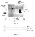
- Fig. 2is a simplified schematic diagram showing the stylus, sensors and excitation coil and describing the general principal of the preferred embodiments. Parts that are the same as in Fig. 1 are given the same reference numerals and are not described again except to the extent necessary for an understanding of the present figure.
- Triggering pulse 30is provided to excitation coil 26 that surrounds the sensor.
- Stylus 32comprises a resonant circuit 34, which is triggered by the excitation coil to oscillate at its resonant frequency. At the resonant frequency the circuit produces oscillations that continue after the end of the excitation pulse and steadily decay.
- the decaying oscillationsare sensed by the sensor arrangement which comprises a matrix or grid 12 of conductors. Accurate stylus positioning can be obtained, as will be explained below, from low amplitude vertical and horizontal signals that are picked up in the sensor arrangement and output to the front end units of Fig. 1 .
- the sensor arrangementin one preferred embodiment comprises a grid 12 of conductive lines.
- the gridpreferably comprises conductive polymers patterned on a polyester thermoplastic (PET) foil 40.
- PETpolyester thermoplastic
- the gridpreferably comprises two separate layers 42 and 44, electrically separated from each other by the PET layer 40.
- One of the layers 42contains a set of parallel conductors arranged in one direction.
- the other layer 44contains a set of parallel conductors orthogonal to those of the first layer.
- the parallel conductorsare straight antenna lines, connected at one end to an analog amplifier and at the other end to a common ground via a high value resistor.
- pairs of conductorsare shorted together to create conductive coil loops.
- one side of the loopis connected to the analog amplifier and the other side to the common ground.
- the two sides of the loopmay be connected to two inputs of a differential amplifier.
- the senoris patterned using transparent conductive materials so as to be mounted on top of a FPD.
- transparent conductive materialsare to enable the highest possible transparency of the sensor. It is preferable to minimize the visual difference between conductive and non-conductive sensor areas, as the user desires an unimpeded view of the screen.
- organic conductive materials on a PET foilis preferred as a solution which is flexible, easy to handle and minimizes the visual difference between conductive and non-conductive areas, as compared to other available solutions.
- ITOsemiconductor-based indium tin oxide
- the resistance of the conductive linesis relatively high and may exceed 100 KOhm for a line.
- higher resistance in the transparent conductorscorresponds to a higher transparency of the material. Therefore, it is desirable to work, in the present embodiments, with levels of resistance of the sensor grid that are as high as possible.
- patterning of the transparent sensoris implemented by printing conductive material in areas which are intended to conduct, that is to say the conductors are printed onto the film.
- An alternative embodimentcomprises forming a continuous layer of conductive material on the film and then removing the conductive materials from those areas which are not intended to conduct. Suitable methods for selectively removing the conductive material are well known in the art. Both of the above-mentioned ways are suitable as methods of manufacture, however, an advantage of the first mentioned method is the practically infinite resistance between the conductors. In the second, a finite leakage conductivity remains between the conductors as etching is not perfect. A disadvantage of both methods is a relatively noticeable visual difference between the conductive and non-conductive areas.
- a further embodimentcomprises a method of manufacturing the grid which minimizes the visual difference between conductive and non-conductive sensor areas.
- the entire areais coated with conductive material as before and then the non-conductive areas are passivated, that is to say they are treated to increase their resistance. As the same layers are present throughout the film, the visual difference between conductive and non-conductive areas is minimized.
- a film coated with the conductive polymeris subsequently further coated with a protective coating in those areas where conductivity is intended to be retained, that is the areas that are intended to conduct.
- the coatingcan be provided in many ways, for example screen printing, photolithography, etc.
- the film with the protective, or masking, layeris then rinsed with water in such a way as to avoid mechanical stress during rinsing. After rinsing it is immersed in a bath with a solution of hypochlorite at a defined chlorine concentration, PH, temperature and time, as will be clear to the person skilled in the art.
- the parametersare a key factor to achieve a result at the correct resistivity with the appropriate contrast between conductive and non-conductive lines, and the skilled person be able to carry out a certain amount of experimentation in order to optimize these parameters.
- the filmis then immediately passed through a series of distilled water baths to remove the chlorine. Finally the film is dried in an oven.
- the concentration of hypochorite usedwas 0.1%
- immersion timewas for 45 seconds
- the temperaturewas 25 degrees.
- Three distilled water bathswere used, and drying was carried out for 3 minutes at 50 degrees.
- the conductorsare straight lines having 1 mm width, equally spaced at 4 mm intervals.
- different sizes and spacingsmay be used. Large intervals between the lines may be selected in order to reduce the total number of conductors and therefore to reduce the complexity of the electronics and thus the price of the system and also increase reliability. Smaller intervals on the other hand may be selected to give higher resolution. Wider line width may be selected in order to reduce the resistance of a conductive line, again, at the cost of resolution.
- the resistance of parallel conductors in a certain foilis similar, and up to 5% tolerance is considered acceptable.
- other embodimentsmay be implemented with various differences between the line impedances, that is to say with larger tolerances, for example to reduce manufacturing costs. Such non-uniformity in principle leads to lower positioning accuracy.
- following manufacture of a given foiltesting is carried out over the conductors and a database is constructed to calibrate for any differences measured between the different conductors. The system thereby compensates automatically for the manufacturing tolerances.
- Such a databasecan be built either manually or automatically by the system.
- One way of automatic creation of such a databasecomprises providing the sensor with a common signal using the excitation coil, and then measuring the magnitude of the signals received by each of the conductors. The signals at each of the conductors are compared to a value that would be expected at zero tolerance and the differences are encoded in the database.
- the transparent sensoris constructed using three separate layers, which are implemented on three different foils.
- two layers 42 and 44are used for the sensor grid, one for the x axis conductors and one for the y axis conductors respectively, and the third layer, shown as 46 in the figure, is used to provide hard coating and anti-glare properties.
- Advantages of the three-layer embodimentinclude overall simplicity and, additionally, an ability to build the sensor using off-the-shelf components.
- a disadvantage of the approachis the relatively low overall transparency due to the presence of three separate foils in front of the display screen.
- a polyester PET foil 50is patterned on its lower size with horizontal conductors 52 and on its upper side with vertical conductors 54.
- the upper sideis covered and/or treated with suitable coatings to form hard coating layer 56, and the lower side is covered by a protective layer 58, helpful for avoiding integration or shipping damage.
- the gridis patterned onto Polyester PET foils.
- the grid, or part thereof, or any of the layersmay be patterned onto different materials such as glass or semiconductors or onto different types of plastic foils.
- the senoris surrounded by a non-transparent frame constructed from a PCB or any kind of flexible circuit.
- the framepreferably hosts the following components: front-end analog components, conductors for connecting the grid to the front-end, conductors for connecting the front-end to the digital processing section, and the excitation coil.
- the transparent conductorsare connected to the frame using vertically (Z) conductive glue.
- Zvertically conductive glue
- An example of such a vertically conductive glueis product no. 9703 manufactured by 3M Corporation.
- silver padsmay be printed on the edge of the transparent conductors. In an alternative embodiment, the silver pads may be avoided and the foil may be connected directly to the surrounding frame.
- the front-end componentsare mounted directly on the transparent foil.
- conductors to and from the front-endmay be implemented either by patterning applied to the transparent conductive material or by printing different materials, such as silver, onto the foil.
- the digital processing unitcomprises a separate board that is connected to the sensor via a cable.
- the size of the digital processing unitis reduced such that it may be mounted on the sensor frame or even on the edge of the foil.
- Fig. 5is a simplified block diagram showing the internal configuration of the front-end unit 16 of Fig. 1 according to a preferred embodiment of the present invention.
- the front end unit 16comprises a series of differential amplifiers 60.1..60.n.
- the differential amplifiersare connected in groups to switches 62.1..62.m.
- the switchespass on signals from one of the connected amplifiers to the next stage.
- the switchesare in turn connected to filter and amplifier circuits 64.1..64.m, and A/D converters 66.1..66.m.
- the A/D convertersare connected to an output buffer 68, which produces a final output signal for the digital processing unit.
- Each of the differential amplifiers 60.1..60.nis preferably connected via each of its differential inputs to a different one of the sensors of the grid.
- the two sensors that are connected to a single differential amplifierare preferably not adjacent sensors.
- the individual sensor signalsare thus converted into signals indicating the difference between two sensors.
- the difference signalis amplified and forward to switch 62.
- Each switchis connected between four amplifiers and selects one of the four available amplifier inputs to be further processed.
- the selected signalis amplified and filtered by the Filter & Amplifier 64, after which it is sampled by A/D converter 66.
- the digitized sampleis then forwarded to buffer 68 and sent on to the processing unit.
- the front endis implemented by a dedicated ASIC.
- the front-endmay be built from a combination of off-the-shelf components.
- Such an ASICcontains two A/D converters, two Filter & Amplifier units, two switches and eight differential amplifiers.
- Alternate embodimentsmay of course utilize different ASIC configurations, for example a different number of channels may be arranged in each IC or a different number of inputs may be provided to each of the switches.
- the switchmay be dispensed with altogether and the differential amplifiers may be connected directly to respective A/D converters.
- the switch 62is located before the Filter & Amplifier 64 thus saving on redundant components More particularly relocation of switch 62 in front of the filter and amplifier 64 reduces the total number of filters needed from 8 to 2. Such a configuration prevents fast switching between the inputs since the filter requires a relatively long setup time.
- the switch 62is placed after the Filter & amplifier 64 so that the filter and amplifier 64 is in proximity to the differential amplifier 60. In such a case it is possible to provide one filter 64 per differential amplifier 60.
- Such a configurationallows relatively fast switching between the inputs. In such a case, it is possible to add an A/D converter having a sampling rate which is several times higher than that required by the straightforward sampling procedure, so that more than one input can be sampled simultaneously.
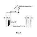
- Fig. 6is a simplified schematic diagram illustrating a scheme for connecting individual sensors of the grid to the differential amplifiers. Parts that are the same as in previous figures are given the same reference numerals and are not described again except to the extent necessary for an understanding of the present figure.
- two sensor lines 71 and 73that are close but not adjacent to one another, are selected. One of the two is then connected to the positive input of the differential amplifier 77 and the other is connected to the negative input of the same differential amplifier.
- the amplifieris thus able to generate an output signal which is an amplification of the difference between the two sensor line signals.
- An amplifier having a stylus on one of its two sensor lineswill produce a relatively high amplitude output.
- a major advantage of such a differential based schemeis its inherent noise reduction. If the two lines in the pair are placed relatively close to each other, than both lines probably sense the same parasitic noise and other effects, and the differential amplifier, which subtracts its inputs, thus eliminates any such noise. It is noted that the two input lines which are chosen for connection to the same amplifier are preferably not placed too close to each other, otherwise, a real input signal, such as the stylus signal, is likely to be sensed by both lines and removed by the differential amplifier. Therefore, in a preferred topology, the physical distance between lines connected to the same differential amplifier is slightly larger than the effective range of the stylus transmission. The digital processing unit is subsequently able to use the phase of the sampled signal to determine which of the two inputs of the amplifier have actually received the signal. If the phase is positive than the stylus is probably next to the line that is connected to the positive input of the amplifier and vice versa.
- regular amplifiersmay be used in place of differential amplifiers.
- the sensor linesare connected to the single inputs of the regular amplifiers.
- the sensor linesmay be patterned as loops, rather than straight lines arranged as a grid.
- one end of the loopmay be connected to a regular amplifier and the other end to a common ground.
- the two ends of a loopmay be connected to the positive and negative connections of a differential amplifier.
- the sensor linesare directly connected to the inputs of the differential amplifiers.
- the linesmay be connected via filters, preferably passive, to avoid saturation of the input amplifier due to large noise levels that may occur from time to time at the inputs.
- Fig. 7is a schematic diagram illustrating a variation of the scheme of Fig. 6 . Parts that are the same as in Fig. 6 are given the same reference numerals and are not described again except to the extent necessary for an understanding of the present figure.
- each of the inputs to differential amplifier 77is connected to two unrelated sensor lines. Thus both sensor lines 72 and 75 are connected to the same positive input of differential amplifier 77.
- Stylus 78is located next to sensor line number 2 and transmits a signal that can be picked up by line number 2 and its neighbors 71 and 73.
- the digital unitreceives a signal from differential amplifier 77, but initially does not know whether the signal source is line 72 or line 75.
- the digital unitis able to deduce the correct source of the signal.
- neighboring sensorsare connected to different amplifiers. Furthermore the neighbors of any two sensors connected to the same input should not be connected to corresponding inputs.
- the present embodimentsare especially applicable to mobile devices, generally battery powered. It is thus helpful to reduce energy consumption to a minimum.
- the front-end componentscontain a shutdown input command, which switches off various energy consuming chip activities.
- the digital processing unitmay then activate the shut down command as soon as the front-end is not required. Such an action may be activated periodically at a relatively high rate.
- FIG. 8is a simplified block diagram of the internal structure of a preferred embodiment of the digital processing unit 20 of Fig. 1 .
- a front-end interface 80receives serial inputs of sampled signals from the various front-end units 16 and arranges the inputs into a parallel representation.
- the parallel representationis transferred to DSP 82, which reads the sampled data, processes the data and determines or calculates the position of the physical objects such as the stylus. The calculated position is then sent to the host computer via link, preferably a serial link 84.
- Code for operating the DSP 84is preferably stored in Flash memory 86 and sampled data is stored in RAM 88. Excitation pulses for sending to the excitation coil are produced by the DSP 84, and then transformed into analog signals and amplified by unit 90 for output.
- the digital unitis implemented by a dedicated ASIC, which is preferably mounted on the sensor frame or foil edge.
- the digital unitmay be constructed from off-the-shelf components.
- a DSP coreprovides the above-described digital unit.
- Such a DSP coreis tailored for signal processing, enables high update rate and is capable of handling more than one object simultaneously.
- a cheaper micro-controllermay be selected for doing digital unit processing in place of a DSP.
- the DSP operating codeis stored in a Flash memory. Flash memory is easy to update and thus future improvements are simple to incorporate. However, if an update capability can be dispensed with, then cheaper ROM memory can be selected for storing the code.
- the DSPinterfaces a host computer via serial link 84.
- other types of interfacessuch as USB
- the USB interfaceis the preferred selection for an accessory type application, that is for an enhancement to an existing screen, since a USB is capable of providing the position detection arrangement of the present embodiments with a power supply.
- the USBis therefore a natural choice of connection type. If a USB interface is implemented, a USB interface component may be added to the digital unit 20 for handling communication with the host.
- the preferred embodimentsutilize a passive stylus, that is a stylus with no internal power source and no wired connection.
- external excitation coil 26which surrounds the sensor and thereby energizes the stylus resonance circuit.
- the receiving coilIn the passive stylus, energy from the external excitation coil induces currents in a receiving coil within the stylus.
- the receiving coilpreferably comprises a ferrite core.
- additional embodimentsmay utilize different types of receiving coils, such as air core or those having other types of cores.
- the receiving coilis preferably part of a resonant circuit within the stylus.
- COG capacitorsare selected to be included in the resonant circuit of the stylus.
- the advantages of such capacitorsare a low sensitivity to changes in temperature and good energy efficiency, the latter being important for a high Q factor and the former being important for a stable resonance frequency.
- other types of capacitormay be used.
- Stylus 100comprises a resonant circuit 102, and a frame 104 which defines a tip 106.
- resonant circuit 102oscillates at its resonant frequency.
- One side of the resonant circuit 102is electrically connected to the stylus tip 106, which preferably comprises a conductive material.
- the other side of the resonant circuitis electrically connected to frame 104, which likewise comprises conductive material
- Fig. 9illustrates a preferred way of providing such proximity.
- An electric field 108synchronized to the resonant circuit oscillations, is formed in a gap 110 located between the tip 106 and the frame 104. The geometric dimensions of the gap and the consequent field are relatively small and the field source is substantially close to the stylus tip.
- a resonant circuit 120comprises a basic resonant section 122 and a variation section 124.
- the basic resonant sectioncomprises an inductor 126 and capacitor 128. and is excited to oscillate at a basic resonant frequency selected for the stylus.
- the stylusfurther comprises a touch switch 130 and a right click switch 132.
- the stylus tip 134includes a gap as discussed previously for formation of the electric field. Furthermore the tip is designed to sense when it is in contact with the screen.
- the screenWhen the screen is in contact it causes touch switch 130 to close, thereby adding to the basic resonant circuit an additional capacitance 136 in parallel to capacitance 128.
- the effective capacitythus becomes C1 + C2 and the resonant frequency is altered.
- the signal processing unit 20is thereby able to determine whether the stylus is actually in contact with the screen or not.
- the applicationmay for example interpret touch of the stylus on the screen as the equivalent of a left click on the mouse.
- User pressuremay be used to close Right Click switch 132, thereby to connect capacitor 138 in parallel with capacitor 128.
- the switchthus changes the effective capacity to be C1 + C3 and again changes the resonance frequency.
- the digital unitdetects the change in the frequency and the application interprets the right click accordingly. If both switches 130 and 132 are closed at the same time a fourth frequency is detected by the digital unit equivalent to the capacitance of C1 + C2 + C3.
- the systemmay interpret the fourth frequency as a simultaneous left and right click.
- the above embodimentmay require excitation at four different frequencies, which wastes energy. It also requires analysis of four separate frequencies in the reception algorithm, thereby consuming CPU resources and energy.
- the above methodfurther requires use of a mechanical touch switch, which is placed in the path of the resonance circuit and therefore is required to pass relatively high current.
- the stylus touch switchneeds to be sensitive and thus designed to be closed under very low pressure.
- mechanical switches with low actuating forcedo not guarantee a stable and reliable contact.
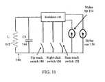
- FIG. 11is a simplified diagram illustrating an alternative circuit diagram for the stylus of Fig. 9 .
- a resonant circuitcomprises inductor 142 and capacitor 144 which are excited to oscillate at a predetermined resonant frequency.
- the resonance oscillationsare supplied to a modulator 146 which serves both as a source signal for modulation and as a power supply to the electronic components.
- the modulatoris fed by three inputs; a Tip touch switch 148 which indicates whether the tip of the stylus is touching a surface, a Right click switch 150 which indicates whether the user is pressing the right click button and a rear touch switch 152 which indicates whether the rear of the stylus is touching a surface.
- the normal state of any of the switchesmay be either closed or open.
- the tip touch switch 148may be closed when not in touch and open when in touch and vice versa.
- a normally closed stateis preferred to avoid bouncing whilst moving when in contact with the surface.
- One of the modulated signalsis provided to front tip 154 of the stylus, so that the position thereof may be determined during activities such as writing and pointing.
- the other signalis provided to the stylus rear 156, so that the stylus position can be detected for activities such as erasing, for which the stylus rear might be used.
- the modulator 146is capable of switching an output off, for example it may switch the rear signal off altogether when the rear switch does not indicate touch.
- the stylus statethat is any of hovering, left click, right click etc may be indicated by modulations introduced by modulator 146.
- the modulatormay introduce a variable time delay between the end of the excitation pulse and the beginning of the stylus signal.
- An exemplary modulation schemeis as follows: no delay for left click, that is stylus touching the surface, a delay of one oscillation when not touching, that is hovering, a delay of two oscillations for right click and a delay of three oscillations for erasing.
- modulation typesare used in place of delays to indicate the stylus state.
- Suitable modulation typesinclude phase shift (PSK), amplitude modulation (ASK), frequency shift (FSK), and others.
- the modulatorcan block transmission for a pre-defined amount of time, not during the course of the mode itself but when switching between modes.
- An example of such a techniqueis stopping tip transmission for one excitation cycle when switching from hovering to touch (left click down), stopping for two cycles when switching from touch to hovering (left click up), and so forth.
- the above embodimentsthus provide a stylus which is able to indicate its mode and yet only requires excitation and detection of a single frequency, thus saving energy and other resources.
- different gap geometriesmay be used for the tip and the rear of the stylus.
- the electric field at the tipmay be geometrically smaller and therefore sensed by fewer sensor lines than the rear field which is more spread out.
- the digital processing unitmay detect such a difference in field size and be able to determine which side of the stylus is touching the surface.
- Fig. 12is a simplified graphical illustration of waveform against time to describe the basic duty cycle of a preferred embodiment of the present invention.
- the cycleis divided into time periods t 0 ...t 4 which need not be of equal duration.
- the cyclebegins with the issuance of an excitation pulse 260 that lasts from t 0 to t 1 .
- the excitation pulseis produced by the digital unit 20, as described above, and transmitted by the excitation coil 26 surrounding the sensor.
- the pulsedrives relatively high signals on the sensor lines, which could cause saturation and other effects such as undesirable filter oscillations in the detection electronics. In order to avoid such ill effects the various detection channels at the front-end are blanked for the duration of the pulse.
- a blanking period 162is set, which preferably begins at to and ends at the beginning of t 2 .
- the systemthen waits for a predetermined period that allows the front-end filters to enter a ready state.
- This second wait, 164is known as the setup period, and upon completion thereof the detection electronics at the front end units sample the input signals during a sampling period 166 and convert the signals to digital representation as described above.
- all of the sensor input linesare sampled simultaneously during a single duty cycle.
- alternative embodimentsmay lack the resources to carry out such comprehensive sampling in a single cycle.
- the systemmay repeat the sampling cycle, two or more times, thus sampling a portion of the inputs for each cycle.
- the sampling rateis steady and is at least twice as fast as the highest sampled frequency, the Nyquist rate.
- additional implementationsmay change the sampling frequency in response to specific applications or in response to a specific situation.
- the digital unithas functionality for dynamically changing the sampling period.
- a longer sampling periodresults in a better signal to noise ratio (SNR) and greater ability to distinguish between neighboring frequencies.
- SNRsignal to noise ratio
- a shorter sampling periodsaves energy, saves computation and enables a faster update rate.
- Dynamic changing of the sampling periodcan be used to optimize between energy consumption and update rate as per the requirements of specific applications or specific situations. Alternatively, a constant sampling period can be provided.
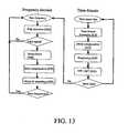
- Fig. 13is a simplified flow chart illustrating the procedure for processing the sensed data in order to determine a current position, according to a preferred embodiment of the present invention.
- the digital unitstarts processing the data in order to determine the physical object's position. Detection is performed in two basic phases; the first is a loop over each one of the sampled sensor lines, performing time-domain algorithms, and the second is a loop over frequency indexes, performing frequency domain algorithms.
- time domain activitiesbegin with averaging S10, in which samples from different cycles are averaged to improve SNR.
- the algorithmcompensates for the exponential decay of the oscillations.
- stage S30After which the sampled data is transformed into the frequency domain using either FFT or DFT in a stage S40. Time domain activity is repeated for all of the sensor lines.
- frequency domain activitiesstart with peak detection S50, in which the algorithm finds a location at which the signal at a given frequency is maximal, the frequency being selected to correspond to a given stylus in a given state. Then, in a stage S60, if a valid peak is detected, the algorithm interpolates the relevant signals to determine an accurate position. As will be recalled, a given signal is detected over a number of nearby sensors, and a position can be determined by interpolation to a greater accuracy than the granularity of the sensors. Issues of resolution, averaging and interpolation are discussed in greater detail below. In stage S70, fixed errors, if any, may be corrected, for example to compensate for steady electrical interference. Finally, in a stage S80, a determined position may be smoothed on the basis of positions from previous cycles.
- averagingis dynamically managed by the digital unit to optimize stability vs. update rate in accordance with requirements of specific applications or specific situations. In other embodiments, averaging may be avoided or may be carried out in a static manner.
- averagingmay either be carried out in the time domain, by averaging the samples themselves, or in the frequency domain, by averaging frequency coefficients. Both possibilities have the same mathematical affect in terms of masking noise and thus improving the SNR.
- time domain averagingis generally computationally more efficient since transforms need only be done once, however time domain averaging is wasteful of memory.
- averagingmay be carried out in the frequency domain.
- the signal emitted by the stylusis sampled during exponential decay of the resonance circuit oscillations.
- Transforming a decaying signal from the time to the frequency domaincan result in undesirable side lobes, which interfere with resolution. It is desirable to enable as good as possible distinction between close frequencies and to prevent false detection of frequencies not actually in use. Therefore, in a preferred embodiment, the system compensates for decay by multiplying the signal with the opposite exponential function.
- the resonance circuit Q factordrives the exponential coefficient of the decaying function.
- the Q factormay differ slightly from one physical object to another.
- the exponential compensation coefficientis a static value standing for the average Q factor.
- other embodimentsmay utilize a dynamic compensation coefficient that is specifically tuned, either manually or automatically, for each relevant object.
- the input samplesare multiplied by Hamming window coefficients prior to FFT / DFT transforming.
- the input samplesare multiplied by Hamming window coefficients prior to FFT / DFT transforming.
- undesired frequency side lobesare eliminated and false detections are avoided.
- different embodimentsuse different types of windows, such as Hanning, triangular or the like, or even use a simple square window with no additional modifications.
- the input samplesare transformed from the time to the frequency domain using either the DFT (Discrete Fourier Transform or FFT (Fast Fourier Transform).
- DFTDiscrete Fourier Transform
- FFTFast Fourier Transform
- the digital unitdynamically selects between FFT and DFT in accordance with the number of frequencies currently in use.
- Other possibilitiesare to preselect one or the other of the transforms based on the likely number of frequencies to be used in a given application.
- an applicationin which only a single stylus is ever likely to be used may initially be set to DFT.
- a chess gamein which each playing piece has a different frequency may be set to FFT, and a general purpose application may switch between the two transforms as the number of frequencies being used changes.
- Yet further embodimentsmay use other transformation from time to frequency domain.
- the magnitude or energy at the given frequencymay be used for calculating the object location after the transformation into the frequency domain.
- the phase of the input signalmay also be known, it may be possible to use the component of the frequency magnitude in the pre-known phase.
- a peak detection phasefollows in which a first rough determination is made of a location where the signal in is maximal.
- the algorithmlooks for the maximal magnitude in the X axis and simultaneously looks for the maximal magnitude in the Y-axis. If both the X and Y maximal magnitudes are determined to exceed a preset threshold, than a physical object is likely to be located about the intersection of the two maximal coordinates.
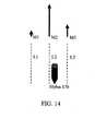
- Fig. 14is a simplified diagram illustrating a stylus 170 located in proximity to three sensing lines L1, L2 and L3 and generating signals M1, M2 and M3 respectively.
- Stylus 170is not accurately located opposite any of the sensing lines but rather is at an intermediate position between two of them.
- an interpolation phasefollows to increase the accuracy of the determined location. That is to say, the object of the interpolation phase is to determine an accurate location of the physical object beyond the granularity of the sensing devices.
- interpolationis performed on detection data measured from two input lines, the line having the maximal magnitude for the given axis as determined in the previous stage, and the neighboring line having the next highest magnitude.
- stylus 170is placed next to lines L1, L2 and L3.
- the linessense signals of magnitudes M1, M2 and M3 respectively.
- the stylusis located between lines L2 and L3, at a position closer to L2.
- L2 (M2)senses the highest signal magnitude
- L3 (M3)senses a lower signal magnitude
- L1 (M1)senses the lowest magnitude.
- the algorithmdetects L2 as the line having the maximal magnitude (M2).
- Different embodimentsmay use different interpolation functions, different interpolation algorithms or larger number of lines in the interpolation process.
- interpolation based on the three lines having the highest signalsmay be expected to provide improved location accuracy for relatively little increase in processing cost.
- the error compensation stage, S70 in Fig. 13corrects systematic errors that are caused by static electric interference, such as that imposed by the FPD structure and topology.
- static electric interferencesuch as that imposed by the FPD structure and topology.
- a front mounted sensoris not sensitive to this type of interference and therefore no error compensation is used.
- error compensation of this kindis useful.
- One way of implementing such an error correction processis to use a customized look-up table.
- the look up tablemay be operated on the host computer or be configured into the digital processing unit, and is typically in the form of a two-dimensional matrix.
- the matrix cellsrepresents sensor coordinates and the cells content is a two-dimensional error value for the relevant position.
- Such a matrixmay automatically be built as a final stage of the manufacture process by a robot arm system that moves a stylus through a series of pre-defined known locations and stores data relating to the difference between the known and the actually detected positions.
- the systemmay either select the error value stored in the matrix cell closest to the reported position, or may interpolate a detected value by a number of matrix cells around the reported position according to the error value given.
- the matrixmay be combined with the sensor line tolerance compensation database referred to above if present.
- Stage 80 of the flow chart of Fig. 13relates to smoothing.
- the object of the smoothing stageis to smooth stylus movement using the history of the previous stylus positions.
- the smoothingfilters out temporary and static fluctuations that are not a reasonable human movement, in order to display a smoother image on the graphical display.
- the smoothing phaseis implemented at the host computer. Implementation may be as a dedicated package in the system driver or as part of general support provided within the operating system. In another embodiment, smoothing is carried out at the digital unit 20.
- smoothingcomprises filtering undesired frequencies from the movement pattern. This may, for example, be achieved by transforming the vector obtained of successive stylus positions into the frequency domain, setting undesired frequency coefficients to zero, and switching back to the time domain for display purposes.
- Other embodiments of the present inventionmay use other types of filters, such as filters that fit a best curve, and the like.
- smoothing filters that use both history and future positionsnormally perform better than those that use history alone.
- using both historical and future positionscan make it difficult to produce real time results, due to the need to make an assessment of likely future positions.
- the above disadvantageis significant while writing or painting on a display such as an FPD, wherein the user expects the drawing to match the tip of the stylus closely.
- One solutionis to use a combination of two filters; the first being a reactive filter, or even no filter at all, that has a tiny delay and which is used to provide stylus movement tracking on the screen in real time.
- the secondis a slower filter that uses future knowledge and back-corrects the already displayed curve, so that glitches disappear before they are able to do any harm.
- the excitation pulseis a dominant energy consumer. It is desirable to minimize energy consumption overall, especially as many likely applications for the present embodiments are on battery-powered portable devices of one kind or another. It is therefore preferable to minimize the pulse energy consumption.
- the excitation pulsecomprises one or more sine waves.
- other types of pulsesuch as impulse, square wave and like pulses may be used.
- the digital unitdynamically controls the excitation signal pattern.
- the systemis aware of the objects and corresponding frequencies currently taking part in a given session, and produces excitation waves accordingly.
- System awareness of participating objectsmay be provided as pre-knowledge from the application or as a dynamic analysis of the current inputs.
- the systemobtains the frequencies of the participating devices from the application, or interrogates the participating devices or analyzes its inputs to determine the frequencies present.
- the systemthen restricts the excitation signal pattern to that optimal for those frequencies.
- Other embodimentsmay use a static pulse pattern that ensures the excitation of all relevant frequencies.
- a longer excitation pulseresults in lower energy consumption.
- a long pulsemay limit the overall update rate.
- preferred embodimentsoptimize energy consumption and update rate to the requirements of specific applications or specific situations, either by preselecting an optimal excitation pulse length for the application or by dynamically changing the pulse length during operation.
Landscapes
- Engineering & Computer Science (AREA)
- General Engineering & Computer Science (AREA)
- Theoretical Computer Science (AREA)
- Physics & Mathematics (AREA)
- Human Computer Interaction (AREA)
- General Physics & Mathematics (AREA)
- Electromagnetism (AREA)
- Position Input By Displaying (AREA)
- Liquid Crystal Substances (AREA)
- Mechanical Pencils And Projecting And Retracting Systems Therefor, And Multi-System Writing Instruments (AREA)
Abstract
Description
- The present invention relates to a transparent digitizer and, more particularly, but not exclusively to a transparent digitizer with a cordless stylus or like input device.
US Patent Application No. 09/628,334 - Touch technologies are commonly used as input devices for a variety of products. The usage of touch devices of various kinds is growing sharply due to the emergence of new mobile devices, such as Web-Pads, Web Tablets, PDAs, Tablet PCs and wireless Flat Screen Displays. These new devices are usually not connected to standard keyboards, mice or like input devices, which are deemed to limit their mobility. Instead there is a tendency to use touch input technologies of one kind or another.
- Some of the new mobile devices, such as the Tablet PC, are powerful computer tools. Devices such as the Tablet PC use a stylus based input device, and use of the Tablet PC as a computing tool is dependent on the abilities of the stylus input device. The input devices have the accuracy to support hand writing recognition and full mouse emulation, for example hovering, right click, etc. Manufacturers and designers of these new mobile devices have determined that the stylus input system can be based on various electromagnetic technologies, which can satisfy the very high performance requirements of the computer tools in terms of resolution, fast update rate, and mouse functionality. However, in general, the stylus systems in use are tablet based, that is the stylus is moved over a tablet which in itself is not a screen. There have been attempts in the past to combine non-transparent electro magnetic digitizer technology with a transparent Flat Screen Display.
US patent number 6,005,555 to Wacom describes a digitizer comprising two layers of orthogonal conductive loops. One set of conductive loops is used for transmitting an excitation signal while the orthogonal set of loops is used for receiving oscillations. However, a requirement of the Wacom system is high conductivity within the loops. As such, Wacom's method has to use loops made of standard metallic conductors and cannot be used with transparent conductive foils, since the resistance of a conductive transparent line is very high. Using high resistance conductive loops to energize the stylus requires a particularly high voltage input, in excess of 1 KV, which makes this solution impractical. Without the use of transparent conductive material, however, the solution of Wacom merely succeeds in making the display difficult to view. - One way of overcoming the difficulty of viewing the display is to place the non-transparent sensor of Wacom behind the display. Thus the sensor may be located between the FPD back-light and the electronic board of the display device. As such, integration of a non-transparent sensor into a FPD device is a very complicated and expensive process. Such mounting typically requires shielding of noisy components within the device and sometimes requires the manufacturing of a special slot in the FPD structure, in which the sensor is mounted.
- A non-transparent sensor, if located behind the display, is inevitably relatively far away from the tip of the stylus whose position it is trying to determine. Due to the relatively long distance from the sensor, non-transparent sensors suffer from parallax, leading to inaccurate positioning of the stylus. Positioning is especially inaccurate, that is parallax effects are especially large, when the stylus is held at an angle to the display. Yet, applications such as handwriting detection demand that the system is tolerant to the stylus being held at an angle to the screen.
- Furthermore, again due to the relatively long distance from the sensor, back-mounted sensors suffer from inaccurate positioning of the stylus when the stylus is held close to the edge of the sensor.
- In summary, due to the relatively long distance from the sensor, and furthermore due to the number of electronically active components likely to be located between the sensor and the stylus, back-mounted sensors may not achieve reliable positioning resolution.
- There have been attempts in the past to overcome the disadvantages of a back mounted sensor by implementation of a sensor based on a transparent foil. As the sensor is transparent it can be mounted on the front of the screen. However, such a detector relies on transparent conductors, which have a high resistivity compared to opaque conductors.
US Patent No. 5,381,160 to Kurta describes a foil comprising two transparent layers of orthogonal conductors. Kurta's disclosure describes a solution to a problem that arises in light of the above-mentioned high resistivity of the conductors, namely how to excite the physical object whose position is to be determined despite the high resistivity. The solution is simply to use an active stylus, internally powered by its own battery. The stylus therefore does not require external excitation. However, an active, battery powered stylus is generally not regarded as a satisfactory solution for a number of reasons. For example, an active stylus requires continuous maintenance and may even stop working and thereby render the entire computer device inoperable. Also the active stylus requires recharging, and is more expensive than a passive device. Therefore, an active stylus is currently unacceptable for the mobile consumer market. - The above-mentioned application to Gamalong discloses a sensor, for a passive stylus, based on transparent foils where a separate excitation coil is located about the screen. The stylus or other object whose position is to be detected comprises a resonant circuit. The resonant circuit is excited by the excitation coil to generate an electric field, and the electric field is detected by the relatively highly resistive detection conductors on the transparent foils. A problem however, is that detection, which is based on electric fields, is carried out on the surface of an electronic display screen, and the screen surface is a relatively high noise environment in terms of electromagnetic activity. The high noise environment necessarily reduces the resolution level of the digitizer.
US Patent No, 5,854,881 to Sharp Kabushiki Kaisha describes an LCD panel having electrodes, a magnetic field generator which outputs an AC magnetic field from a tip end of its electrode, a differential amplifier, switching circuits which sequentially select electrodes of the LCD panel and connect the electrodes to the differential amplifier, and a coordinate detection circuit which detects the coordinates of a position in which the magnetic field generator is located based on a timing at which the electrodes are selected and an output of the differential amplifier, Multiple switching between different amplifier connections is often required to determine a location of the magnetic field generator from said differential signals.- There is thus a widely recognized need for, and it would be highly advantageous to have, a stylus based transparent digitizer devoid of the above limitations.
- It is a general object of the present invention to enable effective usage of a transparent sensor together with a passive stylus in a high noise environment according to the appended claims.
- The invention is herein described, by way of example only, with reference to the accompanying drawings. With specific reference now to the drawings in detail, it is stressed that the particulars shown are by way of example and for purposes of illustrative discussion of the preferred embodiments of the present invention only, and are presented in the cause of providing what is believed to be the most useful and readily understood description of the principles and conceptual aspects of the invention. In this regard, no attempt is made to show structural details of the invention in more detail than is necessary for a fundamental understanding of the invention, the description taken with the drawings making apparent to those skilled in the art how the several forms of the invention may be embodied in practice.
- In the drawings:
FIG. 1 is a simplified block diagram of a digitizer according to a first preferred embodiment of the present invention;FIG. 2 is a simplified schematic diagram showing the stylus, sensors and excitation coil ofFig. 1 , and describing a general principal of the preferred embodiments;FIG. 3 is a simplified diagram illustrating a preferred embodiment of a sensor for use in the digitizer ofFig. 1 ;FIG. 4 is a one-foil configuration of a sensor for use with the embodiment ofFig. 1 , in which a Polyester PET foil is patterned on its lower size with horizontal conductors and on its upper side with vertical conductors;FIG. 5 is a simplified schematic diagram illustrating the internal configuration of the front-end unit ofFig. 1 according to a preferred embodiment of the present invention;FIG. 6 is a simplified schematic diagram illustrating a scheme for connecting individual sensors of the grid to the differential amplifiers;FIG. 7 is a schematic diagram illustrating a variation of the scheme ofFig. 6 ;FIG. 8 is a simplified block diagram of the internal structure of a preferred embodiment of thedigital processing unit 20 ofFig. 1 ;FIG. 9 is a simplified diagram of the internal construction of a stylus according to a preferred embodiment of the present invention;FIG. 10 is a simplified circuit diagram for the stylus ofFig. 9 ;FIG. 11 is a simplified diagram illustrating an alternative circuit diagram for the stylus ofFig. 9 ;FIG. 12 is a simplified graphical illustration of waveform against time to describe the basic duty cycle of a preferred embodiment of the present invention;FIG. 13 is a simplified flow chart illustrating the procedure for processing the sensed data in order to determine a current position, according to a preferred embodiment of the present invention; andFIG. 14 is a simplified diagram illustrating a stylus located in proximity to three sensing lines and generating signals in the sensing lines respectively.- The present embodiments disclose a method and apparatus for locating and identifying physical objects, such as a stylus or game tokens, on top of a Flat Panel Display. The location of the physical objects is sensed by an electro magnetic transparent digitizer, which is preferable mounted on top of the display. The physical objects are preferably passive elements, that is they do not include any kind of internal power source. The passive elements are energized by a non-transparent excitation coil, which is placed substantially about the transparent sensor. The transparent sensor comprises a sensing grid or an arrangement of sensing loops, whose outputs are connected to sensing amplifiers. In one preferred embodiment the sensing amplifiers are differential amplifiers and in one preferred embodiment each sensing amplifier is connected to at least two non-adjacent outputs from the grid.
- A further preferred embodiment comprises an arrangement of the passive stylus in which a projection of wires into the tip is made in order to provide a sharp and therefore more easily detectable electric field. The concentration of the field at the tip allows the field to be distinguished more easily from noise and thereby improves the resolution of the digitizer.
- The principles and operation of a transparent digitizer according to the present invention may be better understood with reference to the drawings and accompanying descriptions.
- Before explaining at least one embodiment of the invention in detail, it is to be understood that the invention is not limited in its application to the details of construction and the arrangement of the components set forth in the following description or illustrated in the drawings. The invention is capable of other embodiments or of being practiced or carried out in various ways. Also, it is to be understood that the phraseology and terminology employed herein is for the purpose of description and should not be regarded as limiting.
- A preferred use for the present embodiments is a transparent digitizer for a mobile computing device that uses a flat panel display (FPD) screen. The digitizer of the present embodiments detects the position of one or more styluses at a very high resolution and update rate. The stylus is applicable to any standard stylus use, including pointing, painting, writing, including handwriting recognition applications, and deleting, and may also be applied to any other activity that can be stylus based. The stylus, together with the digitizer, may for example support full mouse emulation. In a typical mouse emulation application, as long as the stylus hovers above the FPD, a mouse cursor follows the stylus position. Touching the screen is equivalent to the left click of a mouse and a switch located on the stylus emulates right click operation. As well as full, or partial, mouse emulation, different embodiments may support various additional features such as an Eraser, change of color, etc.
- In a preferred embodiment, the digitizer communicates with the host computer using a serial link, such as RS232. However, in different embodiments the digitizer may communicate via USB or any other type of communication. In some embodiments the digitizer may even communicate with the host using a wireless link such as based on Infrared, Ultrasonics or RF.
- In a preferred embodiment, the mobile device is an independent computer system having its own CPU. In different embodiments the mobile device may only be a part of system, for example it may be a wireless mobile screen for a Personal Computer. In other embodiments the digitizer is used with a standard desktop computer. A digitizer built into the screen may be particularly useful for computers in hazardous environments such as on a factory floor.
- In a preferred embodiment, the digitizer is integrated into the host device on top of the FPD screen. In additional embodiments the transparent digitizer may be provided as an accessory to be placed on top of an existing screen. Such a configuration can be very useful for laptop computers already in the market in very large numbers. An embodiment of the present invention may comprise an accessory to transform an existing laptop into a powerful device that supports hand writing, painting or any other operation enabled by the transparent digitizer.
- In a preferred embodiment, the digitizer supports a single stylus. However, different embodiments may be used for supporting more than one stylus operating simultaneously on the same screen. Such a configuration is very useful for entertainment applications which require more than one user to paint or write to the same paper-like screen, perhaps even simultaneously. The present embodiments may further be used in applications which require more than one object to be detected, for example games with a plurality of playing pieces. In such a game, the display may for example show a game board for a particular game. The physical objects are shaped as the tokens, gaming pieces, toys, simulation figures and the like as required by the game being displayed. An arrangement supporting gaming over a transparent screen is described in
US Patent Application 09/628,334 to Gamalong US Provisional Patent Application 60-333,770 to N-trig - In a preferred embodiment, the digitizer is implemented using a set of transparent foils which are placed on the transparent screen, as will be explained in greater detail below. However, certain embodiments may be implemented using other kinds of transparent, or even a non-transparent, sensor. One example of an embodiment which does not use a transparent screen is a Write Pad device, which is a thin digitizer that is placed below normal paper. The user writes on the paper using a stylus that combines real ink with electro-magnetic functionality. The user writes on the normal paper and the input is simultaneously transferred to a host computer to store or analyze the data. It will be appreciated that, given the thinness of paper, the parallax effects of the screen thickness do not apply. Furthermore, the noise effects due to intervening electronic components also do not apply.
- An additional example of how the present invention can be applied to a non-transparent sensor is an electronic entertainment board. The digitizer, in this example, is mounted below a graphic image of a board, and detects the position and identity of gaming figures that are placed on top of the board. The graphic image in this case is static, but it could be manually replaced from time to time, such as when switching to a different game.
- In one preferred embodiment of the present invention, a non-transparent sensor may be integrated into the back of a FPD. One example of such an embodiment is an electronic entertainment device having a FPD display. The device may be used for games, during the course of which the digitizer detects the position and identity of gaming figures. It could also be used for painting and / or writing, and the digitizer may be required to detect one or more styluses. In many cases, a configuration of a non-transparent sensor with an FPD can be sufficient when high performance is not critical for the application.
- Reference is now made to
Fig. 1 , which is a simplified block diagram of a first preferred embodiment of the present invention. A digitizer arrangement is applied to a displayscreen host arrangement 10. The digitizer arrangement comprises a grid-basedsensor 12, which is preferably transparent, and which is located on top of anFPD 14. Analog front-end ASICs 16 are preferably mounted on the frame of the sensor. The ASICS are preferably connected to outputs of the various conductors in the grid as will be explained in greater detail hereinbelow. Each front-end receives very low amplitude signals as output by the sensor conductors. It will be recalled that the sensor conductors, being transparent, have relatively high resistivity, limiting the amplitude of output signals. TheASIC 16 comprises circuitry to amplify the signal, identify and filter out irrelevant frequencies, sample the output into a digital representation and forward the sampled data to adata bus 18 for further digital processing atdigital processing unit 20.Digital processing unit 20 is responsible for running various digital processing algorithms, as will be discussed in greater detail hereinbelow. The outcome of the digital processing performed byunit 20 is preferably the position of one or more physical objects, typically the position of the stylus, and the outcome, once determined, is forwarded to host 22 viainterface 24 for processing by the operating system or any currant application. In a preferred embodiment the digital unit communicates with the host via a simple serial interface. Additional interfaces, such as USB, are possible. - An additional task of the
digital processing unit 20 is to produce and manage a triggering pulse to be provided toexcitation coil 26 that surrounds the sensor arrangement and the display screen. The excitation coil provides a trigger pulse that excites passive circuitry in the stylus to produce a response from the stylus that can subsequently be detected. - Reference is now made to
Fig. 2 , which is a simplified schematic diagram showing the stylus, sensors and excitation coil and describing the general principal of the preferred embodiments. Parts that are the same as inFig. 1 are given the same reference numerals and are not described again except to the extent necessary for an understanding of the present figure. Triggeringpulse 30 is provided toexcitation coil 26 that surrounds the sensor.Stylus 32 comprises aresonant circuit 34, which is triggered by the excitation coil to oscillate at its resonant frequency. At the resonant frequency the circuit produces oscillations that continue after the end of the excitation pulse and steadily decay. The decaying oscillations are sensed by the sensor arrangement which comprises a matrix orgrid 12 of conductors. Accurate stylus positioning can be obtained, as will be explained below, from low amplitude vertical and horizontal signals that are picked up in the sensor arrangement and output to the front end units ofFig. 1 . - Reference is now made to
Fig. 3 , which is a simplified diagram illustrating a preferred embodiment of the sensor arrangement. As explained above, the sensor arrangement in one preferred embodiment comprises agrid 12 of conductive lines. The grid preferably comprises conductive polymers patterned on a polyester thermoplastic (PET) foil 40. The grid preferably comprises twoseparate layers layers 42 contains a set of parallel conductors arranged in one direction. Theother layer 44 contains a set of parallel conductors orthogonal to those of the first layer. - In a preferred embodiment, the parallel conductors are straight antenna lines, connected at one end to an analog amplifier and at the other end to a common ground via a high value resistor. In an alternative embodiment, pairs of conductors are shorted together to create conductive coil loops. In such an embodiment, one side of the loop is connected to the analog amplifier and the other side to the common ground. Alternatively, in the case of loops, the two sides of the loop may be connected to two inputs of a differential amplifier.
- In a preferred embodiment, the sensor is patterned using transparent conductive materials so as to be mounted on top of a FPD. The use of such materials is to enable the highest possible transparency of the sensor. It is preferable to minimize the visual difference between conductive and non-conductive sensor areas, as the user desires an unimpeded view of the screen.
- The use of organic conductive materials on a PET foil is preferred as a solution which is flexible, easy to handle and minimizes the visual difference between conductive and non-conductive areas, as compared to other available solutions. However, for certain applications, different considerations may apply and thus implementations using other transparent conductive materials may be considered. An example of an alternative choice is semiconductor-based indium tin oxide (ITO).
- In a preferred embodiment, the resistance of the conductive lines is relatively high and may exceed 100 KOhm for a line. In general, higher resistance in the transparent conductors corresponds to a higher transparency of the material. Therefore, it is desirable to work, in the present embodiments, with levels of resistance of the sensor grid that are as high as possible.
- There are a number of possible methods of applying the conductors to the film. In a first preferred embodiment, patterning of the transparent sensor is implemented by printing conductive material in areas which are intended to conduct, that is to say the conductors are printed onto the film. An alternative embodiment comprises forming a continuous layer of conductive material on the film and then removing the conductive materials from those areas which are not intended to conduct. Suitable methods for selectively removing the conductive material are well known in the art. Both of the above-mentioned ways are suitable as methods of manufacture, however, an advantage of the first mentioned method is the practically infinite resistance between the conductors. In the second, a finite leakage conductivity remains between the conductors as etching is not perfect. A disadvantage of both methods is a relatively noticeable visual difference between the conductive and non-conductive areas.
- A further embodiment comprises a method of manufacturing the grid which minimizes the visual difference between conductive and non-conductive sensor areas. In the further embodiment, the entire area is coated with conductive material as before and then the non-conductive areas are passivated, that is to say they are treated to increase their resistance. As the same layers are present throughout the film, the visual difference between conductive and non-conductive areas is minimized.
- One disadvantage of using the above process, and selectively increasing resistance after forming the conductive layer, is that whilst high resistivity is produced, it is still far short of an insulator. The process thus results in relatively high parasitic inductance and leakage current between the patterned lines. Careful selection of parameters during the passivation process can minimize such effects.
- Considering the embodiment in which conductive polymer is coated and then passivated, a film coated with the conductive polymer is subsequently further coated with a protective coating in those areas where conductivity is intended to be retained, that is the areas that are intended to conduct. The coating can be provided in many ways, for example screen printing, photolithography, etc. The film with the protective, or masking, layer, is then rinsed with water in such a way as to avoid mechanical stress during rinsing. After rinsing it is immersed in a bath with a solution of hypochlorite at a defined chlorine concentration, PH, temperature and time, as will be clear to the person skilled in the art. The parameters are a key factor to achieve a result at the correct resistivity with the appropriate contrast between conductive and non-conductive lines, and the skilled person be able to carry out a certain amount of experimentation in order to optimize these parameters. After the hypochlorite bath the film is then immediately passed through a series of distilled water baths to remove the chlorine. Finally the film is dried in an oven.
- In an example, the concentration of hypochorite used was 0.1%, immersion time was for 45 seconds, and the temperature was 25 degrees. Three distilled water baths were used, and drying was carried out for 3 minutes at 50 degrees.
- In a preferred embodiment, the conductors are straight lines having 1 mm width, equally spaced at 4 mm intervals. Depending on the application however, different sizes and spacings may be used. Large intervals between the lines may be selected in order to reduce the total number of conductors and therefore to reduce the complexity of the electronics and thus the price of the system and also increase reliability. Smaller intervals on the other hand may be selected to give higher resolution. Wider line width may be selected in order to reduce the resistance of a conductive line, again, at the cost of resolution.
- The magnitude of a signal received by a specific line is dependent on the resistance of that line, and the position of the stylus is determined by the relative magnitude of the signals received by the whole grid. Therefore, in one embodiment, the resistance of parallel conductors in a certain foil is similar, and up to 5% tolerance is considered acceptable. However, other embodiments may be implemented with various differences between the line impedances, that is to say with larger tolerances, for example to reduce manufacturing costs. Such non-uniformity in principle leads to lower positioning accuracy. However, in one preferred embodiment, following manufacture of a given foil, testing is carried out over the conductors and a database is constructed to calibrate for any differences measured between the different conductors. The system thereby compensates automatically for the manufacturing tolerances. Such a database can be built either manually or automatically by the system. One way of automatic creation of such a database comprises providing the sensor with a common signal using the excitation coil, and then measuring the magnitude of the signals received by each of the conductors. The signals at each of the conductors are compared to a value that would be expected at zero tolerance and the differences are encoded in the database.
- Returning to the issue of construction of the sensing apparatus, and in one embodiment, the transparent sensor is constructed using three separate layers, which are implemented on three different foils. As shown in
Fig. 3 , twolayers - A further embodiment is now described in which the sensing arrangement is constructed using a single foil and thereby improving overall transparency. Reference is now made to
Fig. 4 which shows such a one-foil configuration. InFig. 4 , apolyester PET foil 50 is patterned on its lower size withhorizontal conductors 52 and on its upper side withvertical conductors 54. The upper side is covered and/or treated with suitable coatings to formhard coating layer 56, and the lower side is covered by aprotective layer 58, helpful for avoiding integration or shipping damage. - The skilled person will note that additional implementations are possible such as embodiments based on two foils.
- In a preferred embodiment, the grid is patterned onto Polyester PET foils. However, in different embodiments, the grid, or part thereof, or any of the layers, may be patterned onto different materials such as glass or semiconductors or onto different types of plastic foils.
- In a preferred embodiment, the sensor is surrounded by a non-transparent frame constructed from a PCB or any kind of flexible circuit. The frame preferably hosts the following components: front-end analog components, conductors for connecting the grid to the front-end, conductors for connecting the front-end to the digital processing section, and the excitation coil.
- In a preferred embodiment, the transparent conductors are connected to the frame using vertically (Z) conductive glue. An example of such a vertically conductive glue is product no. 9703 manufactured by 3M Corporation. In order to get a reliable connection to the frame, silver pads may be printed on the edge of the transparent conductors. In an alternative embodiment, the silver pads may be avoided and the foil may be connected directly to the surrounding frame.
- In another preferred embodiment, the front-end components are mounted directly on the transparent foil. In this case conductors to and from the front-end may be implemented either by patterning applied to the transparent conductive material or by printing different materials, such as silver, onto the foil.
- In one preferred embodiment, the digital processing unit comprises a separate board that is connected to the sensor via a cable. In an additional embodiment, the size of the digital processing unit is reduced such that it may be mounted on the sensor frame or even on the edge of the foil.
- Reference is now made to
Fig. 5 , which is a simplified block diagram showing the internal configuration of the front-end unit 16 ofFig. 1 according to a preferred embodiment of the present invention. Thefront end unit 16 comprises a series of differential amplifiers 60.1..60.n. The differential amplifiers are connected in groups to switches 62.1..62.m. The switches pass on signals from one of the connected amplifiers to the next stage. The switches are in turn connected to filter and amplifier circuits 64.1..64.m, and A/D converters 66.1..66.m. The A/D converters are connected to anoutput buffer 68, which produces a final output signal for the digital processing unit. - Each of the differential amplifiers 60.1..60.n is preferably connected via each of its differential inputs to a different one of the sensors of the grid. As will be explained below, the two sensors that are connected to a single differential amplifier are preferably not adjacent sensors. The individual sensor signals are thus converted into signals indicating the difference between two sensors. The difference signal is amplified and forward to switch 62. Each switch is connected between four amplifiers and selects one of the four available amplifier inputs to be further processed. The selected signal is amplified and filtered by the Filter & Amplifier 64, after which it is sampled by A/D converter 66. The digitized sample is then forwarded to buffer 68 and sent on to the processing unit.
- In a preferred embodiment, the front end is implemented by a dedicated ASIC. However, in different embodiments, the front-end may be built from a combination of off-the-shelf components.
- In the preferred embodiment illustrated, each front-end ASIC contains two identical channels, each handling four differential inputs, so that, in the reference numerals of the figures, n = 8 and m = 2. Such an ASIC contains two A/D converters, two Filter & Amplifier units, two switches and eight differential amplifiers. Alternate embodiments may of course utilize different ASIC configurations, for example a different number of channels may be arranged in each IC or a different number of inputs may be provided to each of the switches. In one embodiment the switch may be dispensed with altogether and the differential amplifiers may be connected directly to respective A/D converters. An advantage of such a configuration is that it is possible to sample all input lines at the same time, but at a cost of increased complexity. Full simultaneous sampling is useful for energy saving, since all inputs are sampled at each excitation pulse, thus requiring only a single excitation pulse per detection. A significant disadvantage of the above embodiment, where all inputs are sampled simultaneously, is its relatively higher price.
- In a preferred embodiment, the switch 62 is located before the Filter & Amplifier 64 thus saving on redundant components More particularly relocation of switch 62 in front of the filter and amplifier 64 reduces the total number of filters needed from 8 to 2. Such a configuration prevents fast switching between the inputs since the filter requires a relatively long setup time. However, in a different embodiment, the switch 62 is placed after the Filter & amplifier 64 so that the filter and amplifier 64 is in proximity to the differential amplifier 60. In such a case it is possible to provide one filter 64 per differential amplifier 60. Such a configuration allows relatively fast switching between the inputs. In such a case, it is possible to add an A/D converter having a sampling rate which is several times higher than that required by the straightforward sampling procedure, so that more than one input can be sampled simultaneously.
- Reference is now made to
Fig. 6 , which is a simplified schematic diagram illustrating a scheme for connecting individual sensors of the grid to the differential amplifiers. Parts that are the same as in previous figures are given the same reference numerals and are not described again except to the extent necessary for an understanding of the present figure. In the scheme, twosensor lines differential amplifier 77 and the other is connected to the negative input of the same differential amplifier. The amplifier is thus able to generate an output signal which is an amplification of the difference between the two sensor line signals. An amplifier having a stylus on one of its two sensor lines will produce a relatively high amplitude output. A major advantage of such a differential based scheme is its inherent noise reduction. If the two lines in the pair are placed relatively close to each other, than both lines probably sense the same parasitic noise and other effects, and the differential amplifier, which subtracts its inputs, thus eliminates any such noise. It is noted that the two input lines which are chosen for connection to the same amplifier are preferably not placed too close to each other, otherwise, a real input signal, such as the stylus signal, is likely to be sensed by both lines and removed by the differential amplifier. Therefore, in a preferred topology, the physical distance between lines connected to the same differential amplifier is slightly larger than the effective range of the stylus transmission. The digital processing unit is subsequently able to use the phase of the sampled signal to determine which of the two inputs of the amplifier have actually received the signal. If the phase is positive than the stylus is probably next to the line that is connected to the positive input of the amplifier and vice versa. - In an alternative embodiment, regular amplifiers may be used in place of differential amplifiers. In such a case the sensor lines are connected to the single inputs of the regular amplifiers.
- In a further alternative embodiment the sensor lines may be patterned as loops, rather than straight lines arranged as a grid. In such a case one end of the loop may be connected to a regular amplifier and the other end to a common ground. Alternatively, the two ends of a loop may be connected to the positive and negative connections of a differential amplifier.
- In a preferred embodiment, the sensor lines are directly connected to the inputs of the differential amplifiers. However, as an alternative, the lines may be connected via filters, preferably passive, to avoid saturation of the input amplifier due to large noise levels that may occur from time to time at the inputs.
- A further embodiment is now explained with respect to
Fig. 7 , which is a schematic diagram illustrating a variation of the scheme ofFig. 6 . Parts that are the same as inFig. 6 are given the same reference numerals and are not described again except to the extent necessary for an understanding of the present figure. In the variation ofFig. 7 , each of the inputs todifferential amplifier 77 is connected to two unrelated sensor lines. Thus bothsensor lines differential amplifier 77. Stylus 78 is located next to sensor line number 2 and transmits a signal that can be picked up by line number 2 and itsneighbors differential amplifier 77, but initially does not know whether the signal source isline 72 orline 75. However, since corresponding signals can also be traced tolines lines - As mentioned, the present embodiments are especially applicable to mobile devices, generally battery powered. It is thus helpful to reduce energy consumption to a minimum. Preferably, the front-end components contain a shutdown input command, which switches off various energy consuming chip activities. The digital processing unit may then activate the shut down command as soon as the front-end is not required. Such an action may be activated periodically at a relatively high rate.
- Reference is now made to
Fig. 8 , which is a simplified block diagram of the internal structure of a preferred embodiment of thedigital processing unit 20 ofFig. 1 . A front-end interface 80 receives serial inputs of sampled signals from the various front-end units 16 and arranges the inputs into a parallel representation. The parallel representation is transferred toDSP 82, which reads the sampled data, processes the data and determines or calculates the position of the physical objects such as the stylus. The calculated position is then sent to the host computer via link, preferably aserial link 84. Code for operating theDSP 84 is preferably stored inFlash memory 86 and sampled data is stored inRAM 88. Excitation pulses for sending to the excitation coil are produced by theDSP 84, and then transformed into analog signals and amplified byunit 90 for output. - In a preferred embodiment, the digital unit is implemented by a dedicated ASIC, which is preferably mounted on the sensor frame or foil edge. However, in different embodiments, the digital unit may be constructed from off-the-shelf components.
- In a preferred embodiment, a DSP core provides the above-described digital unit. Such a DSP core is tailored for signal processing, enables high update rate and is capable of handling more than one object simultaneously. In different embodiments, for products which are more sensitive to price and in which performance can be degraded, a cheaper micro-controller may be selected for doing digital unit processing in place of a DSP.
- In a preferred embodiment, the DSP operating code is stored in a Flash memory. Flash memory is easy to update and thus future improvements are simple to incorporate. However, if an update capability can be dispensed with, then cheaper ROM memory can be selected for storing the code.
- In a preferred embodiment, the DSP interfaces a host computer via
serial link 84. In different embodiments, other types of interfaces, such as USB, may be used. The USB interface is the preferred selection for an accessory type application, that is for an enhancement to an existing screen, since a USB is capable of providing the position detection arrangement of the present embodiments with a power supply. The USB is therefore a natural choice of connection type. If a USB interface is implemented, a USB interface component may be added to thedigital unit 20 for handling communication with the host. - The preferred embodiments utilize a passive stylus, that is a stylus with no internal power source and no wired connection. Thus, in order to energize the stylus, as described above there is provided
external excitation coil 26 which surrounds the sensor and thereby energizes the stylus resonance circuit. An advantage of external excitation is that it inherently provides synchronization of the stylus to the digitizer, since both components are aware of the excitation pulse timing. In alternative embodiments, the stylus may be internally powered using a battery. - In the passive stylus, energy from the external excitation coil induces currents in a receiving coil within the stylus. In order to maximize energy transfer between the external excitation and the stylus, the receiving coil preferably comprises a ferrite core. However, additional embodiments may utilize different types of receiving coils, such as air core or those having other types of cores. The receiving coil is preferably part of a resonant circuit within the stylus.
- In a preferred embodiment, COG capacitors are selected to be included in the resonant circuit of the stylus. The advantages of such capacitors are a low sensitivity to changes in temperature and good energy efficiency, the latter being important for a high Q factor and the former being important for a stable resonance frequency. In different embodiments, especially when degraded performance is acceptable and price is critical, other types of capacitor may be used.
- Reference is now made to
Fig. 9 , which is a simplified diagram of the internal construction of a stylus according to a preferred embodiment of the present invention.Stylus 100 comprises aresonant circuit 102, and aframe 104 which defines atip 106. Upon excitation,resonant circuit 102 oscillates at its resonant frequency. One side of theresonant circuit 102 is electrically connected to thestylus tip 106, which preferably comprises a conductive material. The other side of the resonant circuit is electrically connected to frame 104, which likewise comprises conductive material - In order to avoid parallax, and to achieve the maximum available accuracy, it is advantageous to transmit the position indication response signal from the stylus at a position which is as close as possible to the stylus tip.
Fig. 9 illustrates a preferred way of providing such proximity. Anelectric field 108, synchronized to the resonant circuit oscillations, is formed in agap 110 located between thetip 106 and theframe 104. The geometric dimensions of the gap and the consequent field are relatively small and the field source is substantially close to the stylus tip. - Reference is now made to
Fig. 10 , which is a simplified diagram illustrating a simplified circuit diagram for the stylus ofFig. 9 . A resonant circuit 120 comprises a basicresonant section 122 and avariation section 124. The basic resonant section comprises aninductor 126 andcapacitor 128. and is excited to oscillate at a basic resonant frequency selected for the stylus. The stylus further comprises atouch switch 130 and aright click switch 132. The stylus tip 134 includes a gap as discussed previously for formation of the electric field. Furthermore the tip is designed to sense when it is in contact with the screen. When the screen is in contact it causestouch switch 130 to close, thereby adding to the basic resonant circuit anadditional capacitance 136 in parallel tocapacitance 128. The effective capacity thus becomes C1 + C2 and the resonant frequency is altered. Thesignal processing unit 20 is thereby able to determine whether the stylus is actually in contact with the screen or not. The application may for example interpret touch of the stylus on the screen as the equivalent of a left click on the mouse. - User pressure may be used to close
Right Click switch 132, thereby to connectcapacitor 138 in parallel withcapacitor 128. The switch thus changes the effective capacity to be C1 + C3 and again changes the resonance frequency. The digital unit detects the change in the frequency and the application interprets the right click accordingly. If bothswitches - The above embodiment may require excitation at four different frequencies, which wastes energy. It also requires analysis of four separate frequencies in the reception algorithm, thereby consuming CPU resources and energy.
- The above method further requires use of a mechanical touch switch, which is placed in the path of the resonance circuit and therefore is required to pass relatively high current. In order to allow a natural feel to handwriting, the stylus touch switch needs to be sensitive and thus designed to be closed under very low pressure. However, mechanical switches with low actuating force do not guarantee a stable and reliable contact.
- Reference is now made to
Fig. 11 , which is a simplified diagram illustrating an alternative circuit diagram for the stylus ofFig. 9 . A resonant circuit comprisesinductor 142 andcapacitor 144 which are excited to oscillate at a predetermined resonant frequency. The resonance oscillations are supplied to amodulator 146 which serves both as a source signal for modulation and as a power supply to the electronic components. The modulator is fed by three inputs; aTip touch switch 148 which indicates whether the tip of the stylus is touching a surface, aRight click switch 150 which indicates whether the user is pressing the right click button and arear touch switch 152 which indicates whether the rear of the stylus is touching a surface. The latter may be useful for example for the purpose of using the stylus as an eraser. It is noted that the normal state of any of the switches may be either closed or open. For example, thetip touch switch 148 may be closed when not in touch and open when in touch and vice versa. However, a normally closed state is preferred to avoid bouncing whilst moving when in contact with the surface. - One of the modulated signals is provided to front tip 154 of the stylus, so that the position thereof may be determined during activities such as writing and pointing. The other signal is provided to the stylus rear 156, so that the stylus position can be detected for activities such as erasing, for which the stylus rear might be used. In addition to modulation, the
modulator 146 is capable of switching an output off, for example it may switch the rear signal off altogether when the rear switch does not indicate touch. - In a preferred embodiment, the stylus state, that is any of hovering, left click, right click etc may be indicated by modulations introduced by
modulator 146. Thus the modulator may introduce a variable time delay between the end of the excitation pulse and the beginning of the stylus signal. An exemplary modulation scheme is as follows: no delay for left click, that is stylus touching the surface, a delay of one oscillation when not touching, that is hovering, a delay of two oscillations for right click and a delay of three oscillations for erasing. - In alternative embodiments, different modulation types are used in place of delays to indicate the stylus state. Suitable modulation types include phase shift (PSK), amplitude modulation (ASK), frequency shift (FSK), and others.
- In a further alternative, the modulator can block transmission for a pre-defined amount of time, not during the course of the mode itself but when switching between modes. An example of such a technique is stopping tip transmission for one excitation cycle when switching from hovering to touch (left click down), stopping for two cycles when switching from touch to hovering (left click up), and so forth.
- The above embodiments thus provide a stylus which is able to indicate its mode and yet only requires excitation and detection of a single frequency, thus saving energy and other resources.
- In a further variation, applicable to any of the above embodiments, different gap geometries may be used for the tip and the rear of the stylus. Thus, for example, with suitable geometry, the electric field at the tip may be geometrically smaller and therefore sensed by fewer sensor lines than the rear field which is more spread out. The digital processing unit may detect such a difference in field size and be able to determine which side of the stylus is touching the surface.
- Reference is now made to
Fig. 12 , which is a simplified graphical illustration of waveform against time to describe the basic duty cycle of a preferred embodiment of the present invention. The cycle is divided into time periods t0...t4 which need not be of equal duration. The cycle begins with the issuance of an excitation pulse 260 that lasts from t0 to t1. The excitation pulse is produced by thedigital unit 20, as described above, and transmitted by theexcitation coil 26 surrounding the sensor. The pulse drives relatively high signals on the sensor lines, which could cause saturation and other effects such as undesirable filter oscillations in the detection electronics. In order to avoid such ill effects the various detection channels at the front-end are blanked for the duration of the pulse. Ablanking period 162 is set, which preferably begins at to and ends at the beginning of t2. The system then waits for a predetermined period that allows the front-end filters to enter a ready state. This second wait, 164 is known as the setup period, and upon completion thereof the detection electronics at the front end units sample the input signals during asampling period 166 and convert the signals to digital representation as described above. - In one embodiment, all of the sensor input lines are sampled simultaneously during a single duty cycle. However, alternative embodiments may lack the resources to carry out such comprehensive sampling in a single cycle. In such embodiments, in which sampling resources are limited, the system may repeat the sampling cycle, two or more times, thus sampling a portion of the inputs for each cycle.
- In a preferred embodiment, the sampling rate is steady and is at least twice as fast as the highest sampled frequency, the Nyquist rate. However, additional implementations may change the sampling frequency in response to specific applications or in response to a specific situation.
- In a preferred embodiment, the digital unit has functionality for dynamically changing the sampling period. A longer sampling period results in a better signal to noise ratio (SNR) and greater ability to distinguish between neighboring frequencies. On the other hand, a shorter sampling period saves energy, saves computation and enables a faster update rate. Dynamic changing of the sampling period can be used to optimize between energy consumption and update rate as per the requirements of specific applications or specific situations. Alternatively, a constant sampling period can be provided.
- An example of how optimization may be achieved is as follows: Whilst the stylus is in contact with the screen surface a relatively high update rate is used. However, as soon as the stylus leaves the surface a slower update rate is sufficient and the system switches to a slower energy saving rate. As an alternative, the update rate may be increased during rapid motion of the stylus and decreased when the location of the stylus becomes more steady. Preferably, both the analog front end units and the digital processing unit switch to an energy saving or standby mode when not in use.
- Reference is now made to
Fig. 13 , which is a simplified flow chart illustrating the procedure for processing the sensed data in order to determine a current position, according to a preferred embodiment of the present invention. As soon as the system completes sampling of all the sensor inputs, the digital unit starts processing the data in order to determine the physical object's position. Detection is performed in two basic phases; the first is a loop over each one of the sampled sensor lines, performing time-domain algorithms, and the second is a loop over frequency indexes, performing frequency domain algorithms. - In a preferred embodiment, time domain activities begin with averaging S10, in which samples from different cycles are averaged to improve SNR. Next, in a stage S20, the algorithm compensates for the exponential decay of the oscillations. There follows a stage of windowing S30, after which the sampled data is transformed into the frequency domain using either FFT or DFT in a stage S40. Time domain activity is repeated for all of the sensor lines.
- At the end of the time domain loop, the system enters the frequency domain loop. In a preferred embodiment, frequency domain activities start with peak detection S50, in which the algorithm finds a location at which the signal at a given frequency is maximal, the frequency being selected to correspond to a given stylus in a given state. Then, in a stage S60, if a valid peak is detected, the algorithm interpolates the relevant signals to determine an accurate position. As will be recalled, a given signal is detected over a number of nearby sensors, and a position can be determined by interpolation to a greater accuracy than the granularity of the sensors. Issues of resolution, averaging and interpolation are discussed in greater detail below. In stage S70, fixed errors, if any, may be corrected, for example to compensate for steady electrical interference. Finally, in a stage S80, a determined position may be smoothed on the basis of positions from previous cycles.
- It is a general object of the present embodiments to be able to provide the best available resolution. One of the major factors affecting the resolution is instability caused by noise. Therefore, preferred embodiments attempt to improve SNR. One of the ways to improve SNR is averaging between samples taken at different times. However, with such averaging, there is a corresponding decrease in update rate. Thus, in a preferred embodiment, averaging is dynamically managed by the digital unit to optimize stability vs. update rate in accordance with requirements of specific applications or specific situations. In other embodiments, averaging may be avoided or may be carried out in a static manner.
- It should be noted that averaging may either be carried out in the time domain, by averaging the samples themselves, or in the frequency domain, by averaging frequency coefficients. Both possibilities have the same mathematical affect in terms of masking noise and thus improving the SNR. However, time domain averaging is generally computationally more efficient since transforms need only be done once, however time domain averaging is wasteful of memory. In embodiments where memory capacity is at a greater premium than computational capacity, averaging may be carried out in the frequency domain.
- As described above, the signal emitted by the stylus is sampled during exponential decay of the resonance circuit oscillations. Transforming a decaying signal from the time to the frequency domain can result in undesirable side lobes, which interfere with resolution. It is desirable to enable as good as possible distinction between close frequencies and to prevent false detection of frequencies not actually in use. Therefore, in a preferred embodiment, the system compensates for decay by multiplying the signal with the opposite exponential function.
- The resonance circuit Q factor drives the exponential coefficient of the decaying function. The Q factor may differ slightly from one physical object to another. In a preferred embodiment, for simplicity, the exponential compensation coefficient is a static value standing for the average Q factor. However, other embodiments may utilize a dynamic compensation coefficient that is specifically tuned, either manually or automatically, for each relevant object.
- In a preferred embodiment, the input samples are multiplied by Hamming window coefficients prior to FFT / DFT transforming. As a result, undesired frequency side lobes are eliminated and false detections are avoided. However, different embodiments use different types of windows, such as Hanning, triangular or the like, or even use a simple square window with no additional modifications.
- As described above, the input samples are transformed from the time to the frequency domain using either the DFT (Discrete Fourier Transform or FFT (Fast Fourier Transform). There is no mathematical difference between the results of the above transforms. However, FFT is more efficient when processing a large number of frequencies and DFT is more efficient when processing a small number of frequencies. In a preferred embodiment, the digital unit dynamically selects between FFT and DFT in accordance with the number of frequencies currently in use. Other possibilities are to preselect one or the other of the transforms based on the likely number of frequencies to be used in a given application. Thus an application in which only a single stylus is ever likely to be used may initially be set to DFT. A chess game, in which each playing piece has a different frequency may be set to FFT, and a general purpose application may switch between the two transforms as the number of frequencies being used changes. Yet further embodiments may use other transformation from time to frequency domain.
- In a preferred embodiment, for simplicity, the magnitude or energy at the given frequency may be used for calculating the object location after the transformation into the frequency domain. However, since the phase of the input signal may also be known, it may be possible to use the component of the frequency magnitude in the pre-known phase. Furthermore, if only one frequency is used at a certain time, then it may be possible to tune the time point at which sampling starts, so that the phase of the signal exactly matches the real or imaginary part of the frequency coefficients. Such tuning permits an improvement in overall computational efficiency.
- Having isolated the energy at the given frequency, a peak detection phase follows in which a first rough determination is made of a location where the signal in is maximal. In a preferred embodiment, the algorithm looks for the maximal magnitude in the X axis and simultaneously looks for the maximal magnitude in the Y-axis. If both the X and Y maximal magnitudes are determined to exceed a preset threshold, than a physical object is likely to be located about the intersection of the two maximal coordinates.
- Reference is now made to
Fig. 14 , which is a simplified diagram illustrating a stylus 170 located in proximity to three sensing lines L1, L2 and L3 and generating signals M1, M2 and M3 respectively. Stylus 170 is not accurately located opposite any of the sensing lines but rather is at an intermediate position between two of them. Having made an approximate location based on peak detection, an interpolation phase follows to increase the accuracy of the determined location. That is to say, the object of the interpolation phase is to determine an accurate location of the physical object beyond the granularity of the sensing devices. In a preferred embodiment, interpolation is performed on detection data measured from two input lines, the line having the maximal magnitude for the given axis as determined in the previous stage, and the neighboring line having the next highest magnitude. Thus inFig. 14 , stylus 170 is placed next to lines L1, L2 and L3. The lines sense signals of magnitudes M1, M2 and M3 respectively. As shown in the figure, the stylus is located between lines L2 and L3, at a position closer to L2. Thus L2 (M2) senses the highest signal magnitude, L3 (M3) senses a lower signal magnitude, and L1 (M1) senses the lowest magnitude. The algorithm detects L2 as the line having the maximal magnitude (M2). Since M3 is greater than M1, L3 is selected to take part in the interpolation procedure with L2. Interpolation between L2 and L3 may be performed, for example, using the following formula:
- Different embodiments may use different interpolation functions, different interpolation algorithms or larger number of lines in the interpolation process. Thus interpolation based on the three lines having the highest signals may be expected to provide improved location accuracy for relatively little increase in processing cost.
- The error compensation stage, S70 in
Fig. 13 , corrects systematic errors that are caused by static electric interference, such as that imposed by the FPD structure and topology. In many cases, a front mounted sensor is not sensitive to this type of interference and therefore no error compensation is used. However, there are many applications in which error compensation of this kind is useful. One way of implementing such an error correction process is to use a customized look-up table. The look up table may be operated on the host computer or be configured into the digital processing unit, and is typically in the form of a two-dimensional matrix. The matrix cells represents sensor coordinates and the cells content is a two-dimensional error value for the relevant position. Such a matrix may automatically be built as a final stage of the manufacture process by a robot arm system that moves a stylus through a series of pre-defined known locations and stores data relating to the difference between the known and the actually detected positions. At run time, the system may either select the error value stored in the matrix cell closest to the reported position, or may interpolate a detected value by a number of matrix cells around the reported position according to the error value given. The matrix may be combined with the sensor line tolerance compensation database referred to above if present. Stage 80 of the flow chart ofFig. 13 relates to smoothing. The object of the smoothing stage is to smooth stylus movement using the history of the previous stylus positions. The smoothing filters out temporary and static fluctuations that are not a reasonable human movement, in order to display a smoother image on the graphical display.- In one preferred embodiment, the smoothing phase is implemented at the host computer. Implementation may be as a dedicated package in the system driver or as part of general support provided within the operating system. In another embodiment, smoothing is carried out at the
digital unit 20. - In a preferred embodiment, smoothing comprises filtering undesired frequencies from the movement pattern. This may, for example, be achieved by transforming the vector obtained of successive stylus positions into the frequency domain, setting undesired frequency coefficients to zero, and switching back to the time domain for display purposes. Other embodiments of the present invention may use other types of filters, such as filters that fit a best curve, and the like.
- It is noted that smoothing filters that use both history and future positions normally perform better than those that use history alone. However, using both historical and future positions can make it difficult to produce real time results, due to the need to make an assessment of likely future positions. The above disadvantage is significant while writing or painting on a display such as an FPD, wherein the user expects the drawing to match the tip of the stylus closely. One solution is to use a combination of two filters; the first being a reactive filter, or even no filter at all, that has a tiny delay and which is used to provide stylus movement tracking on the screen in real time. The second is a slower filter that uses future knowledge and back-corrects the already displayed curve, so that glitches disappear before they are able to do any harm.
- The excitation pulse is a dominant energy consumer. It is desirable to minimize energy consumption overall, especially as many likely applications for the present embodiments are on battery-powered portable devices of one kind or another. It is therefore preferable to minimize the pulse energy consumption.
- In a preferred embodiment, the excitation pulse comprises one or more sine waves. In different embodiments, other types of pulse, such as impulse, square wave and like pulses may be used.
- In a preferred embodiment, the digital unit dynamically controls the excitation signal pattern. The system is aware of the objects and corresponding frequencies currently taking part in a given session, and produces excitation waves accordingly. System awareness of participating objects may be provided as pre-knowledge from the application or as a dynamic analysis of the current inputs. Thus, at the start of the session, the system obtains the frequencies of the participating devices from the application, or interrogates the participating devices or analyzes its inputs to determine the frequencies present. The system then restricts the excitation signal pattern to that optimal for those frequencies. Other embodiments may use a static pulse pattern that ensures the excitation of all relevant frequencies.
- In general, a longer excitation pulse results in lower energy consumption. On the other hand, a long pulse may limit the overall update rate. As discussed above, preferred embodiments optimize energy consumption and update rate to the requirements of specific applications or specific situations, either by preselecting an optimal excitation pulse length for the application or by dynamically changing the pulse length during operation.
- It is appreciated that certain features of the invention, which are, for clarity, described in the context of separate embodiments, may also be provided in combination in a single embodiment. Conversely, various features of the invention, which are, for brevity, described in the context of a single embodiment, may also be provided separately or in any suitable subcombination.
- Although the invention has been described in conjunction with specific embodiments thereof, it is evident that many alternatives, modifications and variations will be apparent to those skilled in the art. Accordingly, it is intended to embrace all such alternatives, modifications and variations that fall within the scope of the appended claims.

Claims (32)
- Device for user interaction via object location in conjunction with an electronically refreshable display screen, the device comprising:a transparent arrangement of sensors (12) located over said electronically refreshable display screen (10) for detecting a location of said object, said sensors having outputs and configured for detecting an electric field, andan arrangement of amplifiers for producing differential signals from said outputs, said device being operable to determine a location of said object from said differential signals, andcharacterized in that each of the outputs is assigned a dedicated amplifier input.
- The device of claim 1, wherein said amplifiers are differential amplifiers (60).
- The device of claim 1, wherein said electronically refreshable display screen (10) comprises a flat panel type display screen (14),
- The device of any of claims 1-3, wherein said object is selected from a group including a pointing device, a stylus (32) and a gaming piece.
- The device of any of claims 1-4, integrated with a flat panel display (14).
- The device of any of claims 1-5, packaged as an accessory to a mobile computer.
- The device of any of claims 1-6, wherein the transparent arrangement of sensors (12) comprises at least one organic conductive foil.
- The device of any of claims 1-7, wherein the transparent arrangement of sensors (12) comprises at least one ITO foil.
- The device of any of claims 1-8, wherein said transparent arrangement of sensors (12) comprises a grid of sensors.
- The device of claim 2, or the device of any of claims 4-9 when dependent upon claim 2, wherein said arrangement of differential amplifiers (60) comprises a plurality of differential amplifiers (60) each having a first input and a second input, and wherein said first input is connected to a first sensor (71), and said second input is connected to a second sensor (73), wherein said first and said second sensor are non-neighboring sensors in said transparent arrangement.
- The device of claim 10, wherein said object is configured to produce a field (108) able to affect several neighboring sensors and wherein said respective first and second sensors per amplifier are selected such that different object positions generate outputs at different combinations of differential amplifiers, thereby permitting different amplifier combinations to be decoded to individual sensors.
- The device of any of claims 10 or claim 11, further being configured to detect phases of signal outputs from each of the differential amplifiers (60), thereby to distinguish between signals from said first and said second sensors.
- The device of claim 2, or the device of any of claims 4-9 when dependent upon claim 2, or the device of any of claims 10-12, wherein said arrangement of differential amplifiers (60) comprises a plurality of differential amplifiers (60) each having two inputs, and wherein each of said differential inputs is connected to outputs of at least two sensors (72, 75), each of said at least two sensors (72, 75) selected as non-neighboring sensors.
- The device of claim 13, wherein each object is configured to produce a field (108) able to affect several neighboring sensors and wherein said non- neighboring sensors per amplifier are selected such that different object positions generate outputs at different combinations of differential amplifiers, thereby permitting different differential amplifier combinations to be decoded to individual sensors.
- The device of claim 13 or claim 14, further being configured to detect phases of said outputs from said differential amplifiers (60), thereby to distinguish between signals from different sensors.
- The device of any of claims 1-15, the device further comprising an excitation arrangement located about said display screen for sending an excitation signal (26) to said object.
- The device of claim 16, wherein said excitation arrangement (26) is controllable to generate said excitation signal with at least one of a dynamically variable frequency, a dynamically variable amplitude and a dynamically variable excitation duration.
- The device of claim 16, further comprising functionality for blanking detection during the sending of said excitation signal.
- The device of claim 18, wherein said functionality is operable to continue said blanking for a predetermined delay after the sending of said excitation signal.
- The device of any of claims 1-19, further comprising a compensation database in which at least one of differences in conductivity between individual sensors, fixed variations in electromagnetic interference over said arrangement of sensors and differences in the magnitude of the signal between individual sensors are encoded.
- The device of any of claims 1-20, further comprising memory (88) for storing history data of preceding locations of said object, and a processing unit (20) for processing of a current location of said object considering the history data.
- The device of claim 21, wherein said processing comprises filtering out fluctuations that are not likely movements of said object.
- The device of claim 21 or claim 22, further comprising a predictor, associated with said processing unit (20) to predict a future locus of said object with said history data.
- The device of claim 23, wherein said processing unit (20) comprises a first movement filter and a second movement filter faster than the first movement filter for tracking said object, said device being operable to initially set an output of said second movement filter as a locus of said object and subsequently to use an output of said first movement filter to correct said locus.
- The device of any of claims 1-24, wherein said object produces an exponentially decaying signal, the device further comprising signal multiplication functionality for multiplying said decaying signal by an opposite, exponentially rising signal, thereby to cancel out frequency side lobes and to increase frequency resolution of said device.
- The device of any of claims 1-25, further comprising transform functionality for transforming a detected time domain signal into a frequency domain signal.
- The device of any of claims 1-26, further comprising transform functionality for transforming a detected time domain signal into a frequency domain signal, and wherein transform functionality is operable to dynamically select a transform type dependent on a current number of frequencies to be detected.
- The device of claim 26 or claim 27, wherein said transform types for selection comprise the Fast Fourier Transform and the Discrete Fourier Transform.
- The device of claim 28, wherein said transform functionality selects said Fast Fourier transform when detecting a number of frequencies above a threshold and selects said Discrete Fourier transform when detecting a number of frequencies, below said threshold.
- The device of any of claims 1-28, wherein said device is operable to dynamically change at least one of a sampling period and an update rate of said device during operation.
- The device of claim 30, wherein said device operates at a first update rate while said object is touching said display screen and reduces its update rate in response to the object heaving surface of said display screen.
- The device of claim 30, wherein said device operates at said first update rate while Said object is touching said display screen and reduces its update rate in response to detecting a steady movement of said object.
Priority Applications (1)
| Application Number | Priority Date | Filing Date | Title |
|---|---|---|---|
| EP11166405AEP2388770A1 (en) | 2002-08-29 | 2003-08-28 | Digitizer stylus |
Applications Claiming Priority (3)
| Application Number | Priority Date | Filing Date | Title |
|---|---|---|---|
| US40666202P | 2002-08-29 | 2002-08-29 | |
| US406662P | 2002-08-29 | ||
| PCT/IL2003/000712WO2004021328A2 (en) | 2002-08-29 | 2003-08-28 | Transparent digitiser |
Publications (3)
| Publication Number | Publication Date |
|---|---|
| EP1550105A2 EP1550105A2 (en) | 2005-07-06 |
| EP1550105A4 EP1550105A4 (en) | 2009-12-23 |
| EP1550105B1true EP1550105B1 (en) | 2011-05-18 |
Family
ID=31978336
Family Applications (2)
| Application Number | Title | Priority Date | Filing Date |
|---|---|---|---|
| EP03791166AExpired - LifetimeEP1550105B1 (en) | 2002-08-29 | 2003-08-28 | Transparent digitiser |
| EP11166405ACeasedEP2388770A1 (en) | 2002-08-29 | 2003-08-28 | Digitizer stylus |
Family Applications After (1)
| Application Number | Title | Priority Date | Filing Date |
|---|---|---|---|
| EP11166405ACeasedEP2388770A1 (en) | 2002-08-29 | 2003-08-28 | Digitizer stylus |
Country Status (8)
| Country | Link |
|---|---|
| US (2) | US7292229B2 (en) |
| EP (2) | EP1550105B1 (en) |
| JP (1) | JP4597676B2 (en) |
| KR (1) | KR101006877B1 (en) |
| CN (1) | CN100440309C (en) |
| AT (1) | ATE510253T1 (en) |
| AU (1) | AU2003256039A1 (en) |
| WO (1) | WO2004021328A2 (en) |
Families Citing this family (346)
| Publication number | Priority date | Publication date | Assignee | Title |
|---|---|---|---|---|
| US8321013B2 (en)* | 1996-01-08 | 2012-11-27 | Impulse Dynamics, N.V. | Electrical muscle controller and pacing with hemodynamic enhancement |
| US9289618B1 (en) | 1996-01-08 | 2016-03-22 | Impulse Dynamics Nv | Electrical muscle controller |
| US8825152B2 (en) | 1996-01-08 | 2014-09-02 | Impulse Dynamics, N.V. | Modulation of intracellular calcium concentration using non-excitatory electrical signals applied to the tissue |
| US7167748B2 (en) | 1996-01-08 | 2007-01-23 | Impulse Dynamics Nv | Electrical muscle controller |
| JP4175662B2 (en) | 1996-01-08 | 2008-11-05 | インパルス ダイナミクス エヌ.ヴイ. | Electric muscle control device |
| US9713723B2 (en) | 1996-01-11 | 2017-07-25 | Impulse Dynamics Nv | Signal delivery through the right ventricular septum |
| GB9722766D0 (en) | 1997-10-28 | 1997-12-24 | British Telecomm | Portable computers |
| US7663607B2 (en) | 2004-05-06 | 2010-02-16 | Apple Inc. | Multipoint touchscreen |
| US8700161B2 (en) | 1999-03-05 | 2014-04-15 | Metacure Limited | Blood glucose level control |
| US8019421B2 (en)* | 1999-03-05 | 2011-09-13 | Metacure Limited | Blood glucose level control |
| US8666495B2 (en) | 1999-03-05 | 2014-03-04 | Metacure Limited | Gastrointestinal methods and apparatus for use in treating disorders and controlling blood sugar |
| EP1550105B1 (en)* | 2002-08-29 | 2011-05-18 | N-Trig Ltd. | Transparent digitiser |
| CN102156571B (en) | 2003-02-10 | 2013-07-24 | N-特莱格有限公司 | Touch detection for a digitizer |
| AU2003900861A0 (en)* | 2003-02-26 | 2003-03-13 | Silverbrook Research Pty Ltd | Methods,systems and apparatus (NPS042) |
| US11439815B2 (en) | 2003-03-10 | 2022-09-13 | Impulse Dynamics Nv | Protein activity modification |
| US7840262B2 (en) | 2003-03-10 | 2010-11-23 | Impulse Dynamics Nv | Apparatus and method for delivering electrical signals to modify gene expression in cardiac tissue |
| US8792985B2 (en) | 2003-07-21 | 2014-07-29 | Metacure Limited | Gastrointestinal methods and apparatus for use in treating disorders and controlling blood sugar |
| US8036465B2 (en)* | 2003-09-26 | 2011-10-11 | Khomo Malome T | Method of text interaction using chirographic techniques |
| US7668375B2 (en)* | 2003-09-26 | 2010-02-23 | Khomo Malome T | Method of employing a chirographic stylus |
| JP2007525761A (en) | 2004-02-27 | 2007-09-06 | エヌ−トリグ リミテッド | Noise reduction in digitizer systems |
| US6970285B2 (en)* | 2004-03-02 | 2005-11-29 | Hewlett-Packard Development Company, L.P. | Phase change electrophoretic imaging for rewritable applications |
| TWI233743B (en)* | 2004-03-05 | 2005-06-01 | Benq Corp | Hand-held electronic device and input method thereof |
| WO2006119467A2 (en) | 2005-05-04 | 2006-11-09 | Impulse Dynamics Nv | Protein activity modification |
| US8352031B2 (en) | 2004-03-10 | 2013-01-08 | Impulse Dynamics Nv | Protein activity modification |
| US11779768B2 (en) | 2004-03-10 | 2023-10-10 | Impulse Dynamics Nv | Protein activity modification |
| WO2005096772A2 (en) | 2004-04-01 | 2005-10-20 | Finepoint Innovations, Inc. | Surface and cordless transducer system |
| KR100585492B1 (en)* | 2004-04-22 | 2006-06-07 | 주식회사 유창이엔에스 | Mouse |
| US20050288740A1 (en)* | 2004-06-24 | 2005-12-29 | Ethicon Endo-Surgery, Inc. | Low frequency transcutaneous telemetry to implanted medical device |
| US7599744B2 (en)* | 2004-06-24 | 2009-10-06 | Ethicon Endo-Surgery, Inc. | Transcutaneous energy transfer primary coil with a high aspect ferrite core |
| US7599743B2 (en)* | 2004-06-24 | 2009-10-06 | Ethicon Endo-Surgery, Inc. | Low frequency transcutaneous energy transfer to implanted medical device |
| JP4795343B2 (en)* | 2004-07-15 | 2011-10-19 | エヌ−トリグ リミテッド | Automatic switching of dual mode digitizer |
| US7649524B2 (en)* | 2004-07-15 | 2010-01-19 | N-Trig Ltd. | Tracking window for a digitizer system |
| JP4529012B2 (en)* | 2004-07-16 | 2010-08-25 | アオイ電子株式会社 | Nano gripper device |
| WO2006056999A2 (en)* | 2004-11-29 | 2006-06-01 | N-Trig Ltd. | Methods for manufacturing a sensor assembly |
| EP1827571B1 (en) | 2004-12-09 | 2016-09-07 | Impulse Dynamics NV | Protein activity modification |
| US7924269B2 (en)* | 2005-01-04 | 2011-04-12 | Tpo Displays Corp. | Display devices and methods forming the same |
| US20060221197A1 (en)* | 2005-03-30 | 2006-10-05 | Jung Edward K | Image transformation estimator of an imaging device |
| US20060170956A1 (en)* | 2005-01-31 | 2006-08-03 | Jung Edward K | Shared image devices |
| US9325781B2 (en) | 2005-01-31 | 2016-04-26 | Invention Science Fund I, Llc | Audio sharing |
| US9124729B2 (en) | 2005-01-31 | 2015-09-01 | The Invention Science Fund I, Llc | Shared image device synchronization or designation |
| US20060171603A1 (en)* | 2005-01-31 | 2006-08-03 | Searete Llc, A Limited Liability Corporation Of The State Of Delaware | Resampling of transformed shared image techniques |
| US7920169B2 (en)* | 2005-01-31 | 2011-04-05 | Invention Science Fund I, Llc | Proximity of shared image devices |
| US20070236505A1 (en)* | 2005-01-31 | 2007-10-11 | Searete Llc, A Limited Liability Corporation Of The State Of Delaware | Resampling of transformed shared image techniques |
| US20060285150A1 (en)* | 2005-01-31 | 2006-12-21 | Searete Llc, A Limited Liability Corporation Of The State Of Delaware | Regional proximity for shared image device(s) |
| US9082456B2 (en) | 2005-01-31 | 2015-07-14 | The Invention Science Fund I Llc | Shared image device designation |
| US20060174203A1 (en)* | 2005-01-31 | 2006-08-03 | Searete Llc, A Limited Liability Corporation Of The State Of Delaware | Viewfinder for shared image device |
| US7876357B2 (en)* | 2005-01-31 | 2011-01-25 | The Invention Science Fund I, Llc | Estimating shared image device operational capabilities or resources |
| US9489717B2 (en) | 2005-01-31 | 2016-11-08 | Invention Science Fund I, Llc | Shared image device |
| US20060187228A1 (en)* | 2005-01-31 | 2006-08-24 | Searete Llc, A Limited Liability Corporation Of The State Of Delaware | Sharing including peripheral shared image device |
| US20060190968A1 (en)* | 2005-01-31 | 2006-08-24 | Searete Llc, A Limited Corporation Of The State Of The State Of Delaware | Sharing between shared audio devices |
| US20060173972A1 (en)* | 2005-01-31 | 2006-08-03 | Searete Llc, A Limited Liability Corporation Of The State Of Delaware | Audio sharing |
| US20060187227A1 (en)* | 2005-01-31 | 2006-08-24 | Jung Edward K | Storage aspects for imaging device |
| US8606383B2 (en) | 2005-01-31 | 2013-12-10 | The Invention Science Fund I, Llc | Audio sharing |
| US20060187230A1 (en)* | 2005-01-31 | 2006-08-24 | Searete Llc | Peripheral shared image device sharing |
| US8902320B2 (en) | 2005-01-31 | 2014-12-02 | The Invention Science Fund I, Llc | Shared image device synchronization or designation |
| US9910341B2 (en) | 2005-01-31 | 2018-03-06 | The Invention Science Fund I, Llc | Shared image device designation |
| WO2006097934A2 (en) | 2005-03-18 | 2006-09-21 | Metacure Limited | Pancreas lead |
| CN1838051A (en)* | 2005-03-25 | 2006-09-27 | 鸿富锦精密工业(深圳)有限公司 | Touch Sensing Device |
| US20060224598A1 (en)* | 2005-03-29 | 2006-10-05 | Jeffrey Thielman | Communication device |
| US20070109411A1 (en)* | 2005-06-02 | 2007-05-17 | Searete Llc, A Limited Liability Corporation Of The State Of Delaware | Composite image selectivity |
| US9191611B2 (en) | 2005-06-02 | 2015-11-17 | Invention Science Fund I, Llc | Conditional alteration of a saved image |
| US9621749B2 (en) | 2005-06-02 | 2017-04-11 | Invention Science Fund I, Llc | Capturing selected image objects |
| US20070008326A1 (en)* | 2005-06-02 | 2007-01-11 | Searete Llc, A Limited Liability Corporation Of The State Of Delaware | Dual mode image capture technique |
| US8233042B2 (en)* | 2005-10-31 | 2012-07-31 | The Invention Science Fund I, Llc | Preservation and/or degradation of a video/audio data stream |
| US9001215B2 (en) | 2005-06-02 | 2015-04-07 | The Invention Science Fund I, Llc | Estimating shared image device operational capabilities or resources |
| US20090144391A1 (en)* | 2007-11-30 | 2009-06-04 | Searete Llc, A Limited Liability Corporation Of The State Of Delaware | Audio sharing |
| US8964054B2 (en) | 2006-08-18 | 2015-02-24 | The Invention Science Fund I, Llc | Capturing selected image objects |
| US8681225B2 (en) | 2005-06-02 | 2014-03-25 | Royce A. Levien | Storage access technique for captured data |
| US8253821B2 (en)* | 2005-10-31 | 2012-08-28 | The Invention Science Fund I, Llc | Degradation/preservation management of captured data |
| US7782365B2 (en) | 2005-06-02 | 2010-08-24 | Searete Llc | Enhanced video/still image correlation |
| US9093121B2 (en)* | 2006-02-28 | 2015-07-28 | The Invention Science Fund I, Llc | Data management of an audio data stream |
| US8072501B2 (en)* | 2005-10-31 | 2011-12-06 | The Invention Science Fund I, Llc | Preservation and/or degradation of a video/audio data stream |
| US9942511B2 (en) | 2005-10-31 | 2018-04-10 | Invention Science Fund I, Llc | Preservation/degradation of video/audio aspects of a data stream |
| US20070098348A1 (en)* | 2005-10-31 | 2007-05-03 | Searete Llc, A Limited Liability Corporation Of The State Of Delaware | Degradation/preservation management of captured data |
| US9076208B2 (en) | 2006-02-28 | 2015-07-07 | The Invention Science Fund I, Llc | Imagery processing |
| US9451200B2 (en) | 2005-06-02 | 2016-09-20 | Invention Science Fund I, Llc | Storage access technique for captured data |
| US9967424B2 (en)* | 2005-06-02 | 2018-05-08 | Invention Science Fund I, Llc | Data storage usage protocol |
| US9819490B2 (en) | 2005-05-04 | 2017-11-14 | Invention Science Fund I, Llc | Regional proximity for shared image device(s) |
| US20070222865A1 (en) | 2006-03-15 | 2007-09-27 | Searete Llc, A Limited Liability Corporation Of The State Of Delaware | Enhanced video/still image correlation |
| US7872675B2 (en)* | 2005-06-02 | 2011-01-18 | The Invention Science Fund I, Llc | Saved-image management |
| US9167195B2 (en) | 2005-10-31 | 2015-10-20 | Invention Science Fund I, Llc | Preservation/degradation of video/audio aspects of a data stream |
| US20070139529A1 (en)* | 2005-06-02 | 2007-06-21 | Searete Llc, A Limited Liability Corporation Of The State Of Delaware | Dual mode image capture technique |
| US10003762B2 (en) | 2005-04-26 | 2018-06-19 | Invention Science Fund I, Llc | Shared image devices |
| US20060274153A1 (en)* | 2005-06-02 | 2006-12-07 | Searete Llc, A Limited Liability Corporation Of The State Of Delaware | Third party storage of captured data |
| US20070030254A1 (en)* | 2005-07-21 | 2007-02-08 | Robrecht Michael J | Integration of touch sensors with directly mounted electronic components |
| EP1922602A2 (en) | 2005-08-11 | 2008-05-21 | N-trig Ltd. | Apparatus for object information detection and methods of using same |
| US20070120980A1 (en)* | 2005-10-31 | 2007-05-31 | Searete Llc, A Limited Liability Corporation Of The State Of Delaware | Preservation/degradation of video/audio aspects of a data stream |
| US20070203595A1 (en)* | 2006-02-28 | 2007-08-30 | Searete Llc, A Limited Liability Corporation | Data management of an audio data stream |
| US7868874B2 (en) | 2005-11-15 | 2011-01-11 | Synaptics Incorporated | Methods and systems for detecting a position-based attribute of an object using digital codes |
| JP5268262B2 (en)* | 2006-02-24 | 2013-08-21 | キヤノン株式会社 | Electroluminescence display device |
| JP4648860B2 (en) | 2006-03-16 | 2011-03-09 | 株式会社ワコム | Position detection apparatus and computer |
| US8587526B2 (en)* | 2006-04-12 | 2013-11-19 | N-Trig Ltd. | Gesture recognition feedback for a dual mode digitizer |
| US20070268272A1 (en)* | 2006-05-19 | 2007-11-22 | N-Trig Ltd. | Variable capacitor array |
| CN104965621B (en) | 2006-06-09 | 2018-06-12 | 苹果公司 | Touch screen LCD and its operating method |
| US8552989B2 (en) | 2006-06-09 | 2013-10-08 | Apple Inc. | Integrated display and touch screen |
| KR101759853B1 (en) | 2006-06-09 | 2017-07-19 | 애플 인크. | Touch screen liquid crystal display |
| WO2007144881A1 (en)* | 2006-06-13 | 2007-12-21 | N-Trig Ltd | Fingertip touch recognition for a digitizer |
| US8059102B2 (en)* | 2006-06-13 | 2011-11-15 | N-Trig Ltd. | Fingertip touch recognition for a digitizer |
| US9626044B2 (en)* | 2006-06-20 | 2017-04-18 | Egalax_Empia Technology Inc. | System and method for scanning control of a capacitive touch panel |
| WO2008007372A2 (en) | 2006-07-12 | 2008-01-17 | N-Trig Ltd. | Hover and touch detection for a digitizer |
| US8686964B2 (en)* | 2006-07-13 | 2014-04-01 | N-Trig Ltd. | User specific recognition of intended user interaction with a digitizer |
| JP4514830B2 (en)* | 2006-08-15 | 2010-07-28 | エヌ−トリグ リミテッド | Gesture detection for digitizer |
| FR2906433B1 (en)* | 2006-09-22 | 2009-02-27 | Canon Kk | METHODS AND DEVICES FOR ENCODING AND DECODING IMAGES, COMPUTER PROGRAM USING THEM AND INFORMATION SUPPORT FOR IMPLEMENTING THEM |
| US9201556B2 (en) | 2006-11-08 | 2015-12-01 | 3M Innovative Properties Company | Touch location sensing system and method employing sensor data fitting to a predefined curve |
| JP2008134837A (en)* | 2006-11-28 | 2008-06-12 | Wacom Co Ltd | Position detection device and display device |
| JP4915232B2 (en)* | 2006-12-19 | 2012-04-11 | ソニー株式会社 | Coordinate input device and coordinate input system |
| US8207944B2 (en)* | 2006-12-19 | 2012-06-26 | 3M Innovative Properties Company | Capacitance measuring circuit and method |
| US8040329B2 (en) | 2006-12-20 | 2011-10-18 | 3M Innovative Properties Company | Frequency control circuit for tuning a resonant circuit of an untethered device |
| US20080150917A1 (en)* | 2006-12-20 | 2008-06-26 | 3M Innovative Properties Company | Oscillator circuit for use in an untethered stylus |
| US7956851B2 (en) | 2006-12-20 | 2011-06-07 | 3M Innovative Properties Company | Self-tuning drive source employing input impedance phase detection |
| US8134542B2 (en) | 2006-12-20 | 2012-03-13 | 3M Innovative Properties Company | Untethered stylus employing separate communication and power channels |
| US8243049B2 (en) | 2006-12-20 | 2012-08-14 | 3M Innovative Properties Company | Untethered stylus employing low current power converter |
| US7436164B2 (en)* | 2006-12-20 | 2008-10-14 | 3M Innovative Properties Company | Untethered device employing tunable resonant circuit |
| US20080149401A1 (en)* | 2006-12-20 | 2008-06-26 | 3M Innovative Properties Company | Untethered stylus employing separate communication channels |
| JP4773330B2 (en)* | 2006-12-25 | 2011-09-14 | 株式会社ワコム | Display device |
| US8040330B2 (en) | 2006-12-28 | 2011-10-18 | 3M Innovative Properties Company | Untethered stylus empolying multiple reference frequency communication |
| US7787259B2 (en) | 2006-12-28 | 2010-08-31 | 3M Innovative Properties Company | Magnetic shield for use in a location sensing system |
| US8089474B2 (en) | 2006-12-28 | 2012-01-03 | 3M Innovative Properties Company | Location sensing system and method employing adaptive drive signal adjustment |
| US7876310B2 (en) | 2007-01-03 | 2011-01-25 | Apple Inc. | Far-field input identification |
| US7855718B2 (en) | 2007-01-03 | 2010-12-21 | Apple Inc. | Multi-touch input discrimination |
| US8269727B2 (en) | 2007-01-03 | 2012-09-18 | Apple Inc. | Irregular input identification |
| US8493330B2 (en) | 2007-01-03 | 2013-07-23 | Apple Inc. | Individual channel phase delay scheme |
| US8130203B2 (en) | 2007-01-03 | 2012-03-06 | Apple Inc. | Multi-touch input discrimination |
| US9710095B2 (en) | 2007-01-05 | 2017-07-18 | Apple Inc. | Touch screen stack-ups |
| US20080238881A1 (en)* | 2007-03-27 | 2008-10-02 | N-Trig Ltd. | Shield for a digitizer sensor |
| WO2008120200A2 (en)* | 2007-03-29 | 2008-10-09 | N-Trig Ltd. | System and method for multiple object detection on a digitizer system |
| TW200842681A (en) | 2007-04-27 | 2008-11-01 | Tpk Touch Solutions Inc | Touch pattern structure of a capacitive touch panel |
| US20100331739A1 (en)* | 2007-05-09 | 2010-12-30 | S.A.E Afikim | Method and system for predicting calving |
| US9285930B2 (en) | 2007-05-09 | 2016-03-15 | Wacom Co., Ltd. | Electret stylus for touch-sensor device |
| TWI439705B (en)* | 2007-07-26 | 2014-06-01 | N trig ltd | System and method for diagnostics of a grid based digitizer |
| US8605050B2 (en) | 2007-08-21 | 2013-12-10 | Tpk Touch Solutions (Xiamen) Inc. | Conductor pattern structure of capacitive touch panel |
| JP4872113B2 (en)* | 2007-09-10 | 2012-02-08 | 株式会社ワコム | Position detection device |
| US8629358B2 (en)* | 2007-09-26 | 2014-01-14 | N-Trig Ltd. | Method for identifying changes in signal frequencies emitted by a stylus interacting with a digitizer sensor |
| JP5372000B2 (en)* | 2007-10-11 | 2013-12-18 | エヌ−トリグ リミテッド | Gesture detection for digitizer |
| TW200925963A (en)* | 2007-10-30 | 2009-06-16 | N trig ltd | Methods for manufacturing a sensor assembly with laminated glass sensor |
| US20090128516A1 (en)* | 2007-11-07 | 2009-05-21 | N-Trig Ltd. | Multi-point detection on a single-point detection digitizer |
| TWI374379B (en) | 2007-12-24 | 2012-10-11 | Wintek Corp | Transparent capacitive touch panel and manufacturing method thereof |
| US20090184939A1 (en)* | 2008-01-23 | 2009-07-23 | N-Trig Ltd. | Graphical object manipulation with a touch sensitive screen |
| US8289289B2 (en)* | 2008-04-03 | 2012-10-16 | N-trig, Ltd. | Multi-touch and single touch detection |
| US20090273579A1 (en)* | 2008-04-30 | 2009-11-05 | N-Trig Ltd. | Multi-touch detection |
| TWI397850B (en)* | 2008-05-14 | 2013-06-01 | Ind Tech Res Inst | Sensing apparatus and scanning actuation method thereof |
| US20090322696A1 (en)* | 2008-06-18 | 2009-12-31 | N-Trig Ltd. | Method for assembling a digitizer sensor |
| US20100006350A1 (en)* | 2008-07-11 | 2010-01-14 | Elias John G | Stylus Adapted For Low Resolution Touch Sensor Panels |
| US8536471B2 (en)* | 2008-08-25 | 2013-09-17 | N-Trig Ltd. | Pressure sensitive stylus for a digitizer |
| TWI430156B (en)* | 2008-09-09 | 2014-03-11 | Alps Electric Co Ltd | Coordinate input device |
| WO2010036545A2 (en)* | 2008-09-24 | 2010-04-01 | 3M Innovative Properties Company | Mutual capacitance measuring circuits and methods |
| US9927924B2 (en)* | 2008-09-26 | 2018-03-27 | Apple Inc. | Differential sensing for a touch panel |
| US8614690B2 (en)* | 2008-09-26 | 2013-12-24 | Apple Inc. | Touch sensor panel using dummy ground conductors |
| US8482545B2 (en) | 2008-10-02 | 2013-07-09 | Wacom Co., Ltd. | Combination touch and transducer input system and method |
| GB2466566B (en) | 2008-12-22 | 2010-12-22 | N trig ltd | Digitizer, stylus and method of synchronization therewith |
| TW201403422A (en)* | 2009-01-06 | 2014-01-16 | Elan Microelectronics Corp | Touch input device and control method thereof, stylus used in the input device and active signal transmitting method thereof, and touch panel module used in the input device and control method thereof |
| WO2010105507A1 (en) | 2009-03-20 | 2010-09-23 | 宸鸿科技(厦门)有限公司 | Capacitive touch circuit pattern and manufacturing method thereof |
| CN101539816B (en)* | 2009-04-16 | 2012-10-17 | 台均科技(深圳)有限公司 | Electromagnetic pen, electromagnetic signal processing method, device and equipment |
| TWI397002B (en)* | 2009-05-22 | 2013-05-21 | Waltop Int Corp | Inputting device for handwriting system |
| KR101752015B1 (en) | 2009-05-29 | 2017-06-28 | 쓰리엠 이노베이티브 프로퍼티즈 컴파니 | High speed multi-touch touch device and controller therefor |
| US9417738B2 (en) | 2009-06-12 | 2016-08-16 | Synaptics Incorporated | Untethered active pen and a method for communicating with a capacitive sensing device using the untethered active pen |
| US9182854B2 (en)* | 2009-07-08 | 2015-11-10 | Microsoft Technology Licensing, Llc | System and method for multi-touch interactions with a touch sensitive screen |
| CN101943967B (en)* | 2009-07-08 | 2012-08-15 | 群康科技(深圳)有限公司 | Method for positioning touch screen |
| TWI393042B (en)* | 2009-08-11 | 2013-04-11 | Au Optronics Corp | Touch panel device having high touch sensitivity and touch positioning method thereof |
| US9753586B2 (en)* | 2009-10-08 | 2017-09-05 | 3M Innovative Properties Company | Multi-touch touch device with multiple drive frequencies and maximum likelihood estimation |
| JP5613248B2 (en) | 2009-10-09 | 2014-10-22 | 禾瑞亞科技股▲ふん▼有限公司Egalax Empia Technology Inc. | Dual differential sensing device and method |
| TWI405107B (en)* | 2009-10-09 | 2013-08-11 | Egalax Empia Technology Inc | Method and device for analyzing positions |
| TWI438413B (en)* | 2009-10-09 | 2014-05-21 | Egalax Empia Technology Inc | Method and device for signal detection |
| WO2011058562A1 (en) | 2009-11-16 | 2011-05-19 | N-Trig Ltd. | Capacitive sensor for a digitizer system |
| US8773366B2 (en)* | 2009-11-16 | 2014-07-08 | 3M Innovative Properties Company | Touch sensitive device using threshold voltage signal |
| US8194051B2 (en)* | 2009-12-15 | 2012-06-05 | Silicon Integrated Systems Corp. | Multiple fingers touch sensing method using matching algorithm |
| US8411066B2 (en) | 2010-01-05 | 2013-04-02 | 3M Innovative Properties Company | High speed noise tolerant multi-touch touch device and controller therefor |
| US8934975B2 (en) | 2010-02-01 | 2015-01-13 | Metacure Limited | Gastrointestinal electrical therapy |
| JP2011170616A (en)* | 2010-02-18 | 2011-09-01 | On Semiconductor Trading Ltd | Capacitance type touch sensor |
| US20110216030A1 (en)* | 2010-03-04 | 2011-09-08 | Wen-Chin Lee | Signal sensing structure for touch panels |
| TWI526912B (en)* | 2010-03-16 | 2016-03-21 | 元太科技工業股份有限公司 | Electromagnetic touch displayer |
| MX2012010864A (en) | 2010-03-22 | 2013-04-03 | Mattel Inc | Electronic device and the input and output of data. |
| US10042480B2 (en)* | 2010-04-08 | 2018-08-07 | Google Technology Holdings LLC | Apparatuses, methods, and systems for an electronic device with a detachable user input attachment |
| KR101652828B1 (en) | 2010-05-20 | 2016-08-31 | 삼성전자주식회사 | Method and apparatus for adaptive digital filtering in a touch sensing system |
| CN102906679B (en) | 2010-05-25 | 2015-11-25 | 3M创新有限公司 | High-speed and low-power multi-touch device and its controller |
| TWI412971B (en)* | 2010-06-04 | 2013-10-21 | Benq Corp | Touch display system and method for operating the same |
| US9164620B2 (en)* | 2010-06-07 | 2015-10-20 | Apple Inc. | Touch sensing error compensation |
| US9864440B2 (en) | 2010-06-11 | 2018-01-09 | Microsoft Technology Licensing, Llc | Object orientation detection with a digitizer |
| WO2012014206A2 (en) | 2010-07-28 | 2012-02-02 | N-Trig Ltd. | Capacitive touch digitizer sensor |
| TW201207707A (en)* | 2010-08-11 | 2012-02-16 | Raydium Semiconductor Corp | Detection method and detection circuit for detecting touch event |
| US9389724B2 (en) | 2010-09-09 | 2016-07-12 | 3M Innovative Properties Company | Touch sensitive device with stylus support |
| US10019119B2 (en) | 2010-09-09 | 2018-07-10 | 3M Innovative Properties Company | Touch sensitive device with stylus support |
| US9823785B2 (en) | 2010-09-09 | 2017-11-21 | 3M Innovative Properties Company | Touch sensitive device with stylus support |
| US8730204B2 (en) | 2010-09-16 | 2014-05-20 | Synaptics Incorporated | Systems and methods for signaling and interference detection in sensor devices |
| EP2619644A1 (en) | 2010-09-22 | 2013-07-31 | Cypress Semiconductor Corporation | Capacitive stylus for a touch screen |
| CN102640097B (en)* | 2010-10-28 | 2017-05-10 | 谱瑞科技股份有限公司 | Capacitive stylus with palm rejection |
| US9310923B2 (en) | 2010-12-03 | 2016-04-12 | Apple Inc. | Input device for touch sensitive devices |
| US8766954B2 (en)* | 2010-12-21 | 2014-07-01 | Motorola Mobility Llc | Active stylus for use with touch-sensitive interfaces and corresponding method |
| US8804056B2 (en)* | 2010-12-22 | 2014-08-12 | Apple Inc. | Integrated touch screens |
| EP2641148A4 (en)* | 2010-12-31 | 2014-04-23 | Multitouch Oy | Interactive display |
| KR101083679B1 (en) | 2011-01-17 | 2011-11-16 | 비이엠기술(주) | Digitizer |
| EP2676182B1 (en) | 2011-02-15 | 2018-03-28 | Microsoft Technology Licensing, LLC | Tracking input to a multi-touch digitizer system |
| CN102129324B (en)* | 2011-03-17 | 2012-05-02 | 汉王科技股份有限公司 | Touch device, control method thereof and electronic equipment with touch device |
| WO2012123951A2 (en) | 2011-03-17 | 2012-09-20 | N-Trig Ltd. | Interacting tips for a digitizer stylus |
| JP2014509031A (en) | 2011-03-21 | 2014-04-10 | エヌ−トリグ リミテッド | System and method for authentication with a computer stylus |
| KR101461157B1 (en) | 2011-04-18 | 2014-11-13 | 삼성디스플레이 주식회사 | touch screen system and driving method thereof |
| TW201243656A (en)* | 2011-04-20 | 2012-11-01 | Kye Systems Corp | A non-contact inputting device of computer peripheral and method for the same |
| CN102799335A (en)* | 2011-05-23 | 2012-11-28 | 太瀚科技股份有限公司 | Digital board with phase lock circuit |
| US20120313890A1 (en)* | 2011-06-09 | 2012-12-13 | Maxim Integrated Products, Inc. | Inter-symbol interfence reduction for touch panel systems |
| CN102866794A (en) | 2011-06-15 | 2013-01-09 | 宸鸿光电科技股份有限公司 | Touch sensing layer and manufacturing method thereof |
| US8638320B2 (en) | 2011-06-22 | 2014-01-28 | Apple Inc. | Stylus orientation detection |
| US8928635B2 (en) | 2011-06-22 | 2015-01-06 | Apple Inc. | Active stylus |
| US9329703B2 (en) | 2011-06-22 | 2016-05-03 | Apple Inc. | Intelligent stylus |
| US8743080B2 (en) | 2011-06-27 | 2014-06-03 | Synaptics Incorporated | System and method for signaling in sensor devices |
| US8878823B1 (en) | 2011-07-27 | 2014-11-04 | Cypress Semiconductor Corporation | Dynamic shield electrode of a stylus |
| US8797301B2 (en) | 2012-02-15 | 2014-08-05 | Cypress Semiconductor Corporation | Active stylus to host data transmitting method |
| CN103034362B (en)* | 2011-09-30 | 2017-05-17 | 三星电子株式会社 | Method and apparatus for handling touch input in a mobile terminal |
| EP2768257B1 (en)* | 2011-10-14 | 2016-12-28 | Lg Electronics Inc. | Method in which a terminal transceives a signal in a wireless communication system and apparatus for same |
| TW201332782A (en)* | 2011-10-25 | 2013-08-16 | Unipixel Displays Inc | Method of manufacturing a capacative touch sensor circuit using flexographic printing |
| US9946408B2 (en)* | 2011-10-28 | 2018-04-17 | Atmel Corporation | Communication between a master active stylus and a slave touch-sensor device |
| US9292116B2 (en) | 2011-11-21 | 2016-03-22 | Microsoft Technology Licensing, Llc | Customizing operation of a touch screen |
| KR101443311B1 (en)* | 2011-11-28 | 2014-09-26 | 주식회사 더한 | Touch and Tablet device based on near field radio wave communication technologies |
| US8766949B2 (en) | 2011-12-22 | 2014-07-01 | Synaptics Incorporated | Systems and methods for determining user input using simultaneous transmission from multiple electrodes |
| US9354748B2 (en) | 2012-02-13 | 2016-05-31 | Microsoft Technology Licensing, Llc | Optical stylus interaction |
| US20130207926A1 (en)* | 2012-02-15 | 2013-08-15 | Viktor Kremin | Stylus to host synchronization |
| KR20130096050A (en) | 2012-02-21 | 2013-08-29 | 삼성디스플레이 주식회사 | Display device |
| US9870066B2 (en) | 2012-03-02 | 2018-01-16 | Microsoft Technology Licensing, Llc | Method of manufacturing an input device |
| USRE48963E1 (en) | 2012-03-02 | 2022-03-08 | Microsoft Technology Licensing, Llc | Connection device for computing devices |
| US9075566B2 (en) | 2012-03-02 | 2015-07-07 | Microsoft Technoogy Licensing, LLC | Flexible hinge spine |
| US8873227B2 (en) | 2012-03-02 | 2014-10-28 | Microsoft Corporation | Flexible hinge support layer |
| US9158383B2 (en) | 2012-03-02 | 2015-10-13 | Microsoft Technology Licensing, Llc | Force concentrator |
| US9064654B2 (en) | 2012-03-02 | 2015-06-23 | Microsoft Technology Licensing, Llc | Method of manufacturing an input device |
| US9360893B2 (en) | 2012-03-02 | 2016-06-07 | Microsoft Technology Licensing, Llc | Input device writing surface |
| US9426905B2 (en) | 2012-03-02 | 2016-08-23 | Microsoft Technology Licensing, Llc | Connection device for computing devices |
| WO2013132486A1 (en)* | 2012-03-06 | 2013-09-12 | N-Trig Ltd. | Digitizer system |
| TWI479403B (en)* | 2012-04-11 | 2015-04-01 | Kye Systems Corp | Electromagnetic touch device |
| KR101953249B1 (en) | 2012-05-09 | 2019-06-03 | 삼성디스플레이 주식회사 | Display device for touch sensing and 3 dimensional image display and driving method thereof |
| KR102066017B1 (en) | 2012-05-11 | 2020-01-14 | 삼성전자주식회사 | Coordinate indicating apparatus and coordinate measuring apparaturs which measures input position of coordinate indicating apparatus |
| US10379666B2 (en) | 2012-05-11 | 2019-08-13 | Samsung Electronics Co., Ltd. | Position measuring apparatus, pen and position measuring method |
| CN103425377B (en)* | 2012-05-21 | 2016-05-25 | 汉王科技股份有限公司 | Coordinates compensation method and device, electromagnetism contactor control device |
| US9063608B2 (en) | 2012-06-14 | 2015-06-23 | Synaptics Incorporated | Systems and methods for sensor devices having a non-commensurate number of transmitter electrodes |
| KR101967670B1 (en) | 2012-06-15 | 2019-04-11 | 삼성전자주식회사 | Wireless communication method between terminals |
| KR101391243B1 (en) | 2012-07-17 | 2014-05-02 | 삼성디스플레이 주식회사 | display device having touch sensing function |
| WO2014015006A1 (en) | 2012-07-19 | 2014-01-23 | Tensorcom, Inc. | Method and apparatus for a 60 ghz endfire antenna |
| US9176604B2 (en) | 2012-07-27 | 2015-11-03 | Apple Inc. | Stylus device |
| US9652090B2 (en)* | 2012-07-27 | 2017-05-16 | Apple Inc. | Device for digital communication through capacitive coupling |
| US9557845B2 (en)* | 2012-07-27 | 2017-01-31 | Apple Inc. | Input device for and method of communication with capacitive devices through frequency variation |
| US8964379B2 (en) | 2012-08-20 | 2015-02-24 | Microsoft Corporation | Switchable magnetic lock |
| KR101913817B1 (en) | 2012-08-29 | 2018-10-31 | 삼성전자주식회사 | Method and device for processing touch screen input |
| US9389737B2 (en) | 2012-09-14 | 2016-07-12 | Samsung Display Co., Ltd. | Display device and method of driving the same in two modes |
| US11314368B2 (en) | 2012-09-14 | 2022-04-26 | Samsung Display Co., Ltd. | Display device and method of driving the same in two modes |
| JP5984259B2 (en) | 2012-09-20 | 2016-09-06 | 株式会社ワコム | Position detection device |
| KR102007690B1 (en) | 2012-10-10 | 2019-10-21 | 삼성전자주식회사 | Position sensing apparatus for sensing position of pen and method for controlling thereof |
| WO2014061020A1 (en) | 2012-10-16 | 2014-04-24 | N-Trig Ltd. | Digitizer system with stylus housing station |
| US9213455B2 (en)* | 2012-10-17 | 2015-12-15 | Atmel Corporation | Stylus with resonant circuit |
| US8952892B2 (en) | 2012-11-01 | 2015-02-10 | Microsoft Corporation | Input location correction tables for input panels |
| FR2998072B1 (en) | 2012-11-12 | 2016-01-08 | Epawn | DETERMINING THE SURFACE OF INTERACTION OF A MOBILE DEVICE WITH A HOST DEVICE |
| EP2926226B1 (en) | 2012-11-27 | 2019-02-06 | Microsoft Technology Licensing, LLC | Detection with a capacitive based digitizer sensor |
| TWI518555B (en)* | 2012-11-30 | 2016-01-21 | 和冠股份有限公司 | Electromagnetic pointer and control method |
| US10067575B2 (en)* | 2012-11-30 | 2018-09-04 | Apple Inc. | Noise correction for stylus applications on tablets and other touch devices |
| CN103853352A (en)* | 2012-12-04 | 2014-06-11 | 太瀚科技股份有限公司 | Electromagnetic pen and control method thereof |
| US9367186B2 (en) | 2012-12-18 | 2016-06-14 | Logitech Europe S.A. | Method and system for discriminating stylus and touch interactions |
| US9158393B2 (en) | 2012-12-18 | 2015-10-13 | Logitech Europe S.A. | Active stylus for touch sensing applications |
| WO2014115153A1 (en) | 2013-01-27 | 2014-07-31 | N-Trig Ltd. | Digitizer system with improved response time to wake up signal |
| US20140218343A1 (en)* | 2013-02-01 | 2014-08-07 | Barnesandnoble.Com Llc | Stylus sensitive device with hover over stylus gesture functionality |
| CN104995586B (en)* | 2013-02-25 | 2018-11-09 | 微软科技许可有限公司 | The pen of digitization system |
| US9766723B2 (en)* | 2013-03-11 | 2017-09-19 | Barnes & Noble College Booksellers, Llc | Stylus sensitive device with hover over stylus control functionality |
| US9261985B2 (en) | 2013-03-11 | 2016-02-16 | Barnes & Noble College Booksellers, Llc | Stylus-based touch-sensitive area for UI control of computing device |
| US9946365B2 (en) | 2013-03-11 | 2018-04-17 | Barnes & Noble College Booksellers, Llc | Stylus-based pressure-sensitive area for UI control of computing device |
| US9785259B2 (en) | 2013-03-11 | 2017-10-10 | Barnes & Noble College Booksellers, Llc | Stylus-based slider functionality for UI control of computing device |
| US8890841B2 (en) | 2013-03-13 | 2014-11-18 | 3M Innovative Properties Company | Capacitive-based touch apparatus and method therefor, with reduced interference |
| US10459546B2 (en) | 2013-03-14 | 2019-10-29 | Apple Inc. | Channel aggregation for optimal stylus detection |
| US10048775B2 (en) | 2013-03-14 | 2018-08-14 | Apple Inc. | Stylus detection and demodulation |
| US9811178B2 (en)* | 2013-03-14 | 2017-11-07 | Apple Inc. | Stylus signal detection and demodulation architecture |
| KR102157270B1 (en)* | 2013-04-26 | 2020-10-23 | 삼성전자주식회사 | User terminal device with a pen and control method thereof |
| KR102050444B1 (en) | 2013-04-30 | 2019-11-29 | 엘지디스플레이 주식회사 | Touch input system and method for detecting touch using the same |
| EP3000014A2 (en) | 2013-05-20 | 2016-03-30 | Microsoft Technology Licensing, LLC | Piezoresistive sensor for a stylus |
| KR102089607B1 (en) | 2013-05-28 | 2020-03-17 | 삼성디스플레이 주식회사 | Display device |
| US9946366B2 (en) | 2013-06-03 | 2018-04-17 | Apple Inc. | Display, touch, and stylus synchronization |
| KR102106779B1 (en)* | 2013-06-28 | 2020-05-06 | 삼성전자주식회사 | Method for processing pen input and apparatus for the same |
| CN103324351B (en)* | 2013-07-10 | 2016-06-22 | 李小军 | Electronic equipment and operation method thereof |
| TWI489327B (en)* | 2013-07-25 | 2015-06-21 | Waltop Int Corp | Method for compensating electromagnetic inductive pressure level |
| US9939935B2 (en) | 2013-07-31 | 2018-04-10 | Apple Inc. | Scan engine for touch controller architecture |
| DE102013215947A1 (en)* | 2013-08-13 | 2015-02-19 | Zf Friedrichshafen Ag | Sensor and method for detecting a position in two spatial directions |
| KR102111032B1 (en) | 2013-08-14 | 2020-05-15 | 삼성디스플레이 주식회사 | Touch sensing display device |
| BR112015032365A2 (en) | 2013-08-19 | 2017-07-25 | Touchsensor Tech Llc | capacitive sensor filtration method |
| US10013113B2 (en) | 2013-08-19 | 2018-07-03 | Touchsensor Technologies, Llc | Capacitive sensor filtering apparatus, method, and system |
| US9569054B2 (en) | 2013-08-19 | 2017-02-14 | Touchsensor Technologies, Llc | Capacitive sensor filtering apparatus, method, and system |
| US9513721B2 (en) | 2013-09-12 | 2016-12-06 | Microsoft Technology Licensing, Llc | Pressure sensitive stylus for a digitizer |
| KR101489131B1 (en)* | 2013-10-21 | 2015-02-04 | 뉴콤 테크노 가부시키가이샤 | Apparatus for detecting specified position |
| KR101531652B1 (en)* | 2013-11-07 | 2015-06-25 | 주식회사 켐트로닉스 | Digitizer and Method for filtering noise thereof |
| US11392221B2 (en) | 2013-11-08 | 2022-07-19 | Egalax_Empia Technology Inc. | Touch sensitive processing apparatus, system and operating method thereof for receiving electrical signals carrying pressure information |
| US10890987B2 (en) | 2013-11-08 | 2021-01-12 | Egalax_Empia Technology Inc. | Stylus and operating method thereof for transmitting electrical signals carrying pressure information |
| US11181994B2 (en) | 2013-11-08 | 2021-11-23 | Egalax_Empia Technology Inc. | Transmitter and controlling method thereof |
| US11237648B2 (en) | 2013-11-08 | 2022-02-01 | Egalax_Empia Technology Inc. | Touch sensitive processing method and apparatus and touch sensitive system for reducing detection time period of tethered stylus |
| US11409379B2 (en) | 2013-11-08 | 2022-08-09 | Egalax_Empia Technology Inc. | Stylus and operating method thereof for transmitting electrical signals carrying pressure information |
| US9851816B2 (en)* | 2013-11-08 | 2017-12-26 | Egalax_Empia Technology Inc. | Transmitter and controlling method thereof |
| US10895921B2 (en) | 2013-11-08 | 2021-01-19 | Egalax_Empia Technology Inc. | Touch sensitive processing apparatus, system and operating method thereof for receiving electrical signals carrying pressure information |
| FR3013482B1 (en)* | 2013-11-20 | 2017-09-08 | Epawn | METHOD AND DEVICE FOR LOCATING MOBILE ELEMENTS PROVIDED WITH STANDARD TAGS OF THE NFC TYPE |
| KR20160105465A (en) | 2014-01-03 | 2016-09-06 | 쓰리엠 이노베이티브 프로퍼티즈 컴파니 | Capacitive touch systems and methods using differential signal techniques |
| WO2015137053A1 (en)* | 2014-03-10 | 2015-09-17 | 株式会社ワコム | Position detection apparatus |
| US10120420B2 (en) | 2014-03-21 | 2018-11-06 | Microsoft Technology Licensing, Llc | Lockable display and techniques enabling use of lockable displays |
| US9176633B2 (en) | 2014-03-31 | 2015-11-03 | Synaptics Incorporated | Sensor device and method for estimating noise in a capacitive sensing device |
| TWI579736B (en)* | 2014-05-13 | 2017-04-21 | 禾瑞亞科技股份有限公司 | Transmitter, touch sensitive processing apparatus and controlling method thereof and touch sensitive system |
| KR102366685B1 (en) | 2014-06-16 | 2022-02-22 | 마이크로소프트 테크놀로지 라이센싱, 엘엘씨 | Method and system for data transfer with a touch enabled device |
| KR102427710B1 (en) | 2014-06-23 | 2022-07-29 | 마이크로소프트 테크놀로지 라이센싱, 엘엘씨 | Capacitive based digitizer sensor |
| US10324733B2 (en) | 2014-07-30 | 2019-06-18 | Microsoft Technology Licensing, Llc | Shutdown notifications |
| US10379694B2 (en) | 2014-08-27 | 2019-08-13 | Samsung Electronics Co., Ltd. | Touch panel and coordinate measuring system having the same |
| US9424048B2 (en) | 2014-09-15 | 2016-08-23 | Microsoft Technology Licensing, Llc | Inductive peripheral retention device |
| US9671910B2 (en)* | 2014-10-23 | 2017-06-06 | Stmicroelectronics Asia Pacific Pte Ltd | Multiple controller communication method for active stylus data acquisition |
| US9874951B2 (en) | 2014-11-03 | 2018-01-23 | Microsoft Technology Licensing, Llc | Stylus for operating a digitizer system |
| US10088922B2 (en)* | 2014-11-26 | 2018-10-02 | Synaptics Incorporated | Smart resonating pen |
| US10067618B2 (en) | 2014-12-04 | 2018-09-04 | Apple Inc. | Coarse scan and targeted active mode scan for touch |
| CN105786271B (en)* | 2014-12-26 | 2019-06-28 | 宸鸿科技(厦门)有限公司 | Touch-control system and its method for detecting |
| US10248265B2 (en) | 2014-12-31 | 2019-04-02 | Nihat Deniz Bayramoglu | Touch detecting panel |
| CN107111388B (en) | 2015-01-04 | 2020-06-05 | 微软技术许可有限责任公司 | Method and apparatus for communicating with a universal stylus of a digitizer |
| WO2016108216A1 (en) | 2015-01-04 | 2016-07-07 | Microsoft Technology Licensing, Llc | Active stylus communication with a digitizer |
| CN107003762B (en)* | 2015-01-06 | 2020-02-28 | 株式会社和冠 | Position detecting device |
| US10095361B2 (en) | 2015-03-18 | 2018-10-09 | Microsoft Technology Licensing, Llc | Stylus detection with capacitive based digitizer sensor |
| EP3286625B1 (en) | 2015-04-20 | 2022-08-24 | Wacom Co., Ltd. | System and method for bidirectional communication between stylus and stylus sensor controller |
| US9740312B2 (en) | 2015-09-09 | 2017-08-22 | Microsoft Technology Licensing, Llc | Pressure sensitive stylus |
| US20170075441A1 (en)* | 2015-09-11 | 2017-03-16 | Tactual Labs Co. | Semi-passive stylus |
| US10025428B2 (en) | 2015-11-19 | 2018-07-17 | Synaptics Incorporated | Method and apparatus for improving capacitive sensing detection |
| US10296146B2 (en) | 2015-12-22 | 2019-05-21 | Microsoft Technology Licensing, Llc | System and method for detecting grip of a touch enabled device |
| US10423268B2 (en) | 2015-12-22 | 2019-09-24 | Microsoft Technology Licensing, Llc | System and method for detecting grounding state of a touch enabled computing device |
| US9823774B2 (en) | 2016-02-23 | 2017-11-21 | Microsoft Technology Licensing, Llc | Noise reduction in a digitizer system |
| CN107390897B (en)* | 2016-03-08 | 2020-07-03 | 禾瑞亚科技股份有限公司 | Touch control device for detecting inclination angle and axial direction of pen body and control method thereof |
| US10579169B2 (en) | 2016-03-08 | 2020-03-03 | Egalax_Empia Technology Inc. | Stylus and touch control apparatus for detecting tilt angle of stylus and control method thereof |
| US10200097B2 (en)* | 2016-03-28 | 2019-02-05 | Qualcomm Incorporated | Enhanced antenna array training |
| KR102440965B1 (en) | 2016-03-28 | 2022-09-07 | 삼성전자주식회사 | A stylus pen, an electronic device receiving a signal from the stylus pen, and a control method therefor |
| US10019122B2 (en) | 2016-03-31 | 2018-07-10 | Synaptics Incorporated | Capacitive sensing using non-integer excitation |
| US10120512B2 (en) | 2016-04-08 | 2018-11-06 | Microsoft Technology Licensing, Llc | Hover sensor |
| US9841828B2 (en) | 2016-04-20 | 2017-12-12 | Microsoft Technology Licensing, Llc | Pressure sensitive stylus |
| US10637933B2 (en) | 2016-05-26 | 2020-04-28 | Logitech Europe S.A. | Method and apparatus for transferring information between electronic devices |
| US10474277B2 (en) | 2016-05-31 | 2019-11-12 | Apple Inc. | Position-based stylus communication |
| US10564740B2 (en)* | 2016-07-21 | 2020-02-18 | Samsung Electronics Co., Ltd. | Pen device—panel interaction based on electromagnetic signals output by the pen device |
| US10534449B2 (en) | 2016-08-19 | 2020-01-14 | Microsoft Technology Licensing, Llc | Adjustable digital eraser |
| US10318022B2 (en) | 2017-01-30 | 2019-06-11 | Microsoft Technology Licensing, Llc | Pressure sensitive stylus |
| US10248226B2 (en) | 2017-02-10 | 2019-04-02 | Microsoft Technology Licensing, Llc | Configuring digital pens for use across different applications |
| JP2018132850A (en)* | 2017-02-14 | 2018-08-23 | 株式会社ジャパンディスプレイ | Display device and portable information terminal |
| US10564741B2 (en) | 2017-10-19 | 2020-02-18 | Microsoft Technology Licensing, Llc | Active stylus pairing with a digitizer |
| KR102420251B1 (en) | 2018-02-20 | 2022-07-14 | 삼성전자 주식회사 | Electronic device and control method of external electronic device based on status of the same |
| US10656771B2 (en) | 2018-02-27 | 2020-05-19 | Dell Products, Lp | Method and apparatus for multi configuration tuning for magnet to electromagnetic resonance panel proximity |
| US10678348B2 (en) | 2018-03-12 | 2020-06-09 | Microsoft Technology Licensing, Llc | Touch detection on an ungrounded pen enabled device |
| US10616349B2 (en) | 2018-05-01 | 2020-04-07 | Microsoft Technology Licensing, Llc | Hybrid sensor centric recommendation engine |
| DE102018110492A1 (en)* | 2018-05-02 | 2019-11-07 | Preh Gmbh | Input device with actuating part and electromagnetic alternating field influencing to determine a position information |
| CN110456946B (en)* | 2018-05-07 | 2024-12-31 | 蓝思科技(长沙)有限公司 | Grid-type touch screen assembly and electronic device |
| DE102019208903A1 (en)* | 2019-06-12 | 2020-12-17 | Siemens Healthcare Gmbh | Providing an output signal by means of a touch-sensitive input unit and providing a trained function |
| US11562638B2 (en) | 2020-08-24 | 2023-01-24 | Logitech Europe S.A. | Electronic system and method for improving human interaction and activities |
| US12148282B2 (en) | 2020-08-24 | 2024-11-19 | Logitech Europe S.A. | Electronic system and method for improving human interaction and activities |
| US12153764B1 (en) | 2020-09-25 | 2024-11-26 | Apple Inc. | Stylus with receive architecture for position determination |
| KR102593159B1 (en) | 2020-12-23 | 2023-10-24 | 고려대학교 산학협력단 | Electronic device including a capacitive sensor driven by stylus excited by a magnetic field, touch system including the electronic device and operating method thereof |
| US11836315B2 (en) | 2021-02-17 | 2023-12-05 | Korea University Research And Business Foundation | Electronic device for identifying touch position, touch system including electronic device, and operation method thereof |
| KR102478273B1 (en) | 2021-02-17 | 2022-12-16 | 고려대학교 산학협력단 | Electronic device using magnetic field coupling, touch system including electronic device, and operation method thereof |
| US12182737B2 (en) | 2021-08-10 | 2024-12-31 | Logitech Europe S.A. | Electronic system and method for claiming and reserving work areas |
| EP4476607A1 (en)* | 2022-02-09 | 2024-12-18 | Telefonaktiebolaget LM Ericsson (publ) | Method and apparatus for adapting operation of a device to touch-sensor malfunctions |
Family Cites Families (51)
| Publication number | Priority date | Publication date | Assignee | Title |
|---|---|---|---|---|
| US4686332A (en) | 1986-06-26 | 1987-08-11 | International Business Machines Corporation | Combined finger touch and stylus detection system for use on the viewing surface of a visual display device |
| US4398720A (en) | 1981-01-05 | 1983-08-16 | California R & D Center | Robot computer chess game |
| US4541633A (en) | 1982-09-14 | 1985-09-17 | Newbill Leston L | Game with two separated electrically-connected boards |
| FR2584836B1 (en)* | 1985-07-09 | 1992-06-19 | Farel Alain | PROCESS FOR COMPUTERIZED GRAPHIC DATA ENTRY WITH THEIR CREATION |
| US4817034A (en)* | 1986-02-11 | 1989-03-28 | E.S.P. Systems, Inc. | Computerized handwriting duplication system |
| JPS6370326A (en)* | 1986-09-12 | 1988-03-30 | Wacom Co Ltd | Position detector |
| US4788386A (en)* | 1987-03-20 | 1988-11-29 | Summagraphics Corporation | Menu for a charge ratio digitizer |
| US5251123A (en)* | 1987-10-19 | 1993-10-05 | I C Operating, Inc. | High resolution system for sensing spatial coordinates |
| JPH01194019A (en)* | 1988-01-29 | 1989-08-04 | Wacom Co Ltd | Position detector |
| JP2810069B2 (en) | 1988-11-25 | 1998-10-15 | 株式会社日立製作所 | Voice packet transmission method and apparatus |
| JPH0546103Y2 (en)* | 1989-04-12 | 1993-12-01 | ||
| US5402151A (en) | 1989-10-02 | 1995-03-28 | U.S. Philips Corporation | Data processing system with a touch screen and a digitizing tablet, both integrated in an input device |
| US5129654A (en) | 1991-01-03 | 1992-07-14 | Brehn Corporation | Electronic game apparatus |
| US5138118A (en)* | 1991-05-06 | 1992-08-11 | International Business Machines Corporation | Pulsed pen for use with a digitizer tablet |
| US5381160A (en) | 1991-09-27 | 1995-01-10 | Calcomp Inc. | See-through digitizer with clear conductive grid |
| US5365461A (en) | 1992-04-30 | 1994-11-15 | Microtouch Systems, Inc. | Position sensing computer input device |
| US6133906A (en) | 1993-03-15 | 2000-10-17 | Microtouch Systems, Inc. | Display-integrated stylus detection system |
| US5475401A (en)* | 1993-04-29 | 1995-12-12 | International Business Machines, Inc. | Architecture and method for communication of writing and erasing signals from a remote stylus to a digitizing display |
| US5528002A (en) | 1993-07-15 | 1996-06-18 | Pentel Kabushiki Kaisha | Noiseproof digitizing apparatus with low power cordless pen |
| JP3264071B2 (en)* | 1993-12-28 | 2002-03-11 | ぺんてる株式会社 | Apparatus and method for detecting noise-resistant capacitively coupled coordinates |
| US6249234B1 (en)* | 1994-05-14 | 2001-06-19 | Absolute Sensors Limited | Position detector |
| JP3186946B2 (en)* | 1994-05-31 | 2001-07-11 | シャープ株式会社 | Coordinate detection device |
| NZ291950A (en) | 1994-07-28 | 1998-06-26 | Super Dimension Inc | Computerised game board: location of toy figure sensed to actuate audio/visual display sequence |
| EP0694856B1 (en) | 1994-07-28 | 2002-05-02 | International Business Machines Corporation | Daisy chain circuit for serial connection of neuron circuits |
| JP3692548B2 (en) | 1994-09-19 | 2005-09-07 | 株式会社セガ | Device and game device for detecting surface of object |
| FI103837B (en) | 1994-12-22 | 1999-09-30 | Nokia Mobile Phones Ltd | Procedure for data transfer and processing |
| JPH08227336A (en) | 1995-02-20 | 1996-09-03 | Wacom Co Ltd | Pressure sensing mechanism and stylus pen |
| JP3015275B2 (en) | 1995-04-10 | 2000-03-06 | 株式会社ワコム | Position detecting device and position indicator used therein |
| US5793360A (en)* | 1995-05-05 | 1998-08-11 | Wacom Co., Ltd. | Digitizer eraser system and method |
| GB2339662B (en)* | 1995-05-05 | 2000-04-12 | Wacom Co Ltd | Digitizer eraser system and method |
| JPH09190268A (en) | 1996-01-11 | 1997-07-22 | Canon Inc | Information processing apparatus and method |
| CN1164064A (en)* | 1996-04-30 | 1997-11-05 | 高刚 | Frame-type coordinate setting apparatus |
| JPH10171583A (en) | 1996-12-05 | 1998-06-26 | Wacom Co Ltd | Position detector and position indicator therefor |
| FR2759919A1 (en) | 1997-02-26 | 1998-08-28 | Andre Hermann | ELECTRONICS |
| AU748524B2 (en)* | 1997-06-17 | 2002-06-06 | Synaptics (Uk) Limited | Position detector |
| IL121666A (en) | 1997-08-31 | 2001-03-19 | Bronfeld Joshua | Electronic dice |
| US6037882A (en) | 1997-09-30 | 2000-03-14 | Levy; David H. | Method and apparatus for inputting data to an electronic system |
| US6624832B1 (en)* | 1997-10-29 | 2003-09-23 | Ericsson Inc. | Methods, apparatus and computer program products for providing user input to an application using a contact-sensitive surface |
| EP1135745B1 (en) | 1998-11-27 | 2003-09-24 | Synaptics (UK) Limited | Position sensor |
| US6220594B1 (en) | 1999-05-06 | 2001-04-24 | Yun-Ching Peng | Device for automatically discriminating die spot number |
| US6690156B1 (en) | 2000-07-28 | 2004-02-10 | N-Trig Ltd. | Physical object location apparatus and method and a graphic display device using the same |
| US6570557B1 (en) | 2001-02-10 | 2003-05-27 | Finger Works, Inc. | Multi-touch system and method for emulating modifier keys via fingertip chords |
| US6583676B2 (en) | 2001-06-20 | 2003-06-24 | Apple Computer, Inc. | Proximity/touch detector and calibration circuit |
| US6937231B2 (en) | 2001-09-21 | 2005-08-30 | Wacom Co., Ltd. | Pen-shaped coordinate pointing device |
| US6862018B2 (en) | 2001-11-01 | 2005-03-01 | Aiptek International Inc. | Cordless pressure-sensitivity and electromagnetic-induction system with specific frequency producer and two-way transmission gate control circuit |
| US6762752B2 (en) | 2001-11-29 | 2004-07-13 | N-Trig Ltd. | Dual function input device and method |
| US6727439B2 (en) | 2002-01-28 | 2004-04-27 | Aiptek International Inc. | Pressure sensitive pen |
| US20030188899A1 (en) | 2002-04-09 | 2003-10-09 | Ching-Chuan Chao | Prepositive electro-magnetic tablet with transparent antenna |
| EP1550105B1 (en) | 2002-08-29 | 2011-05-18 | N-Trig Ltd. | Transparent digitiser |
| KR100459230B1 (en) | 2002-11-14 | 2004-12-03 | 엘지.필립스 엘시디 주식회사 | touch panel for display device |
| GB0319945D0 (en) | 2003-08-26 | 2003-09-24 | Synaptics Uk Ltd | Inductive sensing system |
- 2003
- 2003-08-28EPEP03791166Apatent/EP1550105B1/ennot_activeExpired - Lifetime
- 2003-08-28CNCNB03820696XApatent/CN100440309C/ennot_activeExpired - Lifetime
- 2003-08-28JPJP2004532648Apatent/JP4597676B2/ennot_activeExpired - Lifetime
- 2003-08-28WOPCT/IL2003/000712patent/WO2004021328A2/enactiveApplication Filing
- 2003-08-28EPEP11166405Apatent/EP2388770A1/ennot_activeCeased
- 2003-08-28USUS10/649,708patent/US7292229B2/ennot_activeExpired - Lifetime
- 2003-08-28KRKR1020057003531Apatent/KR101006877B1/ennot_activeExpired - Lifetime
- 2003-08-28ATAT03791166Tpatent/ATE510253T1/ennot_activeIP Right Cessation
- 2003-08-28AUAU2003256039Apatent/AU2003256039A1/ennot_activeAbandoned
- 2007
- 2007-10-02USUS11/905,593patent/US8217918B2/enactiveActive
Also Published As
| Publication number | Publication date |
|---|---|
| EP1550105A2 (en) | 2005-07-06 |
| AU2003256039A1 (en) | 2004-03-19 |
| CN1679078A (en) | 2005-10-05 |
| US20080023232A1 (en) | 2008-01-31 |
| EP1550105A4 (en) | 2009-12-23 |
| KR101006877B1 (en) | 2011-01-12 |
| KR20050057066A (en) | 2005-06-16 |
| EP2388770A1 (en) | 2011-11-23 |
| JP4597676B2 (en) | 2010-12-15 |
| US20040095333A1 (en) | 2004-05-20 |
| WO2004021328A2 (en) | 2004-03-11 |
| ATE510253T1 (en) | 2011-06-15 |
| WO2004021328A3 (en) | 2004-04-01 |
| JP2005537570A (en) | 2005-12-08 |
| CN100440309C (en) | 2008-12-03 |
| US7292229B2 (en) | 2007-11-06 |
| US8217918B2 (en) | 2012-07-10 |
Similar Documents
| Publication | Publication Date | Title |
|---|---|---|
| EP1550105B1 (en) | Transparent digitiser | |
| US12386453B2 (en) | Combination touch and transducer input system and method | |
| TWI521400B (en) | The touch input device and the control method of the touch panel module applied to the touch input device | |
| US9372575B2 (en) | Noise reduction in digitizer system | |
| CN104407748B (en) | Detect the method touched and the device touched using this method detection | |
| US7406393B2 (en) | Position sensor | |
| CN1596412A (en) | Touch panel system and method for distinguishing multiple touch inputs | |
| JP2008217784A (en) | Touch panel | |
| US20140240285A1 (en) | Detecting Presence of an Object in the Vicinity of a Touch Interface of a Device | |
| CN103645813A (en) | Stylus and method for actively transmitting signal thereof | |
| KR20200091281A (en) | Touch apparatus and touch detection method thereof | |
| TWI262421B (en) | Device and digitizer for user interaction with electronically refreshable display screen, passive stylus for use with digitizer, and digitizer for user interaction with electronic device | |
| KR20140096462A (en) | Touch display device |
Legal Events
| Date | Code | Title | Description |
|---|---|---|---|
| PUAI | Public reference made under article 153(3) epc to a published international application that has entered the european phase | Free format text:ORIGINAL CODE: 0009012 | |
| 17P | Request for examination filed | Effective date:20050222 | |
| AK | Designated contracting states | Kind code of ref document:A2 Designated state(s):AT BE BG CH CY CZ DE DK EE ES FI FR GB GR HU IE IT LI LU MC NL PT RO SE SI SK TR | |
| AX | Request for extension of the european patent | Extension state:AL LT LV MK | |
| A4 | Supplementary search report drawn up and despatched | Effective date:20091124 | |
| RIC1 | Information provided on ipc code assigned before grant | Ipc:G06F 3/046 20060101ALI20091118BHEP Ipc:G09G 5/00 20060101AFI20040316BHEP | |
| 17Q | First examination report despatched | Effective date:20100531 | |
| GRAP | Despatch of communication of intention to grant a patent | Free format text:ORIGINAL CODE: EPIDOSNIGR1 | |
| RIC1 | Information provided on ipc code assigned before grant | Ipc:G06F 3/046 20060101ALI20101019BHEP Ipc:G06F 3/033 20060101AFI20101019BHEP Ipc:G06F 3/041 20060101ALI20101019BHEP | |
| GRAS | Grant fee paid | Free format text:ORIGINAL CODE: EPIDOSNIGR3 | |
| GRAA | (expected) grant | Free format text:ORIGINAL CODE: 0009210 | |
| AK | Designated contracting states | Kind code of ref document:B1 Designated state(s):AT BE BG CH CY CZ DE DK EE ES FI FR GB GR HU IE IT LI LU MC NL PT RO SE SI SK TR | |
| AX | Request for extension of the european patent | Extension state:AL LT LV MK | |
| REG | Reference to a national code | Ref country code:GB Ref legal event code:FG4D | |
| REG | Reference to a national code | Ref country code:CH Ref legal event code:EP | |
| REG | Reference to a national code | Ref country code:IE Ref legal event code:FG4D | |
| REG | Reference to a national code | Ref country code:DE Ref legal event code:R096 Ref document number:60337179 Country of ref document:DE Effective date:20110630 | |
| REG | Reference to a national code | Ref country code:NL Ref legal event code:VDEP Effective date:20110518 | |
| LTIE | Lt: invalidation of european patent or patent extension | Effective date:20110518 | |
| PG25 | Lapsed in a contracting state [announced via postgrant information from national office to epo] | Ref country code:SE Free format text:LAPSE BECAUSE OF FAILURE TO SUBMIT A TRANSLATION OF THE DESCRIPTION OR TO PAY THE FEE WITHIN THE PRESCRIBED TIME-LIMIT Effective date:20110518 Ref country code:PT Free format text:LAPSE BECAUSE OF FAILURE TO SUBMIT A TRANSLATION OF THE DESCRIPTION OR TO PAY THE FEE WITHIN THE PRESCRIBED TIME-LIMIT Effective date:20110919 | |
| PG25 | Lapsed in a contracting state [announced via postgrant information from national office to epo] | Ref country code:CY Free format text:LAPSE BECAUSE OF FAILURE TO SUBMIT A TRANSLATION OF THE DESCRIPTION OR TO PAY THE FEE WITHIN THE PRESCRIBED TIME-LIMIT Effective date:20110518 Ref country code:GR Free format text:LAPSE BECAUSE OF FAILURE TO SUBMIT A TRANSLATION OF THE DESCRIPTION OR TO PAY THE FEE WITHIN THE PRESCRIBED TIME-LIMIT Effective date:20110819 Ref country code:BE Free format text:LAPSE BECAUSE OF FAILURE TO SUBMIT A TRANSLATION OF THE DESCRIPTION OR TO PAY THE FEE WITHIN THE PRESCRIBED TIME-LIMIT Effective date:20110518 Ref country code:ES Free format text:LAPSE BECAUSE OF FAILURE TO SUBMIT A TRANSLATION OF THE DESCRIPTION OR TO PAY THE FEE WITHIN THE PRESCRIBED TIME-LIMIT Effective date:20110829 Ref country code:FI Free format text:LAPSE BECAUSE OF FAILURE TO SUBMIT A TRANSLATION OF THE DESCRIPTION OR TO PAY THE FEE WITHIN THE PRESCRIBED TIME-LIMIT Effective date:20110518 Ref country code:AT Free format text:LAPSE BECAUSE OF FAILURE TO SUBMIT A TRANSLATION OF THE DESCRIPTION OR TO PAY THE FEE WITHIN THE PRESCRIBED TIME-LIMIT Effective date:20110518 Ref country code:SI Free format text:LAPSE BECAUSE OF FAILURE TO SUBMIT A TRANSLATION OF THE DESCRIPTION OR TO PAY THE FEE WITHIN THE PRESCRIBED TIME-LIMIT Effective date:20110518 | |
| PG25 | Lapsed in a contracting state [announced via postgrant information from national office to epo] | Ref country code:NL Free format text:LAPSE BECAUSE OF FAILURE TO SUBMIT A TRANSLATION OF THE DESCRIPTION OR TO PAY THE FEE WITHIN THE PRESCRIBED TIME-LIMIT Effective date:20110518 | |
| PG25 | Lapsed in a contracting state [announced via postgrant information from national office to epo] | Ref country code:EE Free format text:LAPSE BECAUSE OF FAILURE TO SUBMIT A TRANSLATION OF THE DESCRIPTION OR TO PAY THE FEE WITHIN THE PRESCRIBED TIME-LIMIT Effective date:20110518 Ref country code:CZ Free format text:LAPSE BECAUSE OF FAILURE TO SUBMIT A TRANSLATION OF THE DESCRIPTION OR TO PAY THE FEE WITHIN THE PRESCRIBED TIME-LIMIT Effective date:20110518 | |
| REG | Reference to a national code | Ref country code:DE Ref legal event code:R081 Ref document number:60337179 Country of ref document:DE Owner name:N-TRIG LTD., IL Free format text:FORMER OWNER: N-TRIG LTD., TEL AVIV, IL Effective date:20111213 Ref country code:DE Ref legal event code:R081 Ref document number:60337179 Country of ref document:DE Owner name:MICROSOFT TECHNOLOGY LICENSING, LLC, REDMOND, US Free format text:FORMER OWNER: N-TRIG LTD., TEL AVIV, IL Effective date:20111213 | |
| PG25 | Lapsed in a contracting state [announced via postgrant information from national office to epo] | Ref country code:SK Free format text:LAPSE BECAUSE OF FAILURE TO SUBMIT A TRANSLATION OF THE DESCRIPTION OR TO PAY THE FEE WITHIN THE PRESCRIBED TIME-LIMIT Effective date:20110518 Ref country code:DK Free format text:LAPSE BECAUSE OF FAILURE TO SUBMIT A TRANSLATION OF THE DESCRIPTION OR TO PAY THE FEE WITHIN THE PRESCRIBED TIME-LIMIT Effective date:20110518 Ref country code:RO Free format text:LAPSE BECAUSE OF FAILURE TO SUBMIT A TRANSLATION OF THE DESCRIPTION OR TO PAY THE FEE WITHIN THE PRESCRIBED TIME-LIMIT Effective date:20110518 | |
| PLBE | No opposition filed within time limit | Free format text:ORIGINAL CODE: 0009261 | |
| STAA | Information on the status of an ep patent application or granted ep patent | Free format text:STATUS: NO OPPOSITION FILED WITHIN TIME LIMIT | |
| PG25 | Lapsed in a contracting state [announced via postgrant information from national office to epo] | Ref country code:MC Free format text:LAPSE BECAUSE OF NON-PAYMENT OF DUE FEES Effective date:20110831 | |
| REG | Reference to a national code | Ref country code:CH Ref legal event code:PL | |
| 26N | No opposition filed | Effective date:20120221 | |
| PG25 | Lapsed in a contracting state [announced via postgrant information from national office to epo] | Ref country code:CH Free format text:LAPSE BECAUSE OF NON-PAYMENT OF DUE FEES Effective date:20110831 Ref country code:LI Free format text:LAPSE BECAUSE OF NON-PAYMENT OF DUE FEES Effective date:20110831 | |
| REG | Reference to a national code | Ref country code:IE Ref legal event code:MM4A | |
| PG25 | Lapsed in a contracting state [announced via postgrant information from national office to epo] | Ref country code:IT Free format text:LAPSE BECAUSE OF FAILURE TO SUBMIT A TRANSLATION OF THE DESCRIPTION OR TO PAY THE FEE WITHIN THE PRESCRIBED TIME-LIMIT Effective date:20110518 | |
| REG | Reference to a national code | Ref country code:DE Ref legal event code:R097 Ref document number:60337179 Country of ref document:DE Effective date:20120221 | |
| PG25 | Lapsed in a contracting state [announced via postgrant information from national office to epo] | Ref country code:IE Free format text:LAPSE BECAUSE OF NON-PAYMENT OF DUE FEES Effective date:20110828 | |
| PG25 | Lapsed in a contracting state [announced via postgrant information from national office to epo] | Ref country code:LU Free format text:LAPSE BECAUSE OF NON-PAYMENT OF DUE FEES Effective date:20110828 | |
| PG25 | Lapsed in a contracting state [announced via postgrant information from national office to epo] | Ref country code:BG Free format text:LAPSE BECAUSE OF FAILURE TO SUBMIT A TRANSLATION OF THE DESCRIPTION OR TO PAY THE FEE WITHIN THE PRESCRIBED TIME-LIMIT Effective date:20110818 | |
| PG25 | Lapsed in a contracting state [announced via postgrant information from national office to epo] | Ref country code:TR Free format text:LAPSE BECAUSE OF FAILURE TO SUBMIT A TRANSLATION OF THE DESCRIPTION OR TO PAY THE FEE WITHIN THE PRESCRIBED TIME-LIMIT Effective date:20110518 | |
| PG25 | Lapsed in a contracting state [announced via postgrant information from national office to epo] | Ref country code:HU Free format text:LAPSE BECAUSE OF FAILURE TO SUBMIT A TRANSLATION OF THE DESCRIPTION OR TO PAY THE FEE WITHIN THE PRESCRIBED TIME-LIMIT Effective date:20110518 | |
| REG | Reference to a national code | Ref country code:DE Ref legal event code:R081 Ref document number:60337179 Country of ref document:DE Owner name:MICROSOFT TECHNOLOGY LICENSING, LLC, REDMOND, US Free format text:FORMER OWNER: N-TRIG LTD., KFARSABA, IL | |
| REG | Reference to a national code | Ref country code:GB Ref legal event code:732E Free format text:REGISTERED BETWEEN 20150618 AND 20150624 | |
| REG | Reference to a national code | Ref country code:FR Ref legal event code:PLFP Year of fee payment:13 | |
| REG | Reference to a national code | Ref country code:FR Ref legal event code:CA Effective date:20150917 | |
| REG | Reference to a national code | Ref country code:FR Ref legal event code:TP Owner name:MICROSOFT TECHNOLOGY LICENSING, LLC, US Effective date:20151231 | |
| REG | Reference to a national code | Ref country code:FR Ref legal event code:PLFP Year of fee payment:14 | |
| REG | Reference to a national code | Ref country code:FR Ref legal event code:PLFP Year of fee payment:15 | |
| REG | Reference to a national code | Ref country code:FR Ref legal event code:PLFP Year of fee payment:16 | |
| PGFP | Annual fee paid to national office [announced via postgrant information from national office to epo] | Ref country code:GB Payment date:20220707 Year of fee payment:20 Ref country code:DE Payment date:20220608 Year of fee payment:20 | |
| PGFP | Annual fee paid to national office [announced via postgrant information from national office to epo] | Ref country code:FR Payment date:20220709 Year of fee payment:20 | |
| P01 | Opt-out of the competence of the unified patent court (upc) registered | Effective date:20230501 | |
| REG | Reference to a national code | Ref country code:DE Ref legal event code:R071 Ref document number:60337179 Country of ref document:DE | |
| REG | Reference to a national code | Ref country code:GB Ref legal event code:PE20 Expiry date:20230827 | |
| PG25 | Lapsed in a contracting state [announced via postgrant information from national office to epo] | Ref country code:GB Free format text:LAPSE BECAUSE OF EXPIRATION OF PROTECTION Effective date:20230827 |