EP1550030B1 - Method and apparatus for register file port reduction in a multithreaded processor - Google Patents
Method and apparatus for register file port reduction in a multithreaded processorDownload PDFInfo
- Publication number
- EP1550030B1 EP1550030B1EP03774678.1AEP03774678AEP1550030B1EP 1550030 B1EP1550030 B1EP 1550030B1EP 03774678 AEP03774678 AEP 03774678AEP 1550030 B1EP1550030 B1EP 1550030B1
- Authority
- EP
- European Patent Office
- Prior art keywords
- register file
- thread
- processor
- threads
- multithreaded processor
- Prior art date
- Legal status (The legal status is an assumption and is not a legal conclusion. Google has not performed a legal analysis and makes no representation as to the accuracy of the status listed.)
- Expired - Lifetime
Links
Images


Classifications
- G—PHYSICS
- G06—COMPUTING OR CALCULATING; COUNTING
- G06F—ELECTRIC DIGITAL DATA PROCESSING
- G06F9/00—Arrangements for program control, e.g. control units
- G06F9/06—Arrangements for program control, e.g. control units using stored programs, i.e. using an internal store of processing equipment to receive or retain programs
- G06F9/30—Arrangements for executing machine instructions, e.g. instruction decode
- G06F9/38—Concurrent instruction execution, e.g. pipeline or look ahead
- G06F9/3885—Concurrent instruction execution, e.g. pipeline or look ahead using a plurality of independent parallel functional units
- G06F9/3888—Concurrent instruction execution, e.g. pipeline or look ahead using a plurality of independent parallel functional units controlled by a single instruction for multiple threads [SIMT] in parallel
- G—PHYSICS
- G06—COMPUTING OR CALCULATING; COUNTING
- G06F—ELECTRIC DIGITAL DATA PROCESSING
- G06F9/00—Arrangements for program control, e.g. control units
- G06F9/06—Arrangements for program control, e.g. control units using stored programs, i.e. using an internal store of processing equipment to receive or retain programs
- G06F9/30—Arrangements for executing machine instructions, e.g. instruction decode
- G06F9/30098—Register arrangements
- G06F9/3012—Organisation of register space, e.g. banked or distributed register file
- G06F9/30123—Organisation of register space, e.g. banked or distributed register file according to context, e.g. thread buffers
- G—PHYSICS
- G06—COMPUTING OR CALCULATING; COUNTING
- G06F—ELECTRIC DIGITAL DATA PROCESSING
- G06F9/00—Arrangements for program control, e.g. control units
- G06F9/06—Arrangements for program control, e.g. control units using stored programs, i.e. using an internal store of processing equipment to receive or retain programs
- G06F9/30—Arrangements for executing machine instructions, e.g. instruction decode
- G06F9/38—Concurrent instruction execution, e.g. pipeline or look ahead
- G06F9/3836—Instruction issuing, e.g. dynamic instruction scheduling or out of order instruction execution
- G06F9/3851—Instruction issuing, e.g. dynamic instruction scheduling or out of order instruction execution from multiple instruction streams, e.g. multistreaming
Definitions
- the present inventionis related to the inventions described in U.S. Patent Applications Attorney Docket No. 1007-5, entitled “Method and Apparatus for Thread-Based Memory Access in a Multithreaded Processor,” Attorney Docket No. 1007-6, entitled “Multithreaded Processor With Efficient Processing For Convergence Device Applications,” and Attorney Docket No. 1007-8, entitled “Method and Apparatus for Token Triggered Multithreading,” all of which are filed concurrently herewith.
- the present inventionrelates generally to the field of digital data processors, and more particularly to register file access techniques in a multithreaded processor.
- a given register filemay be a so-called "general purpose” register file, which typically refers to a register file utilizable for storage of intermediate or otherwise temporary results associated with multiple instruction functions within the processor.
- general purpose register filetypically refers to a register file utilizable for storage of intermediate or otherwise temporary results associated with multiple instruction functions within the processor.
- modern processorstypically have many instructions active in a given processor cycle, and thus multiple register file accesses per processor cycle.
- a multithreaded processorprovides high concurrency through simultaneous execution of multiple distinct instruction sequences or "threads," with temporary results being stored in register files.
- register file port pressurethat is, the number of required register file ports.
- a significant problem associated with register file port pressureis that an increase in the number of register file ports also substantially increases the power dissipation of the processor.
- the power consumption associated with register file portsis primarily attributable to the write ports of the register file.
- TITexas Instruments
- SPRZ168BInstruction Set Reference Guide
- the TI C64xutilizes a type of Very Long Instruction Word (VLIW) architecture in which up to eight instructions per cycle can issue, with one instruction controlling one execution unit of the processor.
- VLIWVery Long Instruction Word
- the processor register fileincludes 64 registers. Configuring the C64x such that each instruction can access all 64 registers requires 26 read ports and 18 write ports, for a total of 44 ports.
- Reducing port pressureis thus an important aspect of modern processor design, particularly for multithreaded processors and other processors in which many instructions may be active in a given processor cycle.
- US patent application US 2002/103990discloses an architecture and an operation method for a computer processor supporting interleaved execution of multiple concurrently-active threads using thread identifiers to for selecting memory banks which are provided individually for each thread. Further related operation methods for multithreaded processors are disclosed in US patent US 5 778 243 A and in the scientific article J. W. Haskins et al., "Inexpensive Throughput Enhancement in Small-Scale Embedded Microprocessors with Block Multithreading: Extensions, Characterization, and Tradeoffs", Proc. of the 2001 IEEE International Performance, Computing, and Communications Conference (IPCCC), Phoenix, AZ, April 4-6, 2001, IEEE New York, NY, US, Vol. Conf. 20, 4 April 2001, pp. 319-328, ISBN: 0-7803-7001-5 .
- IPCCCInternational Performance, Computing, and Communications Conference
- the present inventionprovides an improved register file configuration and associated thread-based register file selection technique for a multithreaded processor.
- a multithreaded processordetermines a thread identifier associated with a particular processor thread, and utilizes at least a portion of the thread identifier to select a particular portion of a register file to be accessed by the corresponding processor thread. For example, a least significant bit or other portion of the thread identifier may be utilized to select one of an even portion and an odd portion of the register file.
- a given general purpose register filemay be configured into a plurality of even sets of registers and a plurality of odd sets of registers, witb a portion of the thread identifier being utilized to enable either the plurality of even sets of registers or the plurality of odd sets of registers.
- the multithreaded processormay be configured to implement token triggered threading.
- This type of threadingutilizes a token to identify, in association with a current processor clock cycle, a particular hardware thread unit or context that will be permitted to issue an instruction for a subsequent clock cycle.
- the inventionsignificantly reduces the number of required register file write ports, and thus reduces processor power consumption, without any loss of processor performance.
- multiple write accesses to the register filecan be achieved in a single processor cycle using only a single write port.
- the present inventionwill be illustrated herein as implemented in a multithreaded processor having associated therewith a general purpose register file. It should be understood, however, that the invention does not require the use of the particular multithreaded processor and register file configurations of the illustrative embodiment, and is more generally suitable for use in any multithreaded processor register file application in which it is desirable to provide a reduction in the number of required register file write ports and thus reduced power consumption.
- FIGS. 1 and 2An example processing system 100 which implements a thread-based register file selection technique in accordance with the invention will be described in conjunction with FIGS. 1 and 2 .
- FIG. 1shows the processing system 100 as including a multithreaded processor 102 coupled to a main memory 104.
- the multithreaded processor 102includes a multithreaded cache memory 110 and a multithreaded data memory 112.
- FIG. 2shows a more detailed view of one possible implementation of the multithreaded processor 102.
- the multithreaded processor 102includes the multithreaded cache memory 110, the data memory 112, a cache controller 114, an instruction decoder 116, a register file 118, and a set of arithmetic logic units (ALUs) 120.
- the multithreaded cache memory 110is also referred to herein as a multithreaded cache.
- FIGS. 1 and 2are simplified for clarity of illustration, and additional or alternative elements not explicitly shown may be included, as will be apparent to those skilled in the art.
- the multithreaded cache 110includes a plurality of thread caches 110-1, 110-2, ... 110-N, where N generally denotes the number of threads supported by the multithreaded processor 102. Each thread thus has a corresponding thread cache associated therewith in the multithreaded cache 110.
- the data memory 112includes N distinct data memory instances, denoted data memories 112-1, 112-2, ... 112-N as shown.
- Each of the thread caches in the multithreaded cache 110may comprise a memory array having one or more sets of memory locations.
- a given thread cachemay further comprise a thread identifier register for storing an associated thread identifier, as will be described in greater detail below in conjunction with FIG. 7 .
- the multithreaded cache 110interfaces with the main memory 104 via the cache controller 114.
- the cache controller 114ensures that the appropriate instructions from main memory 104 are loaded into the multithreaded cache 110.
- the cache controller 114in this illustrative embodiment, operating in conjunction with logic circuitry or other processing elements associated with the individual thread caches 110-1, 110-2, ... 110-N, implements at least a portion of an address mapping technique, such as fully associative mapping, direct mapping or set-associative mapping.
- an address mapping techniquesuch as fully associative mapping, direct mapping or set-associative mapping.
- Illustrative set-associative mapping techniques suitable for use in conjunction with the present inventionare described in U.S. Patent Application Serial Nos. 10/161,774 and 10/161,874 , both filed June 4, 2002 and commonly assigned with the present application.
- the multithreaded cache 110is used to store instructions to be executed by the multithreaded processor 102, while the data memory 112 stores data that is operated on by the instructions. Instructions are fetched from the multithreaded cache 110 by the instruction decoder 116 which operates in conjunction with the register file 118 and the ALUs 120 in controlling the execution of the instructions in a conventional manner.
- the operation of multithreaded processor elements such as 116 and 120is well-understood in the art, and therefore not described in further detail herein.
- the data memory 112is typically directly connected to the main memory 104, although this connection is not explicitly shown in the figure.
- One or more of the memories 104, 110 and 112may each be configured so as to include multiple banks or other designated portions.
- each bankmay be viewed as being made up of one or more memory modules, or a specified portion of a single memory module.
- multithreaded processorof the type shown in FIG. 2 and suitable for use in conjunction with the present invention is described in U.S. Provisional Application Serial No. 60/341,289, filed December 20, 2001 .
- An illustrative embodiment of a multithreaded processor as described in U.S. Provisional Application Serial No. 60/341,289is capable of executing RISC-based control code, digital signal processor (DSP) code, Java code and network processing code.
- DSPdigital signal processor
- Java codeJava code and network processing code.
- the processorincludes a single instruction multiple data (SIMD) vector unit, a reduction unit, and long instruction word (LIW) compounded instruction execution.
- SIMDsingle instruction multiple data
- LIWlong instruction word
- the present inventionin accordance with one aspect thereof provides a substantial reduction in the register file port requirements of a multithreaded processor such as processor 102 of FIG. 2 . More specifically, as will be described in greater detail below, the processor 102 is configured in accordance with the techniques of the invention to utilize a thread-based partitioning of the register file in conjunction with token triggered threading and instruction pipelining to reduce the register file port requirements. Among other advantages, this configuration allows multiple simultaneous writes to be supported by a single register file write port.
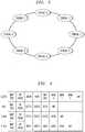
- FIG. 3shows an example of token triggered threading for an implementation of processor 102 in which the number of threads N is eight. In general, all of the threads operate simultaneously, and each accesses a corresponding instance of the thread cache 110 and data memory 112. As shown in FIG. 3 , the eight threads are denoted Thread 0, Thread 1, Thread 2,.. . Thread 7, and are illustrated as being serially interconnected in the form of a ring.
- a given threadcan generally be viewed in terms of hardware as well as software.
- the particular processor hardware associated with a given threadis therefore more particularly referred to herein as a hardware thread unit or simply a "context.”
- token triggered threadingIn accordance with the token triggered threading illustrated in FIG. 3 , all of the hardware thread units or contexts are permitted to simultaneously execute instructions, but only one context may issue an instruction in a particular clock cycle of the processor. In other words, all contexts execute simultaneously but only one context is active on a particular clock cycle. Therefore, if there are a total of C contexts it will require C clock cycles to issue an instruction from all contexts. Each clock cycle, one of the contexts issues an instruction, and the next thread to issue an instruction is indicated by a token. In the FIG. 3 example, the tokens are arranged in a sequential or round-robin manner, such that the contexts will issue instructions sequentially. However, tokens indicating the next context to issue an instruction may be arranged using other patterns, such as an alternating even-odd pattern. Also, as noted above, other types of threading may be used in conjunction with the present invention.
- FIG. 4illustrates the manner in which example instruction functions may be pipelined in the multithreaded processor 102 in accordance with the present invention.
- this type of pipeliningis preferably utilized in conjunction with the token triggered threading described previously, but it is to be appreciated that numerous other combinations of pipelining and threading may be used in implementing the invention.
- the example instruction functions in FIG. 4include Load/Store (Ld/St), ALU, integer multiplication (I_Mul) and vector multiplication (V_Mul), and are shown as having nine, six, seven and eight pipeline stages, respectively.
- Each of the example instruction pipelines illustrated in FIG. 4includes at least an instruction decode stage, a register file (RF) read stage, a transfer (Xfer) stage and a writeback (WB) stage.
- the RF read stageinvolves reading from a register file, e.g., the register file 118
- the transfer stagetypically involves transferring instruction results to a designated holding register
- the WB stageinvolves writing instruction results back to memory or a register file.
- the Ld/St pipelinefurther includes an address generation (Agen) stage, an internal (Int) or external (Ext) determination stage, and three additional memory execute stages, denoted MemO, Mem1 and Mem2.
- the Ld/St pipelinethus includes a total of four memory execute stages, that is, MemO, Mem1, Mem2 and WB.
- the internal or external determination stagedetermines if the associated memory access is to an internal or an external memory, and may be viewed as an additional decode stage within the pipeline. It should be noted that additional memory execute stages may be required for certain external memory accesses. For example, if the WB stage of an external memory access does not complete during the period of time for which the corresponding thread is active, the thread may be stalled such that the WB stage will complete the next time the thread is active.
- the ALU pipelinefurther includes two execution stages denoted Exec1 and Exec2.
- the integer I_Mul pipelinefurther includes three execution stages denoted Exec1, Exec2 and Exec3.
- the vector V_Mul pipelinefurther includes two multiplication stages MPY1 and MPY2, and two addition stages Add1 and Add2.
- the multithreaded processor 102is preferably configured such that once an instruction from a particular context enters its corresponding pipeline, it runs to completion.
- FIGS. 5 and 6each show sequences of instructions issued by particular processor threads, and indicate for each instruction whether an even (e) portion or an odd (o) portion of the register file 118 is utilized by the corresponding thread.
- FIG. 7shows an example of how the register file 118 may be separated into even and odd portions, with a particular one of the portions being selectable utilizing a thread identifier, in accordance with the techniques of the invention.
- each threadissues instructions in accordance with a round-robin implementation of the FIG. 3 token triggered threading. More specifically, each thread in these examples issues alternating Load and Vector Multiply instructions, which is a typical instruction sequence in many signal processing applications.
- the Load and Vector Multiply instructionsare configured substantially as described in accordance with the instruction function pipeline shown in FIG. 4 .
- FIG. 5an example of a single issue pipeline is shown, in which each thread issues one instruction per cycle.
- the register file portions accessed by the issued instructionsalternate from thread to thread between even (e) and odd (o).
- Thisensures that adjacent register writeback operations, such as those associated with the writeback stages of the first Load instruction of Thread 4 and the Vector Multiply instruction of Thread 1, are directed to different portions of the register file. More specifically, the first Load instruction of Thread 4 is directed to an even portion of the register file, while the Vector Multiply instruction of Thread 1 is directed to an odd portion of the register file.
- the other instructions shown in the diagramare similarly configured.
- LSBleast significant bit
- FIG. 6shows an example multiple issue pipeline in which each of the processor threads issues two instructions per cycle.
- a single threadis issuing both Load and Vector Multiply instructions each cycle.
- two additional register file read portsare required relative to the FIG. 5 example.
- all concurrent writesare still to even or odd portions of the register file, as determined based on the LSB of the thread identifier, so the number of required register file write ports and thus the processor power consumption are reduced.
- FIG. 7illustrates the manner in which the register file 118 of the multithreaded processor 102 is configured in accordance with the above-described thread-based register file selection technique of the present invention.
- the register file 118is shown as being associated with processor circuitry 700 which further includes a thread identifier register 702 and selection circuitry 704.
- the register file 118which may be a general-purpose register file or other type of register file associated with processor 102, is configured into a number of even sets of registers and a number of odd sets of registers. More specifically, the register file 118 is divided into an even portion comprising even register sets T 0 and T 2 , and an odd portion comprising odd register sets T 1 and T 3 .
- Each of the eight vector registers V 0 , V 1 , V 2 ... V 7includes in this illustrative example four vector elements of, e.g., 40 bits each.
- the vector register V 7 in register set T 0includes four vector elements denoted V 28 , V 29 , V 30 and V 31 .
- this particular arrangementis provided by way of example only, and numerous other configurations could be used.
- a portion of the thread identifier, as stored in the thread identifier register 702,is utilized to enable either the even sets of registers or the odd sets of registers.
- the selection circuitry 704comprises a multiplexer which drives one of its enable even and enable_odd outputs to a logic high level while the other is driven to a logic low level, based on the thread identifier.
- a register file configuration similar to that illustrated in FIG. 7can also be used with other values of N.
- each of the even and odd portions of the register filecan be configured utilizing only a single write port.
- register file configurationsare possible using the techniques of the invention.
- one possible alternative configurationis to separate the register file into more than two portions, in which case additional bits of the thread identifier may be used to select a particular portion of the register file for access by a given processor thread. More generally, n least significant bits of the thread identifier may be used to select one of 2 n distinct portions of a given register file.
- Another possible alternative configurationis to separate a single register into at least even and odd portions, with thread-based selection of the even or odd portion. More generally, a single register may be separated into 2" distinct portions.
- register fileas used herein is therefore intended to include any arrangement of one or more registers.
- a given register filemay therefore comprise, by way of example and without limitation, one or more general purpose registers, auxiliary registers, branch registers, program registers, etc. as well as portions or combinations thereof.
- the thread identifier register 702 and the associated selection circuitry 704are preferably implemented as elements of the multithreaded processor 102.
- these elementsmay be implemented in whole or in part in the cache controller 114, or in another portion of the multithreaded processor 102.
- the thread identifier register 702stores a multi-bit thread identifier that is used by the multithreaded processor 102 to identify a particular thread. Such thread identifiers may be generated in a conventional manner, as will be apparent to those skilled in the art.
- thread identifieris intended to include any information suitable for identifying a particular thread or a set of multiple threads in a multithreaded processor.
- the thread identifiermay correspond to the output of a thread counter in a multithreaded processor.
- a given multithreaded processormay be configured such that multiple threads are processed in a predetermined order, such as a round robin order, with the thread counter output being used to identify the particular thread being executed. In such an embodiment, there may be a total of eight threads that are processed in round robin order, as illustrated in FIG.
- each threadbeing identified by a three-bit identifier, such that the output of a three-bit counter can be used to identify the particular thread being processed.
- Other embodimentsmay use a non-counter implementation of the thread identifier.
- a wide variety of different thread identifier configurations suitable for use with the present inventionwill be readily apparent to those skilled in the art.
- the thread-based register file selection techniques of the present inventionprovide significant improvements relative to conventional techniques.
- the techniquescan substantially reduce the number of required register file write ports, thereby reducing power consumption.
- these improvementsare provided without impacting processor concurrency or other aspects of processor performance.
- a given register filecan be divided into more than just an even portion and an odd portion as in FIGS. 5 , 6 and 7 , that is, it can be divided into n distinct portions, with an appropriate increase in the number of thread identifier bits used to select a given portion.
- the particular selection circuitry arrangements used to implement the selection processcan be replaced with alternative arrangements.
- the multithreaded processor configuration, the number of threads, the thread identifier configuration and other parameters of the illustrative embodimentscan be varied to accommodate the specific needs of a given application.
Landscapes
- Engineering & Computer Science (AREA)
- Software Systems (AREA)
- Theoretical Computer Science (AREA)
- Physics & Mathematics (AREA)
- General Engineering & Computer Science (AREA)
- General Physics & Mathematics (AREA)
- Multimedia (AREA)
- Advance Control (AREA)
- Executing Machine-Instructions (AREA)
- Debugging And Monitoring (AREA)
- Stored Programmes (AREA)
Description
- The present invention is related to the inventions described in U.S. Patent Applications Attorney Docket No. 1007-5, entitled "Method and Apparatus for Thread-Based Memory Access in a Multithreaded Processor," Attorney Docket No. 1007-6, entitled "Multithreaded Processor With Efficient Processing For Convergence Device Applications," and Attorney Docket No. 1007-8, entitled "Method and Apparatus for Token Triggered Multithreading," all of which are filed concurrently herewith.
- The present invention relates generally to the field of digital data processors, and more particularly to register file access techniques in a multithreaded processor.
- Storage spaces in a computer system or other processor-based system are typically partitioned into memory and registers. Conventional register file configurations are described in, for example,M.J. Flynn, "Computer Architecture: Pipelined and Parallel Processor Design," Jones and Bartlett Publishers, Boston, MA, 1995, andG.A. Blaauw and Frederick P. Brooks, "Computer Architecture: Concepts and Evolution," Addison-Wesley, Reading, Massachusetts, 1997.
- A given register file may be a so-called "general purpose" register file, which typically refers to a register file utilizable for storage of intermediate or otherwise temporary results associated with multiple instruction functions within the processor. Historically, only one instruction would be actively accessing a general purpose register file per processor cycle, such that the number of required register ports was minimal. However, modern processors typically have many instructions active in a given processor cycle, and thus multiple register file accesses per processor cycle. For example, a multithreaded processor provides high concurrency through simultaneous execution of multiple distinct instruction sequences or "threads," with temporary results being stored in register files.
- These and other similar arrangements in modern processors can result in a substantial increase in the "port pressure," that is, the number of required register file ports. Unfortunately, a significant problem associated with register file port pressure is that an increase in the number of register file ports also substantially increases the power dissipation of the processor. Typically, the power consumption associated with register file ports is primarily attributable to the write ports of the register file.
- An example of a modern processor which includes a general purpose register file is the Texas Instruments (TI) C64x, described in the TMS320C6000 CPU and Instruction Set Reference Guide, SPRZ168B, http://www-s.ti.com/sc/psheets/sprz168b/sprz168b.pdf. The TI C64x utilizes a type of Very Long Instruction Word (VLIW) architecture in which up to eight instructions per cycle can issue, with one instruction controlling one execution unit of the processor. The processor register file includes 64 registers. Configuring the C64x such that each instruction can access all 64 registers requires 26 read ports and 18 write ports, for a total of 44 ports. However, since such an arrangement is intractable, the designers of the C64x instead decided to split the register file access in half, thereby placing restrictions on the programmer, while dividing the ports between the two halves. Nonetheless, the C64x still requires a total of 44 ports.
- Reducing port pressure is thus an important aspect of modern processor design, particularly for multithreaded processors and other processors in which many instructions may be active in a given processor cycle. A need exists in the art for techniques for providing reductions in port pressure, so as to decrease processor power consumption, without impacting the desired level of concurrency.
- US patent application
US 2002/103990 discloses an architecture and an operation method for a computer processor supporting interleaved execution of multiple concurrently-active threads using thread identifiers to for selecting memory banks which are provided individually for each thread. Further related operation methods for multithreaded processors are disclosed in US patentUS 5 778 243 A and in the scientific articleJ. W. Haskins et al., "Inexpensive Throughput Enhancement in Small-Scale Embedded Microprocessors with Block Multithreading: Extensions, Characterization, and Tradeoffs", Proc. of the 2001 IEEE International Performance, Computing, and Communications Conference (IPCCC), Phoenix, AZ, April 4-6, 2001, IEEE New York, NY, US, Vol. Conf. 20, 4 April 2001, pp. 319-328, ISBN: 0-7803-7001-5. - The present invention provides an improved register file configuration and associated thread-based register file selection technique for a multithreaded processor.
- In accordance with the invention, a multithreaded processor determines a thread identifier associated with a particular processor thread, and utilizes at least a portion of the thread identifier to select a particular portion of a register file to be accessed by the corresponding processor thread. For example, a least significant bit or other portion of the thread identifier may be utilized to select one of an even portion and an odd portion of the register file.
- As a more particular example, a given general purpose register file may be configured into a plurality of even sets of registers and a plurality of odd sets of registers, witb a portion of the thread identifier being utilized to enable either the plurality of even sets of registers or the plurality of odd sets of registers.
- Other aspects of the invention relate to token triggered threading and pipelined instruction processing. For example, the multithreaded processor may be configured to implement token triggered threading. This type of threading utilizes a token to identify, in association with a current processor clock cycle, a particular hardware thread unit or context that will be permitted to issue an instruction for a subsequent clock cycle.
- Advantageously, the invention significantly reduces the number of required register file write ports, and thus reduces processor power consumption, without any loss of processor performance. For example, in the illustrative embodiment, multiple write accesses to the register file can be achieved in a single processor cycle using only a single write port.
FIG. 1 is a block diagram of an example processing system in which the invention is implemented.FIG. 2 is a more detailed block diagram of an illustrative embodiment of a multithreaded processor of theFIG. 1 processing system.FIG. 3 illustrates an example of token triggered threading suitable for use in the multithreaded processor ofFIG. 2 in accordance with the techniques of the invention.FIG. 4 illustrates the manner in which example instruction functions may be pipelined in theFIG. 2 multithreaded processor in accordance with the techniques of the invention.FIG. 5 shows an example single issue pipeline in which each of the threads of theFIG. 2 processor issues one instruction per cycle.FIG. 6 shows an example multiple issue pipeline in which each of the threads of theFIG. 2 processor issues two instructions per cycle.FIG. 7 shows a register file of theFIG. 2 processor configured in accordance with a thread-based register file selection technique of the present invention.- The present invention will be illustrated herein as implemented in a multithreaded processor having associated therewith a general purpose register file. It should be understood, however, that the invention does not require the use of the particular multithreaded processor and register file configurations of the illustrative embodiment, and is more generally suitable for use in any multithreaded processor register file application in which it is desirable to provide a reduction in the number of required register file write ports and thus reduced power consumption.
- An
example processing system 100 which implements a thread-based register file selection technique in accordance with the invention will be described in conjunction withFIGS. 1 and 2 . FIG. 1 shows theprocessing system 100 as including amultithreaded processor 102 coupled to amain memory 104. The multithreadedprocessor 102 includes a multithreadedcache memory 110 and a multithreadeddata memory 112.FIG. 2 shows a more detailed view of one possible implementation of themultithreaded processor 102. In this embodiment, themultithreaded processor 102 includes themultithreaded cache memory 110, thedata memory 112, acache controller 114, aninstruction decoder 116, aregister file 118, and a set of arithmetic logic units (ALUs) 120. The multithreadedcache memory 110 is also referred to herein as a multithreaded cache.- It should be noted that the particular arrangements shown in
FIGS. 1 and 2 are simplified for clarity of illustration, and additional or alternative elements not explicitly shown may be included, as will be apparent to those skilled in the art. - The
multithreaded cache 110 includes a plurality of thread caches 110-1, 110-2, ... 110-N, where N generally denotes the number of threads supported by themultithreaded processor 102. Each thread thus has a corresponding thread cache associated therewith in themultithreaded cache 110. Similarly, thedata memory 112 includes N distinct data memory instances, denoted data memories 112-1, 112-2, ... 112-N as shown. - Each of the thread caches in the
multithreaded cache 110 may comprise a memory array having one or more sets of memory locations. A given thread cache may further comprise a thread identifier register for storing an associated thread identifier, as will be described in greater detail below in conjunction withFIG. 7 . - The
multithreaded cache 110 interfaces with themain memory 104 via thecache controller 114. Thecache controller 114 ensures that the appropriate instructions frommain memory 104 are loaded into themultithreaded cache 110. Thecache controller 114 in this illustrative embodiment, operating in conjunction with logic circuitry or other processing elements associated with the individual thread caches 110-1, 110-2, ... 110-N, implements at least a portion of an address mapping technique, such as fully associative mapping, direct mapping or set-associative mapping. Illustrative set-associative mapping techniques suitable for use in conjunction with the present invention are described inU.S. Patent Application Serial Nos. 10/161,774 10/161,874 - In general, the
multithreaded cache 110 is used to store instructions to be executed by themultithreaded processor 102, while thedata memory 112 stores data that is operated on by the instructions. Instructions are fetched from themultithreaded cache 110 by theinstruction decoder 116 which operates in conjunction with theregister file 118 and theALUs 120 in controlling the execution of the instructions in a conventional manner. The operation of multithreaded processor elements such as 116 and 120 is well-understood in the art, and therefore not described in further detail herein. - The
data memory 112 is typically directly connected to themain memory 104, although this connection is not explicitly shown in the figure. - One or more of the
memories - Techniques for thread-based banking of these and other memories associated with a multithreaded processor are described in the above-cited U.S. Patent Application Attorney Docket No. 1007-5, entitled "Method and Apparatus for Thread-Based Memory Access in a Multithreaded Processor."
- It should be emphasized that the present invention does not require the particular multithreaded processor configuration shown in
FIG. 2 . The invention can be implemented in a wide variety of other multithreaded processor configurations. - A more particular example of multithreaded processor of the type shown in
FIG. 2 and suitable for use in conjunction with the present invention is described inU.S. Provisional Application Serial No. 60/341,289, filed December 20, 2001 U.S. Provisional Application Serial No. 60/341,289 is capable of executing RISC-based control code, digital signal processor (DSP) code, Java code and network processing code. The processor includes a single instruction multiple data (SIMD) vector unit, a reduction unit, and long instruction word (LIW) compounded instruction execution. - The present invention in accordance with one aspect thereof provides a substantial reduction in the register file port requirements of a multithreaded processor such as
processor 102 ofFIG. 2 . More specifically, as will be described in greater detail below, theprocessor 102 is configured in accordance with the techniques of the invention to utilize a thread-based partitioning of the register file in conjunction with token triggered threading and instruction pipelining to reduce the register file port requirements. Among other advantages, this configuration allows multiple simultaneous writes to be supported by a single register file write port. FIG. 3 shows an example of token triggered threading for an implementation ofprocessor 102 in which the number of threads N is eight. In general, all of the threads operate simultaneously, and each accesses a corresponding instance of thethread cache 110 anddata memory 112. As shown inFIG. 3 , the eight threads are denotedThread 0,Thread 1,Thread 2,.. .Thread 7, and are illustrated as being serially interconnected in the form of a ring. In the multithreaded processor, a given thread can generally be viewed in terms of hardware as well as software. The particular processor hardware associated with a given thread is therefore more particularly referred to herein as a hardware thread unit or simply a "context."- In accordance with the token triggered threading illustrated in
FIG. 3 , all of the hardware thread units or contexts are permitted to simultaneously execute instructions, but only one context may issue an instruction in a particular clock cycle of the processor. In other words, all contexts execute simultaneously but only one context is active on a particular clock cycle. Therefore, if there are a total of C contexts it will require C clock cycles to issue an instruction from all contexts. Each clock cycle, one of the contexts issues an instruction, and the next thread to issue an instruction is indicated by a token. In theFIG. 3 example, the tokens are arranged in a sequential or round-robin manner, such that the contexts will issue instructions sequentially. However, tokens indicating the next context to issue an instruction may be arranged using other patterns, such as an alternating even-odd pattern. Also, as noted above, other types of threading may be used in conjunction with the present invention. FIG. 4 illustrates the manner in which example instruction functions may be pipelined in themultithreaded processor 102 in accordance with the present invention. In the illustrative embodiment of the invention, this type of pipelining is preferably utilized in conjunction with the token triggered threading described previously, but it is to be appreciated that numerous other combinations of pipelining and threading may be used in implementing the invention.- The
FIG. 4 pipeline is configured for use in conjunction with the illustrative N = 8 token triggered threading ofFIG. 3 . The example instruction functions inFIG. 4 include Load/Store (Ld/St), ALU, integer multiplication (I_Mul) and vector multiplication (V_Mul), and are shown as having nine, six, seven and eight pipeline stages, respectively. - Each of the example instruction pipelines illustrated in
FIG. 4 includes at least an instruction decode stage, a register file (RF) read stage, a transfer (Xfer) stage and a writeback (WB) stage. The RF read stage involves reading from a register file, e.g., theregister file 118, the transfer stage typically involves transferring instruction results to a designated holding register, and the WB stage involves writing instruction results back to memory or a register file. - The Ld/St pipeline further includes an address generation (Agen) stage, an internal (Int) or external (Ext) determination stage, and three additional memory execute stages, denoted MemO, Mem1 and Mem2. The Ld/St pipeline thus includes a total of four memory execute stages, that is, MemO, Mem1, Mem2 and WB. The internal or external determination stage determines if the associated memory access is to an internal or an external memory, and may be viewed as an additional decode stage within the pipeline. It should be noted that additional memory execute stages may be required for certain external memory accesses. For example, if the WB stage of an external memory access does not complete during the period of time for which the corresponding thread is active, the thread may be stalled such that the WB stage will complete the next time the thread is active.
- The ALU pipeline further includes two execution stages denoted Exec1 and Exec2.
- The integer I_Mul pipeline further includes three execution stages denoted Exec1, Exec2 and Exec3.
- The vector V_Mul pipeline further includes two multiplication stages MPY1 and MPY2, and two addition stages Add1 and Add2.
- The
multithreaded processor 102 is preferably configured such that once an instruction from a particular context enters its corresponding pipeline, it runs to completion. - With an appropriately-configured pipeline and a sufficient number of threads, all hardware contexts may be executing concurrently even though there is only a single instruction issued per context per cycle. As indicated previously, the particular number of threads and pipeline stages are purposes of illustration only, and not intended to reflect a preferred implementation. Those skilled in the art will be readily able to determine an appropriate number of threads and pipeline stages for a particular application given the teachings provided herein.
- A number of examples of the operation of the pipeline of
FIG. 4 will now be described with reference toFIGS. 5 and6 . The drawings ofFIGS. 5 and6 each show sequences of instructions issued by particular processor threads, and indicate for each instruction whether an even (e) portion or an odd (o) portion of theregister file 118 is utilized by the corresponding thread.FIG. 7 shows an example of how theregister file 118 may be separated into even and odd portions, with a particular one of the portions being selectable utilizing a thread identifier, in accordance with the techniques of the invention. - In the examples of
FIGS. 5 and6 , it is assumed for simplicity and clarity of description that the number of threads N is equal to 4, and that each thread issues instructions in accordance with a round-robin implementation of theFIG. 3 token triggered threading. More specifically, each thread in these examples issues alternating Load and Vector Multiply instructions, which is a typical instruction sequence in many signal processing applications. The Load and Vector Multiply instructions are configured substantially as described in accordance with the instruction function pipeline shown inFIG. 4 . - Referring now to
FIG. 5 , an example of a single issue pipeline is shown, in which each thread issues one instruction per cycle. It can be seen from theFIG. 5 diagram that the register file portions accessed by the issued instructions alternate from thread to thread between even (e) and odd (o). This ensures that adjacent register writeback operations, such as those associated with the writeback stages of the first Load instruction ofThread 4 and the Vector Multiply instruction ofThread 1, are directed to different portions of the register file. More specifically, the first Load instruction ofThread 4 is directed to an even portion of the register file, while the Vector Multiply instruction ofThread 1 is directed to an odd portion of the register file. The other instructions shown in the diagram are similarly configured. - As will be described in conjunction with
FIG. 7 , the thread identifier is used to select whether the even portion or the odd portion of the register file will be accessed by a given thread. For example, in the N = 4 case ofFIGS. 5 and6 , the least significant bit (LSB) of the thread identifier can be used to select between the even and odd portions of the register file. FIG. 6 shows an example multiple issue pipeline in which each of the processor threads issues two instructions per cycle. Here, a single thread is issuing both Load and Vector Multiply instructions each cycle. Because multiple instructions issue per cycle, two additional register file read ports are required relative to theFIG. 5 example. However, as can be seen in the diagram, all concurrent writes are still to even or odd portions of the register file, as determined based on the LSB of the thread identifier, so the number of required register file write ports and thus the processor power consumption are reduced.- It should be emphasized that the particular number of threads shown in conjunction with
FIGS. 5 and6 is by way of example only, and the invention is not limited to use with any particular thread number. FIG. 7 illustrates the manner in which theregister file 118 of themultithreaded processor 102 is configured in accordance with the above-described thread-based register file selection technique of the present invention. Theregister file 118 is shown as being associated withprocessor circuitry 700 which further includes athread identifier register 702 andselection circuitry 704. In this embodiment, theregister file 118, which may be a general-purpose register file or other type of register file associated withprocessor 102, is configured into a number of even sets of registers and a number of odd sets of registers. More specifically, theregister file 118 is divided into an even portion comprising even register sets T0 and T2, and an odd portion comprising odd register sets T1 and T3.- Each of the register sets T0, T1, T2 and T3 corresponds generally to one of four threads in an N = 4 embodiment, and includes eight vector registers V0, V1, V2 ... V7 as shown. Each of the eight vector registers V0, V1, V2 ... V7 includes in this illustrative example four vector elements of, e.g., 40 bits each. For example, the vector register V7 in register set T0 includes four vector elements denoted V28, V29, V30 and V31. Of course, this particular arrangement is provided by way of example only, and numerous other configurations could be used.
- A portion of the thread identifier, as stored in the
thread identifier register 702, is utilized to enable either the even sets of registers or the odd sets of registers. Theselection circuitry 704 comprises a multiplexer which drives one of its enable even and enable_odd outputs to a logic high level while the other is driven to a logic low level, based on the thread identifier. - A register file configuration similar to that illustrated in
FIG. 7 can also be used with other values of N. For example, this configuration may be used in an N = 8 embodiment, with an additional bit of the thread identifier being utilized in the selection process. - The above-described arrangement allows the
register file 118 to include a significantly reduced number of write ports, and thus lower power consumption, than that which would otherwise be required using conventional techniques. In the particular arrangement shown inFIG. 7 , and for a four-thread implementation, each of the even and odd portions of the register file can be configured utilizing only a single write port. - Numerous alternative register file configurations are possible using the techniques of the invention. For example, one possible alternative configuration is to separate the register file into more than two portions, in which case additional bits of the thread identifier may be used to select a particular portion of the register file for access by a given processor thread. More generally,n least significant bits of the thread identifier may be used to select one of 2n distinct portions of a given register file.
- Another possible alternative configuration is to separate a single register into at least even and odd portions, with thread-based selection of the even or odd portion. More generally, a single register may be separated into 2" distinct portions.
- The term "register file" as used herein is therefore intended to include any arrangement of one or more registers. A given register file may therefore comprise, by way of example and without limitation, one or more general purpose registers, auxiliary registers, branch registers, program registers, etc. as well as portions or combinations thereof.
- The
thread identifier register 702 and the associatedselection circuitry 704 are preferably implemented as elements of themultithreaded processor 102. For example, these elements may be implemented in whole or in part in thecache controller 114, or in another portion of themultithreaded processor 102. - The
thread identifier register 702 stores a multi-bit thread identifier that is used by themultithreaded processor 102 to identify a particular thread. Such thread identifiers may be generated in a conventional manner, as will be apparent to those skilled in the art. - The term "thread identifier" as used herein is intended to include any information suitable for identifying a particular thread or a set of multiple threads in a multithreaded processor. By way of example and without limitation, the thread identifier may correspond to the output of a thread counter in a multithreaded processor. More particularly, a given multithreaded processor may be configured such that multiple threads are processed in a predetermined order, such as a round robin order, with the thread counter output being used to identify the particular thread being executed. In such an embodiment, there may be a total of eight threads that are processed in round robin order, as illustrated in
FIG. 3 , with each thread being identified by a three-bit identifier, such that the output of a three-bit counter can be used to identify the particular thread being processed. Other embodiments may use a non-counter implementation of the thread identifier. A wide variety of different thread identifier configurations suitable for use with the present invention will be readily apparent to those skilled in the art. - As indicated above, the thread-based register file selection techniques of the present invention provide significant improvements relative to conventional techniques. For example, the techniques can substantially reduce the number of required register file write ports, thereby reducing power consumption. Moreover, these improvements are provided without impacting processor concurrency or other aspects of processor performance.
- The above-described embodiments of the invention are intended to be illustrative only, and numerous alternative embodiments within the scope of the appended claims will be apparent to those skilled in the art. For example, as indicated previously, a given register file can be divided into more than just an even portion and an odd portion as in
FIGS. 5 ,6 and7 , that is, it can be divided into n distinct portions, with an appropriate increase in the number of thread identifier bits used to select a given portion. As another example, the particular selection circuitry arrangements used to implement the selection process can be replaced with alternative arrangements. Moreover, the multithreaded processor configuration, the number of threads, the thread identifier configuration and other parameters of the illustrative embodiments can be varied to accommodate the specific needs of a given application.
Claims (20)
- A method for accessing a register file (118) associated with a multithreaded processor (102), the multithreaded processor having a cache memory (110), the method comprising:determining a thread identifier associated with a particular thread of the multithreaded processor;selecting a particular one out of separate portions of the register file (T0-T3) to be accessed by the corresponding processor thread based on token triggered threading utilizing at least a portion of the thread identifier;wherein the register file is separate from the cache memory of the multithreaded processor;wherein the cache memory fetches instructions through an instruction decoder; andwherein the separate portions of the register file are accessed by the threads of the multithreaded processor alternatingly over a plurality of processor clock cycles such that register accesses by odd-numbered threads are directed to different portions of the register file as compared to even-numbered threads.
- The method of claim 1 wherein utilizing a portion of the thread identifier comprises utilizing a portion of the thread identifier to select one of a first portion and a second portion of the register file for access by the corresponding processor thread.
- The method of claim 2 wherein selecting portions of the register file comprises utilizing a least significant bit of the thread identifier.
- The method of claim 2, wherein the register file comprises a plurality of register sets, and the utilizing step further comprises enabling either a first plurality of sets of registers or a second plurality of sets of registers for access by the corresponding processor thread.
- The method of claim 1 wherein selecting portions of the register file comprises applying the portion of the thread identifier to selection circuitry configured to generate enable signals for the selected portions of the register file.
- The method of claim 1 wherein the register file comprises 2n distinct portions, and n least significant bits of the thread identifier are utilized to select one of the 2n distinct portions of the register file for access by the corresponding processor thread.
- The method of claim 1 wherein accessing the register file comprises accessing a portion of a general-purpose register file.
- The method of claim 1 wherein determining a thread identifier associated with a particular thread of the multithreaded processor comprises accessing a thread identifier register storing the thread identifier.
- The method of claim 8, wherein accessing the thread identifier register comprises accessing a thread identifier register associated with a thread cache corresponding to the particular thread of the multithreaded processor.
- The method of claim 1 wherein the token triggered threading comprises utilizing a token to identify in association with a current processor clock cycle a particular context that will be permitted to issue an instruction for a subsequent clock cycle.
- The method of claim 1 wherein the token triggered threading comprises assigning different tokens to each of a plurality of threads of the multithreaded processor.
- The method of claim 1 further comprising processing pipelined instructions.
- The method of claim 12 wherein processing pipelined instructions utilizes an instruction pipeline in which each thread issues a single instruction per processor clock cycle.
- The method of claim 12, wherein the multithreaded processor utilizes an instruction pipeline in which each thread issues multiple instructions per processor clock cycle.
- The method of claim 14 wherein each of a plurality of the threads issues both a load instruction and a vector multiply instruction in each of a corresponding plurality of processor clock cycles without stalling of any of the plurality of threads.
- The method of claim 1 wherein accessing the register file either comprises accessing a single register or accessing a plurality of registers.
- The method of claim 1 wherein each of N threads is sequentially accessed in each clock cycle until the N-th thread is accessed.
- The method of claim 1 wherein first and second threads are accessed in a clock cycle, third and fourth threads are accessed in a next clock cycle until N-1-th and N-th threads are accessed sequentially in each subsequent clock cycle.
- A multithreaded processor (102) having an associated register file (118) comprising separate portions, the multithreaded processor further having a cache memory (110),
wherein the multithreaded processor is operative to determine a thread identifier associated with a particular thread of the multithreaded processor, and to select a particular one out of the separate portions of the register file (T0-T3) thread based on token triggered threading by utilizing at least a portion of the thread identifier,
wherein the register file is separate from the cache memory of the multithreaded processor,
wherein the cache memory fetches instructions through an instruction decoder; and
wherein the multithreaded processor is adapted to control its threads such as to access the separate portions of the register file alternatingly over a plurality of processor clock cycles such that register accesses by odd-numbered threads are directed to different portions of the register file as compared to even-numbered threads. - An article of manufacture comprising a machine-readable storage medium having embodied thereon program code for use in accessing a register file (118) associated with a multithreaded processor (102), the multithreaded processor having a cache memory (110), wherein the program code when executed by the processor implements the steps of:determining a thread identifier associated with a particular thread of the multithreaded processor; andselecting a particular one out of separate portions of the register file (T0-T3) to be accessed by the corresponding processor thread based on token triggered threading utilizing at least a portion of the thread identifier;wherein the register file is separate from the cache memory of the multithreaded processor;wherein the cache memory fetches instructions through an instruction decoder; andwherein the separate portions of the register file are accessed by the threads of the multithreaded processor alternatingly over a plurality of processor clock cycles such that register accesses by odd-numbered threads are directed to different portions of the register file as compared to even-numbered threads.
Priority Applications (1)
| Application Number | Priority Date | Filing Date | Title |
|---|---|---|---|
| EP13001004.4AEP2600242A1 (en) | 2002-10-11 | 2003-10-09 | Method and apparatus for register file port reduction in a multithreaded processor |
Applications Claiming Priority (3)
| Application Number | Priority Date | Filing Date | Title |
|---|---|---|---|
| US269373 | 1988-11-10 | ||
| US10/269,373US6904511B2 (en) | 2002-10-11 | 2002-10-11 | Method and apparatus for register file port reduction in a multithreaded processor |
| PCT/US2003/031904WO2004034209A2 (en) | 2002-10-11 | 2003-10-09 | Method and apparatus for register file port reduction in a multithreaded processor |
Related Child Applications (1)
| Application Number | Title | Priority Date | Filing Date |
|---|---|---|---|
| EP13001004.4ADivision-IntoEP2600242A1 (en) | 2002-10-11 | 2003-10-09 | Method and apparatus for register file port reduction in a multithreaded processor |
Publications (3)
| Publication Number | Publication Date |
|---|---|
| EP1550030A2 EP1550030A2 (en) | 2005-07-06 |
| EP1550030A4 EP1550030A4 (en) | 2008-03-05 |
| EP1550030B1true EP1550030B1 (en) | 2020-11-18 |
Family
ID=32068767
Family Applications (2)
| Application Number | Title | Priority Date | Filing Date |
|---|---|---|---|
| EP03774678.1AExpired - LifetimeEP1550030B1 (en) | 2002-10-11 | 2003-10-09 | Method and apparatus for register file port reduction in a multithreaded processor |
| EP13001004.4ACeasedEP2600242A1 (en) | 2002-10-11 | 2003-10-09 | Method and apparatus for register file port reduction in a multithreaded processor |
Family Applications After (1)
| Application Number | Title | Priority Date | Filing Date |
|---|---|---|---|
| EP13001004.4ACeasedEP2600242A1 (en) | 2002-10-11 | 2003-10-09 | Method and apparatus for register file port reduction in a multithreaded processor |
Country Status (8)
| Country | Link |
|---|---|
| US (1) | US6904511B2 (en) |
| EP (2) | EP1550030B1 (en) |
| JP (1) | JP4187720B2 (en) |
| KR (1) | KR100988955B1 (en) |
| CN (1) | CN100342325C (en) |
| AU (1) | AU2003282486A1 (en) |
| ES (1) | ES2848383T3 (en) |
| WO (1) | WO2004034209A2 (en) |
Families Citing this family (51)
| Publication number | Priority date | Publication date | Assignee | Title |
|---|---|---|---|---|
| US20040193846A1 (en)* | 2003-03-28 | 2004-09-30 | Sprangle Eric A. | Method and apparatus for utilizing multiple opportunity ports in a processor pipeline |
| EP2290525A3 (en) | 2003-05-09 | 2011-04-20 | Aspen Acquisition Corporation | Processor reduction unit for accumulation of multiple operands with or without saturation |
| US7475222B2 (en)* | 2004-04-07 | 2009-01-06 | Sandbridge Technologies, Inc. | Multi-threaded processor having compound instruction and operation formats |
| US7797363B2 (en)* | 2004-04-07 | 2010-09-14 | Sandbridge Technologies, Inc. | Processor having parallel vector multiply and reduce operations with sequential semantics |
| US8074051B2 (en) | 2004-04-07 | 2011-12-06 | Aspen Acquisition Corporation | Multithreaded processor with multiple concurrent pipelines per thread |
| US7890735B2 (en)* | 2004-08-30 | 2011-02-15 | Texas Instruments Incorporated | Multi-threading processors, integrated circuit devices, systems, and processes of operation and manufacture |
| TW200625097A (en)* | 2004-11-17 | 2006-07-16 | Sandbridge Technologies Inc | Data file storing multiple date types with controlled data access |
| US20060230253A1 (en)* | 2005-04-11 | 2006-10-12 | Lucian Codrescu | Unified non-partitioned register files for a digital signal processor operating in an interleaved multi-threaded environment |
| US8713286B2 (en)* | 2005-04-26 | 2014-04-29 | Qualcomm Incorporated | Register files for a digital signal processor operating in an interleaved multi-threaded environment |
| US20070223599A1 (en)* | 2005-07-25 | 2007-09-27 | Sysair, Inc., A Delaware Corporation | Cellular PC modem architecture and method of operation |
| KR20090078790A (en)* | 2006-09-26 | 2009-07-20 | 샌드브리지 테크놀로지스, 인코포레이티드 | Software implementation of matrix inversion in a wireless communication system |
| WO2008060948A2 (en)* | 2006-11-10 | 2008-05-22 | Sandbridge Technologies, Inc. | Method and system for parallelization of pipelined computations |
| US20080276067A1 (en)* | 2007-05-01 | 2008-11-06 | Via Technologies, Inc. | Method and Apparatus for Page Table Pre-Fetching in Zero Frame Display Channel |
| US8677101B2 (en)* | 2007-06-07 | 2014-03-18 | International Business Machines Corporation | Method and apparatus for cooperative software multitasking in a processor system with a partitioned register file |
| WO2008155799A1 (en) | 2007-06-20 | 2008-12-24 | Fujitsu Limited | Instruction execution controller and instruction execution control method |
| JP5104863B2 (en) | 2007-06-20 | 2012-12-19 | 富士通株式会社 | Arithmetic processing device and control method of arithmetic processing device |
| US8224884B2 (en)* | 2007-07-06 | 2012-07-17 | XMOS Ltd. | Processor communication tokens |
| US8725991B2 (en)* | 2007-09-12 | 2014-05-13 | Qualcomm Incorporated | Register file system and method for pipelined processing |
| EP2602710A1 (en)* | 2007-11-05 | 2013-06-12 | Aspen Acquisition Corporation | Method of encoding register instruction fields |
| WO2009097444A1 (en)* | 2008-01-30 | 2009-08-06 | Sandbridge Technologies, Inc. | Method for enabling multi-processor synchronization |
| US20100031007A1 (en)* | 2008-02-18 | 2010-02-04 | Sandbridge Technologies, Inc. | Method to accelerate null-terminated string operations |
| EP2266038A4 (en)* | 2008-03-13 | 2011-09-21 | Aspen Acquisition Corp | Method for achieving power savings by disabling a valid array |
| KR20110050665A (en) | 2008-08-06 | 2011-05-16 | 아스펜 액퀴지션 코포레이션 | Stoppable and Restartable DMA Engine |
| US9207995B2 (en) | 2010-11-03 | 2015-12-08 | International Business Machines Corporation | Mechanism to speed-up multithreaded execution by register file write port reallocation |
| JP5283739B2 (en)* | 2011-09-27 | 2013-09-04 | インテル・コーポレーション | Multi-thread communication within the processor |
| US9323528B2 (en)* | 2012-12-20 | 2016-04-26 | Intel Corporation | Method, apparatus, system creating, executing and terminating mini-threads |
| GB2501791B (en) | 2013-01-24 | 2014-06-11 | Imagination Tech Ltd | Register file having a plurality of sub-register files |
| US9508112B2 (en) | 2013-07-31 | 2016-11-29 | Apple Inc. | Multi-threaded GPU pipeline |
| US9377968B2 (en) | 2013-11-13 | 2016-06-28 | Sandisk Technologies Llc | Method and system for using templates to communicate with non-volatile memory |
| US9390033B2 (en) | 2013-11-13 | 2016-07-12 | Sandisk Technologies Llc | Method and system for communicating with non-volatile memory via multiple data paths |
| US9430411B2 (en) | 2013-11-13 | 2016-08-30 | Sandisk Technologies Llc | Method and system for communicating with non-volatile memory |
| GB2520731B (en)* | 2013-11-29 | 2017-02-08 | Imagination Tech Ltd | Soft-partitioning of a register file cache |
| US9594660B2 (en) | 2014-03-27 | 2017-03-14 | International Business Machines Corporation | Multithreading computer system and program product for executing a query instruction for idle time accumulation among cores |
| US10102004B2 (en) | 2014-03-27 | 2018-10-16 | International Business Machines Corporation | Hardware counters to track utilization in a multithreading computer system |
| US9921848B2 (en)* | 2014-03-27 | 2018-03-20 | International Business Machines Corporation | Address expansion and contraction in a multithreading computer system |
| US9804846B2 (en) | 2014-03-27 | 2017-10-31 | International Business Machines Corporation | Thread context preservation in a multithreading computer system |
| EP3131004A4 (en)* | 2014-04-11 | 2017-11-08 | Murakumo Corporation | Processor and method |
| US10514911B2 (en) | 2014-11-26 | 2019-12-24 | International Business Machines Corporation | Structure for microprocessor including arithmetic logic units and an efficiency logic unit |
| US11544214B2 (en)* | 2015-02-02 | 2023-01-03 | Optimum Semiconductor Technologies, Inc. | Monolithic vector processor configured to operate on variable length vectors using a vector length register |
| US11294815B2 (en)* | 2015-06-10 | 2022-04-05 | Mobileye Vision Technologies Ltd. | Multiple multithreaded processors with shared data cache |
| US10338920B2 (en) | 2015-12-18 | 2019-07-02 | Intel Corporation | Instructions and logic for get-multiple-vector-elements operations |
| US20170177351A1 (en)* | 2015-12-18 | 2017-06-22 | Intel Corporation | Instructions and Logic for Even and Odd Vector Get Operations |
| CN114489792B (en)* | 2021-03-25 | 2022-10-11 | 沐曦集成电路(上海)有限公司 | Processor device and instruction execution method thereof |
| US12190116B2 (en) | 2022-04-05 | 2025-01-07 | Simplex Micro, Inc. | Microprocessor with time count based instruction execution and replay |
| US12169716B2 (en) | 2022-04-20 | 2024-12-17 | Simplex Micro, Inc. | Microprocessor with a time counter for statically dispatching extended instructions |
| US12141580B2 (en) | 2022-04-20 | 2024-11-12 | Simplex Micro, Inc. | Microprocessor with non-cacheable memory load prediction |
| US12106114B2 (en) | 2022-04-29 | 2024-10-01 | Simplex Micro, Inc. | Microprocessor with shared read and write buses and instruction issuance to multiple register sets in accordance with a time counter |
| US12288065B2 (en) | 2022-04-29 | 2025-04-29 | Simplex Micro, Inc. | Microprocessor with odd and even register sets |
| US12112172B2 (en) | 2022-06-01 | 2024-10-08 | Simplex Micro, Inc. | Vector coprocessor with time counter for statically dispatching instructions |
| US12147812B2 (en) | 2022-07-13 | 2024-11-19 | Simplex Micro, Inc. | Out-of-order execution of loop instructions in a microprocessor |
| US12282772B2 (en) | 2022-07-13 | 2025-04-22 | Simplex Micro, Inc. | Vector processor with vector data buffer |
Family Cites Families (23)
| Publication number | Priority date | Publication date | Assignee | Title |
|---|---|---|---|---|
| US5226131A (en)* | 1989-12-27 | 1993-07-06 | The United States Of America As Represented By The United States Department Of Energy | Sequencing and fan-out mechanism for causing a set of at least two sequential instructions to be performed in a dataflow processing computer |
| US5404469A (en)* | 1992-02-25 | 1995-04-04 | Industrial Technology Research Institute | Multi-threaded microprocessor architecture utilizing static interleaving |
| US5682491A (en) | 1994-12-29 | 1997-10-28 | International Business Machines Corporation | Selective processing and routing of results among processors controlled by decoding instructions using mask value derived from instruction tag and processor identifier |
| US6128720A (en) | 1994-12-29 | 2000-10-03 | International Business Machines Corporation | Distributed processing array with component processors performing customized interpretation of instructions |
| US5649135A (en) | 1995-01-17 | 1997-07-15 | International Business Machines Corporation | Parallel processing system and method using surrogate instructions |
| US5659785A (en) | 1995-02-10 | 1997-08-19 | International Business Machines Corporation | Array processor communication architecture with broadcast processor instructions |
| US6038643A (en)* | 1996-01-24 | 2000-03-14 | Sun Microsystems, Inc. | Stack management unit and method for a processor having a stack |
| US5778243A (en)* | 1996-07-03 | 1998-07-07 | International Business Machines Corporation | Multi-threaded cell for a memory |
| US6073159A (en)* | 1996-12-31 | 2000-06-06 | Compaq Computer Corporation | Thread properties attribute vector based thread selection in multithreading processor |
| US6128641A (en)* | 1997-09-12 | 2000-10-03 | Siemens Aktiengesellschaft | Data processing unit with hardware assisted context switching capability |
| US6079010A (en) | 1998-03-31 | 2000-06-20 | Lucent Technologies Inc. | Multiple machine view execution in a computer system |
| US6317821B1 (en) | 1998-05-18 | 2001-11-13 | Lucent Technologies Inc. | Virtual single-cycle execution in pipelined processors |
| US6209066B1 (en)* | 1998-06-30 | 2001-03-27 | Sun Microsystems, Inc. | Method and apparatus for memory allocation in a multi-threaded virtual machine |
| US6260189B1 (en) | 1998-09-14 | 2001-07-10 | Lucent Technologies Inc. | Compiler-controlled dynamic instruction dispatch in pipelined processors |
| US6256725B1 (en) | 1998-12-04 | 2001-07-03 | Agere Systems Guardian Corp. | Shared datapath processor utilizing stack-based and register-based storage spaces |
| US6230251B1 (en) | 1999-03-22 | 2001-05-08 | Agere Systems Guardian Corp. | File replication methods and apparatus for reducing port pressure in a clustered processor |
| US6282585B1 (en) | 1999-03-22 | 2001-08-28 | Agere Systems Guardian Corp. | Cooperative interconnection for reducing port pressure in clustered microprocessors |
| US6269437B1 (en) | 1999-03-22 | 2001-07-31 | Agere Systems Guardian Corp. | Duplicator interconnection methods and apparatus for reducing port pressure in a clustered processor |
| US6341347B1 (en)* | 1999-05-11 | 2002-01-22 | Sun Microsystems, Inc. | Thread switch logic in a multiple-thread processor |
| US6542991B1 (en)* | 1999-05-11 | 2003-04-01 | Sun Microsystems, Inc. | Multiple-thread processor with single-thread interface shared among threads |
| US6643747B2 (en)* | 2000-12-27 | 2003-11-04 | Intel Corporation | Processing requests to efficiently access a limited bandwidth storage area |
| US20020103990A1 (en)* | 2001-02-01 | 2002-08-01 | Hanan Potash | Programmed load precession machine |
| US7487505B2 (en)* | 2001-08-27 | 2009-02-03 | Intel Corporation | Multithreaded microprocessor with register allocation based on number of active threads |
- 2002
- 2002-10-11USUS10/269,373patent/US6904511B2/ennot_activeExpired - Lifetime
- 2003
- 2003-10-09WOPCT/US2003/031904patent/WO2004034209A2/enactiveApplication Filing
- 2003-10-09EPEP03774678.1Apatent/EP1550030B1/ennot_activeExpired - Lifetime
- 2003-10-09JPJP2004543541Apatent/JP4187720B2/ennot_activeExpired - Fee Related
- 2003-10-09EPEP13001004.4Apatent/EP2600242A1/ennot_activeCeased
- 2003-10-09CNCNB2003801023301Apatent/CN100342325C/ennot_activeExpired - Lifetime
- 2003-10-09ESES03774678Tpatent/ES2848383T3/ennot_activeExpired - Lifetime
- 2003-10-09KRKR1020057005953Apatent/KR100988955B1/ennot_activeExpired - Lifetime
- 2003-10-09AUAU2003282486Apatent/AU2003282486A1/ennot_activeAbandoned
Non-Patent Citations (1)
| Title |
|---|
| None* |
Also Published As
| Publication number | Publication date |
|---|---|
| EP2600242A1 (en) | 2013-06-05 |
| US20040073779A1 (en) | 2004-04-15 |
| EP1550030A4 (en) | 2008-03-05 |
| AU2003282486A1 (en) | 2004-05-04 |
| KR20050054998A (en) | 2005-06-10 |
| CN1708745A (en) | 2005-12-14 |
| WO2004034209A2 (en) | 2004-04-22 |
| WO2004034209A3 (en) | 2004-09-02 |
| JP2006502504A (en) | 2006-01-19 |
| EP1550030A2 (en) | 2005-07-06 |
| JP4187720B2 (en) | 2008-11-26 |
| CN100342325C (en) | 2007-10-10 |
| AU2003282486A8 (en) | 2004-05-04 |
| ES2848383T3 (en) | 2021-08-09 |
| US6904511B2 (en) | 2005-06-07 |
| KR100988955B1 (en) | 2010-10-20 |
Similar Documents
| Publication | Publication Date | Title |
|---|---|---|
| EP1550030B1 (en) | Method and apparatus for register file port reduction in a multithreaded processor | |
| EP2650778B1 (en) | Method and apparatus for token triggered multithreading | |
| EP1550032B1 (en) | Method and apparatus for thread-based memory access in a multithreaded processor | |
| US8892849B2 (en) | Multithreaded processor with multiple concurrent pipelines per thread | |
| US5203002A (en) | System with a multiport memory and N processing units for concurrently/individually executing 2N-multi-instruction-words at first/second transitions of a single clock cycle | |
| US20240004666A1 (en) | Floating-point supportive pipeline for emulated shared memory architectures | |
| KR100888675B1 (en) | Extended processor for multithreaded execution on the embedded core and multithreaded execution on the embedded core | |
| US6119220A (en) | Method of and apparatus for supplying multiple instruction strings whose addresses are discontinued by branch instructions |
Legal Events
| Date | Code | Title | Description |
|---|---|---|---|
| PUAI | Public reference made under article 153(3) epc to a published international application that has entered the european phase | Free format text:ORIGINAL CODE: 0009012 | |
| 17P | Request for examination filed | Effective date:20050428 | |
| AK | Designated contracting states | Kind code of ref document:A2 Designated state(s):AT BE BG CH CY CZ DE DK EE ES FI FR GB GR HU IE IT LI LU MC NL PT RO SE SI SK TR | |
| AX | Request for extension of the european patent | Extension state:AL LT LV MK | |
| DAX | Request for extension of the european patent (deleted) | ||
| A4 | Supplementary search report drawn up and despatched | Effective date:20080206 | |
| RIC1 | Information provided on ipc code assigned before grant | Ipc:G06F 9/38 20060101ALI20080131BHEP Ipc:G06F 9/30 20060101AFI20080131BHEP | |
| RAP1 | Party data changed (applicant data changed or rights of an application transferred) | Owner name:ASPEN ACQUISITION CORPORATION | |
| 17Q | First examination report despatched | Effective date:20110218 | |
| RAP1 | Party data changed (applicant data changed or rights of an application transferred) | Owner name:QUALCOMM INCORPORATED | |
| STAA | Information on the status of an ep patent application or granted ep patent | Free format text:STATUS: EXAMINATION IS IN PROGRESS | |
| GRAP | Despatch of communication of intention to grant a patent | Free format text:ORIGINAL CODE: EPIDOSNIGR1 | |
| STAA | Information on the status of an ep patent application or granted ep patent | Free format text:STATUS: GRANT OF PATENT IS INTENDED | |
| INTG | Intention to grant announced | Effective date:20200506 | |
| GRAS | Grant fee paid | Free format text:ORIGINAL CODE: EPIDOSNIGR3 | |
| GRAA | (expected) grant | Free format text:ORIGINAL CODE: 0009210 | |
| STAA | Information on the status of an ep patent application or granted ep patent | Free format text:STATUS: THE PATENT HAS BEEN GRANTED | |
| REG | Reference to a national code | Ref country code:DE Ref legal event code:R081 Ref document number:60352590 Country of ref document:DE Owner name:QUALCOMM INCORPORATED, SAN DIEGO, US Free format text:FORMER OWNER: SANDBRIDGE TECHNOLOGIES, INC., WHITE PLAINS, N.Y., US | |
| AK | Designated contracting states | Kind code of ref document:B1 Designated state(s):AT BE BG CH CY CZ DE DK EE ES FI FR GB GR HU IE IT LI LU MC NL PT RO SE SI SK TR | |
| REG | Reference to a national code | Ref country code:GB Ref legal event code:FG4D | |
| REG | Reference to a national code | Ref country code:CH Ref legal event code:EP | |
| REG | Reference to a national code | Ref country code:DE Ref legal event code:R096 Ref document number:60352590 Country of ref document:DE | |
| REG | Reference to a national code | Ref country code:IE Ref legal event code:FG4D | |
| REG | Reference to a national code | Ref country code:AT Ref legal event code:REF Ref document number:1336493 Country of ref document:AT Kind code of ref document:T Effective date:20201215 | |
| REG | Reference to a national code | Ref country code:NL Ref legal event code:FP | |
| REG | Reference to a national code | Ref country code:SE Ref legal event code:TRGR | |
| REG | Reference to a national code | Ref country code:AT Ref legal event code:MK05 Ref document number:1336493 Country of ref document:AT Kind code of ref document:T Effective date:20201118 | |
| PG25 | Lapsed in a contracting state [announced via postgrant information from national office to epo] | Ref country code:FI Free format text:LAPSE BECAUSE OF FAILURE TO SUBMIT A TRANSLATION OF THE DESCRIPTION OR TO PAY THE FEE WITHIN THE PRESCRIBED TIME-LIMIT Effective date:20201118 Ref country code:PT Free format text:LAPSE BECAUSE OF FAILURE TO SUBMIT A TRANSLATION OF THE DESCRIPTION OR TO PAY THE FEE WITHIN THE PRESCRIBED TIME-LIMIT Effective date:20210318 Ref country code:GR Free format text:LAPSE BECAUSE OF FAILURE TO SUBMIT A TRANSLATION OF THE DESCRIPTION OR TO PAY THE FEE WITHIN THE PRESCRIBED TIME-LIMIT Effective date:20210219 | |
| PG25 | Lapsed in a contracting state [announced via postgrant information from national office to epo] | Ref country code:AT Free format text:LAPSE BECAUSE OF FAILURE TO SUBMIT A TRANSLATION OF THE DESCRIPTION OR TO PAY THE FEE WITHIN THE PRESCRIBED TIME-LIMIT Effective date:20201118 Ref country code:BG Free format text:LAPSE BECAUSE OF FAILURE TO SUBMIT A TRANSLATION OF THE DESCRIPTION OR TO PAY THE FEE WITHIN THE PRESCRIBED TIME-LIMIT Effective date:20210218 | |
| PG25 | Lapsed in a contracting state [announced via postgrant information from national office to epo] | Ref country code:RO Free format text:LAPSE BECAUSE OF FAILURE TO SUBMIT A TRANSLATION OF THE DESCRIPTION OR TO PAY THE FEE WITHIN THE PRESCRIBED TIME-LIMIT Effective date:20201118 Ref country code:SK Free format text:LAPSE BECAUSE OF FAILURE TO SUBMIT A TRANSLATION OF THE DESCRIPTION OR TO PAY THE FEE WITHIN THE PRESCRIBED TIME-LIMIT Effective date:20201118 Ref country code:EE Free format text:LAPSE BECAUSE OF FAILURE TO SUBMIT A TRANSLATION OF THE DESCRIPTION OR TO PAY THE FEE WITHIN THE PRESCRIBED TIME-LIMIT Effective date:20201118 Ref country code:CZ Free format text:LAPSE BECAUSE OF FAILURE TO SUBMIT A TRANSLATION OF THE DESCRIPTION OR TO PAY THE FEE WITHIN THE PRESCRIBED TIME-LIMIT Effective date:20201118 | |
| REG | Reference to a national code | Ref country code:ES Ref legal event code:FG2A Ref document number:2848383 Country of ref document:ES Kind code of ref document:T3 Effective date:20210809 | |
| REG | Reference to a national code | Ref country code:DE Ref legal event code:R097 Ref document number:60352590 Country of ref document:DE | |
| PG25 | Lapsed in a contracting state [announced via postgrant information from national office to epo] | Ref country code:DK Free format text:LAPSE BECAUSE OF FAILURE TO SUBMIT A TRANSLATION OF THE DESCRIPTION OR TO PAY THE FEE WITHIN THE PRESCRIBED TIME-LIMIT Effective date:20201118 | |
| PLBE | No opposition filed within time limit | Free format text:ORIGINAL CODE: 0009261 | |
| STAA | Information on the status of an ep patent application or granted ep patent | Free format text:STATUS: NO OPPOSITION FILED WITHIN TIME LIMIT | |
| 26N | No opposition filed | Effective date:20210819 | |
| PG25 | Lapsed in a contracting state [announced via postgrant information from national office to epo] | Ref country code:SI Free format text:LAPSE BECAUSE OF FAILURE TO SUBMIT A TRANSLATION OF THE DESCRIPTION OR TO PAY THE FEE WITHIN THE PRESCRIBED TIME-LIMIT Effective date:20201118 | |
| REG | Reference to a national code | Ref country code:BE Ref legal event code:MM Effective date:20211031 | |
| PG25 | Lapsed in a contracting state [announced via postgrant information from national office to epo] | Ref country code:LU Free format text:LAPSE BECAUSE OF NON-PAYMENT OF DUE FEES Effective date:20211009 Ref country code:BE Free format text:LAPSE BECAUSE OF NON-PAYMENT OF DUE FEES Effective date:20211031 | |
| PG25 | Lapsed in a contracting state [announced via postgrant information from national office to epo] | Ref country code:IE Free format text:LAPSE BECAUSE OF NON-PAYMENT OF DUE FEES Effective date:20211009 | |
| PGFP | Annual fee paid to national office [announced via postgrant information from national office to epo] | Ref country code:NL Payment date:20220916 Year of fee payment:20 Ref country code:GB Payment date:20220914 Year of fee payment:20 | |
| PGFP | Annual fee paid to national office [announced via postgrant information from national office to epo] | Ref country code:FR Payment date:20220916 Year of fee payment:20 | |
| PGFP | Annual fee paid to national office [announced via postgrant information from national office to epo] | Ref country code:SE Payment date:20221011 Year of fee payment:20 Ref country code:IT Payment date:20221019 Year of fee payment:20 Ref country code:ES Payment date:20221101 Year of fee payment:20 Ref country code:DE Payment date:20220914 Year of fee payment:20 | |
| PGFP | Annual fee paid to national office [announced via postgrant information from national office to epo] | Ref country code:CH Payment date:20221101 Year of fee payment:20 | |
| PG25 | Lapsed in a contracting state [announced via postgrant information from national office to epo] | Ref country code:HU Free format text:LAPSE BECAUSE OF FAILURE TO SUBMIT A TRANSLATION OF THE DESCRIPTION OR TO PAY THE FEE WITHIN THE PRESCRIBED TIME-LIMIT; INVALID AB INITIO Effective date:20031009 | |
| PG25 | Lapsed in a contracting state [announced via postgrant information from national office to epo] | Ref country code:CY Free format text:LAPSE BECAUSE OF FAILURE TO SUBMIT A TRANSLATION OF THE DESCRIPTION OR TO PAY THE FEE WITHIN THE PRESCRIBED TIME-LIMIT Effective date:20201118 | |
| PG25 | Lapsed in a contracting state [announced via postgrant information from national office to epo] | Ref country code:MC Free format text:LAPSE BECAUSE OF NON-PAYMENT OF DUE FEES Effective date:20201118 | |
| REG | Reference to a national code | Ref country code:DE Ref legal event code:R071 Ref document number:60352590 Country of ref document:DE | |
| REG | Reference to a national code | Ref country code:NL Ref legal event code:MK Effective date:20231008 | |
| REG | Reference to a national code | Ref country code:CH Ref legal event code:PL | |
| REG | Reference to a national code | Ref country code:ES Ref legal event code:FD2A Effective date:20231030 | |
| REG | Reference to a national code | Ref country code:GB Ref legal event code:PE20 Expiry date:20231008 | |
| REG | Reference to a national code | Ref country code:SE Ref legal event code:EUG | |
| PG25 | Lapsed in a contracting state [announced via postgrant information from national office to epo] | Ref country code:GB Free format text:LAPSE BECAUSE OF EXPIRATION OF PROTECTION Effective date:20231008 | |
| PG25 | Lapsed in a contracting state [announced via postgrant information from national office to epo] | Ref country code:ES Free format text:LAPSE BECAUSE OF EXPIRATION OF PROTECTION Effective date:20231010 | |
| PG25 | Lapsed in a contracting state [announced via postgrant information from national office to epo] | Ref country code:GB Free format text:LAPSE BECAUSE OF EXPIRATION OF PROTECTION Effective date:20231008 Ref country code:ES Free format text:LAPSE BECAUSE OF EXPIRATION OF PROTECTION Effective date:20231010 | |
| PG25 | Lapsed in a contracting state [announced via postgrant information from national office to epo] | Ref country code:TR Free format text:LAPSE BECAUSE OF FAILURE TO SUBMIT A TRANSLATION OF THE DESCRIPTION OR TO PAY THE FEE WITHIN THE PRESCRIBED TIME-LIMIT Effective date:20201118 |