EP1547201B1 - Low profile wideband antenna array - Google Patents
Low profile wideband antenna arrayDownload PDFInfo
- Publication number
- EP1547201B1 EP1547201B1EP03759277AEP03759277AEP1547201B1EP 1547201 B1EP1547201 B1EP 1547201B1EP 03759277 AEP03759277 AEP 03759277AEP 03759277 AEP03759277 AEP 03759277AEP 1547201 B1EP1547201 B1EP 1547201B1
- Authority
- EP
- European Patent Office
- Prior art keywords
- antenna
- wave
- launchers
- waveguides
- circuit card
- Prior art date
- Legal status (The legal status is an assumption and is not a legal conclusion. Google has not performed a legal analysis and makes no representation as to the accuracy of the status listed.)
- Expired - Lifetime
Links
- 239000004020conductorSubstances0.000claimsdescription9
- 239000003989dielectric materialSubstances0.000claimsdescription3
- 230000000712assemblyEffects0.000abstractdescription17
- 238000000429assemblyMethods0.000abstractdescription17
- 230000005404monopoleEffects0.000abstractdescription4
- 230000003278mimic effectEffects0.000abstract1
- 239000002184metalSubstances0.000description12
- 229910052751metalInorganic materials0.000description12
- 238000003491arrayMethods0.000description2
- 238000004519manufacturing processMethods0.000description2
- 239000000463materialSubstances0.000description2
- 239000000523sampleSubstances0.000description2
- RYGMFSIKBFXOCR-UHFFFAOYSA-NCopperChemical compound[Cu]RYGMFSIKBFXOCR-UHFFFAOYSA-N0.000description1
- 239000004698PolyethyleneSubstances0.000description1
- 239000004793PolystyreneSubstances0.000description1
- 229910052802copperInorganic materials0.000description1
- 239000010949copperSubstances0.000description1
- 239000000945fillerSubstances0.000description1
- 238000003754machiningMethods0.000description1
- 238000000034methodMethods0.000description1
- -1polyethylenePolymers0.000description1
- 229920000573polyethylenePolymers0.000description1
- 229920002223polystyrenePolymers0.000description1
- 230000005855radiationEffects0.000description1
- 229910000679solderInorganic materials0.000description1
- 230000007704transitionEffects0.000description1
Images


Classifications
- H—ELECTRICITY
- H01—ELECTRIC ELEMENTS
- H01Q—ANTENNAS, i.e. RADIO AERIALS
- H01Q21/00—Antenna arrays or systems
- H01Q21/06—Arrays of individually energised antenna units similarly polarised and spaced apart
- H01Q21/061—Two dimensional planar arrays
- H—ELECTRICITY
- H01—ELECTRIC ELEMENTS
- H01Q—ANTENNAS, i.e. RADIO AERIALS
- H01Q21/00—Antenna arrays or systems
- H01Q21/0006—Particular feeding systems
- H01Q21/0037—Particular feeding systems linear waveguide fed arrays
- H—ELECTRICITY
- H01—ELECTRIC ELEMENTS
- H01Q—ANTENNAS, i.e. RADIO AERIALS
- H01Q21/00—Antenna arrays or systems
- H01Q21/0006—Particular feeding systems
- H01Q21/0075—Stripline fed arrays
- H—ELECTRICITY
- H01—ELECTRIC ELEMENTS
- H01Q—ANTENNAS, i.e. RADIO AERIALS
- H01Q21/00—Antenna arrays or systems
- H01Q21/06—Arrays of individually energised antenna units similarly polarised and spaced apart
- H01Q21/061—Two dimensional planar arrays
- H01Q21/062—Two dimensional planar arrays using dipole aerials
Definitions
- EP 0249310discloses a waveguide to stripline transition in which a conductive material (e.g. a copper track) is sandwiched between dielectric plates. Conductive pads are formed on the dielectric plates and ground the assembly to the waveguides.
- a conductive materiale.g. a copper track
- the present inventionprovides a low-profile, phased array antenna as recited in the claims.
- the cards forming wave launchers and the cooperative metal channelscan take a variety of forms.
- the channelsmay be open to the atmosphere, or they may be filled with a dielectric.
- the arraymay be flat or curved in one or two directions.
- An antenna made like that shown in Figure 1is expected to perform quite well. Not only is it relatively low profile, being only 1/8 wavelength deep, but it has a bandwidth of over 50%. However, the cost of manufacture would be quite high because of the need to attach the outer coaxial cables 34 to the channels 22 carefully in a very small space.
- Each circuit card assembly 52( Figure 2 ) is formed of two cards 66, 68 with appropriate electrically conductive strip lines 70 and 72 that form the electric equivalent of the coaxial cables 24 shown in Figure 1 .
- the card 68has a strip line 70 on the surface facing card 66, and the outside surfaces of the cards 66 and 68 have conductive material 72 on that part of the respective card that surrounds the strip line 70. Only the conductive material 72 on the outside surface of card 66 is shown. However, a mirror image of the material is also present on the outside surface of the card 68. Note that the conductive material 72 extends only part way down the tabs 54, stopping just where the tab extends through the opening 58.
- the circuit card assemblies 52may be provided with appropriate connectors for electrical connection to the RF electronics that drive the antenna. Alternatively, the RF electronics may be directly attached to the circuit cards.
- the depth of the channel 22may be reduced by filling the channel with a low loss dielectric material.
- Suitable materialsinclude polystyrene, polyethylene and polytetrafluorethyfene. Use of such a filler allows the antenna to be made shallower. This makes it better suited for applications such as aircraft or missiles where space is at a premium.
- the dielectric materialmay also cover the entire antenna array, allowing it to function as a radome. Further, to accommodate mounting on curved surfaces, an antenna constructed according to the teachings of the present invention need not be flat; the antenna may be curved in one or two planes.
Landscapes
- Variable-Direction Aerials And Aerial Arrays (AREA)
- Waveguide Aerials (AREA)
Abstract
Description
- A large number of antenna applications require low-profile antenna arrays that can be flush-mounted in or on a structure. Such antennas are usually referred to as "conformal array antennas". The designs available until now that are thin have been narrow band, permitting use only over a narrow range of frequencies. Conversely, those previously known antennas that are wide band have been thick, with excessive intrusion into, or protrusion from, the supporting structure.
- Waveguide slots are one of the most common radiating elements used for low-profile array antennas. They are typically less than 0.25 wavelengths deep, but their bandwidth is only about 5 percent. Microstrip patch elements are another popular choice. They are even shallower than slot elements, but are also limited to about 5 percent bandwidth. In contrast, wide band radiating elements such as notches are usually about one wavelength deep.
- J.B.L. Rao et al. "Wideband phased array of coaxially-fed probes in parallel plate waveguides", International Symposium on Antennas and Propagation, June 15-19, 1987, New York, IEEE, US vol. 1, 1987, pages 290-293 discloses a wideband phased array of coaxially-fed probes in parallel plate waveguides and a simulator having coaxial cables which co-ordinate with a dielectric sheet having conductive strips.
EP 0249310 discloses a waveguide to stripline transition in which a conductive material (e.g. a copper track) is sandwiched between dielectric plates. Conductive pads are formed on the dielectric plates and ground the assembly to the waveguides.- The present invention provides a low-profile, phased array antenna as recited in the claims.
- The cards forming wave launchers and the cooperative metal channels can take a variety of forms. The channels may be open to the atmosphere, or they may be filled with a dielectric. The array may be flat or curved in one or two directions.
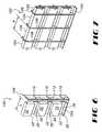
Figure 1 is a perspective illustration of a simplified antenna not constructed according to the present invention and using coaxial cables and parallel plate waveguides.Figure 2 is an exploded view of a part of a second antenna according to the present invention constructed using circuit cards In place of the coaxial cables ofFigure 1 .Figure 3 is a perspective illustration of the antenna shown in partial exploded view inFigure 2 .Figure 4 is an exploded view of a part of parallel plate waveguide and a pair of circuit cards for making a third antenna not constructed following the teachings of the present Invention.Figure 5 used a perspective illustration of the antenna shown in a partially exploded view inFigure 4 .Figure 6 is an exploded view of a part of a parallel plate waveguide and a pair of circuit cards for making a fourth antenna not constructed according to the teachings of the present invention.Figure 7 is a perspective illustration of the antenna shown in a partially exploded view inFigure 6 .Figure 8 is a perspective illustration of a fifth antenna not constructed following the teachings of the present invention.Figure 1 shows a phasedarray radar antenna 20. Theantenna 20 inFigure 1 has ametal structure 21 that forms three approximately horizontally extendingchannels Figure 1 thechannels 22a, b and c are positioned one on top of the other and extend from left to right in the Figure. Eachchannel 22 includes at least one wave launcher 24, and illustrated eachchannel 22 has threewave launchers channels 22 and wave launchers 24 therefore form a 3 x 3 array of parallel plate resonators.- Phased array antennas in general are constructed of identical wave launchers and cavities that are arranged in a predetermined (usually regular) array. In this application elements that are identical except for their location are given the same reference numerals with a letter suffixed. Similarly, to avoid unnecessary detail in many places this application describes in detail only one element or combination of elements. The other elements that differ only in position are identical to those described, as would be readily understood by those skilled in the art.
- Each
channel 22 has aback wall 26 and atop wall 28 andbottom wall 30 that form the channel. Thewalls bottom walls back wall 26 is perpendicular to them. Thechannels 22 are joined byconductive face plates 32 that position the channels parallel to each other. Thus, the cavity formed by eachchannel 22 has an open front and open lateral ends. Thechannels 22 andface plates 32 may conveniently be made of metal by conventional machining and manufacturing processes. - Each
channel 22 includes a at least one monopole wave launcher 24. In the embodiment ofFigure 1 , the wave launchers 24 are coaxial cables, three in each channel. Theouter shielding 34 of each coaxial cable is secured and electrically connected to thechannel 22, and the inner cable conductor 36 extends into the cavity defined by the top, back, andbottom walls bottom walls back wall 26. - The proportions of the
walls distance 38 from the open front edge to the back wall is about 1/8 (one eighth) of the wave length of the signal for which the antenna is tuned. Together thetop wall 28,back wall 26,bottom wall 30, and each monopole wave launcher 24 form a resonator. - An antenna made like that shown in
Figure 1 is expected to perform quite well. Not only is it relatively low profile, being only 1/8 wavelength deep, but it has a bandwidth of over 50%. However, the cost of manufacture would be quite high because of the need to attach the outercoaxial cables 34 to thechannels 22 carefully in a very small space. - The antennas described bellow demonstrate various other ways to build an antenna that uses the teachings of the present invention, and that may prove easier to execute than that shown in
Figure 1 . These antennas, like that shown inFigure 1 , are shown in small arrays, but it is readily apparent that the antennas described herein may be made to any desired size. In the following description the reference numerals used in connection withFigure 1 are repeated for corresponding elements in the remaining antennas, where those elements have the same function and substantially identical structure. Where the structures vary significantly, they are assigned new reference numerals.Figures 2 and 3 illustrate asecond antenna 50 that uses the precepts of the present invention. Here the wave launchers 24 are formed oncircuit card assemblies - Each circuit card assembly 52 (
Figure 2 ) is formed of twocards conductive strip lines Figure 1 . Specifically, thecard 68 has astrip line 70 on thesurface facing card 66, and the outside surfaces of thecards conductive material 72 on that part of the respective card that surrounds thestrip line 70. Only theconductive material 72 on the outside surface ofcard 66 is shown. However, a mirror image of the material is also present on the outside surface of thecard 68. Note that theconductive material 72 extends only part way down thetabs 54, stopping just where the tab extends through theopening 58. In this way thecentral strip line 70 can act as the center conductor of a coaxial cable. The twocards Figure 2 , are laminated to each other as shown inFigure 3 to form acircuit card assembly 52. Eachcircuit card assembly 52 has a series oftabs 54, each tab extending out from thefront edge 56 of the card and then downward. Thetabs 54 fit throughopenings 58 in themetal structure 60 so that they can extend into thechannels 22 at the desired locations. - The
antenna 50 ofFigure 3 is assembled from threecircuit card assemblies 52 and ametal structure 60 similar to that shown inFigure 1 . The metal structure has threechannels 22a, b and c extending from left to right in the Figures. Thetop walls 28 of the channels are made withopenings 58 or holes that fit thetabs 54 of the circuit card assemblies. Eachcircuit card assembly 52 is inserted into theopenings 58 in themetal structure 60. Solder connections are made between thecard assemblies 52 and themetal structure 60 as required. When assembled, themetal structure 60 andcircuit card assemblies 52 form resonators, as shown inFigure 3 , a 3 x 3 array of resonators. - The
circuit card assemblies 52 may be provided with appropriate connectors for electrical connection to the RF electronics that drive the antenna. Alternatively, the RF electronics may be directly attached to the circuit cards. Figures 4 and 5 illustrate anotherantenna 80. Here thecircuit card assemblies 82 are rectangular in overall shape. The strip lines 84 on the card assemblies have the same shape as in the antenna illustrated inFigures 2 and 3 , but no tab is formed. Instead aslot 86 for each card assembly is cut down the back of themetal structure 88, with the slots being just wide enough to receive thecard assemblies 82. Thecard assemblies 82 have plated throughholes 90 that match the shape of theback wall 26 andbottom wall 30, and front faces 32 of the resonators. The plated throughholes 90 are spaced so that they reflect radiation of the frequency band for which the antenna Is to be used. Again thecard assemblies 82 may or may not include RF electronics.Figures 6 and 7 illustrate anotherantenna 100. Here themetal structure 102 has been divided intoseparate columns 104. Thecircuit card assemblies 106 have a series of plated through holes 108 that align with thefaceplate 32,back wall 26, andbottom wall 30 of eachresonator cavity 22. As before, thestrip lines circuit card assemblies 106 form wave launchers. Theantenna 100 is assembled by forming a sandwich with alternatingcircuit card assemblies 106 andmetal columns 104.Figure 8 illustrates analternative antenna 120. Theantenna 120 has fourrows wave launchers 124 with four resonator cavities in each row 126a, 126b, 126c, 126d (only the resonators inrow 122d are labeled). In addition, the back walls are not flat across their entire width as in the previously described antennas. Instead, the rear walls around eachwave launcher 124 have aflat surface 128 and two oppositelyinclined surfaces wedges Figures 1-7 , thewave launchers 124 in theantenna 120 are staggered. Accordingly, thewave launchers 124 Inrows rows - In any of the
antennas resonator cavity 124 in the case of antenna 120) may be reduced by filling the channel with a low loss dielectric material. Suitable materials include polystyrene, polyethylene and polytetrafluorethyfene. Use of such a filler allows the antenna to be made shallower. This makes it better suited for applications such as aircraft or missiles where space is at a premium. The dielectric material may also cover the entire antenna array, allowing it to function as a radome. Further, to accommodate mounting on curved surfaces, an antenna constructed according to the teachings of the present invention need not be flat; the antenna may be curved in one or two planes.
Claims (6)
- A low-profile, phased array antenna (50) comprising a plurality of parallel plate waveguides, and a plurality of wave launchers (52, 82, 106, 124)
wherein each of the waveguides has an open front and open ends;
wherein the plurality of wave launchers (52, 82, 106, 124) are regularly arranged in a two-dimensional array with each wave launcher (52, 82, 106, 124) being positioned in one of the parallel plate waveguides;characterised in that
each wave launcher (52, 82, 106, 124) is formed by a strip line (70, 110) on an inner surface of a first circuit card (66) and a shielding for the wave launcher is formed by a conductive material on outer surfaces of the first circuit card (66) and a second circuit card (68), whereby the strip line (70, 110) and the conductive material on the first and second circuit cards (66, 68) form the electric equivalent of coaxial cables,
the waveguides include an opening (58) for each wave launcher (52) positioned therein,
the circuit cards (66, 68) include a tab (54) for each wave launcher (52) with the respective strip line (70) positioned on the tab (54), and
each tab (54) extends from a front edge (56) of the circuit cards (66, 68) and then parallel to a rear wall of the waveguide, through one of the openings (58) in the waveguides to position the strip lines (70), and thus the wave launchers, within the waveguides. - The antenna as set forth in the preceding claim, comprising a plurality of first and second circuit cards (66, 68) forming the plurality of wave launchers (52, 82, 106, 124).
- The antenna of the preceding claims, wherein each of the first circuit cards (66) includes more than one strip line (70, 110) forming more than one of the plurality of the wave launchers (52, 82, 106,124).
- The antenna of either of the two preceding claims, wherein each strip line (70, 110) has a portion parallel to a rear wall of the waveguide, whereby the wave launcher (52, 82, 106, 124) has at least one linear element parallel to the rear wall.
- The antenna of the preceding claim, wherein the distance between the opening and the rear wall is approximately 1/8 of the wavelength of the signal to be transmitted or received.
- The antenna of any of the preceding claims, wherein each of the wave guides is filled with a low-loss dielectric material.
Applications Claiming Priority (3)
| Application Number | Priority Date | Filing Date | Title |
|---|---|---|---|
| US10/255,313US6864851B2 (en) | 2002-09-26 | 2002-09-26 | Low profile wideband antenna array |
| US255313 | 2002-09-26 | ||
| PCT/US2003/029207WO2004030151A1 (en) | 2002-09-26 | 2003-09-19 | Low profile wideband antenna array |
Publications (2)
| Publication Number | Publication Date |
|---|---|
| EP1547201A1 EP1547201A1 (en) | 2005-06-29 |
| EP1547201B1true EP1547201B1 (en) | 2008-07-30 |
Family
ID=32029091
Family Applications (1)
| Application Number | Title | Priority Date | Filing Date |
|---|---|---|---|
| EP03759277AExpired - LifetimeEP1547201B1 (en) | 2002-09-26 | 2003-09-19 | Low profile wideband antenna array |
Country Status (7)
| Country | Link |
|---|---|
| US (1) | US6864851B2 (en) |
| EP (1) | EP1547201B1 (en) |
| AT (1) | ATE403246T1 (en) |
| AU (1) | AU2003275007A1 (en) |
| DE (1) | DE60322554D1 (en) |
| IL (1) | IL166916A (en) |
| WO (1) | WO2004030151A1 (en) |
Families Citing this family (147)
| Publication number | Priority date | Publication date | Assignee | Title |
|---|---|---|---|---|
| US7098853B2 (en)* | 2004-07-21 | 2006-08-29 | Raytheon Company | Conformal channel monopole array antenna |
| US7352338B2 (en)* | 2004-07-21 | 2008-04-01 | Motorola, Inc. | Wideband antenna with reduced dielectric loss |
| US8169378B2 (en)* | 2008-02-08 | 2012-05-01 | Raytheon Company | System and method for stabilizing an electronic array |
| US9113347B2 (en) | 2012-12-05 | 2015-08-18 | At&T Intellectual Property I, Lp | Backhaul link for distributed antenna system |
| US10009065B2 (en) | 2012-12-05 | 2018-06-26 | At&T Intellectual Property I, L.P. | Backhaul link for distributed antenna system |
| US9999038B2 (en) | 2013-05-31 | 2018-06-12 | At&T Intellectual Property I, L.P. | Remote distributed antenna system |
| US9525524B2 (en) | 2013-05-31 | 2016-12-20 | At&T Intellectual Property I, L.P. | Remote distributed antenna system |
| US8897697B1 (en) | 2013-11-06 | 2014-11-25 | At&T Intellectual Property I, Lp | Millimeter-wave surface-wave communications |
| US9692101B2 (en) | 2014-08-26 | 2017-06-27 | At&T Intellectual Property I, L.P. | Guided wave couplers for coupling electromagnetic waves between a waveguide surface and a surface of a wire |
| US9768833B2 (en) | 2014-09-15 | 2017-09-19 | At&T Intellectual Property I, L.P. | Method and apparatus for sensing a condition in a transmission medium of electromagnetic waves |
| US10063280B2 (en) | 2014-09-17 | 2018-08-28 | At&T Intellectual Property I, L.P. | Monitoring and mitigating conditions in a communication network |
| US9615269B2 (en) | 2014-10-02 | 2017-04-04 | At&T Intellectual Property I, L.P. | Method and apparatus that provides fault tolerance in a communication network |
| US9685992B2 (en) | 2014-10-03 | 2017-06-20 | At&T Intellectual Property I, L.P. | Circuit panel network and methods thereof |
| US9503189B2 (en) | 2014-10-10 | 2016-11-22 | At&T Intellectual Property I, L.P. | Method and apparatus for arranging communication sessions in a communication system |
| US9973299B2 (en) | 2014-10-14 | 2018-05-15 | At&T Intellectual Property I, L.P. | Method and apparatus for adjusting a mode of communication in a communication network |
| US9762289B2 (en) | 2014-10-14 | 2017-09-12 | At&T Intellectual Property I, L.P. | Method and apparatus for transmitting or receiving signals in a transportation system |
| US9520945B2 (en) | 2014-10-21 | 2016-12-13 | At&T Intellectual Property I, L.P. | Apparatus for providing communication services and methods thereof |
| US9312919B1 (en) | 2014-10-21 | 2016-04-12 | At&T Intellectual Property I, Lp | Transmission device with impairment compensation and methods for use therewith |
| US9780834B2 (en) | 2014-10-21 | 2017-10-03 | At&T Intellectual Property I, L.P. | Method and apparatus for transmitting electromagnetic waves |
| US9577306B2 (en) | 2014-10-21 | 2017-02-21 | At&T Intellectual Property I, L.P. | Guided-wave transmission device and methods for use therewith |
| US9653770B2 (en) | 2014-10-21 | 2017-05-16 | At&T Intellectual Property I, L.P. | Guided wave coupler, coupling module and methods for use therewith |
| US9627768B2 (en) | 2014-10-21 | 2017-04-18 | At&T Intellectual Property I, L.P. | Guided-wave transmission device with non-fundamental mode propagation and methods for use therewith |
| US9769020B2 (en) | 2014-10-21 | 2017-09-19 | At&T Intellectual Property I, L.P. | Method and apparatus for responding to events affecting communications in a communication network |
| US9997819B2 (en) | 2015-06-09 | 2018-06-12 | At&T Intellectual Property I, L.P. | Transmission medium and method for facilitating propagation of electromagnetic waves via a core |
| US9544006B2 (en) | 2014-11-20 | 2017-01-10 | At&T Intellectual Property I, L.P. | Transmission device with mode division multiplexing and methods for use therewith |
| US10009067B2 (en) | 2014-12-04 | 2018-06-26 | At&T Intellectual Property I, L.P. | Method and apparatus for configuring a communication interface |
| US10243784B2 (en) | 2014-11-20 | 2019-03-26 | At&T Intellectual Property I, L.P. | System for generating topology information and methods thereof |
| US9954287B2 (en) | 2014-11-20 | 2018-04-24 | At&T Intellectual Property I, L.P. | Apparatus for converting wireless signals and electromagnetic waves and methods thereof |
| US9461706B1 (en) | 2015-07-31 | 2016-10-04 | At&T Intellectual Property I, Lp | Method and apparatus for exchanging communication signals |
| US9742462B2 (en) | 2014-12-04 | 2017-08-22 | At&T Intellectual Property I, L.P. | Transmission medium and communication interfaces and methods for use therewith |
| US10340573B2 (en) | 2016-10-26 | 2019-07-02 | At&T Intellectual Property I, L.P. | Launcher with cylindrical coupling device and methods for use therewith |
| US9800327B2 (en) | 2014-11-20 | 2017-10-24 | At&T Intellectual Property I, L.P. | Apparatus for controlling operations of a communication device and methods thereof |
| US10144036B2 (en) | 2015-01-30 | 2018-12-04 | At&T Intellectual Property I, L.P. | Method and apparatus for mitigating interference affecting a propagation of electromagnetic waves guided by a transmission medium |
| US9876570B2 (en) | 2015-02-20 | 2018-01-23 | At&T Intellectual Property I, Lp | Guided-wave transmission device with non-fundamental mode propagation and methods for use therewith |
| US9749013B2 (en) | 2015-03-17 | 2017-08-29 | At&T Intellectual Property I, L.P. | Method and apparatus for reducing attenuation of electromagnetic waves guided by a transmission medium |
| US10224981B2 (en) | 2015-04-24 | 2019-03-05 | At&T Intellectual Property I, Lp | Passive electrical coupling device and methods for use therewith |
| US9705561B2 (en) | 2015-04-24 | 2017-07-11 | At&T Intellectual Property I, L.P. | Directional coupling device and methods for use therewith |
| US9948354B2 (en) | 2015-04-28 | 2018-04-17 | At&T Intellectual Property I, L.P. | Magnetic coupling device with reflective plate and methods for use therewith |
| US9793954B2 (en) | 2015-04-28 | 2017-10-17 | At&T Intellectual Property I, L.P. | Magnetic coupling device and methods for use therewith |
| US9871282B2 (en) | 2015-05-14 | 2018-01-16 | At&T Intellectual Property I, L.P. | At least one transmission medium having a dielectric surface that is covered at least in part by a second dielectric |
| US9490869B1 (en) | 2015-05-14 | 2016-11-08 | At&T Intellectual Property I, L.P. | Transmission medium having multiple cores and methods for use therewith |
| US9748626B2 (en) | 2015-05-14 | 2017-08-29 | At&T Intellectual Property I, L.P. | Plurality of cables having different cross-sectional shapes which are bundled together to form a transmission medium |
| US10650940B2 (en) | 2015-05-15 | 2020-05-12 | At&T Intellectual Property I, L.P. | Transmission medium having a conductive material and methods for use therewith |
| US9917341B2 (en) | 2015-05-27 | 2018-03-13 | At&T Intellectual Property I, L.P. | Apparatus and method for launching electromagnetic waves and for modifying radial dimensions of the propagating electromagnetic waves |
| US9912381B2 (en) | 2015-06-03 | 2018-03-06 | At&T Intellectual Property I, Lp | Network termination and methods for use therewith |
| US10812174B2 (en) | 2015-06-03 | 2020-10-20 | At&T Intellectual Property I, L.P. | Client node device and methods for use therewith |
| US9866309B2 (en) | 2015-06-03 | 2018-01-09 | At&T Intellectual Property I, Lp | Host node device and methods for use therewith |
| US10103801B2 (en) | 2015-06-03 | 2018-10-16 | At&T Intellectual Property I, L.P. | Host node device and methods for use therewith |
| US9913139B2 (en) | 2015-06-09 | 2018-03-06 | At&T Intellectual Property I, L.P. | Signal fingerprinting for authentication of communicating devices |
| US9608692B2 (en) | 2015-06-11 | 2017-03-28 | At&T Intellectual Property I, L.P. | Repeater and methods for use therewith |
| US10142086B2 (en) | 2015-06-11 | 2018-11-27 | At&T Intellectual Property I, L.P. | Repeater and methods for use therewith |
| US9820146B2 (en) | 2015-06-12 | 2017-11-14 | At&T Intellectual Property I, L.P. | Method and apparatus for authentication and identity management of communicating devices |
| US9667317B2 (en) | 2015-06-15 | 2017-05-30 | At&T Intellectual Property I, L.P. | Method and apparatus for providing security using network traffic adjustments |
| US9509415B1 (en) | 2015-06-25 | 2016-11-29 | At&T Intellectual Property I, L.P. | Methods and apparatus for inducing a fundamental wave mode on a transmission medium |
| US9865911B2 (en) | 2015-06-25 | 2018-01-09 | At&T Intellectual Property I, L.P. | Waveguide system for slot radiating first electromagnetic waves that are combined into a non-fundamental wave mode second electromagnetic wave on a transmission medium |
| US9640850B2 (en) | 2015-06-25 | 2017-05-02 | At&T Intellectual Property I, L.P. | Methods and apparatus for inducing a non-fundamental wave mode on a transmission medium |
| US9628116B2 (en) | 2015-07-14 | 2017-04-18 | At&T Intellectual Property I, L.P. | Apparatus and methods for transmitting wireless signals |
| US9853342B2 (en) | 2015-07-14 | 2017-12-26 | At&T Intellectual Property I, L.P. | Dielectric transmission medium connector and methods for use therewith |
| US10341142B2 (en) | 2015-07-14 | 2019-07-02 | At&T Intellectual Property I, L.P. | Apparatus and methods for generating non-interfering electromagnetic waves on an uninsulated conductor |
| US10320586B2 (en) | 2015-07-14 | 2019-06-11 | At&T Intellectual Property I, L.P. | Apparatus and methods for generating non-interfering electromagnetic waves on an insulated transmission medium |
| US10205655B2 (en) | 2015-07-14 | 2019-02-12 | At&T Intellectual Property I, L.P. | Apparatus and methods for communicating utilizing an antenna array and multiple communication paths |
| US10033108B2 (en) | 2015-07-14 | 2018-07-24 | At&T Intellectual Property I, L.P. | Apparatus and methods for generating an electromagnetic wave having a wave mode that mitigates interference |
| US9722318B2 (en) | 2015-07-14 | 2017-08-01 | At&T Intellectual Property I, L.P. | Method and apparatus for coupling an antenna to a device |
| US10033107B2 (en) | 2015-07-14 | 2018-07-24 | At&T Intellectual Property I, L.P. | Method and apparatus for coupling an antenna to a device |
| US10170840B2 (en) | 2015-07-14 | 2019-01-01 | At&T Intellectual Property I, L.P. | Apparatus and methods for sending or receiving electromagnetic signals |
| US10044409B2 (en) | 2015-07-14 | 2018-08-07 | At&T Intellectual Property I, L.P. | Transmission medium and methods for use therewith |
| US9882257B2 (en) | 2015-07-14 | 2018-01-30 | At&T Intellectual Property I, L.P. | Method and apparatus for launching a wave mode that mitigates interference |
| US9847566B2 (en) | 2015-07-14 | 2017-12-19 | At&T Intellectual Property I, L.P. | Method and apparatus for adjusting a field of a signal to mitigate interference |
| US10148016B2 (en) | 2015-07-14 | 2018-12-04 | At&T Intellectual Property I, L.P. | Apparatus and methods for communicating utilizing an antenna array |
| US9793951B2 (en) | 2015-07-15 | 2017-10-17 | At&T Intellectual Property I, L.P. | Method and apparatus for launching a wave mode that mitigates interference |
| US9608740B2 (en) | 2015-07-15 | 2017-03-28 | At&T Intellectual Property I, L.P. | Method and apparatus for launching a wave mode that mitigates interference |
| US10090606B2 (en) | 2015-07-15 | 2018-10-02 | At&T Intellectual Property I, L.P. | Antenna system with dielectric array and methods for use therewith |
| US9749053B2 (en) | 2015-07-23 | 2017-08-29 | At&T Intellectual Property I, L.P. | Node device, repeater and methods for use therewith |
| US9871283B2 (en) | 2015-07-23 | 2018-01-16 | At&T Intellectual Property I, Lp | Transmission medium having a dielectric core comprised of plural members connected by a ball and socket configuration |
| US9948333B2 (en) | 2015-07-23 | 2018-04-17 | At&T Intellectual Property I, L.P. | Method and apparatus for wireless communications to mitigate interference |
| US9912027B2 (en) | 2015-07-23 | 2018-03-06 | At&T Intellectual Property I, L.P. | Method and apparatus for exchanging communication signals |
| US9967173B2 (en) | 2015-07-31 | 2018-05-08 | At&T Intellectual Property I, L.P. | Method and apparatus for authentication and identity management of communicating devices |
| US9735833B2 (en) | 2015-07-31 | 2017-08-15 | At&T Intellectual Property I, L.P. | Method and apparatus for communications management in a neighborhood network |
| US9904535B2 (en) | 2015-09-14 | 2018-02-27 | At&T Intellectual Property I, L.P. | Method and apparatus for distributing software |
| US10079661B2 (en) | 2015-09-16 | 2018-09-18 | At&T Intellectual Property I, L.P. | Method and apparatus for use with a radio distributed antenna system having a clock reference |
| US10009063B2 (en) | 2015-09-16 | 2018-06-26 | At&T Intellectual Property I, L.P. | Method and apparatus for use with a radio distributed antenna system having an out-of-band reference signal |
| US10136434B2 (en) | 2015-09-16 | 2018-11-20 | At&T Intellectual Property I, L.P. | Method and apparatus for use with a radio distributed antenna system having an ultra-wideband control channel |
| US9769128B2 (en) | 2015-09-28 | 2017-09-19 | At&T Intellectual Property I, L.P. | Method and apparatus for encryption of communications over a network |
| US9729197B2 (en) | 2015-10-01 | 2017-08-08 | At&T Intellectual Property I, L.P. | Method and apparatus for communicating network management traffic over a network |
| US9876264B2 (en) | 2015-10-02 | 2018-01-23 | At&T Intellectual Property I, Lp | Communication system, guided wave switch and methods for use therewith |
| US10355367B2 (en) | 2015-10-16 | 2019-07-16 | At&T Intellectual Property I, L.P. | Antenna structure for exchanging wireless signals |
| US10665942B2 (en) | 2015-10-16 | 2020-05-26 | At&T Intellectual Property I, L.P. | Method and apparatus for adjusting wireless communications |
| US9912419B1 (en) | 2016-08-24 | 2018-03-06 | At&T Intellectual Property I, L.P. | Method and apparatus for managing a fault in a distributed antenna system |
| US9860075B1 (en) | 2016-08-26 | 2018-01-02 | At&T Intellectual Property I, L.P. | Method and communication node for broadband distribution |
| US10291311B2 (en) | 2016-09-09 | 2019-05-14 | At&T Intellectual Property I, L.P. | Method and apparatus for mitigating a fault in a distributed antenna system |
| US11032819B2 (en) | 2016-09-15 | 2021-06-08 | At&T Intellectual Property I, L.P. | Method and apparatus for use with a radio distributed antenna system having a control channel reference signal |
| US10135147B2 (en) | 2016-10-18 | 2018-11-20 | At&T Intellectual Property I, L.P. | Apparatus and methods for launching guided waves via an antenna |
| US10340600B2 (en) | 2016-10-18 | 2019-07-02 | At&T Intellectual Property I, L.P. | Apparatus and methods for launching guided waves via plural waveguide systems |
| US10135146B2 (en) | 2016-10-18 | 2018-11-20 | At&T Intellectual Property I, L.P. | Apparatus and methods for launching guided waves via circuits |
| US10374316B2 (en) | 2016-10-21 | 2019-08-06 | At&T Intellectual Property I, L.P. | System and dielectric antenna with non-uniform dielectric |
| US10811767B2 (en) | 2016-10-21 | 2020-10-20 | At&T Intellectual Property I, L.P. | System and dielectric antenna with convex dielectric radome |
| US9991580B2 (en) | 2016-10-21 | 2018-06-05 | At&T Intellectual Property I, L.P. | Launcher and coupling system for guided wave mode cancellation |
| US9876605B1 (en) | 2016-10-21 | 2018-01-23 | At&T Intellectual Property I, L.P. | Launcher and coupling system to support desired guided wave mode |
| US10312567B2 (en) | 2016-10-26 | 2019-06-04 | At&T Intellectual Property I, L.P. | Launcher with planar strip antenna and methods for use therewith |
| US10498044B2 (en) | 2016-11-03 | 2019-12-03 | At&T Intellectual Property I, L.P. | Apparatus for configuring a surface of an antenna |
| US10224634B2 (en) | 2016-11-03 | 2019-03-05 | At&T Intellectual Property I, L.P. | Methods and apparatus for adjusting an operational characteristic of an antenna |
| US10291334B2 (en) | 2016-11-03 | 2019-05-14 | At&T Intellectual Property I, L.P. | System for detecting a fault in a communication system |
| US10225025B2 (en) | 2016-11-03 | 2019-03-05 | At&T Intellectual Property I, L.P. | Method and apparatus for detecting a fault in a communication system |
| US10535928B2 (en) | 2016-11-23 | 2020-01-14 | At&T Intellectual Property I, L.P. | Antenna system and methods for use therewith |
| US10340603B2 (en) | 2016-11-23 | 2019-07-02 | At&T Intellectual Property I, L.P. | Antenna system having shielded structural configurations for assembly |
| US10340601B2 (en) | 2016-11-23 | 2019-07-02 | At&T Intellectual Property I, L.P. | Multi-antenna system and methods for use therewith |
| US10090594B2 (en) | 2016-11-23 | 2018-10-02 | At&T Intellectual Property I, L.P. | Antenna system having structural configurations for assembly |
| US10178445B2 (en) | 2016-11-23 | 2019-01-08 | At&T Intellectual Property I, L.P. | Methods, devices, and systems for load balancing between a plurality of waveguides |
| US10361489B2 (en) | 2016-12-01 | 2019-07-23 | At&T Intellectual Property I, L.P. | Dielectric dish antenna system and methods for use therewith |
| US10305190B2 (en) | 2016-12-01 | 2019-05-28 | At&T Intellectual Property I, L.P. | Reflecting dielectric antenna system and methods for use therewith |
| US10819035B2 (en) | 2016-12-06 | 2020-10-27 | At&T Intellectual Property I, L.P. | Launcher with helical antenna and methods for use therewith |
| US9927517B1 (en) | 2016-12-06 | 2018-03-27 | At&T Intellectual Property I, L.P. | Apparatus and methods for sensing rainfall |
| US10135145B2 (en) | 2016-12-06 | 2018-11-20 | At&T Intellectual Property I, L.P. | Apparatus and methods for generating an electromagnetic wave along a transmission medium |
| US10020844B2 (en) | 2016-12-06 | 2018-07-10 | T&T Intellectual Property I, L.P. | Method and apparatus for broadcast communication via guided waves |
| US10694379B2 (en) | 2016-12-06 | 2020-06-23 | At&T Intellectual Property I, L.P. | Waveguide system with device-based authentication and methods for use therewith |
| US10755542B2 (en) | 2016-12-06 | 2020-08-25 | At&T Intellectual Property I, L.P. | Method and apparatus for surveillance via guided wave communication |
| US10439675B2 (en) | 2016-12-06 | 2019-10-08 | At&T Intellectual Property I, L.P. | Method and apparatus for repeating guided wave communication signals |
| US10727599B2 (en) | 2016-12-06 | 2020-07-28 | At&T Intellectual Property I, L.P. | Launcher with slot antenna and methods for use therewith |
| US10326494B2 (en) | 2016-12-06 | 2019-06-18 | At&T Intellectual Property I, L.P. | Apparatus for measurement de-embedding and methods for use therewith |
| US10637149B2 (en) | 2016-12-06 | 2020-04-28 | At&T Intellectual Property I, L.P. | Injection molded dielectric antenna and methods for use therewith |
| US10382976B2 (en) | 2016-12-06 | 2019-08-13 | At&T Intellectual Property I, L.P. | Method and apparatus for managing wireless communications based on communication paths and network device positions |
| US10446936B2 (en) | 2016-12-07 | 2019-10-15 | At&T Intellectual Property I, L.P. | Multi-feed dielectric antenna system and methods for use therewith |
| US10389029B2 (en) | 2016-12-07 | 2019-08-20 | At&T Intellectual Property I, L.P. | Multi-feed dielectric antenna system with core selection and methods for use therewith |
| US10243270B2 (en) | 2016-12-07 | 2019-03-26 | At&T Intellectual Property I, L.P. | Beam adaptive multi-feed dielectric antenna system and methods for use therewith |
| US10139820B2 (en) | 2016-12-07 | 2018-11-27 | At&T Intellectual Property I, L.P. | Method and apparatus for deploying equipment of a communication system |
| US10359749B2 (en) | 2016-12-07 | 2019-07-23 | At&T Intellectual Property I, L.P. | Method and apparatus for utilities management via guided wave communication |
| US10027397B2 (en) | 2016-12-07 | 2018-07-17 | At&T Intellectual Property I, L.P. | Distributed antenna system and methods for use therewith |
| US10547348B2 (en) | 2016-12-07 | 2020-01-28 | At&T Intellectual Property I, L.P. | Method and apparatus for switching transmission mediums in a communication system |
| US9893795B1 (en) | 2016-12-07 | 2018-02-13 | At&T Intellectual Property I, Lp | Method and repeater for broadband distribution |
| US10168695B2 (en) | 2016-12-07 | 2019-01-01 | At&T Intellectual Property I, L.P. | Method and apparatus for controlling an unmanned aircraft |
| US10069535B2 (en) | 2016-12-08 | 2018-09-04 | At&T Intellectual Property I, L.P. | Apparatus and methods for launching electromagnetic waves having a certain electric field structure |
| US10530505B2 (en) | 2016-12-08 | 2020-01-07 | At&T Intellectual Property I, L.P. | Apparatus and methods for launching electromagnetic waves along a transmission medium |
| US10411356B2 (en) | 2016-12-08 | 2019-09-10 | At&T Intellectual Property I, L.P. | Apparatus and methods for selectively targeting communication devices with an antenna array |
| US10938108B2 (en) | 2016-12-08 | 2021-03-02 | At&T Intellectual Property I, L.P. | Frequency selective multi-feed dielectric antenna system and methods for use therewith |
| US10103422B2 (en) | 2016-12-08 | 2018-10-16 | At&T Intellectual Property I, L.P. | Method and apparatus for mounting network devices |
| US10326689B2 (en) | 2016-12-08 | 2019-06-18 | At&T Intellectual Property I, L.P. | Method and system for providing alternative communication paths |
| US10601494B2 (en) | 2016-12-08 | 2020-03-24 | At&T Intellectual Property I, L.P. | Dual-band communication device and method for use therewith |
| US10916969B2 (en) | 2016-12-08 | 2021-02-09 | At&T Intellectual Property I, L.P. | Method and apparatus for providing power using an inductive coupling |
| US9911020B1 (en) | 2016-12-08 | 2018-03-06 | At&T Intellectual Property I, L.P. | Method and apparatus for tracking via a radio frequency identification device |
| US10777873B2 (en) | 2016-12-08 | 2020-09-15 | At&T Intellectual Property I, L.P. | Method and apparatus for mounting network devices |
| US10389037B2 (en) | 2016-12-08 | 2019-08-20 | At&T Intellectual Property I, L.P. | Apparatus and methods for selecting sections of an antenna array and use therewith |
| US9998870B1 (en) | 2016-12-08 | 2018-06-12 | At&T Intellectual Property I, L.P. | Method and apparatus for proximity sensing |
| US10340983B2 (en) | 2016-12-09 | 2019-07-02 | At&T Intellectual Property I, L.P. | Method and apparatus for surveying remote sites via guided wave communications |
| US10264586B2 (en) | 2016-12-09 | 2019-04-16 | At&T Mobility Ii Llc | Cloud-based packet controller and methods for use therewith |
| US9838896B1 (en) | 2016-12-09 | 2017-12-05 | At&T Intellectual Property I, L.P. | Method and apparatus for assessing network coverage |
| US9973940B1 (en) | 2017-02-27 | 2018-05-15 | At&T Intellectual Property I, L.P. | Apparatus and methods for dynamic impedance matching of a guided wave launcher |
| US10298293B2 (en) | 2017-03-13 | 2019-05-21 | At&T Intellectual Property I, L.P. | Apparatus of communication utilizing wireless network devices |
Citations (1)
| Publication number | Priority date | Publication date | Assignee | Title |
|---|---|---|---|---|
| EP0249310A1 (en)* | 1986-06-10 | 1987-12-16 | Canadian Marconi Company | Waveguide to stripline transition |
Family Cites Families (7)
| Publication number | Priority date | Publication date | Assignee | Title |
|---|---|---|---|---|
| US2615132A (en)* | 1946-06-05 | 1952-10-21 | Victor H Rumsey | Directive broad band slot antenna system |
| US2817084A (en)* | 1953-08-05 | 1957-12-17 | Hughes Aircraft Co | Broadband antenna |
| US3453632A (en)* | 1966-10-06 | 1969-07-01 | Us Air Force | Single aperture multiple beam antennas |
| US3818490A (en)* | 1972-08-04 | 1974-06-18 | Westinghouse Electric Corp | Dual frequency array |
| GB2193379B (en)* | 1986-07-24 | 1990-04-18 | Gen Electric Plc | An antenna |
| US4862186A (en)* | 1986-11-12 | 1989-08-29 | Hughes Aircraft Company | Microwave antenna array waveguide assembly |
| US5579020A (en)* | 1993-09-27 | 1996-11-26 | Sensis Corporation | Lightweight edge-slotted waveguide antenna structure |
- 2002
- 2002-09-26USUS10/255,313patent/US6864851B2/ennot_activeExpired - Lifetime
- 2003
- 2003-09-19ATAT03759277Tpatent/ATE403246T1/ennot_activeIP Right Cessation
- 2003-09-19EPEP03759277Apatent/EP1547201B1/ennot_activeExpired - Lifetime
- 2003-09-19DEDE60322554Tpatent/DE60322554D1/ennot_activeExpired - Lifetime
- 2003-09-19AUAU2003275007Apatent/AU2003275007A1/ennot_activeAbandoned
- 2003-09-19WOPCT/US2003/029207patent/WO2004030151A1/ennot_activeApplication Discontinuation
- 2005
- 2005-02-15ILIL166916Apatent/IL166916A/enunknown
Patent Citations (1)
| Publication number | Priority date | Publication date | Assignee | Title |
|---|---|---|---|---|
| EP0249310A1 (en)* | 1986-06-10 | 1987-12-16 | Canadian Marconi Company | Waveguide to stripline transition |
Also Published As
| Publication number | Publication date |
|---|---|
| WO2004030151A1 (en) | 2004-04-08 |
| US20040061656A1 (en) | 2004-04-01 |
| US6864851B2 (en) | 2005-03-08 |
| IL166916A (en) | 2010-11-30 |
| DE60322554D1 (en) | 2008-09-11 |
| EP1547201A1 (en) | 2005-06-29 |
| ATE403246T1 (en) | 2008-08-15 |
| AU2003275007A1 (en) | 2004-04-19 |
Similar Documents
| Publication | Publication Date | Title |
|---|---|---|
| EP1547201B1 (en) | Low profile wideband antenna array | |
| US11837787B2 (en) | High frequency filter and phased array antenna comprising such a high frequency filter | |
| EP3888186B1 (en) | Ridge gap waveguide and multilayer antenna array including the same | |
| CN109314314B (en) | Array antenna | |
| EP3311449B1 (en) | Efficient planar phased array antenna assembly | |
| EP0985243B1 (en) | Microwave transmission device | |
| EP1398848B1 (en) | Laminated aperture antenna and multi-layered wiring board comprising the same | |
| CN108370100B (en) | Dual-polarized broadband radiator with single-plane strip line feed | |
| US7102581B1 (en) | Multiband waveguide reflector antenna feed | |
| EP2945222A1 (en) | A microwave or millimeter wave RF part using pin grid array (PGA) and/or ball grid array (BGA) technologies | |
| EP1856769B1 (en) | True-time-delay feed network for cts array | |
| EP1148583A1 (en) | Planar array antenna | |
| EP4097796B1 (en) | A scalable modular antenna arrangement | |
| EP2385583B1 (en) | Wideband cavity-backed slot antenna | |
| JP2001094340A (en) | Slot array antenna with cavity | |
| CN107768842B (en) | Antenna unit and array antenna for 5G mobile communication | |
| CN110957574B (en) | A stripline-fed broadband millimeter-wave antenna unit | |
| WO2021021017A1 (en) | A dipole antenna, an antenna array, and a method of fabricating the dipole antenna and the antenna array | |
| JP6474634B2 (en) | Planar array antenna | |
| EP3918664B1 (en) | Redirecting structure for electromagnetic waves | |
| US6781554B2 (en) | Compact wide scan periodically loaded edge slot waveguide array | |
| WO2024015132A1 (en) | Antenna filter units for base station antennas and related radio adaptor boards | |
| EP1389353B1 (en) | Transmission line | |
| JP3976004B2 (en) | T-branch waveguide and array antenna | |
| CN222601366U (en) | Millimeter wave radar antenna and radar apparatus |
Legal Events
| Date | Code | Title | Description |
|---|---|---|---|
| PUAI | Public reference made under article 153(3) epc to a published international application that has entered the european phase | Free format text:ORIGINAL CODE: 0009012 | |
| 17P | Request for examination filed | Effective date:20050421 | |
| AK | Designated contracting states | Kind code of ref document:A1 Designated state(s):AT BE BG CH CY CZ DE DK EE ES FI FR GB GR HU IE IT LI LU MC NL PT RO SE SI SK TR | |
| AX | Request for extension of the european patent | Extension state:AL LT LV MK | |
| DAX | Request for extension of the european patent (deleted) | ||
| GRAP | Despatch of communication of intention to grant a patent | Free format text:ORIGINAL CODE: EPIDOSNIGR1 | |
| GRAS | Grant fee paid | Free format text:ORIGINAL CODE: EPIDOSNIGR3 | |
| GRAA | (expected) grant | Free format text:ORIGINAL CODE: 0009210 | |
| AK | Designated contracting states | Kind code of ref document:B1 Designated state(s):AT BE BG CH CY CZ DE DK EE ES FI FR GB GR HU IE IT LI LU MC NL PT RO SE SI SK TR | |
| REG | Reference to a national code | Ref country code:GB Ref legal event code:FG4D | |
| REG | Reference to a national code | Ref country code:CH Ref legal event code:EP | |
| REF | Corresponds to: | Ref document number:60322554 Country of ref document:DE Date of ref document:20080911 Kind code of ref document:P | |
| REG | Reference to a national code | Ref country code:IE Ref legal event code:FG4D | |
| PG25 | Lapsed in a contracting state [announced via postgrant information from national office to epo] | Ref country code:NL Free format text:LAPSE BECAUSE OF FAILURE TO SUBMIT A TRANSLATION OF THE DESCRIPTION OR TO PAY THE FEE WITHIN THE PRESCRIBED TIME-LIMIT Effective date:20080730 Ref country code:ES Free format text:LAPSE BECAUSE OF FAILURE TO SUBMIT A TRANSLATION OF THE DESCRIPTION OR TO PAY THE FEE WITHIN THE PRESCRIBED TIME-LIMIT Effective date:20081110 Ref country code:PT Free format text:LAPSE BECAUSE OF FAILURE TO SUBMIT A TRANSLATION OF THE DESCRIPTION OR TO PAY THE FEE WITHIN THE PRESCRIBED TIME-LIMIT Effective date:20081230 | |
| PG25 | Lapsed in a contracting state [announced via postgrant information from national office to epo] | Ref country code:FI Free format text:LAPSE BECAUSE OF FAILURE TO SUBMIT A TRANSLATION OF THE DESCRIPTION OR TO PAY THE FEE WITHIN THE PRESCRIBED TIME-LIMIT Effective date:20080730 Ref country code:AT Free format text:LAPSE BECAUSE OF FAILURE TO SUBMIT A TRANSLATION OF THE DESCRIPTION OR TO PAY THE FEE WITHIN THE PRESCRIBED TIME-LIMIT Effective date:20080730 Ref country code:SI Free format text:LAPSE BECAUSE OF FAILURE TO SUBMIT A TRANSLATION OF THE DESCRIPTION OR TO PAY THE FEE WITHIN THE PRESCRIBED TIME-LIMIT Effective date:20080730 Ref country code:BG Free format text:LAPSE BECAUSE OF FAILURE TO SUBMIT A TRANSLATION OF THE DESCRIPTION OR TO PAY THE FEE WITHIN THE PRESCRIBED TIME-LIMIT Effective date:20081030 | |
| PG25 | Lapsed in a contracting state [announced via postgrant information from national office to epo] | Ref country code:BE Free format text:LAPSE BECAUSE OF FAILURE TO SUBMIT A TRANSLATION OF THE DESCRIPTION OR TO PAY THE FEE WITHIN THE PRESCRIBED TIME-LIMIT Effective date:20080730 | |
| PG25 | Lapsed in a contracting state [announced via postgrant information from national office to epo] | Ref country code:EE Free format text:LAPSE BECAUSE OF FAILURE TO SUBMIT A TRANSLATION OF THE DESCRIPTION OR TO PAY THE FEE WITHIN THE PRESCRIBED TIME-LIMIT Effective date:20080730 Ref country code:DK Free format text:LAPSE BECAUSE OF FAILURE TO SUBMIT A TRANSLATION OF THE DESCRIPTION OR TO PAY THE FEE WITHIN THE PRESCRIBED TIME-LIMIT Effective date:20080730 Ref country code:MC Free format text:LAPSE BECAUSE OF NON-PAYMENT OF DUE FEES Effective date:20080930 | |
| REG | Reference to a national code | Ref country code:CH Ref legal event code:PL | |
| PG25 | Lapsed in a contracting state [announced via postgrant information from national office to epo] | Ref country code:RO Free format text:LAPSE BECAUSE OF FAILURE TO SUBMIT A TRANSLATION OF THE DESCRIPTION OR TO PAY THE FEE WITHIN THE PRESCRIBED TIME-LIMIT Effective date:20080730 Ref country code:CZ Free format text:LAPSE BECAUSE OF FAILURE TO SUBMIT A TRANSLATION OF THE DESCRIPTION OR TO PAY THE FEE WITHIN THE PRESCRIBED TIME-LIMIT Effective date:20080730 Ref country code:SK Free format text:LAPSE BECAUSE OF FAILURE TO SUBMIT A TRANSLATION OF THE DESCRIPTION OR TO PAY THE FEE WITHIN THE PRESCRIBED TIME-LIMIT Effective date:20080730 | |
| PLBE | No opposition filed within time limit | Free format text:ORIGINAL CODE: 0009261 | |
| STAA | Information on the status of an ep patent application or granted ep patent | Free format text:STATUS: NO OPPOSITION FILED WITHIN TIME LIMIT | |
| 26N | No opposition filed | Effective date:20090506 | |
| PG25 | Lapsed in a contracting state [announced via postgrant information from national office to epo] | Ref country code:IE Free format text:LAPSE BECAUSE OF NON-PAYMENT OF DUE FEES Effective date:20080919 | |
| PG25 | Lapsed in a contracting state [announced via postgrant information from national office to epo] | Ref country code:IT Free format text:LAPSE BECAUSE OF FAILURE TO SUBMIT A TRANSLATION OF THE DESCRIPTION OR TO PAY THE FEE WITHIN THE PRESCRIBED TIME-LIMIT Effective date:20080730 | |
| PG25 | Lapsed in a contracting state [announced via postgrant information from national office to epo] | Ref country code:LI Free format text:LAPSE BECAUSE OF NON-PAYMENT OF DUE FEES Effective date:20080930 Ref country code:CH Free format text:LAPSE BECAUSE OF NON-PAYMENT OF DUE FEES Effective date:20080930 | |
| PG25 | Lapsed in a contracting state [announced via postgrant information from national office to epo] | Ref country code:SE Free format text:LAPSE BECAUSE OF FAILURE TO SUBMIT A TRANSLATION OF THE DESCRIPTION OR TO PAY THE FEE WITHIN THE PRESCRIBED TIME-LIMIT Effective date:20081030 | |
| PG25 | Lapsed in a contracting state [announced via postgrant information from national office to epo] | Ref country code:CY Free format text:LAPSE BECAUSE OF FAILURE TO SUBMIT A TRANSLATION OF THE DESCRIPTION OR TO PAY THE FEE WITHIN THE PRESCRIBED TIME-LIMIT Effective date:20080730 Ref country code:LU Free format text:LAPSE BECAUSE OF NON-PAYMENT OF DUE FEES Effective date:20080919 Ref country code:HU Free format text:LAPSE BECAUSE OF FAILURE TO SUBMIT A TRANSLATION OF THE DESCRIPTION OR TO PAY THE FEE WITHIN THE PRESCRIBED TIME-LIMIT Effective date:20090131 | |
| PG25 | Lapsed in a contracting state [announced via postgrant information from national office to epo] | Ref country code:TR Free format text:LAPSE BECAUSE OF FAILURE TO SUBMIT A TRANSLATION OF THE DESCRIPTION OR TO PAY THE FEE WITHIN THE PRESCRIBED TIME-LIMIT Effective date:20080730 | |
| PG25 | Lapsed in a contracting state [announced via postgrant information from national office to epo] | Ref country code:GR Free format text:LAPSE BECAUSE OF FAILURE TO SUBMIT A TRANSLATION OF THE DESCRIPTION OR TO PAY THE FEE WITHIN THE PRESCRIBED TIME-LIMIT Effective date:20081031 | |
| REG | Reference to a national code | Ref country code:FR Ref legal event code:PLFP Year of fee payment:14 | |
| REG | Reference to a national code | Ref country code:FR Ref legal event code:PLFP Year of fee payment:15 | |
| REG | Reference to a national code | Ref country code:FR Ref legal event code:PLFP Year of fee payment:16 | |
| PGFP | Annual fee paid to national office [announced via postgrant information from national office to epo] | Ref country code:DE Payment date:20180904 Year of fee payment:16 Ref country code:FR Payment date:20180813 Year of fee payment:16 | |
| PGFP | Annual fee paid to national office [announced via postgrant information from national office to epo] | Ref country code:GB Payment date:20180919 Year of fee payment:16 | |
| REG | Reference to a national code | Ref country code:DE Ref legal event code:R119 Ref document number:60322554 Country of ref document:DE | |
| PG25 | Lapsed in a contracting state [announced via postgrant information from national office to epo] | Ref country code:DE Free format text:LAPSE BECAUSE OF NON-PAYMENT OF DUE FEES Effective date:20200401 | |
| GBPC | Gb: european patent ceased through non-payment of renewal fee | Effective date:20190919 | |
| PG25 | Lapsed in a contracting state [announced via postgrant information from national office to epo] | Ref country code:FR Free format text:LAPSE BECAUSE OF NON-PAYMENT OF DUE FEES Effective date:20190930 Ref country code:GB Free format text:LAPSE BECAUSE OF NON-PAYMENT OF DUE FEES Effective date:20190919 |