EP1542056A2 - Optical shutter for plasma display panel and driving method thereof - Google Patents
Optical shutter for plasma display panel and driving method thereofDownload PDFInfo
- Publication number
- EP1542056A2 EP1542056A2EP04028863AEP04028863AEP1542056A2EP 1542056 A2EP1542056 A2EP 1542056A2EP 04028863 AEP04028863 AEP 04028863AEP 04028863 AEP04028863 AEP 04028863AEP 1542056 A2EP1542056 A2EP 1542056A2
- Authority
- EP
- European Patent Office
- Prior art keywords
- optical shutter
- electrode pattern
- dielectric layer
- organic solution
- plasma display
- Prior art date
- Legal status (The legal status is an assumption and is not a legal conclusion. Google has not performed a legal analysis and makes no representation as to the accuracy of the status listed.)
- Withdrawn
Links
Images


Classifications
- G—PHYSICS
- G02—OPTICS
- G02B—OPTICAL ELEMENTS, SYSTEMS OR APPARATUS
- G02B26/00—Optical devices or arrangements for the control of light using movable or deformable optical elements
- G02B26/004—Optical devices or arrangements for the control of light using movable or deformable optical elements based on a displacement or a deformation of a fluid
- G02B26/005—Optical devices or arrangements for the control of light using movable or deformable optical elements based on a displacement or a deformation of a fluid based on electrowetting
- H—ELECTRICITY
- H01—ELECTRIC ELEMENTS
- H01J—ELECTRIC DISCHARGE TUBES OR DISCHARGE LAMPS
- H01J11/00—Gas-filled discharge tubes with alternating current induction of the discharge, e.g. alternating current plasma display panels [AC-PDP]; Gas-filled discharge tubes without any main electrode inside the vessel; Gas-filled discharge tubes with at least one main electrode outside the vessel
- H01J11/20—Constructional details
- H01J11/34—Vessels, containers or parts thereof, e.g. substrates
- H01J11/36—Spacers, barriers, ribs, partitions or the like
- H—ELECTRICITY
- H01—ELECTRIC ELEMENTS
- H01J—ELECTRIC DISCHARGE TUBES OR DISCHARGE LAMPS
- H01J11/00—Gas-filled discharge tubes with alternating current induction of the discharge, e.g. alternating current plasma display panels [AC-PDP]; Gas-filled discharge tubes without any main electrode inside the vessel; Gas-filled discharge tubes with at least one main electrode outside the vessel
- H01J11/20—Constructional details
- H01J11/34—Vessels, containers or parts thereof, e.g. substrates
- H01J11/38—Dielectric or insulating layers
Definitions
- the present inventionrelates to an optical shutter for a plasma display panel and driving method thereof. More particularly, the present invention relates to an optical shutter for a plasma display panel in which the optical shutter that can be selectively driven according to the electrowetting phenomenon is formed on a light-emitting unit of the plasma display panel, and the optical shutter is opened only during a display period, whereby contrast is improved, and a driving method thereof.
- 'PDP'plasma display panel
- a PDP devicewhich has been spotlighted as a next-generation display device along with a TFT LCD, organic EL, FED and the like, is a display device that employs a light-emitting phenomenon generating due to a difference in energy when red (R), green (G) and blue (B) phosphors return from an excited state to a ground state if the phosphors are excited with ultraviolet of 147nm generated during the discharge of a gas such as He+Xe or Ne+Xe within discharge cells isolated by barrier ribs.
- a gassuch as He+Xe or Ne+Xe
- This PDPcan have a variety of structures depending on its implementation method. However, most of the PDPs have a similar structure in which an electrode bus for driving each cell is disposed and a phosphor layer to be light-emitted by each cell is coated in cell regions isolated by barrier ribs.
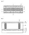
- FIG.1is a perspective view illustrating the construction of a common AC type PDP device.
- a lower plate of the PDPincludes address electrodes 2 of discharge cells, which are formed on the top surface of a lower glass substrate 1, a lower dielectric layer 3 formed on the entire address electrodes 2, barrier ribs 4, which are formed on the dielectric layer 3 and isolate the discharge cells, and phosphor layers 5 that are formed on the dielectric layer 3 and isolated by the barrier ribs 4.
- the dielectric layer 3 or the barrier ribs 4can include some reflection materials for reflecting a visible ray generated by the phosphor layers 5.
- a shield film for preventing infiltration of alkali ion contained in the glass substrate 1can be formed on the lower glass substrate 1.
- an upper plate of the plasma display panelincludes transparent electrodes 12 formed on the bottom surface of an upper glass substrate 11, bus electrodes 13 that lower resistance values of the transparent electrodes 12, a dielectric layer 14 formed on the entire top surface of the upper glass substrate 11, including the transparent electrodes 12 and the bus electrodes 13, and a protection layer 15 which is formed on the entire surface of the dielectric layer 14 and protects the dielectric layer 14 depending on plasma discharging.
- the upper plate formedthus is disposed so that the protection layer 15 faces the barrier ribs 4 and the phosphor layer 5 of the lower plate.
- electrodes composed of a pair of the transparent electrode 12 and the bus electrode 13operate as a scan electrode and a sustain electrode, and generate a discharge due to a difference in voltage provided thereto.
- the phosphor layer 5 within the discharge cellis excited by ultraviolet generated, thus generating a visible ray.
- the plasma display panelimplements the gray scale necessary for displaying an image by controlling a discharge sustaining period depending on video data, i.e., the number of a sustain discharge.
- a method of driving such a plasma display panelusually employs an ADS (Address and Display Separation) driving method in which the device is driven with it being divided into a screen non-display period and a screen display period, i.e., a discharge sustaining period.
- ADSAddress and Display Separation
- one frameis divided into the n number of bits, and each of sub-fields is divided into a reset period, an address period and a sustain period.
- the reset periodis a period where an initial condition is set so that next addressing is possible.
- wall chargesare allowed to have a constant state right before the address period in order for each cell to operate stably with uniform brightness.
- the address periodis a period where cell to be turned on and cells to be turned off are selected according to a data pulse.
- the sustain periodis a period where a discharge for cells which are turned on in the address period is maintained.
- the screenis not displayed during the reset period and the address period. In this connection, this can be called a 'non-display period'. Furthermore, the screen is displayed during the sustain period. Thus, this can be called a 'display period'.
- the period where the screen is actually displayedis a discharge sustain period, i.e., a screen display period. It will be an ideal one that during the reset and address periods where cells to be discharged are selected before the sustain period, emission due to the discharge is not generated. However, actually, since cells of the whole panel region are initialized during the reset and address periods, a weak discharge is generated. This causes the black brightness of the panel to increase. Accordingly, the contrast characteristic of an image is degraded and the clearness is thus lowered.
- the conventional plasma display panelemploys the driving method in which the device is driven with it being divided into the non-display period where cells to be discharged are initialized and selected and the display period where a discharge is sustained and the screen is thus displayed.
- the present inventionhas been made in view of the above problems, and it is an object of the present invention to provide an optical shutter for a plasma display panel in which the optical shutter, which employs a black organic solution that moves according to the electrowetting phenomenon, is formed on a display surface of the plasma display panel, wherein during the non-display period, voltages are not applied to the optical shutter so that light emitted from the panel does not transmit the optical shutter, and during the display period, voltages having a different polarity are applied to electrodes of the optical shutter so that light emitted from the panel can transmit the optical shutter, whereby a reduction in the contrast characteristic due to a weak discharge is prevented, and a driving method thereof.
- an optical shutter for a plasma display panelincluding: a first transparent substrate, which includes a first electrode pattern and a dielectric layer having a hydrophobic property surface, barrier ribs formed on the dielectric layer for separating operating regions, a black organic solution and an aqueous solution both of which fill spaces between the barrier ribs, and a second transparent substrate, which is formed on the barrier ribs and has a second electrode pattern.
- the dielectric layeris formed using polyimide or parylene and is below 10 ⁇ m in thickness, wherein fluorine based polymer of below 0.1 ⁇ m is coated on the dielectric layer so as to form the hydrophobic property surface.
- the aqueous solutionis a solution in which distilled water or electrolyte is dissolved, and if the aqueous solution in which the electrolyte is dissolved is used, the concentration of the electrolyte is below 0.3 mol/liter.
- the organic solutionis a solution in which a black non-polarity dye is dissolved using alkane of 10 to 16 in the carbon number as a solvent.
- the first electrode pattern and the second electrode patternare symmetric to each other, and if voltages are applied to the first electrode pattern and the second electrode pattern, portions in which a black organic solution is concentrated are portions in which the respective electrodes are patterned and removed.
- portions in which electrodes of the first electrode pattern and the second electrode pattern are removedare coincident with the location of the black matrix formed in an upper plate of a plasma display panel.
- the first transparent substrate the second transparent substrateare a glass composition or a film (PET, PE, etc.).
- a method of driving an optical shutter for a plasma display panelincluding the steps of: during a non-display period where cells are initialized and selected for driving the panel, allowing an organic solution to block light emitted from the panel, and during a display period where the cells selected during the non-display period are light-emitted, applying voltages having a different polarity to electrodes of the optical shutter, whereby light emitted from the panel transmits portions of the optical shutter from which the organic solution is removed.
- the voltages for driving the optical shutterare at least 80V, preferably over 100V.
- the optical shutterwhich employs the black organic solution that moves according to the electrowetting phenomenon and has the pair of the electrodes for supplying voltages, is formed on the display surface of the plasma display panel.
- voltagesare not applied to the optical shutter so that light emitted from the panel does not transmit the optical shutter.
- voltages having a different polarityare applied to the electrodes of the optical shutter so that light emitted from the panel can transmit the optical shutter. It is thus possible to completely prevent weak emission generating during the non-display period where cells are initialized and selected. Accordingly, the present invention is advantageous in that it can improve contrast and thus enhance the picture quality.
- FIG. 2is a plan view illustrating the plasma display panel to which the optical shutter according to an embodiment of the present invention is applied.
- the optical shutterincludes barrier ribs 24 for defining operating regions and physically supporting components, which are disposed between a first substrate 21 having a first electrode 22 and a dielectric layer 23 having a hydrophobic property surface, and a second substrate 28 having a second electrode 27.
- An aqueous solution 26 and an organic solution 25are injected into the regions between the barrier ribs 24.
- the optical shutteris thus completed.
- the organic solution 25, which blocks the front display surface,is a material through which light cannot transmit.
- the organic solutionhas a black non-polarity dye dissolved in by using alkane of 10 to 16 in the carbon number as a solvent. Furthermore, the remaining portions in the regions are filled with a transparent aqueous solution 26 in which distilled water or electrolyte is dissolved.
- the organic solution 25is heavier than the aqueous solution 26.
- the organic solution 25widely spreads on the dielectric layer 23 having the hydrophobic property surface, thereby blocking light from the plasma display panel.
- the barrier ribs 24can be coincident with the barrier ribs 4 (see FIG. 1) of the plasma display panel so as to separate the operating regions of the optical shutter in a cell unit.
- the first electrode 22 and the second electrode 27are patterned to form a region where the electrodes are removed.
- the organic solution 25is concentrated in the region where the electrodes are not formed.
- the organic solution 25is thus removed from the dielectric layer 23 having the hydrophobic property surface in the region where the electrodes are formed. Therefore, if voltages are applied, the optical shutter is opened, and light emitted from the plasma display panel can thus transmit the optical shutter.
- a material used for fabricating the optical shuttermust be a transparent material, except for the organic solution 25 in which the black non-polarity dye is mixed.
- the first substrate 21 and the second substrate 28can be formed using a glass material or a transparent film (i.e., PET, PE, etc.).
- the first electrode 22 and the second electrode 27can be formed using a material (i.e., ITO or ZnO) having a high transmissivity.
- the dielectric layer 23 having the hydrophobic property surfacecan be formed using polyimide or parylene, and is below 10 ⁇ m in thickness. Fluorine based polymer of 0.1 ⁇ m is coated on the dielectric layer 23 in order to form the hydrophobic property surface.
- the aqueous solution 26is formed using the aqueous solution in which distilled water or electrolyte are dissolved. If the aqueous solution in which the electrolyte is dissolved is used, the concentration of the electrolyte has to be below 0.3 mol/liter.
- FIG. 3is a plan view illustrating the pattern of the first electrode 22, which defines the region in which the organic solution 25 pushed by the electrowetting phenomenon can be concentrated.
- the electrodesare insulated since some of the electrodes are shown. It is, however, to be noted that all the electrodes are electrically connected at the boundary portions of the entire optical shutter and can be thus driven by a single electrode in a batch manner. Of course, the electrodes can be divided for individual driving. Thus, the present invention is not limited to a specific electrical circuit configuration.
- the transparent first electrode 22is patterned to form the region in which the organic solution can be concentrated when the optical shutter operates.
- a portion, which was patterned and removed,is preferably coincident with the black matrix formed in the upper plate of the plasma display panel to which the optical shutter is applied. Therefore, a light-emitting region of an existing plasma display panel can be preserved by maximum because the portion where the organic solution is concentrated by the operation of the optical shutter does not block the light-emitting region.
- the organic solution 25 and the aqueous solution 26are filled.
- the second substrate 28 having the second electrode 27 formed onis then disposed. In this state, if the pattern is viewed from line A-A', the cross section of the optical shutter shown in FIG. 2 is obtained. That is, if voltages are not applied to the electrodes, the organic solution 25 spreads on the entire regions as well as the first electrode 22 portion and the portion where the first electrode 22 is patterned, thus blocking light from transmitting the optical shutter.
- FIGS. 4 and 5are views illustrating movements of the organic solution 25 when voltages are applied to the first electrode 22 and the second electrode 27.
- FIG. 4is a cross-sectional view taken along line B-B' in FIG. 3
- FIG. 5is a cross-sectional view taken along line C-C' in FIG. 3.
- the organic solution 25is concentrated over the dielectric layer 23 at the portions where the first electrode 22 and the second electrode 27 are removed.
- FIG. 5which is a cross-sectional view vertical to a corresponding direction, it can be seen that the organic solution 25 is concentrated at the portions where the first electrode 22 and the second electrode 27 are patterned and the organic solution 25 is all pushed out from the remaining portions (portions where the electrodes are formed). Therefore, while voltages are applied, light can transmit the optical shutter.
- the region in which the electrodes are formedis coincident with the light-emitting region of the plasma display panel at which the optical shutter is located. Thus, light can be emitted without loss relatively.
- whether to display the screen of the plasma display panelcan be decided by controlling the time when the voltages are applied to the first and second electrodes of the optical shutter. If the optical shutter keeps closed by not allowing the voltages to the optical shutter during the screen non-display period where cells to be displayed are initialized and selected, a weak emitting light can be blocked. Then, during the screen display period, the optical shutter keeps opened by applying the voltages to the optical shutter. Therefore, a display image can be outputted.
- the contrast of the screencan be improved significantly and the clearness of the screen can be significantly improved accordingly.
Landscapes
- Physics & Mathematics (AREA)
- Engineering & Computer Science (AREA)
- Plasma & Fusion (AREA)
- General Physics & Mathematics (AREA)
- Optics & Photonics (AREA)
- Control Of Indicators Other Than Cathode Ray Tubes (AREA)
- Control Of Gas Discharge Display Tubes (AREA)
- Electrochromic Elements, Electrophoresis, Or Variable Reflection Or Absorption Elements (AREA)
- Devices For Indicating Variable Information By Combining Individual Elements (AREA)
- Vessels, Lead-In Wires, Accessory Apparatuses For Cathode-Ray Tubes (AREA)
- Gas-Filled Discharge Tubes (AREA)
Abstract
Description
This Nonprovisional application claims priority under 35 U.S.C. § 119(a) onPatent Application No. 10-2003-0089830 filed in Korea on December 10, 2003, theentire contents of which are hereby incorporated by reference.
The present invention relates to an optical shutter for a plasma display panel anddriving method thereof. More particularly, the present invention relates to an opticalshutter for a plasma display panel in which the optical shutter that can be selectivelydriven according to the electrowetting phenomenon is formed on a light-emitting unit ofthe plasma display panel, and the optical shutter is opened only during a display period,whereby contrast is improved, and a driving method thereof.
Recently, the size of a plasma display panel (hereinafter, referred to as 'PDP')being a large-screen digital wall mount type television has increased from 30 to 76inches. PDP manufacturers are in keen competition with one another in order to realizethe low price.
A PDP device, which has been spotlighted as a next-generation displaydevice along with a TFT LCD, organic EL, FED and the like, is a display device thatemploys a light-emitting phenomenon generating due to a difference in energywhen red (R), green (G) and blue (B) phosphors return from an excited state to aground state if the phosphors are excited with ultraviolet of 147nm generatedduring the discharge of a gas such as He+Xe or Ne+Xe within discharge cellsisolated by barrier ribs.
This PDP can have a variety of structures depending on its implementationmethod. However, most of the PDPs have a similar structure in which an electrodebus for driving each cell is disposed and a phosphor layer to be light-emitted byeach cell is coated in cell regions isolated by barrier ribs.
FIG.1 is a perspective view illustrating the construction of a common ACtype PDP device.
A lower plate of the PDP includesaddress electrodes 2 of discharge cells,which are formed on the top surface of a lower glass substrate 1, a lower dielectriclayer 3 formed on theentire address electrodes 2, barrier ribs 4, which are formedon the dielectric layer 3 and isolate the discharge cells, andphosphor layers 5 thatare formed on the dielectric layer 3 and isolated by the barrier ribs 4. The dielectriclayer 3 or the barrier ribs 4 can include some reflection materials for reflecting avisible ray generated by thephosphor layers 5. A shield film for preventinginfiltration of alkali ion contained in the glass substrate 1 can be formed on thelower glass substrate 1.
Furthermore, an upper plate of the plasma display panel includestransparentelectrodes 12 formed on the bottom surface of anupper glass substrate 11,bus electrodes 13 that lower resistance values of thetransparent electrodes 12, adielectric layer 14 formed on the entire top surface of theupper glass substrate 11,including thetransparent electrodes 12 and thebus electrodes 13, and aprotectionlayer 15 which is formed on the entire surface of thedielectric layer 14 andprotects thedielectric layer 14 depending on plasma discharging. The upper plateformed thus is disposed so that theprotection layer 15 faces the barrier ribs 4 andthephosphor layer 5 of the lower plate.
In the construction of the upper plate of the conventional plasma displaypanel, electrodes composed of a pair of thetransparent electrode 12 and thebuselectrode 13 operate as a scan electrode and a sustain electrode, and generate adischarge due to a difference in voltage provided thereto. In this time, thephosphorlayer 5 within the discharge cell is excited by ultraviolet generated, thus generatinga visible ray. In this case, the plasma display panel implements the gray scalenecessary for displaying an image by controlling a discharge sustaining perioddepending on video data, i.e., the number of a sustain discharge.
A method of driving such a plasma display panel usually employs an ADS(Address and Display Separation) driving method in which the device is driven withit being divided into a screen non-display period and a screen display period, i.e., adischarge sustaining period. In the ADS driving method, one frame is divided intothe n number of bits, and each of sub-fields is divided into a reset period, anaddress period and a sustain period.
In this time, the reset period is a period where an initial condition is set sothat next addressing is possible. In this period, wall charges are allowed to have a constant state right before the address period in order for each cell to operatestably with uniform brightness.
The address period is a period where cell to be turned on and cells to beturned off are selected according to a data pulse. The sustain period is a periodwhere a discharge for cells which are turned on in the address period is maintained.
The screen is not displayed during the reset period and the address period. Inthis connection, this can be called a 'non-display period'. Furthermore, the screen isdisplayed during the sustain period. Thus, this can be called a 'display period'.
Accordingly, the period where the screen is actually displayed is a dischargesustain period, i.e., a screen display period. It will be an ideal one that during thereset and address periods where cells to be discharged are selected before thesustain period, emission due to the discharge is not generated. However, actually,since cells of the whole panel region are initialized during the reset and addressperiods, a weak discharge is generated. This causes the black brightness of thepanel to increase. Accordingly, the contrast characteristic of an image is degradedand the clearness is thus lowered.
As stated previously, the conventional plasma display panel employs thedriving method in which the device is driven with it being divided into the non-displayperiod where cells to be discharged are initialized and selected and thedisplay period where a discharge is sustained and the screen is thus displayed. Thismakes contrast degraded because the weak discharge is generated in the non-displayperiod where the screen is not displayed actually. Accordingly, there areproblems in that the clearness decreases and the display quality is degradedaccordingly.
[Accordingly, the present invention has been made in view of the aboveproblems, and it is an object of the present invention to provide an optical shutterfor a plasma display panel in which the optical shutter, which employs a blackorganic solution that moves according to the electrowetting phenomenon, isformed on a display surface of the plasma display panel, wherein during the non-displayperiod, voltages are not applied to the optical shutter so that light emittedfrom the panel does not transmit the optical shutter, and during the display period,voltages having a different polarity are applied to electrodes of the optical shutterso that light emitted from the panel can transmit the optical shutter, whereby areduction in the contrast characteristic due to a weak discharge is prevented, and adriving method thereof.
To achieve the above object, according to the present invention, there isprovided an optical shutter for a plasma display panel, including: a first transparentsubstrate, which includes a first electrode pattern and a dielectric layer having ahydrophobic property surface, barrier ribs formed on the dielectric layer forseparating operating regions, a black organic solution and an aqueous solution bothof which fill spaces between the barrier ribs, and a second transparent substrate,which is formed on the barrier ribs and has a second electrode pattern.
In the optical shutter for the plasma display panel according to the presentinvention, the dielectric layer is formed using polyimide or parylene and is below10 µm in thickness, wherein fluorine based polymer of below 0.1 µm is coated on thedielectric layer so as to form the hydrophobic property surface.
In the optical shutter for the plasma display panel according to the presentinvention, the aqueous solution is a solution in which distilled water or electrolyte isdissolved, and if the aqueous solution in which the electrolyte is dissolved is used,the concentration of the electrolyte is below 0.3 mol/liter.
In the optical shutter for the plasma display panel according to the presentinvention, the organic solution is a solution in which a black non-polarity dye isdissolved using alkane of 10 to 16 in the carbon number as a solvent.
In the optical shutter for the plasma display panel according to the presentinvention, the first electrode pattern and the second electrode pattern aresymmetric to each other, and if voltages are applied to the first electrode patternand the second electrode pattern, portions in which a black organic solution isconcentrated are portions in which the respective electrodes are patterned andremoved.
In the optical shutter for the plasma display panel according to the presentinvention, portions in which electrodes of the first electrode pattern and the secondelectrode pattern are removed are coincident with the location of the black matrixformed in an upper plate of a plasma display panel.
In the optical shutter for the plasma display panel according to the presentinvention, the first transparent substrate the second transparent substrate are aglass composition or a film (PET, PE, etc.).
According to the present invention, there is provided a method of driving anoptical shutter for a plasma display panel, including the steps of: during a non-displayperiod where cells are initialized and selected for driving the panel, allowingan organic solution to block light emitted from the panel, and during a display period where the cells selected during the non-display period are light-emitted,applying voltages having a different polarity to electrodes of the optical shutter,whereby light emitted from the panel transmits portions of the optical shutter fromwhich the organic solution is removed.
In the method for driving the optical shutter for the plasma display panelaccording to the present invention, the voltages for driving the optical shutter areat least 80V, preferably over 100V.
As described above, the optical shutter, which employs the black organicsolution that moves according to the electrowetting phenomenon and has the pairof the electrodes for supplying voltages, is formed on the display surface of theplasma display panel. In this state, during the non-display period, voltages are notapplied to the optical shutter so that light emitted from the panel does not transmitthe optical shutter. Furthermore, during the display period, voltages having adifferent polarity are applied to the electrodes of the optical shutter so that lightemitted from the panel can transmit the optical shutter. It is thus possible tocompletely prevent weak emission generating during the non-display period wherecells are initialized and selected. Accordingly, the present invention is advantageousin that it can improve contrast and thus enhance the picture quality.
Further objects and advantages of the invention can be more fullyunderstood from the following detailed description taken in conjunction with theaccompanying drawings in which:
Preferred embodiments of the present invention will be described in a moredetailed manner with reference to the drawings.
FIG. 2 is a plan view illustrating the plasma display panel to which theoptical shutter according to an embodiment of the present invention is applied.
The construction of the optical shutter formed on anupper substrate 11 willbe described with reference to FIG. 2. The optical shutter includesbarrier ribs 24for defining operating regions and physically supporting components, which aredisposed between afirst substrate 21 having afirst electrode 22 and adielectriclayer 23 having a hydrophobic property surface, and asecond substrate 28 havingasecond electrode 27. Anaqueous solution 26 and anorganic solution 25 areinjected into the regions between thebarrier ribs 24. The optical shutter is thuscompleted. Theorganic solution 25, which blocks the front display surface, is a material through which light cannot transmit. The organic solution has a black non-polaritydye dissolved in by using alkane of 10 to 16 in the carbon number as asolvent. Furthermore, the remaining portions in the regions are filled with atransparentaqueous solution 26 in which distilled water or electrolyte is dissolved.
Theorganic solution 25 is heavier than theaqueous solution 26. Thus, in thecase where the optical shutter does not operate, theorganic solution 25 widelyspreads on thedielectric layer 23 having the hydrophobic property surface, therebyblocking light from the plasma display panel. Thebarrier ribs 24 can be coincidentwith the barrier ribs 4 (see FIG. 1) of the plasma display panel so as to separate theoperating regions of the optical shutter in a cell unit.
In the construction described above, if voltages of 80V or more (preferably,over 100V), which have a different polarity, are applied to thefirst electrode 22and thesecond electrode 27, the contact characteristic between thedielectric layer 23 having the hydrophobic property surface and theorganic solution 25 varies.Such variation in the contact characteristic between a solid having the hydrophobicproperty and a liquid, which is caused by these voltages, is called "electrowettingphenomenon". The present invention utilizes this electrowetting phenomenon.
Thefirst electrode 22 and thesecond electrode 27 are patterned to form aregion where the electrodes are removed. In this state, if voltages are applied, theorganic solution 25 is concentrated in the region where the electrodes are notformed. Theorganic solution 25 is thus removed from thedielectric layer 23 havingthe hydrophobic property surface in the region where the electrodes are formed.Therefore, if voltages are applied, the optical shutter is opened, and light emittedfrom the plasma display panel can thus transmit the optical shutter.
For such optical transmission property, a material used for fabricating theoptical shutter must be a transparent material, except for theorganic solution 25 inwhich the black non-polarity dye is mixed.
Thefirst substrate 21 and thesecond substrate 28 can be formed using aglass material or a transparent film (i.e., PET, PE, etc.). Thefirst electrode 22 andthesecond electrode 27 can be formed using a material (i.e., ITO or ZnO) having ahigh transmissivity.
Thedielectric layer 23 having the hydrophobic property surface can beformed using polyimide or parylene, and is below 10 µm in thickness. Fluorine basedpolymer of 0.1 µm is coated on thedielectric layer 23 in order to form thehydrophobic property surface.
As described above, theaqueous solution 26 is formed using the aqueoussolution in which distilled water or electrolyte are dissolved. If the aqueous solutionin which the electrolyte is dissolved is used, the concentration of the electrolytehas to be below 0.3 mol/liter.
FIG. 3 is a plan view illustrating the pattern of thefirst electrode 22, whichdefines the region in which theorganic solution 25 pushed by the electrowettingphenomenon can be concentrated. In FIG. 3, it looks like that the electrodes areinsulated since some of the electrodes are shown. It is, however, to be noted thatall the electrodes are electrically connected at the boundary portions of the entireoptical shutter and can be thus driven by a single electrode in a batch manner. Ofcourse, the electrodes can be divided for individual driving. Thus, the presentinvention is not limited to a specific electrical circuit configuration.
As shown in FIG. 3, the transparentfirst electrode 22 is patterned to formthe region in which the organic solution can be concentrated when the opticalshutter operates. A portion, which was patterned and removed, is preferablycoincident with the black matrix formed in the upper plate of the plasma displaypanel to which the optical shutter is applied. Therefore, a light-emitting region of anexisting plasma display panel can be preserved by maximum because the portionwhere the organic solution is concentrated by the operation of the optical shutterdoes not block the light-emitting region.
After thedielectric layer 23 is formed in thefirst electrode 22, theorganicsolution 25 and theaqueous solution 26 are filled. Thesecond substrate 28 havingthesecond electrode 27 formed on is then disposed. In this state, if the pattern isviewed from line A-A', the cross section of the optical shutter shown in FIG. 2 isobtained. That is, if voltages are not applied to the electrodes, theorganic solution 25 spreads on the entire regions as well as thefirst electrode 22 portion and theportion where thefirst electrode 22 is patterned, thus blocking light fromtransmitting the optical shutter.
FIGS. 4 and 5 are views illustrating movements of theorganic solution 25when voltages are applied to thefirst electrode 22 and thesecond electrode 27.FIG. 4 is a cross-sectional view taken along line B-B' in FIG. 3, and FIG. 5 is across-sectional view taken along line C-C' in FIG. 3.
From FIG. 4, it can be seen that theorganic solution 25 is concentrated overthedielectric layer 23 at the portions where thefirst electrode 22 and thesecondelectrode 27 are removed. From FIG. 5 which is a cross-sectional view vertical to acorresponding direction, it can be seen that theorganic solution 25 is concentrated at the portions where thefirst electrode 22 and thesecond electrode 27 arepatterned and theorganic solution 25 is all pushed out from the remaining portions(portions where the electrodes are formed). Therefore, while voltages are applied,light can transmit the optical shutter.
The region in which the electrodes are formed is coincident with the light-emittingregion of the plasma display panel at which the optical shutter is located.Thus, light can be emitted without loss relatively.
Therefore, whether to display the screen of the plasma display panel can bedecided by controlling the time when the voltages are applied to the first andsecond electrodes of the optical shutter. If the optical shutter keeps closed by notallowing the voltages to the optical shutter during the screen non-display periodwhere cells to be displayed are initialized and selected, a weak emitting light can beblocked. Then, during the screen display period, the optical shutter keeps openedby applying the voltages to the optical shutter. Therefore, a display image can beoutputted.
According to the driving method described above, the contrast of the screencan be improved significantly and the clearness of the screen can be significantlyimproved accordingly.
While the present invention has been described with reference to theparticular illustrative embodiments, it is not to be restricted by the embodimentsbut only by the appended claims. It is to be appreciated that those skilled in the artcan change or modify the embodiments without departing from the scope and spiritof the present invention.
The claims refer to examples of preferred embodiments of the invention.However, the invention also refers to the use of any single feature and subcombinationof features which are disclosed in the claims, the description and/or the drawings.
Claims (12)
- An optical shutter, comprising:a first transparent substrate having a first electrode pattern and a dielectriclayer;barrier ribs formed on the dielectric layer for separating operating regions;solutions that fill spaces between the barrier ribs; anda second transparent substrate, which is formed on the barrier ribs and has asecond electrode pattern.
- The optical shutter according to claim 1, wherein the dielectric layer has ahydrophobic property surface.
- The optical shutter according to claim 1, wherein the solutions include ablack organic solution and an aqueous solution.
- An optical shutter, comprising:a first transparent substrate, which includes a first electrode pattern and adielectric layer having a hydrophobic property surface;barrier ribs, which are formed on the dielectric layer and separate operatingregionsa black organic solution and an aqueous solution both of which fill spacesbetween the barrier ribs; anda second transparent substrate, which is formed on the barrier ribs and has asecond electrode pattern.
- The optical shutter according to claim 4, wherein the dielectric layer isformed using polyimide or parylene and is below 10 µm in thickness, whereinfluorine based polymer of below 0.1 µm is coated on the dielectric layer so as toform the hydrophobic property surface.
- The optical shutter according to claim 4, wherein the aqueous solution isa solution in which distilled water or electrolyte is dissolved, and if the aqueoussolution in which the electrolyte is dissolved is used, the concentration of theelectrolyte is below 0.3 mol/liter.
- The optical shutter according to claim 4, wherein the organic solution is asolution in which a black non-polarity dye is dissolved using alkane of 10 to 16 inthe carbon number as a solvent.
- The optical shutter according to claim 4, wherein the first electrodepattern and the second electrode pattern are symmetric to each other, and ifvoltages are applied to the first electrode pattern and the second electrode pattern,portions in which a black organic solution is concentrated are portions in which therespective electrodes are patterned and removed.
- The optical shutter according to claim 4, wherein portions in whichelectrodes of the first electrode pattern and the second electrode pattern are removed are coincident with the location of the black matrix formed in an upperplate of a plasma display panel.
- The optical shutter according to claim 4, wherein the first transparentsubstrate the second transparent substrate are a glass composition or a film (PET,PE, etc.).
- A method of driving an organic solution optical shutter disposed on adisplay surface of a plasma display panel, comprising the steps of:(a) during a non-display period where cells are initialized and selected fordriving the panel, allowing an organic solution to block light emitted from the panel;and(b) during a display period where the cells selected during the non-displayperiod are light-emitted, applying voltages having a different polarity to electrodesof the optical shutter, whereby light emitted from the panel transmits portions ofthe optical shutter from which the organic solution is removed.
- The method according to claim 11, wherein the voltages for driving theoptical shutter are at least 80V, preferably over 100V.
Applications Claiming Priority (2)
| Application Number | Priority Date | Filing Date | Title |
|---|---|---|---|
| KR2003089830 | 2003-12-10 | ||
| KR10-2003-0089830AKR100531796B1 (en) | 2003-12-10 | 2003-12-10 | Optical shutter for plasma display panel and driving method therof |
Publications (2)
| Publication Number | Publication Date |
|---|---|
| EP1542056A2true EP1542056A2 (en) | 2005-06-15 |
| EP1542056A3 EP1542056A3 (en) | 2005-10-26 |
Family
ID=34511210
Family Applications (1)
| Application Number | Title | Priority Date | Filing Date |
|---|---|---|---|
| EP04028863AWithdrawnEP1542056A3 (en) | 2003-12-10 | 2004-12-06 | Optical shutter for plasma display panel and driving method thereof |
Country Status (5)
| Country | Link |
|---|---|
| US (1) | US7315411B2 (en) |
| EP (1) | EP1542056A3 (en) |
| JP (1) | JP2005173605A (en) |
| KR (1) | KR100531796B1 (en) |
| CN (1) | CN1627467A (en) |
Cited By (5)
| Publication number | Priority date | Publication date | Assignee | Title |
|---|---|---|---|---|
| WO2005122876A1 (en)* | 2004-06-16 | 2005-12-29 | Carl Zeiss Surgical Gmbh | Variable diaphragm, illumination device, optical observation device and optical observation appliance |
| WO2007071904A1 (en)* | 2005-12-22 | 2007-06-28 | Eastman Kodak Company | Display devices |
| EP2034351A1 (en) | 2007-09-05 | 2009-03-11 | Sony Corporation | Lighting system |
| WO2009072871A1 (en)* | 2007-12-06 | 2009-06-11 | Miortech Holding B.V. | Electrowetting element |
| EP2637057A1 (en)* | 2012-03-05 | 2013-09-11 | Sick Ag | Light source for a sensor and distance measuring optoelectronic sensor |
Families Citing this family (49)
| Publication number | Priority date | Publication date | Assignee | Title |
|---|---|---|---|---|
| US7417782B2 (en) | 2005-02-23 | 2008-08-26 | Pixtronix, Incorporated | Methods and apparatus for spatial light modulation |
| US7746529B2 (en) | 2005-02-23 | 2010-06-29 | Pixtronix, Inc. | MEMS display apparatus |
| US8482496B2 (en) | 2006-01-06 | 2013-07-09 | Pixtronix, Inc. | Circuits for controlling MEMS display apparatus on a transparent substrate |
| US20070205969A1 (en) | 2005-02-23 | 2007-09-06 | Pixtronix, Incorporated | Direct-view MEMS display devices and methods for generating images thereon |
| US9261694B2 (en) | 2005-02-23 | 2016-02-16 | Pixtronix, Inc. | Display apparatus and methods for manufacture thereof |
| US7999994B2 (en) | 2005-02-23 | 2011-08-16 | Pixtronix, Inc. | Display apparatus and methods for manufacture thereof |
| US8159428B2 (en) | 2005-02-23 | 2012-04-17 | Pixtronix, Inc. | Display methods and apparatus |
| US8519945B2 (en) | 2006-01-06 | 2013-08-27 | Pixtronix, Inc. | Circuits for controlling display apparatus |
| US7405852B2 (en) | 2005-02-23 | 2008-07-29 | Pixtronix, Inc. | Display apparatus and methods for manufacture thereof |
| US7304786B2 (en) | 2005-02-23 | 2007-12-04 | Pixtronix, Inc. | Methods and apparatus for bi-stable actuation of displays |
| US9158106B2 (en) | 2005-02-23 | 2015-10-13 | Pixtronix, Inc. | Display methods and apparatus |
| US8310442B2 (en) | 2005-02-23 | 2012-11-13 | Pixtronix, Inc. | Circuits for controlling display apparatus |
| US9087486B2 (en) | 2005-02-23 | 2015-07-21 | Pixtronix, Inc. | Circuits for controlling display apparatus |
| US7304785B2 (en) | 2005-02-23 | 2007-12-04 | Pixtronix, Inc. | Display methods and apparatus |
| US9229222B2 (en) | 2005-02-23 | 2016-01-05 | Pixtronix, Inc. | Alignment methods in fluid-filled MEMS displays |
| US9082353B2 (en) | 2010-01-05 | 2015-07-14 | Pixtronix, Inc. | Circuits for controlling display apparatus |
| KR100646815B1 (en)* | 2005-11-30 | 2006-11-23 | 이미지랩(주) | Electrowetting display device |
| KR100646810B1 (en)* | 2005-11-30 | 2006-11-23 | 이미지랩(주) | Emissive electrowetting display device |
| US8526096B2 (en) | 2006-02-23 | 2013-09-03 | Pixtronix, Inc. | Mechanical light modulators with stressed beams |
| KR101252845B1 (en)* | 2006-03-29 | 2013-04-09 | 엘지디스플레이 주식회사 | Image Display Device and Driving Method Thereof |
| US7876489B2 (en) | 2006-06-05 | 2011-01-25 | Pixtronix, Inc. | Display apparatus with optical cavities |
| EP2080045A1 (en) | 2006-10-20 | 2009-07-22 | Pixtronix Inc. | Light guides and backlight systems incorporating light redirectors at varying densities |
| JP2008170962A (en)* | 2006-12-14 | 2008-07-24 | Sony Corp | Optical shutter for display, image display device, and equipment and method of manufacturing optical shutter for display |
| US7636187B2 (en) | 2006-12-14 | 2009-12-22 | Sony Corporation | Optical shutter for display device, image display apparatus, and apparatus and method for manufacturing the optical shutter |
| CN101206377B (en)* | 2006-12-20 | 2010-05-26 | 鸿富锦精密工业(深圳)有限公司 | Aperture |
| US7852546B2 (en) | 2007-10-19 | 2010-12-14 | Pixtronix, Inc. | Spacers for maintaining display apparatus alignment |
| US9176318B2 (en) | 2007-05-18 | 2015-11-03 | Pixtronix, Inc. | Methods for manufacturing fluid-filled MEMS displays |
| KR100873283B1 (en) | 2007-01-30 | 2008-12-11 | 전북대학교산학협력단 | Total color electro wetting display |
| CN101355838B (en)* | 2007-07-25 | 2010-12-29 | 群康科技(深圳)有限公司 | Electric moistening display |
| CN101359091B (en)* | 2007-08-03 | 2010-09-29 | 群康科技(深圳)有限公司 | Electrowetting display and manufacturing method thereof |
| CN101493576B (en)* | 2008-01-23 | 2010-12-15 | 财团法人工业技术研究院 | Electrowetting display device and method of manufacturing the same |
| KR100941844B1 (en)* | 2008-01-29 | 2010-02-11 | 삼성에스디아이 주식회사 | Film filter and flat panel display device having the same |
| JP2009211047A (en)* | 2008-02-05 | 2009-09-17 | Sony Corp | Liquid optical element |
| US8248560B2 (en) | 2008-04-18 | 2012-08-21 | Pixtronix, Inc. | Light guides and backlight systems incorporating prismatic structures and light redirectors |
| TWI418848B (en)* | 2008-08-29 | 2013-12-11 | Prime View Int Co Ltd | Pixel structure for use in a display and display using the same |
| US8169679B2 (en) | 2008-10-27 | 2012-05-01 | Pixtronix, Inc. | MEMS anchors |
| TW201033640A (en)* | 2009-03-03 | 2010-09-16 | Ind Tech Res Inst | Electrowetting display devices |
| TWI407146B (en)* | 2009-06-10 | 2013-09-01 | Ind Tech Res Inst | Electrowetting display and method for fabricating the same |
| JP5568902B2 (en)* | 2009-06-24 | 2014-08-13 | 株式会社リコー | Display element |
| KR20120132680A (en) | 2010-02-02 | 2012-12-07 | 픽스트로닉스 인코포레이티드 | Methods for manufacturing cold seal fluid-filled display apparatus |
| US8723759B2 (en) | 2010-06-23 | 2014-05-13 | Sharp Kabushiki Kaisha | Display with light concentrating substrate |
| JP6140397B2 (en)* | 2011-06-10 | 2017-05-31 | 三星電子株式会社Samsung Electronics Co.,Ltd. | Electromagnetic wave generator and electromagnetic wave generator array |
| JP2013003480A (en)* | 2011-06-21 | 2013-01-07 | Sony Corp | Display and electronic apparatus |
| US9134552B2 (en) | 2013-03-13 | 2015-09-15 | Pixtronix, Inc. | Display apparatus with narrow gap electrostatic actuators |
| TWI485430B (en)* | 2013-10-29 | 2015-05-21 | Au Optronics Corp | Electrowetting display device |
| US9696482B2 (en) | 2013-12-30 | 2017-07-04 | Google Technology Holdings LLC | Backlight dimming film |
| JP6659447B2 (en) | 2016-05-02 | 2020-03-04 | 浜松ホトニクス株式会社 | Distance sensor |
| CN111258054A (en)* | 2020-03-30 | 2020-06-09 | 深圳市华星光电半导体显示技术有限公司 | Quantum dot display device and manufacturing method thereof |
| US11210972B1 (en)* | 2020-12-23 | 2021-12-28 | New Visual Media Group, L.L.C. | Optical shutter and display panel |
Family Cites Families (8)
| Publication number | Priority date | Publication date | Assignee | Title |
|---|---|---|---|---|
| US5851732A (en)* | 1997-03-06 | 1998-12-22 | E. I. Du Pont De Nemours And Company | Plasma display panel device fabrication utilizing black electrode between substrate and conductor electrode |
| KR100536868B1 (en)* | 1997-10-03 | 2006-02-28 | 다이니폰 인사츠 가부시키가이샤 | Transfer sheet |
| JP2000356750A (en)* | 1999-06-16 | 2000-12-26 | Canon Inc | Display element and display device |
| US6449081B1 (en)* | 1999-06-16 | 2002-09-10 | Canon Kabushiki Kaisha | Optical element and optical device having it |
| KR101166245B1 (en)* | 2001-10-11 | 2012-07-18 | 코닌클리케 필립스 일렉트로닉스 엔.브이. | 2d/3d display apparatus |
| US7359108B2 (en)* | 2003-01-27 | 2008-04-15 | Liquavista B.V. | Display device |
| EP1599752A1 (en)* | 2003-02-26 | 2005-11-30 | Koninklijke Philips Electronics N.V. | A passive matrix display with bistable electro-wetting cells |
| KR101100980B1 (en)* | 2003-05-22 | 2011-12-29 | 삼성 엘씨디 네덜란드 알앤디 센터 비.브이. | Display devices |
- 2003
- 2003-12-10KRKR10-2003-0089830Apatent/KR100531796B1/ennot_activeExpired - Fee Related
- 2004
- 2004-12-06EPEP04028863Apatent/EP1542056A3/ennot_activeWithdrawn
- 2004-12-08JPJP2004354844Apatent/JP2005173605A/ennot_activeWithdrawn
- 2004-12-09USUS11/007,176patent/US7315411B2/ennot_activeExpired - Fee Related
- 2004-12-10CNCNA2004100986553Apatent/CN1627467A/enactivePending
Cited By (8)
| Publication number | Priority date | Publication date | Assignee | Title |
|---|---|---|---|---|
| WO2005122876A1 (en)* | 2004-06-16 | 2005-12-29 | Carl Zeiss Surgical Gmbh | Variable diaphragm, illumination device, optical observation device and optical observation appliance |
| WO2007071904A1 (en)* | 2005-12-22 | 2007-06-28 | Eastman Kodak Company | Display devices |
| EP2034351A1 (en) | 2007-09-05 | 2009-03-11 | Sony Corporation | Lighting system |
| US8231249B2 (en) | 2007-09-05 | 2012-07-31 | Sony Corporation | Lighting system |
| WO2009072871A1 (en)* | 2007-12-06 | 2009-06-11 | Miortech Holding B.V. | Electrowetting element |
| WO2009072866A1 (en)* | 2007-12-06 | 2009-06-11 | Miortech Holding B.V. | Electrowetting element |
| EP2637057A1 (en)* | 2012-03-05 | 2013-09-11 | Sick Ag | Light source for a sensor and distance measuring optoelectronic sensor |
| US8810805B2 (en) | 2012-03-05 | 2014-08-19 | Sick Ag | Light source for a sensor and a distance-measuring optoelectronic sensor |
Also Published As
| Publication number | Publication date |
|---|---|
| KR20050056774A (en) | 2005-06-16 |
| CN1627467A (en) | 2005-06-15 |
| US20050128370A1 (en) | 2005-06-16 |
| KR100531796B1 (en) | 2005-12-02 |
| US7315411B2 (en) | 2008-01-01 |
| JP2005173605A (en) | 2005-06-30 |
| EP1542056A3 (en) | 2005-10-26 |
Similar Documents
| Publication | Publication Date | Title |
|---|---|---|
| US7315411B2 (en) | Optical shutter for plasma display panel and driving method thereof | |
| US7663316B2 (en) | Plasma display panel having barrier ribs with black matrix | |
| US20050093776A1 (en) | Plasma display device and method for driving same | |
| US7777694B2 (en) | Plasma display apparatus and method for driving the same | |
| CN100557672C (en) | Plasma display panel and driving method thereof | |
| US20070171151A1 (en) | Plasma display apparatus and driving method thereof | |
| KR100811472B1 (en) | Plasma display device | |
| EP1752952A1 (en) | Plasma display apparatus and method of driving the same | |
| KR100862568B1 (en) | Plasma display panel | |
| US7847758B2 (en) | Plasma display panel driving method | |
| KR100820640B1 (en) | Plasma display device | |
| US8098216B2 (en) | Plasma display apparatus and driving method thereof | |
| KR100493436B1 (en) | Driving Method of Plasma Display Panel | |
| US20060066516A1 (en) | Driving method of plasma display panel | |
| US20070046572A1 (en) | Plasma display panel (PDP) | |
| US20080012796A1 (en) | Plasma display apparatus and driving method thereof | |
| US20070035476A1 (en) | Method of driving plasma display panel and plasma display device driven using the method | |
| KR100800465B1 (en) | Plasma display device | |
| KR20060116323A (en) | Plasma display panel and driving method for driving same | |
| US7999761B2 (en) | Plasma display apparatus and method of driving the same | |
| KR100741123B1 (en) | Plasma display panel | |
| KR100692042B1 (en) | Plasma display panel | |
| US20050259045A1 (en) | Plasma display panel (PDP) | |
| KR20070121290A (en) | Plasma display device | |
| US20070222713A1 (en) | Method of driving plasma display panel |
Legal Events
| Date | Code | Title | Description |
|---|---|---|---|
| PUAI | Public reference made under article 153(3) epc to a published international application that has entered the european phase | Free format text:ORIGINAL CODE: 0009012 | |
| 17P | Request for examination filed | Effective date:20041206 | |
| AK | Designated contracting states | Kind code of ref document:A2 Designated state(s):AT BE BG CH CY CZ DE DK EE ES FI FR GB GR HU IE IS IT LI LT LU MC NL PL PT RO SE SI SK TR | |
| AX | Request for extension of the european patent | Extension state:AL BA HR LV MK YU | |
| PUAL | Search report despatched | Free format text:ORIGINAL CODE: 0009013 | |
| AK | Designated contracting states | Kind code of ref document:A3 Designated state(s):AT BE BG CH CY CZ DE DK EE ES FI FR GB GR HU IE IS IT LI LT LU MC NL PL PT RO SE SI SK TR | |
| AX | Request for extension of the european patent | Extension state:AL BA HR LV MK YU | |
| RIC1 | Information provided on ipc code assigned before grant | Ipc:7G 02F 1/17 B Ipc:7G 09G 3/22 B Ipc:7G 09F 9/37 B Ipc:7G 02B 26/02 A | |
| AKX | Designation fees paid | ||
| STAA | Information on the status of an ep patent application or granted ep patent | Free format text:STATUS: THE APPLICATION IS DEEMED TO BE WITHDRAWN | |
| 18D | Application deemed to be withdrawn | Effective date:20060427 | |
| REG | Reference to a national code | Ref country code:DE Ref legal event code:8566 |