EP1540863B1 - Staged locking of phase locked loops - Google Patents
Staged locking of phase locked loopsDownload PDFInfo
- Publication number
- EP1540863B1 EP1540863B1EP03765652AEP03765652AEP1540863B1EP 1540863 B1EP1540863 B1EP 1540863B1EP 03765652 AEP03765652 AEP 03765652AEP 03765652 AEP03765652 AEP 03765652AEP 1540863 B1EP1540863 B1EP 1540863B1
- Authority
- EP
- European Patent Office
- Prior art keywords
- clock signal
- wclk
- data
- serial data
- encoding
- Prior art date
- Legal status (The legal status is an assumption and is not a legal conclusion. Google has not performed a legal analysis and makes no representation as to the accuracy of the status listed.)
- Expired - Lifetime
Links
- 238000000034methodMethods0.000claimsdescription18
- 230000005540biological transmissionEffects0.000claimsdescription13
- 230000001360synchronised effectEffects0.000claimsdescription8
- 238000010586diagramMethods0.000description6
- 230000005236sound signalEffects0.000description5
- 230000002411adverseEffects0.000description3
- 230000006978adaptationEffects0.000description1
Images


Classifications
- H—ELECTRICITY
- H03—ELECTRONIC CIRCUITRY
- H03L—AUTOMATIC CONTROL, STARTING, SYNCHRONISATION OR STABILISATION OF GENERATORS OF ELECTRONIC OSCILLATIONS OR PULSES
- H03L7/00—Automatic control of frequency or phase; Synchronisation
- H03L7/06—Automatic control of frequency or phase; Synchronisation using a reference signal applied to a frequency- or phase-locked loop
- H03L7/16—Indirect frequency synthesis, i.e. generating a desired one of a number of predetermined frequencies using a frequency- or phase-locked loop
- H03L7/22—Indirect frequency synthesis, i.e. generating a desired one of a number of predetermined frequencies using a frequency- or phase-locked loop using more than one loop
- H03L7/23—Indirect frequency synthesis, i.e. generating a desired one of a number of predetermined frequencies using a frequency- or phase-locked loop using more than one loop with pulse counters or frequency dividers
- H—ELECTRICITY
- H03—ELECTRONIC CIRCUITRY
- H03L—AUTOMATIC CONTROL, STARTING, SYNCHRONISATION OR STABILISATION OF GENERATORS OF ELECTRONIC OSCILLATIONS OR PULSES
- H03L7/00—Automatic control of frequency or phase; Synchronisation
- H03L7/06—Automatic control of frequency or phase; Synchronisation using a reference signal applied to a frequency- or phase-locked loop
- H—ELECTRICITY
- H04—ELECTRIC COMMUNICATION TECHNIQUE
- H04J—MULTIPLEX COMMUNICATION
- H04J3/00—Time-division multiplex systems
- H—ELECTRICITY
- H04—ELECTRIC COMMUNICATION TECHNIQUE
- H04L—TRANSMISSION OF DIGITAL INFORMATION, e.g. TELEGRAPHIC COMMUNICATION
- H04L7/00—Arrangements for synchronising receiver with transmitter
- H04L7/0016—Arrangements for synchronising receiver with transmitter correction of synchronization errors
- H04L7/005—Correction by an elastic buffer
- H—ELECTRICITY
- H04—ELECTRIC COMMUNICATION TECHNIQUE
- H04L—TRANSMISSION OF DIGITAL INFORMATION, e.g. TELEGRAPHIC COMMUNICATION
- H04L7/00—Arrangements for synchronising receiver with transmitter
- H04L7/02—Speed or phase control by the received code signals, the signals containing no special synchronisation information
- H—ELECTRICITY
- H04—ELECTRIC COMMUNICATION TECHNIQUE
- H04L—TRANSMISSION OF DIGITAL INFORMATION, e.g. TELEGRAPHIC COMMUNICATION
- H04L7/00—Arrangements for synchronising receiver with transmitter
- H04L7/04—Speed or phase control by synchronisation signals
- H04L7/08—Speed or phase control by synchronisation signals the synchronisation signals recurring cyclically
Definitions
- the present inventiongenerally relates to data synchronization, and more particularly, to a technique for achieving data synchronization in devices such as a wireless audio transmitter through the staged locking of phase locked loops (PLLs).
- PLLsphase locked loops
- US2002/0030518 A1discloses a device and method for converting a first clock signal into a second clock signal having the features of claims 1 and 6, respectively.
- US 5,406,590discloses a device and method in which a phase locked loop is adapted to lock to a master clock signal, and a control means is adapted to determine whether said first phased locked loop is locked based on a comparison of phases of the master clock and an output signal of said phase locked loop.
- Data synchronizationis essential to the proper operation of certain electronic devices, such as devices which transmit and/or receive audio and/or video signals.
- devices which transmit audio signalsfor example, a lack of data synchronization may cause audio discontinuities during reproduction which adversely affects a user's listening experience.
- devices which transmit video signalsa lack of data synchronization may cause video discontinuities during reproduction which adversely affects a user's viewing experience .
- Data synchronization problems in such devicesmay be attributable to various factors. For example, with certain devices a data rate mismatch between the rate at which a device receives data and the rate at which the device transmits data may create data synchronization problems. Such data rate mismatches may for example be evident when certain data registers of the device fall to stably maintain a prescribed data fill state. When such data rate mismatches occur, the aforementioned data discontinuities may also intermittently occur and thereby adversely affect a user's listening and/or viewing experience.
- environment 100comprises computing means such as personal computer (PC) 10 and transmission means such as wireless transmitter 15.
- Wireless transmitter 15comprises control means such as streaming controller 20, encoding means such as encoder 30, radio frequency (RF) transmission means such as RF transmission circuitry 40, and signal output means such as antenna 50.
- environment 100includes elements which enable wireless transmission of audio signals.
- RFradio frequency
- environment 100includes elements which enable wireless transmission of audio signals.
- the principles of the present inventionmay also be applied to other devices, such as, but not limited to, devices which transmit video signals and devices which receive audio and/or video signals.
- PC 10is operative to perform various computing operations, and may for example be embodied as a commercially available desktop, laptop or other type of computer.
- PC 10serially outputs digital audio signals to wireless transmitter 15 via a bus such as a universal serial bus (USB).
- Wireless transmitter 15is operative to encode the digital audio signals provided from PC 10, and wirelessly transmit encoded audio signals to a receiving device (not shown), such as a Lyra audio player manufactured by Thomson.
- a receiving devicenot shown
- wireless transmitter 15performs a data synchronization process through the staged locking of PLLs, and thereby avoids audio discontinuities that negatively impact a user's listening experience.
- FIG. 2a block diagram illustrating further details of streaming controller 20 of FIG. 1 according to an exemplary embodiment of the present invention is shown.
- FIG. 2shows elements of streaming controller 20 which provide its clock management function.
- streaming controller 20comprises a serial interface engine 21, a codec port 22, a start of frame (SOF) capture counter 23, a controller 24, a PLL and clock generation circuitry 25, a frequency synthesizer 26, and clock divider circuitry 27.
- Streaming controller 20may for example be embodied as an integrated circuit (IC) such as a Texas Instruments TAS 1020.
- ICintegrated circuit
- serial interface engine 21is operative to receive data such as audio data from PC 10 and serially stream the received audio data to codec port 22. ln this process, the incoming data rate to serial interface engine 21 and the outgoing data rate from codec port 22 must be synchronized in order to avoid audio discontinuities which negatively affect a user's listening experience.
- serial interface engine 21receives a SOF signal from PC 10 every 1 millisecond indicating the start of a USB frame. These received USB frames contain audio data that conform to the compact-disk (CD) audio standard having a 44.1 kHz sample rate, a 16-bit sample size, and 2 samples per audio data frame.
- CDcompact-disk
- data synchronizationis achieved by providing codec port 22 with a 1.4112 (i.e., 44.1k * 16 * 2) MHz clock signal.
- PLL and clock generation circuitry 25provide a 48 MHz reference frequency which enables frequency synthesizer 26 to generate a clock signal which is nominally 22.5792 MHz.
- Clock divider circuitry 27receives the 22.5792 MHz clock signal from frequency synthesizer 26 and is operative to divide the 22.5792 MHz clock signal by 16 to thereby generate the 1.4112 MHz clock signal which is provided to codec port 22.
- Codec port 22uses the 1.4112 MHz clock signal to generate a 44.1 kHz word clock (WCLK) signal, and a 1.4112 MHz bit clock (BCLK) signal.
- Frequency synthesizer 26also provides the aforementioned 22.5792 MHz clock signal to SOF capture counter 23 which counts the number of 22.5792 MHz clock events per USB frame and interrupts controller 24 with a corresponding count value every 1 millisecond based on the aforementioned SOF signal provided from PC 10 via serial interface engine 21. Controller 24 is operative to create a software-based PLL that uses the count values from SOF capture counter 23 to generate a control signal which controls frequency synthesizer 26 in order to arrive at an average number of 22.5792 MHz clock events per USB frame.
- FIG. 3a block diagram illustrating further details of encoder 30 of FIG. 1 according to an exemplary embodiment of the present invention is shown.
- encoder 30comprises a serial input 31, an eight-to-fourteen bit modulation (EFM) clock generator 32, and EFM modulation circuitry 33.
- EFM clock generator 32comprises a digital/analog PLL 34, and clock divider circuitry 35.
- Encoder 30may for example be embodied as an IC such as a Philips SAA7392.
- serial input 31is operative to receive the aforementioned WCLK signal, BCLK signal, and audio data from codec port 22 of streaming controller 20 of FIG. 2 .
- the WCLK signal, BCLK signal, and audio dataare provided from codec port 22 to serial input 31 via a bus such as an inter-IC sound (I2S) bus which connects streaming controller 20 and encoder 30.
- Serial input 31streams the WCLK signal, BCLK signal, and audio data to EFM modulation circuitry 33 which includes a first-in, first-out (FIFO) register operating at 4.3218 MHz.
- FIFOfirst-in, first-out
- Serial input 31also provides the WCLK signal to EFM clock generation circuitry 32 which synchronizes to the incoming data rate by using the 44.1 kHz WCLK signal as the reference frequency for digital/analog PLL 34 and a FIFO fill state signal from EFM modulation circuitry 33 as an error signal for digital/analog PLL 34.
- digital/analog PLL 34provides a 69.1488 MHz clock signal to clock divider circuitry 35 which is operative to divide the 69.1488 MHz clock signal by 16 to thereby generate the 4.3218 MHz clock signal which is provided to the FIFO register of EFM modulation circuitry 33.
- digital/analog PLL 34is locked to the 44.1 kHz reference frequency of the WCLK signal when its analog PLL input frequency is between 100 and 140 MHz.
- the FIFO fill state signal from EFM modulation circuitry 33should stably indicate a fill state between 5856 and 6120 bytes.
- controller 24 of streaming controller 20detects when the analog PLL input frequency of digital/analog PLL 34 and the FIFO fill state of EFM modulation circuitry 33 are within the prescribed ranges indicated above by reading these frequency and fill state values via a bi-directional bus such as an inter-IC (I2C) bus which connects streaming controller 20 and encoder 30.
- I2Cinter-IC
- controller 24 of streaming controller 20enables audio data to be streamed from PC 10 to encoder 30 for EFM encoding.
- EFM modulation circuitry 33 of encoder 30then provides EFM encoded data to RF transmission circuitry 40 for.wireless transmission via antenna 50 to a receiving device (not shown), such as a Lyra audio player manufactured by Thomson Inc.
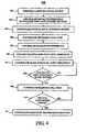
- FIG. 4a flowchart 400 illustrating steps according to an exemplary embodiment of the present invention is shown.
- the steps of FIG. 4will be described with reference to PC 10, streaming controller 20, and encoder 30 of FIGS. 1 to 3 .
- the steps of FIG. 4are merely exemplary, and are not intended to limit the present invention in any manner.
- PC 10initializes the bus connecting it to wireless transmitter 15. As previously indicated herein, this bus may for example represent a USB which is generally known in the art.
- controller 24 of streaming controller 20initializes frequency synthesizer 26 and clock divider circuitry 27 by providing initialization signals thereto.
- controller 24enables serial interface engine 21 by providing an enabling signal thereto.
- controller 24initializes codec port 22 by providing an initialization signal thereto.
- controller 24enables SOF interrupts by configuring itself to be interrupted by SOF capture counter 23.
- SOF capture counter 23counts the number of 22.5792 MHz clock events per USB frame and interrupts controller 24 with a corresponding count value every 1 millisecond based on the aforementioned SOF signal provided from PC 10 via serial interface engine 21.
- controller 24initializes EFM clock generator 32 of encoder 30 by providing an initialization signal to digital/analog PLL 34 via the I2C bus which connects streaming controller 20 and encoder 30.
- controller 24reads the analog PLL input frequency from digital/analog PLL 34 via the I2C bus.
- controller 24determines whether the analog PLL input frequency read at step 407 is within its prescribed range.
- the analog PLL input frequency of digital/analog PLL 34is within its prescribed range according to an exemplary embodiment of the present invention when it is between 100 and 140 MHz.
- process flowloops back to step 407 where controller 24 again reads the analog PLL input frequency from digital/analog PLL 34 via the I2C bus. In this manner, steps 407 and 408 are repeated until controller 24 determines that the analog PLL input frequency of digital/analog PLL 34 is within its prescribed range. Once the analog PLL input frequency is within its prescribed range, process flow advances to step 409.
- controller 24reads the FIFO fill state from EFM modulation circuitry 33 via the I2C bus.
- controller 24determines whether the FIFO fill state read at step 409 is within its prescribed range. As previously indicated herein, the FIFO fill state of EFM modulation circuitry 33 is within its prescribed range according to an exemplary embodiment of the present invention when it is between 5856 and 6120 bytes. When the determination at step 410 is negative, process flow loops back to step 409 where controller 24 again reads the FIFO fill state from EFM modulation circuitry 33 via the I2C bus. In this manner, steps 409 and 410 are repeated until controller 24 determines that the FIFO fill state of EFM modulation circuitry 33 is within its prescribed range. Once the FIFO fill state is within its prescribed range, process flow advances to step 411 where controller 24 enables RF transmission circuitry 40 by providing an enabling signal thereto.
- data such as audio datamay be synchronously streamed without discontinuities from PC 10 to wireless transmitter 15 for encoding and wireless transmission to a receiving device (not shown), such as a Lyra audio player manufactured by Thomson.
- controller 24 of streaming controller 20enables SOF interrupts at step 405 after it initializes codec port 22 at step 404, and before it initializes EFM clock generator 32 at step 406.
- This exemplary methodologyenables PLL locking to occur in stages.
- the BCLK and WCLK signalsare first synchronized to the SOF signal from PC 10 with the software PLL of controller 24 of streaming controller 20.
- digital/analog PLL 34 of encoder 30is locked to the incoming WCLK signal.
- EFM modulation circuitry 33is clocked by the 4.3218 MHz clock signal from digital/analog PLL 34, the incoming data rate from PC 10 to streaming controller 20 and the outgoing EFM encoded data rate from encoder 30 are synchronized and the FIFO fill state of EFM modulation circuitry 33 is stabilized.
- Table 1 belowprovides "C” source code which may be used to implement the steps of FIG. 4 .
- this codemay be executed on controller 24 of streaming controller 20.
- the present inventionprovides a technique for achieving data synchronization in devices such as a wireless audio transmitter through the staged locking of PLLs. While an exemplary embodiment of the present invention has been described herein with reference to a wireless audio transmitter, the principles of the present invention may also be used to provide data synchronization in other devices such as, but not limited to, devices which transmit video signals and devices which receive audio and/or video signals.
Landscapes
- Engineering & Computer Science (AREA)
- Computer Networks & Wireless Communication (AREA)
- Signal Processing (AREA)
- Synchronisation In Digital Transmission Systems (AREA)
- Synchronizing For Television (AREA)
- Two-Way Televisions, Distribution Of Moving Picture Or The Like (AREA)
- Time-Division Multiplex Systems (AREA)
Description
- The present invention generally relates to data synchronization, and more particularly, to a technique for achieving data synchronization in devices such as a wireless audio transmitter through the staged locking of phase locked loops (PLLs).
US2002/0030518 A1 discloses a device and method for converting a first clock signal into a second clock signal having the features of claims 1 and 6, respectively.US 5,406,590 discloses a device and method in which a phase locked loop is adapted to lock to a master clock signal, and a control means is adapted to determine whether said first phased locked loop is locked based on a comparison of phases of the master clock and an output signal of said phase locked loop.- Data synchronization is essential to the proper operation of certain electronic devices, such as devices which transmit and/or receive audio and/or video signals. With devices which transmit audio signals, for example, a lack of data synchronization may cause audio discontinuities during reproduction which adversely affects a user's listening experience. Similarly, with devices which transmit video signals, a lack of data synchronization may cause video discontinuities during reproduction which adversely affects a user's viewing experience.
- Data synchronization problems in such devices may be attributable to various factors. For example, with certain devices a data rate mismatch between the rate at which a device receives data and the rate at which the device transmits data may create data synchronization problems. Such data rate mismatches may for example be evident when certain data registers of the device fall to stably maintain a prescribed data fill state. When such data rate mismatches occur, the aforementioned data discontinuities may also intermittently occur and thereby adversely affect a user's listening and/or viewing experience.
- Accordingly, there is a need for a device and method which avoids the problems described above and thereby provides data synchronization in devices which transmit and/or receive audio and/or video signals. The present invention addresses these and other issued by means of the device defined in claim 1 and the method defined in claim 6.
- The above-mentioned and other features and advantages of this invention, and the manner of attaining them, will become more apparent and the invention will be better understood by reference to the following description of embodiments of the invention taken in conjunction with the accompanying drawings, wherein:
FIG. 1 is a block diagram of an exemplary environment suitable for implementing the present invention;FIG. 2 is a block diagram illustrating further details of the controller ofFIG. 1 according to an exemplary embodiment of the present invention;FIG. 3 is a block diagram illustrating further details of the encoder ofFIG. 1 according to an exemplary embodiment of the present invention; andFIG. 4 is a flowchart illustrating steps according to an exemplary embodiment of the present invention.- The exemplifications set out herein illustrate preferred embodiments of the invention, and such exemplifications are not to be construed as limiting the scope of the invention in any manner.
- Referring now to the drawings, and more particularly to
FIG. 1 , a block diagram of anexemplary environment 100 suitable for implementing the present invention is shown. InFIG. 1 ,environment 100 comprises computing means such as personal computer (PC) 10 and transmission means such aswireless transmitter 15.Wireless transmitter 15 comprises control means such asstreaming controller 20, encoding means such asencoder 30, radio frequency (RF) transmission means such asRF transmission circuitry 40, and signal output means such asantenna 50. For purposes of example and explanation,environment 100 includes elements which enable wireless transmission of audio signals. However, it will be intuitive to those skilled in the art that the principles of the present invention may also be applied to other devices, such as, but not limited to, devices which transmit video signals and devices which receive audio and/or video signals. - In
FIG. 1 , PC 10 is operative to perform various computing operations, and may for example be embodied as a commercially available desktop, laptop or other type of computer. According to an exemplary embodiment, PC 10 serially outputs digital audio signals towireless transmitter 15 via a bus such as a universal serial bus (USB).Wireless transmitter 15 is operative to encode the digital audio signals provided from PC 10, and wirelessly transmit encoded audio signals to a receiving device (not shown), such as a Lyra audio player manufactured by Thomson. As will be discussed later herein,wireless transmitter 15 performs a data synchronization process through the staged locking of PLLs, and thereby avoids audio discontinuities that negatively impact a user's listening experience. - Referring to
FIG. 2 , a block diagram illustrating further details ofstreaming controller 20 ofFIG. 1 according to an exemplary embodiment of the present invention is shown. In particular,FIG. 2 shows elements ofstreaming controller 20 which provide its clock management function. As shown inFIG. 2 ,streaming controller 20 comprises aserial interface engine 21, acodec port 22, a start of frame (SOF) capturecounter 23, acontroller 24, a PLL andclock generation circuitry 25, afrequency synthesizer 26, andclock divider circuitry 27.Streaming controller 20 may for example be embodied as an integrated circuit (IC) such as a Texas Instruments TAS 1020. - In
FIG. 2 ,serial interface engine 21 is operative to receive data such as audio data from PC 10 and serially stream the received audio data tocodec port 22. ln this process, the incoming data rate toserial interface engine 21 and the outgoing data rate fromcodec port 22 must be synchronized in order to avoid audio discontinuities which negatively affect a user's listening experience. According to an exemplary embodiment,serial interface engine 21 receives a SOF signal from PC 10 every 1 millisecond indicating the start of a USB frame. These received USB frames contain audio data that conform to the compact-disk (CD) audio standard having a 44.1 kHz sample rate, a 16-bit sample size, and 2 samples per audio data frame. With this exemplary embodiment, data synchronization is achieved by providingcodec port 22 with a 1.4112 (i.e., 44.1k * 16 * 2) MHz clock signal. - In order to generate the aforementioned 1.4112 MHz clock signal, PLL and
clock generation circuitry 25 provide a 48 MHz reference frequency which enablesfrequency synthesizer 26 to generate a clock signal which is nominally 22.5792 MHz.Clock divider circuitry 27 receives the 22.5792 MHz clock signal fromfrequency synthesizer 26 and is operative to divide the 22.5792 MHz clock signal by 16 to thereby generate the 1.4112 MHz clock signal which is provided tocodec port 22.Codec port 22 uses the 1.4112 MHz clock signal to generate a 44.1 kHz word clock (WCLK) signal, and a 1.4112 MHz bit clock (BCLK) signal. Frequency synthesizer 26 also provides the aforementioned 22.5792 MHz clock signal toSOF capture counter 23 which counts the number of 22.5792 MHz clock events per USB frame andinterrupts controller 24 with a corresponding count value every 1 millisecond based on the aforementioned SOF signal provided from PC 10 viaserial interface engine 21.Controller 24 is operative to create a software-based PLL that uses the count values fromSOF capture counter 23 to generate a control signal which controlsfrequency synthesizer 26 in order to arrive at an average number of 22.5792 MHz clock events per USB frame.- Referring to
FIG. 3 , a block diagram illustrating further details ofencoder 30 ofFIG. 1 according to an exemplary embodiment of the present invention is shown. In particular,FIG. 3 shows elements ofencoder 30 which provide its clock management function. As shown inFIG. 3 ,encoder 30 comprises aserial input 31, an eight-to-fourteen bit modulation (EFM)clock generator 32, andEFM modulation circuitry 33.EFM clock generator 32 comprises a digital/analog PLL 34, andclock divider circuitry 35.Encoder 30 may for example be embodied as an IC such as a Philips SAA7392. - In
FIG. 3 ,serial input 31 is operative to receive the aforementioned WCLK signal, BCLK signal, and audio data fromcodec port 22 ofstreaming controller 20 ofFIG. 2 . According to an exemplary embodiment, the WCLK signal, BCLK signal, and audio data are provided fromcodec port 22 toserial input 31 via a bus such as an inter-IC sound (I2S) bus which connectsstreaming controller 20 andencoder 30.Serial input 31 streams the WCLK signal, BCLK signal, and audio data toEFM modulation circuitry 33 which includes a first-in, first-out (FIFO) register operating at 4.3218 MHz. Serial input 31 also provides the WCLK signal to EFMclock generation circuitry 32 which synchronizes to the incoming data rate by using the 44.1 kHz WCLK signal as the reference frequency for digital/analog PLL 34 and a FIFO fill state signal fromEFM modulation circuitry 33 as an error signal for digital/analog PLL 34. According to an exemplary embodiment, digital/analog PLL 34 provides a 69.1488 MHz clock signal toclock divider circuitry 35 which is operative to divide the 69.1488 MHz clock signal by 16 to thereby generate the 4.3218 MHz clock signal which is provided to the FIFO register ofEFM modulation circuitry 33.- According to an exemplary embodiment, digital/
analog PLL 34 is locked to the 44.1 kHz reference frequency of the WCLK signal when its analog PLL input frequency is between 100 and 140 MHz. With this exemplary embodiment, when the digital/analog PLL is locked, the FIFO fill state signal fromEFM modulation circuitry 33 should stably indicate a fill state between 5856 and 6120 bytes. Once the analog PLL input frequency of digital/analog PLL 34 is between 100 and 140 MHz, and the FIFO fill state ofEFM modulation circuitry 33 is between 5856 and 6120 bytes,streaming controller 20 ofFIG. 2 can stream audio data without audio discontinuities. According to an exemplary embodiment,controller 24 ofstreaming controller 20 detects when the analog PLL input frequency of digital/analog PLL 34 and the FIFO fill state ofEFM modulation circuitry 33 are within the prescribed ranges indicated above by reading these frequency and fill state values via a bi-directional bus such as an inter-IC (I2C) bus which connectsstreaming controller 20 andencoder 30. - When the aforementioned frequency and fill state conditions of
encoder 30 are detected,controller 24 ofstreaming controller 20 enables audio data to be streamed from PC 10 toencoder 30 for EFM encoding.EFM modulation circuitry 33 ofencoder 30 then provides EFM encoded data toRF transmission circuitry 40 for.wireless transmission viaantenna 50 to a receiving device (not shown), such as a Lyra audio player manufactured by Thomson Inc. - To facilitate a better understanding of the inventive concepts of the present invention, a more concrete example will now be provided. Referring to
FIG. 4 , aflowchart 400 illustrating steps according to an exemplary embodiment of the present invention is shown. For purposes of example and explanation, the steps ofFIG. 4 will be described with reference to PC 10,streaming controller 20, andencoder 30 ofFIGS. 1 to 3 . The steps ofFIG. 4 are merely exemplary, and are not intended to limit the present invention in any manner. - At
step 401, PC 10 initializes the bus connecting it towireless transmitter 15. As previously indicated herein, this bus may for example represent a USB which is generally known in the art. Atstep 402,controller 24 ofstreaming controller 20 initializesfrequency synthesizer 26 andclock divider circuitry 27 by providing initialization signals thereto. Atstep 403,controller 24 enablesserial interface engine 21 by providing an enabling signal thereto. Atstep 404,controller 24 initializescodec port 22 by providing an initialization signal thereto. - At
step 405,controller 24 enables SOF interrupts by configuring itself to be interrupted bySOF capture counter 23. As previously indicated herein, SOF capture counter 23 counts the number of 22.5792 MHz clock events per USB frame and interruptscontroller 24 with a corresponding count value every 1 millisecond based on the aforementioned SOF signal provided fromPC 10 viaserial interface engine 21. Atstep 406,controller 24 initializesEFM clock generator 32 ofencoder 30 by providing an initialization signal to digital/analog PLL 34 via the I2C bus which connects streamingcontroller 20 andencoder 30. - At
step 407,controller 24 reads the analog PLL input frequency from digital/analog PLL 34 via the I2C bus. Atstep 408,controller 24 then determines whether the analog PLL input frequency read atstep 407 is within its prescribed range. As previously indicated herein, the analog PLL input frequency of digital/analog PLL 34 is within its prescribed range according to an exemplary embodiment of the present invention when it is between 100 and 140 MHz. When the determination atstep 408 is negative, process flow loops back to step 407 wherecontroller 24 again reads the analog PLL input frequency from digital/analog PLL 34 via the I2C bus. In this manner, steps 407 and 408 are repeated untilcontroller 24 determines that the analog PLL input frequency of digital/analog PLL 34 is within its prescribed range. Once the analog PLL input frequency is within its prescribed range, process flow advances to step 409. - At
step 409,controller 24 reads the FIFO fill state fromEFM modulation circuitry 33 via the I2C bus. Atstep 410,controller 24 then determines whether the FIFO fill state read atstep 409 is within its prescribed range. As previously indicated herein, the FIFO fill state ofEFM modulation circuitry 33 is within its prescribed range according to an exemplary embodiment of the present invention when it is between 5856 and 6120 bytes. When the determination atstep 410 is negative, process flow loops back to step 409 wherecontroller 24 again reads the FIFO fill state fromEFM modulation circuitry 33 via the I2C bus. In this manner, steps 409 and 410 are repeated untilcontroller 24 determines that the FIFO fill state ofEFM modulation circuitry 33 is within its prescribed range. Once the FIFO fill state is within its prescribed range, process flow advances to step 411 wherecontroller 24 enablesRF transmission circuitry 40 by providing an enabling signal thereto. - After
steps 401 to 411 ofFIG. 4 are performed, data such as audio data may be synchronously streamed without discontinuities fromPC 10 towireless transmitter 15 for encoding and wireless transmission to a receiving device (not shown), such as a Lyra audio player manufactured by Thomson. InFIG. 4 , it is noted thatcontroller 24 of streamingcontroller 20 enables SOF interrupts atstep 405 after it initializescodec port 22 atstep 404, and before it initializesEFM clock generator 32 atstep 406. This exemplary methodology enables PLL locking to occur in stages. In particular, the BCLK and WCLK signals are first synchronized to the SOF signal fromPC 10 with the software PLL ofcontroller 24 of streamingcontroller 20. Next, digital/analog PLL 34 ofencoder 30 is locked to the incoming WCLK signal. In this manner, sinceEFM modulation circuitry 33 is clocked by the 4.3218 MHz clock signal from digital/analog PLL 34, the incoming data rate fromPC 10 to streamingcontroller 20 and the outgoing EFM encoded data rate fromencoder 30 are synchronized and the FIFO fill state ofEFM modulation circuitry 33 is stabilized. - Table 1 below provides "C" source code which may be used to implement the steps of
FIG. 4 . In particular, this code may be executed oncontroller 24 of streamingcontroller 20.

- As described herein, the present invention provides a technique for achieving data synchronization in devices such as a wireless audio transmitter through the staged locking of PLLs. While an exemplary embodiment of the present invention has been described herein with reference to a wireless audio transmitter, the principles of the present invention may also be used to provide data synchronization in other devices such as, but not limited to, devices which transmit video signals and devices which receive audio and/or video signals.
- While this invention has been described as having a preferred design, the present invention can be further modified within the spirit and scope of this disclosure. This application is therefore intended to cover any variations, uses, or adaptations of the invention using its general principles. Further, this application is intended to cover such departures from the present disclosure as come within known or customary practice in the art to which this invention pertains and which fall within the limits of the appended claims.


Claims (10)
- A device, comprising:a serial data source;encoding means (30) for encoding data from the serial data source, said encoding means (30) including a first phase locked loop (PLL) (34) operative to generate a second clock signal, wherein said first phase locked loop (34) is adapted to lock to a first clock signal (WCLK);control means (20) including a second phase lock loop (24) for generating said first clock signal (WCLK), such that said first clock signal (WCLK) is synchronized to said data from said serial data source, said control means (20) coupled between said serial data source and said encoding means (30) for providing said first clock signal (WCLK) and said data from said serial data source to said encoding means (30),characterized in that said encoding means further comprises
a FIFO register operating in response to said second clock signal;
said control means (20) is adapted to determine whether said first phased locked loop is locked based on whether an analog PLL input frequency and a fill state of said FIFO register are within prescribed ranges; and
transmission means (40) is provided for enabling transmission of said encoded data in response to said control means (20) determining said first phased lock loop is locked. - The device of claim 1, further comprising means (50) for enabling wireless transmission of said encoded data.
- The device of claim 1, wherein said encoded data includes audio data.
- The device of claim 1, wherein said encoded data includes video data.
- The device of claim 1, wherein said device is a transmitter.
- A method for providing data synchronization, comprising the steps of:receiving serial data;encoding said received serial data;generating a first clock signal (WCLK) using a first phased lock loop (PLL) (24), such that said first clock signal (WCLK) is synchronized to said received serial data;generating a second clock signal using a second phase locked loop (34) such that said second clock signal is synchronized to said first clock signal (WCLK);wherein said encoding step further comprises operating a FIFO register in response to said second clock signal;
characterized by
determining that said second clock signal is synchronized with said first clock signal (WCLK) based on whether an analog PLL input frequency (407) of said second phase lock loop (34) and a fill state of said FIFO register (409) are within prescribed ranges (408, 410); and
enabling transmission (411) of said encoded data upon determination that said second clock signal is synchronized with said first clock signal (WCLK). - The method of claim 6, furthercharacterized by the step of:enabling wireless transmission of said encoded data.
- The method of claim 7, wherein said encoded data includes audio data.
- The method of claim 7, wherein said encoded data includes video data.
- The method of claim 6, wherein said clock signal (WCLK) is generated responsive to a start of frame (SOF) signal included in said serial data.
Applications Claiming Priority (3)
| Application Number | Priority Date | Filing Date | Title |
|---|---|---|---|
| US39740502P | 2002-07-19 | 2002-07-19 | |
| US397405P | 2002-07-19 | ||
| PCT/US2003/022345WO2004010621A2 (en) | 2002-07-19 | 2003-07-17 | Staged locking of two phase locked loops |
Publications (2)
| Publication Number | Publication Date |
|---|---|
| EP1540863A2 EP1540863A2 (en) | 2005-06-15 |
| EP1540863B1true EP1540863B1 (en) | 2009-04-15 |
Family
ID=30771053
Family Applications (1)
| Application Number | Title | Priority Date | Filing Date |
|---|---|---|---|
| EP03765652AExpired - LifetimeEP1540863B1 (en) | 2002-07-19 | 2003-07-17 | Staged locking of phase locked loops |
Country Status (9)
| Country | Link |
|---|---|
| EP (1) | EP1540863B1 (en) |
| JP (1) | JP4491345B2 (en) |
| KR (1) | KR101031984B1 (en) |
| CN (1) | CN100546193C (en) |
| AU (1) | AU2003261175A1 (en) |
| DE (1) | DE60327222D1 (en) |
| MX (1) | MXPA05000768A (en) |
| MY (1) | MY144549A (en) |
| WO (1) | WO2004010621A2 (en) |
Families Citing this family (1)
| Publication number | Priority date | Publication date | Assignee | Title |
|---|---|---|---|---|
| CN108574486A (en)* | 2017-03-14 | 2018-09-25 | 芯籁半导体股份有限公司 | clock signal processing system and method thereof |
Citations (3)
| Publication number | Priority date | Publication date | Assignee | Title |
|---|---|---|---|---|
| US4125815A (en)* | 1977-10-27 | 1978-11-14 | Rca Corporation | Phase lock loop indicator |
| US5406590A (en)* | 1992-10-23 | 1995-04-11 | Compaq Computer Corporation | Method of and apparatus for correcting edge placement errors in multiplying phase locked loop circuits |
| US6233200B1 (en)* | 1999-12-15 | 2001-05-15 | Intel Corporation | Method and apparatus for selectively disabling clock distribution |
Family Cites Families (3)
| Publication number | Priority date | Publication date | Assignee | Title |
|---|---|---|---|---|
| DE4336239A1 (en)* | 1993-10-23 | 1995-04-27 | Sel Alcatel Ag | Circuit arrangement for a clock generator |
| US6218876B1 (en)* | 1999-01-08 | 2001-04-17 | Altera Corporation | Phase-locked loop circuitry for programmable logic devices |
| DE19959714C2 (en)* | 1999-12-10 | 2001-11-29 | Siemens Ag | Clock signal generator converter device |
- 2003
- 2003-07-17JPJP2004523496Apatent/JP4491345B2/ennot_activeExpired - Fee Related
- 2003-07-17WOPCT/US2003/022345patent/WO2004010621A2/enactiveApplication Filing
- 2003-07-17AUAU2003261175Apatent/AU2003261175A1/ennot_activeAbandoned
- 2003-07-17MXMXPA05000768Apatent/MXPA05000768A/enactiveIP Right Grant
- 2003-07-17DEDE60327222Tpatent/DE60327222D1/ennot_activeExpired - Lifetime
- 2003-07-17KRKR1020057001062Apatent/KR101031984B1/ennot_activeExpired - Fee Related
- 2003-07-17EPEP03765652Apatent/EP1540863B1/ennot_activeExpired - Lifetime
- 2003-07-17CNCNB038200872Apatent/CN100546193C/ennot_activeExpired - Fee Related
- 2003-07-21MYMYPI20032717Apatent/MY144549A/enunknown
Patent Citations (3)
| Publication number | Priority date | Publication date | Assignee | Title |
|---|---|---|---|---|
| US4125815A (en)* | 1977-10-27 | 1978-11-14 | Rca Corporation | Phase lock loop indicator |
| US5406590A (en)* | 1992-10-23 | 1995-04-11 | Compaq Computer Corporation | Method of and apparatus for correcting edge placement errors in multiplying phase locked loop circuits |
| US6233200B1 (en)* | 1999-12-15 | 2001-05-15 | Intel Corporation | Method and apparatus for selectively disabling clock distribution |
Also Published As
| Publication number | Publication date |
|---|---|
| WO2004010621A2 (en) | 2004-01-29 |
| MXPA05000768A (en) | 2005-04-19 |
| WO2004010621A3 (en) | 2004-04-08 |
| KR20050025632A (en) | 2005-03-14 |
| CN1679241A (en) | 2005-10-05 |
| HK1078996A1 (en) | 2006-03-24 |
| JP2005538581A (en) | 2005-12-15 |
| KR101031984B1 (en) | 2011-05-02 |
| MY144549A (en) | 2011-09-30 |
| EP1540863A2 (en) | 2005-06-15 |
| DE60327222D1 (en) | 2009-05-28 |
| CN100546193C (en) | 2009-09-30 |
| JP4491345B2 (en) | 2010-06-30 |
| AU2003261175A1 (en) | 2004-02-09 |
| AU2003261175A8 (en) | 2004-02-09 |
Similar Documents
| Publication | Publication Date | Title |
|---|---|---|
| US8977884B2 (en) | Shared-PLL audio clock recovery in multimedia interfaces | |
| TW200910786A (en) | Asynchronous first in first out interface and operation method thereof | |
| US9429980B2 (en) | Flexible clocking for audio sample rate converter in a USB system | |
| CN106341127A (en) | Video clock recovery method and apparatus thereof | |
| EP2153523B1 (en) | Frequency synchronization | |
| US7711974B1 (en) | SCLK auto-detection and generation in various serial port modes | |
| US10171092B2 (en) | Time clock signal processing system and method thereof | |
| US7443213B2 (en) | Staged locking of two phase locked loops | |
| US7082547B2 (en) | Data signal processing method and data processor implementing independent and asynchronous system and data clocks | |
| CN101502036B (en) | Semiconductor integrated circuit and transmitting device having the same | |
| EP1540863B1 (en) | Staged locking of phase locked loops | |
| US6239346B1 (en) | Musical tone signal processing apparatus and storage medium storing programs for realizing functions of apparatus | |
| CN101594143A (en) | Clock generation circuit, device for communicating with host, and communication system | |
| CA2330676A1 (en) | Method and apparatus for data sample clock recovery | |
| US8897290B2 (en) | Information processing device and mobile terminal | |
| HK1078996B (en) | Staged locking of phase locked loops | |
| US6557109B1 (en) | Synchronizing device and method that adjusts readout speed according to remaining quantity of data in memory while operating decoder on fixed frequency system clock | |
| JP2003121506A5 (en) | ||
| KR100524979B1 (en) | Clock signal generating system and method thereof | |
| US20060259807A1 (en) | Method and apparatus for clock synchronization between a processor and external devices | |
| CN119135163A (en) | Clock circuit, signal receiving end and electronic device | |
| JP2003347933A (en) | Clock generating circuit | |
| JP2005318029A (en) | Correction PCR value calculation method and circuit thereof | |
| WO2006121437A1 (en) | Method and apparatus for clock synchronization between a processor and external devices | |
| JP2001060942A (en) | Digital signal processor |
Legal Events
| Date | Code | Title | Description |
|---|---|---|---|
| PUAI | Public reference made under article 153(3) epc to a published international application that has entered the european phase | Free format text:ORIGINAL CODE: 0009012 | |
| 17P | Request for examination filed | Effective date:20050126 | |
| AK | Designated contracting states | Kind code of ref document:A2 Designated state(s):AT BE BG CH CY CZ DE DK EE ES FI FR GB GR HU IE IT LI LU MC NL PT RO SE SI SK TR | |
| AX | Request for extension of the european patent | Extension state:AL LT LV MK | |
| 17Q | First examination report despatched | Effective date:20050628 | |
| RAP1 | Party data changed (applicant data changed or rights of an application transferred) | Owner name:THOMSON LICENSING | |
| DAX | Request for extension of the european patent (deleted) | ||
| RBV | Designated contracting states (corrected) | Designated state(s):DE FR GB IT | |
| 17Q | First examination report despatched | Effective date:20050628 | |
| GRAP | Despatch of communication of intention to grant a patent | Free format text:ORIGINAL CODE: EPIDOSNIGR1 | |
| GRAS | Grant fee paid | Free format text:ORIGINAL CODE: EPIDOSNIGR3 | |
| GRAA | (expected) grant | Free format text:ORIGINAL CODE: 0009210 | |
| AK | Designated contracting states | Kind code of ref document:B1 Designated state(s):DE FR GB IT | |
| REG | Reference to a national code | Ref country code:GB Ref legal event code:FG4D | |
| REG | Reference to a national code | Ref country code:GB Ref legal event code:746 Effective date:20090420 | |
| REF | Corresponds to: | Ref document number:60327222 Country of ref document:DE Date of ref document:20090528 Kind code of ref document:P | |
| RAP2 | Party data changed (patent owner data changed or rights of a patent transferred) | Owner name:THOMSON LICENSING | |
| PLBE | No opposition filed within time limit | Free format text:ORIGINAL CODE: 0009261 | |
| STAA | Information on the status of an ep patent application or granted ep patent | Free format text:STATUS: NO OPPOSITION FILED WITHIN TIME LIMIT | |
| 26N | No opposition filed | Effective date:20100118 | |
| REG | Reference to a national code | Ref country code:FR Ref legal event code:PLFP Year of fee payment:14 | |
| REG | Reference to a national code | Ref country code:FR Ref legal event code:PLFP Year of fee payment:15 | |
| REG | Reference to a national code | Ref country code:DE Ref legal event code:R082 Ref document number:60327222 Country of ref document:DE Representative=s name:DEHNS, DE Ref country code:DE Ref legal event code:R082 Ref document number:60327222 Country of ref document:DE Representative=s name:HOFSTETTER, SCHURACK & PARTNER PATENT- UND REC, DE | |
| REG | Reference to a national code | Ref country code:FR Ref legal event code:PLFP Year of fee payment:16 | |
| REG | Reference to a national code | Ref country code:DE Ref legal event code:R082 Ref document number:60327222 Country of ref document:DE Representative=s name:DEHNS, DE Ref country code:DE Ref legal event code:R081 Ref document number:60327222 Country of ref document:DE Owner name:INTERDIGITAL CE PATENT HOLDINGS SAS, FR Free format text:FORMER OWNER: THOMSON LICENSING, BOULOGNE-BILLANCOURT, FR | |
| REG | Reference to a national code | Ref country code:GB Ref legal event code:732E Free format text:REGISTERED BETWEEN 20190912 AND 20190918 | |
| PGFP | Annual fee paid to national office [announced via postgrant information from national office to epo] | Ref country code:FR Payment date:20190725 Year of fee payment:17 Ref country code:IT Payment date:20190725 Year of fee payment:17 | |
| PGFP | Annual fee paid to national office [announced via postgrant information from national office to epo] | Ref country code:GB Payment date:20190729 Year of fee payment:17 | |
| PGFP | Annual fee paid to national office [announced via postgrant information from national office to epo] | Ref country code:DE Payment date:20190930 Year of fee payment:17 | |
| REG | Reference to a national code | Ref country code:DE Ref legal event code:R119 Ref document number:60327222 Country of ref document:DE | |
| GBPC | Gb: european patent ceased through non-payment of renewal fee | Effective date:20200717 | |
| PG25 | Lapsed in a contracting state [announced via postgrant information from national office to epo] | Ref country code:FR Free format text:LAPSE BECAUSE OF NON-PAYMENT OF DUE FEES Effective date:20200731 Ref country code:GB Free format text:LAPSE BECAUSE OF NON-PAYMENT OF DUE FEES Effective date:20200717 | |
| PG25 | Lapsed in a contracting state [announced via postgrant information from national office to epo] | Ref country code:DE Free format text:LAPSE BECAUSE OF NON-PAYMENT OF DUE FEES Effective date:20210202 | |
| PG25 | Lapsed in a contracting state [announced via postgrant information from national office to epo] | Ref country code:IT Free format text:LAPSE BECAUSE OF NON-PAYMENT OF DUE FEES Effective date:20200717 |