EP1524690B1 - Semiconductor package with heat spreader - Google Patents
Semiconductor package with heat spreaderDownload PDFInfo
- Publication number
- EP1524690B1 EP1524690B1EP03023225AEP03023225AEP1524690B1EP 1524690 B1EP1524690 B1EP 1524690B1EP 03023225 AEP03023225 AEP 03023225AEP 03023225 AEP03023225 AEP 03023225AEP 1524690 B1EP1524690 B1EP 1524690B1
- Authority
- EP
- European Patent Office
- Prior art keywords
- die
- heat spreading
- active surface
- spreading means
- upper plate
- Prior art date
- Legal status (The legal status is an assumption and is not a legal conclusion. Google has not performed a legal analysis and makes no representation as to the accuracy of the status listed.)
- Expired - Lifetime
Links
- 239000004065semiconductorSubstances0.000titleclaimsdescription40
- 239000000853adhesiveSubstances0.000claimsdescription47
- 230000001070adhesive effectEffects0.000claimsdescription47
- 230000007480spreadingEffects0.000claimsdescription45
- 238000003892spreadingMethods0.000claimsdescription45
- 229910000679solderInorganic materials0.000claimsdescription27
- 239000000463materialSubstances0.000claimsdescription25
- 238000000034methodMethods0.000claimsdescription17
- 239000004020conductorSubstances0.000claimsdescription5
- 239000007788liquidSubstances0.000claimsdescription5
- 229920006335epoxy gluePolymers0.000claimsdescription4
- 239000008393encapsulating agentSubstances0.000claimsdescription3
- 239000004519greaseSubstances0.000claimsdescription3
- 229920005989resinPolymers0.000claimsdescription3
- 239000011347resinSubstances0.000claimsdescription3
- 239000000565sealantSubstances0.000claimsdescription3
- 238000010438heat treatmentMethods0.000claims1
- 239000000758substrateSubstances0.000description11
- 239000010949copperSubstances0.000description10
- 230000017525heat dissipationEffects0.000description9
- 229910052802copperInorganic materials0.000description8
- 230000008569processEffects0.000description7
- RYGMFSIKBFXOCR-UHFFFAOYSA-NCopperChemical compound[Cu]RYGMFSIKBFXOCR-UHFFFAOYSA-N0.000description6
- 229910052782aluminiumInorganic materials0.000description3
- 238000013461designMethods0.000description3
- 230000001965increasing effectEffects0.000description3
- 238000004806packaging method and processMethods0.000description3
- 238000012536packaging technologyMethods0.000description3
- 229910052709silverInorganic materials0.000description3
- 238000012546transferMethods0.000description3
- 229910000881Cu alloyInorganic materials0.000description2
- 229910001374InvarInorganic materials0.000description2
- 229910045601alloyInorganic materials0.000description2
- 239000000956alloySubstances0.000description2
- 238000013459approachMethods0.000description2
- 230000008901benefitEffects0.000description2
- 239000002131composite materialSubstances0.000description2
- 238000009826distributionMethods0.000description2
- 239000012530fluidSubstances0.000description2
- 238000009413insulationMethods0.000description2
- 238000004519manufacturing processMethods0.000description2
- 239000002923metal particleSubstances0.000description2
- 229910001316Ag alloyInorganic materials0.000description1
- 229910000838Al alloyInorganic materials0.000description1
- 230000008859changeEffects0.000description1
- 239000007795chemical reaction productSubstances0.000description1
- 230000001419dependent effectEffects0.000description1
- 238000005538encapsulationMethods0.000description1
- 238000005516engineering processMethods0.000description1
- 230000002708enhancing effectEffects0.000description1
- 239000002648laminated materialSubstances0.000description1
- 238000004643material agingMethods0.000description1
- 239000002184metalSubstances0.000description1
- 229910052751metalInorganic materials0.000description1
- 238000000465mouldingMethods0.000description1
- 238000004886process controlMethods0.000description1
- 238000012545processingMethods0.000description1
- 230000005855radiationEffects0.000description1
Images

Classifications
- H—ELECTRICITY
- H01—ELECTRIC ELEMENTS
- H01L—SEMICONDUCTOR DEVICES NOT COVERED BY CLASS H10
- H01L23/00—Details of semiconductor or other solid state devices
- H01L23/48—Arrangements for conducting electric current to or from the solid state body in operation, e.g. leads, terminal arrangements ; Selection of materials therefor
- H01L23/488—Arrangements for conducting electric current to or from the solid state body in operation, e.g. leads, terminal arrangements ; Selection of materials therefor consisting of soldered or bonded constructions
- H01L23/498—Leads, i.e. metallisations or lead-frames on insulating substrates, e.g. chip carriers
- H01L23/49811—Additional leads joined to the metallisation on the insulating substrate, e.g. pins, bumps, wires, flat leads
- H01L23/49816—Spherical bumps on the substrate for external connection, e.g. ball grid arrays [BGA]
- H—ELECTRICITY
- H01—ELECTRIC ELEMENTS
- H01L—SEMICONDUCTOR DEVICES NOT COVERED BY CLASS H10
- H01L23/00—Details of semiconductor or other solid state devices
- H01L23/34—Arrangements for cooling, heating, ventilating or temperature compensation ; Temperature sensing arrangements
- H01L23/42—Fillings or auxiliary members in containers or encapsulations selected or arranged to facilitate heating or cooling
- H01L23/433—Auxiliary members in containers characterised by their shape, e.g. pistons
- H01L23/4334—Auxiliary members in encapsulations
- H—ELECTRICITY
- H01—ELECTRIC ELEMENTS
- H01L—SEMICONDUCTOR DEVICES NOT COVERED BY CLASS H10
- H01L2224/00—Indexing scheme for arrangements for connecting or disconnecting semiconductor or solid-state bodies and methods related thereto as covered by H01L24/00
- H01L2224/01—Means for bonding being attached to, or being formed on, the surface to be connected, e.g. chip-to-package, die-attach, "first-level" interconnects; Manufacturing methods related thereto
- H01L2224/26—Layer connectors, e.g. plate connectors, solder or adhesive layers; Manufacturing methods related thereto
- H01L2224/31—Structure, shape, material or disposition of the layer connectors after the connecting process
- H01L2224/32—Structure, shape, material or disposition of the layer connectors after the connecting process of an individual layer connector
- H01L2224/321—Disposition
- H01L2224/32151—Disposition the layer connector connecting between a semiconductor or solid-state body and an item not being a semiconductor or solid-state body, e.g. chip-to-substrate, chip-to-passive
- H01L2224/32221—Disposition the layer connector connecting between a semiconductor or solid-state body and an item not being a semiconductor or solid-state body, e.g. chip-to-substrate, chip-to-passive the body and the item being stacked
- H01L2224/32225—Disposition the layer connector connecting between a semiconductor or solid-state body and an item not being a semiconductor or solid-state body, e.g. chip-to-substrate, chip-to-passive the body and the item being stacked the item being non-metallic, e.g. insulating substrate with or without metallisation
- H—ELECTRICITY
- H01—ELECTRIC ELEMENTS
- H01L—SEMICONDUCTOR DEVICES NOT COVERED BY CLASS H10
- H01L2224/00—Indexing scheme for arrangements for connecting or disconnecting semiconductor or solid-state bodies and methods related thereto as covered by H01L24/00
- H01L2224/01—Means for bonding being attached to, or being formed on, the surface to be connected, e.g. chip-to-package, die-attach, "first-level" interconnects; Manufacturing methods related thereto
- H01L2224/42—Wire connectors; Manufacturing methods related thereto
- H01L2224/47—Structure, shape, material or disposition of the wire connectors after the connecting process
- H01L2224/48—Structure, shape, material or disposition of the wire connectors after the connecting process of an individual wire connector
- H01L2224/481—Disposition
- H01L2224/48151—Connecting between a semiconductor or solid-state body and an item not being a semiconductor or solid-state body, e.g. chip-to-substrate, chip-to-passive
- H01L2224/48221—Connecting between a semiconductor or solid-state body and an item not being a semiconductor or solid-state body, e.g. chip-to-substrate, chip-to-passive the body and the item being stacked
- H01L2224/48225—Connecting between a semiconductor or solid-state body and an item not being a semiconductor or solid-state body, e.g. chip-to-substrate, chip-to-passive the body and the item being stacked the item being non-metallic, e.g. insulating substrate with or without metallisation
- H01L2224/48227—Connecting between a semiconductor or solid-state body and an item not being a semiconductor or solid-state body, e.g. chip-to-substrate, chip-to-passive the body and the item being stacked the item being non-metallic, e.g. insulating substrate with or without metallisation connecting the wire to a bond pad of the item
- H—ELECTRICITY
- H01—ELECTRIC ELEMENTS
- H01L—SEMICONDUCTOR DEVICES NOT COVERED BY CLASS H10
- H01L2224/00—Indexing scheme for arrangements for connecting or disconnecting semiconductor or solid-state bodies and methods related thereto as covered by H01L24/00
- H01L2224/73—Means for bonding being of different types provided for in two or more of groups H01L2224/10, H01L2224/18, H01L2224/26, H01L2224/34, H01L2224/42, H01L2224/50, H01L2224/63, H01L2224/71
- H01L2224/732—Location after the connecting process
- H01L2224/73251—Location after the connecting process on different surfaces
- H01L2224/73265—Layer and wire connectors
- H—ELECTRICITY
- H01—ELECTRIC ELEMENTS
- H01L—SEMICONDUCTOR DEVICES NOT COVERED BY CLASS H10
- H01L24/00—Arrangements for connecting or disconnecting semiconductor or solid-state bodies; Methods or apparatus related thereto
- H01L24/01—Means for bonding being attached to, or being formed on, the surface to be connected, e.g. chip-to-package, die-attach, "first-level" interconnects; Manufacturing methods related thereto
- H01L24/42—Wire connectors; Manufacturing methods related thereto
- H01L24/47—Structure, shape, material or disposition of the wire connectors after the connecting process
- H01L24/48—Structure, shape, material or disposition of the wire connectors after the connecting process of an individual wire connector
- H—ELECTRICITY
- H01—ELECTRIC ELEMENTS
- H01L—SEMICONDUCTOR DEVICES NOT COVERED BY CLASS H10
- H01L24/00—Arrangements for connecting or disconnecting semiconductor or solid-state bodies; Methods or apparatus related thereto
- H01L24/73—Means for bonding being of different types provided for in two or more of groups H01L24/10, H01L24/18, H01L24/26, H01L24/34, H01L24/42, H01L24/50, H01L24/63, H01L24/71
- H—ELECTRICITY
- H01—ELECTRIC ELEMENTS
- H01L—SEMICONDUCTOR DEVICES NOT COVERED BY CLASS H10
- H01L2924/00—Indexing scheme for arrangements or methods for connecting or disconnecting semiconductor or solid-state bodies as covered by H01L24/00
- H01L2924/0001—Technical content checked by a classifier
- H01L2924/00014—Technical content checked by a classifier the subject-matter covered by the group, the symbol of which is combined with the symbol of this group, being disclosed without further technical details
- H—ELECTRICITY
- H01—ELECTRIC ELEMENTS
- H01L—SEMICONDUCTOR DEVICES NOT COVERED BY CLASS H10
- H01L2924/00—Indexing scheme for arrangements or methods for connecting or disconnecting semiconductor or solid-state bodies as covered by H01L24/00
- H01L2924/10—Details of semiconductor or other solid state devices to be connected
- H01L2924/11—Device type
- H01L2924/14—Integrated circuits
- H—ELECTRICITY
- H01—ELECTRIC ELEMENTS
- H01L—SEMICONDUCTOR DEVICES NOT COVERED BY CLASS H10
- H01L2924/00—Indexing scheme for arrangements or methods for connecting or disconnecting semiconductor or solid-state bodies as covered by H01L24/00
- H01L2924/15—Details of package parts other than the semiconductor or other solid state devices to be connected
- H01L2924/151—Die mounting substrate
- H01L2924/153—Connection portion
- H01L2924/1531—Connection portion the connection portion being formed only on the surface of the substrate opposite to the die mounting surface
- H01L2924/15311—Connection portion the connection portion being formed only on the surface of the substrate opposite to the die mounting surface being a ball array, e.g. BGA
- H—ELECTRICITY
- H01—ELECTRIC ELEMENTS
- H01L—SEMICONDUCTOR DEVICES NOT COVERED BY CLASS H10
- H01L2924/00—Indexing scheme for arrangements or methods for connecting or disconnecting semiconductor or solid-state bodies as covered by H01L24/00
- H01L2924/15—Details of package parts other than the semiconductor or other solid state devices to be connected
- H01L2924/181—Encapsulation
Definitions
- the present inventionrelates to a structure of a semiconductor package.
- Heat dissipationis an increasing problem and improved thermal management is required. To date, this problem has not been satisfactorily solved to a extent particularly for simple low-cost heat dissipation.
- US 6 339 254 B1discloses a stacked multi-chip assemblage including a plurality of integrated circuit die directly attached to a substrate having pads corresponding to terminals on the die and interconnections between the die, and also external contacts.
- US 5,681,663discloses a heat spreader carrier strip including a first strip of laminated material portioned into smaller heat spreader portions with a welded second strip. Thermal manufacturing cycles will not cause a bowing of the second strip or of the heat spreader sections.
- US 5,156,923discloses a heat transferring circuit substrate including layers of copper and Invar which has limited thermal expansion.
- US 5,358,795discloses a heat-conductive material which receives and releases heat evenly, has excellent thermal conductivity and can have any desired thermal expansion coefficient.
- US 5,736,785discloses a structure, shown in Figure 5a, where a planar heat spreader is mounted on the top surface of a semiconductor die, which in turn is mounted on and electrically connected to a substrate.
- the planar heat spreadercomprises a central recessed portion protruding from the bottom surface of the heat spreader surrounded by a plurality of apertures at the edges.
- the dieis coated with a layer of adhesive covering also the bonding wires attaching the die to the substrate. This structure has a limited thermal efficiency.
- JP 11 297 901discloses an arrangement in which a semiconductor chip is mounted on the bottom of a cavity in a substrate. The semiconductor chip is sealed with a metallic cap covering the upper surface of the substrate.
- US 6,429,513 B1discloses an active heat sink including a cavity partially filled with a heat activated liquid.
- the vapourcondenses on an inner surface of the active heat sink and transfers heat to an outer, possibly finned, surface exposed to ambient to dissipate heat.
- US 5,349,237discloses a plastic encapsulated integrated circuit with heat dissipating means in the form of a hermetically sealed container embedded in the package and extending from the integrated circuit to at least an outer surface of the package. A volatile liquid is disposed in the container.
- the inventionprovides an interface between the die and the heat spreader which is bridged in part by adhesive or solder.
- a fluid adhesivegives good physical connection between the die and heat spreader surfaces as a fluid compensates for surface imperfections. Even better thermal conductive properties are found in adhesives which are also at least partly electrically conductive as they contain metal particles. These cannot be used in the structure of US 5,736,785 as the adhesive also covers the bonding wires and undesirable electrical shorts between the bonding wires and heat spreader will occur.
- the present inventionprovides a semiconductor package comprising a device carrier having a plurality of contact areas, a semiconductor die having a plurality of die pads located at the edges of its active surface mounted to the device carrier, connection means to electrically connect the die pads on the die to the contact areas on the device carrier, a device contact means such as a solder ball array on the bottom side of the device carrier, and a heat spreading means which includes an upper plate and a foot ring which protrudes from a bottom surface of the upper plate and which is positioned between the die pads on the active surface such that a cavity is formed between the heat spreading means and the active surface, the cavity being filled with an adhering means interconnecting the heat spreading means and the active surface and methods of assembling such a package.
- a heat spreading means of high thermal conductivitypreferably comprises a material selected from Cu, Al, Ag or an alloy of one of these, as these materials have good thermal conduction properties thus enabling efficient heat conduction away from the active surface. More preferably the heat spreading means comprises Cu as copper has good thermal conductivity, is readily available and is the least costly material.
- the heat spreading meansis attached to the active surface of the die.
- the heat spreading meansincludes an upper plate and an integral foot ring protruding from the bottom surface.
- the heat spreading meanspreferably includes an aperture located in the upper plate, the aperture extending between the cavity and the upper surface of the upper plate. This enables the cavity to be filled with adhesive material or other adhering means from above after the heat spreader has been placed onto the die.
- the upper plate of the heat spreading meansis preferably laterally square so as to be compatible with the existing assembly line and is preferably laterally larger than the width of the die in order to increase heat dissipation.
- the foot ringis laterally square, so as to have the greatest contact area with the die has a height greater than the height of the connecting means above the upper surface of the die so that the upper plate section of the heat spreading means is not in contact with the connecting means and electrical shorting does not occur.
- the width of the foot ringsmaller than the distance between the die pads on opposing sides of the die again so that undesirable electrical contact is not made between the heat spreader and connecting means.
- the at least partial direct contact between the heat spreading means and the active surface of the diefacilitates the dissipation of heat through a small number of layers thereby enhancing heat dissipation.
- the adhering meansis a thermally conductive adhesive such as epoxy glue, sealant resin, thermal grease or liquid encapsulant in order to improve heat dissipation from the die to the heat spreading means.
- the adhesive materialincludes at least in part electrically conductive material as such adhesive has a high thermal conductivity.
- the structure of a heat spreading meansallows control of the adhesive means as the adhesive means is contained within the cavity and does not spread into surrounding area, in particular onto the connecting means. This enables the use of electrically conductive adhesive which has superior thermal conduction properties, thereby enabling improved heat dissipation.
- the present inventionalso relates to methods of mounting a semiconductor package.
- a methodcomprises the steps of attaching a semiconductor die, which has a plurality of die pads on its active surface, to a device carrier such as BT or lead frame having contact areas by, for example, a die attach process. Electrical connections between the die and the substrate are made by, for example, attaching bond wires between the die pads and conductive traces on the substrate.
- a heat spreading meanswhich includes an upper plate and foot ring which protrudes from a bottom surface of the upper plate, is positioned between the die pads on the active surface of the die such that a cavity is formed between the heat spreading means and the active surface.
- the cavityis then filled with adhering means such that the adhering means interconnects the heat spreading means and the active surface and curing the adhering means.
- the cavityis filled with an adhering means by dispensing adhesive through an aperture located in the heat spreading means as this enables the adhesive to enter the cavity from above.
- the spread of the adhesiveto be contained largely within the cavity.
- a further methodcomprises the steps of attaching a semiconductor die, which has a plurality of die pads on its active surface and special contact areas for the solder adhering means, to a device carrier having a plurality of contact areas. Electrical connections are then made between the die and the substrate.
- a heat spreading meanswhich includes an upper plate and foot ring which protrudes from a bottom surface of the upper plate, is positioned between the die pads on the active surface such that a cavity is formed between the heat spreading means and the active surface.
- the cavityis then filled with solder means and the semiconductor package heated such that the solder means interconnects the heat spreading means and the active surface.
- solder meansis used for adhering the heat spreader to the active surface of the die
- the semiconductor diemay be provided with special contact areas for the solder on its active surface.
- Solder meanshas good thermal conductivity and the foot ring stops the solder from spreading onto the die pads and bond wires so that shorting between the device and heat spreader is prevented.
- solder adhering meansthere are two methods for mounting the embodiment which includes solder adhering means.
- the solder meansmay be spread onto the surface of the die within the die pads before the heat spreader is positioned on the surface of the die.
- the solder and heat spreaderare so positioned that the solder is contained within the foot ring of the heat spreading means. In this embodiment it is not necessary for the heat spreader to contain an aperture in the upper plate.
- the packageis then heated so that the solder interconnects the foot ring and therefore the heat spreader with the active surface of the die.
- the heat spreaderis positioned on the die and the solder means dispensed through the aperture in the upper plate.
- the semiconductor packageis then heated so that the solder means interconnects the heat spreading means and the active surface.
- One further advantage of the present inventionis that it offers a simple low-cost solution for enhanced thermal management whereby the current conventional assembly packaging technology of a laminate package can still be used.
- the inventioncan be used for all existing semiconductor devices. It eliminates the need for an external heat sink which doubles or triples the size (in terms of thickness) of the package or component. This affects the overall dimension of the modules or application boards.
- the present inventionalso enables improved trace routability over the existing cavity-down thermal management solutions.
- the inventionfavours heat dissipation upwards from the active surface which means that heat is dissipated away from the board. This is highly desirable as heat dissipation path along the device carrier could overheat the adjacent components when mounted onto the application board.
- One concept of this inventionincludes an integrated circuit device whereby the heat spreader, which can be a composite of either Cu, Cu alloys, Al, Al alloys, Ag and Ag alloys is mounted onto this device using thermally conductive adhesives such as epoxy glue, sealant resins, thermal grease or even liquid encapsulant. Some of these adhesives can also be used to attach devices to a carrier such as a BT substrate or lead frame in the die attach process. Packaging of stack-die has also used such adhesives when attaching two devices together stacking them one on top of the other.
- One embodiment of the inventionwould be the use of selected material i.e. pure copper (Cu) for the heat spreader and an epoxy glue formulated with high adhesive and low viscosity properties as the thermally conductive adhesives to attach the heat spreader onto the die.
- a concept introduced in the present inventioncan also be seen in the design of the aperture in the heat spreading means.
- Thisacts as a funnel so that the adhesive can be filled-in through this funnel to make the attachment of the heat spreader onto the die top.
- the funnel-like designallows the adhesives to be contained within the boundary of the heat spreader inner-walls which controls creeping of adhesive preventing it from smudging the surface of the dies.
- the contact area between the heat spreader base and the die top surfacecould also be enlarged to have optimum adhesion between the heat spreader and the die top and in addition creates also an avenue for another heat transfer path.
- This approach of having a direct attachment of heat spreader onto die top surface by means of dispensing adhesivesimproves its thermal properties.
- the conceptcan be applied differently, e.g. by exposing the copper heat spreader or by burying the heat spreader by encapsulating it within the package. Both deliver the desired thermal dissipation except that the exposed heat spreader would have a better thermal dissipation performance.
- the designcan be chosen to suit the kind of assembly process that has been established in the conventional platform of the process / production line.
- the inventioncan be easily seen by X-Ray on the package or assembled component. Conventional packaging technology can be used without having to change or introduce an entirely new assembly process line.
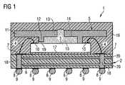
- the semiconductor package 1comprises a device carrier 2, a semiconductor die 3 which is electrically connected to the device carrier 2 by bond wires 4 and a heat spreader 5 which is mounted on the upper active surface of the die 3.
- the device carrier 2comprises an insulation carrier 6, multilayer copper distribution traces 20, a plurality of contact areas 7 on its upper surface, a plurality of via contacts 18, and a plurality of device contacts 8 on its bottom surface. Solder balls 9 are attached to the device contacts 8.
- the inner structure of the device carrier 2is illustrated in Fig. 1 by way of two via contacts 18 which connect a contact area 7 with a device contact 8.
- the die 3is mounted on the device carrier 2 and it has a plurality of die pads 10 located at the edges of its upper surface. Bond wires 4 between die pads 10 and the contact areas 7 electrically connect the die 3 to the device carrier 2.
- a copper heat spreader 5is mounted on the upper active surface of the die 3.
- the heat spreader 5includes an upper plate 11 and a foot ring 12 which protrudes from the bottom surface of the upper plate 11.
- the foot ring 12is integral with the upper plate 11.
- the upper plate 11is laterally larger than the width of the die 3 and includes an aperture 13 located in the centre of its lateral plane.
- the foot ring 12is located centrally around the longitudinal axis of the upper plate 11.
- the height of the foot ring 12is greater than the height of the bond wires 4 above the upper active surface of the die 3 and its width is smaller than the distance between the die pads 10 on opposing sides of the die 3.
- the heat spreader 5is positioned so that the foot ring 12 is mounted centrally on the upper surface of die 3 within the die pads 10. The bottom surface of the foot ring 12 is in partial contact with the upper surface of the die 3.
- the cavity 14 formed by the aperture 13, by the foot ring 12 and by the upper surface of the die 3is filled with adhesive material 15.
- the adhesive material 15is highly adhesive, has a low viscosity, is thermally conductive and includes at least in part electrically conductive material.
- the die 3, bond wires 4 and heat spreader 5are encapsulated by a plastic cover 16.
- the plate 11, foot ring 12 and aperture 13 which comprise the heat spreader 5are in this embodiment of the invention laterally square.
- the device carrier 2is replaced by a substrate which is known in the state of the art such as BT or leadframe.
- the diemay be any semiconductor device or plurality of devices but the invention is particularly advantageous for power devices which generate a lot of heat.
- the solder balls 9may be replaced by any suitable device contacting means, such as pins.
- the heatspreader 5may be made from any thermally conductive material such as Ag, Al or on of their alloys, a Cu-alloy. A metal/Invar type composite is also possible which also has the advantage in reducing the difference in thermal expansion properties between the die 3 and the heatspreader 5.
- the form of the upper plate 11 of the heatspreader 5is not important but may be a round disc, hexagonal disc etc and can be as large as necessary to dissipate the heat from a given die 3.
- the form of the foot ring 12can be chosen so that the contact area between the foot ring 12 and the heat producing areas of the die 3 is maximised. It is therefore clear that any lateral form of the heat spreader 5 and therefore cavity 14 is possible.
- the wires 4 making up the electrical connection between the die 3 and the device carrier 2may be replaced by other connecting means.
- the packagemay or may not be encapsulated and the top surface of the heatspreader may or may not be encapsulated.
- bond wires 4are attached between the die pads 10 and the contact areas 7 to electrically connect the die 3 with the device carrier 2.
- the heat spreader 5is then positioned on the upper active surface of the die 3 and the cavity 14 formed by the aperture 13, foot ring 12 and upper surface of the die 3 is filled with adhesive material 15.
- the gap 20 between the foot ring 12 and upper active surface of the die 3is filled with the adhesive material 15 which flows from the cavity 14. After the adhesive material is dispensed into the cavity 14, it is given an appropriate curing treatment to attach the heatpreader 5 to the die 3.
- the structure of the heatspreader 5assures that the adhesive material 15 is contained largely within the cavity 14 and does not spread onto the die pads 10 and wires 4. This enables the use of thermally conductive adhesive material which is also electrically conductive. Such adhesive material enables the more efficient dissipation of the heat generated by the active upper surface of the die 3.
- solder balls 9are attached to the device contacts 8 on the bottom surface of the device carrier 2.
- the solder balls 9enable the package to be mounted onto a circuit board (not shown) and the transfer of signals from external devices (also not shown).
- the encapsulation stepis omitted.
- the heat generated by the die 3is dissipated by conduction into the foot ring 12, into the adhesive material 15 and into the upper plate 11 of the heatspreader 5.
- the heatspreader 5provides an improved upward thermal conductive path as, firstly, there is a physical contact between the heatspreader 5 and the upper active surface of the die 3. Secondly, any gaps or imperfections in this interface are filled by the adhesive material 15. Thirdly, the adhesive material 15 contains at least in part metal particles providing the adhesive material with improved thermal conduction properties. The heat is then finally dissipated into the air by radiation from the heatspreader 5 and/or plastic cover.
Landscapes
- Physics & Mathematics (AREA)
- Condensed Matter Physics & Semiconductors (AREA)
- General Physics & Mathematics (AREA)
- Engineering & Computer Science (AREA)
- Computer Hardware Design (AREA)
- Microelectronics & Electronic Packaging (AREA)
- Power Engineering (AREA)
- Cooling Or The Like Of Semiconductors Or Solid State Devices (AREA)
Description
- The present invention relates to a structure of a semiconductor package.
- Fuelled by exponential increases in device clock speeds, the heat which must be dissipated in electronic devices has grown dramatically in recent years. Poor heat dissipation in packaged electronic devices limits device performance and the size of the module. In some cases, the need for an external heat sink to manage the thermal dissipation has limited the size of a small module or end-product which is not in tune with the key technology trend. Electronics gadgets are growing smaller in size so that ever smaller modules containing an ever increasing density of devices are desired.
- Heat dissipation is an increasing problem and improved thermal management is required. To date, this problem has not been satisfactorily solved to a extent particularly for simple low-cost heat dissipation.
- One solution is the cavity-down approach. However, the routing space for signals, powers and grounds traces is limited which results in lower I/Os. Also, the assembly processes are difficult with high material and packaging costs.
US 6 339 254 B1 discloses a stacked multi-chip assemblage including a plurality of integrated circuit die directly attached to a substrate having pads corresponding to terminals on the die and interconnections between the die, and also external contacts.US 5,681,663 discloses a heat spreader carrier strip including a first strip of laminated material portioned into smaller heat spreader portions with a welded second strip. Thermal manufacturing cycles will not cause a bowing of the second strip or of the heat spreader sections.US 5,156,923 discloses a heat transferring circuit substrate including layers of copper and Invar which has limited thermal expansion.US 5,358,795 discloses a heat-conductive material which receives and releases heat evenly, has excellent thermal conductivity and can have any desired thermal expansion coefficient.US 5,736,785 discloses a structure, shown in Figure 5a, where a planar heat spreader is mounted on the top surface of a semiconductor die, which in turn is mounted on and electrically connected to a substrate. The planar heat spreader comprises a central recessed portion protruding from the bottom surface of the heat spreader surrounded by a plurality of apertures at the edges. The die is coated with a layer of adhesive covering also the bonding wires attaching the die to the substrate. This structure has a limited thermal efficiency.JP 11 297 901 US 6,429,513 B1 discloses an active heat sink including a cavity partially filled with a heat activated liquid. The vapour condenses on an inner surface of the active heat sink and transfers heat to an outer, possibly finned, surface exposed to ambient to dissipate heat.US 5,349,237 discloses a plastic encapsulated integrated circuit with heat dissipating means in the form of a hermetically sealed container embedded in the package and extending from the integrated circuit to at least an outer surface of the package. A volatile liquid is disposed in the container.- It is one object of the present invention to provide a packaging structure offering an enhanced thermal management solution. The above and other objects are solved by the independent patent claims. Further improvements are given in the dependent patent claims.
- The invention provides an interface between the die and the heat spreader which is bridged in part by adhesive or solder.
- A fluid adhesive gives good physical connection between the die and heat spreader surfaces as a fluid compensates for surface imperfections. Even better thermal conductive properties are found in adhesives which are also at least partly electrically conductive as they contain metal particles. These cannot be used in the structure of
US 5,736,785 as the adhesive also covers the bonding wires and undesirable electrical shorts between the bonding wires and heat spreader will occur. - The present invention provides a semiconductor package comprising a device carrier having a plurality of contact areas, a semiconductor die having a plurality of die pads located at the edges of its active surface mounted to the device carrier, connection means to electrically connect the die pads on the die to the contact areas on the device carrier, a device contact means such as a solder ball array on the bottom side of the device carrier, and a heat spreading means which includes an upper plate and a foot ring which protrudes from a bottom surface of the upper plate and which is positioned between the die pads on the active surface such that a cavity is formed between the heat spreading means and the active surface, the cavity being filled with an adhering means interconnecting the heat spreading means and the active surface and methods of assembling such a package.
- It is advantageous to attach a heat spreading means to the upper surface of the die as heat is dissipated upwards away from the board so that neighbouring devices are not overheated. There is also easy routing of the wires making up the electrical connections and there is no need for an external heat sink so that the size of the package is not increased. Conventional adhesives and packaging technology can be used simplifying the processing route.
- A heat spreading means of high thermal conductivity preferably comprises a material selected from Cu, Al, Ag or an alloy of one of these, as these materials have good thermal conduction properties thus enabling efficient heat conduction away from the active surface. More preferably the heat spreading means comprises Cu as copper has good thermal conductivity, is readily available and is the least costly material. The heat spreading means is attached to the active surface of the die. The heat spreading means includes an upper plate and an integral foot ring protruding from the bottom surface.
- The heat spreading means preferably includes an aperture located in the upper plate, the aperture extending between the cavity and the upper surface of the upper plate. This enables the cavity to be filled with adhesive material or other adhering means from above after the heat spreader has been placed onto the die.
- The upper plate of the heat spreading means is preferably laterally square so as to be compatible with the existing assembly line and is preferably laterally larger than the width of the die in order to increase heat dissipation.
- Preferably the foot ring is laterally square, so as to have the greatest contact area with the die has a height greater than the height of the connecting means above the upper surface of the die so that the upper plate section of the heat spreading means is not in contact with the connecting means and electrical shorting does not occur. The width of the foot ring smaller than the distance between the die pads on opposing sides of the die again so that undesirable electrical contact is not made between the heat spreader and connecting means.
- The at least partial direct contact between the heat spreading means and the active surface of the die facilitates the dissipation of heat through a small number of layers thereby enhancing heat dissipation.
- Preferably the adhering means is a thermally conductive adhesive such as epoxy glue, sealant resin, thermal grease or liquid encapsulant in order to improve heat dissipation from the die to the heat spreading means. Preferably the adhesive material includes at least in part electrically conductive material as such adhesive has a high thermal conductivity.
- The structure of a heat spreading means allows control of the adhesive means as the adhesive means is contained within the cavity and does not spread into surrounding area, in particular onto the connecting means. This enables the use of electrically conductive adhesive which has superior thermal conduction properties, thereby enabling improved heat dissipation.
- The present invention also relates to methods of mounting a semiconductor package.
- A method comprises the steps of attaching a semiconductor die, which has a plurality of die pads on its active surface, to a device carrier such as BT or lead frame having contact areas by, for example, a die attach process. Electrical connections between the die and the substrate are made by, for example, attaching bond wires between the die pads and conductive traces on the substrate. Next, a heat spreading means, which includes an upper plate and foot ring which protrudes from a bottom surface of the upper plate, is positioned between the die pads on the active surface of the die such that a cavity is formed between the heat spreading means and the active surface. The cavity is then filled with adhering means such that the adhering means interconnects the heat spreading means and the active surface and curing the adhering means.
- Preferably the cavity is filled with an adhering means by dispensing adhesive through an aperture located in the heat spreading means as this enables the adhesive to enter the cavity from above. The spread of the adhesive to be contained largely within the cavity.
- A further method comprises the steps of attaching a semiconductor die, which has a plurality of die pads on its active surface and special contact areas for the solder adhering means, to a device carrier having a plurality of contact areas. Electrical connections are then made between the die and the substrate. Next, a heat spreading means, which includes an upper plate and foot ring which protrudes from a bottom surface of the upper plate, is positioned between the die pads on the active surface such that a cavity is formed between the heat spreading means and the active surface. The cavity is then filled with solder means and the semiconductor package heated such that the solder means interconnects the heat spreading means and the active surface.
- If a solder means is used for adhering the heat spreader to the active surface of the die, the semiconductor die may be provided with special contact areas for the solder on its active surface. Solder means has good thermal conductivity and the foot ring stops the solder from spreading onto the die pads and bond wires so that shorting between the device and heat spreader is prevented.
- There are two methods for mounting the embodiment which includes solder adhering means. The solder means may be spread onto the surface of the die within the die pads before the heat spreader is positioned on the surface of the die. The solder and heat spreader are so positioned that the solder is contained within the foot ring of the heat spreading means. In this embodiment it is not necessary for the heat spreader to contain an aperture in the upper plate. The package is then heated so that the solder interconnects the foot ring and therefore the heat spreader with the active surface of the die.
- Alternatively, the heat spreader is positioned on the die and the solder means dispensed through the aperture in the upper plate. The semiconductor package is then heated so that the solder means interconnects the heat spreading means and the active surface.
- One further advantage of the present invention is that it offers a simple low-cost solution for enhanced thermal management whereby the current conventional assembly packaging technology of a laminate package can still be used. The invention can be used for all existing semiconductor devices. It eliminates the need for an external heat sink which doubles or triples the size (in terms of thickness) of the package or component. This affects the overall dimension of the modules or application boards. The present invention also enables improved trace routability over the existing cavity-down thermal management solutions.
- The invention favours heat dissipation upwards from the active surface which means that heat is dissipated away from the board. This is highly desirable as heat dissipation path along the device carrier could overheat the adjacent components when mounted onto the application board.
- One concept of this invention includes an integrated circuit device whereby the heat spreader, which can be a composite of either Cu, Cu alloys, Al, Al alloys, Ag and Ag alloys is mounted onto this device using thermally conductive adhesives such as epoxy glue, sealant resins, thermal grease or even liquid encapsulant. Some of these adhesives can also be used to attach devices to a carrier such as a BT substrate or lead frame in the die attach process. Packaging of stack-die has also used such adhesives when attaching two devices together stacking them one on top of the other. One embodiment of the invention would be the use of selected material i.e. pure copper (Cu) for the heat spreader and an epoxy glue formulated with high adhesive and low viscosity properties as the thermally conductive adhesives to attach the heat spreader onto the die.
- A concept introduced in the present invention can also be seen in the design of the aperture in the heat spreading means. This acts as a funnel so that the adhesive can be filled-in through this funnel to make the attachment of the heat spreader onto the die top. The funnel-like design allows the adhesives to be contained within the boundary of the heat spreader inner-walls which controls creeping of adhesive preventing it from smudging the surface of the dies. Under such well-defined process control, the contact area between the heat spreader base and the die top surface could also be enlarged to have optimum adhesion between the heat spreader and the die top and in addition creates also an avenue for another heat transfer path. This approach of having a direct attachment of heat spreader onto die top surface by means of dispensing adhesives improves its thermal properties.
- The concept can be applied differently, e.g. by exposing the copper heat spreader or by burying the heat spreader by encapsulating it within the package. Both deliver the desired thermal dissipation except that the exposed heat spreader would have a better thermal dissipation performance. The design can be chosen to suit the kind of assembly process that has been established in the conventional platform of the process / production line.
- The invention can be easily seen by X-Ray on the package or assembled component. Conventional packaging technology can be used without having to change or introduce an entirely new assembly process line.
- An embodiment of the invention will now be described by way of example with reference to the drawings.
- Fig. 1
- shows a cross-sectional view of the structure of a semiconductor package according to the invention and
- Fig. 2
- shows a perspective and exploded view of the semiconductor package of
Fig. 1 . - The
semiconductor package 1 comprises adevice carrier 2, asemiconductor die 3 which is electrically connected to thedevice carrier 2 bybond wires 4 and a heat spreader 5 which is mounted on the upper active surface of thedie 3. - The
device carrier 2 comprises an insulation carrier 6, multilayer copper distribution traces 20, a plurality ofcontact areas 7 on its upper surface, a plurality of viacontacts 18, and a plurality ofdevice contacts 8 on its bottom surface.Solder balls 9 are attached to thedevice contacts 8. The inner structure of thedevice carrier 2 is illustrated inFig. 1 by way of two viacontacts 18 which connect acontact area 7 with adevice contact 8. - The
die 3 is mounted on thedevice carrier 2 and it has a plurality ofdie pads 10 located at the edges of its upper surface.Bond wires 4 between diepads 10 and thecontact areas 7 electrically connect thedie 3 to thedevice carrier 2. - A copper heat spreader 5 is mounted on the upper active surface of the
die 3. The heat spreader 5 includes anupper plate 11 and afoot ring 12 which protrudes from the bottom surface of theupper plate 11. Thefoot ring 12 is integral with theupper plate 11. Theupper plate 11 is laterally larger than the width of thedie 3 and includes anaperture 13 located in the centre of its lateral plane. Thefoot ring 12 is located centrally around the longitudinal axis of theupper plate 11. The height of thefoot ring 12 is greater than the height of thebond wires 4 above the upper active surface of thedie 3 and its width is smaller than the distance between thedie pads 10 on opposing sides of thedie 3. - The heat spreader 5 is positioned so that the
foot ring 12 is mounted centrally on the upper surface ofdie 3 within thedie pads 10. The bottom surface of thefoot ring 12 is in partial contact with the upper surface of thedie 3. - The
cavity 14 formed by theaperture 13, by thefoot ring 12 and by the upper surface of thedie 3 is filled withadhesive material 15. Theadhesive material 15 is highly adhesive, has a low viscosity, is thermally conductive and includes at least in part electrically conductive material. - As can be seen in
Fig 1 , but notFig. 2 , incomplete contact between the bottom surface of thefoot ring 12 and upper surface of thedie 3 results indiscrete gaps 19 in the interface. These gaps are filled with theadhesive material 15. - The
die 3,bond wires 4 and heat spreader 5 are encapsulated by aplastic cover 16. - As can be best seen in
Fig. 2 , theplate 11,foot ring 12 andaperture 13 which comprise the heat spreader 5 are in this embodiment of the invention laterally square. - There are many possible alternatives to the embodiment shown in the figures. In an embodiment not shown in the figures, the
device carrier 2 is replaced by a substrate which is known in the state of the art such as BT or leadframe. The die may be any semiconductor device or plurality of devices but the invention is particularly advantageous for power devices which generate a lot of heat. Thesolder balls 9 may be replaced by any suitable device contacting means, such as pins. - The heatspreader 5 may be made from any thermally conductive material such as Ag, Al or on of their alloys, a Cu-alloy. A metal/Invar type composite is also possible which also has the advantage in reducing the difference in thermal expansion properties between the
die 3 and the heatspreader 5. The form of theupper plate 11 of the heatspreader 5 is not important but may be a round disc, hexagonal disc etc and can be as large as necessary to dissipate the heat from a givendie 3. The form of thefoot ring 12 can be chosen so that the contact area between thefoot ring 12 and the heat producing areas of thedie 3 is maximised. It is therefore clear that any lateral form of the heat spreader 5 and thereforecavity 14 is possible. Thewires 4 making up the electrical connection between thedie 3 and thedevice carrier 2 may be replaced by other connecting means. The package may or may not be encapsulated and the top surface of the heatspreader may or may not be encapsulated. - The steps in the method to assemble semiconductor package are as follows:
- After the attachment of a
die 3 to adevice carrier 2 using die attachmaterial 17,bond wires 4 are attached between thedie pads 10 and thecontact areas 7 to electrically connect thedie 3 with thedevice carrier 2. - The heat spreader 5 is then positioned on the upper active surface of the
die 3 and thecavity 14 formed by theaperture 13,foot ring 12 and upper surface of thedie 3 is filled withadhesive material 15. Thegap 20 between thefoot ring 12 and upper active surface of thedie 3 is filled with theadhesive material 15 which flows from thecavity 14. After the adhesive material is dispensed into thecavity 14, it is given an appropriate curing treatment to attach the heatpreader 5 to thedie 3. - The structure of the heatspreader 5 assures that the
adhesive material 15 is contained largely within thecavity 14 and does not spread onto thedie pads 10 andwires 4. This enables the use of thermally conductive adhesive material which is also electrically conductive. Such adhesive material enables the more efficient dissipation of the heat generated by the active upper surface of thedie 3. - The package is then encapsulated by a molding process and
solder balls 9 are attached to thedevice contacts 8 on the bottom surface of thedevice carrier 2. Thesolder balls 9 enable the package to be mounted onto a circuit board (not shown) and the transfer of signals from external devices (also not shown). - In an alternative embodiment of the invention the encapsulation step is omitted.
- The heat generated by the
die 3 is dissipated by conduction into thefoot ring 12, into theadhesive material 15 and into theupper plate 11 of the heatspreader 5. The heatspreader 5 provides an improved upward thermal conductive path as, firstly, there is a physical contact between the heatspreader 5 and the upper active surface of thedie 3. Secondly, any gaps or imperfections in this interface are filled by theadhesive material 15. Thirdly, theadhesive material 15 contains at least in part metal particles providing the adhesive material with improved thermal conduction properties. The heat is then finally dissipated into the air by radiation from the heatspreader 5 and/or plastic cover. - 1
- semiconductor package
- 2
- device carrier
- 3
- semiconductor die
- 4
- bond wire
- 5
- heat spreader
- 6
- insulation carrier
- 7
- contact area
- 8
- device contact
- 9
- solder ball
- 10
- die pad
- 11
- upper plate
- 12
- foot ring
- 13
- aperture
- 14
- cavity
- 15
- adhesive material
- 16
- plastic cover
- 17
- die attach material
- 18
- via contact
- 19
- gap
- 20
- distribution trace
Claims (11)
- A semiconductor package (1) comprising the following features:- a device carrier (2) having a plurality of contact areas (7),- a semiconductor die (3) having a plurality of die pads (10) on an active surface, the semiconductor die (3) being mounted on the device carrier (2),- connection means (4) to electrically connect the die pads (10) to the contact areas (7),- a heat spreading means (5) mounted on the active surface of the die (3),wherein the heat spreading means includes an upper plate (11) and a foot ring (12) which protrudes from a bottom surface of the upper plate (11) and which is positioned between the die pads (10) on the active surface such that a cavity (14) is formed between the heat spreading means (5) and the active surface of the die (3), confined by the foot ring (12), the cavity being filled with an adhering means (15) interconnecting the heat spreading means (5) and the active surface,
characterized in that
the heat spreading means (5) includes an aperture (13), the aperture (13) being a through-hole in the upper plate (11) of the heat spreading means (5), the aperture (13) extending between the cavity (14) and the upper surface of the upper plate (11). - A semiconductor package (1) according to claim 1,
characterized in that
the adhering means comprises an adhesive (15) and/or a solder. - A semiconductor package (1) according to claim 2,
characterized in that
the adhesive material is a thermally conductive adhesive such as epoxy glue, sealant resin, thermal grease or liquid encapsulant. - A semiconductor package (1) according to claim 2 or claim 3,
characterized in that
the adhesive material (15) comprises electrically conductive material. - A semiconductor package (1) according to one of the aforementioned claims,
characterized in that
the upper plate (11) of the heat spreading means (5) and/or the foot ring (12) are laterally square. - A semiconductor package (1) according to one of the aforementioned claims,
characterized in that
the upper plate (11) of the heat spreading means (5) is laterally larger than the width of the die (3). - A semiconductor package (1) according to one of the aforementioned claims,
characterized in that
the height of the foot ring (12) is greater than the height of the connection means (4) above the upper surface of the die (3). - A method to mount a semiconductor package (1) comprising the following steps:- providing a device carrier (2) having a plurality of contact areas (7),- attaching a semiconductor die (3) on the device carrier (2), the semiconductor die (3) having a plurality of die pads (10) on an active surface,- making electrical connections between the die pads (10) and the contact areas (7) using connection means (4),- placing a heat spreading means (5) on the active surface of the die (3), the heat spreading means (5) including an upper plate (11) and a foot ring (12) which protrudes from a bottom surface of the upper plate (11) and which is positioned between the die pads (10) on the active surface such that a cavity (14) is formed between the heat spreading means (5) and the active surface of the die (3), confined by the foot ring (12),- dispensing adhesive means through an aperture (13) located in the upper plate (11) of the heat spreading means (5), the aperture (13) being a through-hole in the upper plate (11) of the heat spreading means (5), and to fill the cavity (14) with the adhesive means (15) such that the adhesive means (15) interconnects the heat spreading means (5) and the active surface,- curing the adhering means (15).
- A method to mount a semiconductor package (1) comprising the following steps:- providing a device carrier (2) having a plurality of contact areas (7),- attaching a semiconductor die (3) on the device carrier (2), the semiconductor die (3) having a plurality of die pads (10) on an active surface,- making electrical connections between the die pads (10) and the contact areas (7) using connection means (4),- placing a heat spreading means (5) on the active surface of the die (3), the heat spreading means (5) including an upper plate (11) and a foot ring (12) which protrudes from a bottom surface of the upper plate (11), the foot ring being positioned between the die pads (10) on the active surface such that a cavity (14) is formed between the heat spreading means (5) and the active surface of the die (3), confined by the foot ring (12), the cavity (14) containing a solder means,- heating the semiconductor package (1) such that the solder means interconnects the heat spreading means (5) and the active surface.
- A method to mount a semiconductor package (1) according to claim 9,
characterized in that
the upper plate (11) comprises an aperture (13), the heat spreading means (5) is positioned on the die (3) and solder is dispensed through the aperture (13) to fill the cavity (14). - A method to mount a semiconductor package (1) according to claim 9,
characterized in that
the solder is positioned on the active surface of the die (3) so that the solder is contained within the foot ring (12) of the heat spreader (5) when the heat spreading means (5) is subsequently positioned on the die (3).
Priority Applications (4)
| Application Number | Priority Date | Filing Date | Title |
|---|---|---|---|
| DE60326587TDE60326587D1 (en) | 2003-10-13 | 2003-10-13 | Semiconductor housing with heat spreader |
| EP03023225AEP1524690B1 (en) | 2003-10-13 | 2003-10-13 | Semiconductor package with heat spreader |
| SG200405924ASG111226A1 (en) | 2003-10-13 | 2004-10-11 | Semiconductor package with heat spreader |
| US10/963,280US7196403B2 (en) | 2003-10-13 | 2004-10-12 | Semiconductor package with heat spreader |
Applications Claiming Priority (1)
| Application Number | Priority Date | Filing Date | Title |
|---|---|---|---|
| EP03023225AEP1524690B1 (en) | 2003-10-13 | 2003-10-13 | Semiconductor package with heat spreader |
Publications (2)
| Publication Number | Publication Date |
|---|---|
| EP1524690A1 EP1524690A1 (en) | 2005-04-20 |
| EP1524690B1true EP1524690B1 (en) | 2009-03-11 |
Family
ID=34354451
Family Applications (1)
| Application Number | Title | Priority Date | Filing Date |
|---|---|---|---|
| EP03023225AExpired - LifetimeEP1524690B1 (en) | 2003-10-13 | 2003-10-13 | Semiconductor package with heat spreader |
Country Status (4)
| Country | Link |
|---|---|
| US (1) | US7196403B2 (en) |
| EP (1) | EP1524690B1 (en) |
| DE (1) | DE60326587D1 (en) |
| SG (1) | SG111226A1 (en) |
Families Citing this family (57)
| Publication number | Priority date | Publication date | Assignee | Title |
|---|---|---|---|---|
| US7182498B2 (en)* | 2004-06-30 | 2007-02-27 | 3M Innovative Properties Company | Phosphor based illumination system having a plurality of light guides and an interference reflector |
| US20060060952A1 (en)* | 2004-09-22 | 2006-03-23 | Tsorng-Dih Yuan | Heat spreader for non-uniform power dissipation |
| US7355276B1 (en)* | 2005-03-11 | 2008-04-08 | Maxtor Corporation | Thermally-enhanced circuit assembly |
| DE102005014674B4 (en) | 2005-03-29 | 2010-02-11 | Infineon Technologies Ag | Semiconductor module with semiconductor chips in a plastic housing in separate areas and method for producing the same |
| DE102005054268B4 (en)* | 2005-11-11 | 2012-04-26 | Infineon Technologies Ag | Method for producing a semiconductor device with at least one semiconductor chip |
| TWI291752B (en)* | 2006-02-27 | 2007-12-21 | Siliconware Precision Industries Co Ltd | Semiconductor package with heat dissipating device and fabrication method thereof |
| US8115301B2 (en)* | 2006-11-17 | 2012-02-14 | Stats Chippac, Inc. | Methods for manufacturing thermally enhanced flip-chip ball grid arrays |
| US9018667B2 (en)* | 2008-03-25 | 2015-04-28 | Bridge Semiconductor Corporation | Semiconductor chip assembly with post/base heat spreader and dual adhesives |
| US8232576B1 (en) | 2008-03-25 | 2012-07-31 | Bridge Semiconductor Corporation | Semiconductor chip assembly with post/base heat spreader and ceramic block in post |
| US8525214B2 (en) | 2008-03-25 | 2013-09-03 | Bridge Semiconductor Corporation | Semiconductor chip assembly with post/base heat spreader with thermal via |
| US8531024B2 (en)* | 2008-03-25 | 2013-09-10 | Bridge Semiconductor Corporation | Semiconductor chip assembly with post/base heat spreader and multilevel conductive trace |
| US20100181594A1 (en)* | 2008-03-25 | 2010-07-22 | Lin Charles W C | Semiconductor chip assembly with post/base heat spreader and cavity over post |
| US8354688B2 (en) | 2008-03-25 | 2013-01-15 | Bridge Semiconductor Corporation | Semiconductor chip assembly with bump/base/ledge heat spreader, dual adhesives and cavity in bump |
| US8324723B2 (en)* | 2008-03-25 | 2012-12-04 | Bridge Semiconductor Corporation | Semiconductor chip assembly with bump/base heat spreader and dual-angle cavity in bump |
| US8288792B2 (en)* | 2008-03-25 | 2012-10-16 | Bridge Semiconductor Corporation | Semiconductor chip assembly with post/base/post heat spreader |
| US8203167B2 (en)* | 2008-03-25 | 2012-06-19 | Bridge Semiconductor Corporation | Semiconductor chip assembly with post/base heat spreader and adhesive between base and terminal |
| US8378372B2 (en)* | 2008-03-25 | 2013-02-19 | Bridge Semiconductor Corporation | Semiconductor chip assembly with post/base heat spreader and horizontal signal routing |
| US8314438B2 (en)* | 2008-03-25 | 2012-11-20 | Bridge Semiconductor Corporation | Semiconductor chip assembly with bump/base heat spreader and cavity in bump |
| US20100072511A1 (en)* | 2008-03-25 | 2010-03-25 | Lin Charles W C | Semiconductor chip assembly with copper/aluminum post/base heat spreader |
| US8148747B2 (en)* | 2008-03-25 | 2012-04-03 | Bridge Semiconductor Corporation | Semiconductor chip assembly with post/base/cap heat spreader |
| US8212279B2 (en)* | 2008-03-25 | 2012-07-03 | Bridge Semiconductor Corporation | Semiconductor chip assembly with post/base heat spreader, signal post and cavity |
| US20090284932A1 (en)* | 2008-03-25 | 2009-11-19 | Bridge Semiconductor Corporation | Thermally Enhanced Package with Embedded Metal Slug and Patterned Circuitry |
| US8310043B2 (en)* | 2008-03-25 | 2012-11-13 | Bridge Semiconductor Corporation | Semiconductor chip assembly with post/base heat spreader with ESD protection layer |
| US7948076B2 (en)* | 2008-03-25 | 2011-05-24 | Bridge Semiconductor Corporation | Semiconductor chip assembly with post/base heat spreader and vertical signal routing |
| US8415703B2 (en)* | 2008-03-25 | 2013-04-09 | Bridge Semiconductor Corporation | Semiconductor chip assembly with post/base/flange heat spreader and cavity in flange |
| US8193556B2 (en)* | 2008-03-25 | 2012-06-05 | Bridge Semiconductor Corporation | Semiconductor chip assembly with post/base heat spreader and cavity in post |
| US8067784B2 (en)* | 2008-03-25 | 2011-11-29 | Bridge Semiconductor Corporation | Semiconductor chip assembly with post/base heat spreader and substrate |
| US8129742B2 (en) | 2008-03-25 | 2012-03-06 | Bridge Semiconductor Corporation | Semiconductor chip assembly with post/base heat spreader and plated through-hole |
| US8329510B2 (en)* | 2008-03-25 | 2012-12-11 | Bridge Semiconductor Corporation | Method of making a semiconductor chip assembly with a post/base heat spreader with an ESD protection layer |
| US8207553B2 (en)* | 2008-03-25 | 2012-06-26 | Bridge Semiconductor Corporation | Semiconductor chip assembly with base heat spreader and cavity in base |
| US20110278638A1 (en) | 2008-03-25 | 2011-11-17 | Lin Charles W C | Semiconductor chip assembly with post/dielectric/post heat spreader |
| US20110163348A1 (en)* | 2008-03-25 | 2011-07-07 | Bridge Semiconductor Corporation | Semiconductor chip assembly with bump/base heat spreader and inverted cavity in bump |
| US20110156090A1 (en)* | 2008-03-25 | 2011-06-30 | Lin Charles W C | Semiconductor chip assembly with post/base/post heat spreader and asymmetric posts |
| US20100052005A1 (en)* | 2008-03-25 | 2010-03-04 | Lin Charles W C | Semiconductor chip assembly with post/base heat spreader and conductive trace |
| US8269336B2 (en)* | 2008-03-25 | 2012-09-18 | Bridge Semiconductor Corporation | Semiconductor chip assembly with post/base heat spreader and signal post |
| US9070662B2 (en)* | 2009-03-05 | 2015-06-30 | Volterra Semiconductor Corporation | Chip-scale packaging with protective heat spreader |
| US7964951B2 (en)* | 2009-03-16 | 2011-06-21 | Ati Technologies Ulc | Multi-die semiconductor package with heat spreader |
| US8039316B2 (en)* | 2009-04-14 | 2011-10-18 | Stats Chippac Ltd. | Integrated circuit packaging system with stacked integrated circuit and heat spreader with openings and method of manufacture thereof |
| US8384228B1 (en) | 2009-04-29 | 2013-02-26 | Triquint Semiconductor, Inc. | Package including wires contacting lead frame edge |
| US8324653B1 (en) | 2009-08-06 | 2012-12-04 | Bridge Semiconductor Corporation | Semiconductor chip assembly with ceramic/metal substrate |
| US8299482B2 (en)* | 2009-10-05 | 2012-10-30 | Intellectual Discovery Co., Ltd. | Light emitter |
| CN102792441B (en)* | 2010-03-12 | 2016-07-27 | 富士通株式会社 | Radiator structure and manufacture method thereof |
| CN102569594A (en)* | 2010-12-24 | 2012-07-11 | 展晶科技(深圳)有限公司 | Package carrier and light emitting diode package structure using same |
| US8836110B2 (en) | 2012-08-31 | 2014-09-16 | Freescale Semiconductor, Inc. | Heat spreader for use within a packaged semiconductor device |
| US9111878B2 (en)* | 2013-01-31 | 2015-08-18 | Freescale Semiconductor, Inc | Method for forming a semiconductor device assembly having a heat spreader |
| US9961798B2 (en)* | 2013-04-04 | 2018-05-01 | Infineon Technologies Austria Ag | Package and a method of manufacturing the same |
| KR102127772B1 (en)* | 2013-05-16 | 2020-06-29 | 삼성전자주식회사 | Semiconductor package having heat spreader and method of forming the same |
| KR101994727B1 (en)* | 2013-12-18 | 2019-07-01 | 삼성전기주식회사 | Power module Package and Manufacturing Method for the same |
| JP6386746B2 (en) | 2014-02-26 | 2018-09-05 | 株式会社ジェイデバイス | Semiconductor device |
| DE102014118080B4 (en)* | 2014-12-08 | 2020-10-15 | Infineon Technologies Ag | Electronic module with a heat spreader and method of making it |
| JP6382784B2 (en)* | 2015-11-26 | 2018-08-29 | 株式会社Soken | Manufacturing method of semiconductor device |
| JP6897141B2 (en)* | 2017-02-15 | 2021-06-30 | 株式会社デンソー | Semiconductor devices and their manufacturing methods |
| JP6867245B2 (en) | 2017-06-28 | 2021-04-28 | 日立Astemo株式会社 | Electric drive device and electric power steering device |
| US20190214328A1 (en)* | 2018-01-10 | 2019-07-11 | Feras Eid | Stacked die architectures with improved thermal management |
| JP7414822B2 (en)* | 2019-01-22 | 2024-01-16 | 長江存儲科技有限責任公司 | Integrated circuit packaging structure and manufacturing method thereof |
| CN114944375B (en)* | 2022-05-23 | 2022-10-28 | 山东中清智能科技股份有限公司 | Power device packaging structure and preparation method thereof |
| CN116613110B (en)* | 2023-06-16 | 2024-02-23 | 广东气派科技有限公司 | Preparation method of cover plate packaging structure for enhancing heat dissipation and cover plate packaging structure |
Family Cites Families (15)
| Publication number | Priority date | Publication date | Assignee | Title |
|---|---|---|---|---|
| EP0537965B1 (en)* | 1991-10-12 | 1997-03-05 | Sumitomo Special Metals Company Limited | Process of manufacturing a heat-conductive material |
| US5156923A (en)* | 1992-01-06 | 1992-10-20 | Texas Instruments Incorporated | Heat-transferring circuit substrate with limited thermal expansion and method for making |
| US5349237A (en)* | 1992-03-20 | 1994-09-20 | Vlsi Technology, Inc. | Integrated circuit package including a heat pipe |
| US5681663A (en)* | 1995-06-09 | 1997-10-28 | Ford Motor Company | Heatspreader carrier strip |
| JPH09260555A (en)* | 1996-03-19 | 1997-10-03 | Mitsubishi Electric Corp | Semiconductor device |
| US5736785A (en)* | 1996-12-20 | 1998-04-07 | Industrial Technology Research Institute | Semiconductor package for improving the capability of spreading heat |
| JPH11297901A (en)* | 1998-04-14 | 1999-10-29 | Hitachi Ltd | Semiconductor device and manufacturing method thereof |
| SG75873A1 (en)* | 1998-09-01 | 2000-10-24 | Texas Instr Singapore Pte Ltd | Stacked flip-chip integrated circuit assemblage |
| US6570764B2 (en)* | 1999-12-29 | 2003-05-27 | Intel Corporation | Low thermal resistance interface for attachment of thermal materials to a processor die |
| KR20020086587A (en)* | 2000-03-09 | 2002-11-18 | 후지쯔 가부시끼가이샤 | Semiconductor device, method of manufacturing semiconductor device, lead frame, method of manufacturing lead frame, and method of manufacturing semiconductor device with lead frame |
| US6429513B1 (en)* | 2001-05-25 | 2002-08-06 | Amkor Technology, Inc. | Active heat sink for cooling a semiconductor chip |
| US6472741B1 (en)* | 2001-07-14 | 2002-10-29 | Siliconware Precision Industries Co., Ltd. | Thermally-enhanced stacked-die ball grid array semiconductor package and method of fabricating the same |
| TW498516B (en)* | 2001-08-08 | 2002-08-11 | Siliconware Precision Industries Co Ltd | Manufacturing method for semiconductor package with heat sink |
| TW552689B (en)* | 2001-12-21 | 2003-09-11 | Siliconware Precision Industries Co Ltd | High electrical characteristic and high heat dissipating BGA package and its process |
| US20050093135A1 (en)* | 2003-10-31 | 2005-05-05 | Wei-Chi Liu | Thermal dissipating element of a chip |
- 2003
- 2003-10-13EPEP03023225Apatent/EP1524690B1/ennot_activeExpired - Lifetime
- 2003-10-13DEDE60326587Tpatent/DE60326587D1/ennot_activeExpired - Lifetime
- 2004
- 2004-10-11SGSG200405924Apatent/SG111226A1/enunknown
- 2004-10-12USUS10/963,280patent/US7196403B2/ennot_activeExpired - Fee Related
Also Published As
| Publication number | Publication date |
|---|---|
| SG111226A1 (en) | 2005-05-30 |
| EP1524690A1 (en) | 2005-04-20 |
| US7196403B2 (en) | 2007-03-27 |
| DE60326587D1 (en) | 2009-04-23 |
| US20050116335A1 (en) | 2005-06-02 |
Similar Documents
| Publication | Publication Date | Title |
|---|---|---|
| EP1524690B1 (en) | Semiconductor package with heat spreader | |
| EP1256980B1 (en) | Ball grid array package with a heat spreader and method for making the same | |
| KR101634067B1 (en) | Semiconductor package and method of manufacturing the same | |
| US5986885A (en) | Semiconductor package with internal heatsink and assembly method | |
| US6790710B2 (en) | Method of manufacturing an integrated circuit package | |
| EP1374305B1 (en) | Enhanced die-down ball grid array and method for making the same | |
| US7138706B2 (en) | Semiconductor device and method for manufacturing the same | |
| US6429513B1 (en) | Active heat sink for cooling a semiconductor chip | |
| US8916958B2 (en) | Semiconductor package with multiple chips and substrate in metal cap | |
| US20100025810A1 (en) | Method and System for Secure Heat Sink Attachment on Semiconductor Devices with Macroscopic Uneven Surface Features | |
| US20020177258A1 (en) | Chip on board and heat sink attachment methods | |
| CA2676495C (en) | Mechanical barrier element for improved thermal reliability of electronic components | |
| US6614660B1 (en) | Thermally enhanced IC chip package | |
| US20070205495A1 (en) | Electronic Component With Stacked Semiconductor Chips And Heat Dissipating Means | |
| WO2003083956A9 (en) | Enhanced thermal dissipation integrated circuit package and method of manufacturing enhanced thermal dissipation integrated circuit package | |
| KR100698526B1 (en) | A wiring board having a heat dissipation layer and a semiconductor package using the same | |
| US7692276B2 (en) | Thermally enhanced ball grid array package formed in strip with one-piece die-attached exposed heat spreader | |
| JP4075204B2 (en) | Multilayer semiconductor device | |
| US6559537B1 (en) | Ball grid array packages with thermally conductive containers | |
| JP2019071412A (en) | Chip package | |
| KR20170093277A (en) | Sensor package and method of manufacturinng the same | |
| US7224058B2 (en) | Integrated circuit package employing a heat-spreader member | |
| CN1437233A (en) | Packaged semiconductor device and method of forming the same | |
| US20040217451A1 (en) | Semiconductor packaging structure | |
| KR20180004062A (en) | Sensor package and method of manufacturinng the same |
Legal Events
| Date | Code | Title | Description |
|---|---|---|---|
| PUAI | Public reference made under article 153(3) epc to a published international application that has entered the european phase | Free format text:ORIGINAL CODE: 0009012 | |
| AK | Designated contracting states | Kind code of ref document:A1 Designated state(s):AT BE BG CH CY CZ DE DK EE ES FI FR GB GR HU IE IT LI LU MC NL PT RO SE SI SK TR | |
| AX | Request for extension of the european patent | Extension state:AL LT LV MK | |
| 17P | Request for examination filed | Effective date:20050518 | |
| AKX | Designation fees paid | Designated state(s):DE | |
| 17Q | First examination report despatched | Effective date:20051124 | |
| GRAP | Despatch of communication of intention to grant a patent | Free format text:ORIGINAL CODE: EPIDOSNIGR1 | |
| GRAS | Grant fee paid | Free format text:ORIGINAL CODE: EPIDOSNIGR3 | |
| GRAA | (expected) grant | Free format text:ORIGINAL CODE: 0009210 | |
| AK | Designated contracting states | Kind code of ref document:B1 Designated state(s):DE | |
| REF | Corresponds to: | Ref document number:60326587 Country of ref document:DE Date of ref document:20090423 Kind code of ref document:P | |
| PLBE | No opposition filed within time limit | Free format text:ORIGINAL CODE: 0009261 | |
| STAA | Information on the status of an ep patent application or granted ep patent | Free format text:STATUS: NO OPPOSITION FILED WITHIN TIME LIMIT | |
| 26N | No opposition filed | Effective date:20091214 | |
| PGFP | Annual fee paid to national office [announced via postgrant information from national office to epo] | Ref country code:DE Payment date:20161220 Year of fee payment:14 | |
| REG | Reference to a national code | Ref country code:DE Ref legal event code:R119 Ref document number:60326587 Country of ref document:DE | |
| PG25 | Lapsed in a contracting state [announced via postgrant information from national office to epo] | Ref country code:DE Free format text:LAPSE BECAUSE OF NON-PAYMENT OF DUE FEES Effective date:20180501 |