EP1522879B2 - Opto-electronic sensor and method of detecting an object in a surveillance area - Google Patents
Opto-electronic sensor and method of detecting an object in a surveillance areaDownload PDFInfo
- Publication number
- EP1522879B2 EP1522879B2EP04023748.9AEP04023748AEP1522879B2EP 1522879 B2EP1522879 B2EP 1522879B2EP 04023748 AEP04023748 AEP 04023748AEP 1522879 B2EP1522879 B2EP 1522879B2
- Authority
- EP
- European Patent Office
- Prior art keywords
- optoelectronic sensor
- optical
- frequency
- optoelectronic
- light
- Prior art date
- Legal status (The legal status is an assumption and is not a legal conclusion. Google has not performed a legal analysis and makes no representation as to the accuracy of the status listed.)
- Expired - Lifetime
Links
- 230000005693optoelectronicsEffects0.000titleclaimsdescription87
- 238000000034methodMethods0.000titleclaimsdescription21
- 230000005540biological transmissionEffects0.000claimsdescription49
- 230000003287optical effectEffects0.000claimsdescription45
- 230000004888barrier functionEffects0.000claimsdescription20
- 238000011156evaluationMethods0.000claimsdescription12
- 238000000926separation methodMethods0.000claimsdescription12
- 238000006243chemical reactionMethods0.000claimsdescription4
- 239000003990capacitorSubstances0.000claimsdescription3
- 238000003860storageMethods0.000claimsdescription3
- 238000005070samplingMethods0.000description14
- 230000011514reflexEffects0.000description11
- 238000012544monitoring processMethods0.000description5
- 238000005259measurementMethods0.000description3
- 230000002123temporal effectEffects0.000description3
- 238000001514detection methodMethods0.000description2
- 238000010586diagramMethods0.000description2
- 230000005855radiationEffects0.000description2
- 230000000903blocking effectEffects0.000description1
- 230000001419dependent effectEffects0.000description1
- 238000013461designMethods0.000description1
- 238000009826distributionMethods0.000description1
- 238000009434installationMethods0.000description1
- 238000004519manufacturing processMethods0.000description1
- 239000002184metalSubstances0.000description1
- 230000003071parasitic effectEffects0.000description1
- 230000010287polarizationEffects0.000description1
- 238000012545processingMethods0.000description1
- 239000000523sampleSubstances0.000description1
- 239000007787solidSubstances0.000description1
Images


Classifications
- G—PHYSICS
- G01—MEASURING; TESTING
- G01V—GEOPHYSICS; GRAVITATIONAL MEASUREMENTS; DETECTING MASSES OR OBJECTS; TAGS
- G01V8/00—Prospecting or detecting by optical means
- G01V8/10—Detecting, e.g. by using light barriers
- G01V8/12—Detecting, e.g. by using light barriers using one transmitter and one receiver
- G01V8/14—Detecting, e.g. by using light barriers using one transmitter and one receiver using reflectors
Definitions
- the inventionrelates to an optoelectronic sensor, in particular a reflex light barrier or a diffuse reflection sensor, for detecting an object in a surveillance area, with a housing, with a transmitting and receiving optics, with at least one optoelectronic component and with an evaluation circuit.
- the inventionalso relates to a method for detecting an object in a surveillance area, with an optoelectronic sensor, wherein an electrical transmission signal is converted into an optical transmission signal, the optical transmission signal emitted in the surveillance area, from a reflector or an object as an optical reception signal at least partially reflected back to the optoelectronic sensor and converted into an electrical received signal
- Known optoelectronic sensorsalways have a light transmitter and at least one light receiver, d. H. at least two different optoelectronic components.
- transmission componentsie as light-emitting components, typically diodes, preferably laser diodes, and as receiving devices in general photodiodes.
- Optoelectronic sensorscan be divided essentially into three different types, namely disposable systems, reflection systems and stylus systems.
- One-way systemsconsist on the one hand of a transmitter device and on the other hand of a spatially separated from this receiver device.
- the transmitter device and the receiver deviceare disposed opposite to each other at the lateral boundaries of a region to be monitored, so that light emitted from the transmitter device can be received by the receiver device.
- the disadvantage hereis that two electronic devices needed to be mounted and supplied with electrical energy.
- reflection systemswhich are also referred to as reflex light barriers, transmitter and receiver are integrated in a single unit, ie in a single device.
- Such a transmitter / receiver device performing assemblyis arranged at an outer boundary of the area to be monitored, while at the other, this opposite boundary of the area to be monitored, a reflector, for. B. a triple mirror is provided, the light emitted by the transceiver device reflects back to it in such a way that it can be received by the receiver integrated in the transceiver device.
- the reflex light barrierhas the advantage that only one electrical connection is required and the reflector due to its special property only has to be aligned relatively coarse to the reflected light barrier.
- Retro-reflective sensorscan be divided into two groups due to their optical design.
- the separation of transmitted and received beamsis carried out with a semitransparent mirror or a polarization filter.
- a geometric division of the transmitted and received beamsis effected by a transmitting optical system and a separate receiving optical system arranged offset to it.
- Light emitter and light receiverare arranged in a housing almost parallel, but with a small distance from each other.
- Such a reflex light barrier with a transmitting optics and a second receiving opticsis for example from the DE 42 38 116 C2 known.
- the two systems described above - disposable system and reflection system -have in common that the receiver receives no light signal or only a reduced light signal when an object is in the area to be monitored, since this object the beam path of the emitted light from the transmitter completely or at least partially interrupts.
- the light receiverthus detects in the normal case - no interruption of the monitoring path - the light emitted by the light receiver or the emitted light pulses.
- the mode of operation of opto-electronic probe systemsalso called reflex light scanners.
- the transmitter and the receiverare also together in one unit, in contrast to a reflex light barrier, however, no reflector is provided as part of the system. Instead, the light emitted by the transmitter in the transceiver device is reflected on an object to be detected. If at least part of the light reflected on the object to be detected falls back onto the transmitter / receiver device, then this reflected light component can be transmitted by the receiver be detected.
- Diffuse reflection sensorsare for example from the DE 35 13 671 C3 , of the DE 43 11 691 A1 or the DE 199 33 439 C2 known.
- Diffuse reflection sensors for non-contact optoelectronic detection of objectsoperate either as energetic V-light sensors or as light sensors according to the triangulation principle.
- the emitted lightis reflected diffusely on the object to be detected. Part of the reflected light hits the light receiver and triggers the switching process.
- the two states - reflection or no reflection -are evaluated, which are synonymous with the presence or absence of an object in the touch area. Due to the system, the scanning distance of the simple energetic V-light sensor is therefore highly dependent on the reflectance of the object to be monitored.
- Light emitter and light receivercan have a common transmission / reception optics, wherein behind the transmission / reception optics, a beam splitter is arranged, which deflects the reflected light from the object to the receiver.
- the triangulation light scannersoperate on the double lens principle, d. H. the transmitting optics and the receiving optics are spatially separated and the transmitting beam and the receiving beam form an angle to one another. The intersection of transmit beam and receive beam determines the maximum scanning distance of these systems. Because of the relatively low technical effort, triangulation light scanners using two photodiodes - one for the near range and one for the far range - have found general distribution. The switching distance is determined by the lateral position of the dividing line between the two photodiodes.
- the present inventionnow relates to an optoelectronic sensor according to the second or third type, ie a reflected light barrier or a reflected light sensor. It is intended in the context of the invention under a detection of a Object in a surveillance area both the pure statement - object or not - as well as a determination of the position of the object, ie the distance of the object to be understood by the optoelectronic sensor.
- a transmitting and receiving opticscan either consist of two separate optics, ie a transmitting optics and a separate receiving optics or a single optic, which is then both transmitting optics and receiving optics.
- a reflex light barrier with a plastic housingwherein the plastic housing has a central recess recess, which is bounded on the bottom side by a housing bottom.
- Four electrical metal contact surfacesare arranged on the surface of the housing base, wherein a light transmitter is arranged on one contact surface and a light receiver is arranged on another, spaced contact surface.
- the known reflex light barriershould therefore be able to have very small dimensions, that between the light emitter and the light receiver no two optical components shielding the two components is provided.
- a light emitter with low beam divergenceis used.
- the DE 28 05 423 A1discloses a light barrier with a light source and a light receiver, which are arranged in the two legs of a U-shaped housing. As a result, the transmitted light beam and the received light beam extend on separate paths in front of and behind an object to be monitored, wherein two mirrors are arranged in an opposing reflector component such that the light beam coming from the transmitter is deflected and returned to the receiver.
- the two types of optoelectronic sensors in which the transmitter device and the receiver device are arranged in a housinghave, due to the spatial separation of transmitting and receiving beam, respectively, different disadvantages.
- Both the use of a semitransparent mirror or beam splitter as well as the adjacent arrangement of a transmitting optics and a receiving optics in each caselead to that of an object or a reflector reflected portion of the light, which hits the receiver is reduced.
- the reason for thisis on the one hand, the relatively high attenuation of the conventional beam splitter, not only the received signal, but also the transmission signal must pass through the beam splitter, on the other hand, the installation small size of the lenses in a transmitting optics and the separate receiving optics, creating a relatively small proportion of reflected light hits the receiving optics and is thus guided to the receiver.
- the necessary for the separation of transmit and receive beam beam splitterare a significant cost factor in the production of optoelectronic sensors.
- the present inventionis therefore based on the object of specifying an optoelectronic sensor described at the outset as well as an initially described method for detecting an object in a monitoring area, with which an object can be detected as reliably as possible in the simplest possible way.
- the optoelectronic sensorpreferably also has only one single transmitting and receiving optical system, by means of which the optical transmission signal is collimated or the optical received signal is directed to the optoelectronic component.
- the optoelectronic component usedmay in principle be a conventional diode.
- a laser diodein particular a VCSEL (Vertical Cavity Surface Emitting Laser Diode)
- VCSELVertical Cavity Surface Emitting Laser Diode
- the advantage of such a VCSEL diodeis first that it can also be used as a fast photodiode.
- the optical resonator of the VCSEL diodenot only provides a desired narrow-band transmission pulse, but also acts as a very narrow-band receive filter whose center frequency is automatically coupled to the transmission frequency. It follows as a particular advantage of the optoelectronic sensor according to the invention that it is extremely resistant to interference from extraneous light.
- the use of a comparatively narrow-band filter in front of a light receiveris hardly feasible in a conventional optoelectronic sensor due to the temperature attack of the emission wavelength of the transmission component.
- the diodeIf the diode is to act as a light emitter, it is operated in the forward direction, while then, if it is to act as a light receiver, is operated in the reverse direction. When the diode is biased in the reverse direction, it can also be used as a fast photodiode. This results in the possibility of not only detecting the presence of an object in a monitoring area but also its distance from the optoelectronic sensor with the optoelectronic sensor according to the invention. The optoelectronic sensor can then also be used as a distance measuring device.
- Distance measuring devicesare based on the principle that at a known transit time of a signal through a medium and at the same time known propagation speed of the signal in this medium, the distance results as the product of propagation velocity and transit time. Due to the extremely high propagation speed of light waves, a high evaluation speed of the optoelectronic sensors used is required, which is given by the use of a VCSEL diode in the blocking mode as a light receiver.
- the very short light transit time pulse occurring during the distance measurementis temporally stretched by stroboscopic scanning.
- the duration of the lightis only 6.67 ns.
- the optoelectronic sensorhas a scanner with a storage capacitor and a fast switch. The switch is controlled by a stretched pulse compared to the transmit pulse.
- a high-frequency generator, a low-frequency generator and a mixerare provided in a first embodiment of the optoelectronic sensor, wherein the transmission pulse from the high-frequency generator and the sampling pulse is derived from the mixed product generated at the mixer from the frequency of the high-frequency generator and the frequency of the low-frequency generator.
- the low frequency generatorthus provides the low frequency "wobble signal" that is mixed with the signal of the high frequency generator.
- a second high-frequency generator and a mixerare provided in addition to the first high-frequency generator for generating the sampling pulse.
- the two high frequency generatorsgenerate two signals whose frequencies differ only slightly from each other. As a mixing product while a beat is generated, from which in turn the sampling pulse is derived.
- the method described above for detecting an object in a surveillance area, with an optoelectronic sensoris characterized according to claim 9, characterized in that the conversion of the electrical transmission signal in the optical transmission signal and the conversion of the optical reception signal into the electrical reception signal successively through and the same optoelectronic device takes place.
- the inventive methodis thus initially characterized by the fact that instead of the spatial separation of the transmitter and receiver or of the transmission signal and the received signal a temporal separation is made.
- the optical signal path within the optoelectronic sensor for the optical transmission signal and the optical reception signalis identical.
- the optical transmission signal and the optical reception signalthus pass through the same optical signal path, each in a different direction.
- the fact that the optical transmission signal and the optical reception signal pass through the same signal patheliminates the adjustment of the transmission optics which is otherwise required in the prior art and the reception optics arranged spatially next to it or the adjustment of a beam splitter.
- the method according to the inventionis also advantageously used to determine the distance of an object in the monitoring area, so that a pulse-shaped transmission signal is used and the transit time of the optical signal is measured and from this the distance of the object is determined.
- the electrical received signalis also stroboscopically sampled and thereby stretched in time in the method according to the invention.
- the received electrical signalis sampled for a short period of time, wherein the sampling time is continuously shifted between successive periods of the transmission pulse.
- the sequence control for generating the sampling pulsecan operate essentially analog or substantially digital.
- the FIG. 1shows two embodiments of a known optoelectronic sensor 1, namely a reflected light barrier, for detecting a - only in FIG. 3 shown - object 2 in a surveillance area.
- the in Fig. 1a illustrated optoelectronic sensor 1has a housing 3 with a transmitting optics 4 and a separate receiving optics 5.
- the optoelectronic sensor 1 according to Fig. 1bonly one transmitting and receiving optics 6, through which both the transmission beam 7 exiting the housing 3 and the reflected at a reflector 8 receiving beam 9 again enters the housing 3.
- both the in Fig. 1shown known optoelectronic sensors 1 as well as in the FIGS.
- FIGS. 2 and 3illustrated optoelectronic sensors 1 according to the invention yet another - only schematically in the FIGS. 2 and 3 shown - evaluation circuit 10.
- the in Fig. 1 illustrated optoelectronic sensors 1has in common that they each have a light emitter 11 for generating the transmission beam 7 and a separate light receiver 12 for receiving the reflected receiving beam 9.
- reflected light barrierinitially differs from the reflected light barrier accordingly Fig. 1 a in that it only has a transmitting and receiving optics 6.
- the separation of transmit beam 7 and receive beam 9is effected by a semi-transparent mirror 13, which is also referred to as a beam splitter.
- the transmission beam 7 generated by the light transmitter 11strikes the semitransparent mirror 13, which partially transmits the transmission beam 7. This portion is directed by the transmitting and receiving optics 6 to the reflector 8, from which the radiation is reflected as a receiving beam 9 back to the transmitting and receiving optics 6.
- the receiving beam 9passes through the transmitting and receiving optics 6 and then impinges on the mirror 13, at which part of the receiving beam 9 is reflected to the light receiver 12.
- FIGS. 2 and 3 illustrated optoelectronic sensors 1 according to the inventionnow differ initially from the known optoelectronic sensors 1, that instead of a separate light emitter 11 and a separate light receiver 12, only a single optoelectronic device 14 is used.
- the customary in the prior art spatial separation of the light transmitter 11 and light receiver 12is replaced by a temporal separation, ie the optoelectronic component 14 acts sequentially as a light transmitter and as a light receiver.
- a VCSEL diode 15which not only emits a very narrow-band transmit beam 7 due to its optical resonator, but also detects only a very narrow-band receive beam 9 due to the resonator acting as a narrow-band optical filter during reception, is suitable as the component 14.
- the optoelectronic sensor 1is very resistant to interference, whereby an influence of the measurement result due to stray light is prevented.
- the VCSEL diode 15can also be used as a very fast photodiode.
- FIGS. 2 and 3 illustrated optoelectronic sensors 1 according to the inventiondiffer in that in Fig. 2 a retro-reflective sensor with a reflector 8 is shown, while the Fig. 3 shows a diffuse reflection sensor, in which the transmission beam 7 is reflected back diffusely on an object 2 to be detected.
- the optoelectronic sensor 1 according to the inventioncan thus be used both as a reflex light barrier with a reflector 8 and as a reflex sensor without a reflector. To achieve a sufficient range, the transmission power of the VCSEL diode 15 can simply be increased for this purpose.
- a transmission beam 7is generated by the component 14 which acts as a light transmitter, said transmission beam being directed by the transmitting and receiving optics 6 onto the reflector 8 (FIG. Fig. 2 ) or an object 2 ( Fig. 3 ) is directed.
- the reflected at the reflector 8 or the object 2 receiving beam 9again meets the transmitting and receiving optics 6, from which it is directed to the now acting as a light receiver device 14.
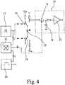
- Fig. 4is a highly simplified circuit diagram of the optoelectronic sensor 1 is shown, which also serves to explain the method according to the invention.
- the optoelectronic sensor 1 according to the inventionnot only is the presence or absence of an object 2 detected in a monitoring area, but also a determination is made the distance of the object 2 from the optoelectronic sensor 1, to which the optoelectronic sensor 1 operates according to the Lichtlaufzeittex.
- VCSEL diode 15serving as the transmitting and receiving component.
- a bridge switch 16is provided, with the aid of which the transmitting in the forward direction operated in the forward direction VCSEL diode 15 is reversed.
- a high-frequency generator 17serves both to generate the electrical transmission pulse and to control the bridge switch 16.
- a bridge switch 16for example, four interconnected monoflops can be used in bridge circuit.
- the very short propagation time of light due to the very high propagation speed of the lightis temporally stretched by stroboscopic scanning.
- a scanneris provided in the evaluation circuit 10 of the optoelectronic sensor 1, which has a storage capacitor 18 and a fast switch 19.
- the electrical received signalis sampled in each case for a very short period of time and the sampling time is continuously shifted between successive periods of the electrical transmission pulse.
- the processing of the very short light transit time pulsesis so much time-stretched that they can be easily evaluated with a microprocessor and parasitic maturities of the evaluation circuit 10, d. H. the electronics have no meaning.
- a low-frequency generator 20 and a mixer 21are provided, wherein the sampling frequency f A of the sampling pulse of the sum of the frequency f 1 of the high-frequency generator 17 and the frequency f 2 of the low-frequency generator 20 results.
- the switch 19can be controlled by a sampling bridge consisting of four monoflops, which has the advantage that thereby the pulse width of the sampling pulse can be shortened to the order of magnitude of the pulse width of the transmission pulse.
- FIG. 4Also shown schematically analog flow control can be a digital flow control realized in which then the sampling pulse is generated from a superposition of the high-frequency transmission frequency f 1 with a second high-frequency frequency f 3 .
- the two frequencies f 1 and f 3have only a very small frequency difference, with the time expansion factor then resulting from the ratio of the high-frequency transmission frequency f 1 to the difference frequency (f 1 -f 3 ).
- two quartz-stable high-frequency oscillatorscan be used, in which the frequency difference is generated by means of a PLL frequency analysis in which every nth pulse is swallowed.
- the evaluation circuit 10still has an amplifier 22 and preferably a microcontroller, so that then a basically known teach-in method can be performed with the optoelectronic sensor 1, in which, for example, reflections from a background or a transparent object, stored and at the subsequent measurement can be considered.
Landscapes
- Physics & Mathematics (AREA)
- Life Sciences & Earth Sciences (AREA)
- General Life Sciences & Earth Sciences (AREA)
- General Physics & Mathematics (AREA)
- Geophysics (AREA)
- Optical Radar Systems And Details Thereof (AREA)
- Photometry And Measurement Of Optical Pulse Characteristics (AREA)
- Geophysics And Detection Of Objects (AREA)
Description
Translated fromGermanDie Erfindung betrifft einen optoelektronischen Sensor, insbesondere eine Reflexlichtschranke oder einen Reflexlichttaster, zum Detektieren eines Objekts in einem Überwachungsbereich, mit einem Gehäuse, mit einer Sende- und Empfangsoptik, mit mindestens einem optoelektronischen Bauelement und mit einer Auswerteschaltung. Daneben betrifft die Erfindung noch ein Verfahren zur Detektion eines Objekts in einem Überwachungsbereich, mit einem optoelektronischen Sensor, wobei ein elektrisches Sendesignal in ein optische Sendesignal umgewandelt wird, das optische Sendesignal in den Überwachungsbereich ausgesendet, von einem Reflektor oder einem Objekt als optisches Empfangssignal zumindest teilweise zum optoelektronischen Sensor zurück reflektiert und in ein elektrische Empfangssignal umgewandelt wirdThe invention relates to an optoelectronic sensor, in particular a reflex light barrier or a diffuse reflection sensor, for detecting an object in a surveillance area, with a housing, with a transmitting and receiving optics, with at least one optoelectronic component and with an evaluation circuit. In addition, the invention also relates to a method for detecting an object in a surveillance area, with an optoelectronic sensor, wherein an electrical transmission signal is converted into an optical transmission signal, the optical transmission signal emitted in the surveillance area, from a reflector or an object as an optical reception signal at least partially reflected back to the optoelectronic sensor and converted into an electrical received signal
Bekannte optoelektronische Sensoren weisen stets einen Lichtsender und mindestens einen Lichtempfänger, d. h. mindestens zwei verschieden optoelektronische Bauelemente auf. Dabei werden als Sendebauelemente, also als lichtemittierende Bauelemente, typischerweise Dioden, vorzugsweise Laserdioden, und als Empfangsbauelemente im allgemeinen Fotodioden verwendet. Optoelektronischen Sensoren können im wesentlichen in drei unterschiedliche Arten unterteilt werden, nämlich in Einwegsysteme, Reflexionssysteme und Tastersysteme.Known optoelectronic sensors always have a light transmitter and at least one light receiver, d. H. at least two different optoelectronic components. Here are used as transmission components, ie as light-emitting components, typically diodes, preferably laser diodes, and as receiving devices in general photodiodes. Optoelectronic sensors can be divided essentially into three different types, namely disposable systems, reflection systems and stylus systems.
Einwegsysteme bestehen einerseits aus einer Sendervorrichtung und andererseits aus einer räumlich von dieser getrennten Empfängervorrichtung. Die Sendervorrichtung und die Empfängervorrichtung werden einander gegenüberliegend an den seitlichen Begrenzungen eines zu überwachenden Bereichs derart angeordnet, so daß von der Sendervorrichtung emittiertes Licht von der Empfängervorrichtung empfangen werden kann. Nachteilig hierbei ist, daß zwei elektronische Geräte benötigt, montiert und mit elektrischer Energie versorgt werden müssen. Im Gegensatz dazu sind bei Reflexionssystemen, die auch als Reflexlichtschranken bezeichnet werden, Sender und Empfänger in einer einzigen Baueinheit, also in einem einzigen Gerät integriert.One-way systems consist on the one hand of a transmitter device and on the other hand of a spatially separated from this receiver device. The transmitter device and the receiver device are disposed opposite to each other at the lateral boundaries of a region to be monitored, so that light emitted from the transmitter device can be received by the receiver device. The disadvantage here is that two electronic devices needed to be mounted and supplied with electrical energy. In contrast, in reflection systems, which are also referred to as reflex light barriers, transmitter and receiver are integrated in a single unit, ie in a single device.
Eine solche eine Sender-/Empfängervorrichtung darstellende Baueinheit wird an einer äußeren Begrenzung des zu überwachenden Bereichs angeordnet, während an der anderen, dieser gegenüberliegenden Begrenzung des zu überwachenden Bereichs ein Reflektor, z. B. ein Tripelspiegel, vorgesehen wird, der von der Sender-/Empfängervorrichtung emittiertes Licht derart auf diese zurück reflektiert, daß es von dem in der Sender-/Empfängervorrichtung integrierten Empfänger empfangen werden kann. Gegenüber dem Einwegsystem bietet die Reflexlichtschranke den Vorteil, daß nur ein elektrischer Anschluß erforderlich ist und der Reflektor aufgrund seiner speziellen Eigenschaft nur relativ grob zur Reflexlichtschranke ausgerichtet werden muß.Such a transmitter / receiver device performing assembly is arranged at an outer boundary of the area to be monitored, while at the other, this opposite boundary of the area to be monitored, a reflector, for. B. a triple mirror is provided, the light emitted by the transceiver device reflects back to it in such a way that it can be received by the receiver integrated in the transceiver device. Compared to the disposable system, the reflex light barrier has the advantage that only one electrical connection is required and the reflector due to its special property only has to be aligned relatively coarse to the reflected light barrier.
Reflexlichtschranken lassen sich aufgrund ihres optischen Aufbaus in zwei Gruppen einteilen. Bei den sogenannten echten Autokollimationssystemen wird die Trennung von Sende- und Empfangsstrahl mit einem halbdurchlässigem Spiegel oder einem Polarisationsfilter durchgeführt. Bei der zweiten Gruppe der Reflexlichtschranken erfolgt eine geometrische Teilung von Sende- und Empfangsstrahl durch eine Sendeoptik und eine versetzt dazu angeordnete separate Empfangsoptik. Lichtsender und Lichtempfänger sind in einem Gehäuse nahezu parallel, jedoch mit geringem Abstand voneinander angeordnet. Eine derartige Reflexlichtschranke mit einer Sendeoptik und einer zweiten Empfangsoptik ist beispielsweise aus der
Den beiden zuvor beschriebenen Systemen - Einwegsystem und Reflexionssystem - ist gemeinsam, daß der Empfänger kein Lichtsignal oder nur ein verringertes Lichtsignal empfängt, wenn sich ein Objekt in dem zu überwachenden Bereich befindet, da dieses Objekt den Strahlengang des von dem Sender emittierten Lichtes vollständig oder zumindest teilweise unterbricht. Der Lichtempfänger detektiert somit im Normalfall - keine Unterbrechung der Überwachungsstrecke - den vom Lichtempfänger ausgesandten Lichtstrahl bzw. die ausgesandten Lichtimpulse.The two systems described above - disposable system and reflection system - have in common that the receiver receives no light signal or only a reduced light signal when an object is in the area to be monitored, since this object the beam path of the emitted light from the transmitter completely or at least partially interrupts. The light receiver thus detects in the normal case - no interruption of the monitoring path - the light emitted by the light receiver or the emitted light pulses.
Grundsätzlich verschieden von dieser Funktionsweise ist die Funktionsweise von optoelektronischen Tastersystemen, auch Reflexlichttaster genannt. Bei diesen Systemen befinden sich der Sender und der Empfänger ebenfalls zusammen in einer Baueinheit, im Unterschied zu eine Reflexlichtschranke ist jedoch kein Reflektor als Bestandteil des Systems vorgesehen. Stattdessen wird das vom Sender in der Sender-/Empfängervorrichtung emittierte Licht an einem zu erkennenden Objekt reflektiert. Fällt wenigstens ein Teil des an dem zu erkennenden Objekt reflektierten Lichtes auf die Sender-/Empfängervorrichtung zurück, so kann dieser reflektierte Lichtanteil von dem Empfänger detektiert werden. Reflexlichttaster sind beispielsweise aus der
Aufgrund der in der Regel schlechter reflektierenden Oberfläche des Objekts im Vergleich zu einem Reflektor, weisen Reflexlichttaster eine geringe Reichweite als Reflexionslichtschranken auf. Reflexlichttaster haben jedoch den Vorteil, daß sie kein zweites aktives Element wie Einweglichtschranken und keinen Reflektor wie Reflexlichtschranken benötigen. Reflexlichttaster zur berührungslosen optoelektronischen Erfassung von Gegenständen arbeiten entweder als energetische V-Lichttaster oder als Lichttaster nach dem Triangulationsprinzip.Due to the generally poor reflective surface of the object compared to a reflector, diffuse reflection sensors have a short range as reflected light barriers. However, reflected light scanners have the advantage that they do not require a second active element such as through-beam sensors and no reflector such as retro-reflective sensors. Diffuse reflection sensors for non-contact optoelectronic detection of objects operate either as energetic V-light sensors or as light sensors according to the triangulation principle.
Beim energetischen V-Lichttaster wird das ausgesendete Licht an dem zu erfassenden Objekt diffus reflektiert. Ein Teil des reflektierten Lichtes trifft auf den Lichtempfänger und löst den Schaltvorgang aus. Ausgewertet werden die beiden Zustände - Reflexion oder keine Reflexion -, die gleichbedeutend sind mit der An- bzw. Abwesenheit eines Gegenstandes im Tastbereich. Systembedingt ist die Tastweite des einfachen energetischen V-Lichttasters daher sehr stark vom Reflexionsgrad des zu überwachenden Objektes abhängig. Lichtsender und Lichtempfänger können dabei eine gemeinsame Sende-/Empfangsoptik aufweisen, wobei hinter der Sende-/Empfangsoptik ein Strahlteiler angeordnet ist, der das vom Objekt reflektierte Licht zum Empfänger umlenkt.With the energetic V-light sensor, the emitted light is reflected diffusely on the object to be detected. Part of the reflected light hits the light receiver and triggers the switching process. The two states - reflection or no reflection - are evaluated, which are synonymous with the presence or absence of an object in the touch area. Due to the system, the scanning distance of the simple energetic V-light sensor is therefore highly dependent on the reflectance of the object to be monitored. Light emitter and light receiver can have a common transmission / reception optics, wherein behind the transmission / reception optics, a beam splitter is arranged, which deflects the reflected light from the object to the receiver.
Die Triangulationslichttaster arbeiten nach dem Doppellinsenprinzip, d. h. die Sendeoptik und die Empfangsoptik sind räumlich getrennt und der Sendestrahl und der Empfangsstrahl bilden einen Winkel zueinander. Der Schnittpunkt von Sendestrahl und Empfangsstrahl bestimmt den maximalen Tastabstand dieser Systeme. Wegen des relativ geringen technischen Aufwandes haben Triangulationslichttaster unter Verwendung von zwei Fotodioden - eine für den Nahbereich und eine für den Fernbereich - allgemeine Verbreitung gefunden. Der Schaltabstand wir dabei von der Lateralposition der Trennlinie zwischen den beiden Fotodioden bestimmt.The triangulation light scanners operate on the double lens principle, d. H. the transmitting optics and the receiving optics are spatially separated and the transmitting beam and the receiving beam form an angle to one another. The intersection of transmit beam and receive beam determines the maximum scanning distance of these systems. Because of the relatively low technical effort, triangulation light scanners using two photodiodes - one for the near range and one for the far range - have found general distribution. The switching distance is determined by the lateral position of the dividing line between the two photodiodes.
Die vorliegende Erfindung betrifft nun einen optoelektronischen Sensor gemäß der zweiten oder dritten Art, d. h. eine Reflexlichtschranke oder einen Reflexlichttaster. Dabei soll im Rahmen der Erfindung unter einer Detektion eines Objekts in einem Überwachungsbereich sowohl die reine Feststellung - Objekt vorhanden oder nicht - als auch eine Bestimmung der Position des Objekts, d. h. der Entfernung des Objekts von dem optoelektronischen Sensor verstanden werden. Eine Sende- und Empfangsoptik kann entweder aus zwei separaten Optiken, d.h. einer Sendeoptik und einer separaten Empfangsoptik oder aus einer einzigen Optik, die dann sowohl Sendeoptik als auch Empfangsoptik ist, bestehen.The present invention now relates to an optoelectronic sensor according to the second or third type, ie a reflected light barrier or a reflected light sensor. It is intended in the context of the invention under a detection of a Object in a surveillance area both the pure statement - object or not - as well as a determination of the position of the object, ie the distance of the object to be understood by the optoelectronic sensor. A transmitting and receiving optics can either consist of two separate optics, ie a transmitting optics and a separate receiving optics or a single optic, which is then both transmitting optics and receiving optics.
Aus der
Die
Die beiden Arten der optoelektronischen Sensoren, bei denen die Sendervorrichtung und die Empfängervorrichtung in einem Gehäuse angeordnet sind, weisen, bedingt durch die räumliche Trennung von Sende- und Empfangsstrahl, jeweils verschiedene Nachteile auf. Sowohl die Verwendung eines halbdurchlässigen Spiegels oder Strahlteilers als auch die benachbarte Anordnung einer Sendeoptik und einer Empfangsoptik führen jeweils dazu, daß der von einem Gegenstand oder einem Reflektor reflektierte Anteil des Lichtes, der auf den Empfänger trifft, verringert wird. Grund dafür ist zum einen der relativ hohe Dämpfungswert der herkömmlichen Strahlteiler, wobei nicht nur das Empfangssignal, sondern auch das Sendesignal den Strahlteiler passieren muß, zum anderen die einbaubedingte geringe Größe der Linsen bei einer Sendeoptik und der separaten Empfangsoptik, wodurch ein relativ geringer Anteil des reflektierten Lichtes auf die Empfangsoptik trifft und somit zum Empfänger geführt wird. Außerdem stellen die zur Trennung von Sende- und Empfangsstrahl erforderlichen Strahlteiler einen erheblichen Kostenfaktor bei der Herstellung der optoelektronischen Sensoren dar.The two types of optoelectronic sensors in which the transmitter device and the receiver device are arranged in a housing have, due to the spatial separation of transmitting and receiving beam, respectively, different disadvantages. Both the use of a semitransparent mirror or beam splitter as well as the adjacent arrangement of a transmitting optics and a receiving optics in each case lead to that of an object or a reflector reflected portion of the light, which hits the receiver is reduced. The reason for this is on the one hand, the relatively high attenuation of the conventional beam splitter, not only the received signal, but also the transmission signal must pass through the beam splitter, on the other hand, the installation small size of the lenses in a transmitting optics and the separate receiving optics, creating a relatively small proportion of reflected light hits the receiving optics and is thus guided to the receiver. In addition, the necessary for the separation of transmit and receive beam beam splitter are a significant cost factor in the production of optoelectronic sensors.
Der vorliegende Erfindung liegt daher die Aufgabe zugrunde, einen eingangs beschriebenen optoelektronischen Sensor sowie ein eingangs beschriebenes Verfahren zur Detektion eines Objekts in einem Überwachungsbereich anzugeben, mit dem auf möglichst einfache Art und Weise ein Objekt möglichst zuverlässig detektiert werden kann.The present invention is therefore based on the object of specifying an optoelectronic sensor described at the outset as well as an initially described method for detecting an object in a monitoring area, with which an object can be detected as reliably as possible in the simplest possible way.
Diese Aufgabe ist bei dem eingangs beschriebenen optoelektronischen Sensor mit den Merkmalen des Patentanspruchs 1 dadurch gelöst, daß ein und dasselbe optoelektronische Bauelement zeitlich nacheinander als Lichtsender und als Lichtempfänger fungiert, so daß nur ein optoelektronisches Bauelement vorgesehen ist, das sowohl als Sendebauelement als auch als Empfangsbauelement fungiert, so dass keine räumliche Trennung zwischen Lichtsender und Lichtempfänger besteht und somit der optische Signalweg innerhalb des optoelektronischen Sensors für das optische Sendesignal und das optische Empfangssignal identisch ist. Das optoelektronische Bauelement kann somit auch als optoelektronisches Sende- und Empfangsbauelement bezeichnet werden. Erfindungsgemäß ist somit die räumliche Trennung von Lichtsender und Lichtempfänger durch eine zeitliche Trennung ersetzt worden. Hierdurch reduzieren sich zunächst die benötigten Bauteile, da anstelle zweier Bauteile, eines Lichtsenders und eines Lichtempfängers, nur ein optoelektronisches Bauteil benötigt wird. Zusätzlich kann auch auf einen Strahlteiler verzichtet werden, wodurch die zuvor beschriebenen Nachteile bei der Verwendung eines Strahlteilers vermieden werden.This object is achieved in the optoelectronic sensor described in the introduction with the features of
Ein weiterer Vorteil, der sich dadurch ergibt, daß nicht mehr ein separater Lichtsender und ein separater Lichtempfänger sondern nur noch ein einziges optoelektronisches Bauteil verwendet wird, besteht darin, daß der Justageaufwand, der ansonsten bei der Ausrichtung von Sender und Empfänger erforderlich ist, entfällt. Durch die Verwendung nur noch eines einzigen optoelektronischen Bauelements weist der optoelektronische Sensor vorzugsweise auch nur noch eine einzige Sende- und Empfangsoptik auf, durch die das optische Sendesignal kollimiert bzw. das optische Empfangssignal auf das optoelektronische Bauelement gelenkt wird.Another advantage that results from the fact that no longer a separate light transmitter and a separate light receiver but only a single is used optoelectronic component, is that the adjustment effort that is otherwise required in the alignment of transmitter and receiver eliminated. By using only a single optoelectronic component, the optoelectronic sensor preferably also has only one single transmitting and receiving optical system, by means of which the optical transmission signal is collimated or the optical received signal is directed to the optoelectronic component.
Bei dem verwendeten optoelektronischen Bauelement kann es sich grundsätzlich um eine herkömmliche Diode handeln. Vorzugsweise wird als optoelektronisches Bauelement jedoch eine Laserdiode, insbesondere eine VCSEL-Diode (Vertical Cavitiy Surface Emitting Laserdiode) verwendet. Der Vorteil einer derartigen VCSEL-Diode besteht zunächst darin, daß sie auch als schnelle Fotodiode verwendet werden kann. Der optische Resonator der VCSEL-Diode sorgt dabei nicht nur für einen gewünschten schmalbandigen Sendeimpuls, sondern fungiert gleichzeitig auch als sehr schmalbandiger Empfangsfilter, dessen Mittenfrequenz automatisch mit der Sendefrequenz gekoppelt ist. Daraus ergibt sich als besonderer Vorteil des erfindungsgemäßen optoelektronischen Sensors, daß er äußerst störfest gegenüber Fremdlicht ist. Die Verwendung eines vergleichbar schmalbandigen Filters vor einem Lichtempfänger ist bei einem herkömmlichen optoelektronischen Sensor aufgrund des Temperaturdriffs der Emissionswellenlänge des Sendebauelements kaum realisierbar.The optoelectronic component used may in principle be a conventional diode. Preferably, however, a laser diode, in particular a VCSEL (Vertical Cavity Surface Emitting Laser Diode), is used as the optoelectronic component. The advantage of such a VCSEL diode is first that it can also be used as a fast photodiode. The optical resonator of the VCSEL diode not only provides a desired narrow-band transmission pulse, but also acts as a very narrow-band receive filter whose center frequency is automatically coupled to the transmission frequency. It follows as a particular advantage of the optoelectronic sensor according to the invention that it is extremely resistant to interference from extraneous light. The use of a comparatively narrow-band filter in front of a light receiver is hardly feasible in a conventional optoelectronic sensor due to the temperature attack of the emission wavelength of the transmission component.
Soll die Diode als Lichtsender fungieren, so wird sie in Durchlaßrichtung betrieben, während sie dann, wenn sie als Lichtempfänger fungieren soll, in Sperrichtung betrieben wird. Bei Beschaltung der Diode mit Vorspannung in Sperrichtung kann diese auch als schnelle Fotodiode eingesetzt werden. Dadurch ergibt sich die Möglichkeit, mit dem erfindungsgemäßen optoelektronischen Sensor nicht nur die Anwesenheit eines Objekts in einem Überwachungsbereich sondern auch dessen Abstand vom optoelektronischen Sensor festzustellen. Der optoelektronische Sensor kann dann auch als Entfernungsmeßgerät eingesetzt werden.If the diode is to act as a light emitter, it is operated in the forward direction, while then, if it is to act as a light receiver, is operated in the reverse direction. When the diode is biased in the reverse direction, it can also be used as a fast photodiode. This results in the possibility of not only detecting the presence of an object in a monitoring area but also its distance from the optoelectronic sensor with the optoelectronic sensor according to the invention. The optoelectronic sensor can then also be used as a distance measuring device.
Entfernungsmeßgeräte basieren dabei auf dem Prinzip, daß bei bekannter Laufzeit eines Signals durch ein Medium und gleichzeitig bekannter Ausbreitungsgeschwindigkeit des Signals in diesem Medium sich die Entfernung als Produkt von Ausbreitungsgeschwindigkeit und Laufzeit ergibt. Aufgrund der extrem hohen Ausbreitungsgeschwindigkeit von Lichtwellen ist dabei auch eine hohe Auswertegeschwindigkeit der verwendeten optoelektronischen Sensoren erforderlich, was durch die Verwendung einer VCSEL-Diode im Sperrbetrieb als Lichtempfänger gegeben ist.Distance measuring devices are based on the principle that at a known transit time of a signal through a medium and at the same time known propagation speed of the signal in this medium, the distance results as the product of propagation velocity and transit time. Due to the extremely high propagation speed of light waves, a high evaluation speed of the optoelectronic sensors used is required, which is given by the use of a VCSEL diode in the blocking mode as a light receiver.
Gemäß einer weiteren vorteilhaften Ausgestaltung der Erfindung, der besondere Bedeutung zukommt, wird der bei der Entfernungsmessung auftretende sehr kurze Licht-Laufzeitimpuls durch stroboskopische Abtastung zeitlich gedehnt. Bei einem Abstand eines Objekts vom optoelektronischen Sensor von einem Meter, woraus sich eine für den Lichtstrahl zurückzulegende Strecke von zwei Metern ergibt, beträgt die Laufzeit des Lichtes lediglich 6,67 ns. Durch die stroboskopische Abtastung wird dieser Impuls soweit gedehnt, daß er von einer Auswerteschaltung mit einem Mikroprozessor problemlos verarbeitet werden kann. Gemäß einer bevorzugten Ausgestaltung weist hierzu der optoelektronische Sensor einen Abtaster mit einem Speicherkondensator und einem schnellen Schalter auf. Der Schalter wird dabei von einem im Vergleich zum Sendepuls gedehnten Abtastimpuls gesteuert.According to a further advantageous embodiment of the invention, which is of particular importance, the very short light transit time pulse occurring during the distance measurement is temporally stretched by stroboscopic scanning. At a distance of an object from the optoelectronic sensor of one meter, resulting in a distance of two meters to be traveled for the light beam, the duration of the light is only 6.67 ns. By stroboscopic scanning of this pulse is stretched so far that it can be easily processed by an evaluation circuit with a microprocessor. According to a preferred embodiment, for this purpose the optoelectronic sensor has a scanner with a storage capacitor and a fast switch. The switch is controlled by a stretched pulse compared to the transmit pulse.
Zur Erzeugung des Abtastimpulses sind bei einer ersten Ausgestaltung des optoelektronischen Sensors ein Hochfrequenzgenerator, ein Niederfrequenzgenerator und ein Mischer vorgesehen, wobei der Sendeimpuls von dem Hochfrequenzgenerator und der Abtastimpuls von dem am Mischer erzeugten Mischprodukt aus der Frequenz des Hochfrequenzgenerators und der Frequenz des Niederfrequenzgenerators abgeleitet wird. Der Niederfrequenzgenerator stellt somit das niederfrequente "Wobbelsignal" zur Verfügung, daß mit dem Signal des Hochfrequenzgenerators gemischt wird.To generate the sampling pulse, a high-frequency generator, a low-frequency generator and a mixer are provided in a first embodiment of the optoelectronic sensor, wherein the transmission pulse from the high-frequency generator and the sampling pulse is derived from the mixed product generated at the mixer from the frequency of the high-frequency generator and the frequency of the low-frequency generator. The low frequency generator thus provides the low frequency "wobble signal" that is mixed with the signal of the high frequency generator.
Gemäß einer alternativen Ausgestaltung des optoelektronischen Sensors sind zur Erzeugung des Abtastimpulses neben dem ersten Hochfrequenzgenerator ein zweiter Hochfrequenzgenerator und ein Mischer vorgesehen. Die beiden Hochfrequenzgeneratoren erzeugen dabei zwei Signale, deren Frequenzen sich nur geringfügig voneinander unterscheiden. Als Mischprodukt wird dabei eine Schwebung erzeugt, aus der wiederum der Abtastimpuls abgeleitet wird.According to an alternative embodiment of the optoelectronic sensor, a second high-frequency generator and a mixer are provided in addition to the first high-frequency generator for generating the sampling pulse. The two high frequency generators generate two signals whose frequencies differ only slightly from each other. As a mixing product while a beat is generated, from which in turn the sampling pulse is derived.
Das eingangs beschriebene Verfahren zur Detektion eines Objekts in einem Überwachungsbereich, mit einem optoelektronischen Sensor, zeichnet sich gemäß Patentanspruch 9 dadurch aus, daß die Umwandlung des elektrischen Sendesignals in das optische Sendesignal und die Umwandlung des optischen Empfangssignals in das elektrische Empfangssignal zeitlich nacheinander durch ein und dasselbe optoelektronische Bauelement erfolgt. Auch das erfindungsgemäße Verfahren zeichnet sich somit zunächst dadurch aus, daß anstelle der räumlichen Trennung von Sender und Empfänger bzw. von Sendesignal und Empfangssignal eine zeitliche Trennung vorgenommen wird.The method described above for detecting an object in a surveillance area, with an optoelectronic sensor, is characterized according to
Dabei ist der optische Signalweg innerhalb des optoelektronischen Sensors für das optische Sendesignal und das optische Empfangssignal identisch. Das optische Sendesignal und das optische Empfangssignal durchlaufen somit denselben optischen Signalweg, jeweils in unterschiedlicher Richtung. Dadurch, daß das optische Sendesignal und das optische Empfangssignal denselben Signalweg durchlaufen, entfällt die ansonsten in Stand der Technik erforderliche Justierung der Sendeoptik und der räumlich daneben angeordneten Empfangsoptik bzw. die Einstellung eines Strahlteilers.In this case, the optical signal path within the optoelectronic sensor for the optical transmission signal and the optical reception signal is identical. The optical transmission signal and the optical reception signal thus pass through the same optical signal path, each in a different direction. The fact that the optical transmission signal and the optical reception signal pass through the same signal path eliminates the adjustment of the transmission optics which is otherwise required in the prior art and the reception optics arranged spatially next to it or the adjustment of a beam splitter.
Auch das erfindungsgemäße Verfahren wird vorteilhafterweise zur Distanzbestimmung eines Objekts in dem Überwachungsbereich benutzt, so daß ein pulsförmiges Sendesignal verwendet wird und die Laufzeit des optischen Signals gemessen und daraus die Entfernung des Objekts bestimmt wird. Wie zuvor im Zusammenhang mit dem erfindungsgemäßen optoelektronischen Sensor bereits beschrieben wird auch bei dem erfindungsgemäßen Verfahren vorteilhafterweise das elektrische Empfangssignal stroboskopisch abgetastet und dadurch zeitlich gedehnt. Dabei wird das elektrische Empfangssignal für einen kurzen Zeitraum abgetastet, wobei der Abtastzeitpunkt kontinuierlich zwischen aufeinanderfolgenden Perioden des Sendeimpulses verschoben wird. Die Ablaufsteuerung für Erzeugung des Abtastimpulses kann dabei im wesentlichen analog oder im wesentlichen digital arbeiten.The method according to the invention is also advantageously used to determine the distance of an object in the monitoring area, so that a pulse-shaped transmission signal is used and the transit time of the optical signal is measured and from this the distance of the object is determined. As already described above in connection with the optoelectronic sensor according to the invention, the electrical received signal is also stroboscopically sampled and thereby stretched in time in the method according to the invention. In this case, the received electrical signal is sampled for a short period of time, wherein the sampling time is continuously shifted between successive periods of the transmission pulse. The sequence control for generating the sampling pulse can operate essentially analog or substantially digital.
Im einzelnen gibt es nun eine Vielzahl von Möglichkeiten, den erfindungsgemäßen optoelektronischen Sensor bzw. das erfindungsgemäße Verfahren zur Detektion eines Objekts auszugestalten und weiterzubilden. Dazu wird verwiesen einerseits auf die den Patentansprüchen 1 und 9 nachgeordneten Patentansprüche, andererseits auf die nachfolgende Beschreibung bevorzugter Ausführungsbeispiele in Verbindung mit der Zeichnung. In der Zeichnung zeigen
- Fig. 1
- eine vereinfachte Darstellung eines optoelektronischen Sensors gemäß dem Stand der Technik,
- Fig. 2
- eine vereinfachte Darstellung eines ersten Ausführungsbeispiels eines erfindungsgemäßen optoelektronischen Sensors,
- Fig. 3
- eine vereinfachte Darstellung eines zweiten Ausführungsbeispiels eines erfindungsgemäßen optoelektronischen Sensors und
- Fig. 4
- ein stark vereinfachtes Schaltbild eines erfindungsgemäßen optoelektronischen Sensors.
- Fig. 1
- a simplified representation of an optoelectronic sensor according to the prior art,
- Fig. 2
- a simplified representation of a first embodiment of an optoelectronic sensor according to the invention,
- Fig. 3
- a simplified representation of a second embodiment of an optoelectronic sensor according to the invention and
- Fig. 4
- a highly simplified circuit diagram of an optoelectronic sensor according to the invention.
Die
Die beiden in den
Die in
Die in den
Als Bauelement 14 eignet sich dabei insbesondere eine VCSEL-Diode 15, die aufgrund ihres optischen Resonators nicht nur einen sehr schmalbandigen Sendestrahl 7 aussendet, sondern aufgrund des beim Empfang als schmalbandiges optisches Filter wirkenden Resonators auch nur einem sehr schmalbandigen Empfangsstrahl 9 detektiert. Dies hat den Vorteil, daß der optoelektronische Sensor 1 sehr störfest ist, wodurch eine Beeinflussung des Meßergebnisses aufgrund von Streulicht verhindert wird. Darüber hinaus kann die VCSEL-Diode 15 auch als sehr schnelle Fotodiode eingesetzt werden.In this case, a
Die in
Bei dem erfindungsgemäßen optoelektronischen Sensor 1 wird von dem als Lichtsender fungierenden Bauelement 14 ein Sendestrahl 7 erzeugt, der durch die Sende- und Empfangsoptik 6 auf den Reflektor 8 (
In
Hierzu werden von der als Sende- und Empfangsbauelement dienenden VCSEL-Diode 15 sehr kurze optische Sendeimpulse mit einer Impulsbreite von nur ca. 1 ns abgestrahlt. Zur Umschaltung der VCSEL-Diode 15 vom Sendebetrieb in den Empfangsbetrieb ist ein Brückenschalter 16 vorgesehen, mit dessen Hilfe die im Sendebetrieb in Durchlaßrichtung betriebene VCSEL-Diode 15 umgepolt wird. Ein Hochfrequenzgenerator 17 dient dabei sowohl zur Erzeugung des elektrischen Sendeimpulses als auch zur Steuerung des Brückenschalters 16. Als Brückenschalter 16 können beispielsweise vier in Brückenschaltung miteinander verschaltete Monoflops dienen.For this purpose, very short optical transmission pulses with a pulse width of only about 1 ns are emitted by the
Der aufgrund der sehr großen Ausbreitungsgeschwindigkeit des Lichtes sehr kurze Licht-Laufzeitimpuls wird durch stroboskopische Abtastung zeitlich gedehnt. Hierzu ist in der Auswerteschaltung 10 des optoelektronischen Sensors 1 ein Abtaster vorgesehen, der einen Speicherkondensator 18 und einen schnellen Schalter 19 aufweist. Dabei wird das elektrische Empfangssignal jeweils für eine sehr kurze Zeitdauer abgetastet und der Abtastzeitpunkt kontinuierlich zwischen aufeinanderfolgenden Perioden des elektrischen Sendeimpulses verschoben. Dadurch wird die Verarbeitung der sehr kurzen Licht-Laufzeitimpulse so stark zeitgedehnt, daß sie problemlos mit einem Mikroprozessor ausgewertet werden können und parasitäre Laufzeiten der Auswerteschaltung 10, d. h. der Elektronik keine Bedeutung mehr haben.The very short propagation time of light due to the very high propagation speed of the light is temporally stretched by stroboscopic scanning. For this purpose, a scanner is provided in the
Zur Erzeugung des Abtastimpulses sind ein Niederfrequenzgenerator 20 und ein Mischer 21 vorgesehen, wobei sich die Abtastfrequenz fA des Abtastimpulses aus der Summe der Frequenz f1 des Hochfrequenzgenerators 17 und der Frequenz f2 des Niederfrequenzgenerators 20 ergibt. Der Schalter 19 kann dabei von einer Abtastbrücke bestehend aus vier Monoflops gesteuert werden, was den Vorteil hat, daß dadurch die Impulsbreite des Abtastimpulses auf die Größenordnung der Impulsbreite des Sendeimpulses verkürzt werden kann. Der Zeitdehnungsfaktor der stroboskopischen Abtastung ergibt sich im vorliegenden Fall als Quotient der Frequenz f1 zur Frequenz f2, so daß bei einem Hochfrequenzsignal von beispielsweise f1 = 1 MHz und einem Niederfrequenzsignal von beispielsweise f2 = 1 kHz ein Zeitdehnungsfaktor von 1000 erreicht wird.To generate the sampling pulse, a low-
Anstelle der anhand von
Die Auswerteschaltung 10 weist noch einen Verstärker 22 und vorzugsweise einen Mikrocontroller auf, so daß dann mit dem optoelektronischen Sensor 1 ein grundsätzlich bekanntes Teach-In-Verfahren durchgeführt werden kann, bei dem beispielsweise Reflektionen von einem Hintergrund oder einem transparenten Objekt eingelernt, gespeichert und bei der nachfolgenden Messung berücksichtigt werden können.The
Claims (17)
- Optoelectronic sensor, especially a reflection photoelectronic barrier or a reflection light sensing device, for detecting an object (2) in a monitored area, with a housing (3), with a transmitting and receiving optics (6), with at least one optoelectronic component, and with an evaluation circuit (10)
characterized in
that a single optoelectronic component (14) acts sequentially in time as a opto-transmitter and as opto-receiver, so that only one optoelectronic component (14) is provided, which functions both as a transmission device as well as a receiving device,
so that there is no spacial separation between the opto-transmitter and the op-to-receiver and therefore the optical signal path within the optoelectronic sensor (1) is identical for the optical transmission signal and the optical received signal. - Optoelectronic sensor according to claim 1,characterized in that only a single transmitting and receiving optics (6) is provided, which comprises at least one lens.
- Optoelectronic sensor according to claim 1 or 2,characterized in that a diode, preferably a laser diode, especially a VCSEL diode (15) (vertical cavity surface emitting laser diode) is provided as optoelectronic component (14), wherein the diode (15) is wired in the forward direction as light emitter and in the reverse direction as light receiver.
- Optoelectronic sensor according to claim 3,characterized in that the diode (15) is switchable from transmission operation into receiving operation via at least one switch, in particular a bridge switch (16), wherein the bridge switch (16) is controlled by a high-frequency generator (17).
- Optoelectronic sensor according to any one of claims 1 to 4,characterized in that the evaluation circuit (10) has a scanner with a storage capacitor (18) and a switch (19).
- Optoelectronic sensor according to claim 5,characterized in that the switch is controlled (19) by a time-stretched scanning pulse.
- Optoelectronic sensor according to claim 6,characterized in that a high frequency generator (17), a low frequency generator (20) and a mixer (21) are provided and that the transmitted pulse is derived from the high frequency generator (18) and the scanning pulse is derived from a mixed product generated by the mixer (21) from the frequency f1 of the high frequency generator (17) and the frequency f2 of the low frequency generator (20).
- Optoelectronic sensor according to claim 6,characterized in that a first high frequency generator, a second high frequency generator and a mixer are provided.
- Process for detecting of an object in a monitored area, with an optoelectronic sensor, especially according to any one of claims 1 to 8, wherein an electrical transmission signal is converted into an optical transmission signal, the optical transmission signal beeing emitted into the monitored area, at least partially reflected back to the optoelectronic sensor by a reflector or an object as an optical received signal and converted into an electrical received signal,
characterized in
that the conversion of the electrical transmission signal into the optical transmission signal and the conversion of the received optical signal into the electrical received signal takes place succession in time by a single optoelectronic component,
so that the optical signal path within the optoelectronic sensor is identical for the optical transmission signal and the optical received signal, i.e. the optical transmission signal and the optical received signal traverse the same optical signal path in different directions. - Process according to claim 9, wherein the electrical transmission signal is pulsed,characterized in that the transit time of the optical signal is measured and the distance of the object is determined from it.
- Process according to claim 10,characterized in that the electrical received signal is stroboscopically scanned so as to be stretched in time.
- Process according to claim 11,characterized in that the electrical received signal is scanned for a short time period and a scanning instant is shifted continuously between successive periods of the transmitted pulse.
- Process according to claim 12,characterized in that the scanning frequency fA is produced by mixing the high transmitted frequency f1 with a second lower frequency f2, wherein the transmitted frequency f1 is preferably in a range of a few 100 kHz to a few MHz, and the second lower frequency f2 is preferably in a range of a few 100 Hz to a few kHz.
- Process according to claim 12,characterized in that the scanning frequency fA is produced by mixing the high frequency f1 with a second high frequency f3, wherein the transmitted frequency f1 and the second frequency f3 preferably are in a range of a few 100 kHz to a few MHz.
- Process according to any one of claims 11 to 14 having a optoelectronic sensor comprising an evaluation circuit,characterized in that the scanning frequency fA is processed by the evaluation circuit is, in particular, shortened and/or compressed.
- Process according to any one of claims 9 to 15,characterized in that the electrical transmission signal has a pulse width of roughly 1 ns.
- Process according to any one of claims 9 to 17, having an evaluation unit comprising a microcontroller,characterized in that a teach-in process can be carried out via the microcontroller.
Applications Claiming Priority (2)
| Application Number | Priority Date | Filing Date | Title |
|---|---|---|---|
| DE10346813 | 2003-10-06 | ||
| DE10346813ADE10346813B4 (en) | 2003-10-06 | 2003-10-06 | An optoelectronic sensor and method for detecting an object in a surveillance area |
Publications (4)
| Publication Number | Publication Date |
|---|---|
| EP1522879A2 EP1522879A2 (en) | 2005-04-13 |
| EP1522879A3 EP1522879A3 (en) | 2007-01-24 |
| EP1522879B1 EP1522879B1 (en) | 2013-05-15 |
| EP1522879B2true EP1522879B2 (en) | 2017-01-18 |
Family
ID=34306329
Family Applications (1)
| Application Number | Title | Priority Date | Filing Date |
|---|---|---|---|
| EP04023748.9AExpired - LifetimeEP1522879B2 (en) | 2003-10-06 | 2004-10-06 | Opto-electronic sensor and method of detecting an object in a surveillance area |
Country Status (3)
| Country | Link |
|---|---|
| US (1) | US7176443B2 (en) |
| EP (1) | EP1522879B2 (en) |
| DE (1) | DE10346813B4 (en) |
Families Citing this family (13)
| Publication number | Priority date | Publication date | Assignee | Title |
|---|---|---|---|---|
| DE102005016556A1 (en) | 2005-04-11 | 2006-10-12 | Sick Ag | Method for operating an optoelectronic sensor |
| DE102005034124A1 (en)* | 2005-07-21 | 2007-01-25 | Sick Ag | Method for securing a bending press and optoelectronic sensor for carrying out such a method |
| US20070071056A1 (en)* | 2005-09-09 | 2007-03-29 | Ye Chen | Laser ranging with large-format VCSEL array |
| DE102006011249B4 (en)* | 2006-03-10 | 2019-04-04 | Pepperl + Fuchs Gmbh | Method for detecting objects |
| DE202006005978U1 (en)* | 2006-03-10 | 2007-07-19 | Pepperl + Fuchs Gmbh | Optoelectronic sensor for determining presence, condition and/or position of object in monitoring region, has light source, which emits radiation and is vertical cavity surface emitting laser or resonant cavity light emitting device |
| US20070278390A1 (en)* | 2006-06-06 | 2007-12-06 | Hong Kong Applied Science And Technology Research Institute Co. Ltd. | Detectors and actuating devices incorporating same |
| DE102011050119A1 (en)* | 2011-05-05 | 2012-11-08 | Sick Ag | Optoelectronic sensor and method for object detection |
| RU2540154C2 (en)* | 2013-04-05 | 2015-02-10 | Открытое акционерное общество "Швабе - Исследования" | Apparatus for detecting optical and optoelectronic |
| RU2609275C1 (en)* | 2015-10-22 | 2017-02-01 | Общество с ограниченной ответственностью "Викрон" | Scanning laser range-finder |
| RU186487U1 (en)* | 2017-05-29 | 2019-01-22 | Открытое акционерное общество "Научно-производственное объединение "Геофизика-НВ" | Device for round-the-clock observation of the position of the radiation spot at a remote object |
| DE102021108372A1 (en) | 2020-04-30 | 2021-11-04 | Ifm Electronic Gmbh | Distance measurement system with a VCSEL array |
| DE102022109546A1 (en) | 2022-04-20 | 2023-10-26 | Trumpf Photonic Components Gmbh | Device for generating a light barrier |
| DE102023105713A1 (en) | 2023-03-08 | 2024-09-12 | Balluff Gmbh | Optoelectronic sensor |
Citations (6)
| Publication number | Priority date | Publication date | Assignee | Title |
|---|---|---|---|---|
| US5648979A (en)† | 1995-12-29 | 1997-07-15 | Samsung Electronics Co. Ltd. | Assembly of VCSEL light source and VCSEL optical detector |
| DE19810231A1 (en)† | 1997-11-07 | 1999-05-27 | Leuze Electronic Gmbh & Co | Optoelectronic device |
| US5978401A (en)† | 1995-10-25 | 1999-11-02 | Honeywell Inc. | Monolithic vertical cavity surface emitting laser and resonant cavity photodetector transceiver |
| DE10018948A1 (en)† | 1999-04-23 | 2000-11-30 | Leuze Electronic Gmbh & Co | Optoelectronic device for detecting objects, uses transmitter to transmit emitted rays of light, a receiver to receive transmitted rays of light and devices to determine distance to an object |
| DE10021590A1 (en)† | 1999-05-08 | 2000-12-07 | Leuze Electronic Gmbh & Co | Optoelectronic device for detecting objects in monitored zone by generating binary signal from output of synchronous detector |
| DE10022054A1 (en)† | 2000-05-06 | 2001-11-15 | Leuze Electronic Gmbh & Co | Optical distance sensor |
Family Cites Families (12)
| Publication number | Priority date | Publication date | Assignee | Title |
|---|---|---|---|---|
| DE2805423B2 (en)* | 1978-02-09 | 1980-05-08 | 6000 Frankfurt | Light barrier arrangement |
| DE3221405A1 (en)* | 1981-09-04 | 1983-03-24 | Robert Bosch Gmbh, 7000 Stuttgart | FUEL INJECTION PUMP FOR INTERNAL COMBUSTION ENGINES |
| DE3419117C2 (en)* | 1984-05-23 | 1986-09-04 | Rheometron AG, Basel | Optoelectric distance measuring device with a time discriminator for the exact determination of the time sequence of electrical impulses |
| DE3513671C3 (en) | 1985-04-16 | 1995-03-23 | Sick Optik Elektronik Erwin | Light switch |
| DE3633181C2 (en)* | 1986-09-30 | 1998-12-10 | Siemens Ag | Reflex light barrier |
| AR241375A1 (en)* | 1988-01-12 | 1992-06-30 | Hawryluk Jose Carlos | Multifunctional electronic command apparatus. |
| DE4238116C2 (en) | 1992-11-12 | 1994-09-01 | Leuze Electronic Gmbh & Co | Retro-reflective sensor with side-by-side transmission and reception optics |
| DE4311691C2 (en) | 1993-04-08 | 1996-07-04 | Sick Erwin Gmbh | Method for adjusting a light distance sensor and light distance sensor |
| DE19933439C2 (en)* | 1998-07-25 | 2003-04-24 | Leuze Electronic Gmbh & Co | Optoelectronic device |
| DE19839305B4 (en)* | 1998-08-28 | 2009-01-15 | Siemens Ag | Retroreflex |
| DE50106232D1 (en)* | 2001-07-03 | 2005-06-16 | Infineon Technologies Ag | OPTO ELECTRONIC TRANSCEIVER MODULE AND METHOD FOR RECEIVING OPTICAL SIGNALS |
| EP1404130A1 (en)* | 2002-09-24 | 2004-03-31 | Matsushita Electric Industrial Co., Ltd. | Method and apparatus for processing a video signal mixed with an additional image signal |
- 2003
- 2003-10-06DEDE10346813Apatent/DE10346813B4/ennot_activeExpired - Fee Related
- 2004
- 2004-10-05USUS10/958,189patent/US7176443B2/ennot_activeExpired - Fee Related
- 2004-10-06EPEP04023748.9Apatent/EP1522879B2/ennot_activeExpired - Lifetime
Patent Citations (6)
| Publication number | Priority date | Publication date | Assignee | Title |
|---|---|---|---|---|
| US5978401A (en)† | 1995-10-25 | 1999-11-02 | Honeywell Inc. | Monolithic vertical cavity surface emitting laser and resonant cavity photodetector transceiver |
| US5648979A (en)† | 1995-12-29 | 1997-07-15 | Samsung Electronics Co. Ltd. | Assembly of VCSEL light source and VCSEL optical detector |
| DE19810231A1 (en)† | 1997-11-07 | 1999-05-27 | Leuze Electronic Gmbh & Co | Optoelectronic device |
| DE10018948A1 (en)† | 1999-04-23 | 2000-11-30 | Leuze Electronic Gmbh & Co | Optoelectronic device for detecting objects, uses transmitter to transmit emitted rays of light, a receiver to receive transmitted rays of light and devices to determine distance to an object |
| DE10021590A1 (en)† | 1999-05-08 | 2000-12-07 | Leuze Electronic Gmbh & Co | Optoelectronic device for detecting objects in monitored zone by generating binary signal from output of synchronous detector |
| DE10022054A1 (en)† | 2000-05-06 | 2001-11-15 | Leuze Electronic Gmbh & Co | Optical distance sensor |
Non-Patent Citations (1)
| Title |
|---|
| APPLIED PHYSICS LETTERS: "Technique for integration of vertical cavity lasers and resonant photodetectors", vol. 73, 1, 6 July 1998, O. SJOLUND ET AL, pages: 1 - 3† |
Also Published As
| Publication number | Publication date |
|---|---|
| DE10346813A1 (en) | 2005-05-19 |
| EP1522879A2 (en) | 2005-04-13 |
| US20050116149A1 (en) | 2005-06-02 |
| EP1522879A3 (en) | 2007-01-24 |
| EP1522879B1 (en) | 2013-05-15 |
| DE10346813B4 (en) | 2013-08-29 |
| US7176443B2 (en) | 2007-02-13 |
Similar Documents
| Publication | Publication Date | Title |
|---|---|---|
| EP2626722B1 (en) | Optoelectronic sensor and method for recording and determining the distance of an object | |
| DE4340756C5 (en) | Laser range finding device | |
| EP2927711B1 (en) | Laser scanner and method for the reliable detection of objects | |
| EP2002208B1 (en) | Device for optically measuring distance and method for operating said type of device | |
| EP3091272B1 (en) | Light grid | |
| EP3130889B1 (en) | Optical distance measuring device | |
| EP2189814B1 (en) | Optoelectronic sensor and method for measuring distance in accordance with the light-crossing time principle | |
| EP2189805B1 (en) | Optoelectronic sensor and method for measuring distance according to time-of-flight | |
| EP2482094B1 (en) | Distance measuring opto-electronic sensor and object detection method | |
| EP1522879B2 (en) | Opto-electronic sensor and method of detecting an object in a surveillance area | |
| EP3232224B1 (en) | Distance-measuring opto-electronic sensor and method for detecting and determining the distance from objects | |
| EP2315045A1 (en) | Measurement of distances or changes in distances | |
| WO2012126659A1 (en) | Measuring apparatus and measuring device for measuring a target object in a multidimensional manner | |
| DE102012112985B3 (en) | Distance measuring opto-electronic sensor for detecting and determining distance of objects in monitoring region, has evaluation unit to determine correlation peak of correlation sequence and measured value for object distance | |
| DE19732776C1 (en) | Optoelectronic device for detecting object in surveillance zone | |
| EP1789754A1 (en) | Device and method for optically measuring distance | |
| DE102018126522A1 (en) | Runtime-based distance measurement using modulated pulse trains of laser pulses | |
| EP2755048A1 (en) | Distance-measuring opto-electronic sensor and method for determing the distance from objects | |
| WO2016116302A1 (en) | Device and method for detecting objects for a motor vehicle | |
| EP3654056A1 (en) | Sensor and method for detecting objects | |
| EP3671276B1 (en) | Optoelectronic sensor and method for detecting an object | |
| EP4184202B1 (en) | Optoelectronic sensor | |
| DE19925553C2 (en) | Optoelectric device | |
| DE10149423B4 (en) | Method and device for measuring distances in optically opaque media | |
| EP4249950A1 (en) | Detection of an object and distance measurement |
Legal Events
| Date | Code | Title | Description |
|---|---|---|---|
| PUAI | Public reference made under article 153(3) epc to a published international application that has entered the european phase | Free format text:ORIGINAL CODE: 0009012 | |
| AK | Designated contracting states | Kind code of ref document:A2 Designated state(s):AT BE BG CH CY CZ DE DK EE ES FI FR GB GR HU IE IT LI LU MC NL PL PT RO SE SI SK TR | |
| AX | Request for extension of the european patent | Extension state:AL HR LT LV MK | |
| RIN1 | Information on inventor provided before grant (corrected) | Inventor name:BIELEFELDT, HARTMUT, DR. Inventor name:BUCK, MARTIN Inventor name:FENSTERLE, ROLF Inventor name:JAROMIR, PALATA Inventor name:LAUTENSCHLAEGER, HOLGER | |
| PUAL | Search report despatched | Free format text:ORIGINAL CODE: 0009013 | |
| AK | Designated contracting states | Kind code of ref document:A3 Designated state(s):AT BE BG CH CY CZ DE DK EE ES FI FR GB GR HU IE IT LI LU MC NL PL PT RO SE SI SK TR | |
| AX | Request for extension of the european patent | Extension state:AL HR LT LV MK | |
| 17P | Request for examination filed | Effective date:20070709 | |
| AKX | Designation fees paid | Designated state(s):DE FR GB | |
| RAP1 | Party data changed (applicant data changed or rights of an application transferred) | Owner name:IFM ELECTRONIC GMBH | |
| GRAP | Despatch of communication of intention to grant a patent | Free format text:ORIGINAL CODE: EPIDOSNIGR1 | |
| GRAS | Grant fee paid | Free format text:ORIGINAL CODE: EPIDOSNIGR3 | |
| GRAA | (expected) grant | Free format text:ORIGINAL CODE: 0009210 | |
| AK | Designated contracting states | Kind code of ref document:B1 Designated state(s):DE FR GB | |
| REG | Reference to a national code | Ref country code:GB Ref legal event code:FG4D Free format text:NOT ENGLISH | |
| REG | Reference to a national code | Ref country code:DE Ref legal event code:R096 Ref document number:502004014166 Country of ref document:DE Effective date:20130711 | |
| PLBI | Opposition filed | Free format text:ORIGINAL CODE: 0009260 | |
| 26 | Opposition filed | Opponent name:LEUZE ELECTRONIC GMBH + CO. KG Effective date:20131219 | |
| REG | Reference to a national code | Ref country code:DE Ref legal event code:R026 Ref document number:502004014166 Country of ref document:DE Effective date:20131219 | |
| PLAX | Notice of opposition and request to file observation + time limit sent | Free format text:ORIGINAL CODE: EPIDOSNOBS2 | |
| PLBB | Reply of patent proprietor to notice(s) of opposition received | Free format text:ORIGINAL CODE: EPIDOSNOBS3 | |
| PLBP | Opposition withdrawn | Free format text:ORIGINAL CODE: 0009264 | |
| PLAY | Examination report in opposition despatched + time limit | Free format text:ORIGINAL CODE: EPIDOSNORE2 | |
| PLBC | Reply to examination report in opposition received | Free format text:ORIGINAL CODE: EPIDOSNORE3 | |
| REG | Reference to a national code | Ref country code:FR Ref legal event code:PLFP Year of fee payment:12 | |
| PLAY | Examination report in opposition despatched + time limit | Free format text:ORIGINAL CODE: EPIDOSNORE2 | |
| PLBC | Reply to examination report in opposition received | Free format text:ORIGINAL CODE: EPIDOSNORE3 | |
| REG | Reference to a national code | Ref country code:FR Ref legal event code:PLFP Year of fee payment:13 | |
| PUAH | Patent maintained in amended form | Free format text:ORIGINAL CODE: 0009272 | |
| STAA | Information on the status of an ep patent application or granted ep patent | Free format text:STATUS: PATENT MAINTAINED AS AMENDED | |
| 27A | Patent maintained in amended form | Effective date:20170118 | |
| AK | Designated contracting states | Kind code of ref document:B2 Designated state(s):DE FR GB | |
| REG | Reference to a national code | Ref country code:DE Ref legal event code:R102 Ref document number:502004014166 Country of ref document:DE | |
| REG | Reference to a national code | Ref country code:FR Ref legal event code:PLFP Year of fee payment:14 | |
| PGFP | Annual fee paid to national office [announced via postgrant information from national office to epo] | Ref country code:FR Payment date:20171023 Year of fee payment:14 | |
| PGFP | Annual fee paid to national office [announced via postgrant information from national office to epo] | Ref country code:GB Payment date:20171024 Year of fee payment:14 | |
| GBPC | Gb: european patent ceased through non-payment of renewal fee | Effective date:20181006 | |
| PG25 | Lapsed in a contracting state [announced via postgrant information from national office to epo] | Ref country code:FR Free format text:LAPSE BECAUSE OF NON-PAYMENT OF DUE FEES Effective date:20181031 | |
| PG25 | Lapsed in a contracting state [announced via postgrant information from national office to epo] | Ref country code:GB Free format text:LAPSE BECAUSE OF NON-PAYMENT OF DUE FEES Effective date:20181006 | |
| PGFP | Annual fee paid to national office [announced via postgrant information from national office to epo] | Ref country code:DE Payment date:20231018 Year of fee payment:20 | |
| REG | Reference to a national code | Ref country code:DE Ref legal event code:R071 Ref document number:502004014166 Country of ref document:DE |