EP1512045B1 - Components and methods for forming and testing electro-optic displays - Google Patents
Components and methods for forming and testing electro-optic displaysDownload PDFInfo
- Publication number
- EP1512045B1 EP1512045B1EP03757283.1AEP03757283AEP1512045B1EP 1512045 B1EP1512045 B1EP 1512045B1EP 03757283 AEP03757283 AEP 03757283AEP 1512045 B1EP1512045 B1EP 1512045B1
- Authority
- EP
- European Patent Office
- Prior art keywords
- electro
- layer
- electrically
- optic medium
- conductive
- Prior art date
- Legal status (The legal status is an assumption and is not a legal conclusion. Google has not performed a legal analysis and makes no representation as to the accuracy of the status listed.)
- Expired - Lifetime
Links
- 238000000034methodMethods0.000titleclaimsdescription110
- 238000012360testing methodMethods0.000titledescription35
- 239000010410layerSubstances0.000claimsdescription302
- 239000012790adhesive layerSubstances0.000claimsdescription99
- 230000008569processEffects0.000claimsdescription78
- 239000004020conductorSubstances0.000claimsdescription42
- 239000000463materialSubstances0.000claimsdescription41
- 230000003287optical effectEffects0.000claimsdescription39
- 239000007787solidSubstances0.000claimsdescription36
- 238000004519manufacturing processMethods0.000claimsdescription32
- 239000002245particleSubstances0.000claimsdescription26
- 230000005684electric fieldEffects0.000claimsdescription14
- 239000011159matrix materialSubstances0.000claimsdescription11
- 230000000694effectsEffects0.000claimsdescription7
- AMGQUBHHOARCQH-UHFFFAOYSA-Nindium;oxotinChemical compound[In].[Sn]=OAMGQUBHHOARCQH-UHFFFAOYSA-N0.000claimsdescription3
- 229910044991metal oxideInorganic materials0.000claimsdescription3
- 150000004706metal oxidesChemical class0.000claimsdescription3
- 238000003475laminationMethods0.000description68
- 239000000758substrateSubstances0.000description50
- 230000001681protective effectEffects0.000description35
- 239000000853adhesiveSubstances0.000description34
- 230000001070adhesive effectEffects0.000description34
- 239000003566sealing materialSubstances0.000description33
- 230000004888barrier functionEffects0.000description32
- 238000000576coating methodMethods0.000description23
- 239000011241protective layerSubstances0.000description20
- 239000011248coating agentSubstances0.000description19
- 230000008859changeEffects0.000description18
- 239000002775capsuleSubstances0.000description17
- 230000007547defectEffects0.000description17
- 230000015572biosynthetic processEffects0.000description14
- 230000002093peripheral effectEffects0.000description12
- 230000007613environmental effectEffects0.000description11
- 239000003094microcapsuleSubstances0.000description10
- 238000007639printingMethods0.000description9
- 230000002411adverseEffects0.000description8
- 238000010030laminatingMethods0.000description8
- BQCADISMDOOEFD-UHFFFAOYSA-NSilverChemical compound[Ag]BQCADISMDOOEFD-UHFFFAOYSA-N0.000description7
- 239000004973liquid crystal related substanceSubstances0.000description7
- 229920000139polyethylene terephthalatePolymers0.000description7
- 239000005020polyethylene terephthalateSubstances0.000description7
- 229910052709silverInorganic materials0.000description7
- 239000004332silverSubstances0.000description7
- 229920002799BoPETPolymers0.000description6
- 238000005520cutting processMethods0.000description6
- 230000008901benefitEffects0.000description5
- 239000003822epoxy resinSubstances0.000description5
- 239000007788liquidSubstances0.000description5
- 239000002985plastic filmSubstances0.000description5
- 229920000647polyepoxidePolymers0.000description5
- 238000012545processingMethods0.000description5
- 238000007789sealingMethods0.000description5
- 229910052782aluminiumInorganic materials0.000description4
- XAGFODPZIPBFFR-UHFFFAOYSA-NaluminiumChemical compound[Al]XAGFODPZIPBFFR-UHFFFAOYSA-N0.000description4
- 239000011230binding agentSubstances0.000description4
- 239000012530fluidSubstances0.000description4
- 238000010348incorporationMethods0.000description4
- 229920006255plastic filmPolymers0.000description4
- 239000011324beadSubstances0.000description3
- 238000002474experimental methodMethods0.000description3
- 238000007689inspectionMethods0.000description3
- 150000002500ionsChemical class0.000description3
- 230000033001locomotionEffects0.000description3
- 229920001296polysiloxanePolymers0.000description3
- 239000002356single layerSubstances0.000description3
- 230000007704transitionEffects0.000description3
- -1Polyethylene terephthalatePolymers0.000description2
- 239000002390adhesive tapeSubstances0.000description2
- QVGXLLKOCUKJST-UHFFFAOYSA-Natomic oxygenChemical compound[O]QVGXLLKOCUKJST-UHFFFAOYSA-N0.000description2
- 230000005540biological transmissionEffects0.000description2
- 230000009172burstingEffects0.000description2
- 238000004140cleaningMethods0.000description2
- 229920001940conductive polymerPolymers0.000description2
- 230000007423decreaseEffects0.000description2
- 230000002950deficientEffects0.000description2
- 238000009792diffusion processMethods0.000description2
- 230000009977dual effectEffects0.000description2
- 238000005516engineering processMethods0.000description2
- 238000005530etchingMethods0.000description2
- 238000011049fillingMethods0.000description2
- 230000006870functionEffects0.000description2
- 239000007789gasSubstances0.000description2
- 239000011521glassSubstances0.000description2
- 238000003384imaging methodMethods0.000description2
- 238000003780insertionMethods0.000description2
- 230000037431insertionEffects0.000description2
- 238000000608laser ablationMethods0.000description2
- 239000001301oxygenSubstances0.000description2
- 229910052760oxygenInorganic materials0.000description2
- 238000001020plasma etchingMethods0.000description2
- 239000005023polychlorotrifluoroethylene (PCTFE) polymerSubstances0.000description2
- 238000002310reflectometryMethods0.000description2
- 230000000717retained effectEffects0.000description2
- 239000000565sealantSubstances0.000description2
- 210000003934vacuoleAnatomy0.000description2
- 229920004439Aclar®Polymers0.000description1
- OKTJSMMVPCPJKN-UHFFFAOYSA-NCarbonChemical compound[C]OKTJSMMVPCPJKN-UHFFFAOYSA-N0.000description1
- 239000004215Carbon black (E152)Substances0.000description1
- 241000270722CrocodylidaeSpecies0.000description1
- JOYRKODLDBILNP-UHFFFAOYSA-NEthyl urethaneChemical compoundCCOC(N)=OJOYRKODLDBILNP-UHFFFAOYSA-N0.000description1
- 239000004831Hot glueSubstances0.000description1
- 229920000134Metallised filmPolymers0.000description1
- 239000005041Mylar™Substances0.000description1
- 239000004820Pressure-sensitive adhesiveSubstances0.000description1
- 229920000297RayonPolymers0.000description1
- 238000005299abrasionMethods0.000description1
- 230000009471actionEffects0.000description1
- 239000002318adhesion promoterSubstances0.000description1
- 239000002313adhesive filmSubstances0.000description1
- 238000007754air knife coatingMethods0.000description1
- 238000004458analytical methodMethods0.000description1
- DQXBYHZEEUGOBF-UHFFFAOYSA-Nbut-3-enoic acid;etheneChemical compoundC=C.OC(=O)CC=CDQXBYHZEEUGOBF-UHFFFAOYSA-N0.000description1
- 230000001413cellular effectEffects0.000description1
- 239000004568cementSubstances0.000description1
- 238000002144chemical decomposition reactionMethods0.000description1
- 230000001427coherent effectEffects0.000description1
- 239000012612commercial materialSubstances0.000description1
- 239000002131composite materialSubstances0.000description1
- 238000010276constructionMethods0.000description1
- 238000007796conventional methodMethods0.000description1
- 238000005336crackingMethods0.000description1
- 238000007766curtain coatingMethods0.000description1
- 230000000593degrading effectEffects0.000description1
- 230000032798delaminationEffects0.000description1
- 238000013461designMethods0.000description1
- LNNWVNGFPYWNQE-GMIGKAJZSA-NdesomorphineChemical compoundC1C2=CC=C(O)C3=C2[C@]24CCN(C)[C@H]1[C@@H]2CCC[C@@H]4O3LNNWVNGFPYWNQE-GMIGKAJZSA-N0.000description1
- 238000001514detection methodMethods0.000description1
- 238000007607die coating methodMethods0.000description1
- 238000003618dip coatingMethods0.000description1
- 238000001312dry etchingMethods0.000description1
- 238000001035dryingMethods0.000description1
- 238000010894electron beam technologyMethods0.000description1
- 239000005038ethylene vinyl acetateSubstances0.000description1
- 238000001125extrusionMethods0.000description1
- 238000007765extrusion coatingMethods0.000description1
- 239000000835fiberSubstances0.000description1
- 239000012467final productSubstances0.000description1
- 239000005357flat glassSubstances0.000description1
- 238000009408flooringMethods0.000description1
- 229910002804graphiteInorganic materials0.000description1
- 239000010439graphiteSubstances0.000description1
- 238000007756gravure coatingMethods0.000description1
- 231100001261hazardousToxicity0.000description1
- 238000010438heat treatmentMethods0.000description1
- 229930195733hydrocarbonNatural products0.000description1
- 150000002430hydrocarbonsChemical class0.000description1
- 238000005286illuminationMethods0.000description1
- 239000012535impuritySubstances0.000description1
- 238000007641inkjet printingMethods0.000description1
- 238000009830intercalationMethods0.000description1
- 238000009685knife-over-roll coatingMethods0.000description1
- 239000012939laminating adhesiveSubstances0.000description1
- 239000006194liquid suspensionSubstances0.000description1
- 230000007774longtermEffects0.000description1
- 238000004020luminiscence typeMethods0.000description1
- 238000007567mass-production techniqueMethods0.000description1
- 230000007246mechanismEffects0.000description1
- 239000012528membraneSubstances0.000description1
- 230000005499meniscusEffects0.000description1
- 229910052751metalInorganic materials0.000description1
- 239000002184metalSubstances0.000description1
- 238000012986modificationMethods0.000description1
- 230000004048modificationEffects0.000description1
- 230000003472neutralizing effectEffects0.000description1
- 239000000382optic materialSubstances0.000description1
- 230000036961partial effectEffects0.000description1
- 229920003023plasticPolymers0.000description1
- 229920002493poly(chlorotrifluoroethylene)Polymers0.000description1
- 229920001200poly(ethylene-vinyl acetate)Polymers0.000description1
- 229920000728polyesterPolymers0.000description1
- 238000002360preparation methodMethods0.000description1
- 238000003825pressingMethods0.000description1
- 239000000047productSubstances0.000description1
- 230000005855radiationEffects0.000description1
- 239000002964rayonSubstances0.000description1
- 238000012827research and developmentMethods0.000description1
- 230000004044responseEffects0.000description1
- 238000007763reverse roll coatingMethods0.000description1
- 230000002441reversible effectEffects0.000description1
- 238000007753roll-to-roll coating processMethods0.000description1
- 229920006395saturated elastomerPolymers0.000description1
- 238000007650screen-printingMethods0.000description1
- 238000012216screeningMethods0.000description1
- 239000004065semiconductorSubstances0.000description1
- 230000035945sensitivityEffects0.000description1
- 238000010008shearingMethods0.000description1
- 239000004447silicone coatingSubstances0.000description1
- 239000002002slurrySubstances0.000description1
- 125000006850spacer groupChemical group0.000description1
- 238000004528spin coatingMethods0.000description1
- 239000007921spraySubstances0.000description1
- 238000005507sprayingMethods0.000description1
- 229910001220stainless steelInorganic materials0.000description1
- 239000010935stainless steelSubstances0.000description1
- 230000003068static effectEffects0.000description1
- 238000003860storageMethods0.000description1
- 239000013589supplementSubstances0.000description1
- 238000010998test methodMethods0.000description1
- 238000007651thermal printingMethods0.000description1
- 229920002803thermoplastic polyurethanePolymers0.000description1
- 238000012546transferMethods0.000description1
- 230000000007visual effectEffects0.000description1
- 238000005406washingMethods0.000description1
- 239000002023woodSubstances0.000description1
Images


Classifications
- B—PERFORMING OPERATIONS; TRANSPORTING
- B05—SPRAYING OR ATOMISING IN GENERAL; APPLYING FLUENT MATERIALS TO SURFACES, IN GENERAL
- B05D—PROCESSES FOR APPLYING FLUENT MATERIALS TO SURFACES, IN GENERAL
- B05D7/00—Processes, other than flocking, specially adapted for applying liquids or other fluent materials to particular surfaces or for applying particular liquids or other fluent materials
- B05D7/50—Multilayers
- B05D7/52—Two layers
- B05D7/54—No clear coat specified
- B05D7/548—No curing step for the last layer
- B05D7/5483—No curing step for any layer
- G—PHYSICS
- G02—OPTICS
- G02F—OPTICAL DEVICES OR ARRANGEMENTS FOR THE CONTROL OF LIGHT BY MODIFICATION OF THE OPTICAL PROPERTIES OF THE MEDIA OF THE ELEMENTS INVOLVED THEREIN; NON-LINEAR OPTICS; FREQUENCY-CHANGING OF LIGHT; OPTICAL LOGIC ELEMENTS; OPTICAL ANALOGUE/DIGITAL CONVERTERS
- G02F1/00—Devices or arrangements for the control of the intensity, colour, phase, polarisation or direction of light arriving from an independent light source, e.g. switching, gating or modulating; Non-linear optics
- G02F1/01—Devices or arrangements for the control of the intensity, colour, phase, polarisation or direction of light arriving from an independent light source, e.g. switching, gating or modulating; Non-linear optics for the control of the intensity, phase, polarisation or colour
- G02F1/165—Devices or arrangements for the control of the intensity, colour, phase, polarisation or direction of light arriving from an independent light source, e.g. switching, gating or modulating; Non-linear optics for the control of the intensity, phase, polarisation or colour based on translational movement of particles in a fluid under the influence of an applied field
- G02F1/166—Devices or arrangements for the control of the intensity, colour, phase, polarisation or direction of light arriving from an independent light source, e.g. switching, gating or modulating; Non-linear optics for the control of the intensity, phase, polarisation or colour based on translational movement of particles in a fluid under the influence of an applied field characterised by the electro-optical or magneto-optical effect
- G02F1/167—Devices or arrangements for the control of the intensity, colour, phase, polarisation or direction of light arriving from an independent light source, e.g. switching, gating or modulating; Non-linear optics for the control of the intensity, phase, polarisation or colour based on translational movement of particles in a fluid under the influence of an applied field characterised by the electro-optical or magneto-optical effect by electrophoresis
- B—PERFORMING OPERATIONS; TRANSPORTING
- B32—LAYERED PRODUCTS
- B32B—LAYERED PRODUCTS, i.e. PRODUCTS BUILT-UP OF STRATA OF FLAT OR NON-FLAT, e.g. CELLULAR OR HONEYCOMB, FORM
- B32B37/00—Methods or apparatus for laminating, e.g. by curing or by ultrasonic bonding
- B32B37/12—Methods or apparatus for laminating, e.g. by curing or by ultrasonic bonding characterised by using adhesives
- B—PERFORMING OPERATIONS; TRANSPORTING
- B32—LAYERED PRODUCTS
- B32B—LAYERED PRODUCTS, i.e. PRODUCTS BUILT-UP OF STRATA OF FLAT OR NON-FLAT, e.g. CELLULAR OR HONEYCOMB, FORM
- B32B37/00—Methods or apparatus for laminating, e.g. by curing or by ultrasonic bonding
- B32B37/14—Methods or apparatus for laminating, e.g. by curing or by ultrasonic bonding characterised by the properties of the layers
- B32B37/16—Methods or apparatus for laminating, e.g. by curing or by ultrasonic bonding characterised by the properties of the layers with all layers existing as coherent layers before laminating
- B32B37/18—Methods or apparatus for laminating, e.g. by curing or by ultrasonic bonding characterised by the properties of the layers with all layers existing as coherent layers before laminating involving the assembly of discrete sheets or panels only
- G—PHYSICS
- G02—OPTICS
- G02B—OPTICAL ELEMENTS, SYSTEMS OR APPARATUS
- G02B1/00—Optical elements characterised by the material of which they are made; Optical coatings for optical elements
- G02B1/10—Optical coatings produced by application to, or surface treatment of, optical elements
- G02B1/14—Protective coatings, e.g. hard coatings
- G—PHYSICS
- G02—OPTICS
- G02F—OPTICAL DEVICES OR ARRANGEMENTS FOR THE CONTROL OF LIGHT BY MODIFICATION OF THE OPTICAL PROPERTIES OF THE MEDIA OF THE ELEMENTS INVOLVED THEREIN; NON-LINEAR OPTICS; FREQUENCY-CHANGING OF LIGHT; OPTICAL LOGIC ELEMENTS; OPTICAL ANALOGUE/DIGITAL CONVERTERS
- G02F1/00—Devices or arrangements for the control of the intensity, colour, phase, polarisation or direction of light arriving from an independent light source, e.g. switching, gating or modulating; Non-linear optics
- G02F1/01—Devices or arrangements for the control of the intensity, colour, phase, polarisation or direction of light arriving from an independent light source, e.g. switching, gating or modulating; Non-linear optics for the control of the intensity, phase, polarisation or colour
- G02F1/13—Devices or arrangements for the control of the intensity, colour, phase, polarisation or direction of light arriving from an independent light source, e.g. switching, gating or modulating; Non-linear optics for the control of the intensity, phase, polarisation or colour based on liquid crystals, e.g. single liquid crystal display cells
- G02F1/1306—Details
- G02F1/1309—Repairing; Testing
- G—PHYSICS
- G02—OPTICS
- G02F—OPTICAL DEVICES OR ARRANGEMENTS FOR THE CONTROL OF LIGHT BY MODIFICATION OF THE OPTICAL PROPERTIES OF THE MEDIA OF THE ELEMENTS INVOLVED THEREIN; NON-LINEAR OPTICS; FREQUENCY-CHANGING OF LIGHT; OPTICAL LOGIC ELEMENTS; OPTICAL ANALOGUE/DIGITAL CONVERTERS
- G02F1/00—Devices or arrangements for the control of the intensity, colour, phase, polarisation or direction of light arriving from an independent light source, e.g. switching, gating or modulating; Non-linear optics
- G02F1/01—Devices or arrangements for the control of the intensity, colour, phase, polarisation or direction of light arriving from an independent light source, e.g. switching, gating or modulating; Non-linear optics for the control of the intensity, phase, polarisation or colour
- G02F1/13—Devices or arrangements for the control of the intensity, colour, phase, polarisation or direction of light arriving from an independent light source, e.g. switching, gating or modulating; Non-linear optics for the control of the intensity, phase, polarisation or colour based on liquid crystals, e.g. single liquid crystal display cells
- G02F1/133—Constructional arrangements; Operation of liquid crystal cells; Circuit arrangements
- G02F1/1333—Constructional arrangements; Manufacturing methods
- G02F1/1339—Gaskets; Spacers; Sealing of cells
- G—PHYSICS
- G02—OPTICS
- G02F—OPTICAL DEVICES OR ARRANGEMENTS FOR THE CONTROL OF LIGHT BY MODIFICATION OF THE OPTICAL PROPERTIES OF THE MEDIA OF THE ELEMENTS INVOLVED THEREIN; NON-LINEAR OPTICS; FREQUENCY-CHANGING OF LIGHT; OPTICAL LOGIC ELEMENTS; OPTICAL ANALOGUE/DIGITAL CONVERTERS
- G02F1/00—Devices or arrangements for the control of the intensity, colour, phase, polarisation or direction of light arriving from an independent light source, e.g. switching, gating or modulating; Non-linear optics
- G02F1/01—Devices or arrangements for the control of the intensity, colour, phase, polarisation or direction of light arriving from an independent light source, e.g. switching, gating or modulating; Non-linear optics for the control of the intensity, phase, polarisation or colour
- G02F1/165—Devices or arrangements for the control of the intensity, colour, phase, polarisation or direction of light arriving from an independent light source, e.g. switching, gating or modulating; Non-linear optics for the control of the intensity, phase, polarisation or colour based on translational movement of particles in a fluid under the influence of an applied field
- G02F1/1675—Constructional details
- B—PERFORMING OPERATIONS; TRANSPORTING
- B32—LAYERED PRODUCTS
- B32B—LAYERED PRODUCTS, i.e. PRODUCTS BUILT-UP OF STRATA OF FLAT OR NON-FLAT, e.g. CELLULAR OR HONEYCOMB, FORM
- B32B2307/00—Properties of the layers or laminate
- B32B2307/20—Properties of the layers or laminate having particular electrical or magnetic properties, e.g. piezoelectric
- B32B2307/202—Conductive
- B—PERFORMING OPERATIONS; TRANSPORTING
- B32—LAYERED PRODUCTS
- B32B—LAYERED PRODUCTS, i.e. PRODUCTS BUILT-UP OF STRATA OF FLAT OR NON-FLAT, e.g. CELLULAR OR HONEYCOMB, FORM
- B32B2457/00—Electrical equipment
- B32B2457/20—Displays, e.g. liquid crystal displays, plasma displays
- G—PHYSICS
- G02—OPTICS
- G02F—OPTICAL DEVICES OR ARRANGEMENTS FOR THE CONTROL OF LIGHT BY MODIFICATION OF THE OPTICAL PROPERTIES OF THE MEDIA OF THE ELEMENTS INVOLVED THEREIN; NON-LINEAR OPTICS; FREQUENCY-CHANGING OF LIGHT; OPTICAL LOGIC ELEMENTS; OPTICAL ANALOGUE/DIGITAL CONVERTERS
- G02F1/00—Devices or arrangements for the control of the intensity, colour, phase, polarisation or direction of light arriving from an independent light source, e.g. switching, gating or modulating; Non-linear optics
- G02F1/01—Devices or arrangements for the control of the intensity, colour, phase, polarisation or direction of light arriving from an independent light source, e.g. switching, gating or modulating; Non-linear optics for the control of the intensity, phase, polarisation or colour
- G02F1/165—Devices or arrangements for the control of the intensity, colour, phase, polarisation or direction of light arriving from an independent light source, e.g. switching, gating or modulating; Non-linear optics for the control of the intensity, phase, polarisation or colour based on translational movement of particles in a fluid under the influence of an applied field
- G02F1/1675—Constructional details
- G02F1/1679—Gaskets; Spacers; Sealing of cells; Filling or closing of cells
- G02F1/1681—Gaskets; Spacers; Sealing of cells; Filling or closing of cells having two or more microcells partitioned by walls, e.g. of microcup type
- G—PHYSICS
- G02—OPTICS
- G02F—OPTICAL DEVICES OR ARRANGEMENTS FOR THE CONTROL OF LIGHT BY MODIFICATION OF THE OPTICAL PROPERTIES OF THE MEDIA OF THE ELEMENTS INVOLVED THEREIN; NON-LINEAR OPTICS; FREQUENCY-CHANGING OF LIGHT; OPTICAL LOGIC ELEMENTS; OPTICAL ANALOGUE/DIGITAL CONVERTERS
- G02F1/00—Devices or arrangements for the control of the intensity, colour, phase, polarisation or direction of light arriving from an independent light source, e.g. switching, gating or modulating; Non-linear optics
- G02F1/01—Devices or arrangements for the control of the intensity, colour, phase, polarisation or direction of light arriving from an independent light source, e.g. switching, gating or modulating; Non-linear optics for the control of the intensity, phase, polarisation or colour
- G02F1/165—Devices or arrangements for the control of the intensity, colour, phase, polarisation or direction of light arriving from an independent light source, e.g. switching, gating or modulating; Non-linear optics for the control of the intensity, phase, polarisation or colour based on translational movement of particles in a fluid under the influence of an applied field
- G02F1/1675—Constructional details
- G02F2001/1678—Constructional details characterised by the composition or particle type
- G—PHYSICS
- G02—OPTICS
- G02F—OPTICAL DEVICES OR ARRANGEMENTS FOR THE CONTROL OF LIGHT BY MODIFICATION OF THE OPTICAL PROPERTIES OF THE MEDIA OF THE ELEMENTS INVOLVED THEREIN; NON-LINEAR OPTICS; FREQUENCY-CHANGING OF LIGHT; OPTICAL LOGIC ELEMENTS; OPTICAL ANALOGUE/DIGITAL CONVERTERS
- G02F2202/00—Materials and properties
- G02F2202/28—Adhesive materials or arrangements
- G—PHYSICS
- G02—OPTICS
- G02F—OPTICAL DEVICES OR ARRANGEMENTS FOR THE CONTROL OF LIGHT BY MODIFICATION OF THE OPTICAL PROPERTIES OF THE MEDIA OF THE ELEMENTS INVOLVED THEREIN; NON-LINEAR OPTICS; FREQUENCY-CHANGING OF LIGHT; OPTICAL LOGIC ELEMENTS; OPTICAL ANALOGUE/DIGITAL CONVERTERS
- G02F2203/00—Function characteristic
- G02F2203/69—Arrangements or methods for testing or calibrating a device
- Y—GENERAL TAGGING OF NEW TECHNOLOGICAL DEVELOPMENTS; GENERAL TAGGING OF CROSS-SECTIONAL TECHNOLOGIES SPANNING OVER SEVERAL SECTIONS OF THE IPC; TECHNICAL SUBJECTS COVERED BY FORMER USPC CROSS-REFERENCE ART COLLECTIONS [XRACs] AND DIGESTS
- Y10—TECHNICAL SUBJECTS COVERED BY FORMER USPC
- Y10T—TECHNICAL SUBJECTS COVERED BY FORMER US CLASSIFICATION
- Y10T156/00—Adhesive bonding and miscellaneous chemical manufacture
- Y10T156/10—Methods of surface bonding and/or assembly therefor
- Y—GENERAL TAGGING OF NEW TECHNOLOGICAL DEVELOPMENTS; GENERAL TAGGING OF CROSS-SECTIONAL TECHNOLOGIES SPANNING OVER SEVERAL SECTIONS OF THE IPC; TECHNICAL SUBJECTS COVERED BY FORMER USPC CROSS-REFERENCE ART COLLECTIONS [XRACs] AND DIGESTS
- Y10—TECHNICAL SUBJECTS COVERED BY FORMER USPC
- Y10T—TECHNICAL SUBJECTS COVERED BY FORMER US CLASSIFICATION
- Y10T428/00—Stock material or miscellaneous articles
- Y10T428/14—Layer or component removable to expose adhesive
- Y10T428/1476—Release layer
Definitions
- bistableand “bistability” are used herein in their conventional meaning in the art to refer to displays comprising display elements having first and second display states differing in at least one optical property, and such that after any given element has been driven, by means of an addressing pulse of finite duration, to assume either its first or second display state, after the addressing pulse has terminated, that state will persist for at least several times, for example at least four times, the minimum duration of the addressing pulse required to change the state of the display element.
- some particle-based electrophoretic displays capable of gray scaleare stable not only in their extreme black and white states but also in their intermediate gray states, and the same is true of some other types of electro-optic displays. This type of display is properly called “multi-stable” rather than bistable, although for convenience the term “bistable” may be used herein to cover both bistable and multi-stable displays.
- electrophoretic displaysare often opaque (since the particles substantially block transmission of visible light through the display) and operate in a reflective mode
- electrophoretic displayscan be made to operate in a so-called "shutter mode" in which the particles are arranged to move laterally within the display so that the display has one display state which is substantially opaque and one which is light-transmissive.
- shutter modein which the particles are arranged to move laterally within the display so that the display has one display state which is substantially opaque and one which is light-transmissive.
- Dielectrophoretic displayswhich are similar to electrophoretic displays but rely upon variations in electric field strength, can operate in a similar mode; see U.S. Patent No. 4,418,346 .
- Other types of electro-optic displaysmay also be capable of operating in shutter mode.
- electro-optic displaysespecially flexible displays
- sealing the displayto prevent ingress of materials from the environment (and/or, in some cases, egress of components of the electro-optic medium).
- organic light emitting diodeswhich may be useful as the electro-optic medium of a display
- this inventionprovides sealed electro-optic displays.
- the electrically-conductive layermay comprise a metal oxide, for example indium tin oxide.
- the front plane laminatemay have a conductive via in electrical contact with the electrically-conductive layer and extending therefrom through or past the layer of electro-optic medium and the adhesive layer.
- a conductive viain electrical contact with the electrically-conductive layer and extending therefrom through or past the layer of electro-optic medium and the adhesive layer.
- the conductive viamay be formed from a deformable material, such as a material comprising conductive particles dispersed in a polymeric matrix.
- a contact pad of electrically-conductive materialmay be interposed between the electrically-conductive layer and the conductive via.
- the release sheet of the front plane laminatemay be provided with a second electrically-conductive layer.
- this disclosureprovides a third article of manufacture (front plane laminate) comprising, in order: a light-transmissive electrically-conductive layer; a layer of a solid electro-optic medium in electrical contact with the electrically-conductive layer; and an adhesive layer.
- the third front plane laminate of the disclosurefurther comprises a conductive via in electrical contact with the electrically-conductive layer and extending therefrom through or past the layer of electro-optic medium and the adhesive layer.
- the electro-optic display of the present disclosuremay be provided with a protective and/or barrier layer disposed on the opposed side of the electrically-conductive layer from the electro-optic medium.
- a layer of transparent adhesivemay be used to secure the protective and/or barrier layer to the electrically-conductive layer.
- the electro-optic displaymay have a sealing material disposed around at least part of the periphery of the layer of electro-optic medium.
- a protective and/or barrier layeris provided extending beyond the periphery of the electro-optic medium, and a sealing material is placed around at least part of the periphery of the electro-optic medium between the protective and/or barrier layer and the backplane.
- the contacting of the adhesive layer with the backplaneis desirably effected under about 20 to about 60 per cent relative humidity.
- the processmay include applying ionized particles to the front plane laminate during at least one of the removal of the release sheet from the adhesive layer and the contacting of the adhesive layer with the backplane.
- the release sheetmay be provided with a second electrically-conductive layer, and the process include applying between the light-transmissive electrically-conductive layer and the second electrically-conductive layer a voltage sufficient to change the optical state of the electro-optic medium.
- this disclosureprovides a process for forming an electro-optic display. This process comprises:
- connection areamay be formed by an aperture extending through the electro-optic medium and the adhesive layer so that the connection area is surrounded by the electro-optic medium and the adhesive layer.
- the front assemblymay comprise a release sheet disposed adjacent the adhesive layer on the opposed side thereof from the layer of electro-optic medium, and this release sheet be removed from the adhesive layer before the front assembly is laminated to the backplane.
- the step of removing the electro-optic medium and the adhesive layer from a portion of the front assemblymay also include removing the release sheet from a portion of the front assembly, so that the connection area is free from the release sheet.
- the release sheetmay provided with a second electrically-conductive layer, and the process may include applying between the light-transmissive electrically-conductive layer and the second electrically-conductive layer a voltage sufficient to change the optical state of the electro-optic medium.
- the conductive viamay be present in the front assembly prior to the lamination step, or may be formed during the lamination step.
- the material which will form the conductive viamay be placed on the backplane prior to the lamination step, so that formation of the conductive via occurs during the lamination of the front assembly to the backplane.
- the front assemblymay have a front contact pad of electrically-conductive material overlying part of the electrically-conductive layer, and the connection area may be formed so as to expose at least part of the front contact pad.
- a sealing materialmay be placed around at least part of the periphery of the front assembly.
- this protective and/or barrier layermay extend beyond the periphery of the electro-optic medium, and the sealing material be placed around at least part of the periphery of the electro-optic medium between the protective and/or barrier layer and the backplane.
- This process of the present disclosuremay include placing a release sheet over the adhesive layer, the release sheet being removed from the adhesive layer before lamination of the front assembly to the backplane.
- the release sheetmay be provided with a second electrically-conductive layer, and the process may include applying between the light-transmissive electrically-conductive layer and the second electrically-conductive layer a voltage sufficient to change the optical state of the electro-optic medium.
- the processmay include placing a deformable electrically-conductive material on the contact pad of the backplane before laminating the front assembly to the backplane, so that the electrically-conductive layer in the connection area is connected to the contact pad via the deformable electrically-conductive material.
- the second testing method of the disclosurecomprises:
- the present inventionprovides an article of manufacture (hereinafter referred to for convenience as a "front plane laminate” or "FPL”) according to appended independent claim 1.
- FPLfront plane laminate
- the light-transmissive electrically-conductive layer of the front plane laminateserves the dual purpose of forming the front electrode of the display which is eventually formed from the front plane laminate, and of providing mechanical integrity to the front plane laminate, thereby permitting the front plane laminate to be handled in a manner which would or might not be possible with a structure comprising only the electro-optic medium and the adhesive layers.
- the electrically-conductive layermay be a single layer, provided that this single layer has the necessary electrical conductivity and mechanical properties; for example, the electrically-conductive layer could comprise a relatively thick (about 100-175 ⁇ m) layer of a conductive polymer.
- the term "light-transmissive"is used herein to mean that the layer thus designated transmits sufficient light to enable an observer, looking through that layer, to observe the change in display states of the electro-optic medium, which will be normally be viewed through the electrically-conductive layer and adjacent substrate (if present).
- the substratewill be typically be a polymeric film, and will normally have a thickness in the range of about 1 to about 25 mil (25 to 634 ⁇ m), preferably about 2 to about 10 mil (51 to 254 ⁇ m).
- the electrically-conductive layeris conveniently a thin layer of. for example, aluminum or indium-tin-oxide (ITO), or may be a conductive polymer.
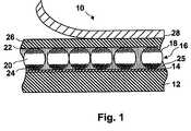
- the white particles 22move to the positive electrode and the black particles 24 move to the negative electrode, so that the layer 16 appears, to an observer viewing the display through the substrate 12, white or black depending upon whether the layer 14 is positive or negative relative to the backplane at any point within the final display.
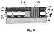
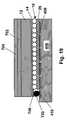
- Figure 9illustrates a front plane laminate (generally designated 210) in which the filling of the aperture 202 has effected before lamination.
- the aperture 202 shown in Figure 8has been filled with a conductive material to form a conductive via 204 extending from the conductive layer 14 to the exposed surface of the release sheet 28.
- the via 204may be formed from any conductive material, though the use of a deformable conductive material, for example a material comprising conductive particles in a polymeric matrix, is convenient. Conductive materials of this type include silver ink, silver-filled epoxy resin, metal-containing silicones and other materials. Alternatively, the via 204 could be formed from a conductive tape.
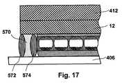
- protective layer 412, front plane laminate 210 and backplane 406are laminated together by advancing stage 416 in the direction of arrow A under roller 414, while the stack of material on stage 416 is held at a specific elevated temperature, desirably in the range of 50-150°C, and preferably in the range of 80-110°C for hot melt adhesives such as ethylene vinyl acetate.
- Roller 414may be heated or un-heated, and applies a pressure desirably in the range of 0.2 to 0.5 MPa and preferably in the range of 0.35 to 0.5 MPa.
- the lamination process shown in Figure 10is a "piece-to-piece" process, in which individual cut pieces of front plane laminate are laminated to individual backplanes.
- the lamination processcould also be effected in a roll-to-roll mode, with a web of front plane laminate being laminated to a web comprising multiple backplanes formed on a flexible substrate; such a web might make use of transistors formed from polymeric semiconductors, as described in certain of the aforementioned E Ink and MIT patents and published applications.
- the lamination processis carried out at about room temperature, e.g., in the range of 15 to 25° C. In addition to relative humidity and temperature, other environmental parameters are desirably controlled.
- the lamination processis desirably carried out in a clean room environment with a low particle count to improve manufacturing yields.
- the fillet seal 520 shown in Figure 11has advantages from a display processing and manufacturing standpoint, as it is easily integrated into the other steps used for manufacturing the display.
- the other edge seal geometries shown in Figures 12 to 17require protective layer 412 (and in some cases, also the substrate 12) to be a different size from the layer of electro-optic medium, and such a size difference may require additional processing and/or manufacturing steps, which may complicate the overall display manufacturing process.
- the adhesive layer of the front plane laminateis subsequently coated in the same pattern as the electro-optic medium, so that in the final web of front plane laminate, part of the tab 926 is free from both electro-optic medium and adhesive layer, so that there is no need to remove these two layers from a portion of the conductive layer before lamination of the front plane laminate to a backplane.
- Figure 22illustrates a process similar to that of Figure 21 but in which the electro-optic medium is applied as a series of patches 930 rather than as a continuous strip, with each patch 930 being used for one display.
- a modification of the process of Figure 22may be used to provide a front plane laminate suitable for use with the true underfill seal of Figure 14 . If the conductive layer is modified to extend over the whole surface of the web 922 of substrate material and the electro-optic medium is coated as appropriately-sized patches 930, severing the web 922 between adjacent patches will provide pieces of front plane laminate in which the substrate and conductive layer extend beyond the periphery of the layer of electro-optic medium all around the electro-optic medium, as required for formation of the true underfill seal of Figure 14 .
Landscapes
- Physics & Mathematics (AREA)
- Nonlinear Science (AREA)
- Optics & Photonics (AREA)
- General Physics & Mathematics (AREA)
- Chemical & Material Sciences (AREA)
- Life Sciences & Earth Sciences (AREA)
- Electrochemistry (AREA)
- Health & Medical Sciences (AREA)
- Chemical Kinetics & Catalysis (AREA)
- Molecular Biology (AREA)
- Crystallography & Structural Chemistry (AREA)
- Engineering & Computer Science (AREA)
- Wood Science & Technology (AREA)
- Mathematical Physics (AREA)
- Electrochromic Elements, Electrophoresis, Or Variable Reflection Or Absorption Elements (AREA)
- Devices For Indicating Variable Information By Combining Individual Elements (AREA)
- Laminated Bodies (AREA)
Description
- The present disclosure relates to processes and components for forming electro-optic displays. More specifically, this disclosure relates to such processes and components for forming electro-optic displays containing an electro-optic medium which is a solid (such displays may hereinafter for convenience be referred to as "solid electro-optic displays"), in the sense that the electro-optic medium has solid external surfaces, although the medium may, and often does, have internal liquid- or gas-filled spaces, and to methods for assembling displays using such an electro-optic medium. Thus, the term "solid electro-optic displays" includes encapsulated electrophoretic displays, encapsulated liquid crystal displays, and other types of displays discussed below.
- The present invention relates to an article and to a process for producing an electrophoretic display as defined in the claims.
- The term "electro-optic", as applied to a material or a displays, is used herein in its conventional meaning in the imaging art to refer to a material having first and second display states differing in at least one optical property, the material being changed from its first to its second display state by application of an electric field to the material. Although the optical property is typically color perceptible to the human eye, it may be another optical property, such as optical transmission, reflectance, luminescence or, in the case of displays intended for machine reading, pseudo-color in the sense of a change in reflectance of electromagnetic wavelengths outside the visible range.
- The terms "bistable." and "bistability" are used herein in their conventional meaning in the art to refer to displays comprising display elements having first and second display states differing in at least one optical property, and such that after any given element has been driven, by means of an addressing pulse of finite duration, to assume either its first or second display state, after the addressing pulse has terminated, that state will persist for at least several times, for example at least four times, the minimum duration of the addressing pulse required to change the state of the display element. It is shown in published
U.S. Patent Application No. 2002/0180687 that some particle-based electrophoretic displays capable of gray scale are stable not only in their extreme black and white states but also in their intermediate gray states, and the same is true of some other types of electro-optic displays. This type of display is properly called "multi-stable" rather than bistable, although for convenience the term "bistable" may be used herein to cover both bistable and multi-stable displays. - Several types of electro-optic displays are known. One type of electro-optic display is a rotating bichromal member type as described, for example, in
U.S. Patents Nos. 5,808,783 ;5,777,782 ;5,760,761 ;6,054,071 6,055,091 ;6,097,531 ;6,128,124 ;6,137,467 ; and6,147,791 (although this type of display is often referred to as a "rotating bichromal ball" display, the term "rotating bichromal member" is preferred as more accurate since in some of the patents mentioned above the rotating members are not spherical). Such a display uses a large number of small bodies (typically spherical or cylindrical) which have two or more sections with differing optical characteristics, and an internal dipole. These bodies are suspended within liquid-filled vacuoles within a matrix, the vacuoles being filled with liquid so that the bodies are free to rotate. The appearance of the display is changed to applying an electric field thereto, thus rotating the bodies to various positions and varying which of the sections of the bodies is seen through a viewing surface. This type of electro-optic medium is typically bistable. - Another type of electro-optic display uses an electrochromic medium, for example an electrochromic medium in the form of a nanochromic film comprising an electrode formed at least in part from a semi-conducting metal oxide and a plurality of dye molecules capable of reversible color change attached to the electrode; see, for exampleO'Regan, B., et al., Nature 1991, 353, 737; andWood, D., Information Display, 18(3), 24 (March 2002). See alsoBach, U., et al., Adv. Mater., 2002, 14(11), 845. Nanochromic films of this type are also described, for example, in
U.S. Patent No. 6,301,038 , International Application Publication No.WO 01/27690 10/249,128, filed March 18, 2003 - Another type of electro-optic display, which has been the subject of intense research and development for a number of years, is the particle-based electrophoretic display, in which a plurality of charged particles move through a suspending fluid under the influence of an electric field. Electrophoretic displays can have attributes of good brightness and contrast, wide viewing angles, state bistability, and low power consumption when compared with liquid crystal displays. Nevertheless, problems with the long-term image quality of these displays have prevented their widespread usage. For example, particles that make up electrophoretic displays tend to settle, resulting in inadequate service-life for these displays.
- Numerous patents and applications assigned to or in the names of the Massachusetts Institute of Technology (MIT) and E Ink Corporation have recently been published describing encapsulated electrophoretic media. Such encapsulated media comprise numerous small capsules, each of which itself comprises an internal phase containing electrophoretically-mobile particles suspended in a liquid suspension medium, and a capsule wall surrounding the internal phase. Typically, the capsules are themselves held within a polymeric binder to form a coherent layer positioned between two electrodes. Encapsulated media of this type are described, for example, in
U.S. Patents Nos. 5,930,026 ;5,961,804 ;6,017,584 ;6,067,185 ;6,118,426 ;6,120,588 ;6,120,839 ;6,124,851 ;6,130,773 ;6,130,774 ;6,172,798 ;6,177,921 ;6,232,950 ;6,249,721 ;6,252,564 ;6,262,706 ;6,262,833 ;6,300,932 ;6,312,304 ;6,312,971 ;6,323,989 ;6,327,072 ;6,376,828 ;6,377,387 ;6,392,785 ;6,392,786 ;6,413,790 ;6,422,687 ;6,445,374 ;6,445,489 ;6,459,418 ;6,473,072 ;6,480,182 ;6,498,114 ;6,504,524 ;6,506,438 ;6,512,354 ;6,515,649 ;6,518,949 ;6,521,489 ;6,531,997 ;6,535,197 ;6,538,801 ; and6,545,291 ; andU.S. Patent Applications Publication Nos. 2002/0019081 ;2002/0021270 ;2002/0053900 ;2002/0060321 ;2002/0063661 ;2002/0063677 ;2002/0090980 ;2002/0106847 ;2002/0113770 ;2002/0130832 ;2002/0131147 ;2002/0145792 ;2002/0154382 ,2002/0171910 ;2002/0180687 ;2002/0180688 ;2002/0185378 ;2003/0011560 ;2003/0011867 ;2003/0011868 ;2003/0020844 ;2003/0025855 ;2003/0034949 ;2003/0038755 ; and2003/0053189 ; and International Applications Publication Nos.WO 99/67678 WO 00/05704 WO 00/20922 WO 00/26761 WO 00/38000 WO 00/38001 WO 00/36560 WO 00/67110 WO 00/67327 WO 01/07961 WO 01/08241 - Many of the aforementioned patents and applications recognize that the walls surrounding the discrete microcapsules in an encapsulated electrophoretic medium could be replaced by a continuous phase, thus producing a so-called polymer-dispersed electrophoretic display in which the electrophoretic medium comprises a plurality of discrete droplets of an electrophoretic fluid and a continuous phase of a polymeric material, and that the discrete droplets of electrophoretic fluid within such a polymer-dispersed electrophoretic display may be regarded as capsules or microcapsules even though no discrete capsule membrane is associated with each individual droplet; see for example, the aforementioned
2002/0131147 - An encapsulated electrophoretic display typically does not suffer from the clustering and settling failure mode of traditional electrophoretic devices and provides further advantages, such as the ability to print or coat the display on a wide variety of flexible and rigid substrates. (Use of the word "printing" is intended to include all forms of printing and coating, including, but without limitation: pre-metered coatings such as patch die coating, slot or extrusion coating, slide or cascade coating, curtain coating; roll coating such as knife over roll coating, forward and reverse roll coating; gravure coating; dip coating; spray coating; meniscus coating; spin coating; brush coating; air knife coating; silk screen printing processes; electrostatic printing processes; thermal printing processes; ink jet printing processes; and other similar techniques.) Thus, the resulting display can be flexible. Further, because the display medium can be printed (using a variety of methods), the display itself can be made inexpensively.
- A related type of electrophoretic display is a so-called "microcell electrophoretic display". In a microcell electrophoretic display, the charged particles and the suspending fluid are not encapsulated within microcapsules but instead are retained within a plurality of cavities formed within a carrier medium, typically a polymeric film. See, for example, International Application Publication No.
WO 02/01281 US Application No. 2002-0075556 , both assigned to Sipix Imaging, Inc. - Although electrophoretic displays are often opaque (since the particles substantially block transmission of visible light through the display) and operate in a reflective mode, electrophoretic displays can be made to operate in a so-called "shutter mode" in which the particles are arranged to move laterally within the display so that the display has one display state which is substantially opaque and one which is light-transmissive. See, for example, the aforementioned
U.S. Patents Nos. 6,130,774 and6,172,798 , andU.S. Patents Nos. 5,872,552 ;6,144,361 ;6,271,823 ;6,225,971 ; and6,184,856 . Dielectrophoretic displays, which are similar to electrophoretic displays but rely upon variations in electric field strength, can operate in a similar mode; seeU.S. Patent No. 4,418,346 . Other types of electro-optic displays may also be capable of operating in shutter mode. - Many of the components used in solid electro-optic displays, and the methods used to manufacture such displays, are derived from technology used in liquid crystal displays (LCD's), which are of course also electro-optic displays, though using a liquid rather than a solid medium. For example, solid electro-optic displays may make use of an active matrix backplane comprising an array of transistors or diodes and a corresponding array of pixel electrodes, and a "continuous" front electrode (in the sense of an electrode which extends over multiple pixels and typically the whole display) on a transparent substrate, these components being essentially the same as in LCD's. However, the methods used for assembling LCD's cannot be used with solid electro-optic displays. LCD's are normally assembled by forming the backplane and front electrode on separate glass substrates, then adhesively securing these components together leaving a small aperture between them, placing the resultant assembly under vacuum, and immersing the assembly in a bath of the liquid crystal, so that the liquid crystal flows through the aperture between the backplane and the front electrode. Finally, with the liquid crystal in place, the aperture is sealed to provide the final display.
- This LCD assembly process cannot readily be transferred to solid electro-optic displays. Because the electro-optic material is solid, it must be present between the backplane and the front electrode before these two integers are secured to each other. Furthermore, in contrast to a liquid crystal material, which is simply placed between the front electrode and the backplane without being attached to either, a solid electro-optic medium normally needs to be secured to both; in most cases the solid electro-optic medium is formed on the front electrode, since this is generally easier than forming the medium on the circuitry-containing backplane, and the front electrode/electro-optic medium combination is then laminated to the backplane, typically by covering the entire surface of the electro-optic medium with an adhesive and laminating under heat, pressure and possibly vacuum.
- As discussed in the aforementioned
U.S. Patent No. 6,312,304 , the manufacture of solid electro-optic displays also presents problems in that the optical components (the electro-optic medium) and the electronic components (in the backplane) have differing performance criteria. For example, it is desirable for the optical components to optimize reflectivity, contrast ratio and response time, while it is desirable for the electronic components to optimize conductivity, voltage-current relationship, and capacitance, or to possess memory, logic, or other higher-order electronic device capabilities. Therefore, a process for manufacturing an optical component may not be ideal for manufacturing an electronic component, and vice versa. For example, a process for manufacturing an electronic component can involve processing under high temperatures. The processing temperature can be in the range from about 300°C. to about 600°C. Subjecting many optical components to such high temperatures, however, can be harmful to the optical components by degrading the electro-optic medium chemically or by causing mechanical damage. - This patent describes a method of manufacturing an electro-optical display comprising providing a modulating layer including a first substrate and an electro-optical material provided adjacent the first substrate, the modulating layer being capable of changing a visual state upon application of an electric field; providing a pixel layer comprising a second substrate, a plurality of pixel electrodes provided on a front surface of the second substrate and a plurality of contact pads provided on a rear surface of the second substrate, each pixel electrode being connected to a contact pad through a via extending through the second substrate; providing a circuit layer including a third substrate and at least one circuit element; and laminating the modulating layer, the pixel layer, and the circuit layer to form the electro-optical display.
- Electro-optic displays are often costly; for example, the cost of the color LCD found in a portable computer is typically a substantial fraction of the entire cost of the computer. As the use of electro-optic displays spreads to devices, such as cellular telephones and personal digital assistants (PDA's), much less costly than portable computers, there is great pressure to reduce the costs of such displays. The ability to form layers of some solid electro-optic media by printing techniques on flexible substrates, as discussed above, opens up the possibility of reducing the cost of electro-optic components of displays by using mass production techniques such as roll-to-roll coating using commercial equipment used for the production of coated papers, polymeric films and similar media. However, such equipment is costly and the areas of electro-optic media presently sold may be insufficient to justify dedicated equipment, so that it may typically be necessary to transport the coated medium from a commercial coating plant to the plant used for final assembly of electro-optic displays without damage to the relatively fragile layer of electro-optic medium.
- Also, the prior art methods for final lamination of solid electro-optic displays are essentially batch methods in which the electro-optic medium, the lamination adhesive and the backplane are only brought together immediately prior to final assembly, and it is desirable to provide methods better adapted for mass production. <insert page 7a>
- The present disclosure seeks to provide electro-optic components of a solid electro-optic display, these components being well adapted for mass production. This disclosure also seeks to provide processes for the assembly of solid electro-optic displays using these components.
WO97/40419 - The present disclosure also seeks to provide methods for testing electro-optic components prior to final assembly of displays.
- One practical problem in the manufacture of electro-optic displays, especially flexible displays, is sealing the display to prevent ingress of materials from the environment (and/or, in some cases, egress of components of the electro-optic medium). For example, organic light emitting diodes (which may be useful as the electro-optic medium of a display) are notoriously sensitive to damage caused in ingress of atmospheric moisture, and some particle-based electrophoretic media have also been shown to have some sensitivity to moisture. In another aspect, this invention provides sealed electro-optic displays.
- Accordingly, in one aspect this invention provides an article of manufacture (hereinafter sometimes referred to as a "front plane laminate") comprising, in order:
- a light-transmissive electrically-conductive layer;
- a layer of a solid electro-optic medium in electrical contact with the electrically-conductive layer;
- an adhesive layer; and
- a release sheet; and as defined in further detail in claim 1.
- In such a front plane laminate, the electrically-conductive layer may comprise a metal oxide, for example indium tin oxide.
- The electro-optic medium is an electrophoretic medium, desirably an encapsulated electrophoretic medium.
- The adhesive layer used in the front plane laminate may be a heat activated adhesive or a pressure sensitive adhesive, depending upon the conditions under which the front plane laminate is to be laminated to a backplane, as described in more detail below.
- A preferred form of the front plane laminate has a connection area where the electrically-conductive layer is exposed free from the electro-optic medium and the adhesive layer. This connection area may be is formed by an aperture extending through the electro-optic medium and the adhesive layer so that the connection area is surrounded by the electro-optic medium and the adhesive layer. Desirably, the release sheet does not extend across the connection area. For reasons explained in more detail below, a contact pad of electrically-conductive material may be provided overlying the electrically-conductive layer in the connection area.
- The front plane laminate may have a conductive via in electrical contact with the electrically-conductive layer and extending therefrom through or past the layer of electro-optic medium and the adhesive layer. In this form of front plane laminate, desirably the end of the conductive via remote from the electrically-conductive layer is not covered by the release sheet. The conductive via may be formed from a deformable material, such as a material comprising conductive particles dispersed in a polymeric matrix. A contact pad of electrically-conductive material may be interposed between the electrically-conductive layer and the conductive via. In accordance with the present disclosure, the release sheet of the front plane laminate may be provided with a second electrically-conductive layer. This second electrically-conductive layer may be provided on either surface of the release sheet, but will typically be provided on the surface closer to the electro-optic medium. As described below, this second electrically-conductive layer is useful in testing the front plane laminate before its incorporation into a display. Alternatively or in addition, the front plane laminate may have an auxiliary adhesive layer on the opposed side of the electrically-conductive layer from the electro-optic medium; an auxiliary release sheet may be provided covering the auxiliary adhesive layer.
- In another aspect this disclosure provides an second article of manufacture (or front plane laminate) comprising, in order: a light-transmissive electrically-conductive layer; a layer of a solid electro-optic medium in electrical contact with the electrically-conductive layer; and an adhesive layer. This article of manufacture has a connection area wherein the electrically-conductive layer is exposed free from the electro-optic medium and the adhesive layer.
- In this front plane laminate, the connection area may or may not extend to an edge of the laminate, but the latter is generally preferred, so that the connection area is formed by an aperture extending through the electro-optic medium and the adhesive layer so that the connection area is surrounded by the electro-optic medium and the adhesive layer. The front plane laminate may further comprise a release sheet disposed adjacent the adhesive layer on the opposed side thereof from the layer of electro-optic medium. The release sheet may not extend across the connection area. The release sheet may be provided with a second electrically-conductive layer. The front plane laminate may further comprise a contact pad of electrically-conductive material overlying the electrically-conductive layer in the connection area; for reasons explained below, the presence of such a contact pad in effect provides a desirable area of increased thickness in the electrically-conductive layer in the connection area. Although this front plane laminate may use a solid electro-optic medium of any of the aforementioned types, it is generally preferred that the electro-optic medium be an electrophoretic medium, desirably an encapsulated electrophoretic medium.
- In another aspect, this disclosure provides a third article of manufacture (front plane laminate) comprising, in order: a light-transmissive electrically-conductive layer; a layer of a solid electro-optic medium in electrical contact with the electrically-conductive layer; and an adhesive layer. However, the third front plane laminate of the disclosure further comprises a conductive via in electrical contact with the electrically-conductive layer and extending therefrom through or past the layer of electro-optic medium and the adhesive layer.
- The third front plane laminate of the present disclosure may further comprise a release sheet disposed adjacent the adhesive layer on the opposed side thereof from the layer of electro-optic medium. The end of the conductive via remote from the electrically-conductive layer may not be covered by the release sheet. The conductive via may be formed from a deformable material, for example a material comprising conductive particles dispersed in a polymeric matrix. Like the other front plane laminates of the disclosure, and for the same reasons, the third front plane laminate may further comprise a contact pad of electrically-conductive material overlying the electrically-conductive layer in the connection area. Although the third front plane laminate may use a solid electro-optic medium of any of the aforementioned types, it is generally preferred that the electro-optic medium be an electrophoretic medium, desirably an encapsulated electrophoretic medium.
- The disclosure also provides an electro-optic display comprising, in order: a light-transmissive electrically-conductive layer; a layer of a solid electro-optic medium in electrical contact with the electrically-conductive layer; an adhesive layer; and a backplane having at least one pixel electrode, such that application of an electrical potential between the electrically-conductive layer and the pixel electrode can change the optical state of the electro-optic medium, the backplane further comprising at least one contact pad electrically isolated from the at least one pixel electrode. This display further comprises at least one conductive via extending from the electrically-conductive layer through or past the electro-optic medium and the adhesive layer to the or one of the contact pads.
- As already indicated, in this display the conductive via may extend through or past the electro-optic medium, but the former arrangement is generally preferred, whereby the conductive via extends through the electro-optic medium and the adhesive layer so that the conductive via is completely surrounded by the electro-optic medium and the adhesive layer. The conductive via may be formed from a deformable material, for example a material comprising conductive particles dispersed in a polymeric matrix. Although the display may use a solid electro-optic medium of any of the aforementioned types, it is generally preferred that the electro-optic medium be an electrophoretic medium, desirably an encapsulated electrophoretic medium.
- The electro-optic display of the present disclosure may be provided with a protective and/or barrier layer disposed on the opposed side of the electrically-conductive layer from the electro-optic medium. A layer of transparent adhesive may be used to secure the protective and/or barrier layer to the electrically-conductive layer. The electro-optic display may have a sealing material disposed around at least part of the periphery of the layer of electro-optic medium. In one form of such a sealed display, a protective and/or barrier layer is provided extending beyond the periphery of the electro-optic medium, and a sealing material is placed around at least part of the periphery of the electro-optic medium between the protective and/or barrier layer and the backplane.
In another aspect, this invention provides a process for producing a solid electro-optic display as defined inclaim 14. This process comprises providing an article of manufacture of claim 1 comprising, in order: a light-transmissive electrically-conductive layer; a layer of a solid electro-optic medium in electrical contact with the electrically-conductive layer; an adhesive layer; and a release sheet. The process further comprises providing a backplane comprising a plurality of pixel electrodes and drive means arranged to apply variable potentials to the pixel electrodes. The process also comprises removing the release sheet from the adhesive layer; and contacting the adhesive layer with the backplane under conditions effect to cause the adhesive layer to adhere to the backplane, thereby securing the adhesive layer, layer of electro-optic medium and electrically-conductive layer to the backplane. - In this process, the contacting of the adhesive layer with the backplane is desirably effected under about 20 to about 60 per cent relative humidity. As described in more detail below, to prevent problems due to electrostatic discharge, the process may include applying ionized particles to the front plane laminate during at least one of the removal of the release sheet from the adhesive layer and the contacting of the adhesive layer with the backplane.
- In this process, the front plane laminate may be provided with a connection area where the electrically conductive layer is exposed free from the electro-optic medium and the adhesive layer, the backplane be provided with a contact pad electrically isolated from the pixel electrodes, and the process place the connection area in electrical contact with the contact pad. The connection area may be formed by an aperture extending through the electro-optic medium and the adhesive layer and a deformable electrically-conductive material be placed on the contact pad prior to contacting the adhesive layer with the backplane, so that during the contacting of the adhesive layer with the backplane, the deformable electrically-conductive material enters the aperture and forms a conductive via electrically connecting the contact pad to the electrically conductive layer. Alternatively, the connection area may be provided with a conductive via extending from the electrically conductive layer through the electro-optic medium and the adhesive layer, and the process place the conductive via in electrical contact with the contact pad.
- The process may include providing a protective and/or barrier layer on the opposed side of the electrically-conductive layer from the electro-optic medium. For this purpose, the front plane laminate may include an auxiliary adhesive layer on the opposed side of the electrically-conductive layer from the electro-optic medium, and the process adhere the protective and/or barrier layer to the auxiliary adhesive layer. The front plane laminate may have an auxiliary release sheet covering the auxiliary adhesive layer, and the process include a step of removing the auxiliary release sheet from the auxiliary adhesive layer before the auxiliary adhesive layer is adhered to the protective and/or barrier layer.
- In this process, the release sheet may be provided with a second electrically-conductive layer, and the process include applying between the light-transmissive electrically-conductive layer and the second electrically-conductive layer a voltage sufficient to change the optical state of the electro-optic medium.
- Although this process may use any electrophoretic medium, preferably an encapsulated electrophoretic medium is used.
- In another aspect, this disclosure provides a process for forming an electro-optic display. This process comprises:
- providing a front assembly comprising, in order, a light-transmissive electrically-conductive layer; a layer of a solid electro-optic medium in electrical contact with the electrically-conductive layer; and an adhesive layer;
- removing the electro-optic medium and the adhesive layer from a portion of the front assembly, thereby providing a connection area wherein the electrically-conductive layer is exposed free from the electro-optic medium and the adhesive layer;
- forming a conductive via on the connection area;
- providing a backplane comprising at least one pixel electrode and at least one contact pad electrically isolated from the at least one pixel electrode; and
- laminating the front assembly to the backplane so that the adhesive layer adheres to the backplane with the electro-optic medium disposed adjacent the at least one pixel electrode and the conductive via in electrical contact with the at least one contact pad, so that the electrically-conductive layer is electrically connected to the at least one contact pad via the conductive via.
- In this process, the connection area may be formed by an aperture extending through the electro-optic medium and the adhesive layer so that the connection area is surrounded by the electro-optic medium and the adhesive layer. The front assembly may comprise a release sheet disposed adjacent the adhesive layer on the opposed side thereof from the layer of electro-optic medium, and this release sheet be removed from the adhesive layer before the front assembly is laminated to the backplane. When such a release sheet is present, the step of removing the electro-optic medium and the adhesive layer from a portion of the front assembly may also include removing the release sheet from a portion of the front assembly, so that the connection area is free from the release sheet. The release sheet may provided with a second electrically-conductive layer, and the process may include applying between the light-transmissive electrically-conductive layer and the second electrically-conductive layer a voltage sufficient to change the optical state of the electro-optic medium.
- In this process of the present disclosure, the conductive via may be formed from a deformable material, for example a material comprising conductive particles in a polymeric matrix.
- In this process of the disclosure, the conductive via may be present in the front assembly prior to the lamination step, or may be formed during the lamination step. In the latter case, the material which will form the conductive via may be placed on the backplane prior to the lamination step, so that formation of the conductive via occurs during the lamination of the front assembly to the backplane. For reasons explained briefly above and in detail below, the front assembly may have a front contact pad of electrically-conductive material overlying part of the electrically-conductive layer, and the connection area may be formed so as to expose at least part of the front contact pad.
- In this process of the present disclosure , the front assembly may have a layer of transparent adhesive on the opposed side of the electrically-conductive layer from the electro-optic medium, and a second release sheet disposed adjacent the layer of transparent adhesive, and the process may include removing the second release sheet from the layer of transparent adhesive and laminating the layer of transparent adhesive to a protective and/or barrier layer. Typically, the removal of the second release sheet and the lamination of the layer of transparent adhesive will be effected after lamination of the front assembly to the backplane.
- In this process of the disclosure , after lamination of the front assembly to the backplane, a sealing material may be placed around at least part of the periphery of the front assembly. When the display is provided with a protective and/or barrier layer as previously described, this protective and/or barrier layer may extend beyond the periphery of the electro-optic medium, and the sealing material be placed around at least part of the periphery of the electro-optic medium between the protective and/or barrier layer and the backplane.
- This disclosure also provides a further process for forming an electro-optic display. This further process comprises:
- providing a substrate comprising a light-transmissive electrically-conductive layer;
- coating a solid electro-optic medium over part of the substrate, leaving a connection area of the substrate uncoated;
- coating an adhesive layer over the electro-optic medium, leaving the connection area uncoated, thereby forming a front assembly;
- providing a backplane comprising at least one pixel electrode and a contact pad electrically isolated from the at least one pixel electrode; and
- laminating the front assembly to the backplane so that the adhesive layer adheres to the backplane with the electro-optic medium disposed adjacent the at least one pixel electrode and with the electrically-conductive layer in the connection area in electrical contact with the contact pad.
- This process of the present disclosure may include placing a release sheet over the adhesive layer, the release sheet being removed from the adhesive layer before lamination of the front assembly to the backplane. The release sheet may be provided with a second electrically-conductive layer, and the process may include applying between the light-transmissive electrically-conductive layer and the second electrically-conductive layer a voltage sufficient to change the optical state of the electro-optic medium. The process may include placing a deformable electrically-conductive material on the contact pad of the backplane before laminating the front assembly to the backplane, so that the electrically-conductive layer in the connection area is connected to the contact pad via the deformable electrically-conductive material.
- In this process of the present disclosure , the front assembly may have a layer of transparent adhesive on the opposed side of the electrically-conductive layer from the electro-optic medium, and a release sheet disposed adjacent the layer of transparent adhesive, and the process may include removing the release sheet from the layer of transparent adhesive and laminating the layer of transparent adhesive to a protective and/or barrier layer. Typically, the removal of the release sheet and the lamination of the layer of transparent adhesive will be effected after lamination of the front assembly to the backplane.
- In this process of the disclosure , after lamination of the front assembly to the backplane, a sealing material may be placed around at least part of the periphery of the front assembly. When the display is provided with a protective and/or barrier layer as previously described, this protective and/or barrier layer may extend beyond the periphery of the electro-optic medium, and the sealing material may placed around at least part of the periphery of the electro-optic medium between the protective and/or barrier layer and the backplane.
- In another aspect, this disclosure provides a (sealed) electro-optic display comprising a backplane comprising at least one pixel electrode; a layer of a solid electro-optic medium disposed adjacent the pixel electrode; a light-transmissive electrode disposed on the opposed side of the electro-optic medium from the backplane; a protective and/or barrier layer disposed on the opposed side of the light-transmissive electrode from the electro-optic medium; and a sealing material for preventing ingress of material from the environment into the electro-optic medium, the sealing material being disposed along at least part of the periphery of the layer of electro-optic medium and extending from the backplane of the protective and/or barrier layer.
- In such a sealed electro-optic display, the sealing material may have a lateral thickness, measured parallel to the plane of the backplane, which decreases from the backplane to the protective and/or barrier layer. Alternatively, the protective and/or barrier layer may be smaller than the layer of electro-optic medium, measured parallel to the plane of the backplane, and the sealing material may extend over a peripheral portion of the layer of electro-optic medium and contact the periphery of the protective and/or barrier layer. In a further variant of the sealed electro-optic display of the present disclosure , the protective and/or barrier layer may be larger than the layer of electro-optic medium, measured parallel to the plane of the backplane, and the sealing material extend between the backplane and the peripheral portion of the protective and/or barrier layer extending beyond the periphery of the layer of electro-optic medium.
- This disclosure also provides a second (sealed) electro-optic display comprising a backplane comprising at least one pixel electrode; a layer of a solid electro-optic medium disposed adjacent the pixel electrode; a light-transmissive electrode disposed on the opposed side of the electro-optic medium from the backplane; an electrode support disposed on the opposed side of the light-transmissive electrode from the electro-optic medium, the light-transmissive electrode and electrode support being larger than the layer of electro-optic medium, measured parallel to the plane of the backplane; and a sealing material for preventing ingress of material from the environment into the electro-optic medium, the sealing material extending between the backplane and the peripheral portion of the light-transmissive electrode extending beyond the periphery of the layer of electro-optic medium.
- Finally, this disclosure provides two methods for testing a solid electro-optic medium. The first method comprises:
- providing an article of manufacture comprising, in order:
- a light-transmissive electrically-conductive layer;
- a layer of a solid electro-optic medium in electrical contact with the electrically-conductive layer;
- an adhesive layer; and
- a release sheet having a second electrically-conductive layer;
- applying a potential difference between the two electrically-conductive layers, thereby forming an image on the medium; and
- observing the image thus formed.
- The second testing method of the disclosure comprises:
- providing an article of manufacture comprising, in order:
- a light-transmissive electrically-conductive layer;
- a layer of a solid electro-optic medium in electrical contact
- with the electrically-conductive layer;
- an adhesive layer; and
- a release sheet;
- placing a electrostatic charge on the release sheet, thereby forming an image on the medium; and
- observing the image thus formed.
- Preferred embodiments of the present invention will now be described, though by way of illustration only, with reference to the accompanying drawings, in which:
Figure 1 is a schematic cross-section through a front plane laminate of the present invention showing the manner in which the release sheet is peeled from the laminate prior to incorporation of the laminate into a display;Figure 2 is a schematic cross-section, similar to that ofFigure 1 , through a second front plane laminate of the present invention undergoing testing;Figure 3 is a schematic cross-section, similar to that ofFigure 1 , showing the front plane laminate ofFigure 1 undergoing testing;Figure 4 is a schematic side elevation of an apparatus for carrying out the testing method shown inFigure 3 ;Figures 5 ,6 and7 show three views of a practical form of the apparatus shown schematically inFigure 4 ;Figure 8 is a schematic cross-section, similar to that ofFigure 1 , through a third front plane laminate of the invention;Figure 9 is a schematic cross-section, similar to those ofFigure 8 , through a fourth front plane laminate of the invention;Figure 10 is a schematic cross-section showing the front plane laminate ofFigure 9 being used in an intermediate stage of a process to form a first electro-optic display of the present invention;Figure 11 is a schematic cross-section showing the final form of the first electro-optic display of the present invention;Figures 12 to 17 are schematic cross-sections, similar to that ofFigure 11 , showing modified forms of the electro-optic display using differing sealing arrangements;Figure 18 is a schematic cross-section through a fifth front plane laminate of the invention, this front plane laminate being shown undergoing testing;Figure 19 is a schematic cross-section showing the front plane laminate ofFigure 18 being laminated to a backplane in a process of the present invention;Figure 20 is a schematic cross-section through the final electro-optic display produced by the process of which an intermediate stage is shown inFigure 19 ; andFigures 21 and 22 are schematic plan views of coating processes for forming front plane laminates of the present invention.- As already mentioned, the present invention provides an article of manufacture (hereinafter referred to for convenience as a "front plane laminate" or "FPL") according to appended independent claim 1.
- The light-transmissive electrically-conductive layer of the front plane laminate serves the dual purpose of forming the front electrode of the display which is eventually formed from the front plane laminate, and of providing mechanical integrity to the front plane laminate, thereby permitting the front plane laminate to be handled in a manner which would or might not be possible with a structure comprising only the electro-optic medium and the adhesive layers. In principle, the electrically-conductive layer may be a single layer, provided that this single layer has the necessary electrical conductivity and mechanical properties; for example, the electrically-conductive layer could comprise a relatively thick (about 100-175 µm) layer of a conductive polymer. However, it is difficult to find a material with the necessary combination of electrical and mechanical properties, and no films suitable for use as such a single electrically-conductive layer appear to be available commercially. Accordingly, at present the preferred form of electrically-conductive layer in fact comprises two layers, namely a thin light-transmissive conductive layer, which provides the necessary electrical conductivity, and a light-transmissive substrate, which provides the mechanical integrity. The light-transmissive substrate is preferably flexible, in the sense that the substrate can be manually wrapped around a drum (say) 10 inches (254 mm) in diameter without permanent deformation. The term "light-transmissive" is used herein to mean that the layer thus designated transmits sufficient light to enable an observer, looking through that layer, to observe the change in display states of the electro-optic medium, which will be normally be viewed through the electrically-conductive layer and adjacent substrate (if present). The substrate will be typically be a polymeric film, and will normally have a thickness in the range of about 1 to about 25 mil (25 to 634 µm), preferably about 2 to about 10 mil (51 to 254 µm). The electrically-conductive layer is conveniently a thin layer of. for example, aluminum or indium-tin-oxide (ITO), or may be a conductive polymer. Polyethylene terephthalate (PET) films coated with aluminum or ITO are available commercially, for example as "aluminized Mylar" ("Mylar" is a Registered Trade Mark) from E.I. du Pont de Nemours & Company, Wilmington Delaware, United States of America, and such commercial materials may be used with good results in the present invention, either as the electrically-conductive layer or (with an appropriate coating) as a release sheet bearing the second electrically-conductive layer.
- In a variant of the present invention, a self-supporting solid electro-optic medium can be prepared starting with a release sheet. A layer of the electro-optic medium is formed, by coating, printing or otherwise, on the release sheet, and thereafter an adhesive layer is formed over the electro-optic medium (i.e., on the opposed side of the electro-optic medium from the release sheet). The combined electro-optic medium and adhesive layer can then be used to apply the electro-optic medium to any desired substrate, which could a three-dimensional object. If desired, a second layer of adhesive could be applied on the opposed side of the electro-optic medium from the layer first applied, thereby converting the electro-optic medium into a double-sided adhesive film which could be laminated, for example, to a backplane on one side and to an electrode on the other.
- In a presently preferred form of this variant of the invention, a monolayer of capsules of an encapsulated particle-based electrophoretic medium prepared substantially as described in the aforementioned
2002/0185378 (see also the corresponding International ApplicationPCT/US02/15337 ), Example 7 was deposited on a release sheet, dried, and overcoated with an aqueous urethane binder (NeoRez R-9320, available from NeoResins, 730 Main Street, Wilmington Massachusetts 01887, United States of America), which served to planarize the layer of capsules and form an adhesive layer. After drying the adhesive layer, the combined capsule layer and adhesive layer could be peeled away from the substrate as a self-supporting film. - The front plane laminate of the present invention is well adapted for mass production. For example, a roll of a commercial metallized plastic film may be converted to the front plane laminate by a roll-to-roll coating process using conventional commercial coating equipment. The metallized plastic film is first coated with a slurry of capsules in binder, as described in the aforementioned Application Serial No. 10/063,803, and this capsule layer is dried. A layer of adhesive, for example the aforementioned aqueous urethane resin NeoRez R-9320, is then coated over the capsule layer and dried. The release sheet is then applied over the adhesive, and the combined front plane laminate can then be formed into rolls ready for storage and/or transportation. When it is desired to use the front plane laminate in the construction of displays, the laminate can be unrolled and cut into pieces of the size required for individual displays or groups of displays (in some cases, it may be convenient to laminate multiple displays in a single operation and then separate individual displays at a later stage) using conventional commercial apparatus.
- The release sheet used in the front plane laminate of the present invention can be of any known type, provided of course that it does not contain materials which might adversely affect the properties of the electro-optic medium, and numerous suitable types of release sheet will be known to those skilled in the art. Typical release sheets comprise a substrate such as paper or a plastic film coated with a low surface energy material, for example a silicone.
- When the front plane laminate of the present invention is used in a display, it is of course necessary to make electrical contact with the conductive layer within the laminate, and this it is usually necessary to provide at least one area (hereinafter called the "connection area") of the display where the conductive layer is free from the electro-optic medium; note that the contact area may be coated with an adhesive to secure the connection area to an appropriate conductor in the final display, and the adhesive used in the connection area may or may not be the same adhesive used in the remaining areas of the display where the electro-optic medium is present. Although the presence of this adhesive does introduce additional electrical resistance, the currents required by most electro-optic media are so low that the additional resistance is not a problem, and if necessary conductive adhesives containing conductive particles or fibers of types well known in the art can be used to lower the resistance introduced by the adhesive in the connection area. Alternatively, as described in more detail below, a deformable conductive material may be used to secure the connection area to the backplane.
- A connection area can be provided in two different ways. Firstly, as described below with reference to
Figures 21 and 22 , the formation of the layer of electro-optic medium can be controlled so as to leave uncoated areas ("gutters") where no electro-optic medium is present, and portions of these uncoated areas can later serve as the connection areas. Alternatively, the whole surface of the laminate can be covered with the electro-optic medium and this medium later removed from the connection area in any convenient manner, for example by mechanical abrasion or chemical degradation of the electro-optic medium. In some cases, after removal of the electro-optic medium from the connection area, the laminate may need cleaning to remove residue from the electro-optic medium; for example, if the electro-optic medium is an encapsulated electrophoretic medium, it is desirable to remove any internal phase remaining after rupture of the capsules during removal of the electrophoretic medium from the connection area. - One important advantage of the front plane laminate of the present invention is the ability to test the quality of the laminate before its incorporation into a final display. As is well known to those skilled in coating technology, coated materials of often display imperfections such as voids, streaks, variation in thickness of coated layers, point delamination and other problems which can adversely affect the performance of the coated material or even render it unusable. Encapsulated electro-optic media also suffer from defects due to bursting of the capsules during coating. Thus, it is usually necessary to inspect a coated product, either by eye or by a machine vision system, to identify any defects before using it in a final product. This is especially necessary with electro-optic media intended for use in active matrix displays, since in practice the cost of the active matrix backplane of such a display is much greater than the combined cost of the electro-optic medium and front electrode structure; if a defective coating of electro-optic medium is laminated to a backplane, both the medium and the backplane must be scrapped since there is normally no way of removing the medium while preserving the backplane.
- Unfortunately, the inspection of electro-optic media presents peculiar difficulties as compared with other coated materials. An electro-optic medium only undergoes its crucial change in optical state when subjected to an electric field, and several types of coating defects (for example, inclusions or impurities in the adhesive layer or burst capsules) which adversely affect the ability of the medium to undergo its change in optical state are very difficult to observe visually. Thus, it is desirable to able to apply an electric field to the medium during testing. However, in most prior art processes this is not possible. Typically, in such prior art processes, a backplane and a front electrode structure are formed separately, a layer of electro-optic medium is provided on one of these components (usually the front electrode structure) and the backplane and front electrode structure are laminated together with the electro-optic medium sandwiched between them. Such a process does not provide any point before the lamination at which the electro-optic medium can be switched between its optical states, and thus defects in the electro-optic medium or the adhesive may not be discovered until after the formation of the final display, with resultant costly scrapping of good backplanes which happen to be laminated to defective electro-optic medium or adhesive. (Note that in most cases, it is not possible to test an electro-optic medium adequately by simply pressing it mechanically against an electrode, since surface irregularities on the medium or the electrode usually render it impossible to produce a uniform change in the optical state of the medium, and such a uniform change in optical state is required for thorough testing of the medium.)
- As already indicated the present disclosure provides methods for testing the electro-optic medium and other components of the laminate prior to final attachment of the laminate to a backplane.
- A basic front plane laminate of the present invention, and a process for the testing thereof will now be described with reference to
Figures 1 and2 . Figure 1 is a schematic cross-section through a basic front plane laminate of the present invention showing the manner in which the release sheet is peeled from the laminate prior to incorporation of the laminate into a display. As shown inFigure 1 , the laminate (generally designated 10) comprises alight transmissive substrate 12, which has the form of a transparent plastic film, conveniently a 7 mil (177 µm) PET sheet. Although not shown inFigure 1 , thesubstrate 12, the lower surface of which (as illustrated inFigure 1 ) forms the viewing surface of the final display, may have one or more additional layers, for example a protective layer to absorb ultra-violet radiation, barrier layers to prevent ingress of oxygen or moisture into the final display, and anti-reflection coatings to improve the optical properties of the final display. Thesubstrate 12 carries a thin light-transmissive electrically-conductive layer 14, preferably of ITO, which acts as the front electrode in the final display.- A layer (generally designated 16) of an electro-optic medium is deposited upon, and in electrical contact with, the
conductive layer 14. The electro-optic medium shown inFigure 1 is an opposite charge dual particle encapsulated electrophoretic medium of the type described in the aforementioned2002/0185378 , and comprises a plurality of microcapsules, each of which comprises acapsule wall 18 containing a hydrocarbon-basedliquid 20 in which are suspended negatively chargedwhite particles 22 and positively chargedblack particles 24. The microcapsules are retained within abinder 25. Upon application of an electrical field across thelayer 16, thewhite particles 22 move to the positive electrode and theblack particles 24 move to the negative electrode, so that thelayer 16 appears, to an observer viewing the display through thesubstrate 12, white or black depending upon whether thelayer 14 is positive or negative relative to the backplane at any point within the final display. - The laminate 10 further comprises a
layer 26 of lamination adhesive coated over the electro-optic medium layer 16 and arelease layer 28 covering theadhesive layer 26. The release layer is conveniently a 7 mil (177 µm) PET film, which may be provided with any appropriate release coating, for example a silicone coating. As illustrated at the left side ofFigure 1 , therelease layer 28 is peeled from theadhesive layer 26 before the laminate is laminated, by means of theadhesive layer 26, to a backplane to form the final display. Figure 2 shows a modified front plane laminate (generally designated 10') which is identical to the laminate 10 shown inFigure 1 , except that a thin secondconductive layer 30, preferably of aluminum, is provided on the surface of therelease layer 28 facing the electrophoretic medium. (The secondconductive layer 30 could alternatively be provided on the surface of the release layer remote from the electrophoretic medium. However, the arrangement shown inFigure 2 is generally preferred, since, as described below, the secondconductive layer 30 is used for testing of the electrophoretic medium, and, to produce as large an electric field as possible across this medium for any given operating voltage, it is desirable to keep the distance between the two conductive layers as small as possible.) As already indicated, therelease layer 28 andconductive layer 30 can be formed from an aluminized PET film, and such films are readily available commercially. Although not shown inFigure 2 , in some cases, depending upon the properties of the electro-optic medium, it may be necessary or desirable to provide a coating of a low surface energy material, such as a silicone, over the secondconductive layer 30 to prevent this layer sticking to the electro-optic medium. Although this low energy material introduces an additional electrical resistance into the system, the resistance of most electro-optic media is sufficiently high that the presence of the additional resistance is not a problem. If necessary, the driving voltage used during testing (see below) may be adjusted to allow for the additional resistance.Figure 2 shows the laminate 10' being tested, with theconductive layer 14 grounded and a drive voltage V, sufficient to cause a change in the optical state of the electro-optic medium and preferably equal to the drive voltage used in the final display, applied to the secondconductive layer 30. Contact with the secondconductive layer 30 may be achieved by peeling a small area of therelease layer 28 away from theadhesive layer 26; contact with theconductive layer 14 may be achieved by similar peeling and either removing the electro-optic medium from a small area of the laminate or by piercing this medium with, for example, crocodile clips. Advantageously, an alternating, preferably square wave, voltage is applied to the secondconductive layer 30, so that the entire sheet of laminate 10' flashes black and white. The human eye is very sensitive to even small areas which do not flash in this situation, so that even small defects are readily observable. Furthermore, since the testing method can readily be applied to large sheets of the laminate, in many cases small defects can be marked and subsequent cutting of the large sheet into portions needed for individual displays can be adjusted, thus enabling the maximum number of individual displays to be obtained from a sheet with some defects.- The testing method shown in
Figure 2 allows inspection to be achieved with precise application of a low voltage corresponding to the drive voltage used in the actual display, thus essentially guaranteeing that the properties of the laminate displayed during testing will correspond to those achieved in the final display. For example, an area of the electro-optic medium which does undergo a change of optical state, but more slowly than required by the design specification, can readily be detected by this method. The method does not require high voltage sources, which can be hazardous in certain environments, leaves essentially no residual electrostatic charges on the laminate, and is well adapted for automated inspection. - A preferred second testing method is illustrated schematically in
Figure 3 , which shows the second testing method being applied to the laminate 10 shown inFigure 1 . As shown inFigure 3 , theconductive layer 14 is grounded in the same way as inFigure 2 . Anelectrostatic head 32 is disposed near therelease layer 28, thereby distributing electrostatic charge on the exposed surface of therelease layer 28; although positive charges are shown inFigure 3 , negative charges could of course be used and indeed, for reasons similar to those already discussed, it is advantageous to apply charges of opposite polarities in successive steps of the testing process. The electrostatic charge placed on therelease layer 28 causes the optical state of the laminate 10 to change. Figure 4 is a more detailed, though still schematic, side elevation of a preferred apparatus (generally designated 40) for carrying out the testing method ofFigure 3 . Thisapparatus 40 includes a "transparent electrostatic chuck" (generally designated 42) which is used to hold the laminate 10 in position for testing. (An electrostatic chuck is preferred over mechanical clips because an electrostatic chuck ensures that the laminate is absolutely flat against the glass support, thus eliminating reflective artifacts in the image seen.) Thechuck 42 comprises aflat glass plate 44 to which is bonded with optical cement a plastic film 46 (conveniently of PET), the exposed surface of which carries anITO layer 48. A solenoid-actuatedpogo pin 50 mounted on thechuck 42 contacts the conductive layer 14 (seeFigure 1 ) of the laminate 10, and a voltage is applied between theconductive layers chuck 42 during testing.- A
line scan camera 52 is mounted below thechuck 42 so that it can scan the laminate 10 through the chuck. Anionographic print head 54 is mounted above thechuck 42 to apply electrostatic charge to the release layer 28 (Figure 1 ) of the laminate 10 in the manner illustrated inFigure 3 . Suitable ionographic print heads, of the type described inU.S. Patent No. 4,160,257 , are available commercially; one experimental apparatus used a head recycled from a Xerox Docuprint 1300 Electron Beam printer, sold commercially by Xerox Corporation, Stamford Connecticut, United States of America. Theprint head 54 is provided with a spring-loaded slide mechanism 56 (illustrated in a highly schematic manner inFigure 4 ) which maintains theprint head 54 at a constant distance, typically about 0.5 mm, from the exposed surface of therelease layer 28. Thecamera 52 andprint head 54 are attached to a common linear motion stage (not shown) and during testing of the laminate 10 move from left to right inFigure 4 , thecamera 52 being positioned a short distance "downstream" from theprint head 54 so that the linear area scanned by thecamera 52 is an area which has recently been imaged by theprint head 54. - The preferred mode of operation of the apparatus shown in
Figure 4 is as follows. An operator places thelaminate sheet 10 on to theelectrostatic chuck 42. The operator ensures that the sheet is properly aligned using registration pins or printed registration marks (not shown). After the operator closes a safety interlock cover (not shown), thepin 50 makes electrical contact with theconductive layer 14. The apparatus then activates thechuck 42, thus causing an electric field between the twoconductive layers - The
ionographic print head 54 drives the electrophoretic medium to an optically saturated optical state by projecting a beam of ions onto therelease layer 28. The ions cause the formation of an equal and opposite image charge on theconductive layer 14, and the resultant electric field changes the color on the viewing surface (the lower surface inFigure 4 ) of the laminate 10. Over time, the energy stored in the electric field across the electrophoretic medium dissipates by electrical conduction. - The
line scan camera 52 images the laminate 10 through theelectrostatic chuck 42. The apparatus is designed to provide precise, even illumination to the laminate being imaged by the camera. A controller (not shown) controls the various components of the machine (camera, stage, light, etc.) and processes images from thecamera 52 to decide if the laminate sheet being measured is within manufacturing specifications. Since it is necessary to detect areas which fail to change optical state in either direction (i.e., white areas that fail to turn black or black areas that fail to turn white), at least two scans of the laminate 10 are required for full testing, with the polarity of theprint head 54 being reversed between scans. The controller may use a simple thresholding algorithm to determine location of defects: pixels of the image that fall outside of an upper and/or lower reflectivity bound for each optical state tested are considered defects. The computer may then perform more sophisticated processing on the resultant pixel defect data to determine whether the laminate meets specifications. For example, a group of contiguous defect pixels might be called a single defect. The computer could count the number of pixel defects per area, location of each defect, average defect area, and any number of other computed parameters. - The apparatus can then indicate if the sheet is accepted or rejected. If the sheet is rejected, the apparatus can generate a numerical control program for a laser cutter to dice the laminate sheet under test into smaller sheets that meet specifications. Alternatively, rejected sheets could be discarded.
- It should be noted that the voltages which need to be applied to the
print head 54 in such an apparatus are much less than might be thought from a naïve analysis of the resistance of a typical release layer as compared with that of an electro-optic medium, and, as already indicated, the print head voltage required in practice is well within the capability of commercial ionographic print heads. For example, in one experiment the apparatus illustrated inFigure 4 was used to test encapsulated electrophoretic media which, in the final displays, were to be switched between their black and white states using 15V driving pulses having durations of 150 to 500 msec. In the laminates, the release layer used was a PET film having a resistance of 1013 ohm cm2. Considering only the resistance of the electrophoretic medium (about 108 ohm cm2) versus the resistance of the release layer one might conclude that driving the ink through the release layer would require over 1 million volts. However, the capacitance of the layers was about the same (28 pF/cm2 for the electrophoretic medium and 50pF/cm2 for the release layer) so in practice, pulses of less than 1000 V across the electrophoretic medium and release layer combined caused resistance-capacitance spikes across the electrophoretic medium that carried sufficient energy for full transitions between the optical states thereof. - In experiments using an electrophoretic medium as discussed above with a 0.05 mm (2 µm) release layer and the aforementioned Xerox print head, full transitions between black and white states were successfully demonstrated at a tracking speed of 10 mm/sec. using a driver electrode voltage of 1900 VPP, a driver electrode frequency of 50 KHz, a driver pulse width of 30 Hz, and spacing of 0.5 mm between the print head and the release layer. To drive the medium to its white optical state, the control electrode voltage was set to 0 V, the screen electrode voltage to 180 V and the accelerating voltage to + 1000 V. To drive the medium to its black optical state, the control electrode voltage was set to 200 V, the screen electrode voltage to 20 V and the accelerating voltage to -1000 V. All voltages given are with respect to a common ground.
Figures 5 ,6 and7 are photographs showing the actual apparatus used in these experiments.Figure 5 shows the overall test set up,Figure 6 shows the print head switching the electrophoretic medium from white to black, andFigure 7 shows the ionographic print head and its associated control board.- This test method of the present disclosure has been shown to achieve full optical state transitions and provides a non-contact testing methods which carries no risk of bursting capsules in encapsulated electro-optic media and can achieve a high testing speed.
Figure 8 shows a laminate (generally designated 200) which closely resembles the laminate 10 shown inFigure 1 , but which is provided with a connection area having the form of anaperture 202 extending through therelease sheet 28, theadhesive layer 26 and the electro-optic medium layer 16, thus exposing an area of theconductive layer 14 lying at the base of theaperture 202. Theaperture 202 may be formed by any conventional technique, including for example depth routing techniques. The formation of theaperture 202 may be performed in two stages, the first of which removes therelease sheet 28 and the second of which removes theadhesive layer 26 and the electro-optic medium layer 16. The first stage of the process may be carried out by physically cutting therelease sheet 28 using a mechanical cutter provided with a depth control to limit the depth of cut. The severed portion of therelease sheet 28 can then be removed, for example by suction from a vacuum device. Alternatively, the release layer could be removed by laser ablation or by dry etching, especially reactive ion etching, which can be performed in a highly controllable and repeatable manner. Etching may also be used to remove theadhesive layer 26 and the electro-optic medium layer 16, preferably using an etching technique for which theconductive layer 14 acts as an etch stop. However, the presently preferred technique for removing theadhesive layer 26 and the electro-optic medium layer 16 is wet mechanical rubbing; this technique may also be used to remove therelease sheet 28. Such mechanical rubbing is preferably effected using a non-woven and non-shredding tape, such as polyester rayon, and removes the material by a shearing type action.- The use of high energy material removal techniques, such as laser ablation, is not recommended for removal of the
layers conductive layer 14. As already mentioned, thesubstrate 12 andconductive layer 14 are conveniently formed from an ITO-coated PET film, and such films are available commercially. However, in such commercial films, the thickness of the ITO is only of the order of 100 nm (0.1 µm) and hence the ITO is relatively easily damaged by high energy removal techniques. - To reduce the risk of damage to the
conductive layer 14, it may be advantageous to increase the thickness of thelayer 14 in the area where theaperture 202 is to be formed; obviously, it is not practical to increase the thickness of the wholeconductive layer 14, since this layer lies between an observer and the electro-optic medium layer 16 when a display is in use, and increasing the thickness of thewhole layer 14 would adversely affect the optical properties of the display. However, theaperture 202 will typically be formed in a peripheral area of the display, normally an area which is not visible in use, for example by being hidden under the bezel of the display, and hence the thickness of thelayer 14 can be increased in such an area without affecting the optical performance of the display. The thickness of theconductive layer 14 in the area which will eventually be exposed byaperture 202 may be effected by printing a conductive ink, for example a silver or graphite ink, over the ITO layer; note that in practice the conductive ink is printed over the relevant area of the PET/ITO film (or similar film used to form thesubstrate 12 and conductive layer 14) before the electro-optic medium layer 16 is coated or otherwise deposited over theconductive layer 14. - Forming an aperture through some electro-optic media may cause the formation of significant amounts of debris. For example, in
Figure 8 , a "blank" area from which microcapsules are missing is shown to the left ofaperture 202, and this blank area indicates that one microcapsule has disappeared thelayer 16 as a result of the formation ofaperture 202. (The size of the microcapsules inFigure 8 is of course greatly exaggerated relative to the size of the aperture; in practice, a typical aperture would have a diameter of the order of about 10 microcapsules.) The "missing" microcapsule was punctured during the formation ofaperture 202 and hence formed debris in the aperture. This debris should be removed before the front plane laminate is used in a display, since it may interfere with the necessary electrical contact between theconductive layer 14 and the backplane of the display. Some methods for formation of theaperture 202, for example wet mechanical rubbing, may themselves serve as efficient removers of debris from the electro-optic medium, but if the method used to form toaperture 202 does not itself remove debris, any known debris removal technique, for example plasma etching or washing the aperture with a stream of a liquid or gas, may be used to remove the debris, provided of course that the debris removal technique used does not cause damage to the electro-optic medium which would result in unacceptable adverse effects on the optical performance of the final display. - The
aperture 202 is, in the final display, filled with a conductive material and thus forms a conductive path between the front electrode (the conductive layer 14) and the backplane of the display. (Although only oneaperture 202 is shown inFigure 8 , in practice it may be advantageous to provide more than one aperture within a portion of thefront plane laminate 10 used to form a single display, thus providing multiple conductive paths between the front electrode and the backplane of the display and permitting the display to function correctly even if one conductive path fails to function correctly due to, for example, cracking of a material forming the conductive path.) However, the filling of theaperture 202 with the conductive material may be effected before, or essentially simultaneously with, the lamination of the front plane laminate to the backplane. Figure 9 illustrates a front plane laminate (generally designated 210) in which the filling of theaperture 202 has effected before lamination. InFigure 9 , theaperture 202 shown inFigure 8 has been filled with a conductive material to form a conductive via 204 extending from theconductive layer 14 to the exposed surface of therelease sheet 28. The via 204 may be formed from any conductive material, though the use of a deformable conductive material, for example a material comprising conductive particles in a polymeric matrix, is convenient. Conductive materials of this type include silver ink, silver-filled epoxy resin, metal-containing silicones and other materials. Alternatively, the via 204 could be formed from a conductive tape. The conductive material may be inserted into theaperture 202 in any convenient manner, for example by printing an ink on to the front plane laminate or by injecting the conductive material through a needle into theaperture 202. It should be noted that the use of a process such as printing, which may leave excess conductive material on the surface of therelease sheet 28, is not objectionable since the excess conductive material will be removed with therelease sheet 28 prior to lamination of the front plane laminate to the backplane. If the conductive material is of a type which requires curing, partial curing of the conductive material may be effected after insertion of the conductive material into theaperture 202, but final curing of the conductive material is desirably postponed until after lamination of the front plane laminate to the backplane in order that the conductive material may remain somewhat deformable during this lamination and thus make better electrical contact with the backplane. One advantage of using silver-filled epoxy resin to form the conductive via 204 is that that material does not require a residence time for curing prior to lamination; a lamination conducted within a preferred elevated temperature range, as described below, effects curing of the silver-filled epoxy resin during the lamination itself.- The front plane laminate structures shown in
Figures 8 and9 will typically be formed while the front plane laminate is still in bulk, web form. Next, the front plane laminate will typically be cut into pieces of the size needed to form individual displays. This cutting may be effected using a laser cutter or a cutting die. It is one of the important advantages of the invention that the front plane laminate can be prepared in the form of a web, which can then be cut into a variety of different size pieces for use with differing displays; thus, the manufacturer of the front plane laminate does not need to keep a large inventory of different sized pieces, but can prepare the front plane laminate as a web and cut this web into pieces of varying sizes as orders are received. Again, it should be noted that cutting of some types of electro-optic media may result in the formation of debris, for example from ruptured capsules of an encapsulated electrophoretic medium, and appropriate cleaning may be required after cutting in order to remove such debris. - The present invention allows flexibility in the order of performing the various steps in the preparation of the front plane laminate. For example, instead of removing the release sheet, adhesive layer and electro-optic medium from parts of a web of front plane laminate (and optionally inserting a conductive material), and then severing the web to form individual pieces of the laminate, the web could be severed first and removal of the various layers effected on the individual pieces of laminate. In this case, it may be desirable to provide a jig or die to hold the pieces of laminate in order to ensure that removal of the release layer, adhesive layer and electro-optic medium is effected from accurately defined areas of the pieces of laminate. Other variations in the order of process steps are of course possible; for example in producing the laminate of
Figure 9 , formation of the apertures 202 (Figure 8 ) could be effected on a web of laminate, which is thereafter severed to produce individual pieces, and insertion of the conductive material to form the conductive vias could be effected after severing, possibly immediately before lamination of the laminate pieces to backplanes. - The front plane laminates shown in
Figures 8 and9 are desirably tested by one of the methods previously described before being integrated into displays as described below with reference toFigures 10 to 17 . - The next major step in the process for forming an electro-optic display is laminating the front plane laminate to a backplane. However, before the front plane laminates shown in
Figures 8 and9 are laminated to a backplane, therelease sheet 28 must be removed. This removal may be effected by applying an adhesive tape to the exposed surface of the release sheet and peeling the release sheet from the adhesive layer using the adhesive tape. Alternatively, in some case the release sheet may be arranged to extend beyond the edge of theadhesive layer 26 and the electro-optic medium layer 16 (for example by using a release sheet web which is wider than the applied adhesive layer 26), leaving one or more "tabs" of release sheet which can be grasped manually and pulled to remove the release sheet. Removing therelease sheet 28 exposes theadhesive layer 26 ready for the lamination process. Figure 10 illustrates schematically thefront plane laminate 210 shown inFigure 9 being laminated to abackplane 406 provided withpixel electrodes 408 and acontact pad 410.Figure 10 shows aprotective layer 412 being laminated over thesubstrate 12 of thefront plane laminate 10 simultaneously with the lamination of the front plane laminate to thebackplane 406. Although provision of such a protective layer is desirable for reasons discussed below, the protective layer need not be attached in the same lamination as that used to laminate the front plane laminate to the backplane, and typically the protective layer will be applied in a second lamination after the front plane laminate has been laminated to the backplane. Alternatively, theprotective layer 412 could be applied to thesubstrate 12 before the electro-optic medium 16 is applied to the substrate. It should be noted that the front plane laminate is inverted inFigure 10 relative to the position in which it is illustrated inFigure 9 .Figure 10 shows the lamination being effected using aroller 414 and a moveableheated stage 416 which, during the lamination process, is moved in the direction of arrow A. Thebackplane 406 is placed on thestage 416, and a cut piece offront plane laminate 210 is placed over thebackplane 406, thefront plane laminate 210 and thebackplane 406 preferably being aligned using pre-positioned alignment reference markers, e.g., edge references, to control alignment in both directions parallel to the plane ofstage 416 to achieve precision alignment of the two components prior to lamination.Protective layer 412 may then be placed overfront plane laminate 210.- Once aligned,
protective layer 412,front plane laminate 210 andbackplane 406 are laminated together by advancingstage 416 in the direction of arrow A underroller 414, while the stack of material onstage 416 is held at a specific elevated temperature, desirably in the range of 50-150°C, and preferably in the range of 80-110°C for hot melt adhesives such as ethylene vinyl acetate.Roller 414 may be heated or un-heated, and applies a pressure desirably in the range of 0.2 to 0.5 MPa and preferably in the range of 0.35 to 0.5 MPa. The lamination adhesive layer is preferably temperature- and pressure-activated, so that the heat and pressure of the lamination laminatefront plane laminate 210 andbackplane 406 together as the stack passes underroller 414, thus forming an electro-optic display. It will be seen fromFigure 10 that the lamination is arranged to that the conductive via 204 contacts thecontact pad 410, while the electro-optic medium becomes disposed adjacent thepixel electrodes 408; it is of course necessary that thecontact pad 410 be electrically isolated from thepixel electrodes 408 in order that the potentials applied to the common front electrode formed by the conductive layer of the front plane laminate and the pixel electrodes can be varied independently to generate electric fields across the electro-optic medium sufficient to change the optical state thereof. - The lamination process can be varied in numerous ways. For example, the
stage 416 could remain stationary and theroller 414 move. Both theroller 414 and thestage 416 could be unheated, and the lamination adhesive pressure-activated by the pressure applied by theroller 414. If the lamination is to be conducted using the front plane laminate ofFigure 8 rather than that ofFigure 9 , a deformable conductive material, for example a silver-filled epoxy resin, may be printed or otherwise deposited over thecontact pad 410 so that during the lamination this deformable conductive material is forced into the aperture 202 (Figure 8 ) thus forming a conductive via during the lamination process. The lamination could of course also be carried out using two rollers (heated or unheated) rather than one roller and a stage. - More fundamental variations of the lamination process are also possible. The lamination process shown in
Figure 10 is a "piece-to-piece" process, in which individual cut pieces of front plane laminate are laminated to individual backplanes. However, the lamination process could also be effected in a roll-to-roll mode, with a web of front plane laminate being laminated to a web comprising multiple backplanes formed on a flexible substrate; such a web might make use of transistors formed from polymeric semiconductors, as described in certain of the aforementioned E Ink and MIT patents and published applications. Such a roll-to-roll lamination may be effected by passing the two webs through a nip between a pair of rollers, which may be heated or unheated, depending upon the type of adhesive used. It will be apparent to those skilled in conducting roll-to-roll processes that in such a roll-to-roll lamination removal of the release sheet from the front plane laminate could be conducted "in-line" by providing a take-up roller which applies tension to separate the release sheet from the front plane laminate, and on which the separated release sheet is wound. Such a roll-to-roll lamination process is also well-adapted for simultaneous lamination of a protective layer. Following the roll-to-roll lamination process, the combined "display" web will of course be cut to produce individual displays. - The lamination could also be effected in what may be termed a "web-to-piece" mode, with a continuous web of front plane laminate, stripped of its release sheet, being laminated to a plurality of backplanes arranged in an appropriate holder, with the web of front plane laminate later being cut to produce individual displays.
- Care should be exercised in choosing the environmental conditions, such as relative humidity and temperature, under which the front plane laminate/backplane lamination is affected, since such conditions have been shown, at least in the case of encapsulated electrophoretic displays, to affect the optical performance of the display produced by the lamination. For such electrophoretic displays, it is recommended that the lamination be effected at 20 to 60 percent relative humidity, optimally at 40 per cent relative humidity. Also, for such electrophoretic displays, preferably, the lamination process is carried out at about room temperature, e.g., in the range of 15 to 25° C. In addition to relative humidity and temperature, other environmental parameters are desirably controlled. The lamination process is desirably carried out in a clean room environment with a low particle count to improve manufacturing yields. The environment should also be electrostatic-free. Electrostatic discharge (ESD), which may occur due to the high generation of static when the release sheet is removed from the front plane laminate, may damage the backplane. To reduce the risk of ESD, an ion cannon or gun may be used to spray electrically neutralizing ionized particles on to the front plane laminate both while the front plane laminate is covered with the release sheet and after the release sheet has been removed and the front plane laminate is placed on the lamination stage or is being laminated in a roll-to-roll process. The ionized particles serve to discharge or electrically neutralize the front plane laminate. In addition, the lamination environment should be properly grounded, including grounding the operators, flooring, etc., to further reduce the risk of ESD.
- It will be seen from
Figure 10 that after the lamination, even if a protective film has been applied, at least the edge of the electro-optic medium is exposed to the environment, and, as previously noted, many electro-optic media are susceptible to environmental factors, such as moisture, oxygen, and particulates. Accordingly, according to the present disclosure, the display may be sealed to prevent adverse effects on the electro-optic medium caused by such environmental factors, thus increasing the operating life of the display. Examples of useful seals are illustrated inFigures 11 to 17 . Figure 11 shows a "fillet"edge seal 520. (The pixel electrodes are omitted fromFigures 11 to 17 for simplicity.) In this type of seal, both thesubstrate 12 and theprotective layer 412 are of the same size as the electro-optic medium layer (measured parallel to the plane of the backplane 406) and theseal 520 is of substantially triangular cross-section, having a lateral thickness, measured parallel to the plane of thebackplane 406, which decreases from thebackplane 406 to theprotective layer 412. Theseal 520 extends from the surface ofbackplane 406 up to, but not past,protective layer 412, as shown inFigure 11 .- The
seal 520, and the other seals shown inFigures 12 to 17 , may be formed by dispensing an appropriate sealing material around the periphery of the electro-optic medium using standard dispensing machinery for manufacturing. For example, a conventional robotic needle dispenser may be used to dispense aseal 520 having a thickness of 0.3 to 0.6 mm and a width of 0.8 to 1.5 mm. Alternatively, the sealing material may be printed using standard printing processes, such as silk screening, stenciling, transfer, etc., on eitherfront plane laminate 10 orbackplane 406 before lamination. - The
fillet seal 520 shown inFigure 11 has advantages from a display processing and manufacturing standpoint, as it is easily integrated into the other steps used for manufacturing the display. The other edge seal geometries shown inFigures 12 to 17 require protective layer 412 (and in some cases, also the substrate 12) to be a different size from the layer of electro-optic medium, and such a size difference may require additional processing and/or manufacturing steps, which may complicate the overall display manufacturing process. Figure 12 illustrates an "overlap"seal 522. In this type of seal, theprotective layer 412 is smaller than the layer of electro-optic medium (measured parallel to the plane of the backplane 406) and the sealing material extends over a peripheral portion of the layer of electro-optic medium and contacts the periphery of theprotective layer 412. Theseal 522 extends from thebackplane 406 up to, but not past,protective layer 412, as shown inFigure 12 .Figure 13 illustrates an "underfill"seal 524. In this type of seal, theprotective layer 412 is larger than the layer of electro-optic medium (measured parallel to the plane of the backplane 406) and the sealing material extends between thebackplane 406 and the peripheral portion of theprotective layer 412 extending beyond the periphery of the electro-optic medium and thesubstrate 12.Figure 14 illustrates a "true underfill"seal 526. In this type of seal, theprotective layer 412, thesubstrate 12 and (optionally) theconductive layer 14 are all larger than the layer of electro-optic medium (measured parallel to the plane of the backplane 406), desirably by a distance of about 0.5 to 1.5 mm. The necessary "overhang" ofprotective layer 412,substrate 12 andconductive layer 14 may be provided by removing a peripheral portion of the layer of electro-optic medium from around the periphery of the display prior to the lamination of thefront plane laminate backplane 406. Also prior to this lamination, sealing material is dispensed around the periphery of the display, so that when thebackplane 406 andfront plane laminate 10 are laminated together, theedge seal 526 is formed. Alternatively, the sealing material may be applied after lamination by using capillary forces or direct pressure to fill the sealant into the small cavity around the electro-optic medium.- The underfill seals of
Figures 13 and 14 are advantageous in that they only allow for diffusion of environmental factors in one dimension (left to right inFigures 13 and 14 ) through a substantial thickness of the sealing material before the environmental factors can reach the electro-optic medium 16. The protective sheet tends to be less susceptible to diffusion of environmental factors therethrough than the sealing material, and hence it is desirable to use an underfill seal which ensures that such environmental factors must diffuse in one dimension through a substantial thickness of the sealing material before they can reach and affect the electro-optic medium, as opposed to a type of seal which allows these factors to migrate in two dimensions into the electro-optic medium. Figure 15 illustrates a "non-contact overlap"seal 550. This type of seal closely resembles theoverlap seal 522 shown inFigure 12 , but the sealing material does not extend to the edge of theprotective film 412, leaving a gap between the sealing material and the protective film. Desirably, as shown inFigure 15 , aflexible sealant 522 is inserted into the gap to improve the sealing of the electro-optic medium 16. It has been found empirically that, in theoverlap seal 522 ofFigure 12 , there is a tendency for the sealing material to break away from the edge of the protective film, because of, for example, differences between the coefficients of thermal expansion of the various materials used in the display, and the differing degrees to which layers at differing distances from the backplane are constrained against lateral movement relative to the backplane. Formation of a break between the adjacent surfaces of the sealing material and protective film adversely affects the sealing of the electro-optic medium and hence the operating lifetime of the display. Thenon-contact overlap seal 550 allows for some relative movement between the sealing material and the protective film without adverse effects on the sealing of the electro-optic medium.Figure 16 illustrates an "underfill dam"seal 560. This type of seal closely resembles thetrue underfill seal 526 shown inFigure 14 . However, in theunderfill dam seal 560, both the electro-optic layer and the conductive layer terminate short of the edge of thesubstrate 12, thus leaving a peripheral portion of thissubstrate 12 exposed. Also, theunderfill dam seal 560 includes aprotective dam 562. Thedam 562 is formed from a curable material, for example an epoxy resin, which is dispensed on to either thebackplane 406 or the front plane laminate, and cured before the backplane and the front plane laminate are laminated together, thedam 562 being positioned so that extends between thebackplane 406 and the aforementioned exposed peripheral portion of thesubstrate 12.Figure 17 illustrates an "channel"seal 570. This type of seal closely resembles theunderfill dam seal 560 shown inFigure 16 , but uses two spacedbeads - In the seals shown in
Figures 16 and17 , spacer beads may be introduced between the backplane and the front plane laminate to prevent extrusion (i.e., squeezing out) of the sealing material during the lamination step. - In some cases, it may be advantageous to apply an adhesion promoter to either the front plane laminate and/or the backplane prior to application of the sealing material to achieve improved adhesion of the sealing material to the backplane and front plane laminate.
- If an edge seal alone does not provide sufficient protection against environmental factors, a barrier tape could also be applied. Such a barrier tape would preferably run around the perimeter of
front plane laminate 10 to supplement the barrier properties of the edge seal 510. The barrier tape could be a die cut piece of adhesive backed polychlorotrifluoroethylene (sold commercially by Honeywell International, Inc. under the Registered Trade Mark Aclar), metallized PET, aluminum, or stainless steel. Similarly, an additional barrier film may be applied to the protective film to further enhance protection of the display against environmental factors. Similarly, an additional barrier film may be applied over theprotective film 412 to further enhance the environmental integrity of the display. Figure 18 shows a further front plane laminate (generally designated 600) of the present invention being tested by a method similar to that ofFigure 2 . Thefront plane laminate 600 comprises arelease sheet 28 provided with aconductive layer 30, anadhesive layer 26, an electro-optic medium layer 16, aconductive layer 14 and asubstrate 12, all of which are essentially identical to the corresponding parts of the front plane laminate 10' shown inFigure 2 . However, thefront plane laminate 600 further comprises an auxiliaryadhesive layer 702 on the opposed surface of thesubstrate 12 from theconductive layer 14, this auxiliaryadhesive layer 702 being formed from a transparent adhesive, and anauxiliary release sheet 704 on the opposed side ofadhesive layer 702 from thesubstrate 12. Thefront plane laminate 600 also comprises acontact pad 706, formed from silver ink, on a peripheral portion ofconductive layer 14. Anaperture 708 is formed throughrelease sheet 28adjacent contact pad 706 and the portions of electro-optic medium layer 16 andadhesive layer 26overlying contact pad 706 are removed, so thatcontact pad 706 is accessible from the exposed surface ofrelease sheet 28 viaaperture 708.Figure 18 shows thefront plane laminate 600 being tested using essentially the same process as used inFigure 2 . It will be seen fromFigure 18 that a peripheral portion 28' of release sheet extends beyondsubstrate 12, thus leaving an area 30' ofconductive layer 30 exposed. Anelectrical conductor 710 connects the area 30' to avoltage source 712, which is also connected to a secondelectrical conductor 714.Conductor 714 passes throughaperture 708 andcontacts contact pad 706, thus enabling thevoltage source 712 to apply a voltage betweenconductive layers optic medium layer 16.- The
front plane laminate 600 may be manufactured by first applying the auxiliaryadhesive layer 702 and theauxiliary release sheet 704 to thesubstrate 12 already provided withconductive layer 14; as previously mentioned, convenientlysubstrate 12 andconductive layer 14 are constituted by a commercially available PET/ITO or similar composite film. Thecontact pad 706 is then printed on the exposed surface of theconductive layer 14. Next, theconductive layer 14, including the area occupied bycontact 706 is coated with the electro-optic medium, followed by theadhesive layer 26, which is in turn covered by therelease sheet 28 provided with theconductive layer 30. Finally, theaperture 708 is formed through therelease sheet 28 and theadhesive layer 26 and the electro-optic medium layer 16 cleaned from thecontact pad 706 in any of the ways already described above with reference toFigure 2 . Thefront plane laminate 600 is now ready for testing as illustrated inFigure 18 . Figure 19 illustrates tofront plane laminate 600 ofFigure 18 laminated to abackplane 406 provided withpixel electrodes 408 and acontact pad 410, all of which are essentially identical to the corresponding parts of the backplane shown inFigure 10 . Aconductor 720 formed from an electrically-conductive adhesive establishes electrical contact between thecontact pad 706 of thefront plane laminate 600 and thecontact pad 410 of thebackplane 406; thiscontact pad 410 is of course electrically isolated from thepixel electrodes 408. To produce the structure shown inFigure 19 , the electrically-conductive adhesive may be printed on to thecontact pad 410, therelease sheet 28 removed from thefront plane laminate 600, and the backplane and front plane laminate laminated together using any of the techniques previously described.Figure 20 shows one form of display (generally designated 800) which can be prepared from the laminated structure shown inFigure 19 . To manufacture thedisplay 800, theauxiliary release sheet 704 is removed from the auxiliary adhesive layer, and the front plane laminate/backplane structure (thecontact pad 410 and thepixel electrodes 408 are omitted fromFigure 20 for ease of illustration) is then laminated to abarrier film 802, which is larger (parallel to the plane of the backplane 406) than thefront plane laminate 600. A furtherprotective film 802, preferably a PET film having a thickness of about 200 µm, and provided with a laminating adhesive layer, formed of a transparent adhesive, is then laminated to the exposed surface of theprotective film 802. Next, a sealingmaterial 808 is injected into the gap between thebackplane 406 and thebarrier film 802, thereby forming a type of underfill seal which is similar in principle to theseal 524 shown inFigure 13 , except that the sealingmaterial 808 extends from thebackplane 406 to thebarrier film 802, rather than to theprotective film 412.- Although not shown in the drawings, the
backplane 406 is provided with circuitry which connects thepixel electrodes 408 and the contact pad 410 (Figure 19 ) to a peripheral portion of the backplane, to which is attached atape connect package 810 provided with a driver integrated circuit 812 (which controls the operation of the display); thetape connect package 810 is connected to a printedcircuit board 814. - The specific displays described above with reference to
Figures 2 to 20 use a front plane laminate having at least one aperture formed through the release layer, adhesive layer and layer of electro-optic medium, so that this aperture is completely surrounded by these layers. However, the use of such apertures is not essential. The release layer, adhesive layer and layer of electro-optic medium could be removed from an area which adjoins the periphery of the front plane laminate, so that the "aperture" has the form of a recess in the edge of the release layer, adhesive layer and layer of electro-optic medium. Alternatively, the exposed area of the conductive layer of the front plane laminate needed for electrical contact with the backplane may be provided not by removing the release layer, adhesive layer and layer of electro-optic medium, but by not coating a specific area of the conductive layer with these additional layers, as illustrated inFigures 21 and 22 . Figure 21 illustrates a "lane" coating process in which acontinuous strip 920 of an electro-optic medium is deposited on aweb 922, which can form the substrate of a front plane laminate. Multiple areas of conductive material, only two of which are shown inFigure 9 , are provided on theweb 922, each of these areas having the form of arectangle 924, which is completely covered by thestrip 920 of electro-optic medium, and atab 926 extending from therectangle 924 beyond the edge of thestrip 920, so that part of thetab 926 is not covered by the electro-optic medium. Although not shown inFigure 21 , the adhesive layer of the front plane laminate is subsequently coated in the same pattern as the electro-optic medium, so that in the final web of front plane laminate, part of thetab 926 is free from both electro-optic medium and adhesive layer, so that there is no need to remove these two layers from a portion of the conductive layer before lamination of the front plane laminate to a backplane.- The exposed
tab 926 of conductive material could be directly laminated to a suitable contact pad on the backplane. However, in general it is preferred, prior to the lamination, to coat a deformable conductive material, such as those previously described, on to the backplane so that this deformable conductive material lies between the contact pad on the backplane and thetab 926 to ensure good electrical contact between the contact pad and the tab. - It will be appreciated that considerable variation in the form of the conductive layer is possible in the process shown in
Figure 21 . For example, the conductive layer could have the form of a continuous strip with tabs provided at regular intervals along one or both edges of the strip, so that the strip could be severed to provide pieces of front plane laminate suitable for individual displays and each having at least one tab. Alternatively, the conductive layer could have the form of a simple strip without tabs, and the electro-optic medium be coated in the form of a strip narrower than the strip of conductive material, thus leaving one or both edges of the conductive material exposed to provide connection areas which can contact the backplane when the front plane laminate is laminated thereto. Figure 22 illustrates a process similar to that ofFigure 21 but in which the electro-optic medium is applied as a series ofpatches 930 rather than as a continuous strip, with eachpatch 930 being used for one display. A modification of the process ofFigure 22 may be used to provide a front plane laminate suitable for use with the true underfill seal ofFigure 14 . If the conductive layer is modified to extend over the whole surface of theweb 922 of substrate material and the electro-optic medium is coated as appropriately-sized patches 930, severing theweb 922 between adjacent patches will provide pieces of front plane laminate in which the substrate and conductive layer extend beyond the periphery of the layer of electro-optic medium all around the electro-optic medium, as required for formation of the true underfill seal ofFigure 14 .- Optionally, in the process of the present invention, after lamination of the front plane laminate to the backplane and before or after formation of the seal (although the latter is typically preferred), the laminated structure produced may be autoclaved, that is put into an autoclave, which is a controlled environment chamber where the temperature and pressure can be increased to bake the structure. Such autoclaving facilitates the removal of small air voids in the laminated structure by forcing them out via heating. Alternatively, removal of voids may be effected by performing the lamination of the front plane laminate to the backplane under vacuum.
- The process of the present invention can greatly simplify the manufacture of electro-optic displays and increases the throughput of a display manufacturing process by reducing the number of steps and materials required compared with conventional display manufacturing techniques, thus significantly reducing the cost of manufacturing such displays.
- It will be understood by those skilled in the art that various changes in form and detail could be made in the specific embodiments of the invention described above. For example, the
electrostatic chuck 42 shown inFigure 4 could be replaced be a vacuum chuck, although a vacuum chuck does have the disadvantage of visible vacuum holes that would make detection of defects near the holes more difficult, and consequently it would probably be necessary to test each sheet of laminate twice in different positions on the chuck in order to detect defects that would be obscured by the vacuum holes in one position. Similarly, theline scan camera 52 could be replaced by a matrix camera and focusing optics.
Claims (14)
- An article (10, 200, 210, 600) comprising, in order:a light transmissive electrically-conductive layer (14);a layer (16) of a solid electro-optic medium in electrical contact with the electrically-conductive layer (14), the electro-optic medium having first and second display states differing in at least one optical property;an adhesive layer (26); anda release sheet (28);characterized in that the electro-optic medium is an electrophoretic medium changeable from its first to its second display state by the application of an electric field to the electrophoretic medium.
- An article (10, 200, 210, 600) according to claim 1characterized in that the electrically-conductive layer (14) comprises a metal oxide.
- An article (10, 200, 210, 600) according to claim 2characterized in that the electrically-conductive layer (14) comprises indium tin oxide.
- An article (10, 200, 210, 600) according to claim 1characterized in that the electrophoretic medium is an encapsulated electrophoretic medium.
- An article (200, 600) according to any one of the preceding claimscharacterized by a connection area where the electrically-conductive layer (14) is exposed free from the electro-optic medium and the adhesive layer (26).
- An article (200, 600) according to claim 5characterized in that the connection area is formed by an aperture (202) extending through the layer (16) of the electro-optic medium and the adhesive layer so that the connection area is surrounded by the electro-optic medium and the adhesive layer (26).
- An article (200, 600) according to claim 5 or 6characterized in that the release sheet (28) does not extend across the connection area.
- An article (600) according to any one of claims 5 to 7characterized by a contact pad (706) of electrically-conductive material overlying the electrically-conductive layer (14) in the connection area.
- An article (210) according to any one of claims 1 to 4characterized by a conductive via (204) in electrical contact with the electrically-conductive layer (14) and extending therefrom through or past the layer of electro-optic medium and the adhesive layer (26).
- An article (210) according to claim 9characterized in that the end of the conductive via (204) remote from the electrically-conductive layer (14) is not covered by the release sheet (28).
- An article (210) according to claim 9 or 10characterized in that the conductive via (204) is formed from a deformable material.
- An article (210) according to claim 11characterized in that the conductive via (204) is formed from a material comprising conductive particles dispersed in a polymeric matrix.
- An article according to any one of claims 9 to 12
characterized by a contact pad of electrically-conductive material interposed between the electrically-conductive layer and the conductive via. - A process for producing a solid electro-optic display that is an electrophoretic display, the
process comprising:- providing an article (10) of manufacture according to claim 1; - providing a backplane (406) comprising a plurality of pixel electrodes (408) and drive means (812) arranged to apply variable electric potentials to the pixel electrodes (408);- removing the release sheet (28) from the adhesive layer (26); and- contacting the adhesive layer (26) with the backplane (406) under conditions effect to cause the adhesive layer (26) to adhere to the backplane (406), thereby securing the adhesive layer (26), the layer (16) of electro-optic medium and the electrically-conductive layer (16) to the backplane (406).
Priority Applications (2)
| Application Number | Priority Date | Filing Date | Title |
|---|---|---|---|
| EP15164028.1AEP2930559B1 (en) | 2002-06-10 | 2003-05-23 | Adhesive front plane laminate for electro-optic display and process of forming an electro-optic display |
| EP15164026.5AEP2916168B1 (en) | 2002-06-10 | 2003-05-23 | Electrophoretic article, process for testing the same, and process for producing a solid electro-optic display |
Applications Claiming Priority (5)
| Application Number | Priority Date | Filing Date | Title |
|---|---|---|---|
| US31930002P | 2002-06-10 | 2002-06-10 | |
| US319300P | 2002-06-10 | ||
| US32018603P | 2003-05-12 | 2003-05-12 | |
| US320186P | 2003-05-12 | ||
| PCT/US2003/016433WO2003104884A2 (en) | 2002-06-10 | 2003-05-23 | Components and methods for electro-optic displays |
Related Child Applications (4)
| Application Number | Title | Priority Date | Filing Date |
|---|---|---|---|
| EP15164028.1ADivisionEP2930559B1 (en) | 2002-06-10 | 2003-05-23 | Adhesive front plane laminate for electro-optic display and process of forming an electro-optic display |
| EP15164028.1ADivision-IntoEP2930559B1 (en) | 2002-06-10 | 2003-05-23 | Adhesive front plane laminate for electro-optic display and process of forming an electro-optic display |
| EP15164026.5ADivisionEP2916168B1 (en) | 2002-06-10 | 2003-05-23 | Electrophoretic article, process for testing the same, and process for producing a solid electro-optic display |
| EP15164026.5ADivision-IntoEP2916168B1 (en) | 2002-06-10 | 2003-05-23 | Electrophoretic article, process for testing the same, and process for producing a solid electro-optic display |
Publications (2)
| Publication Number | Publication Date |
|---|---|
| EP1512045A2 EP1512045A2 (en) | 2005-03-09 |
| EP1512045B1true EP1512045B1 (en) | 2016-10-05 |
Family
ID=29739317
Family Applications (3)
| Application Number | Title | Priority Date | Filing Date |
|---|---|---|---|
| EP15164026.5AExpired - LifetimeEP2916168B1 (en) | 2002-06-10 | 2003-05-23 | Electrophoretic article, process for testing the same, and process for producing a solid electro-optic display |
| EP03757283.1AExpired - LifetimeEP1512045B1 (en) | 2002-06-10 | 2003-05-23 | Components and methods for forming and testing electro-optic displays |
| EP15164028.1AExpired - LifetimeEP2930559B1 (en) | 2002-06-10 | 2003-05-23 | Adhesive front plane laminate for electro-optic display and process of forming an electro-optic display |
Family Applications Before (1)
| Application Number | Title | Priority Date | Filing Date |
|---|---|---|---|
| EP15164026.5AExpired - LifetimeEP2916168B1 (en) | 2002-06-10 | 2003-05-23 | Electrophoretic article, process for testing the same, and process for producing a solid electro-optic display |
Family Applications After (1)
| Application Number | Title | Priority Date | Filing Date |
|---|---|---|---|
| EP15164028.1AExpired - LifetimeEP2930559B1 (en) | 2002-06-10 | 2003-05-23 | Adhesive front plane laminate for electro-optic display and process of forming an electro-optic display |
Country Status (7)
| Country | Link |
|---|---|
| US (14) | US6982178B2 (en) |
| EP (3) | EP2916168B1 (en) |
| JP (10) | JP4986397B2 (en) |
| KR (10) | KR101640729B1 (en) |
| CN (2) | CN100489637C (en) |
| AU (1) | AU2003256260A1 (en) |
| WO (1) | WO2003104884A2 (en) |
Families Citing this family (589)
| Publication number | Priority date | Publication date | Assignee | Title |
|---|---|---|---|---|
| US7327511B2 (en)* | 2004-03-23 | 2008-02-05 | E Ink Corporation | Light modulators |
| US7259744B2 (en) | 1995-07-20 | 2007-08-21 | E Ink Corporation | Dielectrophoretic displays |
| US7583251B2 (en)* | 1995-07-20 | 2009-09-01 | E Ink Corporation | Dielectrophoretic displays |
| US7193625B2 (en)* | 1999-04-30 | 2007-03-20 | E Ink Corporation | Methods for driving electro-optic displays, and apparatus for use therein |
| US7848006B2 (en)* | 1995-07-20 | 2010-12-07 | E Ink Corporation | Electrophoretic displays with controlled amounts of pigment |
| US7411719B2 (en) | 1995-07-20 | 2008-08-12 | E Ink Corporation | Electrophoretic medium and process for the production thereof |
| US20050012980A1 (en)* | 2003-05-02 | 2005-01-20 | E Ink Corporation | Electrophoretic displays with controlled amounts of pigment |
| US8139050B2 (en)* | 1995-07-20 | 2012-03-20 | E Ink Corporation | Addressing schemes for electronic displays |
| US7999787B2 (en) | 1995-07-20 | 2011-08-16 | E Ink Corporation | Methods for driving electrophoretic displays using dielectrophoretic forces |
| US7247379B2 (en)* | 1997-08-28 | 2007-07-24 | E Ink Corporation | Electrophoretic particles, and processes for the production thereof |
| US8040594B2 (en) | 1997-08-28 | 2011-10-18 | E Ink Corporation | Multi-color electrophoretic displays |
| US7002728B2 (en)* | 1997-08-28 | 2006-02-21 | E Ink Corporation | Electrophoretic particles, and processes for the production thereof |
| DE69920228T2 (en)* | 1998-07-08 | 2005-01-27 | E-Ink Corp., Cambridge | METHOD FOR IMPROVING COLOR REPRODUCTION IN ELECTROPHORETIC DEVICES USING MICROCAPSULES |
| US7119772B2 (en)* | 1999-04-30 | 2006-10-10 | E Ink Corporation | Methods for driving bistable electro-optic displays, and apparatus for use therein |
| US7119759B2 (en)* | 1999-05-03 | 2006-10-10 | E Ink Corporation | Machine-readable displays |
| US8009348B2 (en)* | 1999-05-03 | 2011-08-30 | E Ink Corporation | Machine-readable displays |
| US8115729B2 (en) | 1999-05-03 | 2012-02-14 | E Ink Corporation | Electrophoretic display element with filler particles |
| US20070237962A1 (en)* | 2000-03-03 | 2007-10-11 | Rong-Chang Liang | Semi-finished display panels |
| US7715088B2 (en)* | 2000-03-03 | 2010-05-11 | Sipix Imaging, Inc. | Electrophoretic display |
| US7158282B2 (en)* | 2000-03-03 | 2007-01-02 | Sipix Imaging, Inc. | Electrophoretic display and novel process for its manufacture |
| US7557981B2 (en)* | 2000-03-03 | 2009-07-07 | Sipix Imaging, Inc. | Electrophoretic display and process for its manufacture |
| US7893435B2 (en)* | 2000-04-18 | 2011-02-22 | E Ink Corporation | Flexible electronic circuits and displays including a backplane comprising a patterned metal foil having a plurality of apertures extending therethrough |
| AU2002250304A1 (en)* | 2001-03-13 | 2002-09-24 | E Ink Corporation | Apparatus for displaying drawings |
| US20050156340A1 (en)* | 2004-01-20 | 2005-07-21 | E Ink Corporation | Preparation of capsules |
| US8390918B2 (en)* | 2001-04-02 | 2013-03-05 | E Ink Corporation | Electrophoretic displays with controlled amounts of pigment |
| US7679814B2 (en) | 2001-04-02 | 2010-03-16 | E Ink Corporation | Materials for use in electrophoretic displays |
| US7230750B2 (en) | 2001-05-15 | 2007-06-12 | E Ink Corporation | Electrophoretic media and processes for the production thereof |
| US20090009852A1 (en)* | 2001-05-15 | 2009-01-08 | E Ink Corporation | Electrophoretic particles and processes for the production thereof |
| US8582196B2 (en)* | 2001-05-15 | 2013-11-12 | E Ink Corporation | Electrophoretic particles and processes for the production thereof |
| US7110163B2 (en)* | 2001-07-09 | 2006-09-19 | E Ink Corporation | Electro-optic display and lamination adhesive for use therein |
| US6982178B2 (en)* | 2002-06-10 | 2006-01-03 | E Ink Corporation | Components and methods for use in electro-optic displays |
| US7535624B2 (en)* | 2001-07-09 | 2009-05-19 | E Ink Corporation | Electro-optic display and materials for use therein |
| US8558783B2 (en)* | 2001-11-20 | 2013-10-15 | E Ink Corporation | Electro-optic displays with reduced remnant voltage |
| US8593396B2 (en) | 2001-11-20 | 2013-11-26 | E Ink Corporation | Methods and apparatus for driving electro-optic displays |
| US9412314B2 (en) | 2001-11-20 | 2016-08-09 | E Ink Corporation | Methods for driving electro-optic displays |
| US7952557B2 (en)* | 2001-11-20 | 2011-05-31 | E Ink Corporation | Methods and apparatus for driving electro-optic displays |
| US7528822B2 (en)* | 2001-11-20 | 2009-05-05 | E Ink Corporation | Methods for driving electro-optic displays |
| US8125501B2 (en) | 2001-11-20 | 2012-02-28 | E Ink Corporation | Voltage modulated driver circuits for electro-optic displays |
| US9530363B2 (en) | 2001-11-20 | 2016-12-27 | E Ink Corporation | Methods and apparatus for driving electro-optic displays |
| US7190008B2 (en) | 2002-04-24 | 2007-03-13 | E Ink Corporation | Electro-optic displays, and components for use therein |
| US7223672B2 (en)* | 2002-04-24 | 2007-05-29 | E Ink Corporation | Processes for forming backplanes for electro-optic displays |
| US7116318B2 (en) | 2002-04-24 | 2006-10-03 | E Ink Corporation | Backplanes for display applications, and components for use therein |
| US6958848B2 (en)* | 2002-05-23 | 2005-10-25 | E Ink Corporation | Capsules, materials for use therein and electrophoretic media and displays containing such capsules |
| TW583497B (en)* | 2002-05-29 | 2004-04-11 | Sipix Imaging Inc | Electrode and connecting designs for roll-to-roll format flexible display manufacturing |
| US9470950B2 (en) | 2002-06-10 | 2016-10-18 | E Ink Corporation | Electro-optic displays, and processes for the production thereof |
| US7843621B2 (en) | 2002-06-10 | 2010-11-30 | E Ink Corporation | Components and testing methods for use in the production of electro-optic displays |
| US7649674B2 (en)* | 2002-06-10 | 2010-01-19 | E Ink Corporation | Electro-optic display with edge seal |
| US7110164B2 (en)* | 2002-06-10 | 2006-09-19 | E Ink Corporation | Electro-optic displays, and processes for the production thereof |
| US8049947B2 (en) | 2002-06-10 | 2011-11-01 | E Ink Corporation | Components and methods for use in electro-optic displays |
| US8363299B2 (en)* | 2002-06-10 | 2013-01-29 | E Ink Corporation | Electro-optic displays, and processes for the production thereof |
| US7554712B2 (en) | 2005-06-23 | 2009-06-30 | E Ink Corporation | Edge seals for, and processes for assembly of, electro-optic displays |
| US7583427B2 (en)* | 2002-06-10 | 2009-09-01 | E Ink Corporation | Components and methods for use in electro-optic displays |
| US20080024482A1 (en)* | 2002-06-13 | 2008-01-31 | E Ink Corporation | Methods for driving electro-optic displays |
| US20110199671A1 (en)* | 2002-06-13 | 2011-08-18 | E Ink Corporation | Methods for driving electrophoretic displays using dielectrophoretic forces |
| US20040031167A1 (en)* | 2002-06-13 | 2004-02-19 | Stein Nathan D. | Single wafer method and apparatus for drying semiconductor substrates using an inert gas air-knife |
| EP1527371B1 (en)* | 2002-08-06 | 2012-10-03 | E Ink Corporation | Protection of electro-optic displays against thermal effects |
| US7312916B2 (en)* | 2002-08-07 | 2007-12-25 | E Ink Corporation | Electrophoretic media containing specularly reflective particles |
| US7839564B2 (en)* | 2002-09-03 | 2010-11-23 | E Ink Corporation | Components and methods for use in electro-optic displays |
| EP3056941B1 (en) | 2002-09-03 | 2019-01-09 | E Ink Corporation | Electro-phoretic medium |
| AU2003260137A1 (en) | 2002-09-03 | 2004-03-29 | E Ink Corporation | Electrophoretic medium with gaseous suspending fluid |
| US7166182B2 (en)* | 2002-09-04 | 2007-01-23 | Sipix Imaging, Inc. | Adhesive and sealing layers for electrophoretic displays |
| TW575646B (en)* | 2002-09-04 | 2004-02-11 | Sipix Imaging Inc | Novel adhesive and sealing layers for electrophoretic displays |
| JP4366059B2 (en)* | 2002-09-10 | 2009-11-18 | キヤノン株式会社 | Electrophoretic display device |
| US7616374B2 (en)* | 2002-09-23 | 2009-11-10 | Sipix Imaging, Inc. | Electrophoretic displays with improved high temperature performance |
| US20130063333A1 (en) | 2002-10-16 | 2013-03-14 | E Ink Corporation | Electrophoretic displays |
| KR100937613B1 (en)* | 2002-12-16 | 2010-01-20 | 이 잉크 코포레이션 | Backplanes for Electro-Optical Displays |
| US9346987B2 (en)* | 2003-01-24 | 2016-05-24 | E Ink California, Llc | Adhesive and sealing layers for electrophoretic displays |
| US7572491B2 (en)* | 2003-01-24 | 2009-08-11 | Sipix Imaging, Inc. | Adhesive and sealing layers for electrophoretic displays |
| US6987603B2 (en)* | 2003-01-31 | 2006-01-17 | E Ink Corporation | Construction of electrophoretic displays |
| US7339715B2 (en)* | 2003-03-25 | 2008-03-04 | E Ink Corporation | Processes for the production of electrophoretic displays |
| US7910175B2 (en)* | 2003-03-25 | 2011-03-22 | E Ink Corporation | Processes for the production of electrophoretic displays |
| CN100399109C (en) | 2003-03-27 | 2008-07-02 | 伊英克公司 | Electro-optical components |
| US10726798B2 (en) | 2003-03-31 | 2020-07-28 | E Ink Corporation | Methods for operating electro-optic displays |
| JP4572533B2 (en)* | 2003-06-02 | 2010-11-04 | 凸版印刷株式会社 | Front plate for electrophoretic display device, its inspection method and inspection device |
| US8174490B2 (en)* | 2003-06-30 | 2012-05-08 | E Ink Corporation | Methods for driving electrophoretic displays |
| WO2005006290A1 (en) | 2003-06-30 | 2005-01-20 | E Ink Corporation | Methods for driving electro-optic displays |
| WO2005010598A2 (en) | 2003-07-24 | 2005-02-03 | E Ink Corporation | Electro-optic displays |
| US7313262B2 (en)* | 2003-08-06 | 2007-12-25 | Taiwan Semiconductor Manufacturing Co., Ltd. | Apparatus for visualization of process chamber conditions |
| EP1656658A4 (en) | 2003-08-19 | 2009-12-30 | E Ink Corp | Methods for controlling electro-optic displays |
| WO2005029458A1 (en)* | 2003-09-19 | 2005-03-31 | E Ink Corporation | Methods for reducing edge effects in electro-optic displays |
| JP4665386B2 (en)* | 2003-10-03 | 2011-04-06 | 凸版印刷株式会社 | Microcapsule type electrophoretic display panel and manufacturing method thereof |
| JP4517620B2 (en)* | 2003-10-03 | 2010-08-04 | 凸版印刷株式会社 | Microcapsule type electrophoretic display panel and manufacturing method thereof |
| US8319759B2 (en) | 2003-10-08 | 2012-11-27 | E Ink Corporation | Electrowetting displays |
| CN101930118B (en)* | 2003-10-08 | 2013-05-29 | 伊英克公司 | Electro-wetting displays |
| EP1676165B1 (en)* | 2003-10-24 | 2017-12-13 | E Ink Corporation | Film for use in manufacturing electro-optic displays |
| GB2407645A (en)* | 2003-10-30 | 2005-05-04 | Hewlett Packard Development Co | Electrophoretic liquid crystal display device |
| EP2487674B1 (en) | 2003-11-05 | 2018-02-21 | E Ink Corporation | Electro-optic displays |
| US20110164301A1 (en) | 2003-11-05 | 2011-07-07 | E Ink Corporation | Electro-optic displays, and materials for use therein |
| US7551346B2 (en)* | 2003-11-05 | 2009-06-23 | E Ink Corporation | Electro-optic displays, and materials for use therein |
| US7672040B2 (en)* | 2003-11-05 | 2010-03-02 | E Ink Corporation | Electro-optic displays, and materials for use therein |
| US8177942B2 (en) | 2003-11-05 | 2012-05-15 | E Ink Corporation | Electro-optic displays, and materials for use therein |
| US8928562B2 (en) | 2003-11-25 | 2015-01-06 | E Ink Corporation | Electro-optic displays, and methods for driving same |
| JP4790622B2 (en) | 2003-11-26 | 2011-10-12 | イー インク コーポレイション | Low residual voltage electro-optic display |
| US20050123767A1 (en)* | 2003-12-08 | 2005-06-09 | Xerox Corporation | Pillow packaged for display media |
| US7206119B2 (en)* | 2003-12-31 | 2007-04-17 | E Ink Corporation | Electro-optic displays, and method for driving same |
| US7075703B2 (en)* | 2004-01-16 | 2006-07-11 | E Ink Corporation | Process for sealing electro-optic displays |
| US20070171185A1 (en)* | 2004-02-10 | 2007-07-26 | Bridgestone Corporation | Information display device |
| US7388572B2 (en)* | 2004-02-27 | 2008-06-17 | E Ink Corporation | Backplanes for electro-optic displays |
| US7492339B2 (en)* | 2004-03-26 | 2009-02-17 | E Ink Corporation | Methods for driving bistable electro-optic displays |
| US8289250B2 (en)* | 2004-03-31 | 2012-10-16 | E Ink Corporation | Methods for driving electro-optic displays |
| JP2005309075A (en)* | 2004-04-21 | 2005-11-04 | Koninkl Philips Electronics Nv | Electronic ink display device and its manufacturing method |
| US20050253777A1 (en)* | 2004-05-12 | 2005-11-17 | E Ink Corporation | Tiled displays and methods for driving same |
| JP4579768B2 (en)* | 2004-06-02 | 2010-11-10 | セイコーエプソン株式会社 | Method for producing electrophoretic display sheet, electrophoretic display sheet and use thereof |
| CN101061576A (en)* | 2004-06-21 | 2007-10-24 | 3M创新有限公司 | Patterning and aligning semiconductor nanoparticles |
| FR2872590B1 (en)* | 2004-07-02 | 2006-10-27 | Essilor Int | METHOD FOR PRODUCING AN OPHTHALMIC GLASS AND OPTICAL COMPONENT SUITABLE FOR CARRYING OUT SAID METHOD |
| US11250794B2 (en) | 2004-07-27 | 2022-02-15 | E Ink Corporation | Methods for driving electrophoretic displays using dielectrophoretic forces |
| US20080136774A1 (en) | 2004-07-27 | 2008-06-12 | E Ink Corporation | Methods for driving electrophoretic displays using dielectrophoretic forces |
| CN100557474C (en)* | 2004-07-27 | 2009-11-04 | 伊英克公司 | Electro-optic display |
| US20060032841A1 (en)* | 2004-08-10 | 2006-02-16 | Tan Kee C | Forming features in printhead components |
| US7453445B2 (en) | 2004-08-13 | 2008-11-18 | E Ink Corproation | Methods for driving electro-optic displays |
| US7301693B2 (en)* | 2004-08-13 | 2007-11-27 | Sipix Imaging, Inc. | Direct drive display with a multi-layer backplane and process for its manufacture |
| US20060062899A1 (en)* | 2004-09-17 | 2006-03-23 | Eastman Kodak Company | Method of discontinuous stripe coating |
| US20060062898A1 (en)* | 2004-09-17 | 2006-03-23 | Eastman Kodak Company | Method of making a display sheet comprising discontinuous stripe coating |
| US7417735B2 (en)* | 2004-09-27 | 2008-08-26 | Idc, Llc | Systems and methods for measuring color and contrast in specular reflective devices |
| JP4696535B2 (en)* | 2004-11-15 | 2011-06-08 | 凸版印刷株式会社 | Probe contact mechanism for front plate inspection in electrophoretic display |
| JP2006154515A (en)* | 2004-11-30 | 2006-06-15 | Koninkl Philips Electronics Nv | Electronic ink display apparatus and manufacturing method therefor |
| JP2006154513A (en)* | 2004-11-30 | 2006-06-15 | Koninkl Philips Electronics Nv | Electronic ink display apparatus and manufacturing method therefor |
| FR2879757B1 (en)* | 2004-12-17 | 2007-07-13 | Essilor Int | METHOD FOR PRODUCING A TRANSPARENT OPTICAL ELEMENT, OPTICAL COMPONENT INVOLVED IN THIS METHOD AND OPTICAL ELEMENT THUS OBTAINED |
| US7304780B2 (en)* | 2004-12-17 | 2007-12-04 | Sipix Imaging, Inc. | Backplane design for display panels and processes for their manufacture |
| JP4839617B2 (en)* | 2005-01-05 | 2011-12-21 | 凸版印刷株式会社 | Manufacturing method of microcapsule type electrophoretic display panel |
| WO2006081305A2 (en)* | 2005-01-26 | 2006-08-03 | E Ink Corporation | Electrophoretic displays using gaseous fluids |
| JP4380558B2 (en)* | 2005-02-21 | 2009-12-09 | セイコーエプソン株式会社 | Electro-optical device and electronic apparatus |
| US8576162B2 (en)* | 2005-03-14 | 2013-11-05 | Sipix Imaging, Inc. | Manufacturing processes of backplane for segment displays |
| US20060227080A1 (en)* | 2005-04-07 | 2006-10-12 | Cheermore Huang | Charge-recycling circuit of display device |
| US20060225827A1 (en)* | 2005-04-08 | 2006-10-12 | Herong Lei | Process for forming polarizer plate |
| US20060225831A1 (en)* | 2005-04-08 | 2006-10-12 | Herong Lei | Process for forming polarizer plate |
| US7408263B2 (en)* | 2005-05-03 | 2008-08-05 | E.I. Du Pont De Nemours And Company | Anisotropic conductive coatings and electronic devices |
| US7459850B2 (en)* | 2005-06-22 | 2008-12-02 | Eastman Kodak Company | OLED device having spacers |
| TW200702780A (en)* | 2005-07-08 | 2007-01-16 | Ind Tech Res Inst | Flexible reflective display device and manufacturing method for the same |
| US20070013293A1 (en)* | 2005-07-12 | 2007-01-18 | Eastman Kodak Company | OLED device having spacers |
| US7531955B2 (en)* | 2005-07-12 | 2009-05-12 | Eastman Kodak Company | OLED device with improved efficiency and robustness |
| FR2888950B1 (en)* | 2005-07-20 | 2007-10-12 | Essilor Int | TRANSPARENT PIXELLIZED OPTICAL COMPONENT WITH ABSORBENT WALLS ITS MANUFACTURING METHOD AND USE IN FARICATION OF A TRANSPARENT OPTICAL ELEMENT |
| FR2888948B1 (en) | 2005-07-20 | 2007-10-12 | Essilor Int | PIXELLIZED TRANSPARENT OPTIC COMPONENT COMPRISING AN ABSORBENT COATING, METHOD FOR PRODUCING THE SAME AND USE THEREOF IN AN OPTICAL ELEMENT |
| FR2888951B1 (en)* | 2005-07-20 | 2008-02-08 | Essilor Int | RANDOMIZED PIXELLIZED OPTICAL COMPONENT, METHOD FOR MANUFACTURING THE SAME, AND USE THEREOF IN THE MANUFACTURE OF A TRANSPARENT OPTICAL ELEMENT |
| FR2888947B1 (en)* | 2005-07-20 | 2007-10-12 | Essilor Int | OPTICAL CELL COMPONENT |
| JP2007041386A (en)* | 2005-08-04 | 2007-02-15 | Seiko Epson Corp | Electrophoretic display module, electronic apparatus, and method for manufacturing electrophoretic display module |
| TWI291047B (en)* | 2005-08-08 | 2007-12-11 | Ind Tech Res Inst | Method and apparatus for inspection flexible display medium layer |
| US20070069883A1 (en)* | 2005-09-23 | 2007-03-29 | Collier Bill G Jr | Product display system and container |
| CN100533241C (en)* | 2005-10-14 | 2009-08-26 | 精工爱普生株式会社 | Display device and electronic equipment |
| JP4508160B2 (en)* | 2005-10-14 | 2010-07-21 | セイコーエプソン株式会社 | Display device and electronic device |
| EP1938299A4 (en) | 2005-10-18 | 2010-11-24 | E Ink Corp | Components for electro-optic displays |
| US20080043318A1 (en)* | 2005-10-18 | 2008-02-21 | E Ink Corporation | Color electro-optic displays, and processes for the production thereof |
| US20070091417A1 (en)* | 2005-10-25 | 2007-04-26 | E Ink Corporation | Electrophoretic media and displays with improved binder |
| CN1991557B (en)* | 2005-12-28 | 2012-06-20 | 精工爱普生株式会社 | Electrophoretic display device |
| JP5167624B2 (en) | 2005-12-28 | 2013-03-21 | セイコーエプソン株式会社 | Electrophoretic display device and electronic apparatus |
| JP5070827B2 (en)* | 2006-01-12 | 2012-11-14 | セイコーエプソン株式会社 | Electrophoresis sheet, electrophoresis apparatus, method for producing electrophoresis apparatus, and electronic apparatus |
| JP5167632B2 (en)* | 2006-02-02 | 2013-03-21 | セイコーエプソン株式会社 | Electrophoretic display device and electronic apparatus |
| JP5034268B2 (en)* | 2006-03-02 | 2012-09-26 | 凸版印刷株式会社 | Front plate for electrophoretic display device, extraction electrode forming method and wiping device |
| US7843624B2 (en)* | 2006-03-08 | 2010-11-30 | E Ink Corporation | Electro-optic displays, and materials and methods for production thereof |
| TWI350793B (en)* | 2006-03-08 | 2011-10-21 | E Ink Corp | Methods for production of electro-optic displays |
| US8390301B2 (en)* | 2006-03-08 | 2013-03-05 | E Ink Corporation | Electro-optic displays, and materials and methods for production thereof |
| US8610988B2 (en)* | 2006-03-09 | 2013-12-17 | E Ink Corporation | Electro-optic display with edge seal |
| US7952790B2 (en) | 2006-03-22 | 2011-05-31 | E Ink Corporation | Electro-optic media produced using ink jet printing |
| WO2007117698A2 (en)* | 2006-04-07 | 2007-10-18 | Qd Vision, Inc. | Composition including material, methods of depositing material, articles including same and systems for depositing material |
| US7982479B2 (en)* | 2006-04-07 | 2011-07-19 | Sipix Imaging, Inc. | Inspection methods for defects in electrophoretic display and related devices |
| WO2007120877A2 (en)* | 2006-04-14 | 2007-10-25 | Qd Vision, Inc. | Transfer surface for manufacturing a light emitting device |
| US20070243670A1 (en)* | 2006-04-17 | 2007-10-18 | Industrial Technology Research Institute | Thin Film Transistor (TFT) and Method for Fabricating the Same |
| US7683606B2 (en)* | 2006-05-26 | 2010-03-23 | Sipix Imaging, Inc. | Flexible display testing and inspection |
| US20080018980A1 (en)* | 2006-06-21 | 2008-01-24 | Flabeg Gmbh & Co. Kg | Electrically active element |
| WO2008111947A1 (en)* | 2006-06-24 | 2008-09-18 | Qd Vision, Inc. | Methods and articles including nanomaterial |
| TWI434119B (en)* | 2006-06-28 | 2014-04-11 | Creator Technology Bv | Improved common contact layout for flexible displays |
| US7903319B2 (en)* | 2006-07-11 | 2011-03-08 | E Ink Corporation | Electrophoretic medium and display with improved image stability |
| US8018640B2 (en) | 2006-07-13 | 2011-09-13 | E Ink Corporation | Particles for use in electrophoretic displays |
| US20080024429A1 (en)* | 2006-07-25 | 2008-01-31 | E Ink Corporation | Electrophoretic displays using gaseous fluids |
| US7492497B2 (en)* | 2006-08-02 | 2009-02-17 | E Ink Corporation | Multi-layer light modulator |
| WO2008033388A2 (en)* | 2006-09-12 | 2008-03-20 | Qd Vision, Inc. | A composite including nanoparticles, methods, and products including a composite |
| EP2487540A1 (en) | 2006-09-18 | 2012-08-15 | E-Ink Corporation | Color electro-optic displays |
| EP2064581A4 (en)* | 2006-09-20 | 2011-01-26 | E Ink Corp | Components and methods for use in electro-optic displays |
| US7477444B2 (en) | 2006-09-22 | 2009-01-13 | E Ink Corporation & Air Products And Chemical, Inc. | Electro-optic display and materials for use therein |
| US7986450B2 (en) | 2006-09-22 | 2011-07-26 | E Ink Corporation | Electro-optic display and materials for use therein |
| FR2907559B1 (en)* | 2006-10-19 | 2009-02-13 | Essilor Int | ELECRO-COMMANDABLE OPTICAL COMPONENT COMPRISING A SET OF CELLS |
| JP4497328B2 (en)* | 2006-10-25 | 2010-07-07 | セイコーエプソン株式会社 | Electro-optical device and electronic apparatus |
| FR2907922B1 (en)* | 2006-10-30 | 2009-02-13 | Essilor Int | PROCESS FOR MANUFACTURING A SERIES OF OPHTHALMIC GLASSES AND FILM SHEET USED IN SUCH A METHOD. |
| DE102006052606B4 (en) | 2006-11-08 | 2008-09-18 | Leonhard Kurz Gmbh & Co. Kg | Process for the preparation of PDLCDs |
| US7905977B2 (en)* | 2006-11-17 | 2011-03-15 | Sipix Imaging, Inc. | Post conversion methods for display devices |
| WO2008069219A1 (en)* | 2006-12-05 | 2008-06-12 | Semiconductor Energy Laboratory Co., Ltd. | Antireflective film and display device |
| US7649666B2 (en)* | 2006-12-07 | 2010-01-19 | E Ink Corporation | Components and methods for use in electro-optic displays |
| KR101328879B1 (en)* | 2006-12-12 | 2013-11-13 | 엘지디스플레이 주식회사 | Flexible substrate and flexible display device having the same |
| TWI349823B (en)* | 2006-12-15 | 2011-10-01 | Prime View Int Co Ltd | Electronic-ink display panel and the forming method thereof |
| US8482514B2 (en)* | 2006-12-19 | 2013-07-09 | Lg Display Co., Ltd. | Ink subs rate, electrophoretic display device having the same, and method of fabricating the same |
| KR101386295B1 (en)* | 2006-12-19 | 2014-04-17 | 엘지디스플레이 주식회사 | Ink substrate, electrophoretic display device having the same and fabrcating mthod thereof |
| FR2910642B1 (en)* | 2006-12-26 | 2009-03-06 | Essilor Int | TRANSPARENT OPTICAL COMPONENT WITH TWO CELL ARRAYS |
| FR2911404B1 (en)* | 2007-01-17 | 2009-04-10 | Essilor Int | TRANSPARENT OPTICAL COMPONENT WITH CELLS FILLED WITH OPTICAL MATERIAL |
| US7688497B2 (en) | 2007-01-22 | 2010-03-30 | E Ink Corporation | Multi-layer sheet for use in electro-optic displays |
| KR101256709B1 (en) | 2007-01-22 | 2013-04-19 | 이 잉크 코포레이션 | Multi-layer sheet for use in electro-optic displays |
| US20080174519A1 (en)* | 2007-01-23 | 2008-07-24 | Chan-Long Shieh | Reconfigurable color signage using bistable light valve |
| TWI354955B (en) | 2007-02-21 | 2011-12-21 | Creator Technology Bv | A flexible display and a method of producing a fle |
| US7826129B2 (en) | 2007-03-06 | 2010-11-02 | E Ink Corporation | Materials for use in electrophoretic displays |
| US7564067B2 (en)* | 2007-03-29 | 2009-07-21 | Eastman Kodak Company | Device having spacers |
| WO2008134019A2 (en)* | 2007-04-25 | 2008-11-06 | Tesserae Technologies Corporation | System and method for color-changing decorative construction materials |
| US8902152B2 (en) | 2007-04-30 | 2014-12-02 | Motorola Mobility Llc | Dual sided electrophoretic display |
| US8243013B1 (en) | 2007-05-03 | 2012-08-14 | Sipix Imaging, Inc. | Driving bistable displays |
| KR20130130871A (en)* | 2007-05-21 | 2013-12-02 | 이 잉크 코포레이션 | Methods for driving video electro-optic displays |
| US20080303780A1 (en) | 2007-06-07 | 2008-12-11 | Sipix Imaging, Inc. | Driving methods and circuit for bi-stable displays |
| US9122092B2 (en) | 2007-06-22 | 2015-09-01 | Google Technology Holdings LLC | Colored morphing apparatus for an electronic device |
| US9199441B2 (en) | 2007-06-28 | 2015-12-01 | E Ink Corporation | Processes for the production of electro-optic displays, and color filters for use therein |
| US8034209B2 (en)* | 2007-06-29 | 2011-10-11 | E Ink Corporation | Electro-optic displays, and materials and methods for production thereof |
| WO2009006170A1 (en)* | 2007-06-29 | 2009-01-08 | E Ink Corporation | Electro-optic displays, and materials and testing methods therefor |
| KR101358907B1 (en)* | 2007-07-11 | 2014-02-06 | 삼성디스플레이 주식회사 | Manufacturing method of display device |
| US7782191B2 (en)* | 2007-07-25 | 2010-08-24 | Tomas Flores | Portable alarm apparatus for warning persons |
| US8902153B2 (en) | 2007-08-03 | 2014-12-02 | E Ink Corporation | Electro-optic displays, and processes for their production |
| US7687810B2 (en)* | 2007-10-22 | 2010-03-30 | Philips Lumileds Lighting Company, Llc | Robust LED structure for substrate lift-off |
| KR101257685B1 (en)* | 2007-10-24 | 2013-04-24 | 엘지디스플레이 주식회사 | Electrophoretic Display Device and method for fabricating the same |
| US20090122389A1 (en) | 2007-11-14 | 2009-05-14 | E Ink Corporation | Electro-optic assemblies, and adhesives and binders for use therein |
| KR20090054555A (en)* | 2007-11-27 | 2009-06-01 | 삼성전자주식회사 | Electrophoretic sheet and electrophoretic display device comprising the same, method for manufacturing thereof |
| JP2009145504A (en)* | 2007-12-12 | 2009-07-02 | Fujifilm Corp | Web-like electrode material and manufacturing method thereof |
| US8154791B2 (en)* | 2008-01-23 | 2012-04-10 | Hitachi Chemical Company, Ltd. | Light control film |
| US8059232B2 (en) | 2008-02-08 | 2011-11-15 | Motorola Mobility, Inc. | Electronic device and LC shutter for polarization-sensitive switching between transparent and diffusive states |
| TWI382381B (en)* | 2008-03-06 | 2013-01-11 | Pervasive Display Co Ltd | Non-volatile type display apparatus |
| JP5266823B2 (en)* | 2008-03-21 | 2013-08-21 | セイコーエプソン株式会社 | Electro-optical display device, electrophoretic display device, and electronic apparatus |
| KR101237263B1 (en)* | 2008-03-21 | 2013-02-27 | 이 잉크 코포레이션 | Electro-optic displays and color filters |
| US7856883B2 (en)* | 2008-03-24 | 2010-12-28 | Industrial Technology Research Institute | Capacitive ultrasonic sensors and display devices using the same |
| KR101214877B1 (en)* | 2008-04-11 | 2012-12-24 | 이 잉크 코포레이션 | Methods for driving electro-optic displays |
| JP2011520137A (en) | 2008-04-14 | 2011-07-14 | イー インク コーポレイション | Method for driving an electro-optic display |
| US9782949B2 (en) | 2008-05-30 | 2017-10-10 | Corning Incorporated | Glass laminated articles and layered articles |
| KR100907291B1 (en)* | 2008-06-10 | 2009-07-13 | 한국생산기술연구원 | System for estimating characteristic of the epaper display |
| US20090328142A1 (en)* | 2008-06-30 | 2009-12-31 | Industrial Technology Research Institute | Systems and Methods for Webpage Verification Using Data-Hiding Technology |
| US8861068B2 (en)* | 2008-07-07 | 2014-10-14 | Creator Technology B.V. | Display structure with a roughened sub-electrode layer |
| US20100033557A1 (en)* | 2008-07-28 | 2010-02-11 | Sony Corporation | Stereoscopic image display and method for producing the same |
| JP2010032675A (en)* | 2008-07-28 | 2010-02-12 | Sony Corp | Method for manufacturing stereoscopic image display, and stereoscopic image display |
| JP4525808B2 (en)* | 2008-07-28 | 2010-08-18 | ソニー株式会社 | Stereoscopic image display device and manufacturing method thereof |
| JP4582219B2 (en)* | 2008-07-28 | 2010-11-17 | ソニー株式会社 | Stereoscopic image display device and manufacturing method thereof |
| JP4582218B2 (en)* | 2008-07-28 | 2010-11-17 | ソニー株式会社 | Stereoscopic image display device and manufacturing method thereof |
| US7943862B2 (en)* | 2008-08-20 | 2011-05-17 | Electro Scientific Industries, Inc. | Method and apparatus for optically transparent via filling |
| JP2011003522A (en) | 2008-10-16 | 2011-01-06 | Semiconductor Energy Lab Co Ltd | Flexible light-emitting device, electronic equipment, and method of manufacturing flexible light-emitting device |
| JP5648266B2 (en)* | 2008-10-20 | 2015-01-07 | セイコーエプソン株式会社 | Method for manufacturing electrophoretic display device |
| KR101257686B1 (en)* | 2008-12-09 | 2013-04-24 | 엘지디스플레이 주식회사 | Fabrication line of electrophoretic display deivce and method of fabricating electrophoretic display deivce |
| KR101281868B1 (en)* | 2008-12-23 | 2013-07-03 | 엘지디스플레이 주식회사 | Electrophoretic Display Device and Method for manufacturing the same |
| JP5577646B2 (en)* | 2009-01-09 | 2014-08-27 | セイコーエプソン株式会社 | Electrophoretic display device, electronic apparatus, and method of manufacturing electrophoretic display device |
| US20100177076A1 (en)* | 2009-01-13 | 2010-07-15 | Metrologic Instruments, Inc. | Edge-lit electronic-ink display device for use in indoor and outdoor environments |
| US8457013B2 (en) | 2009-01-13 | 2013-06-04 | Metrologic Instruments, Inc. | Wireless dual-function network device dynamically switching and reconfiguring from a wireless network router state of operation into a wireless network coordinator state of operation in a wireless communication network |
| US20100177080A1 (en)* | 2009-01-13 | 2010-07-15 | Metrologic Instruments, Inc. | Electronic-ink signage device employing thermal packaging for outdoor weather applications |
| US8234507B2 (en) | 2009-01-13 | 2012-07-31 | Metrologic Instruments, Inc. | Electronic-ink display device employing a power switching mechanism automatically responsive to predefined states of device configuration |
| US20100177750A1 (en)* | 2009-01-13 | 2010-07-15 | Metrologic Instruments, Inc. | Wireless Diplay sensor communication network |
| TWI484273B (en)* | 2009-02-09 | 2015-05-11 | E Ink Corp | Electrophoretic particles |
| US8098418B2 (en)* | 2009-03-03 | 2012-01-17 | E. Ink Corporation | Electro-optic displays, and color filters for use therein |
| TWI570494B (en)* | 2009-04-17 | 2017-02-11 | 元太科技工業股份有限公司 | Touch electrophoretic display |
| KR101616895B1 (en)* | 2009-07-31 | 2016-05-02 | 엘지디스플레이 주식회사 | Electrophoretic Display Device |
| US9390661B2 (en) | 2009-09-15 | 2016-07-12 | E Ink California, Llc | Display controller system |
| KR101001362B1 (en)* | 2009-10-09 | 2010-12-14 | 이미지랩(주) | Liquid crystal panel provided with the 1st board | substrate sheet, 1st board | substrate sheet, and its manufacturing method |
| WO2011047385A1 (en) | 2009-10-17 | 2011-04-21 | Qd Vision, Inc. | An optical, component, products including same, and methods for making same |
| CN102687103B (en)* | 2009-10-28 | 2016-04-20 | 伊英克公司 | Electro-optic display with touch sensor |
| US8654436B1 (en) | 2009-10-30 | 2014-02-18 | E Ink Corporation | Particles for use in electrophoretic displays |
| US11049463B2 (en)* | 2010-01-15 | 2021-06-29 | E Ink California, Llc | Driving methods with variable frame time |
| FI124203B (en)* | 2010-01-20 | 2014-04-30 | Marisense Oy | Method and apparatus for treating display laminates |
| WO2011097228A2 (en) | 2010-02-02 | 2011-08-11 | E Ink Corporation | Method for driving electro-optic displays |
| TWI409732B (en)* | 2010-02-23 | 2013-09-21 | Anica Corp | Flexible display device |
| US9224338B2 (en)* | 2010-03-08 | 2015-12-29 | E Ink California, Llc | Driving methods for electrophoretic displays |
| WO2011112765A2 (en)* | 2010-03-10 | 2011-09-15 | Dow Global Technologies Llc | Flexible solar cell interconnection systems and methods |
| US8446664B2 (en) | 2010-04-02 | 2013-05-21 | E Ink Corporation | Electrophoretic media, and materials for use therein |
| TWI591604B (en) | 2010-04-09 | 2017-07-11 | 電子墨水股份有限公司 | Methods for driving electro-optic displays |
| TWI432868B (en)* | 2010-05-06 | 2014-04-01 | Au Optronics Corp | Display device |
| TWI451371B (en) | 2010-05-21 | 2014-09-01 | Au Optronics Corp | Display device |
| TWI484275B (en) | 2010-05-21 | 2015-05-11 | E Ink Corp | Electro-optic display, method for driving the same and microcavity electrophoretic display |
| TWI400549B (en)* | 2010-06-01 | 2013-07-01 | Prime View Int Co Ltd | Method for manufacturing color electrophoretic display device |
| US8576470B2 (en) | 2010-06-02 | 2013-11-05 | E Ink Corporation | Electro-optic displays, and color alters for use therein |
| US9013394B2 (en)* | 2010-06-04 | 2015-04-21 | E Ink California, Llc | Driving method for electrophoretic displays |
| TWI414821B (en)* | 2010-06-04 | 2013-11-11 | Au Optronics Corp | E-ink display device and manufacturing method thereof |
| CN101872100B (en)* | 2010-06-18 | 2011-12-14 | 友达光电股份有限公司 | Electronic ink display and manufacturing method thereof |
| US8988762B2 (en)* | 2010-07-12 | 2015-03-24 | Lg Display Co., Ltd. | Electrophoretic display device and method for manufacturing the same |
| TWI547747B (en)* | 2010-07-28 | 2016-09-01 | 元太科技工業股份有限公司 | Color display device |
| JP5136614B2 (en)* | 2010-09-08 | 2013-02-06 | 凸版印刷株式会社 | Microcapsule type electrophoretic display panel and manufacturing method thereof |
| TWI421611B (en) | 2010-10-08 | 2014-01-01 | Au Optronics Corp | Electrophoretic display structure |
| TWI602008B (en)* | 2010-10-28 | 2017-10-11 | 電子墨水股份有限公司 | Electro-optic displays with touch sensors |
| US8797634B2 (en) | 2010-11-30 | 2014-08-05 | E Ink Corporation | Multi-color electrophoretic displays |
| CN102585676B (en)* | 2011-01-05 | 2014-02-26 | 广州奥熠电子科技有限公司 | Electrophoretic display coating liquid and preparation method thereof |
| TWI436315B (en)* | 2011-02-21 | 2014-05-01 | E Ink Holdings Inc | Flexible display device |
| US8873129B2 (en) | 2011-04-07 | 2014-10-28 | E Ink Corporation | Tetrachromatic color filter array for reflective display |
| WO2012162095A2 (en) | 2011-05-21 | 2012-11-29 | E Ink Corporation | Electro-optic displays |
| KR101861365B1 (en)* | 2011-06-28 | 2018-05-28 | 삼성전자주식회사 | Fabrication method for display window member of portable terminal |
| US8730518B2 (en)* | 2011-08-18 | 2014-05-20 | Raytheon Company | Application of color imagery to a rewritable color surface |
| JP2013044860A (en) | 2011-08-23 | 2013-03-04 | Sony Corp | Display and electronic unit |
| US9087488B1 (en)* | 2011-09-15 | 2015-07-21 | Amazon Technologies, Inc. | Producing electro-optic display with seamless front surface |
| JP6082396B2 (en) | 2011-09-21 | 2017-02-15 | バイエル・ヘルスケア・エルエルシーBayer HealthCare LLC | Biosensor with error compensation |
| TWI457681B (en)* | 2011-09-30 | 2014-10-21 | E Ink Holdings Inc | Electronic paper display |
| US20130125910A1 (en) | 2011-11-18 | 2013-05-23 | Avon Products, Inc. | Use of Electrophoretic Microcapsules in a Cosmetic Composition |
| CN106448574B (en) | 2012-02-01 | 2019-07-12 | 伊英克公司 | Method for driving electro-optic displays |
| US11030936B2 (en) | 2012-02-01 | 2021-06-08 | E Ink Corporation | Methods and apparatus for operating an electro-optic display in white mode |
| TWI560510B (en)* | 2012-03-27 | 2016-12-01 | E Ink Holdings Inc | Electronic ink display device and method for manufacturing the same |
| US9105573B2 (en) | 2012-03-28 | 2015-08-11 | International Business Machines Corporation | Visually detecting electrostatic discharge events |
| CN103365018B (en)* | 2012-04-07 | 2019-03-22 | 广州奥翼电子科技股份有限公司 | Electrophoresis showed medium, Electro-Optical Display and its component and production method |
| US11467466B2 (en) | 2012-04-20 | 2022-10-11 | E Ink Corporation | Illumination systems for reflective displays |
| US10190743B2 (en) | 2012-04-20 | 2019-01-29 | E Ink Corporation | Illumination systems for reflective displays |
| US10282033B2 (en) | 2012-06-01 | 2019-05-07 | E Ink Corporation | Methods for updating electro-optic displays when drawing or writing on the display |
| US9513743B2 (en) | 2012-06-01 | 2016-12-06 | E Ink Corporation | Methods for driving electro-optic displays |
| EP2877895B1 (en) | 2012-07-27 | 2017-09-06 | E Ink Corporation | Processes for the production of electro-optic displays |
| US20140049808A1 (en)* | 2012-08-14 | 2014-02-20 | Bo-Ru Yang | Portable projector utilizing electrophoretic displays |
| KR102051103B1 (en)* | 2012-11-07 | 2019-12-03 | 삼성디스플레이 주식회사 | Organic light emitting diode display |
| US10037735B2 (en)* | 2012-11-16 | 2018-07-31 | E Ink Corporation | Active matrix display with dual driving modes |
| TWI493270B (en) | 2012-12-28 | 2015-07-21 | E Ink Holdings Inc | Display device and fabrication method of display device |
| CA2894550C (en) | 2012-12-28 | 2018-06-05 | E-Vision Smart Optics, Inc. | Double-layer electrode for electro-optic liquid crystal lens |
| TWI484281B (en)* | 2013-01-09 | 2015-05-11 | E Ink Holdings Inc | Electrophoretic display apparatus |
| US9715155B1 (en) | 2013-01-10 | 2017-07-25 | E Ink Corporation | Electrode structures for electro-optic displays |
| WO2014110394A1 (en)* | 2013-01-10 | 2014-07-17 | E Ink Corporation | Electro-optic display with controlled electrochemical reactions |
| TWI475530B (en)* | 2013-01-28 | 2015-03-01 | Acer Inc | Logo module and electronic device using the same |
| US10761393B2 (en) | 2013-02-04 | 2020-09-01 | E-Vision, Llc | Electro-chromic devices including solid or quasi-solid electrolyte layers and methods of making the same |
| US9436056B2 (en) | 2013-02-06 | 2016-09-06 | E Ink Corporation | Color electro-optic displays |
| US9195111B2 (en) | 2013-02-11 | 2015-11-24 | E Ink Corporation | Patterned electro-optic displays and processes for the production thereof |
| US9721495B2 (en) | 2013-02-27 | 2017-08-01 | E Ink Corporation | Methods for driving electro-optic displays |
| CN105190740B (en) | 2013-03-01 | 2020-07-10 | 伊英克公司 | Method for driving an electro-optical display |
| US9697778B2 (en) | 2013-05-14 | 2017-07-04 | E Ink Corporation | Reverse driving pulses in electrophoretic displays |
| WO2015004830A1 (en) | 2013-07-08 | 2015-01-15 | ソニー株式会社 | Method for determining curing conditions, method for producing circuit device, and circuit device |
| WO2015013631A2 (en) | 2013-07-25 | 2015-01-29 | Hpo Assets Llc | Electrochromic films and related methods thereof |
| US9620048B2 (en) | 2013-07-30 | 2017-04-11 | E Ink Corporation | Methods for driving electro-optic displays |
| KR102197976B1 (en) | 2013-07-31 | 2021-01-04 | 이 잉크 코포레이션 | Methods for driving electro-optic displays |
| KR102294837B1 (en) | 2013-08-16 | 2021-08-26 | 삼성전자주식회사 | Methods for making optical components, optical components, and products including same |
| US10726760B2 (en) | 2013-10-07 | 2020-07-28 | E Ink California, Llc | Driving methods to produce a mixed color state for an electrophoretic display |
| US10380931B2 (en) | 2013-10-07 | 2019-08-13 | E Ink California, Llc | Driving methods for color display device |
| TWI550332B (en) | 2013-10-07 | 2016-09-21 | 電子墨水加利福尼亞有限責任公司 | Driving methods for color display device |
| EP3060960B1 (en) | 2013-10-22 | 2018-12-05 | Vlyte Innovations Limited | A wide operating temperature range electrophoretic device |
| US9361836B1 (en) | 2013-12-20 | 2016-06-07 | E Ink Corporation | Aggregate particles for use in electrophoretic color displays |
| JP6318633B2 (en) | 2014-01-15 | 2018-05-09 | 株式会社リコー | Electrochromic display device and manufacturing method thereof |
| WO2015109223A1 (en) | 2014-01-17 | 2015-07-23 | E Ink Corporation | Electro-optic display with a two-phase electrode layer |
| CN106103600B (en) | 2014-02-06 | 2019-10-29 | 伊英克公司 | Electrophoretic particle and its preparation method |
| HK1225848A1 (en) | 2014-02-07 | 2017-09-15 | 伊英克公司 | Electro-optic display backplane structures |
| US10317767B2 (en) | 2014-02-07 | 2019-06-11 | E Ink Corporation | Electro-optic display backplane structure with drive components and pixel electrodes on opposed surfaces |
| CN104849793A (en) | 2014-02-19 | 2015-08-19 | 广州奥翼电子科技有限公司 | Electronic paper display light guide plate and electronic paper display |
| US10446585B2 (en) | 2014-03-17 | 2019-10-15 | E Ink Corporation | Multi-layer expanding electrode structures for backplane assemblies |
| JP2015179157A (en)* | 2014-03-19 | 2015-10-08 | トッパン・フォームズ株式会社 | Information display medium |
| US9506243B1 (en) | 2014-03-20 | 2016-11-29 | E Ink Corporation | Thermally-responsive film |
| US9953588B1 (en) | 2014-03-25 | 2018-04-24 | E Ink Corporation | Nano-particle based variable transmission devices |
| CN103955099B (en)* | 2014-04-28 | 2016-09-07 | 京东方科技集团股份有限公司 | Color membrane substrates and preparation method thereof and display device |
| EP3140122B1 (en)* | 2014-05-08 | 2021-03-24 | Gauzy Ltd | Device for producing and testing electrical switchable glasses and method of doing the same |
| JP6375730B2 (en)* | 2014-07-02 | 2018-08-22 | 凸版印刷株式会社 | Display device |
| CN107073899B (en)* | 2014-08-11 | 2019-06-28 | 株式会社Lg化学 | Alumina composition, substrate comprising the same, and method for producing the same |
| EP3191892B1 (en) | 2014-09-10 | 2020-01-01 | E Ink Corporation | Colored electrophoretic displays |
| US10657869B2 (en) | 2014-09-10 | 2020-05-19 | E Ink Corporation | Methods for driving color electrophoretic displays |
| KR20200043519A (en) | 2014-09-26 | 2020-04-27 | 이 잉크 코포레이션 | Color sets for low resolution dithering in reflective color displays |
| WO2016063277A2 (en) | 2014-10-20 | 2016-04-28 | Gauzy Ltd. | Dynamic signage, glazed and patterned pdlc devices and methods for creating thereof |
| US10851302B2 (en) | 2014-10-20 | 2020-12-01 | Gauzy Ltd. | Metal organic liquid crystal dyes |
| US12292665B2 (en) | 2014-11-06 | 2025-05-06 | Gauzy Ltd. | Bistable liquid crystal dispersion devices comprising metal-organic mesogens and applications thereof |
| WO2016073914A1 (en) | 2014-11-07 | 2016-05-12 | E Ink Corporation | Applications of electro-optic displays |
| JP6430021B2 (en) | 2015-01-05 | 2018-11-28 | イー インク コーポレイション | Electro-optic display and method for driving the same |
| US10197883B2 (en) | 2015-01-05 | 2019-02-05 | E Ink Corporation | Electro-optic displays, and methods for driving same |
| US9835925B1 (en) | 2015-01-08 | 2017-12-05 | E Ink Corporation | Electro-optic displays, and processes for the production thereof |
| EP3251112A4 (en) | 2015-01-30 | 2018-10-24 | E Ink Corporation | Font control for electro-optic displays and related apparatus and methods |
| ES2951682T3 (en) | 2015-02-04 | 2023-10-24 | E Ink Corp | Electro-optical display elements displaying in dark mode and light mode, and related apparatus and methods |
| KR102061401B1 (en) | 2015-02-04 | 2019-12-31 | 이 잉크 코포레이션 | Electro-optic displays with reduced remnant voltage, and related apparatus and methods |
| WO2016133949A1 (en) | 2015-02-17 | 2016-08-25 | E Ink Corporation | Electromagnetic writing apparatus for electro-optic displays |
| JP6510055B2 (en) | 2015-02-18 | 2019-05-08 | イー インク コーポレイション | Addressable Electro-Optical Display |
| JP6706101B2 (en)* | 2015-03-27 | 2020-06-03 | キヤノン株式会社 | Electroconductive member for electrophotography, process cartridge, and electrophotographic apparatus |
| CN107646132B (en) | 2015-04-27 | 2021-02-12 | 伊英克公司 | Method and apparatus for driving display system |
| US10997930B2 (en) | 2015-05-27 | 2021-05-04 | E Ink Corporation | Methods and circuitry for driving display devices |
| US10040954B2 (en) | 2015-05-28 | 2018-08-07 | E Ink California, Llc | Electrophoretic medium comprising a mixture of charge control agents |
| CN113759630B (en) | 2015-06-29 | 2024-04-26 | 伊英克公司 | Method for mechanically and electrically connecting to display electrodes |
| EP3320395B1 (en) | 2015-06-30 | 2024-02-28 | E Ink Corporation | Composite electrophoretic displays |
| JP6608447B2 (en)* | 2015-07-10 | 2019-11-20 | 富士フイルム株式会社 | LAMINATED FILM AND METHOD FOR PRODUCING LAMINATED FILM |
| US9777201B2 (en) | 2015-07-23 | 2017-10-03 | E Ink Corporation | Polymer formulations for use with electro-optic media |
| US11287718B2 (en) | 2015-08-04 | 2022-03-29 | E Ink Corporation | Reusable display addressable with incident light |
| US20170047238A1 (en)* | 2015-08-10 | 2017-02-16 | Lam Research Corporation | Annular edge seal with convex inner surface for electrostatic chuck |
| US11087644B2 (en) | 2015-08-19 | 2021-08-10 | E Ink Corporation | Displays intended for use in architectural applications |
| CN107924100B (en) | 2015-08-31 | 2021-03-23 | 伊英克公司 | Electronically Erase Drawing Device |
| US11657774B2 (en) | 2015-09-16 | 2023-05-23 | E Ink Corporation | Apparatus and methods for driving displays |
| US10803813B2 (en) | 2015-09-16 | 2020-10-13 | E Ink Corporation | Apparatus and methods for driving displays |
| EP3350798B1 (en) | 2015-09-16 | 2023-07-26 | E Ink Corporation | Apparatus and methods for driving displays |
| JP2017068031A (en)* | 2015-09-30 | 2017-04-06 | トッパン・フォームズ株式会社 | Information display medium |
| CN108138023B (en) | 2015-09-30 | 2021-04-09 | 伊英克公司 | Polyurethane adhesive layer for electro-optical components |
| WO2017059179A1 (en) | 2015-10-01 | 2017-04-06 | E Ink Corporation | Variable color and transmission coverings |
| CN108138038B (en) | 2015-10-06 | 2020-10-09 | 伊英克公司 | Improved low temperature electrophoretic media |
| EP3362853A4 (en) | 2015-10-12 | 2018-10-31 | E Ink California, LLC | Electrophoretic display device |
| US10969649B2 (en)* | 2015-10-28 | 2021-04-06 | Hewlett-Packard Development Company, L.P. | Display device |
| JP6717937B2 (en) | 2015-10-30 | 2020-07-08 | イー インク コーポレイション | Method for sealing microcell container with phenethylamine mixture |
| JP6660465B2 (en) | 2015-11-11 | 2020-03-11 | イー インク コーポレイション | Functionalized quinacridone pigments |
| US10795233B2 (en) | 2015-11-18 | 2020-10-06 | E Ink Corporation | Electro-optic displays |
| US10209530B2 (en) | 2015-12-07 | 2019-02-19 | E Ink Corporation | Three-dimensional display |
| WO2017111259A1 (en)* | 2015-12-22 | 2017-06-29 | 주식회사 나노브릭 | Display apparatus and manufacturing method therefor |
| KR102466959B1 (en) | 2015-12-31 | 2022-11-11 | 엘지디스플레이 주식회사 | Organic Light Emitting Display Device |
| WO2017123570A1 (en) | 2016-01-17 | 2017-07-20 | E Ink California, Llc | Surfactants for improving electrophoretic media performance |
| KR101946772B1 (en) | 2016-01-17 | 2019-02-11 | 이 잉크 캘리포니아 엘엘씨 | Branched polyol additive for electrophoretic medium |
| CN107045242A (en)* | 2016-02-06 | 2017-08-15 | 合肥威迪变色玻璃有限公司 | Electrochromic structure and forming method thereof |
| US10732478B2 (en) | 2016-02-06 | 2020-08-04 | Hefei Vdi Corporation | Electrochromic structure and method of forming same |
| CN107045243B (en)* | 2016-02-06 | 2020-11-13 | 合肥威迪变色玻璃有限公司 | Electrochromic structure and forming method thereof |
| WO2017133104A1 (en)* | 2016-02-06 | 2017-08-10 | 无锡威迪变色玻璃有限公司 | Electrochromic structure and method of forming same |
| ES3029534T3 (en) | 2016-02-08 | 2025-06-24 | E Ink Corp | Methods and apparatus for operating an electro-optic display in white mode |
| EP3420553B1 (en) | 2016-02-23 | 2020-03-25 | E Ink Corporation | Methods and apparatus for driving electro-optic displays |
| WO2017145032A1 (en)* | 2016-02-23 | 2017-08-31 | Thin Film Electronics Asa | Encapsulated electrochromic display, and method of making the same |
| US10254620B1 (en) | 2016-03-08 | 2019-04-09 | E Ink Corporation | Encapsulated photoelectrophoretic display |
| US10593272B2 (en) | 2016-03-09 | 2020-03-17 | E Ink Corporation | Drivers providing DC-balanced refresh sequences for color electrophoretic displays |
| CN113823232B (en) | 2016-03-09 | 2024-01-19 | 伊英克公司 | Method for driving electro-optic display |
| CN105589252A (en)* | 2016-03-11 | 2016-05-18 | 京东方科技集团股份有限公司 | Light valve element and control method thereof and display device |
| KR102577802B1 (en)* | 2016-03-30 | 2023-09-13 | 주식회사 나노브릭 | Electrophoretic Display Film, Electrophoretic Display Device and Method thereof |
| KR102503273B1 (en)* | 2016-03-31 | 2023-02-24 | 주식회사 나노브릭 | display device and manufacturing method of the same |
| WO2017184816A1 (en)* | 2016-04-22 | 2017-10-26 | E Ink Corporation | Foldable electro-optic display apparatus |
| US10545622B2 (en) | 2016-05-20 | 2020-01-28 | E Ink Corporation | Magnetically-responsive display including a recording layer configured for local and global write/erase |
| JP6599569B2 (en) | 2016-05-24 | 2019-10-30 | イー インク コーポレイション | Method for rendering an image on a display, an apparatus comprising a display device and a computing device, and a non-transitory computer storage medium |
| KR102229049B1 (en) | 2016-05-31 | 2021-03-16 | 이 잉크 코포레이션 | Stretchable electro-optical displays |
| US10527899B2 (en) | 2016-05-31 | 2020-01-07 | E Ink Corporation | Backplanes for electro-optic displays |
| JP6876727B2 (en) | 2016-06-10 | 2021-05-26 | イー インク コーポレイション | Electro-optic display device |
| JP6660514B2 (en) | 2016-08-08 | 2020-03-11 | イー インク コーポレイション | Wearable device with flexible electrophoretic display |
| CN106328016B (en) | 2016-09-29 | 2017-12-15 | 京东方科技集团股份有限公司 | Display panel and its manufacture method, display device |
| US10503041B2 (en) | 2016-11-30 | 2019-12-10 | E Ink Corporation | Laminated electro-optic displays and methods of making same |
| EP3571548B1 (en) | 2017-01-20 | 2025-06-11 | E Ink Corporation | Color organic pigments and electrophoretic display media containing the same |
| US10509294B2 (en) | 2017-01-25 | 2019-12-17 | E Ink Corporation | Dual sided electrophoretic display |
| PL3583464T3 (en) | 2017-02-15 | 2023-10-02 | E Ink California, Llc | Polymer additives used in color electrophoretic display media |
| WO2018160624A1 (en)* | 2017-02-28 | 2018-09-07 | E Ink Corporation | Writeable electrophoretic display and stylus configured to write on electrophoretic display with light and electromagnetic sensing |
| US10324577B2 (en) | 2017-02-28 | 2019-06-18 | E Ink Corporation | Writeable electrophoretic displays including sensing circuits and styli configured to interact with sensing circuits |
| RU2754814C2 (en) | 2017-03-03 | 2021-09-07 | Е Инк Корпорэйшн | Electrical-optical displays and their switching methods |
| CN112259034B (en) | 2017-03-06 | 2024-04-23 | 伊英克公司 | Method and apparatus for presenting color images |
| US10444592B2 (en) | 2017-03-09 | 2019-10-15 | E Ink Corporation | Methods and systems for transforming RGB image data to a reduced color set for electro-optic displays |
| EP3593205A4 (en) | 2017-03-09 | 2020-11-25 | E Ink California, LLC | Photo-thermally induced polymerization inhibitors for electrophoretic media |
| US20180257556A1 (en)* | 2017-03-10 | 2018-09-13 | Ford Global Technologies, Llc | Grounded reflector for a vehicle lighting fixture with a capacitive switch |
| US9995987B1 (en) | 2017-03-20 | 2018-06-12 | E Ink Corporation | Composite particles and method for making the same |
| EP3602193A4 (en) | 2017-03-28 | 2021-01-06 | E Ink Corporation | POROUS BACK PANEL FOR ELECTRO-OPTICAL DISPLAY |
| KR102531228B1 (en) | 2017-04-04 | 2023-05-10 | 이 잉크 코포레이션 | Methods for driving electro-optic displays |
| CN112860018B (en) | 2017-05-19 | 2024-12-27 | 伊英克公司 | Foldable electro-optical display with digitization and touch sensing |
| KR20190133292A (en) | 2017-05-30 | 2019-12-02 | 이 잉크 코포레이션 | Electro-optic displays |
| US11404013B2 (en) | 2017-05-30 | 2022-08-02 | E Ink Corporation | Electro-optic displays with resistors for discharging remnant charges |
| JP6959361B2 (en) | 2017-06-16 | 2021-11-02 | イー インク コーポレイション | An electro-optical medium containing a pigment encapsulated in a gelatin binder |
| US10962816B2 (en) | 2017-06-16 | 2021-03-30 | E Ink Corporation | Flexible color-changing fibers and fabrics |
| EP3639087B1 (en) | 2017-06-16 | 2022-11-02 | E Ink Corporation | Variable transmission electrophoretic devices |
| DE102017113430A1 (en)* | 2017-06-19 | 2018-12-20 | Deutsches Zentrum für Luft- und Raumfahrt e.V. | Method and device for checking a joining surface |
| US10802373B1 (en) | 2017-06-26 | 2020-10-13 | E Ink Corporation | Reflective microcells for electrophoretic displays and methods of making the same |
| CN107272294B (en) | 2017-07-10 | 2020-08-18 | 华南师范大学 | An electronically controlled smart window, preparation method, and light adjustment method |
| US10921676B2 (en) | 2017-08-30 | 2021-02-16 | E Ink Corporation | Electrophoretic medium |
| WO2019055486A1 (en) | 2017-09-12 | 2019-03-21 | E Ink Corporation | Methods for driving electro-optic displays |
| US11721295B2 (en) | 2017-09-12 | 2023-08-08 | E Ink Corporation | Electro-optic displays, and methods for driving same |
| US10241377B1 (en)* | 2017-09-18 | 2019-03-26 | Amazon Technologies, Inc. | Self-healing flexible electrophoretic displays |
| US10698265B1 (en) | 2017-10-06 | 2020-06-30 | E Ink California, Llc | Quantum dot film |
| US10882042B2 (en) | 2017-10-18 | 2021-01-05 | E Ink Corporation | Digital microfluidic devices including dual substrates with thin-film transistors and capacitive sensing |
| US10824042B1 (en) | 2017-10-27 | 2020-11-03 | E Ink Corporation | Electro-optic display and composite materials having low thermal sensitivity for use therein |
| EP4137884B1 (en) | 2017-11-03 | 2025-05-28 | E Ink Corporation | Processes for producing electro-optic displays |
| US11079651B2 (en) | 2017-12-15 | 2021-08-03 | E Ink Corporation | Multi-color electro-optic media |
| JP2021507293A (en)* | 2017-12-19 | 2021-02-22 | イー インク コーポレイション | Application of electro-optical display |
| PL3729191T3 (en) | 2017-12-22 | 2023-10-09 | E Ink Corporation | ELECTROOPTIC DISPLAYS AND METHODS OF CONTROL THEM |
| US11248122B2 (en) | 2017-12-30 | 2022-02-15 | E Ink Corporation | Pigments for electrophoretic displays |
| WO2019144097A1 (en) | 2018-01-22 | 2019-07-25 | E Ink Corporation | Electro-optic displays, and methods for driving same |
| US11081066B2 (en) | 2018-02-15 | 2021-08-03 | E Ink Corporation | Via placement for slim border electro-optic display backplanes with decreased capacitive coupling between t-wires and pixel electrodes |
| US11143929B2 (en) | 2018-03-09 | 2021-10-12 | E Ink Corporation | Reflective electrophoretic displays including photo-luminescent material and color filter arrays |
| US11175561B1 (en) | 2018-04-12 | 2021-11-16 | E Ink Corporation | Electrophoretic display media with network electrodes and methods of making and using the same |
| WO2019209240A1 (en) | 2018-04-23 | 2019-10-31 | E Ink Corporation | Nano-particle based variable transmission devices |
| KR102387849B1 (en) | 2018-05-17 | 2022-04-15 | 이 잉크 캘리포니아 엘엘씨 | Piezo Electrophoresis Display |
| WO2019241398A1 (en) | 2018-06-12 | 2019-12-19 | Wendong Xing | Edge sealant application for optical devices |
| CN112313572B (en) | 2018-06-28 | 2024-08-16 | 伊英克公司 | Driving method for variable transmission electrophoretic medium |
| KR102609672B1 (en) | 2018-07-17 | 2023-12-05 | 이 잉크 코포레이션 | Electro-optical displays and driving methods |
| JP7361095B2 (en) | 2018-07-23 | 2023-10-13 | マジック リープ, インコーポレイテッド | Optical device ventilation gaps for edge sealants and laminated dams |
| TWI727374B (en) | 2018-07-25 | 2021-05-11 | 美商電子墨水股份有限公司 | Flexible transparent intumescent coatings and composites incorporating the same |
| WO2020033176A1 (en) | 2018-08-07 | 2020-02-13 | E Ink Corporation | Flexible encapsulated electro-optic media |
| US11397366B2 (en) | 2018-08-10 | 2022-07-26 | E Ink California, Llc | Switchable light-collimating layer including bistable electrophoretic fluid |
| CN112470066A (en) | 2018-08-10 | 2021-03-09 | 伊英克加利福尼亚有限责任公司 | Drive waveform for switchable light collimating layer comprising a bistable electrophoretic fluid |
| US11314098B2 (en) | 2018-08-10 | 2022-04-26 | E Ink California, Llc | Switchable light-collimating layer with reflector |
| US11493821B2 (en) | 2018-08-14 | 2022-11-08 | E Ink California, Llc | Piezo electrophoretic display |
| KR102269201B1 (en)* | 2018-08-22 | 2021-06-25 | 주식회사 엘지화학 | Mask film and method for preparing polarizing plate using same |
| US11353759B2 (en) | 2018-09-17 | 2022-06-07 | Nuclera Nucleics Ltd. | Backplanes with hexagonal and triangular electrodes |
| US10969604B2 (en) | 2018-09-20 | 2021-04-06 | E Ink Corporation | Three dimensional display apparatus |
| US11656522B2 (en) | 2018-09-28 | 2023-05-23 | E Ink Corporation | Solar temperature regulation system for a fluid |
| US12181768B2 (en) | 2018-10-01 | 2024-12-31 | E Ink Corporation | Light-transmissive conductor with directional conductivity |
| US11635640B2 (en) | 2018-10-01 | 2023-04-25 | E Ink Corporation | Switching fibers for textiles |
| CN112740087B (en) | 2018-10-01 | 2023-07-04 | 伊英克公司 | Electro-optic fiber and method for manufacturing same |
| TWI763526B (en) | 2018-10-15 | 2022-05-01 | 美商電子墨水股份有限公司 | Method for dispensing an aqueous chemical species to a surface |
| CN113165225B (en) | 2018-10-16 | 2022-10-04 | 奇跃公司 | A method of forming a waveguide portion having a predetermined shape |
| EP3874317B1 (en) | 2018-10-30 | 2025-03-19 | E Ink Corporation | Electro-optic assembly |
| US11145262B2 (en) | 2018-11-09 | 2021-10-12 | E Ink Corporation | Electro-optic displays |
| US11754903B1 (en) | 2018-11-16 | 2023-09-12 | E Ink Corporation | Electro-optic assemblies and materials for use therein |
| KR102569648B1 (en) | 2018-11-19 | 2023-08-24 | 주식회사 엘지화학 | Substrate |
| CN113056703B (en) | 2018-11-30 | 2024-06-14 | 伊英克公司 | Pressure sensitive writing medium comprising electrophoretic material |
| CA3115833C (en) | 2018-11-30 | 2023-01-24 | E Ink California, Llc | Electro-optic displays and driving methods |
| US11402719B2 (en) | 2018-12-11 | 2022-08-02 | E Ink Corporation | Retroreflective electro-optic displays |
| WO2020123741A1 (en) | 2018-12-12 | 2020-06-18 | E Ink Corporation | Edible electrodes and uses in electro-optic displays |
| CN113168005B (en) | 2018-12-13 | 2023-05-02 | 伊英克公司 | Illumination system for reflective display |
| US11520211B2 (en) | 2018-12-17 | 2022-12-06 | E Ink Corporation | Anisotropically conductive moisture barrier films and electro-optic assemblies containing the same |
| US10823373B2 (en) | 2018-12-17 | 2020-11-03 | E Ink Corporation | Light emitting device including variable transmission film to control intensity and pattern |
| WO2020132362A1 (en) | 2018-12-21 | 2020-06-25 | E Ink Corporation | Sub-threshold addressing and erasing in a magneto-electrophoretic writing medium |
| TWI728631B (en) | 2018-12-28 | 2021-05-21 | 美商電子墨水股份有限公司 | Electro-optic displays |
| CN113228151B (en) | 2018-12-30 | 2024-03-29 | 伊英克公司 | electro-optical display |
| MA54680A (en)* | 2019-01-07 | 2022-04-13 | Saint Gobain | ELECTRICALLY CONTROLLED FUNCTIONAL ELEMENT NOT ASSEMBLED WITH PROTECTIVE FILM |
| US11360358B2 (en)* | 2019-01-21 | 2022-06-14 | Kyushu Nanotec Optics Co., Ltd. | Method for attaching electrode to liquid crystal element |
| CN109656077A (en)* | 2019-01-24 | 2019-04-19 | 中山大学 | Stretchable color electric paper and the stretchable color electric paper of self-powered |
| KR102632666B1 (en) | 2019-02-25 | 2024-02-01 | 이 잉크 코포레이션 | Composite electrophoretic particles and variable transmission films containing composite electrophoretic particles |
| KR102590932B1 (en)* | 2019-02-25 | 2023-10-18 | 주식회사 엘지화학 | optical device |
| US11456397B2 (en) | 2019-03-12 | 2022-09-27 | E Ink Corporation | Energy harvesting electro-optic displays |
| CN113574450B (en) | 2019-03-29 | 2024-06-11 | 伊英克公司 | Electro-optic display and method of driving an electro-optic display |
| US11520209B2 (en) | 2019-04-24 | 2022-12-06 | E Ink Corporation | Electrophoretic particles, media, and displays and processes for the production thereof |
| WO2020223041A1 (en) | 2019-04-30 | 2020-11-05 | E Ink Corporation | Connectors for electro-optic displays |
| ES3031587T3 (en) | 2019-05-07 | 2025-07-09 | E Ink Corp | Driving methods for a variable light transmission device |
| US11460722B2 (en) | 2019-05-10 | 2022-10-04 | E Ink Corporation | Colored electrophoretic displays |
| KR102660154B1 (en) | 2019-05-10 | 2024-04-23 | 이 잉크 코포레이션 | Charge control agent and particle dispersion containing the same |
| US11761123B2 (en) | 2019-08-07 | 2023-09-19 | E Ink Corporation | Switching ribbons for textiles |
| CN114174961B (en) | 2019-08-08 | 2022-10-21 | 伊英克公司 | Stylus for addressing magnetically driven display media |
| CN114270254B (en) | 2019-08-26 | 2025-07-25 | 伊英克公司 | Electro-optical device comprising identification mark |
| GB201914105D0 (en) | 2019-09-30 | 2019-11-13 | Vlyte Innovations Ltd | A see-through electrophoretic device having a visible grid |
| US11075128B2 (en)* | 2019-10-03 | 2021-07-27 | Utica Leaseco, Llc | Modules incorporating encapsulation layers |
| US11827816B2 (en) | 2019-10-07 | 2023-11-28 | E Ink Corporation | Adhesive composition comprising a polyurethane and a cationic dopant |
| WO2021097180A1 (en) | 2019-11-14 | 2021-05-20 | E Ink Corporation | Electro-optic media including oppositely charged particles and variable transmission device incorporating the same |
| WO2021097179A1 (en) | 2019-11-14 | 2021-05-20 | E Ink Corporation | Methods for driving electro-optic displays |
| JP2022553872A (en) | 2019-11-18 | 2022-12-26 | イー インク コーポレイション | How to drive an electro-optic display |
| KR102769414B1 (en) | 2019-12-17 | 2025-02-17 | 이 잉크 코포레이션 | Autostereoscopic devices and methods for generating 3D images |
| CA3160432A1 (en) | 2019-12-23 | 2021-07-01 | E Ink Corporation | Color electrophoretic layer including microcapsules with nonionic polymeric walls |
| KR102721288B1 (en) | 2019-12-23 | 2024-10-23 | 이 잉크 코포레이션 | Transferable light-transmitting electrode film for electro-optical devices |
| WO2021134490A1 (en)* | 2019-12-31 | 2021-07-08 | 重庆康佳光电技术研究院有限公司 | Mass transfer system and method for light-emitting diode |
| WO2021158381A1 (en) | 2020-02-06 | 2021-08-12 | E Ink Corporation | Electrophoretic core-shell particles having an organic pigment core and a shell with a thin metal oxide layer and a silane layer |
| WO2021158744A1 (en) | 2020-02-07 | 2021-08-12 | E Ink Corporation | Electrophoretic display layer with thin film top electrode |
| GB2593150A (en) | 2020-03-05 | 2021-09-22 | Vlyte Ltd | A light modulator having bonded structures embedded in its viewing area |
| JP7629031B2 (en) | 2020-05-31 | 2025-02-12 | イー インク コーポレイション | Electro-optic display and method for driving same - Patents.com |
| JP7506769B2 (en)* | 2020-06-03 | 2024-06-26 | イー インク コーポレイション | Foldable electrophoretic display module including a non-conductive support plate - Patents.com |
| CA3177382A1 (en) | 2020-06-05 | 2021-12-09 | E Ink California, Llc | Electrophoretic display device |
| JP7496002B2 (en) | 2020-06-11 | 2024-06-05 | イー インク コーポレイション | Electro-optic display and method for driving same - Patents.com |
| US12105396B2 (en) | 2020-07-22 | 2024-10-01 | E Ink Corporation | Electro-optic device comprising integrated conductive edge seal and a method of production of the same |
| KR102797902B1 (en) | 2020-08-31 | 2025-04-17 | 이 잉크 코포레이션 | Electro-optical displays and driving methods |
| CN114114973B (en)* | 2020-09-01 | 2024-01-23 | 京东方科技集团股份有限公司 | Display panel double-piece production control method and related equipment |
| CN112415827B (en)* | 2020-09-07 | 2025-09-05 | 深圳市光羿科技有限公司 | An electrochromic element and its preparation method |
| JP7542140B2 (en) | 2020-09-15 | 2024-08-29 | イー インク コーポレイション | Four-particle electrophoretic medium providing fast and high contrast optical state switching |
| US12181767B2 (en) | 2020-09-15 | 2024-12-31 | E Ink Corporation | Five-particle electrophoretic medium with improved black optical state |
| WO2022060700A1 (en) | 2020-09-15 | 2022-03-24 | E Ink Corporation | Improved driving voltages for advanced color electrophoretic displays and displays with improved driving voltages |
| US11846863B2 (en) | 2020-09-15 | 2023-12-19 | E Ink Corporation | Coordinated top electrode—drive electrode voltages for switching optical state of electrophoretic displays using positive and negative voltages of different magnitudes |
| EP4222732A4 (en) | 2020-10-01 | 2024-09-25 | E Ink Corporation | ELECTRO-OPTICAL DISPLAY DEVICES AND METHODS OF DRIVING THEM |
| US12326641B2 (en) | 2020-10-02 | 2025-06-10 | E Ink Corporation | Front plane laminates with outer surface electrical connections |
| TWI860795B (en) | 2020-11-02 | 2024-11-01 | 美商電子墨水股份有限公司 | Electronic color display |
| EP4238086A4 (en) | 2020-11-02 | 2024-06-12 | E Ink Corporation | Methods for reducing image artifacts during partial updates of electrophoretic displays |
| AU2021368677B2 (en) | 2020-11-02 | 2023-12-21 | E Ink Corporation | Driving sequences to remove prior state information from color electrophoretic displays |
| WO2022094384A1 (en) | 2020-11-02 | 2022-05-05 | E Ink Corporation | Enhanced push-pull (epp) waveforms for achieving primary color sets in multi-color electrophoretic displays |
| JP7545588B2 (en) | 2020-12-08 | 2024-09-04 | イー インク コーポレイション | Method for driving an electro-optic display - Patents.com |
| US12276894B2 (en) | 2021-02-04 | 2025-04-15 | E Ink Corporation | Sealing layers comprising a conductive filler for sealing microcells of electrophoretic displays |
| US20220251364A1 (en) | 2021-02-04 | 2022-08-11 | E Ink California, Llc | Sealing layers for sealing microcells of electro-optic devices |
| KR102809890B1 (en) | 2021-02-09 | 2025-05-19 | 이 잉크 코포레이션 | Continuous waveform driving in multi-color electrophoretic displays |
| WO2022232345A1 (en) | 2021-04-29 | 2022-11-03 | E Ink California, Llc | Disaggregation driving sequences for four particle electrophoretic displays |
| CA3216561A1 (en) | 2021-05-25 | 2022-12-01 | E Ink Corporation | Synchronized driving waveforms for four-particle electrophoretic displays |
| US11879867B2 (en)* | 2021-06-23 | 2024-01-23 | Ecole De Technologie Superieure | Ultrasound testing of adhesive bonds |
| KR20240031366A (en)* | 2021-08-04 | 2024-03-07 | 이 잉크 코포레이션 | Electrophoretic display with dielectric coating on electrodes |
| EP4388370A4 (en) | 2021-08-18 | 2025-07-02 | E Ink Corp | METHOD FOR CONTROLLING ELECTRO-OPTICAL DISPLAYS |
| KR102864097B1 (en) | 2021-09-06 | 2025-09-23 | 이 잉크 코포레이션 | Method for driving an electrophoretic display device |
| WO2023043714A1 (en) | 2021-09-14 | 2023-03-23 | E Ink Corporation | Coordinated top electrode - drive electrode voltages for switching optical state of electrophoretic displays using positive and negative voltages of different magnitudes |
| US11830448B2 (en) | 2021-11-04 | 2023-11-28 | E Ink Corporation | Methods for driving electro-optic displays |
| CN118215957A (en) | 2021-11-05 | 2024-06-18 | 伊英克公司 | Dithering based on multi-primary display mask with low halation sensitivity |
| US12339559B1 (en) | 2021-12-09 | 2025-06-24 | E Ink Corporation | Electro-optic displays and methods for discharging remnant voltage using backlight |
| EP4453648A1 (en) | 2021-12-20 | 2024-10-30 | E Ink Corporation | A multi-layer device comprising a repair layer having conductive a hydrogel film or beads |
| US12307988B2 (en) | 2021-12-22 | 2025-05-20 | E Ink Corporation | Methods for globally applying voltages to the display pixels of electro-optic displays |
| US11922893B2 (en) | 2021-12-22 | 2024-03-05 | E Ink Corporation | High voltage driving using top plane switching with zero voltage frames between driving frames |
| CN119920209B (en) | 2021-12-27 | 2025-08-26 | 伊英克公司 | Method for driving an electro-optical display |
| CN118435269A (en) | 2021-12-30 | 2024-08-02 | 伊英克公司 | Method for driving electro-optic display |
| KR102851187B1 (en)* | 2021-12-30 | 2025-08-28 | 엘지디스플레이 주식회사 | Optical path control device and manufacturing method of the same |
| US20230213790A1 (en) | 2022-01-04 | 2023-07-06 | E Ink Corporation | Electrophoretic media comprising electrophoretic particles and a combination of charge control agents |
| KR20250102116A (en) | 2022-02-25 | 2025-07-04 | 이 잉크 코포레이션 | Electro-optic displays with edge seal components and methods of making the same |
| WO2023164099A1 (en) | 2022-02-28 | 2023-08-31 | E Ink Corporation | Parking space management system |
| US20230273495A1 (en) | 2022-02-28 | 2023-08-31 | E Ink California, Llc | Piezo-electrophoretic film including patterned piezo polarities for creating images via electrophoretic media |
| KR20240155936A (en) | 2022-02-28 | 2024-10-29 | 이 잉크 코포레이션 | Piezoelectric film comprising ionic liquid and electrophoretic display film comprising piezoelectric film |
| US11830449B2 (en) | 2022-03-01 | 2023-11-28 | E Ink Corporation | Electro-optic displays |
| KR20240129199A (en) | 2022-04-08 | 2024-08-27 | 이 잉크 코포레이션 | Water-resistant sealing layer for sealing microcells of electro-optical devices |
| ES3035946T3 (en) | 2022-04-13 | 2025-09-11 | E Ink Corp | Display material including patterned areas of encapsulated electrophoretic media |
| JP2023162670A (en)* | 2022-04-27 | 2023-11-09 | Toppanホールディングス株式会社 | Dimming sheet |
| US11984088B2 (en) | 2022-04-27 | 2024-05-14 | E Ink Corporation | Color displays configured to convert RGB image data for display on advanced color electronic paper |
| JP2025512537A (en) | 2022-04-27 | 2025-04-17 | イー インク コーポレイション | Electro-optic display stack with segmented electrodes and method of making same - Patents.com |
| US20240004255A1 (en) | 2022-07-01 | 2024-01-04 | E Ink Corporation | Sealing Films and Sealing Compositions for Sealing Microcells of Electro-Optic Devices |
| KR20250034149A (en) | 2022-08-25 | 2025-03-10 | 이 잉크 코포레이션 | Transition drive mode for impulse balancing when switching between global color mode and direct update mode for electrophoretic displays |
| TW202424949A (en) | 2022-10-25 | 2024-06-16 | 美商電子墨水股份有限公司 | Methods for driving electro-optic displays |
| US20240158945A1 (en) | 2022-11-15 | 2024-05-16 | E Ink Corporation | Color-changing electrophoretic threads and fibers, and methods and apparatuses for making the same |
| WO2024128548A1 (en)* | 2022-12-14 | 2024-06-20 | 삼성전자주식회사 | Home appliance and method for manufacturing same |
| WO2024145318A1 (en) | 2022-12-30 | 2024-07-04 | E Ink Corporation | A variable light transmission device and a method of operation of the same |
| WO2024145324A1 (en) | 2022-12-30 | 2024-07-04 | E Ink Corporation | A variable light transmission device and a method of manufacture of the same |
| WO2024145345A1 (en) | 2022-12-30 | 2024-07-04 | E Ink Corporation | A variable light transmission device comprising electrophoretic medium having a compination of light reflective and light absorbing pigment particles |
| US12190836B2 (en) | 2023-01-27 | 2025-01-07 | E Ink Corporation | Multi-element pixel electrode circuits for electro-optic displays and methods for driving the same |
| WO2024182264A1 (en) | 2023-02-28 | 2024-09-06 | E Ink Corporation | Drive scheme for improved color gamut in color electrophoretic displays |
| US20240321177A1 (en) | 2023-03-24 | 2024-09-26 | E Ink Corporation | Methods for driving electro-optic displays |
| US20240402562A1 (en) | 2023-06-05 | 2024-12-05 | E Ink Corporation | Color electrophoretic medium having four pigment particle system addressable by waveforms having four voltage levels |
| AU2024306138A1 (en) | 2023-06-27 | 2025-09-04 | E Ink Corporation | Multi-particle electrophoretic display having low-flash image updates |
| WO2025006440A1 (en) | 2023-06-27 | 2025-01-02 | E Ink Corporation | Time-shifted waveforms for multi-particle electrophoretic displays providing low-flash image updates |
| US12412538B2 (en) | 2023-06-27 | 2025-09-09 | E Ink Corporation | Electrophoretic device with ambient light sensor and adaptive whiteness restoring and color balancing frontlight |
| US20250028216A1 (en) | 2023-07-18 | 2025-01-23 | E Ink Corporation | Switchable electrophoretic light modulator having reduced aperture diffraction |
| CN116963395B (en)* | 2023-07-20 | 2024-02-06 | 嘉丰盛精密电子科技(孝感)有限公司 | Method for preparing flexible circuit board for circular knife die cutting |
| WO2025023926A1 (en) | 2023-07-24 | 2025-01-30 | E Ink Corporation | Electro-optic assemblies and materials for use therein |
| US20250053058A1 (en) | 2023-08-08 | 2025-02-13 | E Ink Corporation | Backplanes for segmented electro-optic displays and methods of manufacturing same |
| US20250076723A1 (en) | 2023-08-29 | 2025-03-06 | E Ink Corporation | Electrophoretic Particles Comprising an Organic Pigment and Graphene Oxide |
| WO2025049590A1 (en) | 2023-08-29 | 2025-03-06 | E Ink Corporation | Piezo-electrophoretic films and displays, and methods for manufacturing the same |
| EP4540656B1 (en) | 2023-08-30 | 2025-10-15 | E Ink Corporation | An electro-optic device having electrophoretic medium comprising an organic electroactive compound |
| US20250110378A1 (en) | 2023-09-29 | 2025-04-03 | E Ink Corporation | Electro-optic device comprising a barrier layer |
| US20250118271A1 (en) | 2023-10-05 | 2025-04-10 | E Ink Corporation | Staged gate voltage control |
| US20250116908A1 (en) | 2023-10-06 | 2025-04-10 | E Ink Corporation | Large-area electro-optic light modulator or display |
| WO2025096239A1 (en) | 2023-10-30 | 2025-05-08 | E Ink Corporation | Electro-optic display with an electro-optic material layer having a binder comprising a polymer with a quaternary ammonium group and a method for manufacturing the same |
| US20250138382A1 (en) | 2023-10-31 | 2025-05-01 | E Ink Corporation | Reflective display and projected capacitive touch sensor with shared transparent electrode |
| WO2025096260A1 (en) | 2023-10-31 | 2025-05-08 | E Ink Corporation | A color electro-optic display comprising a light fastness additive |
| WO2025101330A1 (en) | 2023-11-08 | 2025-05-15 | E Ink Corporation | Continuous photolithographic fabrication process for producing seamless microstructures used in electro-optic displays and light modulating films |
| US20250180959A1 (en) | 2023-11-30 | 2025-06-05 | E Ink Corporation | Electrophoretic media comprising cationic charge control agent |
| US20250191547A1 (en) | 2023-12-06 | 2025-06-12 | E Ink Corporation | Method of driving a color electophoretic display to form images without dithering |
| KR102706606B1 (en)* | 2023-12-07 | 2024-09-13 | 엔스펙트라 주식회사 | Display Device and Driving Method of the Same |
| KR102706610B1 (en) | 2023-12-07 | 2024-09-13 | 엔스펙트라 주식회사 | Display Device Using Capacitor Characteristics |
| KR102706598B1 (en)* | 2023-12-11 | 2024-09-13 | 엔스펙트라 주식회사 | Non-planar Display Device and Manufacturing Method of the Same |
| US20250201206A1 (en) | 2023-12-15 | 2025-06-19 | E Ink Corporation | Fast response color waveforms for multiparticle electrophoretic displays |
| US20250210001A1 (en) | 2023-12-20 | 2025-06-26 | E Ink Corporation | Driving sequences for multi-particle electrophoretic displays providing improved color states |
| WO2025136446A1 (en) | 2023-12-22 | 2025-06-26 | E Ink Corporation | Five-particle electrophoretic medium with improved black optical state |
| WO2025144956A1 (en) | 2023-12-31 | 2025-07-03 | E Ink Corporation | Piezo-electrophoretic films and displays, and methods for manufacturing the same |
| US20250216737A1 (en) | 2024-01-02 | 2025-07-03 | E Ink Corporation | Electrophoretic media comprising a cationic charge control agent |
| US20250224645A1 (en) | 2024-01-05 | 2025-07-10 | E Ink Corporation | Electrophoretic medium comprising particles having a pigment core and a polymeric shell |
| US20250224646A1 (en) | 2024-01-08 | 2025-07-10 | E Ink Corporation | Adhesive Layer Comprising Conductive Filler Particles and a Polymeric Dispersant |
| US20250237922A1 (en) | 2024-01-19 | 2025-07-24 | E Ink Corporation | Flexible segmented electro-optic displays and methods of manufacture |
| US20250239231A1 (en) | 2024-01-20 | 2025-07-24 | E Ink Corporation | Methods for delivering low-ghosting partial updates in color electrophoretic displays |
| US20250239232A1 (en) | 2024-01-24 | 2025-07-24 | E Ink Corporation | Methods for producing full-color epaper images with low grain |
| WO2025183989A1 (en) | 2024-02-28 | 2025-09-04 | E Ink Corporation | A variable light transmission device comprising microcells |
| US20250278006A1 (en) | 2024-02-29 | 2025-09-04 | E Ink Corporation | Wave switching for electro-optic displays |
| US20250284171A1 (en) | 2024-03-06 | 2025-09-11 | E Ink Corporation | Electro-optic displays with color filter arrays for reducing visible texture patterns in displayed images |
| WO2025198932A1 (en) | 2024-03-19 | 2025-09-25 | E Ink Corporation | Methods and systems for managing remnant voltage during fast updates in electrophoretic displays |
Family Cites Families (309)
| Publication number | Priority date | Publication date | Assignee | Title |
|---|---|---|---|---|
| US3391014A (en)* | 1964-04-27 | 1968-07-02 | Harris Intertype Corp | Liquid development of electrostatic images |
| US3585381A (en)* | 1969-04-14 | 1971-06-15 | Ncr Co | Encapsulated cholesteric liquid crystal display device |
| NL7005615A (en)* | 1969-04-23 | 1970-10-27 | ||
| US3870517A (en)* | 1969-10-18 | 1975-03-11 | Matsushita Electric Industrial Co Ltd | Color image reproduction sheet employed in photoelectrophoretic imaging |
| US3668106A (en)* | 1970-04-09 | 1972-06-06 | Matsushita Electric Industrial Co Ltd | Electrophoretic display device |
| US3767392A (en)* | 1970-04-15 | 1973-10-23 | Matsushita Electric Industrial Co Ltd | Electrophoretic light image reproduction process |
| US3792308A (en)* | 1970-06-08 | 1974-02-12 | Matsushita Electric Industrial Co Ltd | Electrophoretic display device of the luminescent type |
| JPS4917079B1 (en)* | 1970-12-21 | 1974-04-26 | ||
| US3772013A (en)* | 1971-01-06 | 1973-11-13 | Xerox Corp | Photoelectrophoretic imaging process employing electrically photosensitive particles and inert particles |
| US3959906A (en)* | 1973-11-14 | 1976-06-01 | J. Robert Norris, Jr. | Message display system |
| US4093534A (en)* | 1974-02-12 | 1978-06-06 | Plessey Handel Und Investments Ag | Working fluids for electrophoretic image display devices |
| US4077936A (en) | 1974-09-12 | 1978-03-07 | Matsushita Electric Industrial Co., Ltd. | Liquid suspending medium for electrophoretic image display/and or recording device |
| JPS52139453A (en) | 1976-05-13 | 1977-11-21 | Ebauches Sa | Passive electroooptical display tube |
| US4160257A (en)* | 1978-07-17 | 1979-07-03 | Dennison Manufacturing Company | Three electrode system in the generation of electrostatic images |
| US4161557A (en)* | 1978-03-23 | 1979-07-17 | Liquid Crystal Products, Inc. | Polyvinyl butyral-liquid crystal film-forming composition and film |
| US4201450A (en)* | 1978-04-03 | 1980-05-06 | Polaroid Corporation | Rigid electro-optic device using a transparent ferroelectric ceramic element |
| JPS55140816A (en) | 1979-04-23 | 1980-11-04 | Hitachi Ltd | Liquid crystal display element |
| US4272596A (en)* | 1979-06-01 | 1981-06-09 | Xerox Corporation | Electrophoretic display device |
| US4310577A (en)* | 1979-08-24 | 1982-01-12 | Liquid Crystal Products, Inc. | Liquid crystal film laminate |
| US4305807A (en)* | 1980-03-13 | 1981-12-15 | Burroughs Corporation | Electrophoretic display device using a liquid crystal as a threshold device |
| JPS5720718A (en)* | 1980-07-11 | 1982-02-03 | Toyobo Co Ltd | Polarizing plate with transparent conductive layer |
| JPS5746285A (en)* | 1980-09-04 | 1982-03-16 | Canon Kk | Electro-optical device |
| EP0072827A1 (en) | 1981-02-24 | 1983-03-02 | Sa Patscentre Benelux Nv | Display device |
| US4418346A (en)* | 1981-05-20 | 1983-11-29 | Batchelder J Samuel | Method and apparatus for providing a dielectrophoretic display of visual information |
| JPS57207222A (en)* | 1981-06-16 | 1982-12-18 | Ricoh Co Ltd | Optical image transducer |
| NL8103377A (en) | 1981-07-16 | 1983-02-16 | Philips Nv | DISPLAY DEVICE. |
| JPS5834433A (en)* | 1981-08-25 | 1983-02-28 | Optrex Corp | Electro-optical element of high reliability and its production |
| US4550982A (en)* | 1981-11-09 | 1985-11-05 | Nippon Electric Co., Ltd. | All-solid-state display including an organic electrochromic layer with ion donor/acceptor |
| US4522472A (en)* | 1982-02-19 | 1985-06-11 | North American Philips Corporation | Electrophoretic image display with reduced drives and leads |
| JPS59171930A (en)* | 1983-03-18 | 1984-09-28 | Matsushita Electric Ind Co Ltd | Electrophoresis display element |
| US4602263A (en)* | 1984-09-04 | 1986-07-22 | Polaroid Corporation | Thermal imaging method |
| JPS6174838A (en)* | 1984-09-21 | 1986-04-17 | コニカ株式会社 | Transparent conductive laminate |
| US4655897A (en)* | 1984-11-13 | 1987-04-07 | Copytele, Inc. | Electrophoretic display panels and associated methods |
| JPS61163591A (en)* | 1985-01-11 | 1986-07-24 | 関西日本電気株式会社 | Manufacture of organic type el element |
| US4703573A (en)* | 1985-02-04 | 1987-11-03 | Montgomery John W | Visual and audible activated work and method of forming same |
| JPS61270734A (en)* | 1985-05-27 | 1986-12-01 | Canon Inc | electrochromic device |
| JPS629221A (en)* | 1985-07-08 | 1987-01-17 | Matsushita Electric Ind Co Ltd | Flow sensor with flow regulation function |
| JPH0677179B2 (en)* | 1985-08-08 | 1994-09-28 | 日本電信電話株式会社 | Display device |
| US4742345A (en)* | 1985-11-19 | 1988-05-03 | Copytele, Inc. | Electrophoretic display panel apparatus and methods therefor |
| JPS62138284A (en)* | 1985-12-11 | 1987-06-22 | Canon Inc | How to stack microcapsules |
| US4902108A (en) | 1986-03-31 | 1990-02-20 | Gentex Corporation | Single-compartment, self-erasing, solution-phase electrochromic devices, solutions for use therein, and uses thereof |
| JPS62269124A (en) | 1986-05-17 | 1987-11-21 | Ricoh Co Ltd | Electrophoretic display element |
| JPS63327U (en)* | 1986-06-17 | 1988-01-05 | ||
| US4746917A (en)* | 1986-07-14 | 1988-05-24 | Copytele, Inc. | Method and apparatus for operating an electrophoretic display between a display and a non-display mode |
| JPS63157131A (en)* | 1986-12-22 | 1988-06-30 | Mitsubishi Rayon Co Ltd | Light adjustable composite acrylic body |
| JP2739315B2 (en) | 1987-01-23 | 1998-04-15 | キヤノン株式会社 | Color filters and color liquid crystal devices |
| JP2551783B2 (en) | 1987-09-29 | 1996-11-06 | エヌオーケー株式会社 | Electrophoretic display device |
| JP2729299B2 (en) | 1988-03-30 | 1998-03-18 | エヌオーケー株式会社 | Electrophoretic display |
| JPH01267525A (en) | 1988-04-19 | 1989-10-25 | Toyota Motor Corp | Electrophoretic display element |
| SE8801637D0 (en)* | 1988-04-29 | 1988-04-29 | Jim Stevens | ELECTROCHROMIC DEVICE AND A METHOD TO MANUFACTURE THE SAME |
| US4900414A (en) | 1988-08-19 | 1990-02-13 | Drug Delivery Systems Inc. | Commercial separation system and method using electrokinetic techniques |
| JPH0271996U (en)* | 1988-11-22 | 1990-05-31 | ||
| JP2777728B2 (en) | 1989-04-26 | 1998-07-23 | エヌオーケー株式会社 | Electrophoretic display device and method of manufacturing the same |
| JPH0324512A (en) | 1989-06-22 | 1991-02-01 | Toshiba Corp | Electronic endoscope device |
| US5484292A (en)* | 1989-08-21 | 1996-01-16 | Mctaggart; Stephen I. | Apparatus for combining audio and visual indicia |
| JP2807510B2 (en)* | 1989-11-29 | 1998-10-08 | 大日本印刷株式会社 | Method for manufacturing transfer sheet and liquid crystal display element |
| JPH03245121A (en)* | 1990-02-23 | 1991-10-31 | Matsushita Electric Works Ltd | Liquid crystal panel |
| JPH0416863A (en) | 1990-05-10 | 1992-01-21 | Toshiba Corp | Liquid developer and production thereof |
| JPH04166918A (en)* | 1990-10-31 | 1992-06-12 | Hitachi Chem Co Ltd | Display liquid for electrophoretic display device and electrophoretic display device using the display liquid |
| US5250938A (en)* | 1990-12-19 | 1993-10-05 | Copytele, Inc. | Electrophoretic display panel having enhanced operation |
| US5189537A (en)* | 1991-01-28 | 1993-02-23 | Donnelly Corporation | Indicia display for electro-optic devices wherein the indicia comprises a dielectric material extending at least partially into the electro-optic medium |
| JPH04249221A (en)* | 1991-02-06 | 1992-09-04 | Sumitomo Electric Ind Ltd | Manufacturing method of liquid crystal display element |
| US5378404A (en)* | 1991-04-22 | 1995-01-03 | Alliedsignal Inc. | Process for forming dispersions or solutions of electrically conductive conjugated polymers in a polymeric or liquid phase |
| DE69124707T2 (en)* | 1991-08-29 | 1997-05-28 | Copytele Inc | ELECTROPHORETIC DISPLAY PANEL WITH INTERNAL NETWORK BACKGROUND |
| US5543729A (en) | 1991-09-10 | 1996-08-06 | Photon Dynamics, Inc. | Testing apparatus and connector for liquid crystal display substrates |
| JP3120085B2 (en)* | 1991-11-21 | 2000-12-25 | 株式会社セガ | Electronic devices and information carriers |
| JP2565614B2 (en)* | 1992-02-07 | 1996-12-18 | 株式会社パイロット | Externally charged liquid crystal display device |
| JPH05232455A (en)* | 1992-02-21 | 1993-09-10 | Hitachi Ltd | Liquid crystal panel inspecting plate and method for inspecting liquid crystal panel |
| US5293528A (en)* | 1992-02-25 | 1994-03-08 | Copytele, Inc. | Electrophoretic display panel and associated methods providing single pixel erase capability |
| US5412398A (en)* | 1992-02-25 | 1995-05-02 | Copytele, Inc. | Electrophoretic display panel and associated methods for blinking displayed characters |
| JPH05313211A (en)* | 1992-05-13 | 1993-11-26 | Tajima Inc | Electrochromic element |
| US5402145A (en)* | 1993-02-17 | 1995-03-28 | Copytele, Inc. | Electrophoretic display panel with arc driven individual pixels |
| WO1994024236A1 (en)* | 1993-04-21 | 1994-10-27 | Copytele, Inc. | Black and white electrophoretic particles and method of manufacture |
| GB9309246D0 (en)* | 1993-05-05 | 1993-06-16 | Esselte Meto Int Gmbh | Rechargeable shelf edge tag |
| JPH08510790A (en) | 1993-05-21 | 1996-11-12 | コピイテル,インコーポレイテッド | Method for preparing electrophoretic dispersion containing two types of particles having different colors and opposite charges |
| US6105290A (en)* | 1993-05-25 | 2000-08-22 | Coates Signco Pty. Limited | Display device |
| EP0630056B1 (en) | 1993-05-28 | 1998-02-18 | Toshiba Ave Co., Ltd | Use of anisotropically conductive film for connecting leads of wiring board with electrode pads of photoelectric converting device and mounting method of the device |
| US5721566A (en)* | 1995-01-18 | 1998-02-24 | Immersion Human Interface Corp. | Method and apparatus for providing damping force feedback |
| US5485716A (en)* | 1993-09-07 | 1996-01-23 | Autoft Industries, Limited | Double row cane harvester |
| WO1995010107A1 (en)* | 1993-10-01 | 1995-04-13 | Copytele, Inc. | Electrophoretic display panel with selective character addressability |
| JP3515255B2 (en)* | 1994-12-20 | 2004-04-05 | 株式会社東芝 | Transparent conductive substrate, method for manufacturing transparent conductive substrate, and display device |
| US5745094A (en)* | 1994-12-28 | 1998-04-28 | International Business Machines Corporation | Electrophoretic display |
| US6137467A (en)* | 1995-01-03 | 2000-10-24 | Xerox Corporation | Optically sensitive electric paper |
| JP2722178B2 (en) | 1995-01-31 | 1998-03-04 | 調和工業株式会社 | Casting device for tubular driving pile |
| JP3431386B2 (en)* | 1995-03-16 | 2003-07-28 | 株式会社東芝 | Recording element and drift mobility modulation element |
| JP3366154B2 (en) | 1995-04-07 | 2003-01-14 | 新日本石油株式会社 | Method for producing liquid crystalline polymer film |
| US5750473A (en)* | 1995-05-11 | 1998-05-12 | E. I. Du Pont De Nemours And Company | Planar high temperature superconductor filters with backside coupling |
| US6866760B2 (en)* | 1998-08-27 | 2005-03-15 | E Ink Corporation | Electrophoretic medium and process for the production thereof |
| US7109968B2 (en) | 1995-07-20 | 2006-09-19 | E Ink Corporation | Non-spherical cavity electrophoretic displays and methods and materials for making the same |
| US6727881B1 (en) | 1995-07-20 | 2004-04-27 | E Ink Corporation | Encapsulated electrophoretic displays and methods and materials for making the same |
| US6459418B1 (en)* | 1995-07-20 | 2002-10-01 | E Ink Corporation | Displays combining active and non-active inks |
| US7071913B2 (en) | 1995-07-20 | 2006-07-04 | E Ink Corporation | Retroreflective electrophoretic displays and materials for making the same |
| US7106296B1 (en)* | 1995-07-20 | 2006-09-12 | E Ink Corporation | Electronic book with multiple page displays |
| US7259744B2 (en) | 1995-07-20 | 2007-08-21 | E Ink Corporation | Dielectrophoretic displays |
| US6124851A (en) | 1995-07-20 | 2000-09-26 | E Ink Corporation | Electronic book with multiple page displays |
| US6639578B1 (en) | 1995-07-20 | 2003-10-28 | E Ink Corporation | Flexible displays |
| US7193625B2 (en) | 1999-04-30 | 2007-03-20 | E Ink Corporation | Methods for driving electro-optic displays, and apparatus for use therein |
| US20050012980A1 (en) | 2003-05-02 | 2005-01-20 | E Ink Corporation | Electrophoretic displays with controlled amounts of pigment |
| US6710540B1 (en) | 1995-07-20 | 2004-03-23 | E Ink Corporation | Electrostatically-addressable electrophoretic display |
| US6118426A (en)* | 1995-07-20 | 2000-09-12 | E Ink Corporation | Transducers and indicators having printed displays |
| US6515649B1 (en) | 1995-07-20 | 2003-02-04 | E Ink Corporation | Suspended particle displays and materials for making the same |
| US6120588A (en)* | 1996-07-19 | 2000-09-19 | E Ink Corporation | Electronically addressable microencapsulated ink and display thereof |
| US6017584A (en)* | 1995-07-20 | 2000-01-25 | E Ink Corporation | Multi-color electrophoretic displays and materials for making the same |
| US7167155B1 (en) | 1995-07-20 | 2007-01-23 | E Ink Corporation | Color electrophoretic displays |
| US6262706B1 (en)* | 1995-07-20 | 2001-07-17 | E Ink Corporation | Retroreflective electrophoretic displays and materials for making the same |
| US6664944B1 (en) | 1995-07-20 | 2003-12-16 | E-Ink Corporation | Rear electrode structures for electrophoretic displays |
| US6120839A (en)* | 1995-07-20 | 2000-09-19 | E Ink Corporation | Electro-osmotic displays and materials for making the same |
| TW373098B (en) | 1995-09-06 | 1999-11-01 | Toshiba Corp | Liquid crystal exposure component and its fabricating method |
| US6404339B1 (en)* | 1995-10-11 | 2002-06-11 | Motorola, Inc. | Radio frequency identification tag arranged with a printable display |
| US5760761A (en)* | 1995-12-15 | 1998-06-02 | Xerox Corporation | Highlight color twisting ball display |
| JPH09244560A (en)* | 1996-03-04 | 1997-09-19 | Itsushin Kenkyusho:Kk | Electrolytic light emitting panel |
| US5825526A (en)* | 1996-04-24 | 1998-10-20 | Minnesota Mining And Manufacturing Company | Tape for use in manufacturing electrochromic devices |
| DE19621320A1 (en) | 1996-05-28 | 1997-12-11 | Teves Gmbh Alfred | Arrangement for recording and evaluating yaw movements |
| US6055091A (en)* | 1996-06-27 | 2000-04-25 | Xerox Corporation | Twisting-cylinder display |
| US5808783A (en)* | 1996-06-27 | 1998-09-15 | Xerox Corporation | High reflectance gyricon display |
| US6538801B2 (en) | 1996-07-19 | 2003-03-25 | E Ink Corporation | Electrophoretic displays using nanoparticles |
| US6323989B1 (en)* | 1996-07-19 | 2001-11-27 | E Ink Corporation | Electrophoretic displays using nanoparticles |
| US6721083B2 (en) | 1996-07-19 | 2004-04-13 | E Ink Corporation | Electrophoretic displays using nanoparticles |
| CN1207182A (en)* | 1996-10-01 | 1999-02-03 | 国家标签公司 | Apparatus and method for assembling electrochromic cells |
| US5930026A (en)* | 1996-10-25 | 1999-07-27 | Massachusetts Institute Of Technology | Nonemissive displays and piezoelectric power supplies therefor |
| JPH10149118A (en) | 1996-11-21 | 1998-06-02 | Nok Corp | Electrophoresis display device |
| US5777782A (en)* | 1996-12-24 | 1998-07-07 | Xerox Corporation | Auxiliary optics for a twisting ball display |
| AU6004798A (en)* | 1997-02-06 | 1998-08-26 | University College Dublin | Electrochromic system |
| US6459200B1 (en)* | 1997-02-27 | 2002-10-01 | Chad Byron Moore | Reflective electro-optic fiber-based displays |
| US5961804A (en)* | 1997-03-18 | 1999-10-05 | Massachusetts Institute Of Technology | Microencapsulated electrophoretic display |
| US6980196B1 (en) | 1997-03-18 | 2005-12-27 | Massachusetts Institute Of Technology | Printable electronic display |
| US6823575B2 (en) | 1997-04-25 | 2004-11-30 | Bend All Automotive Incorporated | Securement of head rest support into automobile seat frame |
| US6128056A (en) | 1997-06-04 | 2000-10-03 | Matsushita Electric Industrial Co., Ltd. | Liquid crystal display element in which the polymer liquid crystal composite layer is divided into an active area and a non-active area and method of manufacturing the same |
| JPH1126733A (en) | 1997-07-03 | 1999-01-29 | Seiko Epson Corp | Transfer method of thin film device, thin film device, thin film integrated circuit device, active matrix substrate, liquid crystal display device, and electronic equipment |
| JPH1124410A (en) | 1997-07-08 | 1999-01-29 | Dainippon Ink & Chem Inc | Wet development of electrostatic image |
| JPH1164885A (en) | 1997-08-21 | 1999-03-05 | Sharp Corp | Active matrix substrate |
| US5932633A (en) | 1997-08-22 | 1999-08-03 | Copytele, Inc. | Method for making polymers-coated pigment particles using initiator-treated pigments |
| US6177921B1 (en) | 1997-08-28 | 2001-01-23 | E Ink Corporation | Printable electrode structures for displays |
| US6825829B1 (en) | 1997-08-28 | 2004-11-30 | E Ink Corporation | Adhesive backed displays |
| WO1999010768A1 (en)* | 1997-08-28 | 1999-03-04 | E-Ink Corporation | Novel addressing schemes for electrophoretic displays |
| US6839158B2 (en) | 1997-08-28 | 2005-01-04 | E Ink Corporation | Encapsulated electrophoretic displays having a monolayer of capsules and materials and methods for making the same |
| US6252564B1 (en)* | 1997-08-28 | 2001-06-26 | E Ink Corporation | Tiled displays |
| US6232950B1 (en) | 1997-08-28 | 2001-05-15 | E Ink Corporation | Rear electrode structures for displays |
| US7002728B2 (en) | 1997-08-28 | 2006-02-21 | E Ink Corporation | Electrophoretic particles, and processes for the production thereof |
| US6300932B1 (en)* | 1997-08-28 | 2001-10-09 | E Ink Corporation | Electrophoretic displays with luminescent particles and materials for making the same |
| US6067185A (en)* | 1997-08-28 | 2000-05-23 | E Ink Corporation | Process for creating an encapsulated electrophoretic display |
| US5995271A (en) | 1997-10-07 | 1999-11-30 | Optical Coating Laboratory, Inc. | Protective coating materials for electrochromic devices |
| US5870517A (en)* | 1997-10-07 | 1999-02-09 | Integrated Device Technology, Inc. | Package including self-aligned laser diode and method of aligning a laser diode |
| JP4085449B2 (en)* | 1997-10-09 | 2008-05-14 | ブラザー工業株式会社 | Electrophoretic display device, microcapsule and medium |
| JPH11126035A (en)* | 1997-10-24 | 1999-05-11 | Canon Inc | Display device, liquid crystal display device, and liquid crystal projector using the same |
| US6054071A (en)* | 1998-01-28 | 2000-04-25 | Xerox Corporation | Poled electrets for gyricon-based electric-paper displays |
| US6753999B2 (en) | 1998-03-18 | 2004-06-22 | E Ink Corporation | Electrophoretic displays in portable devices and systems for addressing such displays |
| US6445489B1 (en)* | 1998-03-18 | 2002-09-03 | E Ink Corporation | Electrophoretic displays and systems for addressing such displays |
| US6704133B2 (en) | 1998-03-18 | 2004-03-09 | E-Ink Corporation | Electro-optic display overlays and systems for addressing such displays |
| US7075502B1 (en) | 1998-04-10 | 2006-07-11 | E Ink Corporation | Full color reflective display with multichromatic sub-pixels |
| CA2321131C (en) | 1998-04-10 | 2008-04-08 | E Ink Corporation | Full color reflective display with multichromatic sub-pixels |
| US6518949B2 (en)* | 1998-04-10 | 2003-02-11 | E Ink Corporation | Electronic displays using organic-based field effect transistors |
| AU3767899A (en)* | 1998-04-27 | 1999-11-16 | E-Ink Corporation | Shutter mode microencapsulated electrophoretic display |
| WO1999059101A2 (en)* | 1998-05-12 | 1999-11-18 | E-Ink Corporation | Microencapsulated electrophoretic electrostatically-addressed media for drawing device applications |
| US6241921B1 (en)* | 1998-05-15 | 2001-06-05 | Massachusetts Institute Of Technology | Heterogeneous display elements and methods for their fabrication |
| JP2000047182A (en)* | 1998-05-28 | 2000-02-18 | Matsushita Electric Ind Co Ltd | Liquid crystal display element and manufacturing method thereof |
| US6151153A (en) | 1998-06-16 | 2000-11-21 | Photon Dynamics, Inc. | Modulator transfer process and assembly |
| CA2333358A1 (en) | 1998-06-22 | 1999-12-29 | E Ink Corporation | Means of addressing microencapsulated display media |
| JP2000100738A (en)* | 1998-07-03 | 2000-04-07 | Canon Inc | Crystal growth method, semiconductor device and manufacturing method thereof |
| US20030102858A1 (en) | 1998-07-08 | 2003-06-05 | E Ink Corporation | Method and apparatus for determining properties of an electrophoretic display |
| ATE228681T1 (en) | 1998-07-08 | 2002-12-15 | E Ink Corp | METHOD AND DEVICE FOR MEASURING THE STATE OF AN ELECTROPHORETIC DISPLAY DEVICE |
| DE69920228T2 (en) | 1998-07-08 | 2005-01-27 | E-Ink Corp., Cambridge | METHOD FOR IMPROVING COLOR REPRODUCTION IN ELECTROPHORETIC DEVICES USING MICROCAPSULES |
| USD485294S1 (en) | 1998-07-22 | 2004-01-13 | E Ink Corporation | Electrode structure for an electronic display |
| ATE215255T1 (en) | 1998-07-22 | 2002-04-15 | E Ink Corp | ELECTRONIC DISPLAY |
| US5984478A (en)* | 1998-07-29 | 1999-11-16 | International Business Machines Corporation | Dynamic optical compensation for color sequential projection display |
| JP2000066249A (en)* | 1998-08-18 | 2000-03-03 | Sony Corp | Electrophoretic display |
| US7256766B2 (en) | 1998-08-27 | 2007-08-14 | E Ink Corporation | Electrophoretic display comprising optical biasing element |
| US6144361A (en)* | 1998-09-16 | 2000-11-07 | International Business Machines Corporation | Transmissive electrophoretic display with vertical electrodes |
| US6225971B1 (en)* | 1998-09-16 | 2001-05-01 | International Business Machines Corporation | Reflective electrophoretic display with laterally adjacent color cells using an absorbing panel |
| US6184856B1 (en)* | 1998-09-16 | 2001-02-06 | International Business Machines Corporation | Transmissive electrophoretic display with laterally adjacent color cells |
| US6271823B1 (en)* | 1998-09-16 | 2001-08-07 | International Business Machines Corporation | Reflective electrophoretic display with laterally adjacent color cells using a reflective panel |
| JP4061734B2 (en)* | 1998-09-30 | 2008-03-19 | ブラザー工業株式会社 | Display medium display method and display device |
| KR100717556B1 (en) | 1998-10-07 | 2007-05-15 | 이 잉크 코포레이션 | Encapsulated electrophoretic display with monolayer of capsule |
| AU6293499A (en)* | 1998-10-07 | 2000-04-26 | E-Ink Corporation | Capsules for electrophoretic displays and methods for making the same |
| EP1118039B1 (en)* | 1998-10-07 | 2003-02-05 | E Ink Corporation | Illumination system for nonemissive electronic displays |
| US6845184B1 (en)* | 1998-10-09 | 2005-01-18 | Fujitsu Limited | Multi-layer opto-electronic substrates with electrical and optical interconnections and methods for making |
| US6128124A (en)* | 1998-10-16 | 2000-10-03 | Xerox Corporation | Additive color electric paper without registration or alignment of individual elements |
| AU1811300A (en) | 1998-11-02 | 2000-05-22 | E-Ink Corporation | Broadcast system for display devices made of electronic ink |
| US6097531A (en)* | 1998-11-25 | 2000-08-01 | Xerox Corporation | Method of making uniformly magnetized elements for a gyricon display |
| US6147791A (en)* | 1998-11-25 | 2000-11-14 | Xerox Corporation | Gyricon displays utilizing rotating elements and magnetic latching |
| US6731367B1 (en)* | 1998-12-04 | 2004-05-04 | Seiko Epson Corporation | Electro-optical panel, electro-optical panel module, and projection display device |
| US6312304B1 (en)* | 1998-12-15 | 2001-11-06 | E Ink Corporation | Assembly of microencapsulated electronic displays |
| US6506438B2 (en)* | 1998-12-15 | 2003-01-14 | E Ink Corporation | Method for printing of transistor arrays on plastic substrates |
| WO2000036560A1 (en) | 1998-12-18 | 2000-06-22 | E Ink Corporation | Electronic ink display media for security and authentication |
| EP1149326A1 (en) | 1998-12-21 | 2001-10-31 | E Ink Corporation | Protective electrodes for electrophoretic displays |
| US6724519B1 (en) | 1998-12-21 | 2004-04-20 | E-Ink Corporation | Protective electrodes for electrophoretic displays |
| AU2591400A (en) | 1998-12-22 | 2000-07-12 | E-Ink Corporation | Method of manufacturing of a discrete electronic device |
| JP2000258805A (en)* | 1999-01-08 | 2000-09-22 | Canon Inc | Electrophoretic display |
| JP2000284262A (en)* | 1999-01-26 | 2000-10-13 | Matsushita Electric Ind Co Ltd | Liquid crystal display device |
| JP3949309B2 (en)* | 1999-02-09 | 2007-07-25 | 株式会社リコー | Writing device |
| US6166172A (en) | 1999-02-10 | 2000-12-26 | Carnegie Mellon University | Method of forming poly-(3-substituted) thiophenes |
| JP3025256B1 (en) | 1999-02-24 | 2000-03-27 | 松下電器産業株式会社 | Mounting method of TCP film on display panel |
| CN1181359C (en)* | 1999-03-31 | 2004-12-22 | 大赛璐化学工业株式会社 | Light scattering sheet, light scattering composite sheet, and liquid crystal display element |
| US6327072B1 (en)* | 1999-04-06 | 2001-12-04 | E Ink Corporation | Microcell electrophoretic displays |
| EP1169121B1 (en)* | 1999-04-06 | 2012-10-31 | E Ink Corporation | Methods for producing droplets for use in capsule-based electrophoretic displays |
| US6498114B1 (en) | 1999-04-09 | 2002-12-24 | E Ink Corporation | Method for forming a patterned semiconductor film |
| US6842657B1 (en) | 1999-04-09 | 2005-01-11 | E Ink Corporation | Reactive formation of dielectric layers and protection of organic layers in organic semiconductor device fabrication |
| JP2001026758A (en) | 1999-04-28 | 2001-01-30 | Bridgestone Corp | Adhesive composition for optical function member integrated display device, adhesive film, adhesive film laminate, optical function member integrated display device, and method of manufacturing the same |
| US7119772B2 (en) | 1999-04-30 | 2006-10-10 | E Ink Corporation | Methods for driving bistable electro-optic displays, and apparatus for use therein |
| US6504524B1 (en) | 2000-03-08 | 2003-01-07 | E Ink Corporation | Addressing methods for displays having zero time-average field |
| US7012600B2 (en) | 1999-04-30 | 2006-03-14 | E Ink Corporation | Methods for driving bistable electro-optic displays, and apparatus for use therein |
| US6531997B1 (en) | 1999-04-30 | 2003-03-11 | E Ink Corporation | Methods for addressing electrophoretic displays |
| WO2000067110A1 (en) | 1999-05-03 | 2000-11-09 | E Ink Corporation | Display unit for electronic shelf price label system |
| US7038655B2 (en) | 1999-05-03 | 2006-05-02 | E Ink Corporation | Electrophoretic ink composed of particles with field dependent mobilities |
| US6693620B1 (en) | 1999-05-03 | 2004-02-17 | E Ink Corporation | Threshold addressing of electrophoretic displays |
| JP2002543625A (en) | 1999-05-05 | 2002-12-17 | イー−インク コーポレイション | Minimal patterned semiconductor devices for display applications |
| US7030412B1 (en) | 1999-05-05 | 2006-04-18 | E Ink Corporation | Minimally-patterned semiconductor devices for display applications |
| US6876476B1 (en) | 1999-05-18 | 2005-04-05 | Canon Kabushiki Kaisha | Display device and process for production thereof |
| JP2001056653A (en)* | 1999-06-11 | 2001-02-27 | Ricoh Co Ltd | Display liquid for electrophoretic display, display particles, and display medium, display device, display method, display card, recording sheet, display, reversible display signboard using them |
| AU5779200A (en)* | 1999-07-01 | 2001-01-22 | E-Ink Corporation | Electrophoretic medium provided with spacers |
| JP3918371B2 (en)* | 1999-07-19 | 2007-05-23 | 富士ゼロックス株式会社 | Color filter, display element, display method, and display device |
| AU7137800A (en)* | 1999-07-21 | 2001-02-13 | E-Ink Corporation | Preferred methods for producing electrical circuit elements used to control an electronic display |
| AU6358000A (en) | 1999-07-21 | 2001-02-13 | E-Ink Corporation | Reactive formation of dielectric layers and protection of organic layers in organic semiconductor device |
| EP1196814A1 (en) | 1999-07-21 | 2002-04-17 | E Ink Corporation | Use of a storage capacitor to enhance the performance of an active matrix driven electronic display |
| WO2001011424A1 (en)* | 1999-08-06 | 2001-02-15 | Seiko Epson Corporation | Electrophoretic display |
| WO2001017040A1 (en)* | 1999-08-31 | 2001-03-08 | E Ink Corporation | A solvent annealing process for forming a thin semiconductor film with advantageous properties |
| AU7091400A (en) | 1999-08-31 | 2001-03-26 | E-Ink Corporation | Transistor for an electronically driven display |
| US6517995B1 (en) | 1999-09-14 | 2003-02-11 | Massachusetts Institute Of Technology | Fabrication of finely featured devices by liquid embossing |
| US6337761B1 (en)* | 1999-10-01 | 2002-01-08 | Lucent Technologies Inc. | Electrophoretic display and method of making the same |
| EP1500969A1 (en) | 1999-10-11 | 2005-01-26 | University College Dublin | Compound and its use in electrochromic devices |
| JP4508322B2 (en) | 1999-10-22 | 2010-07-21 | キヤノン株式会社 | Display device |
| US6493050B1 (en) | 1999-10-26 | 2002-12-10 | International Business Machines Corporation | Wide viewing angle liquid crystal with ridge/slit pretilt, post spacer and dam structures and method for fabricating same |
| JP4137338B2 (en)* | 1999-12-20 | 2008-08-20 | 株式会社リコー | Display medium and writing device |
| US6816146B2 (en) | 1999-12-21 | 2004-11-09 | Ricoh Company Limited | Electrophoretic display liquid and electrophoretic display medium and device using the liquid having predetermined different volume medium particle diameters |
| JP2001188268A (en) | 1999-12-28 | 2001-07-10 | Star Micronics Co Ltd | Printing method using electrophoresis display system |
| US6930818B1 (en)* | 2000-03-03 | 2005-08-16 | Sipix Imaging, Inc. | Electrophoretic display and novel process for its manufacture |
| US6672921B1 (en) | 2000-03-03 | 2004-01-06 | Sipix Imaging, Inc. | Manufacturing process for electrophoretic display |
| JP4393654B2 (en) | 2000-01-27 | 2010-01-06 | 株式会社リコー | Display medium, display device using the same, and display method |
| US6515790B2 (en) | 2000-01-28 | 2003-02-04 | Minolta Co., Ltd. | Reversible image display medium and image display method |
| JP2002162652A (en) | 2000-01-31 | 2002-06-07 | Fujitsu Ltd | Sheet display device, resin spherical body, and microcapsule |
| US7158282B2 (en)* | 2000-03-03 | 2007-01-02 | Sipix Imaging, Inc. | Electrophoretic display and novel process for its manufacture |
| US6788449B2 (en)* | 2000-03-03 | 2004-09-07 | Sipix Imaging, Inc. | Electrophoretic display and novel process for its manufacture |
| TW554025B (en)* | 2000-04-13 | 2003-09-21 | Lintec Corp | Adhesive compositions and adhesive optical elements using thereof |
| JP4193363B2 (en) | 2000-04-18 | 2008-12-10 | 富士ゼロックス株式会社 | Image display medium |
| CN1237623C (en) | 2000-04-18 | 2006-01-18 | 伊英克公司 | Method for forming transistor on substrate and substrate containing polyphenylene polyimide |
| US7893435B2 (en) | 2000-04-18 | 2011-02-22 | E Ink Corporation | Flexible electronic circuits and displays including a backplane comprising a patterned metal foil having a plurality of apertures extending therethrough |
| JP2001312214A (en)* | 2000-04-27 | 2001-11-09 | Seiko Epson Corp | Manufacturing method of electro-optical device, pressure-sensitive adhesive curing device, electro-optical device, and electronic apparatus |
| JP4006925B2 (en)* | 2000-05-30 | 2007-11-14 | セイコーエプソン株式会社 | Method for manufacturing electrophoretic display device |
| WO2001092359A1 (en) | 2000-05-31 | 2001-12-06 | Creavis Gesellschaft Für Technologie Und Innovation Mbh | Polymerically micro-encapsulated pigments |
| JP3722357B2 (en)* | 2000-06-14 | 2005-11-30 | キヤノン株式会社 | Electrophoretic display device |
| US6750844B2 (en) | 2000-06-14 | 2004-06-15 | Canon Kabushiki Kaisha | Electrophoretic display device and process for production thereof |
| US6683333B2 (en) | 2000-07-14 | 2004-01-27 | E Ink Corporation | Fabrication of electronic circuit elements using unpatterned semiconductor layers |
| US7236290B1 (en) | 2000-07-25 | 2007-06-26 | E Ink Corporation | Electrophoretic medium with improved stability |
| US6816147B2 (en) | 2000-08-17 | 2004-11-09 | E Ink Corporation | Bistable electro-optic display, and method for addressing same |
| JP2002075064A (en) | 2000-08-23 | 2002-03-15 | Tdk Corp | Anisotropic conductive film and its manufacturing method, and display using anisotropic conductive film |
| US6368758B1 (en)* | 2000-09-18 | 2002-04-09 | Eastman Kodak Company | Decorative package with expanded color gamut |
| JP2002098945A (en) | 2000-09-21 | 2002-04-05 | Seiko Epson Corp | Liquid crystal device, light shielding sheet for liquid crystal device, and method of manufacturing liquid crystal device |
| JP2002189228A (en)* | 2000-09-29 | 2002-07-05 | Seiko Epson Corp | Electro-optical device, manufacturing method thereof, and projection display device |
| KR100663288B1 (en) | 2000-10-06 | 2007-01-02 | 비오이 하이디스 테크놀로지 주식회사 | Manufacturing method of thin film transistor liquid crystal display device |
| JP2004522179A (en)* | 2000-11-29 | 2004-07-22 | イー−インク コーポレイション | Addressing scheme for electronic displays |
| US20020090980A1 (en)* | 2000-12-05 | 2002-07-11 | Wilcox Russell J. | Displays for portable electronic apparatus |
| JP4051952B2 (en)* | 2001-02-15 | 2008-02-27 | セイコーエプソン株式会社 | Method for manufacturing electrophoresis apparatus |
| EP1390806B1 (en)* | 2001-02-27 | 2010-08-25 | Dolby Laboratories Licensing Corporation | High dynamic range display devices |
| AU2002250304A1 (en)* | 2001-03-13 | 2002-09-24 | E Ink Corporation | Apparatus for displaying drawings |
| JP2002277884A (en)* | 2001-03-14 | 2002-09-25 | Koninkl Philips Electronics Nv | Liquid crystal display |
| JP4114374B2 (en)* | 2001-03-19 | 2008-07-09 | セイコーエプソン株式会社 | Electrophoretic display device, electrophoretic display device driving method, and electronic apparatus |
| KR100824249B1 (en) | 2001-04-02 | 2008-04-24 | 이 잉크 코포레이션 | Electrophoretic display including electrophoretic media with improved image stability |
| US6580545B2 (en) | 2001-04-19 | 2003-06-17 | E Ink Corporation | Electrochromic-nanoparticle displays |
| WO2002093246A1 (en) | 2001-05-15 | 2002-11-21 | E Ink Corporation | Electrophoretic particles |
| US6870661B2 (en) | 2001-05-15 | 2005-03-22 | E Ink Corporation | Electrophoretic displays containing magnetic particles |
| JP3681343B2 (en)* | 2001-06-07 | 2005-08-10 | 日東電工株式会社 | LAMINATED OPTICAL FILM, ITS MANUFACTURING METHOD, AND LIQUID CRYSTAL DISPLAY DEVICE USING THE SAME |
| JP4608816B2 (en) | 2001-06-12 | 2011-01-12 | Tdk株式会社 | Manufacturing method of display device |
| US6498115B1 (en)* | 2001-07-09 | 2002-12-24 | Sankyo Kasei Kabushiki Kaisha | Method for manufacturing circuit component |
| DE60216924T2 (en) | 2001-07-09 | 2007-04-05 | E Ink Corp., Cambridge | ELECTROOPTICAL DISPLAY AND ADHESIVE COMPOSITION |
| WO2003007066A2 (en)* | 2001-07-09 | 2003-01-23 | E Ink Corporation | Electro-optical display having a lamination adhesive layer |
| US6982178B2 (en)* | 2002-06-10 | 2006-01-03 | E Ink Corporation | Components and methods for use in electro-optic displays |
| US7110163B2 (en)* | 2001-07-09 | 2006-09-19 | E Ink Corporation | Electro-optic display and lamination adhesive for use therein |
| US6967640B2 (en) | 2001-07-27 | 2005-11-22 | E Ink Corporation | Microencapsulated electrophoretic display with integrated driver |
| JP4155553B2 (en)* | 2001-08-01 | 2008-09-24 | キヤノン株式会社 | Display element and manufacturing method thereof |
| US6819471B2 (en) | 2001-08-16 | 2004-11-16 | E Ink Corporation | Light modulation by frustration of total internal reflection |
| US6825970B2 (en) | 2001-09-14 | 2004-11-30 | E Ink Corporation | Methods for addressing electro-optic materials |
| EP1429178A4 (en)* | 2001-09-19 | 2005-11-02 | Bridgestone Corp | Particles and device for displaying image |
| US7952557B2 (en) | 2001-11-20 | 2011-05-31 | E Ink Corporation | Methods and apparatus for driving electro-optic displays |
| US7202847B2 (en) | 2002-06-28 | 2007-04-10 | E Ink Corporation | Voltage modulated driver circuits for electro-optic displays |
| US7528822B2 (en) | 2001-11-20 | 2009-05-05 | E Ink Corporation | Methods for driving electro-optic displays |
| JP2003156770A (en) | 2001-11-22 | 2003-05-30 | Toppan Printing Co Ltd | Multicolor display panel and manufacturing method thereof |
| US20050259068A1 (en)* | 2001-12-10 | 2005-11-24 | Norio Nihei | Image display |
| US6865010B2 (en) | 2001-12-13 | 2005-03-08 | E Ink Corporation | Electrophoretic electronic displays with low-index films |
| US6900851B2 (en) | 2002-02-08 | 2005-05-31 | E Ink Corporation | Electro-optic displays and optical systems for addressing such displays |
| EP1484635A4 (en)* | 2002-02-15 | 2008-02-20 | Bridgestone Corp | Image display unit |
| CN100339757C (en) | 2002-03-06 | 2007-09-26 | 株式会社普利司通 | Image displaying apparatus and method |
| JP2003270673A (en)* | 2002-03-15 | 2003-09-25 | Toppan Printing Co Ltd | Display panel and front panel for display panel |
| US6950220B2 (en) | 2002-03-18 | 2005-09-27 | E Ink Corporation | Electro-optic displays, and methods for driving same |
| WO2003081331A1 (en)* | 2002-03-22 | 2003-10-02 | Toyo Ink Mfg. Co., Ltd. | Process for producing microcapsule enclosing electrophoretic particle dispersion, microcapsule enclosing electrophoretic particle dispersion and reversible display medium containing the same |
| EP1501194B1 (en)* | 2002-04-17 | 2012-03-14 | Bridgestone Corporation | Electrode structure for a dry particle display device |
| US6877528B2 (en)* | 2002-04-17 | 2005-04-12 | Cytonome, Inc. | Microfluidic system including a bubble valve for regulating fluid flow through a microchannel |
| US7223672B2 (en) | 2002-04-24 | 2007-05-29 | E Ink Corporation | Processes for forming backplanes for electro-optic displays |
| US7116318B2 (en) | 2002-04-24 | 2006-10-03 | E Ink Corporation | Backplanes for display applications, and components for use therein |
| JP2003313439A (en)* | 2002-04-26 | 2003-11-06 | Fuji Xerox Co Ltd | Resin composition for fixing polymer gel, polymer gel composition, optical element and light control film using the same, and method for preparing polymer gel composition |
| EP1500971B1 (en)* | 2002-04-26 | 2010-01-13 | Bridgestone Corporation | Method of producing a spherical particle for image display |
| US6958848B2 (en) | 2002-05-23 | 2005-10-25 | E Ink Corporation | Capsules, materials for use therein and electrophoretic media and displays containing such capsules |
| JP3966078B2 (en)* | 2002-05-30 | 2007-08-29 | 凸版印刷株式会社 | Thin and flexible information display medium and method for manufacturing the same |
| US6842279B2 (en) | 2002-06-27 | 2005-01-11 | E Ink Corporation | Illumination system for nonemissive electronic displays |
| EP1527371B1 (en) | 2002-08-06 | 2012-10-03 | E Ink Corporation | Protection of electro-optic displays against thermal effects |
| US7312916B2 (en) | 2002-08-07 | 2007-12-25 | E Ink Corporation | Electrophoretic media containing specularly reflective particles |
| AU2003260137A1 (en) | 2002-09-03 | 2004-03-29 | E Ink Corporation | Electrophoretic medium with gaseous suspending fluid |
| EP3056941B1 (en) | 2002-09-03 | 2019-01-09 | E Ink Corporation | Electro-phoretic medium |
| KR100937613B1 (en) | 2002-12-16 | 2010-01-20 | 이 잉크 코포레이션 | Backplanes for Electro-Optical Displays |
| US6922276B2 (en) | 2002-12-23 | 2005-07-26 | E Ink Corporation | Flexible electro-optic displays |
| US6987603B2 (en) | 2003-01-31 | 2006-01-17 | E Ink Corporation | Construction of electrophoretic displays |
| US7012583B2 (en) | 2003-02-07 | 2006-03-14 | Shimadzu Corporation | Apparatus and method for testing pixels of flat panel display |
| US7339715B2 (en) | 2003-03-25 | 2008-03-04 | E Ink Corporation | Processes for the production of electrophoretic displays |
| CN100399109C (en)* | 2003-03-27 | 2008-07-02 | 伊英克公司 | Electro-optical components |
| EP1656658A4 (en) | 2003-08-19 | 2009-12-30 | E Ink Corp | Methods for controlling electro-optic displays |
| EP1938299A4 (en)* | 2005-10-18 | 2010-11-24 | E Ink Corp | Components for electro-optic displays |
| JP5167624B2 (en) | 2005-12-28 | 2013-03-21 | セイコーエプソン株式会社 | Electrophoretic display device and electronic apparatus |
| JP2008209695A (en)* | 2007-02-27 | 2008-09-11 | Seiko Epson Corp | Electrophoretic display device and manufacturing method thereof |
| CN102177463B (en) | 2008-04-03 | 2015-04-22 | 希毕克斯影像有限公司 | color display device |
| US8330712B2 (en)* | 2008-12-22 | 2012-12-11 | Lg Display Co., Ltd. | Electrophoretic display device including buffer pattern in non-display region |
- 2003
- 2003-05-22USUS10/249,957patent/US6982178B2/ennot_activeExpired - Lifetime
- 2003-05-23KRKR1020167008606Apatent/KR101640729B1/ennot_activeExpired - Fee Related
- 2003-05-23AUAU2003256260Apatent/AU2003256260A1/ennot_activeAbandoned
- 2003-05-23WOPCT/US2003/016433patent/WO2003104884A2/enactiveApplication Filing
- 2003-05-23EPEP15164026.5Apatent/EP2916168B1/ennot_activeExpired - Lifetime
- 2003-05-23KRKR1020137004437Apatent/KR101503614B1/ennot_activeExpired - Fee Related
- 2003-05-23KRKR1020047019984Apatent/KR100937612B1/ennot_activeExpired - Fee Related
- 2003-05-23KRKR1020097015455Apatent/KR101218074B1/ennot_activeExpired - Fee Related
- 2003-05-23EPEP03757283.1Apatent/EP1512045B1/ennot_activeExpired - Lifetime
- 2003-05-23JPJP2004511898Apatent/JP4986397B2/ennot_activeExpired - Fee Related
- 2003-05-23CNCNB038134543Apatent/CN100489637C/ennot_activeExpired - Lifetime
- 2003-05-23KRKR1020157020038Apatent/KR20150091190A/ennot_activeCeased
- 2003-05-23KRKR1020117025921Apatent/KR20110133633A/ennot_activeWithdrawn
- 2003-05-23KRKR1020087021686Apatent/KR20080083722A/ennot_activeCeased
- 2003-05-23EPEP15164028.1Apatent/EP2930559B1/ennot_activeExpired - Lifetime
- 2003-05-23KRKR1020137028061Apatent/KR20130124590A/ennot_activeCeased
- 2003-05-23CNCN2009101332766Apatent/CN101520587B/ennot_activeExpired - Lifetime
- 2003-05-23KRKR1020097015367Apatent/KR100976102B1/ennot_activeExpired - Fee Related
- 2003-05-23KRKR1020117025922Apatent/KR20110133634A/ennot_activeCeased
- 2005
- 2005-03-18USUS10/907,065patent/US7236292B2/ennot_activeExpired - Lifetime
- 2007
- 2007-05-11USUS11/747,546patent/US7443571B2/ennot_activeExpired - Lifetime
- 2007-10-30USUS11/928,294patent/US7729039B2/ennot_activeExpired - Lifetime
- 2008
- 2008-10-09USUS12/248,190patent/US8482835B2/ennot_activeExpired - Fee Related
- 2009
- 2009-03-10USUS12/401,170patent/US20090168067A1/ennot_activeAbandoned
- 2009-03-23JPJP2009071007Apatent/JP5697850B2/ennot_activeExpired - Fee Related
- 2009-03-23JPJP2009071008Apatent/JP2009134325A/enactivePending
- 2010
- 2010-02-18USUS12/707,998patent/US8077381B2/ennot_activeExpired - Fee Related
- 2010-02-18USUS12/707,964patent/US8068272B2/ennot_activeExpired - Fee Related
- 2010-12-03USUS12/959,508patent/US8786929B2/ennot_activeExpired - Lifetime
- 2011
- 2011-10-03JPJP2011219315Apatent/JP5634373B2/ennot_activeExpired - Fee Related
- 2012
- 2012-05-09JPJP2012107473Apatent/JP5619068B2/ennot_activeExpired - Fee Related
- 2012-05-09JPJP2012107472Apatent/JP2012190035A/enactivePending
- 2014
- 2014-01-30JPJP2014015116Apatent/JP5905040B2/ennot_activeExpired - Fee Related
- 2014-07-21USUS14/336,802patent/US9733540B2/ennot_activeExpired - Fee Related
- 2014-09-02JPJP2014177732Apatent/JP6525531B2/ennot_activeExpired - Fee Related
- 2016
- 2016-01-20USUS15/001,312patent/US9563099B2/ennot_activeExpired - Fee Related
- 2016-01-20USUS15/001,308patent/US9778536B2/ennot_activeExpired - Lifetime
- 2016-11-08JPJP2016217784Apatent/JP2017027085A/enactivePending
- 2017
- 2017-08-28USUS15/687,933patent/US20170357138A1/ennot_activeAbandoned
- 2019
- 2019-02-28JPJP2019035290Apatent/JP2019082734A/ennot_activeWithdrawn
- 2019-07-22USUS16/517,730patent/US11294255B2/ennot_activeExpired - Lifetime
Also Published As
Similar Documents
| Publication | Publication Date | Title |
|---|---|---|
| US11294255B2 (en) | Components and methods for use in electro-optic displays |
Legal Events
| Date | Code | Title | Description |
|---|---|---|---|
| PUAI | Public reference made under article 153(3) epc to a published international application that has entered the european phase | Free format text:ORIGINAL CODE: 0009012 | |
| 17P | Request for examination filed | Effective date:20041213 | |
| AK | Designated contracting states | Kind code of ref document:A2 Designated state(s):AT BE BG CH CY CZ DE DK EE ES FI FR GB GR HU IE IT LI LU MC NL PT RO SE SI SK TR | |
| AX | Request for extension of the european patent | Extension state:AL LT LV MK | |
| DAX | Request for extension of the european patent (deleted) | ||
| RIN1 | Information on inventor provided before grant (corrected) | Inventor name:DAVIS, BENJAMIN MAX Inventor name:LECAIN, RICHARD D. Inventor name:CHAN, RANDOLPH W. Inventor name:DUTHALER, GREGG M. Inventor name:CROSSLEY, GLEN Inventor name:KNAIAN, ARA N. Inventor name:GOENAGA, ALBERTO Inventor name:ZEHNER, ROBERT W. Inventor name:ALBERT, JONATHAN D. Inventor name:DANNER, GUY M. Inventor name:O'NEIL, STEVEN J. | |
| 17Q | First examination report despatched | Effective date:20130801 | |
| GRAP | Despatch of communication of intention to grant a patent | Free format text:ORIGINAL CODE: EPIDOSNIGR1 | |
| INTG | Intention to grant announced | Effective date:20160212 | |
| INTG | Intention to grant announced | Effective date:20160219 | |
| GRAP | Despatch of communication of intention to grant a patent | Free format text:ORIGINAL CODE: EPIDOSNIGR1 | |
| INTG | Intention to grant announced | Effective date:20160603 | |
| GRAS | Grant fee paid | Free format text:ORIGINAL CODE: EPIDOSNIGR3 | |
| GRAA | (expected) grant | Free format text:ORIGINAL CODE: 0009210 | |
| RAP1 | Party data changed (applicant data changed or rights of an application transferred) | Owner name:E INK CORPORATION | |
| AK | Designated contracting states | Kind code of ref document:B1 Designated state(s):AT BE BG CH CY CZ DE DK EE ES FI FR GB GR HU IE IT LI LU MC NL PT RO SE SI SK TR | |
| REG | Reference to a national code | Ref country code:GB Ref legal event code:FG4D | |
| REG | Reference to a national code | Ref country code:CH Ref legal event code:EP | |
| REG | Reference to a national code | Ref country code:AT Ref legal event code:REF Ref document number:835121 Country of ref document:AT Kind code of ref document:T Effective date:20161015 | |
| REG | Reference to a national code | Ref country code:IE Ref legal event code:FG4D | |
| REG | Reference to a national code | Ref country code:NL Ref legal event code:FP | |
| REG | Reference to a national code | Ref country code:DE Ref legal event code:R096 Ref document number:60349464 Country of ref document:DE | |
| REG | Reference to a national code | Ref country code:AT Ref legal event code:MK05 Ref document number:835121 Country of ref document:AT Kind code of ref document:T Effective date:20161005 | |
| REG | Reference to a national code | Ref country code:FR Ref legal event code:PLFP Year of fee payment:15 | |
| PG25 | Lapsed in a contracting state [announced via postgrant information from national office to epo] | Ref country code:GR Free format text:LAPSE BECAUSE OF FAILURE TO SUBMIT A TRANSLATION OF THE DESCRIPTION OR TO PAY THE FEE WITHIN THE PRESCRIBED TIME-LIMIT Effective date:20170106 Ref country code:SE Free format text:LAPSE BECAUSE OF FAILURE TO SUBMIT A TRANSLATION OF THE DESCRIPTION OR TO PAY THE FEE WITHIN THE PRESCRIBED TIME-LIMIT Effective date:20161005 | |
| PG25 | Lapsed in a contracting state [announced via postgrant information from national office to epo] | Ref country code:PT Free format text:LAPSE BECAUSE OF FAILURE TO SUBMIT A TRANSLATION OF THE DESCRIPTION OR TO PAY THE FEE WITHIN THE PRESCRIBED TIME-LIMIT Effective date:20170206 Ref country code:BE Free format text:LAPSE BECAUSE OF FAILURE TO SUBMIT A TRANSLATION OF THE DESCRIPTION OR TO PAY THE FEE WITHIN THE PRESCRIBED TIME-LIMIT Effective date:20161005 Ref country code:AT Free format text:LAPSE BECAUSE OF FAILURE TO SUBMIT A TRANSLATION OF THE DESCRIPTION OR TO PAY THE FEE WITHIN THE PRESCRIBED TIME-LIMIT Effective date:20161005 Ref country code:ES Free format text:LAPSE BECAUSE OF FAILURE TO SUBMIT A TRANSLATION OF THE DESCRIPTION OR TO PAY THE FEE WITHIN THE PRESCRIBED TIME-LIMIT Effective date:20161005 Ref country code:FI Free format text:LAPSE BECAUSE OF FAILURE TO SUBMIT A TRANSLATION OF THE DESCRIPTION OR TO PAY THE FEE WITHIN THE PRESCRIBED TIME-LIMIT Effective date:20161005 | |
| REG | Reference to a national code | Ref country code:DE Ref legal event code:R097 Ref document number:60349464 Country of ref document:DE | |
| PG25 | Lapsed in a contracting state [announced via postgrant information from national office to epo] | Ref country code:RO Free format text:LAPSE BECAUSE OF FAILURE TO SUBMIT A TRANSLATION OF THE DESCRIPTION OR TO PAY THE FEE WITHIN THE PRESCRIBED TIME-LIMIT Effective date:20161005 Ref country code:CZ Free format text:LAPSE BECAUSE OF FAILURE TO SUBMIT A TRANSLATION OF THE DESCRIPTION OR TO PAY THE FEE WITHIN THE PRESCRIBED TIME-LIMIT Effective date:20161005 Ref country code:DK Free format text:LAPSE BECAUSE OF FAILURE TO SUBMIT A TRANSLATION OF THE DESCRIPTION OR TO PAY THE FEE WITHIN THE PRESCRIBED TIME-LIMIT Effective date:20161005 Ref country code:EE Free format text:LAPSE BECAUSE OF FAILURE TO SUBMIT A TRANSLATION OF THE DESCRIPTION OR TO PAY THE FEE WITHIN THE PRESCRIBED TIME-LIMIT Effective date:20161005 Ref country code:SK Free format text:LAPSE BECAUSE OF FAILURE TO SUBMIT A TRANSLATION OF THE DESCRIPTION OR TO PAY THE FEE WITHIN THE PRESCRIBED TIME-LIMIT Effective date:20161005 | |
| PLBE | No opposition filed within time limit | Free format text:ORIGINAL CODE: 0009261 | |
| STAA | Information on the status of an ep patent application or granted ep patent | Free format text:STATUS: NO OPPOSITION FILED WITHIN TIME LIMIT | |
| PG25 | Lapsed in a contracting state [announced via postgrant information from national office to epo] | Ref country code:LU Free format text:LAPSE BECAUSE OF NON-PAYMENT OF DUE FEES Effective date:20170531 Ref country code:BG Free format text:LAPSE BECAUSE OF FAILURE TO SUBMIT A TRANSLATION OF THE DESCRIPTION OR TO PAY THE FEE WITHIN THE PRESCRIBED TIME-LIMIT Effective date:20170105 | |
| 26N | No opposition filed | Effective date:20170706 | |
| PG25 | Lapsed in a contracting state [announced via postgrant information from national office to epo] | Ref country code:SI Free format text:LAPSE BECAUSE OF FAILURE TO SUBMIT A TRANSLATION OF THE DESCRIPTION OR TO PAY THE FEE WITHIN THE PRESCRIBED TIME-LIMIT Effective date:20161005 | |
| REG | Reference to a national code | Ref country code:CH Ref legal event code:PL | |
| PG25 | Lapsed in a contracting state [announced via postgrant information from national office to epo] | Ref country code:MC Free format text:LAPSE BECAUSE OF FAILURE TO SUBMIT A TRANSLATION OF THE DESCRIPTION OR TO PAY THE FEE WITHIN THE PRESCRIBED TIME-LIMIT Effective date:20161005 | |
| REG | Reference to a national code | Ref country code:IE Ref legal event code:MM4A | |
| PG25 | Lapsed in a contracting state [announced via postgrant information from national office to epo] | Ref country code:CH Free format text:LAPSE BECAUSE OF NON-PAYMENT OF DUE FEES Effective date:20170531 Ref country code:LI Free format text:LAPSE BECAUSE OF NON-PAYMENT OF DUE FEES Effective date:20170531 | |
| PG25 | Lapsed in a contracting state [announced via postgrant information from national office to epo] | Ref country code:LU Free format text:LAPSE BECAUSE OF NON-PAYMENT OF DUE FEES Effective date:20170523 | |
| REG | Reference to a national code | Ref country code:FR Ref legal event code:PLFP Year of fee payment:16 | |
| PG25 | Lapsed in a contracting state [announced via postgrant information from national office to epo] | Ref country code:IE Free format text:LAPSE BECAUSE OF NON-PAYMENT OF DUE FEES Effective date:20170523 | |
| PG25 | Lapsed in a contracting state [announced via postgrant information from national office to epo] | Ref country code:HU Free format text:LAPSE BECAUSE OF FAILURE TO SUBMIT A TRANSLATION OF THE DESCRIPTION OR TO PAY THE FEE WITHIN THE PRESCRIBED TIME-LIMIT; INVALID AB INITIO Effective date:20030523 | |
| PG25 | Lapsed in a contracting state [announced via postgrant information from national office to epo] | Ref country code:CY Free format text:LAPSE BECAUSE OF NON-PAYMENT OF DUE FEES Effective date:20161005 | |
| PG25 | Lapsed in a contracting state [announced via postgrant information from national office to epo] | Ref country code:TR Free format text:LAPSE BECAUSE OF FAILURE TO SUBMIT A TRANSLATION OF THE DESCRIPTION OR TO PAY THE FEE WITHIN THE PRESCRIBED TIME-LIMIT Effective date:20161005 | |
| PGFP | Annual fee paid to national office [announced via postgrant information from national office to epo] | Ref country code:NL Payment date:20220420 Year of fee payment:20 | |
| PGFP | Annual fee paid to national office [announced via postgrant information from national office to epo] | Ref country code:IT Payment date:20220421 Year of fee payment:20 Ref country code:GB Payment date:20220426 Year of fee payment:20 Ref country code:FR Payment date:20220421 Year of fee payment:20 Ref country code:DE Payment date:20220420 Year of fee payment:20 | |
| REG | Reference to a national code | Ref country code:DE Ref legal event code:R071 Ref document number:60349464 Country of ref document:DE | |
| REG | Reference to a national code | Ref country code:NL Ref legal event code:MK Effective date:20230522 | |
| REG | Reference to a national code | Ref country code:GB Ref legal event code:PE20 Expiry date:20230522 | |
| PG25 | Lapsed in a contracting state [announced via postgrant information from national office to epo] | Ref country code:GB Free format text:LAPSE BECAUSE OF EXPIRATION OF PROTECTION Effective date:20230522 |