EP1511877B1 - Sputter method for the production of natural voltage optimized coatings - Google Patents
Sputter method for the production of natural voltage optimized coatingsDownload PDFInfo
- Publication number
- EP1511877B1 EP1511877B1EP03752719AEP03752719AEP1511877B1EP 1511877 B1EP1511877 B1EP 1511877B1EP 03752719 AEP03752719 AEP 03752719AEP 03752719 AEP03752719 AEP 03752719AEP 1511877 B1EP1511877 B1EP 1511877B1
- Authority
- EP
- European Patent Office
- Prior art keywords
- target
- substrate
- voltage
- positive voltage
- positive
- Prior art date
- Legal status (The legal status is an assumption and is not a legal conclusion. Google has not performed a legal analysis and makes no representation as to the accuracy of the status listed.)
- Expired - Lifetime
Links
Images

Classifications
- C—CHEMISTRY; METALLURGY
- C23—COATING METALLIC MATERIAL; COATING MATERIAL WITH METALLIC MATERIAL; CHEMICAL SURFACE TREATMENT; DIFFUSION TREATMENT OF METALLIC MATERIAL; COATING BY VACUUM EVAPORATION, BY SPUTTERING, BY ION IMPLANTATION OR BY CHEMICAL VAPOUR DEPOSITION, IN GENERAL; INHIBITING CORROSION OF METALLIC MATERIAL OR INCRUSTATION IN GENERAL
- C23C—COATING METALLIC MATERIAL; COATING MATERIAL WITH METALLIC MATERIAL; SURFACE TREATMENT OF METALLIC MATERIAL BY DIFFUSION INTO THE SURFACE, BY CHEMICAL CONVERSION OR SUBSTITUTION; COATING BY VACUUM EVAPORATION, BY SPUTTERING, BY ION IMPLANTATION OR BY CHEMICAL VAPOUR DEPOSITION, IN GENERAL
- C23C14/00—Coating by vacuum evaporation, by sputtering or by ion implantation of the coating forming material
- C23C14/22—Coating by vacuum evaporation, by sputtering or by ion implantation of the coating forming material characterised by the process of coating
- C23C14/34—Sputtering
- H—ELECTRICITY
- H01—ELECTRIC ELEMENTS
- H01J—ELECTRIC DISCHARGE TUBES OR DISCHARGE LAMPS
- H01J37/00—Discharge tubes with provision for introducing objects or material to be exposed to the discharge, e.g. for the purpose of examination or processing thereof
- H01J37/32—Gas-filled discharge tubes
- H01J37/34—Gas-filled discharge tubes operating with cathodic sputtering
Definitions
- the present inventionrelates to a method for sputter coating processes, with which in particular intrinsic-stress-optimized coatings can be produced.
- the target or the sputtering cathodeis usually kept as low as possible at negative potential or in bipolar pulsed operation, in the positive pulse range at only low positive potential, since a positive pulse is disadvantageous because it removes charge carriers (electrons) from the plasma.
- a positive pulseis disadvantageous because it removes charge carriers (electrons) from the plasma.
- thisis necessary in certain cases in the above-described small extent when z. B. when sputtering of dielectric materials forms an insulating layer on the target, which affects the capacitive conditions in the coating system.
- it may then be necessary to cause a discharge of the targetby allowing an overshooting of the voltage profile into the positive potential or by applying a low positive voltage, thereby counteracting charging phenomena on the insulating layers. Due to the above-mentioned counterproductive effect of the positive potential at the sputtering cathode or the target, however, the positive potential is kept very low according to the prior art or avoided if possible.
- a bias voltageto the substrate during the coating, which can likewise be pulsed in a unipolar or bipolar manner.
- the application of a bias voltage to the substratecauses the coating which builds up on the substrate to be bombarded with ions or, in the case of bipolar operation, with ions and electrons.
- the bias voltageAs a result of the impact of the ions or electrons, which are accelerated by the bias voltage on the substrate, it is achieved that the residual stresses possibly arising during the deposition of the coating are reduced by targeted influencing of the layer structure or of the microstructure.
- the disadvantage herehowever, that the substrate is exposed to increased temperature stress by bombarding the substrate with ions or electrons.
- the coating processbecomes more complex, since a voltage supply is required for the substrate.
- additional facilitiessuch.
- sputtering processes with substrate bias voltageare more difficult to handle because, for example, the bias voltage may change due to thermal effects during the process, or, for example, arcing may occur at the substrate due to the bias voltage.
- the voltage optimization of the layersit should be possible to largely reduce or prevent the particular disadvantageous inherent tensile stresses in the layers or to adjust residual compressive stresses in the layers.
- the processshould be simple in design and simple, ie economical, operable.
- pulsed application of a positive potential to the targetcauses only a pulsed bombardment of the substrate with ions and no continuous bombardment with ions and electrons compared to a substrate bias voltage. In this way, the temperature load of the substrate is minimized.
- a targeted influencing of the layer structureis also possible with substrates in which the application of a bias voltage is difficult or even impossible.
- the replacement of the bias voltage on the substrate by the provision of positive voltage pulses at the targetalso reduces the outlay for the equipment and for the operation of the coating device, since no additional voltage supply for the bias voltage has to be provided on the substrate.
- the pulsed positive voltage signalin order to be able to set the pulsed positive voltage signal as freely as possible with respect to frequency, signal shape, amplitude, etc., it is preferred to generate the voltage signal at the sputtering cathode or at the target by superposing a negative signal basic form with a pulsed positive voltage signal.
- a frequency of 15 to 450 KHzhas been proven.
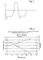
- Fig. 1shows the typical waveform used in the method of the invention.
- a half-wave with negative potentialoccurs here in each cycle a half-wave with positive potential on the target
- NiV layers whose residual stresses are above the RF power in Fig. 2were deposited on a heated substrate to which bipolar pulsed RF bias voltage was applied. There were NiV layers with a layer thickness of about 3500 A at a sputtering rate of about 15.6 A / KW sec. with a sputtering power of 9 KW with an argon flow of about 48 sccm by regular DC (DC) sputtering deposited. As in Fig. 2 can be seen, decreases with increasing RF bias power, the residual stress in the NiV layers until even build up instead of the tensile residual stress, a low compressive residual stress.
- DCDC
Landscapes
- Chemical & Material Sciences (AREA)
- Engineering & Computer Science (AREA)
- Physics & Mathematics (AREA)
- Plasma & Fusion (AREA)
- Analytical Chemistry (AREA)
- Chemical Kinetics & Catalysis (AREA)
- Materials Engineering (AREA)
- Mechanical Engineering (AREA)
- Metallurgy (AREA)
- Organic Chemistry (AREA)
- Physical Vapour Deposition (AREA)
Abstract
Description
Translated fromGermanDie vorliegende Erfindung betrifft ein Verfahren für Sputterbeschichtungsprozesse, mit denen insbesondere eigenspannungsoptmierte Beschichtungen hergestellt werden können.The present invention relates to a method for sputter coating processes, with which in particular intrinsic-stress-optimized coatings can be produced.
Aus dem Stand der Technik ist es bekannt, auf Substraten Beschichtungen durch Sputterverfahren zu erzeugen, bei denen in einer Vakuumanlage ein Plasma gezündet wird, so dass die im Plasma befindlichen Ionen durch Anlegen einer geeigneten Potentialdifferenz auf das Target, welches das zu beschichtende Material enthält, beschleunigt werden und dieses vom Target abtragen, so dass es sich auf dem zu beschichtenden Substrat ablagern kann. Die hierzu am Target einzustellende Potentialdifferenz kann entweder durch Anlegen einer Gleichspannung oder einer gepulsten Spannung erzeugt werden, wobei für den gepulsten Betrieb Frequenzen bis in den Hochfrequenzbereich (Radio frequency RF) gewählt werden können. Das Target bzw. die Sputterkathode wird hierbei jedoch üblicherweise möglichst immer auf negativem Potential oder bei bipolar gepulstem Betrieb, im positiven Pulsbereich auf lediglich niedrigem positivem Potential gehalten, da ein positiver Puls nachteilig ist, weil er dem Plasma Ladungsträger (Elektronen) entzieht. Dies ist jedoch in bestimmten Fällen in dem oben geschilderten geringen Umfang erforderlich, wenn z. B. beim Sputtern von dielektrischen Materialien sich auf dem Target eine isolierende Schicht bildet, die die kapazitiven Verhältnisse in der Beschichtungsanlage beeinträchtigt. Hier kann es dann erforderlich sein, durch Zulassen eines Überschwingens des Spannungsverlaufs ins positive Potential oder durch das Anlegen einer geringen positiven Spannung eine Entladung des Targets zu bewirken, um dadurch Aufladungserscheinungen an den isolierenden Schichten entgegen zu wirken. Aufgrund der oben geschilderten kontraproduktiven Wirkung des positiven Potentials an der Sputterkathode bzw. dem Target, wird das positive Potential jedoch nach dem Stand der Technik sehr niedrig gehalten oder wenn möglich vermieden.From the prior art, it is known to produce coatings on substrates by sputtering methods in which a plasma is ignited in a vacuum system, so that the ions present in the plasma by applying a suitable potential difference to the target containing the material to be coated, be accelerated and ablate this from the target so that it can be deposited on the substrate to be coated. The potential difference to be set on the target for this purpose can be generated either by applying a DC voltage or a pulsed voltage, wherein frequencies up to the radio frequency range (radio frequency RF) can be selected for the pulsed operation. However, the target or the sputtering cathode is usually kept as low as possible at negative potential or in bipolar pulsed operation, in the positive pulse range at only low positive potential, since a positive pulse is disadvantageous because it removes charge carriers (electrons) from the plasma. However, this is necessary in certain cases in the above-described small extent when z. B. when sputtering of dielectric materials forms an insulating layer on the target, which affects the capacitive conditions in the coating system. In this case, it may then be necessary to cause a discharge of the target by allowing an overshooting of the voltage profile into the positive potential or by applying a low positive voltage, thereby counteracting charging phenomena on the insulating layers. Due to the above-mentioned counterproductive effect of the positive potential at the sputtering cathode or the target, however, the positive potential is kept very low according to the prior art or avoided if possible.
Zur Erzeugung von möglichst eigenspannungsfreien Beschichtungen ist es im Stand der Technik weiterhin bekannt, das Substrat während der Beschichtung mit einer Bias-Spannung zu beaufschlagen ist, die ebenfalls unipolar bzw. bipolar gepulst sein kann. Durch das Anlegen einer Bias-Spannung an das Substrat wird bewirkt, dass die sich auf dem Substrat aufbauende Beschichtung mit Ionen bzw. beim bipolaren Betrieb mit Ionen und Elektronen bombardiert wird. Durch das Auftreffen der Ionen bzw. Elektronen, die durch die Bias-Spannung auf das Substrat hin beschleunigt werden, wird erreicht, dass die sich beim Abscheiden der Beschichtung möglicherweise aufbauenden Eigenspannungen durch eine gezielte Beeinflussung der Schichtstruktur bzw. des Gefüges vermindert werden. Nachteilig ist hierbei jedoch, dass durch das Beschießen des Substrats mit Ionen bzw. Elektronen das Substrat einer erhöhten Temperaturbelastung ausgesetzt ist. Außerdem wird das Beschichtungsverfahren aufwändiger, da für das Substrat eine Spannungsversorgung benötigt wird. Bei einem gepulsten Betrieb der Bias-Spannung fallen hier zusätzliche Einrichtungen an, wie z. B. Signalgeneratoren, Filter oder Synchronisierungskomponenten bei einem mit der Kathodenspannung synchron gepulsten Betrieb. Darüber hinaus sind Sputterprozesse mit einer Substrat-Bias-Spannung schwieriger zu handhaben, da sich beispielsweise die Bias-Spannung durch thermische Effekte während des Prozesses verändern kann, oder am Substrat auf Grund der Bias-Spannung beispielsweise Überschläge auftreten können.In order to generate coatings that are as free of inherent stress as possible, it is furthermore known in the state of the art to apply a bias voltage to the substrate during the coating, which can likewise be pulsed in a unipolar or bipolar manner. The application of a bias voltage to the substrate causes the coating which builds up on the substrate to be bombarded with ions or, in the case of bipolar operation, with ions and electrons. As a result of the impact of the ions or electrons, which are accelerated by the bias voltage on the substrate, it is achieved that the residual stresses possibly arising during the deposition of the coating are reduced by targeted influencing of the layer structure or of the microstructure. The disadvantage here, however, that the substrate is exposed to increased temperature stress by bombarding the substrate with ions or electrons. In addition, the coating process becomes more complex, since a voltage supply is required for the substrate. In a pulsed operation of the bias voltage here additional facilities such. As signal generators, filters or synchronization components at a synchronous pulsed with the cathode voltage operation. Moreover, sputtering processes with substrate bias voltage are more difficult to handle because, for example, the bias voltage may change due to thermal effects during the process, or, for example, arcing may occur at the substrate due to the bias voltage.
Es ist deshalb Aufgabe der vorliegenden Erfindung ein Verfahren zur Beschichtung von Substraten mittels Sputterprozessen bereitzustellen, bei denen die oben geschilderten Nachteile verringert bzw. vermieden werden können. Insbesondere soll es auch möglich sein Schichteigenschaften sowie spannungsoptimierte Schichten auf Substraten zu erzeugen, bei denen das Aufbringen einer Bias-Spannung nur unter schwierigen Bedienungen möglich oder gar gänzlich unmöglich ist, wie z. B. bei Substraten in rotierenden Substratkörben oder anderen Carriern. Bezüglich der Spannungsoptimierung der Schichten sollte es möglich sein, die insbesondere nachteiligen Zugeigenspannungen in den Schichten weitgehend zu vermindern oder zu verhindern bzw. Druckeigenspannungen in den Schichten einzustellen. Darüber hinaus soll das Verfahren einfach aufgebaut und einfach, d. h. wirtschaftlich, betreibbar sein.It is therefore an object of the present invention to provide a method for coating substrates by means of sputtering processes, in which the above-described disadvantages can be reduced or avoided. In particular, it should also be possible to produce layer properties and stress-optimized layers on substrates in which the application of a bias voltage is possible or even impossible under difficult conditions, such as. B. substrates in rotating substrate baskets or other carriers. With regard to the voltage optimization of the layers, it should be possible to largely reduce or prevent the particular disadvantageous inherent tensile stresses in the layers or to adjust residual compressive stresses in the layers. In addition, the process should be simple in design and simple, ie economical, operable.
Diese Aufgabe wird gelöst durch ein Verfahren mit Merkmalen des Patentanspruchs 1. Vorteilhafte Ausgestaltungen der Erfindung sind Gegenstand der abhängigen Ansprüche.This object is achieved by a method having features of claim 1. Advantageous embodiments of the invention are the subject of the dependent claims.
Die besonders einfache Lösung der oben geschilderten Aufgabe besteht im Wesentlichen darin, auf die Substrat-Bias-Spannung, die die oben geschilderten Nachteile mit sich bringt, gänzlich zu verzichten und dafür die nach den bisherigen Kenntnissen im Stand der Technik als nachteilig empfundene Aufbringung eines positiven Spannungspulses am Target so auszubilden, dass damit die Bias-Spannung am Substrat ersetzt werden kann. Bei entsprechender Einstellung eines positiven Potentialpulses am Target wird nämlich erreicht, dass Ionen auf das Substrat beschleunigt werden, beispielsweise positiv geladene Argon-Ionen bei Verwendung von Argon als Edelgas. Damit wird der gleiche Zweck erreicht, wie bei der Anlegung einer Substrat-Bias-Spannung, bei der ebenfalls durch Beschleunigung von Ionen aus dem Plasma auf das Substrat die Schichtstruktur so beeinflusst wird, dass negative Zugeigenspannungen abgebaut werden. Darüber hinaus werden dadurch auch sogenannte Rücksputtereffekte erzielt. Übersteigt die positive Beschleunigungsspannung für die Ionen einen Sputterschwellwert, so können anfänglich, lose gebundene Schichtatome, bei weiterer Erhöhung aus der Schicht rückgesputtert werden, was beim Beschichten von "high aspect ratio Strukturen" notwendig ist, um die Seitenwände zu beschichten.The particularly simple solution of the above-described problem is essentially to completely dispense with the substrate bias voltage, which brings the disadvantages described above, and for the according to the previous knowledge in the prior art perceived as disadvantageous application of a positive Form voltage pulse on the target so that so that the bias voltage can be replaced on the substrate. With a corresponding setting of a positive potential pulse on the target is namely achieved that ions are accelerated to the substrate, for example, positively charged argon ions using argon as a noble gas. Thus, the same purpose is achieved as in the application of a substrate bias voltage, in which also by accelerating ions from the plasma to the substrate, the layer structure is influenced so that negative residual tensile stresses are reduced. In addition, so-called backsputter effects are achieved. If the positive acceleration voltage for the ions exceeds a sputtering threshold, initially loosely bound layer atoms can be sputtered back out of the layer, which is necessary when coating "high aspect ratio structures" to coat the sidewalls.
Gegenüber einer Substrat-Bias-Spannung bewirkt das gepulste Anlegen eines positiven Potentials am Target jedoch nur einen gepulsten Beschuss des Substrats mit Ionen und keinen ununterbrochenen Beschuss mit Ionen bzw. Ionen und Elektronen. Auf diese Weise wird die Temperaturbelastung des Substrats minimiert. Außerdem ist eine gezielte Beeinflussung der Schichtstruktur auch bei Substraten möglich, bei denen das Anlegen einer Bias-Spannung Schwierigkeiten bereitet oder gar unmöglich ist. Weiterhin wird durch das Ersetzen der Bias-Spannung am Substrat durch das Vorsehen von positiven Spannungspulsen am Target auch der Aufwand für die Ausrüstung und für den Betrieb der Beschichtungseinrichtung vermindert, da keine zusätzliche Spannungsversorgung für die Bias-Spannung am Substrat vorgesehen werden muss.However, pulsed application of a positive potential to the target causes only a pulsed bombardment of the substrate with ions and no continuous bombardment with ions and electrons compared to a substrate bias voltage. In this way, the temperature load of the substrate is minimized. In addition, a targeted influencing of the layer structure is also possible with substrates in which the application of a bias voltage is difficult or even impossible. Furthermore, the replacement of the bias voltage on the substrate by the provision of positive voltage pulses at the target also reduces the outlay for the equipment and for the operation of the coating device, since no additional voltage supply for the bias voltage has to be provided on the substrate.
Hierbei ist es vorteilhaft sowohl die negative Signalgrundform für das Spannungssignal an der Sputterkathode bzw. am Target als auch das positive Spannungssignal für das erfindungsgemäße Verfahren durch einen Signalgenerator am Target zu erzeugen. Auf diese Weise kann die Sputterbeschichtungsvorrichtung vereinfacht und der Betrieb weniger aufwändig gestaltet werden.In this case, it is advantageous to generate both the negative signal basic form for the voltage signal at the sputtering cathode or at the target and also the positive voltage signal for the method according to the invention by a signal generator at the target. In this way, the sputter coating apparatus can be simplified and the operation can be made less expensive.
Um jedoch das gepulste positive Spannungssignal am Target hinsichtlich Frequenz, Signalform, Amplitude usw. möglichst frei einstellen zu können, ist es jedoch bevorzugt, das Spannungssignal an der Sputterkathode bzw. am Target durch die Überlagerung einer negativen Signalgrundform mit einem gepulsten positiven Spannungsignal zu erzeugen.However, in order to be able to set the pulsed positive voltage signal as freely as possible with respect to frequency, signal shape, amplitude, etc., it is preferred to generate the voltage signal at the sputtering cathode or at the target by superposing a negative signal basic form with a pulsed positive voltage signal.
Bei der Herstellung verschiedener Schichten mit dem erfindungsgemäßen Verfahren hat es sich herausgestellt, dass es besonders vorteilhaft ist, wenn die Amplitude des positiven Spannungspulses im Bereich von 30 bis 2000 V, insbesondere 40 bis 1800V, vorzugsweise 50 bis 1000 V, und/ oder die Pulsdauer des positiven Spannungspulses im Bereich von 1 bis 20 µsec gewählt wird. Außerdem hat sich eine Frequenz von 15 bis 450 KHz bewährt.In the production of various layers with the method according to the invention it has been found that it is particularly advantageous if the amplitude of the positive voltage pulse in the range of 30 to 2000 V, in particular 40 to 1800V, preferably 50 to 1000 V, and / or the pulse duration the positive voltage pulse in the range of 1 to 20 μsec is selected. In addition, a frequency of 15 to 450 KHz has been proven.
Weitere Vorteile, Kennzeichen und Merkmale der vorliegenden Erfindung werden bei der nachfolgenden detaillierten Beschreibung eines Vergleichsbeispiels deutlich. Hierbei zeigen die beigefügten Diagramme in
- Fig. 1
- einen typischen Verlauf des Potentials am Target;
- Fig. 2
- die Eigenspannungsreduzierung bzw. Erhöhung des spezifischen Widerstands bei Schichten, die mit hochfrequenter Bias-Spannung abgeschieden worden sind; und in
- Fig. 3
- die Verringerung bzw. Umkehrung der Eigenspannungen in Schichten, die mit dem erfindungsgemäßen Verfahren abgeschieden worden sind.
- Fig. 1
- a typical course of the potential at the target;
- Fig. 2
- the residual stress reduction or increase in the specific resistance in layers which have been deposited with high-frequency bias voltage; and in
- Fig. 3
- the reduction or reversal of the residual stresses in layers which have been deposited by the method according to the invention.
Bei dem vorliegenden Vergleichsbeispiel wird die Beeinflussung der Eigenspannungen in NiV-Schichten durch Anlegen einer RF-Bias-Spannung an das Substrat während des Abscheidens mit der Eigenspannungsentwicklung in NiV-Schichten verglichen, die mit unterschiedlichen positiven Spannungspulsen nach dem erfindungsgemäßen Verfahren abgeschieden worden sind.
Beim Vergleich der Eigenspannungen innerhalb der NiV-Schichten, die einerseits mit einem Verfahren nach dem Stand der Technik (
Die NiV-Schichten, deren Eigenspannungen über der RF-Leistung in
Diese positive Wirkung wurde nun bei den NiV-Schichten, die mit dem erfindungsgemäßen Verfahren hergestellt wurden, auch ohne Verwendung einer Bias-Spannung erzeugt, und zwar durch Verwendung des erfindungsgemäßen bipolaren Pulses am Target (vgl.
Claims (5)
- A method for producing coatings with optimized internal stress, in particular with low internal tensile stress, through sputtering processes, wherein a bipolar-pulsed voltage curve is generated at a target (cathode), wherein a positive voltage pulse at the target is adjusted, so that ions are accelerated towards a substrate and impact the coating due to the acceleration.
- The method according to claim, 1 wherein the positive voltage pulse is generated through superimposing a negative basic signal curve with a pulsed positive voltage signal, wherein the pulsed positive pulse voltage signal is adjustable with respect to frequency, signal form, amplitude and similar.
- The method according to claim 1 or 2, wherein the positive voltage pulse comprises an amplitude of 30 to 2,000 V, in particular 40 to 1,800 V, preferably 50 to 1,000 V.
- The method according to one of the preceding claims, wherein the positive voltage pulse comprises a pulse duration of 1 to 20 µs.
- The method according to one of the preceding claims, wherein the positive voltage pulse is applied with a frequency of 15 to 450 kHz.
Applications Claiming Priority (3)
| Application Number | Priority Date | Filing Date | Title |
|---|---|---|---|
| DE10222909ADE10222909A1 (en) | 2002-05-22 | 2002-05-22 | Sputtering process or device for the production of coatings optimized for residual stress |
| DE10222909 | 2002-05-22 | ||
| PCT/EP2003/004572WO2003097896A1 (en) | 2002-05-22 | 2003-04-30 | Sputter method or device for the production of natural voltage optimized coatings |
Publications (2)
| Publication Number | Publication Date |
|---|---|
| EP1511877A1 EP1511877A1 (en) | 2005-03-09 |
| EP1511877B1true EP1511877B1 (en) | 2010-09-15 |
Family
ID=29414081
Family Applications (1)
| Application Number | Title | Priority Date | Filing Date |
|---|---|---|---|
| EP03752719AExpired - LifetimeEP1511877B1 (en) | 2002-05-22 | 2003-04-30 | Sputter method for the production of natural voltage optimized coatings |
Country Status (9)
| Country | Link |
|---|---|
| US (1) | US20070009670A9 (en) |
| EP (1) | EP1511877B1 (en) |
| JP (1) | JP2005534803A (en) |
| CN (1) | CN100577855C (en) |
| AT (1) | ATE481511T1 (en) |
| AU (1) | AU2003232242A1 (en) |
| DE (2) | DE10222909A1 (en) |
| TW (1) | TWI275655B (en) |
| WO (1) | WO2003097896A1 (en) |
Cited By (1)
| Publication number | Priority date | Publication date | Assignee | Title |
|---|---|---|---|---|
| WO2014001525A1 (en) | 2012-06-29 | 2014-01-03 | Oc Oerlikon Balzers Ag | Method of coating by pulsed bipolar sputtering |
Families Citing this family (8)
| Publication number | Priority date | Publication date | Assignee | Title |
|---|---|---|---|---|
| US20060278521A1 (en)* | 2005-06-14 | 2006-12-14 | Stowell Michael W | System and method for controlling ion density and energy using modulated power signals |
| KR101046520B1 (en) | 2007-09-07 | 2011-07-04 | 어플라이드 머티어리얼스, 인코포레이티드 | Source gas flow path control in pecvd system to control a by-product film deposition on inside chamber |
| DE102008060838A1 (en) | 2008-12-05 | 2010-06-10 | Zounek, Alexis, Dr. | Coating substrates, comprises generating plasma with positively charged ion that is accelerated on substrate by negative bias potential, and reducing and/or compensating positive loading of substrate by irradiating substrate with electron |
| US12297529B1 (en) | 2010-05-19 | 2025-05-13 | Corporation For National Research Initiatives | Method and system for controlling the state of stress in deposited thin films |
| DE102010034321B4 (en)* | 2010-08-09 | 2017-04-06 | Technische Universität Dresden | Process for the production of a hard material coating on metallic, ceramic or hard metallic components as well as a hard material coating produced by the process |
| US8252680B2 (en)* | 2010-09-24 | 2012-08-28 | Intel Corporation | Methods and architectures for bottomless interconnect vias |
| US9399812B2 (en)* | 2011-10-11 | 2016-07-26 | Applied Materials, Inc. | Methods of preventing plasma induced damage during substrate processing |
| JP2021021120A (en)* | 2019-07-29 | 2021-02-18 | 株式会社アルバック | Sputtering method and sputtering apparatus |
Family Cites Families (15)
| Publication number | Priority date | Publication date | Assignee | Title |
|---|---|---|---|---|
| JPH06145975A (en)* | 1992-03-20 | 1994-05-27 | Komag Inc | Method of spattering carbon film and its product |
| JP2711503B2 (en)* | 1993-07-07 | 1998-02-10 | アネルバ株式会社 | Thin film formation method by bias sputtering |
| DE4401986A1 (en)* | 1994-01-25 | 1995-07-27 | Dresden Vakuumtech Gmbh | Method for operating a vacuum arc evaporator and power supply device therefor |
| JPH07224379A (en)* | 1994-02-14 | 1995-08-22 | Ulvac Japan Ltd | Sputtering method and device therefor |
| JPH07243039A (en)* | 1994-03-02 | 1995-09-19 | Chugai Ro Co Ltd | Dc-magnetron reactive sputtering method |
| JP3720061B2 (en)* | 1994-03-24 | 2005-11-24 | 株式会社アルバック | DC sputtering film forming method for thin film resistors |
| JP3585519B2 (en)* | 1994-03-25 | 2004-11-04 | 株式会社アルバック | Sputtering apparatus and sputtering method |
| US5651865A (en)* | 1994-06-17 | 1997-07-29 | Eni | Preferential sputtering of insulators from conductive targets |
| JP2904263B2 (en)* | 1995-12-04 | 1999-06-14 | 日本電気株式会社 | Sputtering equipment |
| US5770023A (en)* | 1996-02-12 | 1998-06-23 | Eni A Division Of Astec America, Inc. | Etch process employing asymmetric bipolar pulsed DC |
| DE19651811B4 (en)* | 1996-12-13 | 2006-08-31 | Unaxis Deutschland Holding Gmbh | Device for covering a substrate with thin layers |
| US6086830A (en)* | 1997-09-23 | 2000-07-11 | Imperial Petroleum Recovery Corporation | Radio frequency microwave energy applicator apparatus to break oil and water emulsion |
| US6149778A (en)* | 1998-03-12 | 2000-11-21 | Lucent Technologies Inc. | Article comprising fluorinated amorphous carbon and method for fabricating article |
| US6620720B1 (en)* | 2000-04-10 | 2003-09-16 | Agere Systems Inc | Interconnections to copper IC's |
| US6506289B2 (en)* | 2000-08-07 | 2003-01-14 | Symmorphix, Inc. | Planar optical devices and methods for their manufacture |
- 2002
- 2002-05-22DEDE10222909Apatent/DE10222909A1/ennot_activeWithdrawn
- 2003
- 2003-04-30AUAU2003232242Apatent/AU2003232242A1/ennot_activeAbandoned
- 2003-04-30JPJP2004505408Apatent/JP2005534803A/enactivePending
- 2003-04-30CNCN03811588Apatent/CN100577855C/ennot_activeExpired - Fee Related
- 2003-04-30ATAT03752719Tpatent/ATE481511T1/enactive
- 2003-04-30USUS10/515,792patent/US20070009670A9/ennot_activeAbandoned
- 2003-04-30WOPCT/EP2003/004572patent/WO2003097896A1/enactiveApplication Filing
- 2003-04-30DEDE50313095Tpatent/DE50313095D1/ennot_activeExpired - Lifetime
- 2003-04-30EPEP03752719Apatent/EP1511877B1/ennot_activeExpired - Lifetime
- 2003-05-22TWTW092113899Apatent/TWI275655B/ennot_activeIP Right Cessation
Cited By (1)
| Publication number | Priority date | Publication date | Assignee | Title |
|---|---|---|---|---|
| WO2014001525A1 (en) | 2012-06-29 | 2014-01-03 | Oc Oerlikon Balzers Ag | Method of coating by pulsed bipolar sputtering |
Also Published As
| Publication number | Publication date |
|---|---|
| EP1511877A1 (en) | 2005-03-09 |
| WO2003097896A1 (en) | 2003-11-27 |
| TW200406500A (en) | 2004-05-01 |
| TWI275655B (en) | 2007-03-11 |
| CN100577855C (en) | 2010-01-06 |
| JP2005534803A (en) | 2005-11-17 |
| US20070009670A9 (en) | 2007-01-11 |
| ATE481511T1 (en) | 2010-10-15 |
| DE10222909A1 (en) | 2003-12-04 |
| CN1656244A (en) | 2005-08-17 |
| AU2003232242A1 (en) | 2003-12-02 |
| US20050233089A1 (en) | 2005-10-20 |
| DE50313095D1 (en) | 2010-10-28 |
Similar Documents
| Publication | Publication Date | Title |
|---|---|---|
| DE3852912T2 (en) | Sputtering method and apparatus. | |
| DE3700633C1 (en) | Method and device for the gentle coating of electrically conductive objects by means of plasma | |
| DE69318856T2 (en) | Coated moldings | |
| DE102008021912C5 (en) | coating process | |
| EP0182889B1 (en) | Method for producing diamond-like carbon layers | |
| EP2159821B1 (en) | Coating device for coating a substrate and method for same | |
| EP2777061B1 (en) | Hipims-layers | |
| EP3017078B1 (en) | Tib2 layers and their preparation | |
| EP1511877B1 (en) | Sputter method for the production of natural voltage optimized coatings | |
| EP2789006B1 (en) | Reactive sputtering process | |
| WO2015007466A1 (en) | Method for depositing a piezoelectric film containing ain, and a piezoelectric film containing ain | |
| EP0666335B1 (en) | Method for operation of a vacuum arc evaporator and current supply therefor | |
| EP2175044B1 (en) | PVD coating method, device for carrying out the procedure and substances coated with the procedure | |
| EP0404973A1 (en) | Process and apparatus for coating substrates | |
| EP2439763A2 (en) | Magentron device and method for pulsed operation of a magnetron device | |
| DE102016116762B4 (en) | Method for depositing a layer by means of a magnetron sputtering device | |
| EP2286643B1 (en) | Device and method for high-performance pulsed gas flow sputtering | |
| DE112010005558B4 (en) | Apparatus and method for gas flow sputtering | |
| EP2300631B1 (en) | Method for producing a transparent and conductive metal oxide layer by highly ionized pulsed magnetron sputtering | |
| DE19911046B4 (en) | plasma process | |
| DE102009019422B4 (en) | Method for generating a plasma by means of a magnetron | |
| DE102012107163A1 (en) | Coating a substrate using high energy pulse magnetron sputtering, comprises applying bipolar pulses on at least one aluminum containing magnetron target for producing an aluminum oxide coating, and coating without external heat supply | |
| DE102010007516A1 (en) | Large-scale cathode for magnetron sputtering within vacuum chamber, comprises target, and device for producing a magnetic field, which is enclosed itself on the surface of the target in circular manner and is formed in tunnel-shaped manner | |
| EP1473382A1 (en) | Process and apparatus for plasma-activated film deposition by magnetron sputtering | |
| WO2014202648A1 (en) | Method for pretreating a surface to be coated |
Legal Events
| Date | Code | Title | Description |
|---|---|---|---|
| PUAI | Public reference made under article 153(3) epc to a published international application that has entered the european phase | Free format text:ORIGINAL CODE: 0009012 | |
| 17P | Request for examination filed | Effective date:20041210 | |
| AK | Designated contracting states | Kind code of ref document:A1 Designated state(s):AT BE BG CH CY CZ DE DK EE ES FI FR GB GR HU IE IT LI LU MC NL PT RO SE SI SK TR | |
| AX | Request for extension of the european patent | Extension state:AL LT LV MK | |
| 17Q | First examination report despatched | Effective date:20050427 | |
| RIN1 | Information on inventor provided before grant (corrected) | Inventor name:HAAG, WALTER | |
| DAX | Request for extension of the european patent (deleted) | ||
| RAP1 | Party data changed (applicant data changed or rights of an application transferred) | Owner name:OC OERLIKON BALZERS AG | |
| GRAP | Despatch of communication of intention to grant a patent | Free format text:ORIGINAL CODE: EPIDOSNIGR1 | |
| RTI1 | Title (correction) | Free format text:SPUTTER METHOD FOR THE PRODUCTION OF NATURAL VOLTAGE OPTIMIZED COATINGS | |
| GRAS | Grant fee paid | Free format text:ORIGINAL CODE: EPIDOSNIGR3 | |
| GRAA | (expected) grant | Free format text:ORIGINAL CODE: 0009210 | |
| AK | Designated contracting states | Kind code of ref document:B1 Designated state(s):AT BE BG CH CY CZ DE DK EE ES FI FR GB GR HU IE IT LI LU MC NL PT RO SE SI SK TR | |
| REG | Reference to a national code | Ref country code:GB Ref legal event code:FG4D Free format text:NOT ENGLISH Ref country code:CH Ref legal event code:EP | |
| REG | Reference to a national code | Ref country code:IE Ref legal event code:FG4D Free format text:LANGUAGE OF EP DOCUMENT: GERMAN | |
| REF | Corresponds to: | Ref document number:50313095 Country of ref document:DE Date of ref document:20101028 Kind code of ref document:P | |
| REG | Reference to a national code | Ref country code:NL Ref legal event code:VDEP Effective date:20100915 | |
| PG25 | Lapsed in a contracting state [announced via postgrant information from national office to epo] | Ref country code:FI Free format text:LAPSE BECAUSE OF FAILURE TO SUBMIT A TRANSLATION OF THE DESCRIPTION OR TO PAY THE FEE WITHIN THE PRESCRIBED TIME-LIMIT Effective date:20100915 | |
| PG25 | Lapsed in a contracting state [announced via postgrant information from national office to epo] | Ref country code:SI Free format text:LAPSE BECAUSE OF FAILURE TO SUBMIT A TRANSLATION OF THE DESCRIPTION OR TO PAY THE FEE WITHIN THE PRESCRIBED TIME-LIMIT Effective date:20100915 Ref country code:CY Free format text:LAPSE BECAUSE OF FAILURE TO SUBMIT A TRANSLATION OF THE DESCRIPTION OR TO PAY THE FEE WITHIN THE PRESCRIBED TIME-LIMIT Effective date:20100915 | |
| PG25 | Lapsed in a contracting state [announced via postgrant information from national office to epo] | Ref country code:GR Free format text:LAPSE BECAUSE OF FAILURE TO SUBMIT A TRANSLATION OF THE DESCRIPTION OR TO PAY THE FEE WITHIN THE PRESCRIBED TIME-LIMIT Effective date:20101216 Ref country code:SE Free format text:LAPSE BECAUSE OF FAILURE TO SUBMIT A TRANSLATION OF THE DESCRIPTION OR TO PAY THE FEE WITHIN THE PRESCRIBED TIME-LIMIT Effective date:20100915 | |
| PG25 | Lapsed in a contracting state [announced via postgrant information from national office to epo] | Ref country code:SK Free format text:LAPSE BECAUSE OF FAILURE TO SUBMIT A TRANSLATION OF THE DESCRIPTION OR TO PAY THE FEE WITHIN THE PRESCRIBED TIME-LIMIT Effective date:20100915 Ref country code:PT Free format text:LAPSE BECAUSE OF FAILURE TO SUBMIT A TRANSLATION OF THE DESCRIPTION OR TO PAY THE FEE WITHIN THE PRESCRIBED TIME-LIMIT Effective date:20110117 Ref country code:RO Free format text:LAPSE BECAUSE OF FAILURE TO SUBMIT A TRANSLATION OF THE DESCRIPTION OR TO PAY THE FEE WITHIN THE PRESCRIBED TIME-LIMIT Effective date:20100915 Ref country code:EE Free format text:LAPSE BECAUSE OF FAILURE TO SUBMIT A TRANSLATION OF THE DESCRIPTION OR TO PAY THE FEE WITHIN THE PRESCRIBED TIME-LIMIT Effective date:20100915 Ref country code:CZ Free format text:LAPSE BECAUSE OF FAILURE TO SUBMIT A TRANSLATION OF THE DESCRIPTION OR TO PAY THE FEE WITHIN THE PRESCRIBED TIME-LIMIT Effective date:20100915 Ref country code:NL Free format text:LAPSE BECAUSE OF FAILURE TO SUBMIT A TRANSLATION OF THE DESCRIPTION OR TO PAY THE FEE WITHIN THE PRESCRIBED TIME-LIMIT Effective date:20100915 | |
| PG25 | Lapsed in a contracting state [announced via postgrant information from national office to epo] | Ref country code:ES Free format text:LAPSE BECAUSE OF FAILURE TO SUBMIT A TRANSLATION OF THE DESCRIPTION OR TO PAY THE FEE WITHIN THE PRESCRIBED TIME-LIMIT Effective date:20101226 | |
| PLBE | No opposition filed within time limit | Free format text:ORIGINAL CODE: 0009261 | |
| STAA | Information on the status of an ep patent application or granted ep patent | Free format text:STATUS: NO OPPOSITION FILED WITHIN TIME LIMIT | |
| 26N | No opposition filed | Effective date:20110616 | |
| PG25 | Lapsed in a contracting state [announced via postgrant information from national office to epo] | Ref country code:DK Free format text:LAPSE BECAUSE OF FAILURE TO SUBMIT A TRANSLATION OF THE DESCRIPTION OR TO PAY THE FEE WITHIN THE PRESCRIBED TIME-LIMIT Effective date:20100915 | |
| REG | Reference to a national code | Ref country code:DE Ref legal event code:R097 Ref document number:50313095 Country of ref document:DE Effective date:20110616 | |
| BERE | Be: lapsed | Owner name:OC OERLIKON BALZERS AG Effective date:20110430 | |
| PG25 | Lapsed in a contracting state [announced via postgrant information from national office to epo] | Ref country code:MC Free format text:LAPSE BECAUSE OF NON-PAYMENT OF DUE FEES Effective date:20110430 | |
| PG25 | Lapsed in a contracting state [announced via postgrant information from national office to epo] | Ref country code:BE Free format text:LAPSE BECAUSE OF NON-PAYMENT OF DUE FEES Effective date:20110430 | |
| REG | Reference to a national code | Ref country code:AT Ref legal event code:MM01 Ref document number:481511 Country of ref document:AT Kind code of ref document:T Effective date:20110430 | |
| PG25 | Lapsed in a contracting state [announced via postgrant information from national office to epo] | Ref country code:AT Free format text:LAPSE BECAUSE OF NON-PAYMENT OF DUE FEES Effective date:20110430 | |
| PG25 | Lapsed in a contracting state [announced via postgrant information from national office to epo] | Ref country code:LU Free format text:LAPSE BECAUSE OF NON-PAYMENT OF DUE FEES Effective date:20110430 | |
| PG25 | Lapsed in a contracting state [announced via postgrant information from national office to epo] | Ref country code:TR Free format text:LAPSE BECAUSE OF FAILURE TO SUBMIT A TRANSLATION OF THE DESCRIPTION OR TO PAY THE FEE WITHIN THE PRESCRIBED TIME-LIMIT Effective date:20100915 Ref country code:BG Free format text:LAPSE BECAUSE OF FAILURE TO SUBMIT A TRANSLATION OF THE DESCRIPTION OR TO PAY THE FEE WITHIN THE PRESCRIBED TIME-LIMIT Effective date:20101215 | |
| PG25 | Lapsed in a contracting state [announced via postgrant information from national office to epo] | Ref country code:HU Free format text:LAPSE BECAUSE OF FAILURE TO SUBMIT A TRANSLATION OF THE DESCRIPTION OR TO PAY THE FEE WITHIN THE PRESCRIBED TIME-LIMIT Effective date:20100915 | |
| REG | Reference to a national code | Ref country code:CH Ref legal event code:PFA Owner name:OERLIKON ADVANCED TECHNOLOGIES AG, LI Free format text:FORMER OWNER: OC OERLIKON BALZERS AG, LI | |
| REG | Reference to a national code | Ref country code:FR Ref legal event code:TP Owner name:OERLIKON ADVANCED TECHNOLOGIES AG, LI Effective date:20140627 | |
| REG | Reference to a national code | Ref country code:GB Ref legal event code:732E Free format text:REGISTERED BETWEEN 20140710 AND 20140716 | |
| REG | Reference to a national code | Ref country code:DE Ref legal event code:R081 Ref document number:50313095 Country of ref document:DE Owner name:OERLIKON ADVANCED TECHNOLOGIES AG, LI Free format text:FORMER OWNER: OC OERLIKON BALZERS AG, BALZERS, LI Effective date:20141216 | |
| REG | Reference to a national code | Ref country code:FR Ref legal event code:PLFP Year of fee payment:14 | |
| REG | Reference to a national code | Ref country code:FR Ref legal event code:PLFP Year of fee payment:15 | |
| REG | Reference to a national code | Ref country code:FR Ref legal event code:PLFP Year of fee payment:16 | |
| REG | Reference to a national code | Ref country code:CH Ref legal event code:PUE Owner name:EVATEC AG, CH Free format text:FORMER OWNER: OERLIKON ADVANCED TECHNOLOGIES AG, LI | |
| REG | Reference to a national code | Ref country code:DE Ref legal event code:R081 Ref document number:50313095 Country of ref document:DE Owner name:EVATEC AG, CH Free format text:FORMER OWNER: OERLIKON ADVANCED TECHNOLOGIES AG, BALZERS, LI | |
| REG | Reference to a national code | Ref country code:DE Ref legal event code:R081 Ref document number:50313095 Country of ref document:DE Owner name:EVATEC AG, CH Free format text:FORMER OWNER: EVATEC ADVANCED TECHNOLOGIES AG, BALZERS, LI | |
| REG | Reference to a national code | Ref country code:GB Ref legal event code:732E Free format text:REGISTERED BETWEEN 20200514 AND 20200520 | |
| PGFP | Annual fee paid to national office [announced via postgrant information from national office to epo] | Ref country code:CH Payment date:20200407 Year of fee payment:18 Ref country code:IE Payment date:20200409 Year of fee payment:18 | |
| PGFP | Annual fee paid to national office [announced via postgrant information from national office to epo] | Ref country code:GB Payment date:20200422 Year of fee payment:18 Ref country code:IT Payment date:20200312 Year of fee payment:18 | |
| PGFP | Annual fee paid to national office [announced via postgrant information from national office to epo] | Ref country code:FR Payment date:20210310 Year of fee payment:19 | |
| PGFP | Annual fee paid to national office [announced via postgrant information from national office to epo] | Ref country code:DE Payment date:20210408 Year of fee payment:19 | |
| GBPC | Gb: european patent ceased through non-payment of renewal fee | Effective date:20210430 | |
| PG25 | Lapsed in a contracting state [announced via postgrant information from national office to epo] | Ref country code:GB Free format text:LAPSE BECAUSE OF NON-PAYMENT OF DUE FEES Effective date:20210430 Ref country code:LI Free format text:LAPSE BECAUSE OF NON-PAYMENT OF DUE FEES Effective date:20210430 Ref country code:CH Free format text:LAPSE BECAUSE OF NON-PAYMENT OF DUE FEES Effective date:20210430 | |
| PG25 | Lapsed in a contracting state [announced via postgrant information from national office to epo] | Ref country code:IE Free format text:LAPSE BECAUSE OF NON-PAYMENT OF DUE FEES Effective date:20210430 | |
| REG | Reference to a national code | Ref country code:DE Ref legal event code:R119 Ref document number:50313095 Country of ref document:DE | |
| PG25 | Lapsed in a contracting state [announced via postgrant information from national office to epo] | Ref country code:FR Free format text:LAPSE BECAUSE OF NON-PAYMENT OF DUE FEES Effective date:20220430 Ref country code:DE Free format text:LAPSE BECAUSE OF NON-PAYMENT OF DUE FEES Effective date:20221103 | |
| PG25 | Lapsed in a contracting state [announced via postgrant information from national office to epo] | Ref country code:IT Free format text:LAPSE BECAUSE OF NON-PAYMENT OF DUE FEES Effective date:20200430 |