EP1508906A2 - Capacitor, method of manufacturing the same and memory device including the same - Google Patents
Capacitor, method of manufacturing the same and memory device including the sameDownload PDFInfo
- Publication number
- EP1508906A2 EP1508906A2EP04254930AEP04254930AEP1508906A2EP 1508906 A2EP1508906 A2EP 1508906A2EP 04254930 AEP04254930 AEP 04254930AEP 04254930 AEP04254930 AEP 04254930AEP 1508906 A2EP1508906 A2EP 1508906A2
- Authority
- EP
- European Patent Office
- Prior art keywords
- oxide film
- film
- capacitor
- forming
- lower electrode
- Prior art date
- Legal status (The legal status is an assumption and is not a legal conclusion. Google has not performed a legal analysis and makes no representation as to the accuracy of the status listed.)
- Withdrawn
Links
Images

Classifications
- H—ELECTRICITY
- H10—SEMICONDUCTOR DEVICES; ELECTRIC SOLID-STATE DEVICES NOT OTHERWISE PROVIDED FOR
- H10B—ELECTRONIC MEMORY DEVICES
- H10B12/00—Dynamic random access memory [DRAM] devices
- H—ELECTRICITY
- H10—SEMICONDUCTOR DEVICES; ELECTRIC SOLID-STATE DEVICES NOT OTHERWISE PROVIDED FOR
- H10D—INORGANIC ELECTRIC SEMICONDUCTOR DEVICES
- H10D1/00—Resistors, capacitors or inductors
- H10D1/60—Capacitors
- H10D1/68—Capacitors having no potential barriers
- H—ELECTRICITY
- H01—ELECTRIC ELEMENTS
- H01G—CAPACITORS; CAPACITORS, RECTIFIERS, DETECTORS, SWITCHING DEVICES, LIGHT-SENSITIVE OR TEMPERATURE-SENSITIVE DEVICES OF THE ELECTROLYTIC TYPE
- H01G4/00—Fixed capacitors; Processes of their manufacture
- H01G4/002—Details
- H01G4/018—Dielectrics
- H01G4/06—Solid dielectrics
- H01G4/08—Inorganic dielectrics
- H01G4/10—Metal-oxide dielectrics
- H—ELECTRICITY
- H01—ELECTRIC ELEMENTS
- H01G—CAPACITORS; CAPACITORS, RECTIFIERS, DETECTORS, SWITCHING DEVICES, LIGHT-SENSITIVE OR TEMPERATURE-SENSITIVE DEVICES OF THE ELECTROLYTIC TYPE
- H01G4/00—Fixed capacitors; Processes of their manufacture
- H01G4/002—Details
- H01G4/018—Dielectrics
- H01G4/06—Solid dielectrics
- H01G4/08—Inorganic dielectrics
- H01G4/12—Ceramic dielectrics
- H01G4/1272—Semiconductive ceramic capacitors
- H—ELECTRICITY
- H10—SEMICONDUCTOR DEVICES; ELECTRIC SOLID-STATE DEVICES NOT OTHERWISE PROVIDED FOR
- H10B—ELECTRONIC MEMORY DEVICES
- H10B51/00—Ferroelectric RAM [FeRAM] devices comprising ferroelectric memory transistors
- H—ELECTRICITY
- H10—SEMICONDUCTOR DEVICES; ELECTRIC SOLID-STATE DEVICES NOT OTHERWISE PROVIDED FOR
- H10B—ELECTRONIC MEMORY DEVICES
- H10B51/00—Ferroelectric RAM [FeRAM] devices comprising ferroelectric memory transistors
- H10B51/30—Ferroelectric RAM [FeRAM] devices comprising ferroelectric memory transistors characterised by the memory core region
- H—ELECTRICITY
- H10—SEMICONDUCTOR DEVICES; ELECTRIC SOLID-STATE DEVICES NOT OTHERWISE PROVIDED FOR
- H10B—ELECTRONIC MEMORY DEVICES
- H10B53/00—Ferroelectric RAM [FeRAM] devices comprising ferroelectric memory capacitors
- H—ELECTRICITY
- H01—ELECTRIC ELEMENTS
- H01L—SEMICONDUCTOR DEVICES NOT COVERED BY CLASS H10
- H01L21/00—Processes or apparatus adapted for the manufacture or treatment of semiconductor or solid state devices or of parts thereof
- H01L21/02—Manufacture or treatment of semiconductor devices or of parts thereof
- H01L21/02104—Forming layers
- H01L21/02107—Forming insulating materials on a substrate
- H01L21/02109—Forming insulating materials on a substrate characterised by the type of layer, e.g. type of material, porous/non-porous, pre-cursors, mixtures or laminates
- H01L21/022—Forming insulating materials on a substrate characterised by the type of layer, e.g. type of material, porous/non-porous, pre-cursors, mixtures or laminates the layer being a laminate, i.e. composed of sublayers, e.g. stacks of alternating high-k metal oxides
- H—ELECTRICITY
- H01—ELECTRIC ELEMENTS
- H01L—SEMICONDUCTOR DEVICES NOT COVERED BY CLASS H10
- H01L21/00—Processes or apparatus adapted for the manufacture or treatment of semiconductor or solid state devices or of parts thereof
- H01L21/02—Manufacture or treatment of semiconductor devices or of parts thereof
- H01L21/02104—Forming layers
- H01L21/02107—Forming insulating materials on a substrate
- H01L21/02225—Forming insulating materials on a substrate characterised by the process for the formation of the insulating layer
- H01L21/0226—Forming insulating materials on a substrate characterised by the process for the formation of the insulating layer formation by a deposition process
- H01L21/02263—Forming insulating materials on a substrate characterised by the process for the formation of the insulating layer formation by a deposition process deposition from the gas or vapour phase
- H01L21/02271—Forming insulating materials on a substrate characterised by the process for the formation of the insulating layer formation by a deposition process deposition from the gas or vapour phase deposition by decomposition or reaction of gaseous or vapour phase compounds, i.e. chemical vapour deposition
- H01L21/0228—Forming insulating materials on a substrate characterised by the process for the formation of the insulating layer formation by a deposition process deposition from the gas or vapour phase deposition by decomposition or reaction of gaseous or vapour phase compounds, i.e. chemical vapour deposition deposition by cyclic CVD, e.g. ALD, ALE, pulsed CVD
- H—ELECTRICITY
- H10—SEMICONDUCTOR DEVICES; ELECTRIC SOLID-STATE DEVICES NOT OTHERWISE PROVIDED FOR
- H10D—INORGANIC ELECTRIC SEMICONDUCTOR DEVICES
- H10D1/00—Resistors, capacitors or inductors
- H10D1/60—Capacitors
- H10D1/68—Capacitors having no potential barriers
- H10D1/682—Capacitors having no potential barriers having dielectrics comprising perovskite structures
- H10D1/684—Capacitors having no potential barriers having dielectrics comprising perovskite structures the dielectrics comprising multiple layers, e.g. comprising buffer layers, seed layers or gradient layers
Definitions
- the present inventionrelates to a semiconductor device and a method of manufacturing the same, and more particularly, to a capacitor, a method of manufacturing the same and a memory device including the capacitor.
- a lanthanum oxide (La 2 O 3 )can be used as a dielectric film in a capacitor of a semiconductor device.
- silicateWhen a lanthanum oxide film is deposited on a silicon layer, a silicate is formed in the capacitor as a result of a reaction between the lanthanum oxide film and silicon of the silicon layer. The formation of silicate results in lowering characteristics of the capacitor.
- the capacitance of a capacitoris proportional to a surface area of an electrode. Therefore, the capacitance of a capacitor can be increased by forming the electrode in three dimensions.
- a thickness and a composition of a dielectric filmare uniform even if the electrode of the capacitor has a complicated structure.
- a conventional deposition methodsuch as a chemical vapor deposition (CVD) method is not suitable for forming a dielectric film having a uniform thickness and composition on an electrode with a complicated structure due to process characteristics of the CVD method.
- CVDchemical vapor deposition
- ALDatomic layer deposition
- the ALD methodcan be used for forming a dielectric film having a uniform thickness and composition on a capacitor electrode having a complicated structure.
- the lanthanum oxide filmcan also be formed using the ALD method.
- ALD methodthere is a possibility of characteristic changes of the lanthanum oxide film resulting from absorption of water vapor (H 2 O) when the lanthanum oxide is exposed to the air because lanthanides are hygroscopic.
- a large amount of water vaporcan be absorbed by the lanthanum precursor layer during an oxidization process using water vapor (H 2 O).
- electrical characteristicssuch as an ability of the lanthanum oxide film to prevent a leakage current can be degraded.
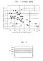
- FIG. 1is a graph illustrating the increase in the leakage current density when water vapor is used as an oxidation gas for forming a few oxide films such as the lanthanum oxide film using the ALD method.
- Reference character B1represents a leakage current density of an aluminum oxide film formed to a thickness of 40 ⁇
- B2represents that of a hafnium oxide film formed in a thickness of 45 ⁇ .
- Reference character B3, B4, and B5represent leakage currents of precursors La(tmhd) 3 , La(N(Si(Me) 3 ) 2 ) 3 , and La(iPrCp) 3 , respectively.
- a capacitor of a semiconductor devicecomprising a lower electrode, a dielectric film, and an upper electrode with a first reaction barrier film formed between the lower electrode and the dielectric film.
- the dielectric filmis an oxide film that includes a lanthanide element.
- a second reaction barrier filmcan further be formed between the upper electrode and the dielectric film.
- the first and second reaction barrier filmsare each a hafnium oxide film or an aluminum oxide film that includes positive ions with smaller radii than positive ions of the lanthanum oxide film (La 2 O 3 ).
- a method of forming a capacitorcomprising forming a lower electrode, forming a first reaction barrier film on the lower electrode, forming a precursor layer that includes a metal element on the first reaction barrier film, forming an oxide film that includes a metal element by oxidizing the metal element of the precursor layer, drying the oxide film, and forming an upper electrode on the dried oxide film.
- the lower electrodeis a silicon electrode doped with a conductive dopant
- the upper electrodeis a titanium nitride film.
- a second reaction barrier filmcan further be formed between the dried oxide film and the upper electrode, and the lower electrode and the upper electrode can be silicon electrodes doped with a conductive dopant or titanium nitride films.
- An exhaust processmay be performed after forming the precursor layer, after forming the oxide film, and after drying the oxide film.
- the forming the oxide filmmay comprise flowing water vapor over the precursor layer to firstly oxidize the precusor layer.
- the forming the oxide filmmay further comprises supplying ozone over the firstly oxidized precursor layer to secondly oxidize the firstly oxidized precursor layer.
- the firstly and secondly oxidation processesmay be repeated.
- the oxide filmis dried by flowing ozone over the oxide film.
- the first and second reaction barrier filmscan each be a hafnium oxide film or an aluminum oxide film that includes positive ions with smaller radii than positive ions of the dielectric film.
- a semiconductor memory devicehaving a capacitor connected to a transistor, wherein the capacitor includes a lower electrode, a dielectric film, an upper electrode and a first reaction barrier film interposed between the lower electrode and the dielectric film.
- the capacitor according to the present inventionprevents an unwanted reaction between the lanthanum oxide film used as the dielectric film and the lower electrode, and prevents inclusion of a large amount of vapor in the lanthanum oxide while forming the oxide film, degradation of electrical characteristics of the lanthanum oxide, that is, the capacitor, are prevented, thereby increasing the reliability of the semiconductor memory device that includes the capacitor.
- the present inventionprovides a capacitor that inhibits an unwanted reaction between a dielectric film and a lower electrode on which the dielectric film is formed, and prevents a degradation of electrical characteristics of a dielectric film formed by atomic layer deposition (ALD) by preventing the dielectric film from absorbing a large amount of water vapor.
- ALDatomic layer deposition
- the present inventionalso provides a method of manufacturing the capacitor.
- the present inventionalso provides a semiconductor memory device including the capacitor.
- FIG. 2is a cross-sectional view of a capacitor according to an exemplary embodiment of the present invention.
- the capacitorincludes a lower electrode 40, a dielectric film DL, and an upper electrode 46.
- the lower electrode 40is a silicon electrode doped with a conductive dopant and can be formed of titanium nitride (TiN).
- the dielectric film DLincludes a first dielectric film 42 and a second dielectric film 44.
- the first dielectric film 42prevents an unwanted reaction between the lower electrode 40 and the second dielectric film 44, that is, it prevents silicate formation.
- the first dielectric film 42is preferably formed of a dielectric film including positive ions with smaller radii than those in the second dielectric film 44, such as a hafnium oxide film (HfO 2 ) or an aluminum oxide film (Al 2 O 3 ).
- the thickness of the first dielectric film 42can be about 2 nm, but is preferably thinner than the second dielectric film 44.
- the second dielectric film 44is preferably formed of an oxide film that includes a lanthanide element, such as lanthanum oxide (LaO).
- the thickness of the second dielectric film 44is preferably 2 to 10 nm, but may thicker or thinner than this.
- the upper electrode 46is preferably a titanium nitride (TiN) electrode, but can also be a silicon electrode doped with a conductive dopant. However, in the latter case, a reaction barrier film that prevents a silicate reaction between the upper electrode 46 and the second dielectric film 44 can further be formed therebetween.
- the upper electrode 46 and the lower electrode 40can be formed of the same material.
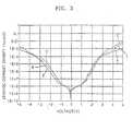
- FIG. 3is a graph illustrating a leakage current density with respect to a voltage applied to the capacitor according to an exemplary embodiment of the present invention.
- graphs T, B, and Crepresent leakage current densities of capacitors formed in an upper part, a lower part, and a middle part of a wafer respectively when the wafer having the capacitors depicted in FIG. 2, is vertically positioned.
- the capacitors formed on the upper, lower, and middle parts of the wafershow little differences in their leakage current densities, and the leakage current densities are lower than 10 -7 A/cm 2 within a driving voltage.
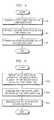
- the method of manufacturing the capacitorincludes first through third operations 60, 62, and 64.
- a first oxide filmis formed on a lower electrode.
- the lower electrodeis preferably a silicon electrode doped with a conductive dopant, but the lower electrode can also be another conductive electrode such as a titanium nitride electrode.
- the first oxide filmis used partly as a dielectric film of a capacitor, but mainly as a reaction barrier film that prevents an unwanted reaction between a second oxide film which will be formed later and the lower electrode. Therefore, it is desirable that the dielectric film is formed without a component that can react with a component, i.e., silicon, included in the lower electrode.
- the thickness of the first oxide filmis preferably formed to about 2 nm, which is thinner than the second oxide film, but may also thicker or thinner than 2 nm.
- the first oxide filmis formed to a thickness of a few nano meters, it is preferable that the first oxide film is formed using an ALD method in which thickness and composition can be controlled instead of a widely used thin film deposition method such as a conventional CVD method.
- the first oxide filmcan be formed with a single layer film, but can also be formed with a double layer film.
- the first oxide filmcan be formed of a hafnium oxide film and/or an aluminum oxide film.
- a second oxide filmis formed on the first oxide film.
- the second oxide filmperforms the same function as the second dielectric film 44. Therefore, it is preferable that the second oxide film is an oxide film including positive ions with larger radii than those in the first oxide film.
- the second oxide filmis formed of an oxide film that includes a lanthanide element such as a lanthanum oxide film (LaO).
- LaOlanthanum oxide film
- the second oxide filmis formed to a thickness of a few nano meters like the first oxide film.
- the second oxide filmis formed to the same thickness or thicker than the first oxide film. Since the second oxide film is also formed to a thickness of a few nano meters, it is preferably formed by an ALD method as opposed to a conventional thin film deposition method. The forming of the second oxide film using the ALD method will be described later.
- an upper electrodeis formed on the second oxide film.
- the upper electrodeis a titanium nitride electrode or can be a silicon electrode doped with a conductive dopant.
- the second operation 62can further be divide into three sub-operations 62a, 62b, and 62c.
- a detailed method of forming the second oxide film using an ALD methodis performed in the sub-operations 62a, 62b, and 62c.
- the second oxide filmis a lanthanum oxide film (La 2 O 3 ).
- a precursor that includes a metal component (La) of the second oxide filmsuch as (La(tmhd) 3 , La(N(Si(Me) 3 ) 2 ) 3 , or La(iPrCp) 3 , is deposited on the first oxide film. Then, the precursor layer is formed by performing a first exhaust process, and remaining precursors are removed form the reaction chamber.
- a metal component (La) of the second oxide filmsuch as (La(tmhd) 3 , La(N(Si(Me) 3 ) 2 ) 3 , or La(iPrCp) 3
- the precursor layeris oxidized. More specifically, an oxidation gas such as water vapor is supplied to the reaction chamber after the first exhaust process. Then, the second oxide film, i.e., the lanthanum oxide film is formed on the lower electrode through a substitution reaction between the oxidation gas and the precursor layer, that is, oxidation of the precursor layer. Then, an unreacted portion of the oxidation gas in the reaction chamber is removed by performing a second exhaust process.
- an oxidation gassuch as water vapor
- impuritiesare removed form the second oxide film. More specifically, excess water vapor included in the second oxide film is removed by supplying ozone to the reaction chamber after performing the second exhaust process. Then, a third exhaust process is performed to remove remaining ozone from the reaction chamber.
- the third sub-operation 62cis regarded as a drying process from the point of view that the water vapor included in the second oxide film is removed.
- the third sub-operation 62cis also regarded as a second oxidation process because the precursor layer can further be oxidized by the supplied ozone while removing impurities.
- Table 1illustrates whether a second oxide film is formed, whether water vapor remains in the second oxide film, and a leakage current density in the second oxide film according to the oxidation process used to form the second oxide film on the lower electrode using an ALD method.
- the second oxide filmis not formed on the lower electrode when ozone is used as the oxidation gas or when water vapor (H 2 O) is supplied to the reaction chamber after supplying the ozone.
- the second oxide filmis formed on the lower electrode.
- the water vapor (H 2 O)is included in the formed second oxide film and the leakage current density is as high as 10 -1 A/cm 2 .
- a semiconductor memory device including the capacitor depicted in FIG. 2 according to an exemplary embodiment of the present inventionwill now be described.
- the memory deviceincludes first and second doped regions 74 and 76 doped with a conductive dopant in a substrate 70.
- the first and second doped regions 74 and 76are separated by a predetermined distance.
- the first region 74is a source region and the second region 76 is a drain region.
- a channel regionis formed between the two regions 74 and 76 on the substrate 70, and a gate stack 72 is disposed on the channel region.
- the gate stack 72turns the channel region on or off according to a voltage applied to the gate stack 72.
- the gate stack 72includes a gate insulating film (not shown) and a gate conductive layer (not shown).
- the substrate 70, the first and second regions 74 and 76, and the gate stack 72constitute a MOSFET.
- a first inter-layer insulating layer 78 that covers the gate stack 72 and part of the substrate 70, and a first contact hole 80 that exposes the second region 76is formed in the first inter-layer insulating layer 78.
- the first contact hole 80is filled with a first conductive plug 82 such as polysilicon doped with a conductive dopant.
- a capacitor Cis formed on the first conductive plug 82 and the first inter-layer insulating layer 78 and covers the entire surface of the first conductive plug 82.
- the capacitor Cis preferably the same as the capacitor C depicted in FIG. 2. Therefore, descriptions of detailed structure and performances are omitted.
- the lower electrode 40 and the first conductive plug 82are preferably formed of the same conductive material but can also be formed of different conductive materials.
- a second inter-layer insulating layer 84is formed on the capacitor C and the first inter-layer insulating layer 78 and covers the capacitor C.
- a second contact hole 86 that exposes the first region 74is formed in the first inter-layer insulating layer 78 and the second inter-layer insulating layer 84.
- the second contact hole 86is filled with a second conductive plug 88.
- the second conductive plug 88is preferably formed of polysilicon doped with a conductive dopant, but can also be formed of a different conductive material.
- a conductive layer 90is formed on the second conduction plug 88 and the second inter-layer insulating layer 84 and covers an entire surface of the second conductive plug 88.
- the conductive layer 90is a bit line and cross to the gate stack 72.
- the conductive layer 90 and the second conductive plug 88are preferably formed of the same conductive material but can also be formed of different conductive materials.
- the capacitor according to the exemplary embodiment of the present inventionincludes a reaction barrier film that prevents an unwanted reaction between an oxide film which includes a lanthanide element and is used as a dielectric film, and a lower and/or an upper electrode that includes silicon. Accordingly, electrical degradation of the capacitor due to silicate formation as a result of a reaction between lanthanide in the oxide film and the silicon can be avoided.
- water vaporis completely removed by ozone after forming the oxide film. That is, the oxide film is completely dried.
- a memory device including the capacitor according to the present inventioncan store data for a long time without loss, thereby increasing the reliability of the memory device.
- the first dielectric filmcan also be a non-oxide film that can prevent a reaction between an oxide film and an upper and/or lower electrode that includes silicon.
- the upper and lower electrodescan be formed of a material that does not include silicon, and the dielectric film can be replaced by lanthanide oxide film.
Landscapes
- Engineering & Computer Science (AREA)
- Power Engineering (AREA)
- Chemical & Material Sciences (AREA)
- Inorganic Chemistry (AREA)
- Manufacturing & Machinery (AREA)
- Microelectronics & Electronic Packaging (AREA)
- Ceramic Engineering (AREA)
- Semiconductor Memories (AREA)
- Formation Of Insulating Films (AREA)
- Fixed Capacitors And Capacitor Manufacturing Machines (AREA)
- Semiconductor Integrated Circuits (AREA)
Abstract
Description
- The present invention relates to a semiconductor device and a method ofmanufacturing the same, and more particularly, to a capacitor, a method ofmanufacturing the same and a memory device including the capacitor.
- A lanthanum oxide (La2O3) can be used as a dielectric film in a capacitor ofa semiconductor device.
- When a lanthanum oxide film is deposited on a silicon layer, a silicate isformed in the capacitor as a result of a reaction between the lanthanum oxide filmand silicon of the silicon layer. The formation of silicate results in loweringcharacteristics of the capacitor.
- As the integration density of semiconductor devices increases, it is requiredto form capacitors having larger capacitance in a narrow region. The capacitanceof a capacitor is proportional to a surface area of an electrode. Therefore, thecapacitance of a capacitor can be increased by forming the electrode in threedimensions.
- It is desirable that a thickness and a composition of a dielectric film areuniform even if the electrode of the capacitor has a complicated structure.
- However, a conventional deposition method such as a chemical vapordeposition (CVD) method is not suitable for forming a dielectric film having auniform thickness and composition on an electrode with a complicated structuredue to process characteristics of the CVD method.
- An atomic layer deposition (ALD) method for forming a thin film on a lowerstructure of a complicated structure has been introduced, in which a thin film with adesired composition can be deposited in a deep region of a complicated structure.This method provides a uniformity of thickness and composition of a thin film tosome degree.
- Therefore, the ALD method can be used for forming a dielectric film havinga uniform thickness and composition on a capacitor electrode having acomplicated structure.
- The lanthanum oxide film can also be formed using the ALD method.However, there is a possibility of characteristic changes of the lanthanum oxidefilm resulting from absorption of water vapor (H2O) when the lanthanum oxide isexposed to the air because lanthanides are hygroscopic.
- That is, when forming the lanthanum oxide film using the ALD method afterdeposition of a lanthanum precursor layer, a large amount of water vapor can beabsorbed by the lanthanum precursor layer during an oxidization process usingwater vapor (H2O). In this case, electrical characteristics such as an ability of thelanthanum oxide film to prevent a leakage current can be degraded.
- FIG. 1 is a graph illustrating the increase in the leakage current densitywhen water vapor is used as an oxidation gas for forming a few oxide films suchas the lanthanum oxide film using the ALD method. Reference character B1represents a leakage current density of an aluminum oxide film formed to athickness of 40 Å, and B2 represents that of a hafnium oxide film formed in athickness of 45 Å. Reference character B3, B4, and B5 represent leakagecurrents of precursors La(tmhd)3, La(N(Si(Me)3)2)3, and La(iPrCp)3, respectively.
- According to an aspect of the present invention, there is provided acapacitor of a semiconductor device, comprising a lower electrode, a dielectric film,and an upper electrode with a first reaction barrier film formed between the lowerelectrode and the dielectric film.
- The dielectric film is an oxide film that includes a lanthanide element.
- A second reaction barrier film can further be formed between the upperelectrode and the dielectric film.
- The first and second reaction barrier films are each a hafnium oxide film oran aluminum oxide film that includes positive ions with smaller radii than positiveions of the lanthanum oxide film (La2O3).
- According to another aspect of the present invention, there is provided amethod of forming a capacitor comprising forming a lower electrode, forming a firstreaction barrier film on the lower electrode, forming a precursor layer that includesa metal element on the first reaction barrier film, forming an oxide film that includes a metal element by oxidizing the metal element of the precursor layer, drying theoxide film, and forming an upper electrode on the dried oxide film.
- The lower electrode is a silicon electrode doped with a conductive dopant,and the upper electrode is a titanium nitride film.
- A second reaction barrier film can further be formed between the dried oxidefilm and the upper electrode, and the lower electrode and the upper electrode canbe silicon electrodes doped with a conductive dopant or titanium nitride films.
- An exhaust process may be performed after forming the precursor layer,after forming the oxide film, and after drying the oxide film.
- The forming the oxide film may comprise flowing water vapor over theprecursor layer to firstly oxidize the precusor layer.
- The forming the oxide film may further comprises supplying ozone over thefirstly oxidized precursor layer to secondly oxidize the firstly oxidized precursorlayer.
- The firstly and secondly oxidation processes may be repeated.
- The oxide film is dried by flowing ozone over the oxide film.
- The first and second reaction barrier films can each be a hafnium oxide filmor an aluminum oxide film that includes positive ions with smaller radii thanpositive ions of the dielectric film.
- According to yet another aspect of the present invention, there is provided asemiconductor memory device having a capacitor connected to a transistor,wherein the capacitor includes a lower electrode, a dielectric film, an upperelectrode and a first reaction barrier film interposed between the lower electrodeand the dielectric film.
- Since, the capacitor according to the present invention prevents anunwanted reaction between the lanthanum oxide film used as the dielectric filmand the lower electrode, and prevents inclusion of a large amount of vapor in thelanthanum oxide while forming the oxide film, degradation of electricalcharacteristics of the lanthanum oxide, that is, the capacitor, are prevented,thereby increasing the reliability of the semiconductor memory device that includesthe capacitor.
- The present invention provides a capacitor that inhibits an unwantedreaction between a dielectric film and a lower electrode on which the dielectric filmis formed, and prevents a degradation of electrical characteristics of a dielectricfilm formed by atomic layer deposition (ALD) by preventing the dielectric film fromabsorbing a large amount of water vapor.
- The present invention also provides a method of manufacturing thecapacitor.
- The present invention also provides a semiconductor memory deviceincluding the capacitor.
- The above and other features and advantages of the present invention willbecome more apparent by describing in detail exemplary embodiments thereofwith reference to the attached drawings in which:
- FIG. 1 is a graph illustrating leakage current density with respect tothickness of a dielectric film of a conventional capacitor for several types ofdielectric film;
- FIG. 2 is a cross-sectional view of a capacitor according to an exemplaryembodiment of the present invention;
- FIG. 3 is a graph illustrating a leakage current density of the capacitordepicted in FIG. 2 with respect to a voltage applied to the capacitor;
- FIG. 4 is a block diagram for describing each operation of manufacturing acapacitor depicted in FIG. 2;
- FIG. 5 is a block diagram for describing a second operation ofmanufacturing a capacitor depicted in FIG. 4; and
- FIG. 6 is a cross-sectional view of a semiconductor device having thecapacitor depicted in FIG. 2.
- The present invention will now be described more fully with reference to theaccompanying drawings in which exemplary embodiments of the present inventionare shown. However, this invention may be embodied in many different formsand should not be construed as being limited to the embodiments set forth herein.Rather, these embodiments are provided so that this disclosure will be thorough and complete and fully convey the concept of the invention to those skilled in theart. In the drawings, the thicknesses of layers and regions are exaggerated forclarity.
- A capacitor according to an exemplary embodiment of the present inventionwill now be described.
- FIG. 2 is a cross-sectional view of a capacitor according to an exemplaryembodiment of the present invention.
- Referring to FIG. 2, the capacitor includes a
lower electrode 40, a dielectricfilm DL, and anupper electrode 46. Thelower electrode 40 is a silicon electrodedoped with a conductive dopant and can be formed of titanium nitride (TiN). Thedielectric film DL includes a firstdielectric film 42 and a seconddielectric film 44.The firstdielectric film 42 prevents an unwanted reaction between thelowerelectrode 40 and the seconddielectric film 44, that is, it prevents silicate formation.The firstdielectric film 42 is preferably formed of a dielectric film including positiveions with smaller radii than those in the seconddielectric film 44, such as ahafnium oxide film (HfO2) or an aluminum oxide film (Al2O3). The thickness of thefirstdielectric film 42 can be about 2 nm, but is preferably thinner than the seconddielectric film 44. The seconddielectric film 44 is preferably formed of an oxidefilm that includes a lanthanide element, such as lanthanum oxide (LaO). Thethickness of the seconddielectric film 44 is preferably 2 to 10 nm, but may thickeror thinner than this. Theupper electrode 46 is preferably a titanium nitride (TiN)electrode, but can also be a silicon electrode doped with a conductive dopant.However, in the latter case, a reaction barrier film that prevents a silicate reactionbetween theupper electrode 46 and the seconddielectric film 44 can further beformed therebetween. Theupper electrode 46 and thelower electrode 40 can beformed of the same material. - FIG. 3 is a graph illustrating a leakage current density with respect to avoltage applied to the capacitor according to an exemplary embodiment of thepresent invention. In FIG. 3, graphs T, B, and C represent leakage currentdensities of capacitors formed in an upper part, a lower part, and a middle part of awafer respectively when the wafer having the capacitors depicted in FIG. 2, isvertically positioned.
- Referring to the graphs T, B, and C, the capacitors formed on the upper,lower, and middle parts of the wafer show little differences in their leakage currentdensities, and the leakage current densities are lower than 10-7A/cm2 within adriving voltage.
- From the graphs T, B, and C, it also is seen that the leakage currentcharacteristics of the capacitors formed on all regions of the wafer are alsosuperior as in the leakage current characteristics of the capacitors formed on theupper, lower, and middle parts of the wafer.
- A method of manufacturing the capacitor depicted in FIG. 2 according to anexemplary embodiment of the present invention will now be described.
- Referring to FIG. 4, the method of manufacturing the capacitor includes firstthrough
third operations - In the
first operation 60, a first oxide film is formed on a lower electrode.The lower electrode is preferably a silicon electrode doped with a conductivedopant, but the lower electrode can also be another conductive electrode such asa titanium nitride electrode. The first oxide film is used partly as a dielectric filmof a capacitor, but mainly as a reaction barrier film that prevents an unwantedreaction between a second oxide film which will be formed later and the lowerelectrode. Therefore, it is desirable that the dielectric film is formed without acomponent that can react with a component, i.e., silicon, included in the lowerelectrode. The thickness of the first oxide film is preferably formed to about 2 nm,which is thinner than the second oxide film, but may also thicker or thinner than 2nm. Since the first oxide film is formed to a thickness of a few nano meters, it ispreferable that the first oxide film is formed using an ALD method in whichthickness and composition can be controlled instead of a widely used thin filmdeposition method such as a conventional CVD method. The first oxide film canbe formed with a single layer film, but can also be formed with a double layer film.The first oxide film can be formed of a hafnium oxide film and/or an aluminumoxide film. - In the second operation, a second oxide film is formed on the first oxide film.The second oxide film performs the same function as the
second dielectric film 44.Therefore, it is preferable that the second oxide film is an oxide film including positive ions with larger radii than those in the first oxide film. It is desirable thatthe second oxide film is formed of an oxide film that includes a lanthanide elementsuch as a lanthanum oxide film (LaO). Preferably, the second oxide film isformed to a thickness of a few nano meters like the first oxide film. However, thesecond oxide film is formed to the same thickness or thicker than the first oxidefilm. Since the second oxide film is also formed to a thickness of a few nanometers, it is preferably formed by an ALD method as opposed to a conventionalthin film deposition method. The forming of the second oxide film using the ALDmethod will be described later. - In the
third operation 64, an upper electrode is formed on the second oxidefilm. The upper electrode is a titanium nitride electrode or can be a siliconelectrode doped with a conductive dopant. - Referring to FIG. 5, the
second operation 62 can further be divide into threesub-operations - More specifically, in the
first sub-operation 62a, a precursor that includes ametal component (La) of the second oxide film, such as (La(tmhd)3,La(N(Si(Me)3)2)3, or La(iPrCp)3, is deposited on the first oxide film. Then, theprecursor layer is formed by performing a first exhaust process, and remainingprecursors are removed form the reaction chamber. - In the
second sub-operation 62b, the precursor layer is oxidized. Morespecifically, an oxidation gas such as water vapor is supplied to the reactionchamber after the first exhaust process. Then, the second oxide film, i.e., thelanthanum oxide film is formed on the lower electrode through a substitutionreaction between the oxidation gas and the precursor layer, that is, oxidation of theprecursor layer. Then, an unreacted portion of the oxidation gas in the reactionchamber is removed by performing a second exhaust process. - In the
third sub-operation 62c, impurities are removed form the secondoxide film. More specifically, excess water vapor included in the second oxidefilm is removed by supplying ozone to the reaction chamber after performing the second exhaust process. Then, a third exhaust process is performed to removeremaining ozone from the reaction chamber. - The
third sub-operation 62c is regarded as a drying process from the pointof view that the water vapor included in the second oxide film is removed. - The
third sub-operation 62c is also regarded as a second oxidation processbecause the precursor layer can further be oxidized by the supplied ozone whileremoving impurities. - Table 1 illustrates whether a second oxide film is formed, whether watervapor remains in the second oxide film, and a leakage current density in thesecond oxide film according to the oxidation process used to form the secondoxide film on the lower electrode using an ALD method.
Oxidation Process O3 H20 H 20-->O3O3--> H 20Film formation no yes yes no water vapor (H2O) inclusion - yes no - leakage current density (A/cm2) - 10-1 10-7 - Referring to Table 1, the second oxide film is not formed on the lowerelectrode when ozone is used as the oxidation gas or when water vapor (H2O) issupplied to the reaction chamber after supplying the ozone.
- When the water vapor (H2O) is used as the oxidation gas, the second oxidefilm is formed on the lower electrode. However, the water vapor (H2O) is includedin the formed second oxide film and the leakage current density is as high as 10-1A/cm2.
- On the other hand, when ozone is supplied to the chamber after supplyingthe water vapor (H2O) according to the method of manufacturing the capacitoraccording to the present invention, not only is the second oxide film formed on thelower electrode, but the water vapor (H2O) does not remain in the formed secondoxide film and the leakage current density is as low as 10-7 A/cm2.
- A semiconductor memory device including the capacitor depicted in FIG. 2according to an exemplary embodiment of the present invention will now bedescribed.
- Referring to FIG. 6, the memory device includes first and second
dopedregions substrate 70. The firstand seconddoped regions first region 74 is a source region and thesecond region 76 is a drain region.A channel region is formed between the tworegions substrate 70,and agate stack 72 is disposed on the channel region. Thegate stack 72 turnsthe channel region on or off according to a voltage applied to thegate stack 72.Thegate stack 72 includes a gate insulating film (not shown) and a gateconductive layer (not shown). Thesubstrate 70, the first andsecond regions gate stack 72 constitute a MOSFET. A firstinter-layer insulatinglayer 78 that covers thegate stack 72 and part of thesubstrate 70, and afirstcontact hole 80 that exposes thesecond region 76 is formed in the firstinter-layerinsulating layer 78. Thefirst contact hole 80 is filled with a firstconductive plug 82 such as polysilicon doped with a conductive dopant. A capacitor C is formedon the firstconductive plug 82 and the firstinter-layer insulating layer 78 andcovers the entire surface of the firstconductive plug 82. The capacitor C ispreferably the same as the capacitor C depicted in FIG. 2. Therefore,descriptions of detailed structure and performances are omitted. Thelowerelectrode 40 and the firstconductive plug 82 are preferably formed of the sameconductive material but can also be formed of different conductive materials. Asecondinter-layer insulating layer 84 is formed on the capacitor C and the firstinter-layer insulating layer 78 and covers the capacitor C. Asecond contact hole 86 that exposes thefirst region 74 is formed in the firstinter-layer insulating layer 78 and the secondinter-layer insulating layer 84. Thesecond contact hole 86 isfilled with a secondconductive plug 88. The secondconductive plug 88 ispreferably formed of polysilicon doped with a conductive dopant, but can also beformed of a different conductive material. Aconductive layer 90 is formed on thesecond conduction plug 88 and the secondinter-layer insulating layer 84 andcovers an entire surface of the secondconductive plug 88. Theconductive layer 90 is a bit line and cross to thegate stack 72. Theconductive layer 90 and thesecondconductive plug 88 are preferably formed of the same conductive materialbut can also be formed of different conductive materials. - Since the memory device described heretofore is equipped with thecapacitor C depicted in FIG. 2, data stored in the capacitor C can be maintainedfor a long time in a normal state, thereby increasing reliability of the memorydevice.
- The capacitor according to the exemplary embodiment of the presentinvention includes a reaction barrier film that prevents an unwanted reactionbetween an oxide film which includes a lanthanide element and is used as adielectric film, and a lower and/or an upper electrode that includes silicon.Accordingly, electrical degradation of the capacitor due to silicate formation as aresult of a reaction between lanthanide in the oxide film and the silicon can beavoided. In the process of forming the oxide film using an ALD method, watervapor is completely removed by ozone after forming the oxide film. That is, theoxide film is completely dried. Thus, electrical degradation of the capacitor due toan inclusion of water vapor in the oxide film is prevented. A memory deviceincluding the capacitor according to the present invention can store data for a longtime without loss, thereby increasing the reliability of the memory device.
- In the capacitor according to the present invention, the first dielectric filmcan also be a non-oxide film that can prevent a reaction between an oxide film andan upper and/or lower electrode that includes silicon. Also, the upper and lowerelectrodes can be formed of a material that does not include silicon, and thedielectric film can be replaced by lanthanide oxide film.
- While the present invention has been particularly shown and described withreference to exemplary embodiments thereof, it will be understood by those ofordinary skill in the art that various changes in form and details may be madetherein without departing from the scope of the present invention as defined by thefollowing claims.
Claims (24)
- A capacitor of a semiconductor device comprising:a lower electrode;a dielectric film on the lower electrode;an upper electrode on the dielectric film; anda first reaction barrier film that prevents a reaction between the lowerelectrode and the dielectric film, interposed between the lower electrode and thedielectric film.
- The capacitor of claim 1, wherein the lower electrode is a siliconelectrode doped with a conductive dopant.
- The capacitor of claim 1 or 2, wherein the first reaction barrier film is oneof a hafnium oxide film and an aluminum oxide film that includes positive ions withsmaller radii than positive ions of the dielectric film.
- The capacitor of any preceding claim, wherein the dielectric film is anoxide film that includes a lanthanide element.
- The capacitor of claim 4, wherein the oxide film that includes thelanthanide element is La2O3 film.
- The capacitor of any preceding claim, wherein the upper electrode is atitanium nitride film.
- The capacitor of any preceding claim, further comprising a secondreaction barrier film between the upper electrode and the dielectric film whereinthe upper electrode is a silicon electrode doped with a conductive dopant.
- The capacitor of claim 7, wherein the second reaction barrier film is oneof a hafnium oxide film and an aluminum oxide film that includes positive ions withsmaller radii than positive ions of the dielectric film.
- A method of forming a capacitor comprising:forming a lower electrode;forming a first reaction barrier film on the lower electrode;forming a precursor layer that includes a metal element on the first reactionbarrier film;forming an oxide film that includes the metal element by oxidizing theprecursor layer;drying the oxide film; andforming an upper electrode on the dried oxide film.
- The method of claim 9 further comprising, before forming the upperelectrode, forming a second reaction barrier film on the dried oxide film.
- The method of claim 10, wherein the lower electrode and the upperelectrode are each one of a silicon electrode doped with a conductive dopant anda titanium nitride film.
- The method of claim 10, wherein the second reaction barrier film is oneof a hafnium oxide film and an aluminum oxide film that includes positive ions withsmaller radii than positive ions of the dielectric film.
- The method of claim 9, 10, 11 or 12 wherein the lower electrode isformed of a silicon electrode doped with a conductive dopant, and the upperelectrode is formed of a titanium nitride film.
- The method of any of claims 9 to 13, wherein the lower and upperelectrodes are a titanium nitride film.
- The method of any of claims 9 to 14, wherein an exhaust process isperformed after forming the precursor layer.
- The method of any of claims 9 to 14, wherein an exhaust process isperformed after forming the oxide film.
- The method of any of claims 9 to 14, wherein an exhaust process isperformed after drying the oxide film.
- The method of any of claims 9 to 14, wherein the forming the oxide filmcomprises flowing water vapor over the precursor layer to firstly oxidize theprecusor layer.
- The method of claim 18, wherein the forming the oxide film furthercomprises supplying ozone over the firstly oxidized precursor layer to secondlyoxidize the firstly oxidized precursor layer.
- The method of claim 19, wherein, in forming the oxide film, the firstlyand secondly oxidations are repeated.
- The method of any of claims 9 to 20, wherein the metal element is alanthanide element.
- The method of any of claims 9 to 21, wherein drying the oxide filmcomprises flowing ozone over the oxide film.
- The method of any of claims 9 to 22, wherein the first reaction barrierfilm is one of a hafnium oxide film and an aluminum oxide film that includespositive ions with smaller radii than positive ions of the dielectric film.
- A semiconductor memory device including a capacitor connected to atransistor, wherein the capacitor is a capacitor according to any of claims 1 to 8.
Applications Claiming Priority (2)
| Application Number | Priority Date | Filing Date | Title |
|---|---|---|---|
| KR2003056857 | 2003-08-18 | ||
| KR1020030056857AKR101001741B1 (en) | 2003-08-18 | 2003-08-18 | A capacitor of a semiconductor device, a method of manufacturing the same, and a memory device having a capacitor |
Publications (2)
| Publication Number | Publication Date |
|---|---|
| EP1508906A2true EP1508906A2 (en) | 2005-02-23 |
| EP1508906A3 EP1508906A3 (en) | 2006-12-06 |
Family
ID=34056926
Family Applications (1)
| Application Number | Title | Priority Date | Filing Date |
|---|---|---|---|
| EP04254930AWithdrawnEP1508906A3 (en) | 2003-08-18 | 2004-08-17 | Capacitor, method of manufacturing the same and memory device including the same |
Country Status (5)
| Country | Link |
|---|---|
| US (2) | US20050082593A1 (en) |
| EP (1) | EP1508906A3 (en) |
| JP (1) | JP2005064523A (en) |
| KR (1) | KR101001741B1 (en) |
| CN (1) | CN1610120A (en) |
Cited By (7)
| Publication number | Priority date | Publication date | Assignee | Title |
|---|---|---|---|---|
| US7053432B2 (en)* | 2000-08-31 | 2006-05-30 | Micron Technology, Inc. | Enhanced surface area capacitor fabrication methods |
| US7105065B2 (en) | 2002-04-25 | 2006-09-12 | Micron Technology, Inc. | Metal layer forming methods and capacitor electrode forming methods |
| US7109542B2 (en) | 2000-08-31 | 2006-09-19 | Micron Technology, Inc. | Capacitor constructions having a conductive layer |
| US7112503B1 (en) | 2000-08-31 | 2006-09-26 | Micron Technology, Inc. | Enhanced surface area capacitor fabrication methods |
| US7440255B2 (en) | 2003-07-21 | 2008-10-21 | Micron Technology, Inc. | Capacitor constructions and methods of forming |
| US7662693B2 (en) | 2007-09-26 | 2010-02-16 | Micron Technology, Inc. | Lanthanide dielectric with controlled interfaces |
| DE102007047857B4 (en)* | 2006-11-29 | 2012-09-13 | Qimonda Ag | Semiconductor devices and methods of making same |
Families Citing this family (10)
| Publication number | Priority date | Publication date | Assignee | Title |
|---|---|---|---|---|
| KR100590592B1 (en)* | 2004-08-20 | 2006-06-19 | 삼성전자주식회사 | Capacitor including dielectric layer with reduced leakage current and method of manufacturing same |
| KR100693890B1 (en)* | 2005-04-21 | 2007-03-12 | 삼성전자주식회사 | Manufacturing Method of Semiconductor Device Having Reaction Barrier Film |
| JP2007266474A (en)* | 2006-03-29 | 2007-10-11 | Hitachi Ltd | Semiconductor memory device |
| JP2008166360A (en)* | 2006-12-27 | 2008-07-17 | Hitachi Ltd | Semiconductor integrated circuit device |
| WO2010144092A1 (en) | 2009-06-12 | 2010-12-16 | Hewlett-Packard Development Company, L.P. | Capacitive crossbar arrays |
| US8750024B2 (en) | 2009-06-18 | 2014-06-10 | Hewlett-Packard Development Company, L.P. | Memcapacitor |
| US20110298089A1 (en)* | 2010-06-03 | 2011-12-08 | International Business Machines Corporation | Trench capacitor and method of fabrication |
| KR101977271B1 (en)* | 2013-04-05 | 2019-05-10 | 에스케이하이닉스 주식회사 | Method for fabricating semiconductor device |
| KR102434565B1 (en)* | 2018-01-19 | 2022-08-19 | 미쓰비시덴키 가부시키가이샤 | Thin-Layer Capacitors and Methods for Manufacturing Thin-Layer Capacitors |
| KR102665567B1 (en) | 2018-04-12 | 2024-05-14 | 엘에스엠트론 주식회사 | Agricultural working machine with trailing load control device |
Citations (1)
| Publication number | Priority date | Publication date | Assignee | Title |
|---|---|---|---|---|
| WO2002031875A2 (en) | 2000-10-10 | 2002-04-18 | Asm America, Inc. | Dielectric interface films and methods therefor |
Family Cites Families (17)
| Publication number | Priority date | Publication date | Assignee | Title |
|---|---|---|---|---|
| JP3351856B2 (en)* | 1992-04-20 | 2002-12-03 | テキサス インスツルメンツ インコーポレイテツド | Method of manufacturing structure and capacitor |
| US6194751B1 (en)* | 1994-11-15 | 2001-02-27 | Radiant Technologies, Inc | Ferroelectric based memory devices utilizing low Curie point ferroelectrics and encapsulation |
| JPH0969509A (en)* | 1995-09-01 | 1997-03-11 | Matsushita Electron Corp | Cleaning/etching/drying system for semiconductor wafer and using method thereof |
| US6218260B1 (en)* | 1997-04-22 | 2001-04-17 | Samsung Electronics Co., Ltd. | Methods of forming integrated circuit capacitors having improved electrode and dielectric layer characteristics and capacitors formed thereby |
| US5841186A (en)* | 1997-08-19 | 1998-11-24 | United Microelectronics Corp. | Composite dielectric films |
| KR100293713B1 (en)* | 1998-12-22 | 2001-07-12 | 박종섭 | Method of manufacturing capacitor of memory element |
| US6576053B1 (en)* | 1999-10-06 | 2003-06-10 | Samsung Electronics Co., Ltd. | Method of forming thin film using atomic layer deposition method |
| US6607950B2 (en)* | 2000-03-30 | 2003-08-19 | Interuniversitair Microelektronic Centrum (Imec) | MIS transistors with a metal gate and high-k dielectric and method of forming |
| US6503314B1 (en)* | 2000-08-28 | 2003-01-07 | Sharp Laboratories Of America, Inc. | MOCVD ferroelectric and dielectric thin films depositions using mixed solvents |
| US6794694B2 (en)* | 2000-12-21 | 2004-09-21 | Agere Systems Inc. | Inter-wiring-layer capacitors |
| US6511873B2 (en)* | 2001-06-15 | 2003-01-28 | International Business Machines Corporation | High-dielectric constant insulators for FEOL capacitors |
| US6642131B2 (en)* | 2001-06-21 | 2003-11-04 | Matsushita Electric Industrial Co., Ltd. | Method of forming a silicon-containing metal-oxide gate dielectric by depositing a high dielectric constant film on a silicon substrate and diffusing silicon from the substrate into the high dielectric constant film |
| US6734477B2 (en)* | 2001-08-08 | 2004-05-11 | Agilent Technologies, Inc. | Fabricating an embedded ferroelectric memory cell |
| US7087481B2 (en)* | 2002-08-28 | 2006-08-08 | Micron Technology, Inc. | Systems and methods for forming metal oxides using metal compounds containing aminosilane ligands |
| US6858524B2 (en)* | 2002-12-03 | 2005-02-22 | Asm International, Nv | Method of depositing barrier layer for metal gates |
| KR100546324B1 (en)* | 2003-04-22 | 2006-01-26 | 삼성전자주식회사 | Metal oxide thin film formation method by ALD, lanthanum oxide film formation method and high-k dielectric film formation method of semiconductor device |
| KR20050007496A (en)* | 2003-07-08 | 2005-01-19 | 삼성전자주식회사 | Method for forming multi-layer using atomic layer deposition and method for forming capacitor of semiconductor device |
- 2003
- 2003-08-18KRKR1020030056857Apatent/KR101001741B1/ennot_activeExpired - Fee Related
- 2004
- 2004-08-17EPEP04254930Apatent/EP1508906A3/ennot_activeWithdrawn
- 2004-08-17JPJP2004237223Apatent/JP2005064523A/ennot_activeWithdrawn
- 2004-08-18USUS10/920,455patent/US20050082593A1/ennot_activeAbandoned
- 2004-08-18CNCNA2004100959626Apatent/CN1610120A/enactivePending
- 2008
- 2008-12-10USUS12/314,427patent/US20090126173A1/ennot_activeAbandoned
Patent Citations (1)
| Publication number | Priority date | Publication date | Assignee | Title |
|---|---|---|---|---|
| WO2002031875A2 (en) | 2000-10-10 | 2002-04-18 | Asm America, Inc. | Dielectric interface films and methods therefor |
Non-Patent Citations (1)
| Title |
|---|
| YAMADA ET AL.: "MOCVD of High-Dielectric-Constant Lanthanum Oxide Thin Films", JOURNAL ELECTROCHEMICAL SOCIETY, vol. 150, no. 8, 2003, pages G429 - G435 |
Cited By (11)
| Publication number | Priority date | Publication date | Assignee | Title |
|---|---|---|---|---|
| US7053432B2 (en)* | 2000-08-31 | 2006-05-30 | Micron Technology, Inc. | Enhanced surface area capacitor fabrication methods |
| US7109542B2 (en) | 2000-08-31 | 2006-09-19 | Micron Technology, Inc. | Capacitor constructions having a conductive layer |
| US7112503B1 (en) | 2000-08-31 | 2006-09-26 | Micron Technology, Inc. | Enhanced surface area capacitor fabrication methods |
| US7288808B2 (en) | 2000-08-31 | 2007-10-30 | Micron Technology, Inc. | Capacitor constructions with enhanced surface area |
| US7105065B2 (en) | 2002-04-25 | 2006-09-12 | Micron Technology, Inc. | Metal layer forming methods and capacitor electrode forming methods |
| US7440255B2 (en) | 2003-07-21 | 2008-10-21 | Micron Technology, Inc. | Capacitor constructions and methods of forming |
| DE102007047857B4 (en)* | 2006-11-29 | 2012-09-13 | Qimonda Ag | Semiconductor devices and methods of making same |
| US7662693B2 (en) | 2007-09-26 | 2010-02-16 | Micron Technology, Inc. | Lanthanide dielectric with controlled interfaces |
| US7956426B2 (en) | 2007-09-26 | 2011-06-07 | Micron Technology, Inc. | Lanthanide dielectric with controlled interfaces |
| US8153497B2 (en) | 2007-09-26 | 2012-04-10 | Micron Technology, Inc. | Lanthanide dielectric with controlled interfaces |
| US8399332B2 (en) | 2007-09-26 | 2013-03-19 | Micron Technology, Inc. | Lanthanide dielectric with controlled interfaces |
Also Published As
| Publication number | Publication date |
|---|---|
| US20090126173A1 (en) | 2009-05-21 |
| US20050082593A1 (en) | 2005-04-21 |
| EP1508906A3 (en) | 2006-12-06 |
| JP2005064523A (en) | 2005-03-10 |
| CN1610120A (en) | 2005-04-27 |
| KR20050019218A (en) | 2005-03-03 |
| KR101001741B1 (en) | 2010-12-15 |
Similar Documents
| Publication | Publication Date | Title |
|---|---|---|
| US20090126173A1 (en) | Method of manufacturing a capacitor and memory device including the same | |
| US6787413B2 (en) | Capacitor structure forming methods | |
| KR100636856B1 (en) | WLSI MOOS with high dielectric constant gate insulating film | |
| US7323422B2 (en) | Dielectric layers and methods of forming the same | |
| US8026184B2 (en) | Semiconductor device and method of manufacturing the same | |
| US7495264B2 (en) | Semiconductor device with high dielectric constant insulating film and manufacturing method for the same | |
| JP2002534818A (en) | Semiconductor structural element and method of manufacturing the same | |
| JPH0685173A (en) | Capacitors for semiconductor integrated circuits | |
| KR20040060443A (en) | Capacitor of a semiconductor device and manufacturing method whereof | |
| US20040072401A1 (en) | Method for forming capacitor | |
| CN1741271A (en) | Semiconductor integrated circuit device with mixed dielectric layer and method of manufacturing the same | |
| US6855594B1 (en) | Methods of forming capacitors | |
| JP3822378B2 (en) | Manufacturing method of semiconductor device | |
| US20060292810A1 (en) | Method of manufacturing a capacitor | |
| KR100641060B1 (en) | Method for manufacturing gate structure and method for manufacturing semiconductor device using same | |
| KR20060072338A (en) | Dielectric film formation method and capacitor formation method of semiconductor device using same | |
| US7371670B2 (en) | Method for forming a (TaO)1-x(TiO)xN dielectric layer in a semiconductor device | |
| KR100826978B1 (en) | Method for forming capacitor of semiconductor device | |
| KR20060136191A (en) | Method of manufacturing a capacitor | |
| JP4357146B2 (en) | Method for forming oxide dielectric film and method for manufacturing semiconductor device | |
| KR100546151B1 (en) | Capacitor Manufacturing Method of Semiconductor Device | |
| KR100790567B1 (en) | Semiconductor device having a high dielectric constant composite gate insulating film and its manufacturing method | |
| KR100376987B1 (en) | Fabricating method for capacitor of semiconductor device | |
| KR100268941B1 (en) | method for fabricating capacitor of semiconductor device | |
| JP2000323678A (en) | Method for manufacturing semiconductor device |
Legal Events
| Date | Code | Title | Description |
|---|---|---|---|
| PUAI | Public reference made under article 153(3) epc to a published international application that has entered the european phase | Free format text:ORIGINAL CODE: 0009012 | |
| AK | Designated contracting states | Kind code of ref document:A2 Designated state(s):AT BE BG CH CY CZ DE DK EE ES FI FR GB GR HU IE IT LI LU MC NL PL PT RO SE SI SK TR | |
| AX | Request for extension of the european patent | Extension state:AL HR LT LV MK | |
| PUAL | Search report despatched | Free format text:ORIGINAL CODE: 0009013 | |
| AK | Designated contracting states | Kind code of ref document:A3 Designated state(s):AT BE BG CH CY CZ DE DK EE ES FI FR GB GR HU IE IT LI LU MC NL PL PT RO SE SI SK TR | |
| AX | Request for extension of the european patent | Extension state:AL HR LT LV MK | |
| RIC1 | Information provided on ipc code assigned before grant | Ipc:H01G 4/12 20060101ALI20061027BHEP Ipc:H01L 21/02 20060101ALI20061027BHEP Ipc:H01G 4/10 20060101AFI20041222BHEP | |
| 17P | Request for examination filed | Effective date:20070321 | |
| AKX | Designation fees paid | Designated state(s):DE FR GB | |
| 17Q | First examination report despatched | Effective date:20080730 | |
| STAA | Information on the status of an ep patent application or granted ep patent | Free format text:STATUS: THE APPLICATION IS DEEMED TO BE WITHDRAWN | |
| 18D | Application deemed to be withdrawn | Effective date:20100302 |