EP1503411A1 - Conductive lines embedded in isolation regions - Google Patents
Conductive lines embedded in isolation regionsDownload PDFInfo
- Publication number
- EP1503411A1 EP1503411A1EP04103661AEP04103661AEP1503411A1EP 1503411 A1EP1503411 A1EP 1503411A1EP 04103661 AEP04103661 AEP 04103661AEP 04103661 AEP04103661 AEP 04103661AEP 1503411 A1EP1503411 A1EP 1503411A1
- Authority
- EP
- European Patent Office
- Prior art keywords
- active
- substrate
- zone
- integrated circuit
- isolation
- Prior art date
- Legal status (The legal status is an assumption and is not a legal conclusion. Google has not performed a legal analysis and makes no representation as to the accuracy of the status listed.)
- Withdrawn
Links
- 238000002955isolationMethods0.000titledescription69
- 239000000758substrateSubstances0.000claimsabstractdescription52
- 238000009413insulationMethods0.000claimsabstractdescription19
- 239000012212insulatorSubstances0.000claimsabstractdescription14
- 239000004065semiconductorSubstances0.000claimsabstractdescription8
- 239000010410layerSubstances0.000claimsdescription98
- 230000015654memoryEffects0.000claimsdescription39
- 238000000034methodMethods0.000claimsdescription20
- 238000009826distributionMethods0.000claimsdescription17
- VYPSYNLAJGMNEJ-UHFFFAOYSA-NSilicium dioxideChemical compoundO=[Si]=OVYPSYNLAJGMNEJ-UHFFFAOYSA-N0.000claimsdescription15
- 229910052814silicon oxideInorganic materials0.000claimsdescription15
- 239000004020conductorSubstances0.000claimsdescription12
- 239000000463materialSubstances0.000claimsdescription11
- 239000011241protective layerSubstances0.000claimsdescription5
- 230000001681protective effectEffects0.000claimsdescription4
- 229910052581Si3N4Inorganic materials0.000claimsdescription3
- 238000004519manufacturing processMethods0.000claimsdescription3
- 229910052751metalInorganic materials0.000claimsdescription3
- 239000002184metalSubstances0.000claimsdescription3
- HQVNEWCFYHHQES-UHFFFAOYSA-Nsilicon nitrideChemical compoundN12[Si]34N5[Si]62N3[Si]51N64HQVNEWCFYHHQES-UHFFFAOYSA-N0.000claimsdescription3
- 229910021421monocrystalline siliconInorganic materials0.000claimsdescription2
- 230000010287polarizationEffects0.000claimsdescription2
- 239000011248coating agentSubstances0.000claims1
- 238000000576coating methodMethods0.000claims1
- XUIMIQQOPSSXEZ-UHFFFAOYSA-NSiliconChemical group[Si]XUIMIQQOPSSXEZ-UHFFFAOYSA-N0.000description14
- 229910052710siliconInorganic materials0.000description14
- 239000010703siliconSubstances0.000description14
- 238000005530etchingMethods0.000description10
- 229910052732germaniumInorganic materials0.000description8
- GNPVGFCGXDBREM-UHFFFAOYSA-Ngermanium atomChemical compound[Ge]GNPVGFCGXDBREM-UHFFFAOYSA-N0.000description8
- 150000004767nitridesChemical class0.000description7
- 125000006850spacer groupChemical group0.000description5
- 230000015572biosynthetic processEffects0.000description3
- 230000010354integrationEffects0.000description3
- 229910021420polycrystalline siliconInorganic materials0.000description3
- 238000012549trainingMethods0.000description3
- NRTOMJZYCJJWKI-UHFFFAOYSA-NTitanium nitrideChemical compound[Ti]#NNRTOMJZYCJJWKI-UHFFFAOYSA-N0.000description2
- 230000007423decreaseEffects0.000description2
- 230000001627detrimental effectEffects0.000description2
- 238000010586diagramMethods0.000description2
- 238000005498polishingMethods0.000description2
- 239000011347resinSubstances0.000description2
- 229920005989resinPolymers0.000description2
- 239000000126substanceSubstances0.000description2
- 229910004298SiO 2Inorganic materials0.000description1
- BOTDANWDWHJENH-UHFFFAOYSA-NTetraethyl orthosilicateChemical compoundCCO[Si](OCC)(OCC)OCCBOTDANWDWHJENH-UHFFFAOYSA-N0.000description1
- ATJFFYVFTNAWJD-UHFFFAOYSA-NTinChemical compound[Sn]ATJFFYVFTNAWJD-UHFFFAOYSA-N0.000description1
- 229910052782aluminiumInorganic materials0.000description1
- XAGFODPZIPBFFR-UHFFFAOYSA-NaluminiumChemical compound[Al]XAGFODPZIPBFFR-UHFFFAOYSA-N0.000description1
- 230000000295complement effectEffects0.000description1
- 238000007796conventional methodMethods0.000description1
- 238000005520cutting processMethods0.000description1
- 230000008021depositionEffects0.000description1
- 230000000694effectsEffects0.000description1
- 238000005516engineering processMethods0.000description1
- 239000011810insulating materialSubstances0.000description1
- 230000000873masking effectEffects0.000description1
- 239000011159matrix materialSubstances0.000description1
- 238000012986modificationMethods0.000description1
- 230000004048modificationEffects0.000description1
- 150000002825nitrilesChemical class0.000description1
- 238000007517polishing processMethods0.000description1
- 238000010561standard procedureMethods0.000description1
- WFKWXMTUELFFGS-UHFFFAOYSA-NtungstenChemical compound[W]WFKWXMTUELFFGS-UHFFFAOYSA-N0.000description1
- 229910052721tungstenInorganic materials0.000description1
- 239000010937tungstenSubstances0.000description1
Images


Classifications
- H—ELECTRICITY
- H01—ELECTRIC ELEMENTS
- H01L—SEMICONDUCTOR DEVICES NOT COVERED BY CLASS H10
- H01L21/00—Processes or apparatus adapted for the manufacture or treatment of semiconductor or solid state devices or of parts thereof
- H01L21/70—Manufacture or treatment of devices consisting of a plurality of solid state components formed in or on a common substrate or of parts thereof; Manufacture of integrated circuit devices or of parts thereof
- H01L21/71—Manufacture of specific parts of devices defined in group H01L21/70
- H01L21/74—Making of localized buried regions, e.g. buried collector layers, internal connections substrate contacts
- H01L21/743—Making of internal connections, substrate contacts
- H—ELECTRICITY
- H01—ELECTRIC ELEMENTS
- H01L—SEMICONDUCTOR DEVICES NOT COVERED BY CLASS H10
- H01L21/00—Processes or apparatus adapted for the manufacture or treatment of semiconductor or solid state devices or of parts thereof
- H01L21/70—Manufacture or treatment of devices consisting of a plurality of solid state components formed in or on a common substrate or of parts thereof; Manufacture of integrated circuit devices or of parts thereof
- H01L21/71—Manufacture of specific parts of devices defined in group H01L21/70
- H01L21/76—Making of isolation regions between components
- H01L21/762—Dielectric regions, e.g. EPIC dielectric isolation, LOCOS; Trench refilling techniques, SOI technology, use of channel stoppers
- H01L21/76224—Dielectric regions, e.g. EPIC dielectric isolation, LOCOS; Trench refilling techniques, SOI technology, use of channel stoppers using trench refilling with dielectric materials
- H—ELECTRICITY
- H01—ELECTRIC ELEMENTS
- H01L—SEMICONDUCTOR DEVICES NOT COVERED BY CLASS H10
- H01L21/00—Processes or apparatus adapted for the manufacture or treatment of semiconductor or solid state devices or of parts thereof
- H01L21/70—Manufacture or treatment of devices consisting of a plurality of solid state components formed in or on a common substrate or of parts thereof; Manufacture of integrated circuit devices or of parts thereof
- H01L21/71—Manufacture of specific parts of devices defined in group H01L21/70
- H01L21/76—Making of isolation regions between components
- H01L21/765—Making of isolation regions between components by field effect
- H—ELECTRICITY
- H01—ELECTRIC ELEMENTS
- H01L—SEMICONDUCTOR DEVICES NOT COVERED BY CLASS H10
- H01L21/00—Processes or apparatus adapted for the manufacture or treatment of semiconductor or solid state devices or of parts thereof
- H01L21/70—Manufacture or treatment of devices consisting of a plurality of solid state components formed in or on a common substrate or of parts thereof; Manufacture of integrated circuit devices or of parts thereof
- H01L21/71—Manufacture of specific parts of devices defined in group H01L21/70
- H01L21/768—Applying interconnections to be used for carrying current between separate components within a device comprising conductors and dielectrics
- H01L21/76801—Applying interconnections to be used for carrying current between separate components within a device comprising conductors and dielectrics characterised by the formation and the after-treatment of the dielectrics, e.g. smoothing
- H01L21/76802—Applying interconnections to be used for carrying current between separate components within a device comprising conductors and dielectrics characterised by the formation and the after-treatment of the dielectrics, e.g. smoothing by forming openings in dielectrics
- H—ELECTRICITY
- H01—ELECTRIC ELEMENTS
- H01L—SEMICONDUCTOR DEVICES NOT COVERED BY CLASS H10
- H01L21/00—Processes or apparatus adapted for the manufacture or treatment of semiconductor or solid state devices or of parts thereof
- H01L21/70—Manufacture or treatment of devices consisting of a plurality of solid state components formed in or on a common substrate or of parts thereof; Manufacture of integrated circuit devices or of parts thereof
- H01L21/71—Manufacture of specific parts of devices defined in group H01L21/70
- H01L21/768—Applying interconnections to be used for carrying current between separate components within a device comprising conductors and dielectrics
- H01L21/76838—Applying interconnections to be used for carrying current between separate components within a device comprising conductors and dielectrics characterised by the formation and the after-treatment of the conductors
- H01L21/76895—Local interconnects; Local pads, as exemplified by patent document EP0896365
- H—ELECTRICITY
- H01—ELECTRIC ELEMENTS
- H01L—SEMICONDUCTOR DEVICES NOT COVERED BY CLASS H10
- H01L21/00—Processes or apparatus adapted for the manufacture or treatment of semiconductor or solid state devices or of parts thereof
- H01L21/70—Manufacture or treatment of devices consisting of a plurality of solid state components formed in or on a common substrate or of parts thereof; Manufacture of integrated circuit devices or of parts thereof
- H01L21/71—Manufacture of specific parts of devices defined in group H01L21/70
- H01L21/768—Applying interconnections to be used for carrying current between separate components within a device comprising conductors and dielectrics
- H01L21/76897—Formation of self-aligned vias or contact plugs, i.e. involving a lithographically uncritical step
- H—ELECTRICITY
- H01—ELECTRIC ELEMENTS
- H01L—SEMICONDUCTOR DEVICES NOT COVERED BY CLASS H10
- H01L23/00—Details of semiconductor or other solid state devices
- H01L23/52—Arrangements for conducting electric current within the device in operation from one component to another, i.e. interconnections, e.g. wires, lead frames
- H01L23/535—Arrangements for conducting electric current within the device in operation from one component to another, i.e. interconnections, e.g. wires, lead frames including internal interconnections, e.g. cross-under constructions
- H—ELECTRICITY
- H10—SEMICONDUCTOR DEVICES; ELECTRIC SOLID-STATE DEVICES NOT OTHERWISE PROVIDED FOR
- H10B—ELECTRONIC MEMORY DEVICES
- H10B10/00—Static random access memory [SRAM] devices
- H—ELECTRICITY
- H10—SEMICONDUCTOR DEVICES; ELECTRIC SOLID-STATE DEVICES NOT OTHERWISE PROVIDED FOR
- H10B—ELECTRONIC MEMORY DEVICES
- H10B10/00—Static random access memory [SRAM] devices
- H10B10/12—Static random access memory [SRAM] devices comprising a MOSFET load element
- H—ELECTRICITY
- H01—ELECTRIC ELEMENTS
- H01L—SEMICONDUCTOR DEVICES NOT COVERED BY CLASS H10
- H01L23/00—Details of semiconductor or other solid state devices
- H01L23/48—Arrangements for conducting electric current to or from the solid state body in operation, e.g. leads, terminal arrangements ; Selection of materials therefor
- H01L23/482—Arrangements for conducting electric current to or from the solid state body in operation, e.g. leads, terminal arrangements ; Selection of materials therefor consisting of lead-in layers inseparably applied to the semiconductor body (electrodes)
- H01L23/485—Arrangements for conducting electric current to or from the solid state body in operation, e.g. leads, terminal arrangements ; Selection of materials therefor consisting of lead-in layers inseparably applied to the semiconductor body (electrodes) consisting of layered constructions comprising conductive layers and insulating layers, e.g. planar contacts
- H—ELECTRICITY
- H01—ELECTRIC ELEMENTS
- H01L—SEMICONDUCTOR DEVICES NOT COVERED BY CLASS H10
- H01L23/00—Details of semiconductor or other solid state devices
- H01L23/52—Arrangements for conducting electric current within the device in operation from one component to another, i.e. interconnections, e.g. wires, lead frames
- H01L23/522—Arrangements for conducting electric current within the device in operation from one component to another, i.e. interconnections, e.g. wires, lead frames including external interconnections consisting of a multilayer structure of conductive and insulating layers inseparably formed on the semiconductor body
- H01L23/528—Layout of the interconnection structure
- H01L23/5286—Arrangements of power or ground buses
- H—ELECTRICITY
- H01—ELECTRIC ELEMENTS
- H01L—SEMICONDUCTOR DEVICES NOT COVERED BY CLASS H10
- H01L2924/00—Indexing scheme for arrangements or methods for connecting or disconnecting semiconductor or solid-state bodies as covered by H01L24/00
- H01L2924/0001—Technical content checked by a classifier
- H01L2924/0002—Not covered by any one of groups H01L24/00, H01L24/00 and H01L2224/00
- H—ELECTRICITY
- H10—SEMICONDUCTOR DEVICES; ELECTRIC SOLID-STATE DEVICES NOT OTHERWISE PROVIDED FOR
- H10D—INORGANIC ELECTRIC SEMICONDUCTOR DEVICES
- H10D30/00—Field-effect transistors [FET]
- H10D30/60—Insulated-gate field-effect transistors [IGFET]
Definitions
- the present inventionrelates to integrated circuits and more particularly the distribution networks of a reference voltage such as a supply voltage or the mass.
- An integrated circuitgenerally comprises a network distribution of the supply voltage Vdd, a network of distribution of the GND mass, and possibly networks of distribution of other reference voltages, for example Vdd / 2, formed above the integrated circuit.
- the conductive lines of the distribution networksare part of the conductive lines of the interconnection network of the integrated circuit. Conductive lines of the interconnection network are formed over several levels and are connected to each other by conductive vias.
- Each of these distribution networksis generally consisting of relatively long and wide parallel rails formed on one of the levels of the circuit interconnection network integrated.
- the space occupied by the lines of these networks of distributionis relatively large which has the effect of limit the space available for the other lines of the circuit generally intended to transmit signals. But the weak available space for these lines makes that they are often narrow and therefore have resistance relatively important which is detrimental in some circuits such as memories.
- the distribution of tensions of referencerequires the provision of conductive lines formed on the different levels of the interconnection network. Space occupied by these conductive distribution lines can become important, which is detrimental to making connections for transmitting signals.
- a way to increase the space available for "critical" connection linesis to increase the number levels of the interconnection network. This solution is nevertheless expensive. Another way is to decrease the density component integration into the circuit substrate integrated in order to have more space above components but this solution goes against the evolution of technology.
- An object of the present inventionis to provide a structure of conductive lines dedicated to the distribution of a reference voltage which allows to increase significantly the space available for making connections for transmitting signals.
- Another object of the present inventionis to provide a method of producing such dedicated conductive lines to the distribution of reference voltages.
- the present inventionprovides an integrated circuit comprising a semiconductor substrate in which active areas surround or are surrounded by recesses filled with insulation, and wherein a conductive region is embedded in the insulation of at least one recess, the region conductor being connected to a reference voltage and being connected to at least one neighboring element of the circuit.
- the conductive regionis connected to a line supply or ground conductor of an interconnection network.
- said circuit elementis a terminal of a component or polarization outlet of the substrate or a caisson formed in the substrate.
- the circuitcomprises components formed in active areas, the substrate and components being covered an insulating protective layer, a portion of an area active adjacent to one of said at least one recess being connected to the conductive region of this recess via of a metallic contact placed in a single opening of the insulating protective layer and insulation covering the conductive region.
- the semiconductor substrateis silicon monocrystalline, said insulator consisting of silicon oxide and nitride.
- the circuitconstitutes an SRAM type memory, in which the distribution network of the supply voltages and mass consists of a network of conductive regions embedded in several recesses of the substrate, the regions conductors being connected to several source / drain areas of MOS transistors of the memory by contacts.
- the present inventionalso provides a method of production of conductive lines buried in a substrate of an integrated circuit, comprising the following steps: forming recesses in a semiconductor substrate and cover the bottom and walls of insulation; to form deep recesses layers of sacrificial material; fill in the recesses of a insulation to form insulating layers above the layers said sacrificial material; form openings in the insulating layers; removing said sacrificial material; and fill the openings and the space with conductive material previously occupied by said sacrificial material.
- the processcomprises, following the third step, the following steps: forming components in certain active areas of the substrate; cover the substrate and components an insulating protective layer; and form openings in the protective insulating layer and in the layers insulating.
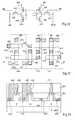
- Figures 1 and 2are respectively a view of above and in sectional view of an example of a portion of a circuit conventional integrated circuit formed in a semiconductor substrate.
- recessesare formed on the surface of the substrate 1. These recesses are filled with an insulating material.
- the filled recesses of insulationare commonly called isolation areas STI, from English Shallow Trench Isolation.
- the isolation areasare hatched.
- the portions of the surrounding substrate or surrounded by isolation areasconstitute areas active.
- two zones square insulation 2 and 3are separated by an active zone 4.
- Two rectangular active zones 5 and 6are placed in each of the isolation zones 2 and 3.
- the zones isolation 2, 3 and the active zone 4are surrounded by a zone active substantially rectangular 7.
- An isolation zone 8surrounds the active area 7.
- a silicon area polycrystalline 9, shown in dashed lines in the figure 1,is placed perpendicular to the portion of the active zone 7 shown on the right of Figure 1.
- Area 9is separated from active zone 7 and isolation zones 3 and 8 by a thin layer of oxide.
- Zone 9is the grid of a MOS transistor whose source and drain are formed in the area active 7 on each side of zone 9.
- Substrate 1 and isolation areas 2, 3 and 8are covered with an insulating layer 10.
- a contact 11is placed in an opening of the insulation layer 10 above the active zone 4.
- a contact 12is placed in an opening of the insulating layer 10 above the polycrystalline silicon zone 9.
- the contacts 11 and 12make it possible to connect the active zone 4 and the zone of polycrystalline silicon 9 to a component of the integrated circuit or a power supply terminal via a network interconnection, not shown, placed above the layer insulation 10.
- FIG. 3is a sectional view of an example of integrated circuit according to the present invention, the view of which above is identical to that shown in Figure 1. The view in section is performed as for Figure 2 along the axis AA '.
- the integrated circuit of the present inventioncomprises conductive regions 20 and 21 embedded in the zones 2 and 3, and thus isolated from the substrate 1. In this For example, no conductive region is placed inside the isolation area 8.
- a contact 22is placed in two superposed openings the insulating layer 10 and the portion of the zone 2 above the conductive layer 20.
- a contact 23, represented by a cross in a dashed square in FIG. 1,is placed in two superposed openings of the insulating layer 10 and the right portion of the zone 3 above the conductive layer 21.
- the contacts 22 and 23are connected to the non-interconnection network represent.
- the conductive layers 20 and 21are thus connected each at a reference voltage, for example a voltage supply and ground, via contacts 22 and 23.
- a contact 24is placed in two openings superimposed of the insulating layer 10 and the right portion of the isolation zone 2.
- the opening of the insulating layer 10is carried out over the left side of the isolation area 2 and above the right part of the active zone.
- a contact 25is placed in two superposed openings the insulating layer 10 and the left portion of the zone Isolation 3.
- the opening of the insulating layer 10is achieved above the right side of the left portion of the area Isolation 3 and above the left part of the active zone 6.
- a contact 26is placed in two superposed openings of the insulating layer 10 and the right portion of the isolation zone 3.
- the opening of the insulating layer 10is made above and to the side of the left side of the polycrystalline silicon zone 9.
- the contact 26thus makes it possible to connect the conductive layer 21 to the grid zone 9 of the transistor.
- an integrated circuitincludes conductive regions placed within certain isolation areas surrounding or surrounded by active.
- the conductive regionsare biased to a voltage reference and linked to selected regions of one or more components of an integrated circuit through a contact placed above the conductive regions.
- An advantage of an integrated circuit structure according to the present inventionis that it makes it possible to integrate a network of distribution of reference voltages in an integrated circuit without changing its structure, that is to say without increasing the number of levels of the interconnection network and without reducing the density of integration of components in the substrate.
- the present inventionfurther provides a method of realization of an integrated circuit comprising as the circuit of FIG. 3 conductive lines buried in the zones isolation formed in the circuit substrate.
- recesses 102 and 103are formed in a substrate 101, for example made of monocrystalline silicon.
- the recesses 102 and 103are separated by a portion of substrate corresponding to an active zone 104. and the walls of the recesses 102 and 103 are respectively covered with insulating layers 106 and 107.
- the insulating layers 106 and 107may consist of a single insulator or of several insulators such as silicon oxide (SiO 2 ) and silicon nitride (Si 3 N 4 ).
- a sacrificial layer 110, 111made of a material selectively etchable by to the substrate 101 and the insulators 106 and 107. It will be possible example to form silicon / germanium sacrificial layers when the substrate is silicon.
- a method of training layers 110 and 111consists of producing a silicon / germanium deposit on the entire structure so as to fill completely the recesses 102 and 103, then to polish the silicon / germanium according to a standard polishing process chemical mechanics until discovering the upper surface of the substrate 101, and finally to perform a partial etching of portions of silicon / germanium filling the recesses 102 and 103 so as to keep a layer of silicon / germanium in the bottom of each of the recesses.
- an insulating layer in each of the recesses 102 and 103In the next step, illustrated in FIG. an insulating layer in each of the recesses 102 and 103.
- the intermediate layers 110 and 111are thus covered respectively insulating layers 120 and 121.
- a method of formation of the insulating layers 120 and 121is to perform an insulation deposit on the entire structure so as to completely fill the recesses 102 and 103 and perform a mechanical-chemical polishing of the deposited insulation to discover the upper surface of the substrate 101.
- the insulating layers 106 and 120belong to a portion 125 of an isolation area.
- the layers insulators 107 and 121belong to a portion 126 of an area isolation. Portions 125 and 126 may belong to different isolation areas or in the same isolation zone as will appear in the following description in relation Figures 11 and 12.
- a MOS transistor 130is formed.
- Source / drain areas 131 and 132are respectively formed close to isolation areas 125 and 126.
- the portion of the substrate 101 placed between the source / drain zones 131 and 132is covered with a gate oxide 133 itself covered with a grid 134.
- Insulating spacers 135 and 136are formed on the flanks of the grid 134. We then cover the whole of the structure of an insulating protective layer 138.
- openings in the insulating layer 138 and in the layers insulators 120 and 121for example by etching.
- an opening O1is formed in the insulating layers 138 and 120 above the middle layer 110 so as to discover a central portion of the layer 110.
- An O2 openingis formed in the insulating layer 138 above the source / drain zone 131.
- An opening O3is formed in the insulating layers 138 and 121 above the source / drain zone 132 and the zone 126 to discover a portion of the source / drain 132, the upper surface of the insulating layer 107 and a portion of the intermediate layer 111.
- the areas of the insulating layers 106 and 107 discovered by this stage of engravingmust be made of an insulation different from that of the layers insulators 138, 120 and 121 so as not to be etched during the formation of the openings O1, O2 and O3.
- the layers 110 and 111are silicon / germanium and the silicon substrate, an etching process is chosen selective silicon / germanium with respect to silicon.
- "tunnels"were formed under the insulating layers 120 and 121.
- the contact C1is then connected, for example, to a reference potential and the contact C3 is then connected to a component of the integrated circuit formed in the substrate 101 or at a integrated circuit terminal via a network interconnection, not shown, which is formed above the insulating layer 138.
- the layers 110 and 111 deposited at the bottom of recessesare no longer sacrificial layers but final.
- the layers 110 and 111then consist of a conductive material. Once the openings formed above conductive layers, a metal contact is directly formed in the opening.
- This variantis simpler but it is not recommended in the case where the conductive material does not can withstand the high temperatures of the production steps components.
- the materialshould not be susceptible to diffuse into the substrate during these high steps temperature so as not to damage the circuit components integrated. For example, it will be possible to form layers 110 and 111 in titanium nitride which is a stable material.
- Figures 11 and 12are two examples of above the structure shown in Figure 10.
- the active area 4is a small rectangular area.
- the grid 134shown in dotted lines, is placed perpendicularly to the active zone 4.
- the C2 contactis placed above active area 4.
- the structure of Figure 11includes an isolation zone 150 rectangular surrounding the active area 4.
- a thin active zone 151surrounds the isolation zone 150 which is itself surrounded by an isolation zone 152.
- the contact C1is placed above the isolation zone 150 in the extension active zone 4.
- the contact C3is placed above the active zone 4 and the isolation zone 150.
- the two portions of isolation areas 125 and 126 placed under the contacts C1 and C3belong to the same zone Isolation 150
- the structure of Figure 12includes two areas substantially rectangular isolation 160 and 161 from each other by a thin rectangular active zone 162.
- the isolation area 160surrounds partially active area 4.
- Isolation areas 160 and 161are surrounded by a thin active zone 163, itself surrounded by an isolation zone 164.
- the C1 contactis placed above of the isolation zone 160 in the extension of the zone active 4 on the opposite side to the active area 162.
- the contact C3is placed above active zone 4 and the isolation zone 161.
- the two portions of the zone 125 and 126 placed under contacts C1 and C3belong to different isolation areas.
- Figures 13 to 20are sectional views of structures obtained after different stages of a setting mode of the method of the present invention integrated with a standard procedure for making isolated isolation zones deep, better known as the STI of English Shallow Trench Isolation.
- the traditional STI training processis to oxidize a silicon substrate to form a thin layer of silicon oxide that is covered with a layer nitride then a layer of a mask constituted for example of densified silicon oxide (TEOS).
- the maskis then covered with a layer of photosensitive resin that we insole and develops to define areas where we want to achieve a recess of the substrate.
- a series of successive engravings of the mask, the nitride layer, the thin layer of silicon oxide and the substratewe removes the resin and the mask.
- Figure 13is a sectional view of a structure obtained after all the operations described above.
- a recess 200is formed in a substrate 201.
- the bottom and the walls of the recess 200are covered with a thin layer silicon oxide 202.
- the substrate 201is covered with a layer of silicon oxide 203 itself covered with a nitride layer 204.
- spacers 210 and 211nitride against the walls of the recess 200.
- the spacers 210 and 211are for example formed by a conventional method of performing a nitrile deposit and then perform an anisotropic etching of nitride so in this example to discover the thin layer silicon oxide 202 at the bottom of the recess 200.
- Insulation depositedis conventionally silicon oxide deposited according to a mixed deposition / etching technique to avoid training of "holes".
- a chemical-mechanical polishing of the insulating layer 230 to discover the nitride layer 204anisotropic etching of the nitride layer 204 and spacers 210 and 211 to discover the silicon oxide layer 203.
- a silicon oxide etchingis then carried out completely eliminate the silicon oxide layer 203.
- Componentsare then made in and above active regions of the substrate 201, not shown, separated each other by recesses identical to the recess 200.
- an opening 04is etched in the insulating layers 240 and 230 above a portion of the substrate 201, the spacer 211 and a portion of the intermediate layer 220.
- conductive layer 250at the bottom of the recess 200 and a contact 251 in the opening 04.
- the conductive layer 250is connected to a portion of the substrate via the contact 251.
- steps previously described in relation to FIGS. 14, 15, 18, 19 and 20are in addition to the steps of the method standard formation of shallow isolation areas or STIs. These additional steps can be implemented on any or part of the integrated circuit. If you want to form lines buried only in part of the isolation areas of the circuit, it is necessary to provide additional steps “masking” and “unmasking” of the isolation zones where one do not want to incorporate buried lines.
- An embodiment of an integrated circuit according to the present inventionis an SRAM type memory described below.
- FIG 21is a typical diagram of a point SRAM memory.
- the memory pointincludes two inverters 300 and 301 each composed of a PMOS transistor 302 and 303 and a NMOS transistor 304 and 305.
- the gates of transistors 302 and 305 304 of the inverter 300are interconnected and connected to the drains transistors 303 and 305 of the inverter 301.
- the gates of the transistors 303 and 305 of the inverter 301are interconnected and connected to the drains of transistors 302 and 304 of the inverter 300.
- the sources of the PMOS transistors 302 and 303are connected to a supply voltage Vdd.
- the sources NMOS transistors 304 and 305are connected to ground GND.
- the drains transistors 302 and 304are connected to a bit line BL via an NMOS transistor 306. Similarly, the drains of the transistors 303 and 305 are connected to a bit line complementary BLN via an NMOS transistor 307. The gates of the transistors 306 and 307 are connected to a line row RL.
- An SRAM memoryconventionally comprises a matrix of memory points such as that of Figure 21 that one can select by means of several rows of rows and several pairs of BL / BLN bit lines. Operation such an SRAM is known and will not be described in detail.
- Figure 22is a schematic top view of the SRAM memory point of Figure 21.
- the memory pointis formed in a P-type substrate. Active areas of the substrate are represented by vertical rectangles. Grids of Transistors are represented by horizontal rectangles. Isolated areas are formed wherever not represented active areas. Contacts are represented by a square or a rectangle in which is placed a cross.
- an NMOS transistor or PMOSis constituted a vertical active zone and a horizontal grid zone intersecting perpendicularly.
- portions of the active area located on either side of the gate areaare doped type N.
- portions of the active zone located on either side of the gate areaare p-type doped.
- Active areas corresponding to NMOS transistors 304 and 306constitute a single rectangular active area vertical 400 placed on the left of Figure 22 inside a box area P 410 shown in dotted lines.
- the active areas of NMOS transistors 305 and 307constitute a single active zone 401 of the same shape as the zone 400 but placed on the right of Figure 22 within a zone of box P 411 shown in dotted lines.
- Two active zones 402 and 403 corresponding to PMOS transistors 302 and 303are placed between the active zones 400 and 401 inside a box area N 412 shown in dotted lines.
- Active area 402 corresponding to the PMOS transistor 302is placed at the bottom to left of box area N 410 and corresponding area 403 to the PMOS transistor 303 is placed at the top right of the box N 412.
- a grid area 420corresponding to the grid of the transistor 306, intersects the active zone 400 on the top of the Fig.
- a grid area 421, corresponding to the grid of transistors 302 and 304,is placed perpendicular to the zones active 400 and 402 on the bottom of the figure.
- a grid area 422, corresponding to the gate of transistor 307intersects the zone 401 on the bottom of the figure.
- a grid area 423, corresponding to the gates of the transistors 303 and 305,is placed perpendicular to the active areas 401 and 403 on the top of the figure.
- Two contacts 430 and 431are respectively placed on the left of zone 420 and on the right of zone 422.
- the contacts 430 and 431make it possible to connect the grids of the transistors 306 and 307 at row line RL not shown.
- Two contacts 432 and 433 placed respectively on the top of the zone 400 and on the bottom of zone 401make it possible to connect the transistors 306 and 307 at the bit lines BL and BLN.
- Three contacts 434, 435 and 436 placed respectively at middle of active area 400, on top of active area 402 and on the left of the active zone 423,are connected together by via a metal connection not shown.
- a contact 440is placed above the lower portion of the active zone 400 and extends to the left above an isolation area.
- a contact 441is placed above the lower portion of the active area 402 and extends to the left over an area isolation.
- a contact 442is placed above the portion upper active area 401 and extends to the right above an isolation zone.
- a 443 contactis placed above of the upper portion of the active zone 403 and extends on the right above an isolation area.
- FIG. 23is a sectional view of the memory point represented in FIG. 23 along an axis B-B 'cutting the contacts 440, 441 and 433.
- the active zones 400, 402 and 401are formed at the surface of the P-type substrate 450.
- the active zones 400, 401 and 402are separated by portions of isolation areas.
- a conductive regionis placed inside each of the zones isolation.
- Four portions of isolation areas 451, 452, 453 and 454are visible from left to right.
- the regions conductors placed in portions 452 and 453 respectively between active zones 400 and 402 and between active zones 402 and 401are both connected to a supply voltage Vdd.
- the conductive regions placed in the portions 451 and 454 respectively to the left of the active zone 400 and to the right of the active zone 401are both connected to GND mass.
- the N-type caisson 412is placed under the zone active 402 and under a portion of isolation areas 452 and 453.
- the casings of type P 410 and 411are placed respectively at left and right of the N-type well 412.
- the isolation areas and the active areasare covered with an insulating layer 455.
- Contacts 440, 441 and 433are placed in openings of the insulating layer 455.
- the contact 440covers the area active 400, the insulating layer placed against the walls of the isolation zone 451 and the conductive region connected to GND within the isolation area 451.
- the portion of the active zone 400 corresponding to the source of the transistor 304is thus connected to the ground GND via the contact 440.
- the contact 441covers the active zone 402, the insulating layer placed against the walls of the isolation zone 452 and the conductive region connected to Vdd placed at the bottom of the same zone 452.
- the portion of the active zone 402 corresponding to the source of the transistor 302is thus connected to the power supply Vdd via contact 441.
- Contact 433is placed conventionally above the portion of the active zone 401 corresponding to a source / drain zone of transistor 307.
- Figure 24is a schematic top view of a portion of an SRAM consisting of a set of points memory of composition identical to that of the memory point described in relation to Figures 21 to 23.
- the memory pointsare placed next to each other so as to form rows and columns of memory points.
- four points memory P1 to P4are shown.
- the point P1is represented in bottom left of the figure with structure and orientation identical to the memory point represented in FIG. has a symmetrical structure of the point P1 with respect to an axis horizontal.
- Point P2is placed above point P1 so that the contacts 432, 433 and 442 of each of the points are like superimposed and in fact constitute only three contacts.
- the point P3has a structure symmetrical to that of point P1 by relative to a vertical axis.
- Point P3is placed to the right of point P1 so that the contacts 431 of each of the points are superimposed and constitute one and the same contact, and so that contacts 442 are contiguous.
- Point P4has a structure symmetrical with that of point P3 with respect to a horizontal axis. The point P4 is placed above the point P3 so that their contacts 432, 443 and 442 are "superimposed”. In addition, point P4 is placed to the right of point P2 so their contacts 431 are "superimposed” and their contacts 442 are contiguous.
- the pairs of points P1 / P2 and P3 / P4belong respectively to two different vertical columns.
- the pairs of points P1 / P3 and P2 / P4belong to two different horizontal rows.
- the points P1 to P4belong to both upper rows of memory and to the two most columns to the right of the memory.
- the active zones 400 of the points P3 and P4are contiguous to one another so as to form a line continuous vertical active L1-400 which is extended downwards by zones 400 other memory points not shown of the same column.
- the areas 401 of the points P3 and P4are joined to each other so as to form an active line continuous vertical L1-401 which is extended downwards by zones 401 other memory points of the same column.
- zones 400 and 401 of points P3 and P4constitute also continuous vertical lines L2-400 and L2-401 that extend down.
- Isolated areas between the vertical active lines L1-400 and L1-401constitute in fact one and the same isolation zone whose region conductive substantially has the shape of a rail connected to Vdd.
- the isolation areas located between the vertical lines active L2-401 and L2-400constitute a single zone insulation whose conductive region has substantially the shape a rail connected to Vdd.
- the isolation areas located between vertical active lines L1-401 and L2-401constitute a single and unique isolation zone whose conductive region has substantially the shape of a rail connected to GND.
- the Vdd and GND railsend at the bottom and top of each column of the SRAM.
- Two structures "off"are placed at the top and bottom of the SRAM.
- the two structuresare symmetrical to each other with respect to a horizontal axis.
- the upper stop structureis shown in figure 24. It includes four rectangular active zones vertical lines 501, 502, 503 and 504 extending the lines vertical active L1-400, L1-401, L2-401 and L2-400 to the high.
- a horizontal active zone 505is contiguous to the part of each of the active zones 501 to 504.
- the rails Vdd and GNDthus end at active area 505.
- active areas 501 to 505are N-doped and connected to the mass.
- a gate area 506intersects the active areas 502 and 503 perpendicularly above the contacts 433 of the points P2 and P4.
- a contact 507is placed above the portion of an isolation zone delimited vertically by active zones 502 and 503 and bounded horizontally by the active area 505 and gate area 506.
- Contact 507extends above active area 505 and above the area of gate 506.
- the contact 507connects the mass GND to the active zone 505, to the gate area 506 and to the GND rail placed in the portion of the isolation area mentioned above.
- Transistors NMOS sharing the same grid area 506are still no conductors, which isolates the BLN bit lines from the mass.
- the N-type casings 412 of each of the memory pointsare contiguous to each other to form a single N type vertical box.
- P-type caissons 410 and 411 of two adjacent columnsform a single vertical p-type box.
- the boxes N 412 points P2 and P4extend upward respectively by boxes 508 and 509.
- Active areas 510 and 511are placed inside the boxes N 508 and 509.
- Contacts 512 and 513are placed perpendicular to the active areas 510 and 511.
- a continuous vertical active lineis placed from each side of the memory.
- an active line vertical 516is placed to the right of the contacts 430 of the points P3 and P4.
- the upper part of the vertical active line 516is contiguous to the active zone 505.
- the zone-conducting regions isolated between the memory points and these lines vertical active elementsconstitute two GND rails.
- Contact 515is extend in this example to above the active line 516. The contact 515 makes it possible to connect to the ground the zones 516, 501 and 505 and the GND rail to the right of Memory.
- FIG. 25is a schematic top view of a another portion of the SRAM memory described above.
- the length of the vertical rails GND and Vdd as well as caissons N and Pcan be important. It is then necessary to provide additional feed points from each of the rails and boxes by inserting for example relay blocks between two rows of memory.
- Two points memory P5 and P6 belonging to the same roware represented on the bottom of the figure.
- the point P5has a structure and a orientation identical to that of the memory point represented in Figure 22.
- the point P6has a structure symmetrical to that of the point P5 with respect to a vertical axis.
- Points P5 and P6are wedged to each other so their contacts 431 constitute one and the same contact and that their contacts 442 are contiguous to each other.
- two points memory P7 and P8 belonging to the same roware represented on the top of the figure.
- Point P7has a symmetrical structure that of the point P5 with respect to a horizontal axis.
- Point P8has a structure symmetrical to that of point P7 with respect to a vertical axis.
- the points P7 and P8are contiguous to each other so that their 431 contacts constitute one and the same contact and their contacts 442 are contiguous.
- the two rows representedare connected to the other by a relay block described below.
- Active areas 400 points P5 and P7are connected by an active zone 530. From same, the active areas 400 of the points P6 and P8 are connected by active zone 531. Active zones 401 of points P5 and P7 are connected by an active zone 532. The active zones 401 of the points P6 and P8 are connected by an active zone 533.
- the zones 530, 531, 532 and 533are N-type doped.
- N 412 pairs of points P5 / P7 and P6 / P8are connected respectively by caissons N 534 and 535.
- the caissons P of points P5 / P7 and P6 / P8are similarly connected by caissons P.
- Active zones 536 and 537are placed at the interior of the caissons N 534 and 535.
- Contacts 538 and 539are placed perpendicularly to the active areas 536 and 537. Being connected to the Vdd power supply, contacts 538 and 539 allow to feed the N type caissons 534 and 535 and that the Vdd rails placed inside the isolation areas surrounding active areas 536 and 537.
- a 540 contactis placed above active area 530 and extends to the left.
- a contact 541is placed above active area 531 and extend to the right. Being connected to the GND mass, the contacts 540 and 541 make it possible to polarize the GND rails placed respectively within the isolation areas located on the left of the points P5 / P7 and on the right of the points P6 / P8.
- two grid areas 542 and 543are placed perpendicularly active zones 532 and 533.
- An active zone 545is placed between the grid areas 542 and 543 and connects the active zones 532 and 533.
- Active zone 545is doped with P-type unlike the active zones 532 and 533 which are doped with type N.
- a contact 546is placed above the active zone 545 and extends above the isolation areas below and over active area 545 and extends above grid areas 542 and 543. The contact 546 is connected to the mass.
- the contact 546makes it possible to polarize the P boxes under the active zone 545 and the GND rail placed inside the isolation areas covered by the contact 546.
- the four NMOS transistors formed by the zones of grid 442, 443 and active areas 432 and 433are all non drivers because their grids are grounded.
- An advantage of an SRAM memory as described previouslyis that the distribution network of voltages of reference Vdd and GND is placed in isolation areas. The component integration density is unchanged and the space available for rows of rows and bit lines is greatly increased.
- distribution networkscan serve to convey any reference voltage of a circuit integrated.
Landscapes
- Engineering & Computer Science (AREA)
- Physics & Mathematics (AREA)
- Condensed Matter Physics & Semiconductors (AREA)
- General Physics & Mathematics (AREA)
- Computer Hardware Design (AREA)
- Microelectronics & Electronic Packaging (AREA)
- Power Engineering (AREA)
- Manufacturing & Machinery (AREA)
- Semiconductor Memories (AREA)
- Element Separation (AREA)
Abstract
Translated fromFrenchDescription
Translated fromFrenchLa présente invention concerne les circuits intégréset plus particulièrement les réseaux de distribution d'unetension de référence telle qu'une tension d'alimentation ou lamasse.The present invention relates to integrated circuitsand more particularly the distribution networks of areference voltage such as a supply voltage or themass.
Un circuit intégré comprend de façon générale un réseaude distribution de la tension d'alimentation Vdd, un réseau dedistribution de la masse GND, et éventuellement des réseaux dedistribution d'autres tensions de référence, par exemple Vdd/2,formés au-dessus du circuit intégré. Les lignes conductrices desréseaux de distribution font partie des lignes conductrices duréseau d'interconnexion du circuit intégré. Les lignes conductricesdu réseau d'interconnexion sont formées sur plusieursniveaux et sont reliées les unes aux autres par des vias conducteurs.Chacun de ces réseaux de distribution est généralementconstitué de rails parallèles relativement longs et largesformés sur un des niveaux du réseau d'interconnexion du circuitintégré. L'espace occupé par les lignes de ces réseaux dedistribution est relativement important ce qui a pour effet delimiter l'espace disponible pour les autres lignes du circuitgénéralement destinées à transmettre des signaux. Or la faibleplace disponible pour ces lignes fait qu'elles sont souventétroites et qu'elles présentent en conséquence une résistance relativement importante qui est préjudiciable dans certainscircuits tels que des mémoires.An integrated circuit generally comprises a networkdistribution of the supply voltage Vdd, a network ofdistribution of the GND mass, and possibly networks ofdistribution of other reference voltages, for example Vdd / 2,formed above the integrated circuit. The conductive lines of thedistribution networks are part of the conductive lines of theinterconnection network of the integrated circuit. Conductive linesof the interconnection network are formed over severallevels and are connected to each other by conductive vias.Each of these distribution networks is generallyconsisting of relatively long and wide parallel railsformed on one of the levels of the circuit interconnection networkintegrated. The space occupied by the lines of these networks ofdistribution is relatively large which has the effect oflimit the space available for the other lines of the circuitgenerally intended to transmit signals. But the weakavailable space for these lines makes that they are oftennarrow and therefore have resistancerelatively important which is detrimental in somecircuits such as memories.
De façon générale, la distribution de tensions deréférence nécessite de prévoir des lignes conductrices forméessur les différents niveaux du réseau d'interconnexion. L'espaceoccupé par ces lignes conductrices de distribution peut devenirimportant, ce qui est préjudiciable à la réalisation de connexionsdestinées à transmettre des signaux.In general, the distribution of tensions ofreference requires the provision of conductive lines formedon the different levels of the interconnection network. Spaceoccupied by these conductive distribution lines can becomeimportant, which is detrimental to making connectionsfor transmitting signals.
Un moyen pour augmenter l'espace disponible pour leslignes de connexion "critiques" consiste à augmenter le nombrede niveaux du réseau d'interconnexion. Cette solution estnéanmoins coûteuse. Un autre moyen consiste à diminuer la densitéd'intégration de composants dans le substrat du circuitintégré afin de disposer de davantage d'espace au-dessus descomposants mais cette solution va à l'encontre de l'évolution dela technologie.A way to increase the space available for"critical" connection lines is to increase the numberlevels of the interconnection network. This solution isnevertheless expensive. Another way is to decrease the densitycomponent integration into the circuit substrateintegrated in order to have more space abovecomponents but this solution goes against the evolution oftechnology.
Un objet de la présente invention est de prévoir unestructure de lignes conductrices dédiées à la distribution d'unetension de référence qui permette d'augmenter de façon significativel'espace disponible pour la réalisation des connexionsdestinées à transmettre des signaux.An object of the present invention is to provide astructure of conductive lines dedicated to the distribution of areference voltage which allows to increase significantlythe space available for making connectionsfor transmitting signals.
Un autre objet de la présente invention est de prévoirun procédé de réalisation de telles lignes conductrices dédiéesà la distribution de tensions de référence.Another object of the present invention is to providea method of producing such dedicated conductive linesto the distribution of reference voltages.
Pour atteindre ces objets, la présente invention prévoitun circuit intégré comprenant un substrat semiconducteur danslequel des zones actives entourent ou sont entourées par desévidements remplis d'isolant, et dans lequel une région conductriceest noyée dans l'isolant d'au moins un évidement, la régionconductrice étant connectée à une tension de référence et étantconnectée à au moins un élément voisin du circuit.To achieve these objects, the present invention providesan integrated circuit comprising a semiconductor substrate inwhich active areas surround or are surrounded byrecesses filled with insulation, and wherein a conductive regionis embedded in the insulation of at least one recess, the regionconductor being connected to a reference voltage and beingconnected to at least one neighboring element of the circuit.
Selon un mode de réalisation du circuit intégrésusmentionné, la région conductrice est connectée à une ligneconductrice d'alimentation ou de masse d'un réseau d'interconnexion.According to an embodiment of the integrated circuitaforementioned, the conductive region is connected to a linesupply or ground conductor of an interconnection network.
Selon un mode de réalisation du circuit intégrésusmentionné, ledit élément du circuit est une borne d'uncomposant ou une prise de polarisation du substrat ou d'uncaisson formé dans le substrat.According to an embodiment of the integrated circuitaforementioned, said circuit element is a terminal of acomponent or polarization outlet of the substrate or acaisson formed in the substrate.
Selon un mode de réalisation du circuit intégrésusmentionné, le circuit comprend des composants formés dans deszones actives, le substrat et les composants étant recouvertsd'une couche isolante de protection, une portion d'une zoneactive adjacente à un desdits au moins un évidement étant reliéeà la région conductrice de cet évidement par l'intermédiaired'un contact métallique placé dans une unique ouverture de lacouche isolante de protection et de l'isolant recouvrant larégion conductrice.According to an embodiment of the integrated circuitmentioned above, the circuit comprises components formed inactive areas, the substrate and components being coveredan insulating protective layer, a portion of an areaactive adjacent to one of said at least one recess being connectedto the conductive region of this recess viaof a metallic contact placed in a single opening of theinsulating protective layer and insulation covering theconductive region.
Selon un mode de réalisation du circuit intégrésusmentionné, le substrat semiconducteur est en siliciummonocristallin, ledit isolant étant constitué d'oxyde de siliciumet de nitrure.According to an embodiment of the integrated circuitmentioned above, the semiconductor substrate is siliconmonocrystalline, said insulator consisting of silicon oxideand nitride.
Selon un mode de réalisation du circuit intégrésusmentionné, le circuit constitue une mémoire de type SRAM,dans laquelle le réseau de distribution des tensions d'alimentationet de masse est constitué d'un réseau de régions conductricesnoyées dans plusieurs évidements du substrat, les régionsconductrices étant reliées à plusieurs zones de source/drain destransistors MOS de la mémoire par des contacts.According to an embodiment of the integrated circuitmentioned above, the circuit constitutes an SRAM type memory,in which the distribution network of the supply voltagesand mass consists of a network of conductive regionsembedded in several recesses of the substrate, the regionsconductors being connected to several source / drain areas ofMOS transistors of the memory by contacts.
La présente invention prévoit aussi un procédé deréalisation de lignes conductrices enterrées dans un substratd'un circuit intégré, comprenant les étapes suivantes : formerdes évidements dans un substrat semiconducteur et recouvrir lefond et les parois d'isolant ; former au fond des évidements descouches d'un matériau sacrificiel ; remplir les évidements d'unisolant pour former des couches isolantes au-dessus des couchesdudit matériau sacrificiel ; former des ouvertures dans lescouches isolantes ; éliminer ledit matériau sacrificiel ; etremplir d'un matériau conducteur les ouvertures et l'espaceprécédemment occupé par ledit matériau sacrificiel.The present invention also provides a method ofproduction of conductive lines buried in a substrateof an integrated circuit, comprising the following steps: formingrecesses in a semiconductor substrate and cover thebottom and walls of insulation; to form deep recesseslayers of sacrificial material; fill in the recesses of ainsulation to form insulating layers above the layerssaid sacrificial material; form openings in theinsulating layers; removing said sacrificial material; andfill the openings and the space with conductive materialpreviously occupied by said sacrificial material.
Selon un mode de mise en oeuvre du procédé susmentionné,le procédé comprend, à la suite de la troisième étape,les étapes suivantes : former des composants dans certaineszones actives du substrat ; recouvrir le substrat et les composantsd'une couche isolante de protection ; et former des ouverturesdans la couche isolante de protection et dans les couchesisolantes.According to one embodiment of the aforementioned method,the process comprises, following the third step,the following steps: forming components in certainactive areas of the substrate; cover the substrate and componentsan insulating protective layer; and form openingsin the protective insulating layer and in the layersinsulating.
Ces objets, caractéristiques et avantages, ainsi qued'autres de la présente invention seront exposés en détail dansla description suivante de modes de réalisation particuliersfaite à titre non-limitatif en relation avec les figures jointesparmi lesquelles :
Par souci de clarté, de mêmes éléments ont été désignéspar de mêmes références aux différentes figures. En outre,comme cela est courant dans la représentation des circuitsintégrés, les figures 1 à 20, 22 et 23 ne sont pas tracées àl'échelle.For the sake of clarity, the same elements have been designatedby same references to the different figures. In addition,as is common in circuit representationfigures 1 to 20, 22 and 23 are not shown inthe scale.
Les figures 1 et 2 sont respectivement une vue dedessus et en vue en coupe d'un exemple de portion d'un circuitintégré classique formé dans un substrat semiconducteur 1. Desévidements sont formés en surface du substrat 1. Ces évidementssont remplis d'un matériau isolant. Les évidements remplisd'isolant constituent des zones d'isolement couramment appeléesSTI, de l'anglais Shallow Trench Isolation. Les zones d'isolementsont hachurées. Les portions du substrat entourant ouentourées par des zones d'isolement constituent des zonesactives. Dans cet exemple de portion de circuit, deux zonesd'isolement carrées 2 et 3 sont séparées par une zone activerectangulaire 4. Deux zones actives rectangulaires 5 et 6 sontplacées dans chacune des zones d'isolement 2 et 3. Les zonesd'isolement 2, 3 et la zone active 4 sont entourées par une zoneactive sensiblement rectangulaire 7. Une zone d'isolement 8entoure la zone active 7. A titre d'exemple, une zone de siliciumpolycristallin 9, représentée en pointillés sur la figure1, est placée perpendiculairement à la portion de la zone active7 représentée sur la droite de la figure 1. La zone 9 estséparée de la zone active 7 et des zones d'isolement 3 et 8 parune fine couche d'oxyde. La zone 9 constitue la grille d'untransistor MOS dont les source et drain sont formés dans la zoneactive 7 de chaque côté de la zone 9.Figures 1 and 2 are respectively a view ofabove and in sectional view of an example of a portion of a circuitconventional integrated circuit formed in a semiconductor substrate.recesses are formed on the surface of the
Divers composants non représentés sont formés dans etau-dessus des zones actives. Le substrat 1 et les zones d'isolement2, 3 et 8 sont recouverts d'une couche isolante 10. A titred'exemple, un contact 11 est placé dans une ouverture de lacouche isolante 10 au-dessus de la zone active 4. De même, un contact 12 est placé dans une ouverture de la couche isolante 10au-dessus de la zone de silicium polycristallin 9. Les contacts11 et 12 permettent de relier la zone active 4 et la zone desilicium polycristallin 9 à un composant du circuit intégré ou àune borne d'alimentation par l'intermédiaire d'un réseaud'interconnexion, non représenté, placé au-dessus de la coucheisolante 10.Various components not shown are formed in andabove the active areas.
La figure 3 est une vue en coupe d'un exemple decircuit intégré selon la présente invention dont la vue dedessus est identique à celle représentée en figure 1. La vue encoupe est réalisée comme pour la figure 2 selon l'axe AA'.FIG. 3 is a sectional view of an example ofintegrated circuit according to the present invention, the view of whichabove is identical to that shown in Figure 1. The view insection is performed as for Figure 2 along the axis AA '.
Le circuit intégré de la présente invention comprenddes régions conductrices 20 et 21 noyées dans les zonesd'isolement 2 et 3, et donc isolées du substrat 1. Dans cetexemple, aucune région conductrice n'est placée à l'intérieur dela zone d'isolement 8.The integrated circuit of the present invention comprises
Un contact 22 est placé dans deux ouvertures superposéesde la couche isolante 10 et de la portion de la zoned'isolement 2 au-dessus de la couche conductrice 20. De même, uncontact 23, représenté par une croix dans un carré en pointilléssur la figure 1, est placé dans deux ouvertures superposées dela couche isolante 10 et de la portion de droite de la zoned'isolement 3 au-dessus de la couche conductrice 21. Lescontacts 22 et 23 sont reliés au réseau d'interconnexion nonreprésenté. Les couches conductrices 20 et 21 sont ainsi reliéeschacune à une tension de référence, par exemple une tensiond'alimentation et la masse, par l'intermédiaire des contacts 22et 23.A
En outre, un contact 24 est placé dans deux ouverturessuperposées de la couche isolante 10 et de la portion de droitede la zone d'isolement 2. L'ouverture de la couche isolante 10est réalisée au-dessus de la partie gauche de la zone d'isolement2 et au-dessus de la partie droite de la zone active 5. Demême, un contact 25 est placé dans deux ouvertures superposéesde la couche isolante 10 et de la portion de gauche de la zone d'isolement 3. L'ouverture de la couche isolante 10 est réaliséeau-dessus de la partie droite de la portion gauche de la zoned'isolement 3 et au-dessus de la partie gauche de la zone active6. Les contacts 24 et 25 permettent ainsi de relier les couchesconductrices 20 et 21 respectivement à des régions choisies deszones actives 5 et 6.In addition, a
Un contact 26 est placé dans deux ouvertures superposéesde la couche isolante 10 et de la portion de droite de lazone d'isolement 3. L'ouverture de la couche isolante 10 estréalisée au dessus et sur le côté de la partie de gauche de lazone de silicium polycristallin 9. Le contact 26 permet ainsi derelier la couche conductrice 21 à la zone 9 de grille dutransistor.A
Ainsi, un circuit intégré selon la présente inventioncomprend des régions conductrices placées à l'intérieur decertaines zones d'isolement entourant ou entourées par des zonesactives. Les régions conductrices sont polarisées à une tensionde référence et reliées à des régions choisies d'un ou plusieurscomposants d'un circuit intégré par l'intermédiaire d'un contactplacé au-dessus des régions conductrices.Thus, an integrated circuit according to the present inventionincludes conductive regions placed withincertain isolation areas surrounding or surrounded byactive. The conductive regions are biased to a voltagereference and linked to selected regions of one or morecomponents of an integrated circuit through a contactplaced above the conductive regions.
Un avantage d'une structure de circuit intégré selonla présente invention est qu'elle permet d'intégrer un réseau dedistribution de tensions de référence dans un circuit intégrésans modifier sa structure, c'est-à-dire sans augmenter lenombre de niveaux du réseau d'interconnexion et sans diminuer ladensité d'intégration de composants dans le substrat.An advantage of an integrated circuit structure according tothe present invention is that it makes it possible to integrate a network ofdistribution of reference voltages in an integrated circuitwithout changing its structure, that is to say without increasing thenumber of levels of the interconnection network and without reducing thedensity of integration of components in the substrate.
La présente invention prévoit en outre un procédé deréalisation d'un circuit intégré comprenant comme le circuit dela figure 3 des lignes conductrices enterrées dans les zonesd'isolement formées dans le substrat du circuit.The present invention further provides a method ofrealization of an integrated circuit comprising as the circuit ofFIG. 3 conductive lines buried in the zonesisolation formed in the circuit substrate.
Dans une première étape, illustrée en figure 4, onforme dans un substrat 101, par exemple en silicium monocristallin,des évidements 102 et 103. Les évidements 102 et 103sont séparés par une portion de substrat correspondant à unezone active 104. Le fond et les parois des évidements 102 et 103 sont recouverts respectivement de couches isolantes 106 et 107.Les couches isolantes 106 et 107 peuvent être constituées d'ununique isolant ou de plusieurs isolants tels que de l'oxyde desilicium (SiO2) et du nitrure de silicium (Si3N4).In a first step, illustrated in FIG. 4, recesses 102 and 103 are formed in a
A l'étape suivante, illustrée en figure 5, on formedans chacun des évidements 102 et 103 une couche sacrificielle110, 111, constituée d'un matériau gravable sélectivement parrapport au substrat 101 et aux isolants 106 et 107. On pourra parexemple former des couches sacrificielles en silicium/germaniumlorsque le substrat est en silicium. Un procédé de formation descouches 110 et 111 consiste à réaliser un dépôt de silicium/germaniumsur l'ensemble de la structure de façon à remplircomplètement les évidements 102 et 103, puis à polir lesilicium/germanium selon un procédé standard de polissagemécano-chimique jusqu'à découvrir la surface supérieure dusubstrat 101, et enfin à effectuer une gravure partielle desportions de silicium/germanium remplissant les évidements 102 et103 de façon à conserver une couche de silicium/germanium dansle fond de chacun des évidements.In the next step, illustrated in FIG.in each of the
A l'étape suivante, illustrée en figure 6, on formeune couche isolante dans chacun des évidements 102 et 103. Lescouches intermédiaires 110 et 111 sont ainsi recouvertesrespectivement de couches isolantes 120 et 121. Un procédé deformation des couches isolantes 120 et 121 consiste à effectuerun dépôt d'isolant sur l'ensemble de la structure de façon àremplir complètement les évidements 102 et 103 et à effectuer unpolissage mécano-chimique de l'isolant déposé afin de découvrirla surface supérieure du substrat 101. Afin d'assurer que lesévidements 102 et 103 sont bien remplis d'isolant, on pourrautiliser une technique mixte associant un dépôt et une gravurequi permet d'éviter que des "trous" ne se forment dans la couched'oxyde de silicium quand l'évidement est profond et pas trèslarge.In the next step, illustrated in FIG.an insulating layer in each of the
Les couches isolantes 106 et 120 appartiennent à uneportion 125 d'une zone d'isolement. De même, les couches isolantes 107 et 121 appartiennent à une portion 126 d'une zoned'isolement. Les portions 125 et 126 peuvent appartenir à deszones d'isolement différentes ou à une même zone d'isolementcomme cela apparaítra dans la suite de la description en relationaux figures 11 et 12.The insulating
A l'étape suivante, illustrée en figure 7, on forme defaçon classique des composants dans et au-dessus de la zoneactive 104. Dans cet exemple, on forme un transistor MOS 130.Des zones de source/drain 131 et 132 sont formées respectivementà proximité des zones d'isolement 125 et 126. La portion dusubstrat 101 placée entre les zones de source/drain 131 et 132est recouverte d'un oxyde de grille 133 lui-même recouvert d'unegrille 134. Des espaceurs isolants 135 et 136 sont formés surles flancs de la grille 134. On recouvre ensuite l'ensemble dela structure d'une couche isolante de protection 138.In the next step, illustrated in FIG.classic way of components in and above the areaIn this example, a
A l'étape suivante, illustrée en figure 8, on formedes ouvertures dans la couche isolante 138 et dans les couchesisolantes 120 et 121, par exemple par gravure. Dans cet exemple,on forme une ouverture O1 dans les couches isolantes 138 et 120au-dessus de la couche intermédiaire 110 de façon à découvrirune portion centrale de la couche 110. On forme une ouverture O2dans la couche isolante 138 au-dessus de la zone de source/drain131. On forme une ouverture O3 dans les couches isolantes 138 et121 au-dessus de la zone de source/drain 132 et de la zoned'isolement 126 de façon à découvrir une portion de la zone desource/drain 132, la surface supérieure de la couche isolante107 et une portion de la couche intermédiaire 111. Pour desraisons qui apparaítront ci-après, les zones des couches isolantes106 et 107 découvertes par cette étape de gravure doiventêtre constituées d'un isolant différent de celui des couchesisolantes 138, 120 et 121 afin de ne pas être gravées lors de laformation des ouvertures O1, O2 et O3.In the next step, illustrated in FIG.openings in the insulating
A l'étape suivante, illustrée en figure 9, on élimineles couches sacrificielles 110 et 111 par exemple par gravure.Dans le cas où les couches 110 et 111 sont en silicium/germanium et le substrat en silicium, on choisit un procédé de gravuresélectif du silicium/germanium par rapport au silicium. Al'issue de cette étape, on a formé des "tunnels" sous lescouches isolantes 120 et 121.In the next step, illustrated in FIG. 9, one eliminates
A l'étape suivante, illustrée en figure 10, on remplitles tunnels précédemment formés et les ouvertures O1, O2 et O3d'un matériau conducteur tel que de l'aluminium, du tungstène Wou du nitrure de titane TiN. On a ainsi formé des couchesconductrices 140 et 141 à l'intérieur des zones d'isolement 125et 126 ainsi que des contacts C1, C2 et C3 dans les ouverturesO1, O2 et O3. La couche conductrice 141 est ainsi reliée à lazone de source/drain 132 du transistor 130 par l'intermédiairedu contact C3. Comme cela a été précisé ci-dessus lors del'étape de gravure des ouvertures O1 à O3, la portion de lacouche isolante 107 placée contre la zone active 104 doit êtreconservée intacte afin d'éviter tout court-circuit entre lacouche conductrice 141 ou le contact C3 et le substrat 101.In the next step, illustrated in Figure 10, we fillpreviously formed tunnels and O1, O2 and O3 openingsa conductive material such as aluminum, tungsten Wor titanium nitride TiN. We have formed
Le contact C1 est alors connecté, par exemple, à unpotentiel de référence et le contact C3 est ensuite relié à uncomposant du circuit intégré formé dans le substrat 101 ou à uneborne du circuit intégré par l'intermédiaire d'un réseaud'interconnexion, non représenté, qui est formé au-dessus de lacouche isolante 138.The contact C1 is then connected, for example, to areference potential and the contact C3 is then connected to acomponent of the integrated circuit formed in the
Selon une variante du procédé de la présenteinvention, les couches 110 et 111 déposées au fond desévidements ne sont plus des couches sacrificielles maisdéfinitives. Les couches 110 et 111 sont alors constituées d'unmatériau conducteur. Une fois les ouvertures formées au-dessusdes couches conductrices, un contact métallique est directementformé dans l'ouverture. Cette variante est plus simple mais ellen'est pas conseillée dans le cas où le matériau conducteur nepeut résister aux températures élevées des étapes de réalisationdes composants. En outre, le matériau ne doit pas être susceptiblede diffuser dans le substrat lors de ces étapes hautetempérature afin de ne pas endommager les composants du circuit intégré. On pourra par exemple former des couches 110 et 111 ennitrure de titane qui est un matériau stable.According to a variant of the process of thisinvention, the
Les figures 11 et 12 sont deux exemples de vues dedessus de la structure représentée en figure 10. Dans les deuxfigures, la zone active 4 est une petite zone rectangulaire. Lagrille 134, représentée en pointillés, est placée perpendiculairementà la zone active 4. Le contact C2 est placé au-dessusde la zone active 4.Figures 11 and 12 are two examples ofabove the structure shown in Figure 10. In bothfigures, the
La structure de la figure 11 comprend une zone d'isolement150 rectangulaire entourant la zone active 4. Une finezone active 151 entoure la zone d'isolement 150 qui est elle-mêmeentourée par une zone d'isolement 152. Le contact C1 estplacé au-dessus de la zone d'isolement 150 dans le prolongementde la zone active 4. Le contact C3 est placé au-dessus de lazone active 4 et de la zone d'isolement 150. Dans cet exemple decircuit, les deux portions des zones d'isolement 125 et 126placées sous les contacts C1 et C3 appartiennent à la même zoned'isolement 150.The structure of Figure 11 includes an
La structure de la figure 12 comprend deux zonesd'isolement sensiblement rectangulaires 160 et 161 séparéesl'une de l'autre par une fine zone active rectangulaire 162. Undes côtés de la zone active 4, où est formée la zone desource/drain 132, est accolé à la zone active 162 du côté de lazone d'isolement 160. La zone d'isolement 160 entoure ainsipartiellement la zone active 4. Les zones d'isolement 160 et 161sont entourées par une fine zone active 163, elle-même entouréepar une zone d'isolement 164. Le contact C1 est placé au-dessusde la zone d'isolement 160 dans le prolongement de la zoneactive 4 du côté opposé à la zone active 162. Le contact C3 estplacé au-dessus de la zone active 4 et de la zone d'isolement161. Dans cet exemple de circuit, les deux portions de la zoned'isolement 125 et 126 placées sous les contacts C1 et C3appartiennent à des zones d'isolement différentes.The structure of Figure 12 includes two areassubstantially
Les figures 13 à 20 sont des vues en coupe destructures obtenues après différentes étapes d'un mode de mise en oeuvre du procédé de la présente invention intégré à unprocédé standard de réalisation de zones d'isolement peuprofondes, plus connues sous le nom de STI de l'anglais ShallowTrench Isolation. Le procédé classique de formation de STIconsiste à oxyder un substrat de silicium afin de former unefine couche d'oxyde de silicium que l'on recouvre d'une couchede nitrure puis d'une couche d'un masque constitué par exempled'oxyde de silicium densifié (TEOS). Le masque est ensuiterecouvert d'une couche de résine photosensible que l'on insoleet développe afin de définir des zones où l'on souhaite réaliserun évidement du substrat. On effectue ensuite une série degravures successivement du masque, de la couche de nitrure, dela fine couche d'oxyde de silicium et du substrat. Puis onélimine la résine et le masque. On fait croítre alors une couched'oxyde de silicium au fond et sur les parois des évidementsprécédemment formés dans le substrat.Figures 13 to 20 are sectional views ofstructures obtained after different stages of a setting modeof the method of the present invention integrated with astandard procedure for making isolated isolation zonesdeep, better known as the STI of English ShallowTrench Isolation. The traditional STI training processis to oxidize a silicon substrate to form athin layer of silicon oxide that is covered with a layernitride then a layer of a mask constituted for exampleof densified silicon oxide (TEOS). The mask is thencovered with a layer of photosensitive resin that we insoleand develops to define areas where we want to achievea recess of the substrate. Then a series ofsuccessive engravings of the mask, the nitride layer,the thin layer of silicon oxide and the substrate. Then weremoves the resin and the mask. We then grow a layerof silicon oxide at the bottom and on the walls of the recessespreviously formed in the substrate.
La figure 13 est une vue en coupe d'une structureobtenue après l'ensemble des opérations décrites ci-dessus. Unévidement 200 est formé dans un substrat 201. Le fond et lesparois de l'évidement 200 sont recouverts d'une fine couched'oxyde de silicium 202. Sur les bords de l'évidement 200, lesubstrat 201 est recouvert d'une couche d'oxyde de silicium 203elle-même recouverte d'une couche de nitrure 204.Figure 13 is a sectional view of a structureobtained after all the operations described above. A
A l'étape suivante, illustrée en figure 14, on formedes espaceurs 210 et 211 en nitrure contre les parois del'évidement 200. Les espaceurs 210 et 211 sont par exempleformés selon un procédé classique consistant à effectuer undépôt conforme de nitrure puis à réaliser une gravure anisotropedu nitrure de façon dans cet exemple à découvrir la fine couched'oxyde de silicium 202 au fond de l'évidement 200.In the next step, illustrated in FIG.
A l'étape suivante, illustrée en figure 15, on formeune couche intermédiaire 220, en silicium/germanium dans cetexemple, au fond de l'évidement 200 selon un procédé identique àcelui décrit en relation à la figure 5.In the next step, illustrated in FIG.an
A l'étape suivante, illustrée en figure 16, oneffectue un dépôt d'un isolant au-dessus de la structure defaçon à remplir intégralement l'évidement 200. L'isolant déposéest classiquement de l'oxyde de silicium déposé selon unetechnique mixte de dépôt/gravure permettant d'éviter la formationde "trous".In the next step, illustrated in Figure 16,makes a deposit of an insulator above the structure ofto completely fill the
A l'étape suivante, illustrée en figure 17, on réaliseun polissage mécano-chimique de la couche isolante 230 jusqu'àdécouvrir la couche de nitrure 204. On effectue ensuite unegravure anisotrope de la couche de nitrure 204 et des espaceurs210 et 211 jusqu'à découvrir la couche d'oxyde de silicium 203.On effectue ensuite une gravure d'oxyde de silicium jusqu'àéliminer complètement la couche d'oxyde de silicium 203. Lors deces deux gravures, l'épaisseur de la couche isolante 230 diminueplus ou moins en fonction des procédés de gravure mis en oeuvre.In the next step, illustrated in FIG.a chemical-mechanical polishing of the insulating
On réalise ensuite des composants dans et au-dessus dezones actives du substrat 201, non représentées, séparées lesunes des autres par des évidements identiques à l'évidement 200.Components are then made in and aboveactive regions of the
A l'étape suivante, illustrée en figure 18, onrecouvre l'ensemble de la structure d'une couche isolante 240.Puis on grave une ouverture 04 dans les couches isolantes 240 et230 au-dessus d'une portion du substrat 201, de l'espaceur 211et d'une portion de la couche intermédiaire 220.In the next step, illustrated in Figure 18,covers the entire structure of an insulating
A l'étape suivante, illustrée en figure 19, on éliminela couche intermédiaire 220 selon un procédé identique à celuidécrit en relation à la figure 9.In the next step, illustrated in Figure 19, we eliminatethe
A l'étape suivante, illustrée en figure 20, on remplitd'un matériau conducteur l'ouverture 04 ainsi que l'espaceprécédemment occupé par la couche 220. On a ainsi formé unecouche conductrice 250 au fond de l'évidement 200 et un contact251 dans l'ouverture 04. La couche conductrice 250 est reliée àune portion du substrat par l'intermédiaire du contact 251.In the next step, illustrated in FIG.of a conductive material the
Les étapes précédemment décrites en relation auxfigures 14, 15, 18, 19 et 20 s'ajoutent aux étapes du procédéstandard de formation de zones d'isolement peu profondes ou STI. Ces étapes additionnelles peuvent être mises en oeuvre sur toutou partie du circuit intégré. Si l'on souhaite former des lignesenterrées seulement dans une partie des zones d'isolement ducircuit, il est nécessaire de prévoir des étapes supplémentairesde "masquage" et de "démasquage" des zones d'isolement où l'onne souhaite pas incorporer de lignes enterrées.The steps previously described in relation toFIGS. 14, 15, 18, 19 and 20 are in addition to the steps of the methodstandard formation of shallow isolation areas or STIs.These additional steps can be implemented on anyor part of the integrated circuit. If you want to form linesburied only in part of the isolation areas of thecircuit, it is necessary to provide additional steps"masking" and "unmasking" of the isolation zones where onedo not want to incorporate buried lines.
Un exemple de réalisation d'un circuit intégré selonla présente invention est une mémoire de type SRAM décrite ci-après.An embodiment of an integrated circuit according tothe present invention is an SRAM type memory described below.
La figure 21 est un schéma classique d'un pointmémoire SRAM. Le point mémoire comprend deux inverseurs 300 et301 composés chacun d'un transistor PMOS 302 et 303 et d'untransistor NMOS 304 et 305. Les grilles des transistors 302 et304 de l'inverseur 300 sont reliées entre elles et reliées auxdrains des transistors 303 et 305 de l'inverseur 301. De même,les grilles des transistors 303 et 305 de l'inverseur 301 sontreliées entre elles et reliées aux drains des transistors 302 et304 de l'inverseur 300. Les sources des transistors PMOS 302 et303 sont reliées à une tension d'alimentation Vdd. Les sourcesdes transistors NMOS 304 et 305 sont reliées à la masse GND. Lesdrains des transistors 302 et 304 sont reliés à une ligne de bitBL par l'intermédiaire d'un transistor NMOS 306. De même, lesdrains des transistors 303 et 305 sont reliés à une ligne de bitcomplémentaire BLN par l'intermédiaire d'un transistor NMOS 307.Les grilles des transistors 306 et 307 sont reliés à une lignede rangée RL.Figure 21 is a typical diagram of a pointSRAM memory. The memory point includes two
Une mémoire SRAM comprend classiquement une matrice depoints mémoire tels que celui de la figure 21 que l'on peutsélectionner au moyen de plusieurs lignes de rangées et deplusieurs paires de lignes de bit BL/BLN. Le fonctionnementd'une telle mémoire SRAM est connu et ne sera pas décrit endétail.An SRAM memory conventionally comprises a matrix ofmemory points such as that of Figure 21 that one canselect by means of several rows of rows andseveral pairs of BL / BLN bit lines. Operationsuch an SRAM is known and will not be described indetail.
La figure 22 est une vue de dessus schématique dupoint mémoire SRAM de la figure 21. Le point mémoire est formédans un substrat de type P. Des zones actives du substrat sont représentées par des rectangles verticaux. Les grilles destransistors sont représentées par des rectangles horizontaux.Des zones d'isolement sont formées partout où ne sont pasreprésentées des zones actives. Les contacts sont représentéspar un carré ou un rectangle dans lequel est placée une croix.De façon générale, un transistor NMOS ou PMOS est constituéd'une zone active verticale et d'une zone de grille horizontalese coupant perpendiculairement. Dans le cas d'un transistorNMOS, les portions de la zone active situées de part et d'autrede la zone de grille sont dopées de type N. Pour un transistorPMOS, les portions de la zone active situées de part et d'autrede la zone de grille sont dopées de type P.Figure 22 is a schematic top view of theSRAM memory point of Figure 21. The memory point is formedin a P-type substrate. Active areas of the substrate arerepresented by vertical rectangles. Grids ofTransistors are represented by horizontal rectangles.Isolated areas are formed wherever notrepresented active areas. Contacts are representedby a square or a rectangle in which is placed a cross.In general, an NMOS transistor or PMOS is constituteda vertical active zone and a horizontal grid zoneintersecting perpendicularly. In the case of a transistorNMOS, portions of the active area located on either sideof the gate area are doped type N. For a transistorPMOS, portions of the active zone located on either sideof the gate area are p-type doped.
Les zones actives correspondant aux transistors NMOS304 et 306 constituent une unique zone active rectangulaireverticale 400 placée sur la gauche de la figure 22 à l'intérieurd'une zone de caisson P 410 représentée en pointillés. De même,les zones actives des transistors NMOS 305 et 307 constituentune unique zone active 401 de même forme que la zone 400 maisplacée sur la droite de la figure 22 à l'intérieur d'une zone decaisson P 411 représentée en pointillés. Deux zones actives 402et 403 correspondant aux transistors PMOS 302 et 303 sontplacées entre les zones actives 400 et 401 à l'intérieur d'unezone de caisson N 412 représentée en pointillés. La zone active402 correspondant au transistor PMOS 302 est placée en bas àgauche de la zone de caisson N 410 et la zone 403 correspondantau transistor PMOS 303 est placée en haut à droite de la zone decaisson N 412. Une zone de grille 420, correspondant à la grilledu transistor 306, coupe la zone active 400 sur le haut de lafigure. Une zone de grille 421, correspondant à la grille destransistors 302 et 304, est placée perpendiculairement aux zonesactives 400 et 402 sur le bas de la figure. Une zone de grille422, correspondant à la grille du transistor 307, coupe la zone401 sur le bas de la figure. Une zone de grille 423,correspondant aux grilles des transistors 303 et 305, est placée perpendiculairement aux zones actives 401 et 403 sur le haut dela figure.Active areas corresponding to NMOS
Deux contacts 430 et 431 sont placés respectivementsur la gauche de la zone 420 et sur la droite de la zone 422.Les contacts 430 et 431 permettent de relier les grilles destransistors 306 et 307 à la ligne de rangée RL non représentée.Deux contacts 432 et 433 placés respectivement sur le haut de lazone 400 et sur le bas de la zone 401 permettent de relier lestransistors 306 et 307 aux lignes de bit respectivement BL etBLN. Trois contacts 434, 435 et 436 placés respectivement aumilieu de la zone active 400, sur le haut de la zone active 402et sur la gauche de la zone active 423, sont reliés ensemble parl'intermédiaire d'une connexion métallique non représentée. Demême, trois contacts 437, 438 et 439, placés respectivement aumilieu de la zone active 401, sur le bas de la zone active 403et sur la droite de la zone active 439 sont reliés par uneconnexion métallique non représentée. Un contact 440 est placéau-dessus de la portion inférieure de la zone active 400 ets'étend sur la gauche au-dessus d'une zone d'isolement. Uncontact 441 est placé au-dessus de la portion inférieure de lazone active 402 et s'étend sur la gauche au-dessus d'une zoned'isolement. Un contact 442 est placé au-dessus de la portionsupérieure de la zone active 401 et s'étend sur la droite au-dessusd'une zone d'isolement. Un contact 443 est placé au-dessusde la portion supérieure de la zone active 403 et s'étendsur la droite au-dessus d'une zone d'isolement.Two
La figure 23 est une vue en coupe du point mémoirereprésenté en figure 23 selon un axe B-B' coupant les contacts440, 441 et 433. Les zones actives 400, 402 et 401 sont forméesen surface du substrat de type P 450. Les zones actives 400, 401et 402 sont séparées par des portions de zones d'isolement. Unerégion conductrice est placée à l'intérieur de chacune des zonesd'isolement. Quatre portions de zones d'isolement 451, 452, 453et 454 sont visibles de gauche à droite. Les régionsconductrices placées dans les portions 452 et 453 respectivement entre les zones actives 400 et 402 et entre les zones actives402 et 401 sont toutes les deux reliées à une tension d'alimentationVdd. Les régions conductrices placées dans les portions451 et 454 respectivement placés à gauche de la zone active 400et à droite de la zone active 401 sont toutes les deux reliées àla masse GND. Le caisson de type N 412 est placé sous la zoneactive 402 et sous une portion des zones d'isolement 452 et 453.Les caissons de type P 410 et 411 sont placés respectivement àgauche et à droite du caisson de type N 412. Les zones d'isolementet les zones actives sont recouvertes d'une couche isolante455. Les contacts 440, 441 et 433 sont placés dans des ouverturesde la couche isolante 455. Le contact 440 recouvre la zoneactive 400, la couche isolante placée contre les parois de lazone d'isolement 451 et la région conductrice reliée à GNDplacée à l'intérieur de la zone d'isolement 451. La portion dela zone active 400 correspondant à la source du transistor 304est ainsi reliée à la masse GND par l'intermédiaire du contact440. De même, le contact 441 recouvre la zone active 402, lacouche isolante placée contre les parois de la zone d'isolement452 et la région conductrice reliée à Vdd placée au fond de lamême zone 452. La portion de la zone active 402 correspondant àla source du transistor 302 est ainsi reliée à l'alimentationVdd par l'intermédiaire du contact 441. Le contact 433 est placéde façon classique au-dessus de la portion de la zone active 401correspondant à une zone de source/drain du transistor 307.FIG. 23 is a sectional view of the memory pointrepresented in FIG. 23 along an axis B-B 'cutting the
La figure 24 est une vue de dessus schématique d'uneportion d'une mémoire SRAM constituée d'un ensemble de pointsmémoire de composition identique à celle du point mémoire décriten relation aux figures 21 à 23. Les points mémoire sont placésles uns à côté des autres de façon à former des rangées et descolonnes de points mémoire. Dans cet exemple, quatre pointsmémoire P1 à P4 sont représentés. Le point P1 est représenté enbas à gauche de la figure avec une structure et une orientationidentique au point mémoire représenté en figure 22. Le point P2a une structure symétrique du point P1 par rapport à un axe horizontal. Le point P2 est placé au-dessus du point P1 de sorteque les contacts 432, 433 et 442 de chacun des points sont commesuperposés et constituent en fait uniquement trois contacts. Lepoint P3 a une structure symétrique de celle du point P1 parrapport à un axe vertical. Le point P3 est placé à droite dupoint P1 de sorte que les contacts 431 de chacun des points sontsuperposés et constituent un même et unique contact, et de sorteque les contacts 442 sont accolés. Le point P4 a une structuresymétrique de celle du point P3 par rapport à un axe horizontal.Le point P4 est placé au-dessus du point P3 de sorte que leurscontacts 432, 443 et 442 sont "superposés". De plus, le point P4est placé à droite du point P2 de sorte que leurs contacts 431sont "superposés" et que leurs contacts 442 sont accolés. Lespaires de points P1/P2 et P3/P4 appartiennent respectivement àdeux colonnes verticales différentes. Les paires de points P1/P3et P2/P4 appartiennent à deux rangées horizontales différentes.Dans cet exemple, les points P1 à P4 appartiennent aux deuxrangées supérieures de la mémoire et aux deux colonnes les plusà droite de la mémoire. Les zones actives 400 des points P3 etP4 sont accolées l'une à l'autre de façon à former une ligneactive verticale continue L1-400 qui se prolonge vers le bas pardes zones 400 d'autres points mémoire non représentés de la mêmecolonne. De même, les zones 401 des points P3 et P4 sontaccolées l'une à l'autre de façon à former une ligne activeverticale continue L1-401 qui se prolonge vers le bas par deszones 401 d'autres points mémoire de la même colonne. De façonsimilaire, les zones 400 et 401 des points P3 et P4 constituentaussi des lignes actives verticales continues L2-400 et L2-401qui se prolongent vers le bas. Les zones d'isolement situéesentre les lignes actives verticales L1-400 et L1-401 constituenten fait une même et unique zone d'isolement dont la régionconductrice a sensiblement la forme d'un rail relié à Vdd. Demême, les zones d'isolement situées entre les lignes verticalesactives L2-401 et L2-400 constituent une même et unique zoned'isolement dont la région conductrice a sensiblement la forme d'un rail relié à Vdd. Les zones d'isolement situées entre leslignes actives verticales L1-401 et L2-401 constituent une mêmeet unique zone d'isolement dont la région conductrice asensiblement la forme d'un rail relié à GND.Figure 24 is a schematic top view of aportion of an SRAM consisting of a set of pointsmemory of composition identical to that of the memory point describedin relation to Figures 21 to 23. The memory points are placednext to each other so as to form rows andcolumns of memory points. In this example, four pointsmemory P1 to P4 are shown. The point P1 is represented inbottom left of the figure with structure and orientationidentical to the memory point represented in FIG.has a symmetrical structure of the point P1 with respect to an axishorizontal. Point P2 is placed above point P1 sothat the
Les rails Vdd et GND se terminent en bas et en haut dechacune des colonnes de la mémoire SRAM. Deux structures"d'arrêt" sont placées en haut et en bas de la mémoire SRAM. Lesdeux structures sont symétriques l'une de l'autre par rapport àun axe horizontal. La structure d'arrêt supérieure est représentéeen figure 24. Elle comprend quatre zones actives rectangulairesverticales 501, 502, 503 et 504 prolongeant les lignesactives verticales L1-400, L1-401, L2-401 et L2-400 vers lehaut. Une zone active horizontale 505 est accolée à la partiesupérieure de chacune des zones actives 501 à 504. Les rails Vddet GND se terminent ainsi au niveau de la zone active 505. Leszones actives 501 à 505 sont dopées de type N et reliées à lamasse. Afin de ne pas relier les lignes de bit BLN des points P2et P4 à la masse, une zone de grille 506 coupe les zones actives502 et 503 perpendiculairement au-dessus des contacts 433 despoints P2 et P4. Un contact 507 est placé au-dessus de laportion de zone d'isolement délimitée verticalement par leszones actives 502 et 503 et délimitée horizontalement par lazone active 505 et la zone de grille 506. Le contact 507 s'étendau-dessus de la zone active 505 et au-dessus de la zone degrille 506. Le contact 507 relie la masse GND à la zone active505, à la zone de grille 506 et au rail GND placé dans laportion de la zone d'isolement susmentionnée. Les transistorsNMOS partageant la même zone de grille 506 sont toujours nonconducteurs, ce qui isole les lignes de bit BLN de la masse.The Vdd and GND rails end at the bottom and top ofeach column of the SRAM. Two structures"off" are placed at the top and bottom of the SRAM. Thetwo structures are symmetrical to each other with respect toa horizontal axis. The upper stop structure is shownin figure 24. It includes four rectangular active zones
De façon similaire, les caissons de type N 412 dechacun des points mémoire sont accolés les uns aux autres defaçon à former un unique caisson vertical de type N. Lescaissons de type P 410 et 411 de deux colonnes adjacentesforment un unique caisson vertical de type P. Afin de polarisercorrectement le caisson vertical de type N, les caissons N 412 des points P2 et P4 se prolongent vers le haut respectivementpar des caissons 508 et 509. Des zones actives 510 et 511 sontplacées à l'intérieur des caissons N 508 et 509. Des contacts512 et 513 sont placés perpendiculairement aux zones actives 510et 511. Les contacts 512 et 513 relient l'alimentation Vdd auxcaissons de type N 508 et 509 ainsi qu'aux rails "Vdd". Descontacts 514 et 515 sont respectivement placés au-dessus deszones actives 504 et 501 et se prolongent au-dessus de la zoned'isolement située à gauche de la zone active 504 et au-dessusde la zone d'isolement située à droite de la zone active 501.Similarly, the N-
Afin de former un rail GND à droite de la colonne laplus à droite et à gauche de la colonne la plus à gauche de lamémoire, une ligne active verticale continue est placée dechaque côté de la mémoire. Dans cet exemple, une ligne activeverticale 516 est placée à droite des contacts 430 des points P3et P4. La partie supérieure de la ligne active verticale 516 estaccolée à la zone active 505. Les régions conductrices de zonesd'isolement situées entre les points mémoire et ces lignesactives verticales constituent deux rails GND. Le contact 515 seprolonge dans cet exemple jusqu'au-dessus de la ligne active516. Le contact 515 permet de relier à la masse les zonesactives 516, 501 et 505 ainsi que le rail GND placé à droite dela mémoire.In order to form a GND rail to the right of the column themore to the right and left of the leftmost column of thememory, a continuous vertical active line is placed fromeach side of the memory. In this example, an active linevertical 516 is placed to the right of the
La figure 25 est une vue de dessus schématique d'uneautre portion de la mémoire SRAM décrite ci-dessus. Dans le casoù la mémoire SRAM comprend un grand nombre de rangées, lalongueur des rails verticaux GND et Vdd ainsi que des caissons Net P peut être importante. Il est alors nécessaire de prévoirdes points d'alimentation supplémentaires de chacun des rails etdes caissons en insérant par exemple des blocs de relaisd'alimentation entre deux rangées de la mémoire. Deux pointsmémoire P5 et P6 appartenant à une même rangée sont représentéssur le bas de la figure. Le point P5 a une structure et uneorientation identique à celle du point mémoire représenté enfigure 22. Le point P6 a une structure symétrique de celle du point P5 par rapport à un axe vertical. Les points P5 et P6 sontaccolés l'un à l'autre de sorte que leurs contacts 431constituent un même et unique contact et que leurs contacts 442sont accolées l'une à l'autre. De façon similaire, deux pointsmémoire P7 et P8 appartenant à une même rangée sont représentéssur le haut de la figure. Le point P7 a une structure symétriquede celle du point P5 par rapport à un axe horizontal. Le pointP8 a une structure symétrique de celle du point P7 par rapport àun axe vertical. Les points P7 et P8 sont accolés l'un à l'autrede sorte que leurs contacts 431 constituent un même et uniquecontact et que leurs contacts 442 sont accolés.FIG. 25 is a schematic top view of aanother portion of the SRAM memory described above. In the casewhere the SRAM comprises a large number of rows, thelength of the vertical rails GND and Vdd as well as caissons Nand P can be important. It is then necessary to provideadditional feed points from each of the rails andboxes by inserting for example relay blocksbetween two rows of memory. Two pointsmemory P5 and P6 belonging to the same row are representedon the bottom of the figure. The point P5 has a structure and aorientation identical to that of the memory point represented inFigure 22. The point P6 has a structure symmetrical to that of thepoint P5 with respect to a vertical axis. Points P5 and P6 arewedged to each other so their
Les deux rangées représentées sont reliées l'une àl'autre par un bloc relais décrit ci-après. Les zones actives400 des points P5 et P7 sont reliées par une zone active 530. Demême, les zones actives 400 des points P6 et P8 sont reliées parune zone active 531. Les zones actives 401 des points P5 et P7sont reliées par une zone active 532. Les zones actives 401 despoints P6 et P8 sont reliées par une zone active 533. Les zonesactives 530, 531, 532 et 533 sont dopées de type N. Les caissonsN 412 des paires de points P5/P7 et P6/P8 sont reliésrespectivement par des caissons N 534 et 535. Les caissons P despoints P5/P7 et P6/P8 sont reliés de façon similaire par descaissons P. Des zones actives 536 et 537 sont placées àl'intérieur des caissons N 534 et 535. Des contacts 538 et 539sont placés perpendiculairement aux zones actives 536 et 537.Etant reliés à l'alimentation Vdd, les contacts 538 et 539permettent d'alimenter les caissons de type N 534 et 535 ainsique les rails Vdd placés à l'intérieur des zones d'isolemententourant les zones actives 536 et 537. Un contact 540 est placéau-dessus de la zone active 530 et se prolonge vers la gauche.Un contact 541 est placé au-dessus de la zone active 531 et seprolonge vers la droite. Etant reliés à la masse GND, lescontacts 540 et 541 permettent de polariser les rails GND placésrespectivement à l'intérieur des zones d'isolement situées surla gauche des points P5/P7 et sur la droite des points P6/P8.The two rows represented are connected tothe other by a relay block described below.
Afin, comme précédemment, de déconnecter les lignes debit BLN des points P5 et P6 des lignes de bit BLN des points P7et P8, deux zones de grille 542 et 543 sont placées perpendiculairementaux zones actives 532 et 533. Une zone active 545est placée entre les zones de grille 542 et 543 et relie leszones actives 532 et 533. La zone active 545 est dopée de type Pcontrairement aux zones actives 532 et 533 qui sont dopées detype N. Un contact 546 est placé au-dessus de la zone active 545et se prolonge au-dessus des zones d'isolement situées au-dessouset au-dessus de la zone active 545 et se prolonge au-dessusdes zones de grille 542 et 543. Le contact 546 est reliéà la masse. Le contact 546 permet de polariser à la masse lescaissons P placés sous la zone active 545 ainsi que le rail GNDplacé à l'intérieur des zones d'isolement recouvertes par lecontact 546. Les quatre transistors NMOS formés par les zones degrille 442, 443 et les zones actives 432 et 433 sont tous nonconducteurs car leurs grilles sont à la masse.In order, as before, to disconnect the lines ofbit BLN of points P5 and P6 of bit lines BLN of points P7and P8, two
Un avantage d'une mémoire SRAM telle que décriteprécédemment est que le réseau de distribution des tensions deréférence Vdd et GND est placé dans les zones d'isolement. Ladensité d'intégration de composants est inchangée et l'espacedisponible pour les lignes de rangées et les lignes de bit estfortement augmenté.An advantage of an SRAM memory as describedpreviously is that the distribution network of voltages ofreference Vdd and GND is placed in isolation areas. Thecomponent integration density is unchanged and the spaceavailable for rows of rows and bit lines isgreatly increased.
Bien entendu, la présente invention est susceptible dediverses variantes et modifications qui apparaítront à l'hommede l'art. En particulier, l'homme de l'art saura imaginer diverscircuits intégrant un réseau de distribution selon la présenteinvention. En outre, les réseaux de distribution peuvent servirà véhiculer n'importe quelle tension de référence d'un circuitintégré.Of course, the present invention is capable ofvarious variations and modifications that will appear to manart. In particular, those skilled in the art will be able to imagine variouscircuits incorporating a distribution network according to thisinvention. In addition, distribution networks can serveto convey any reference voltage of a circuitintegrated.
Claims (8)
Translated fromFrenchPriority Applications (1)
| Application Number | Priority Date | Filing Date | Title |
|---|---|---|---|
| EP05104911AEP1569273A3 (en) | 2003-07-30 | 2004-07-29 | Conductive lines embedded in isolation regions |
Applications Claiming Priority (2)
| Application Number | Priority Date | Filing Date | Title |
|---|---|---|---|
| FR0350382 | 2003-07-30 | ||
| FR0350382 | 2003-07-30 |
Related Child Applications (1)
| Application Number | Title | Priority Date | Filing Date |
|---|---|---|---|
| EP05104911ADivisionEP1569273A3 (en) | 2003-07-30 | 2004-07-29 | Conductive lines embedded in isolation regions |
Publications (1)
| Publication Number | Publication Date |
|---|---|
| EP1503411A1true EP1503411A1 (en) | 2005-02-02 |
Family
ID=33523105
Family Applications (2)
| Application Number | Title | Priority Date | Filing Date |
|---|---|---|---|
| EP05104911AWithdrawnEP1569273A3 (en) | 2003-07-30 | 2004-07-29 | Conductive lines embedded in isolation regions |
| EP04103661AWithdrawnEP1503411A1 (en) | 2003-07-30 | 2004-07-29 | Conductive lines embedded in isolation regions |
Family Applications Before (1)
| Application Number | Title | Priority Date | Filing Date |
|---|---|---|---|
| EP05104911AWithdrawnEP1569273A3 (en) | 2003-07-30 | 2004-07-29 | Conductive lines embedded in isolation regions |
Country Status (2)
| Country | Link |
|---|---|
| US (2) | US20050023617A1 (en) |
| EP (2) | EP1569273A3 (en) |
Families Citing this family (33)
| Publication number | Priority date | Publication date | Assignee | Title |
|---|---|---|---|---|
| EP1650796A3 (en)* | 2004-10-20 | 2010-12-08 | STMicroelectronics (Crolles 2) SAS | Process for a contact plug on a region of an integrated circuit, in particular on the electrodes of a transistor |
| US7329605B2 (en)* | 2005-03-31 | 2008-02-12 | Agere Systems Inc. | Semiconductor structure formed using a sacrificial structure |
| US7151302B1 (en)* | 2005-06-24 | 2006-12-19 | Freescale Semiconductor, Inc. | Method and apparatus for maintaining topographical uniformity of a semiconductor memory array |
| WO2007000693A2 (en)* | 2005-06-27 | 2007-01-04 | Nxp B.V. | Semiconductor device and method of manufacturing such a device |
| FR2897471A1 (en)* | 2006-02-10 | 2007-08-17 | St Microelectronics Sa | FORMING A SEPARATE MONOCRYSTALLINE SEMICONDUCTOR LAYER PORTION OF A SUBSTRATE |
| US9563733B2 (en) | 2009-05-06 | 2017-02-07 | Tela Innovations, Inc. | Cell circuit and layout with linear finfet structures |
| US8541879B2 (en) | 2007-12-13 | 2013-09-24 | Tela Innovations, Inc. | Super-self-aligned contacts and method for making the same |
| US9230910B2 (en) | 2006-03-09 | 2016-01-05 | Tela Innovations, Inc. | Oversized contacts and vias in layout defined by linearly constrained topology |
| US7956421B2 (en) | 2008-03-13 | 2011-06-07 | Tela Innovations, Inc. | Cross-coupled transistor layouts in restricted gate level layout architecture |
| US8658542B2 (en) | 2006-03-09 | 2014-02-25 | Tela Innovations, Inc. | Coarse grid design methods and structures |
| US7446352B2 (en) | 2006-03-09 | 2008-11-04 | Tela Innovations, Inc. | Dynamic array architecture |
| US7763534B2 (en) | 2007-10-26 | 2010-07-27 | Tela Innovations, Inc. | Methods, structures and designs for self-aligning local interconnects used in integrated circuits |
| US9009641B2 (en) | 2006-03-09 | 2015-04-14 | Tela Innovations, Inc. | Circuits with linear finfet structures |
| US9035359B2 (en) | 2006-03-09 | 2015-05-19 | Tela Innovations, Inc. | Semiconductor chip including region including linear-shaped conductive structures forming gate electrodes and having electrical connection areas arranged relative to inner region between transistors of different types and associated methods |
| US8839175B2 (en) | 2006-03-09 | 2014-09-16 | Tela Innovations, Inc. | Scalable meta-data objects |
| US8448102B2 (en) | 2006-03-09 | 2013-05-21 | Tela Innovations, Inc. | Optimizing layout of irregular structures in regular layout context |
| US8653857B2 (en) | 2006-03-09 | 2014-02-18 | Tela Innovations, Inc. | Circuitry and layouts for XOR and XNOR logic |
| US7888705B2 (en) | 2007-08-02 | 2011-02-15 | Tela Innovations, Inc. | Methods for defining dynamic array section with manufacturing assurance halo and apparatus implementing the same |
| US8667443B2 (en) | 2007-03-05 | 2014-03-04 | Tela Innovations, Inc. | Integrated circuit cell library for multiple patterning |
| FR2917896B1 (en)* | 2007-06-21 | 2009-11-06 | Commissariat Energie Atomique | FIELD EFFECT TRANSISTOR WITH ALTERNATE ELECTRICAL CONTACTS. |
| US8453094B2 (en) | 2008-01-31 | 2013-05-28 | Tela Innovations, Inc. | Enforcement of semiconductor structure regularity for localized transistors and interconnect |
| US7939443B2 (en) | 2008-03-27 | 2011-05-10 | Tela Innovations, Inc. | Methods for multi-wire routing and apparatus implementing same |
| US7830025B2 (en)* | 2008-05-19 | 2010-11-09 | United Microelectronics Corp. | Contact layout structure |
| SG192532A1 (en) | 2008-07-16 | 2013-08-30 | Tela Innovations Inc | Methods for cell phasing and placement in dynamic array architecture and implementation of the same |
| US9122832B2 (en) | 2008-08-01 | 2015-09-01 | Tela Innovations, Inc. | Methods for controlling microloading variation in semiconductor wafer layout and fabrication |
| US8661392B2 (en) | 2009-10-13 | 2014-02-25 | Tela Innovations, Inc. | Methods for cell boundary encroachment and layouts implementing the Same |
| US9159627B2 (en) | 2010-11-12 | 2015-10-13 | Tela Innovations, Inc. | Methods for linewidth modification and apparatus implementing the same |
| US9166004B2 (en) | 2010-12-23 | 2015-10-20 | Intel Corporation | Semiconductor device contacts |
| US20150145041A1 (en)* | 2013-11-22 | 2015-05-28 | International Business Machines Corporation | Substrate local interconnect integration with finfets |
| CN107993976B (en)* | 2017-12-07 | 2020-07-14 | 德淮半导体有限公司 | Semiconductor device and method of manufacturing the same |
| EP4009360B1 (en)* | 2020-12-03 | 2023-05-03 | Imec VZW | Buried power rail contact formation |
| CN115701208A (en)* | 2021-07-28 | 2023-02-07 | 中芯国际集成电路制造(上海)有限公司 | Static random access memory and method of forming the same |
| US20230083432A1 (en)* | 2021-09-14 | 2023-03-16 | International Business Machines Corporation | Buried power rail for semiconductors |
Citations (5)
| Publication number | Priority date | Publication date | Assignee | Title |
|---|---|---|---|---|
| US6087706A (en)* | 1998-04-07 | 2000-07-11 | Advanced Micro Devices, Inc. | Compact transistor structure with adjacent trench isolation and source/drain regions implanted vertically into trench walls |
| US6291353B1 (en)* | 1999-08-19 | 2001-09-18 | International Business Machines Corporation | Lateral patterning |
| US6396113B1 (en)* | 1999-11-19 | 2002-05-28 | Mitsubishi Denki Kabushiki Kaisha | Active trench isolation structure to prevent punch-through and junction leakage |
| US20020140049A1 (en)* | 2001-03-27 | 2002-10-03 | Matsushita Electric Industrial Co., Ltd. | High frequency integrated devices |
| US20030089961A1 (en)* | 2001-11-13 | 2003-05-15 | Joerg Vollrath | STI leakage reduction |
Family Cites Families (5)
| Publication number | Priority date | Publication date | Assignee | Title |
|---|---|---|---|---|
| US6004835A (en)* | 1997-04-25 | 1999-12-21 | Micron Technology, Inc. | Method of forming integrated circuitry, conductive lines, a conductive grid, a conductive network, an electrical interconnection to anode location and an electrical interconnection with a transistor source/drain region |
| US6001684A (en)* | 1997-06-04 | 1999-12-14 | Siemens Aktiengesellschaft | Method for forming a capacitor |
| US5843820A (en)* | 1997-09-29 | 1998-12-01 | Vanguard International Semiconductor Corporation | Method of fabricating a new dynamic random access memory (DRAM) cell having a buried horizontal trench capacitor |
| DE10014920C1 (en)* | 2000-03-17 | 2001-07-26 | Infineon Technologies Ag | Production of a trench capacitor comprises filling a trench with a filler, forming an insulating collar, removing the filler, forming a trenched plate using low pressure gas phase doping, etc. |
| US6989561B2 (en)* | 2003-12-02 | 2006-01-24 | Nanya Technology Corp. | Trench capacitor structure |
- 2004
- 2004-07-29EPEP05104911Apatent/EP1569273A3/ennot_activeWithdrawn
- 2004-07-29EPEP04103661Apatent/EP1503411A1/ennot_activeWithdrawn
- 2004-07-30USUS10/903,527patent/US20050023617A1/ennot_activeAbandoned
- 2005
- 2005-05-23USUS11/135,172patent/US20050212018A1/ennot_activeAbandoned
Patent Citations (5)
| Publication number | Priority date | Publication date | Assignee | Title |
|---|---|---|---|---|
| US6087706A (en)* | 1998-04-07 | 2000-07-11 | Advanced Micro Devices, Inc. | Compact transistor structure with adjacent trench isolation and source/drain regions implanted vertically into trench walls |
| US6291353B1 (en)* | 1999-08-19 | 2001-09-18 | International Business Machines Corporation | Lateral patterning |
| US6396113B1 (en)* | 1999-11-19 | 2002-05-28 | Mitsubishi Denki Kabushiki Kaisha | Active trench isolation structure to prevent punch-through and junction leakage |
| US20020140049A1 (en)* | 2001-03-27 | 2002-10-03 | Matsushita Electric Industrial Co., Ltd. | High frequency integrated devices |
| US20030089961A1 (en)* | 2001-11-13 | 2003-05-15 | Joerg Vollrath | STI leakage reduction |
Also Published As
| Publication number | Publication date |
|---|---|
| US20050212018A1 (en) | 2005-09-29 |
| EP1569273A2 (en) | 2005-08-31 |
| EP1569273A3 (en) | 2005-09-14 |
| US20050023617A1 (en) | 2005-02-03 |
Similar Documents
| Publication | Publication Date | Title |
|---|---|---|
| EP1503411A1 (en) | Conductive lines embedded in isolation regions | |
| KR100719015B1 (en) | A method of manufacturing a semiconductor integrated circuit device | |
| US20060160296A1 (en) | Methods of forming CMOS constructions | |
| FR2780553A1 (en) | NARROW CHANNEL-FREE TRANSISTOR AND MANUFACTURING METHOD THEREOF USING DROWNED CONDUCTIVE SHIELDING IN TRENCH INSULATION | |
| FR3070534A1 (en) | PROCESS FOR PRODUCING CAPACITIVE ELEMENTS IN TRENCHES | |
| FR2853454A1 (en) | HIGH DENSITY MOS TRANSISTOR | |
| WO2007110507A2 (en) | Process for fabricating a field-effect transistor with self-aligned gates | |
| FR3079964A1 (en) | INTEGRATED CIRCUIT WITH BIPOLAR TRANSISTORS | |
| FR2884052A1 (en) | TRANSISTOR IMOS | |
| EP1589572B1 (en) | Process of making an integrated circuit comprising hollow trench isolation | |
| EP3745468A1 (en) | Transistor structure | |
| US6333254B1 (en) | Methods of forming a local interconnect method of fabricating integrated circuitry comprising an SRAM cell having a local interconnect and having circuitry peripheral to the SRAM cell and method of forming contact plugs | |
| FR2830124A1 (en) | Dynamic random access memory formation involves digging trenches of specified width, separated by minimum interval | |
| EP1586118B1 (en) | Embedded capacitor associated with a sram cell | |
| EP2369618A1 (en) | SRAM memory cell with four transistors provided with a counter-electrode | |
| FR2995139A1 (en) | TRANSISTOR MOS | |
| EP0369895A1 (en) | EPROM memory laid out in a grid, and method for its production | |
| FR3127328A1 (en) | Integrated circuit comprising pre-characterized cells and at least one capacitive filling structure. | |
| FR3108206A1 (en) | Integrated capacitive element and corresponding manufacturing process | |
| US6870211B1 (en) | Self-aligned array contact for memory cells | |
| FR2816110A1 (en) | Fabrication of a dynamic random access memory cell | |
| FR3064816B1 (en) | PROCESS FOR MANUFACTURING MOS TRANSISTOR LINE | |
| EP1672689B1 (en) | SRAM memory cell | |
| FR2828766A1 (en) | INTEGRATED CIRCUIT COMPRISING ACTIVE ELEMENTS AND AT LEAST ONE PASSIVE ELEMENT, IN PARTICULAR DRAM MEMORY CELLS AND MANUFACTURING METHOD | |
| FR3037716A1 (en) | SUPERPOSED TRANSISTORS WITH ACTIVE ZONE OF SELF-ALIGNED UPPER TRANSISTOR |
Legal Events
| Date | Code | Title | Description |
|---|---|---|---|
| PUAI | Public reference made under article 153(3) epc to a published international application that has entered the european phase | Free format text:ORIGINAL CODE: 0009012 | |
| AK | Designated contracting states | Kind code of ref document:A1 Designated state(s):AT BE BG CH CY CZ DE DK EE ES FI FR GB GR HU IE IT LI LU MC NL PL PT RO SE SI SK TR | |
| AX | Request for extension of the european patent | Extension state:AL HR LT LV MK | |
| AKX | Designation fees paid | ||
| 17P | Request for examination filed | Effective date:20050722 | |
| RBV | Designated contracting states (corrected) | Designated state(s):DE FR GB IT | |
| REG | Reference to a national code | Ref country code:DE Ref legal event code:8566 | |
| RTI1 | Title (correction) | Free format text:METHOD FOR FORMING CONDUCTIVE LINES IN ISOLATION REGIONS | |
| GRAP | Despatch of communication of intention to grant a patent | Free format text:ORIGINAL CODE: EPIDOSNIGR1 | |
| RIC1 | Information provided on ipc code assigned before grant | Ipc:H01L 23/535 20060101ALN20070924BHEP Ipc:H01L 21/74 20060101ALN20070924BHEP Ipc:H01L 23/528 20060101ALI20070924BHEP Ipc:H01L 23/485 20060101ALI20070924BHEP Ipc:H01L 21/762 20060101ALI20070924BHEP Ipc:H01L 21/765 20060101AFI20070924BHEP | |
| STAA | Information on the status of an ep patent application or granted ep patent | Free format text:STATUS: THE APPLICATION IS DEEMED TO BE WITHDRAWN | |
| 18D | Application deemed to be withdrawn | Effective date:20080219 |