EP1496636B1 - Optical device with tunable coherent receiver - Google Patents
Optical device with tunable coherent receiverDownload PDFInfo
- Publication number
- EP1496636B1 EP1496636B1EP04253965AEP04253965AEP1496636B1EP 1496636 B1EP1496636 B1EP 1496636B1EP 04253965 AEP04253965 AEP 04253965AEP 04253965 AEP04253965 AEP 04253965AEP 1496636 B1EP1496636 B1EP 1496636B1
- Authority
- EP
- European Patent Office
- Prior art keywords
- optical
- optical signal
- wavelength
- receiver
- signal
- Prior art date
- Legal status (The legal status is an assumption and is not a legal conclusion. Google has not performed a legal analysis and makes no representation as to the accuracy of the status listed.)
- Expired - Lifetime
Links
- 230000003287optical effectEffects0.000titleclaimsdescription144
- 230000001427coherent effectEffects0.000titledescription11
- 238000000034methodMethods0.000claimsdescription16
- 230000008569processEffects0.000claimsdescription8
- 230000002238attenuated effectEffects0.000claimsdescription7
- 238000004891communicationMethods0.000claimsdescription6
- 238000012545processingMethods0.000claimsdescription5
- 230000008878couplingEffects0.000claims2
- 238000010168coupling processMethods0.000claims2
- 238000005859coupling reactionMethods0.000claims2
- 238000001514detection methodMethods0.000description4
- 230000008901benefitEffects0.000description3
- 230000005540biological transmissionEffects0.000description3
- 238000006243chemical reactionMethods0.000description3
- 238000005516engineering processMethods0.000description3
- 238000011084recoveryMethods0.000description3
- 238000005070samplingMethods0.000description3
- VYPSYNLAJGMNEJ-UHFFFAOYSA-NSilicium dioxideChemical compoundO=[Si]=OVYPSYNLAJGMNEJ-UHFFFAOYSA-N0.000description2
- XUIMIQQOPSSXEZ-UHFFFAOYSA-NSiliconChemical compound[Si]XUIMIQQOPSSXEZ-UHFFFAOYSA-N0.000description2
- 230000035559beat frequencyEffects0.000description2
- 230000003247decreasing effectEffects0.000description2
- 230000004048modificationEffects0.000description2
- 238000012986modificationMethods0.000description2
- 229910052710siliconInorganic materials0.000description2
- 239000010703siliconSubstances0.000description2
- 229910000530Gallium indium arsenideInorganic materials0.000description1
- 238000003491arrayMethods0.000description1
- 238000010009beatingMethods0.000description1
- 230000002457bidirectional effectEffects0.000description1
- 230000000903blocking effectEffects0.000description1
- 230000008859changeEffects0.000description1
- 229910052681coesiteInorganic materials0.000description1
- 239000000470constituentSubstances0.000description1
- 229910052906cristobaliteInorganic materials0.000description1
- 230000001419dependent effectEffects0.000description1
- 239000000835fiberSubstances0.000description1
- 238000001914filtrationMethods0.000description1
- 230000003370grooming effectEffects0.000description1
- 238000003780insertionMethods0.000description1
- 230000037431insertionEffects0.000description1
- 238000004519manufacturing processMethods0.000description1
- 230000007246mechanismEffects0.000description1
- 239000013307optical fiberSubstances0.000description1
- 239000000377silicon dioxideSubstances0.000description1
- 229910052682stishoviteInorganic materials0.000description1
- 239000000758substrateSubstances0.000description1
- 239000010409thin filmSubstances0.000description1
- 229910052905tridymiteInorganic materials0.000description1
- 238000011144upstream manufacturingMethods0.000description1
Images


Classifications
- H—ELECTRICITY
- H04—ELECTRIC COMMUNICATION TECHNIQUE
- H04B—TRANSMISSION
- H04B10/00—Transmission systems employing electromagnetic waves other than radio-waves, e.g. infrared, visible or ultraviolet light, or employing corpuscular radiation, e.g. quantum communication
- H04B10/60—Receivers
- H04B10/61—Coherent receivers
- H04B10/64—Heterodyne, i.e. coherent receivers where, after the opto-electronic conversion, an electrical signal at an intermediate frequency [IF] is obtained
- H—ELECTRICITY
- H04—ELECTRIC COMMUNICATION TECHNIQUE
- H04B—TRANSMISSION
- H04B10/00—Transmission systems employing electromagnetic waves other than radio-waves, e.g. infrared, visible or ultraviolet light, or employing corpuscular radiation, e.g. quantum communication
- H04B10/60—Receivers
- H—ELECTRICITY
- H04—ELECTRIC COMMUNICATION TECHNIQUE
- H04B—TRANSMISSION
- H04B10/00—Transmission systems employing electromagnetic waves other than radio-waves, e.g. infrared, visible or ultraviolet light, or employing corpuscular radiation, e.g. quantum communication
- H04B10/60—Receivers
- H04B10/61—Coherent receivers
- H04B10/63—Homodyne, i.e. coherent receivers where the local oscillator is locked in frequency and phase to the carrier signal
- H—ELECTRICITY
- H04—ELECTRIC COMMUNICATION TECHNIQUE
- H04J—MULTIPLEX COMMUNICATION
- H04J14/00—Optical multiplex systems
- H04J14/02—Wavelength-division multiplex systems
- H04J14/0201—Add-and-drop multiplexing
- H04J14/0202—Arrangements therefor
- H04J14/0204—Broadcast and select arrangements, e.g. with an optical splitter at the input before adding or dropping
- H—ELECTRICITY
- H04—ELECTRIC COMMUNICATION TECHNIQUE
- H04J—MULTIPLEX COMMUNICATION
- H04J14/00—Optical multiplex systems
- H04J14/02—Wavelength-division multiplex systems
- H04J14/0201—Add-and-drop multiplexing
- H04J14/0202—Arrangements therefor
- H04J14/0205—Select and combine arrangements, e.g. with an optical combiner at the output after adding or dropping
- H—ELECTRICITY
- H04—ELECTRIC COMMUNICATION TECHNIQUE
- H04J—MULTIPLEX COMMUNICATION
- H04J14/00—Optical multiplex systems
- H04J14/02—Wavelength-division multiplex systems
- H04J14/0201—Add-and-drop multiplexing
- H04J14/0202—Arrangements therefor
- H04J14/0206—Express channels arrangements
Definitions
- the present inventionrelates generally to the field of optical telecommunications, and, more specifically, to optical devices such as optical add/drop multiplexers (OADMs).
- OADMsoptical add/drop multiplexers
- WDMoptical wavelength-division-multiplexed
- multiple, individually-data-modulated wavelengths of lightare multiplexed into an optical fiber and routed to a remote location via ring or mesh optical networks.
- optical devicessuch as OADMs
- Such modificationincludes grooming the multiplex by adding, dropping, replacing, and/or frequency-translating data-carrying wavelengths of light within the multiplex.
- an input WDM signalis typically split (e.g., using a power splitter) into a pass leg and a drop leg.
- the drop legtypically feeds a receiver that is configured to receive, detect, and demodulate one of the data-modulated wavelengths ⁇ d of the input multiplex.
- the pass legis typically fed to a wavelength blocker that is configured to block the dropped wavelength ⁇ d , and pass the rest of the wavelengths in the multiplex to the "add" side of the OADM.
- the functionality of power splitting and wavelength blockingcan be integrated into a WDM demultiplexing filter.
- an optical transmitteris configured to modulate a locally supplied data stream onto an optical carrier of the same wavelength ⁇ d that was dropped from the drop side of the OADM. This modulated wavelength from the transmitter is then combined with the wavelengths of the multiplex that were passed to the add side from the drop side to form a new multiplex that is output from the OADM.
- the transmitter in the OADMis commonly of the externally modulated laser variety.
- a transmitterincludes a fixed-wavelength or a tunable laser coupled to a modulator (e.g., a Mach-Zehnder modulator) whose modulation is controlled by a properly coded version of the locally supplied data stream.
- a modulatore.g., a Mach-Zehnder modulator
- the receiveris typically of the direct-detection variety.
- Such receiversgenerally include a pin-type or avalanche-type photodiode coupled to an amplifier, filtering electronics, and a sampling/decision circuit.
- the systemhas a laser, the output of which is split into two beams directed to the transmitter and receiver, respectively.
- the first beamis modulated with data, amplified, and applied to the transmit telescope for transmission to the receiver.
- the transmitted beamis received via the receive telescope and, together with the second beam, which serves as a local oscillator, applied to a homodyne detector for data processing and recovery.
- the incoming signal(received via the receive telescope) is based on the outgoing signal (transmitted via the transmit telescope).
- U.S. Patent No. 5,438,445discloses an optical wavelength multiplexing add/drop apparatus.
- the apparatushas a first optical coupler that splits a received optical wavelength multiplex signal into multiple (attenuated) copies. Some of the copies are applied to the corresponding coherent optical demodulators to extract data, and one copy is amplified and applied to a second optical coupler. The extracted data are then applied to one or more laser sources to produce optical signals that have wavelengths different from those present in the input multiplex signal.
- the second optical couplerthen combines the amplified copy with the signals generated by the laser source(s) and outputs the combined signal from the apparatus.
- the output signalhas all of the components of the initial (received) multiplex signal plus the components generated by the laser sources, wherein some of the components differ only in wavelength while carrying the same data. Since different components of the output signal can be independently routed, the apparatus disclosed in this patent enables simultaneous transmission of the same data to multiple destinations.
- European Patent Application EP-A2-0 222 384discloses a bidirectional optical communication system including an optical combiner functioning as a combiner in which receiving signal light and local oscillator light are combined to produce intermediate frequency signal and as a divider in which the receiving signal light and transmitting signal light are divided so that parts to be used are decreased in number thereby decreasing the manufacturing costs and volume thereof.
- an optical devicesuch as an optical add/drop multiplexer (OADM)
- OADMoptical add/drop multiplexer
- an add-side laserthat provides not only a source for an add-side wavelength to be added to an output of the device, but also a reference for a receive-side local oscillator in a coherent receiver that is included in the optical device.
- LOlocal oscillator
- optical devices of the present inventionuse the optical signal generated by the add-side laser to provide a mixing frequency for the coherent receiver in either a heterodyne or a homodyne configuration.
- the present inventionis an apparatus that includes: (1) a splitter adapted to split an incoming optical signal received by the apparatus into at least first and second portions; (2) an optical receiver adapted to process at least the first portion of the incoming optical signal; and (3) an optical transmitter adapted to generate at least a portion of an outgoing optical signal transmitted by the apparatus, wherein: (i) the optical transmitter comprises a light generator adapted to generate light for the portion of the outgoing optical signal generated by the optical transmitter; (ii) the optical receiver is optically coupled to the light generator to receive and use part of the light generated by the light generator to process the first portion of the incoming optical signal; (iii) the outgoing optical signal is based on the incoming optical signal; and (iv) at least one optical component of the incoming optical signal is prevented from going into the outgoing optical signal, wherein the prevented component is present in the first portion and has a wavelength that is at least one of the wavelengths in the light generated by the light generator.
- the present inventionis a method for processing WDM optical signals in an optical device, comprising: (1) splitting an incoming WDM optical signal received by the optical device into first and second parts; (2) dropping a first optical signal from the first part of the incoming WDM optical signal at a receiver; (3) generating light for a second optical signal; and (4) adding the second optical signal to the second part of the incoming WDM optical signal to generate an outgoing WDM optical signal transmitted by the optical device, wherein: (i) the optical receiver is adapted to receive and use part of the light generated for the second optical signal to process the first optical signal; and (ii) the method includes the step of preventing the first optical signal from being included the outgoing WDM optical signal, wherein the first and second optical signals have substantially the same fundamental carrier wavelengths.
- FIG.1depicts exemplary OADM 100 according to the prior art.
- OADM 100includes drop side 102 and add side 104.
- the drop sideincludes splitter 106, wavelength blocker 108, and receiver 110.
- the add sideincludes transmitter 112 and coupler 114.
- receiver 110one of the constituent elements (e.g., s d ( ⁇ d )), a "drop wavelength" component of the drop-leg multiplex signal is selected from the multiplex by demultiplexer-selector 116 and that element is passed to photodiode 118 where it is converted from an optical signal to an electrical signal.
- the electrical output of the photodiodeis then amplified by preamplifier 120 and filtered by low-pass filter 122.
- the output of the low-pass filteris passed to sampling/decision circuit 124 for detection and recovery of the data that was modulated onto s d ( ⁇ d ) by an entity upstream of the OADM.
- the recovered datais then "dropped" to the local client.
- Wavelength blocker 108which receives a copy of the wavelength multiplex on the "pass leg" out of splitter 106, is configured to block the dropped wavelength ⁇ d associated with the dropped signal element S d ( ⁇ d ) and pass the rest of the elements S d ( ⁇ i )
- i1 ...N, i ⁇ d in the multiplex to the add side of the OADM.
- optical transmitter 112is configured to modulate a locally supplied data stream onto an optical carrier of the same wavelength ⁇ d that was dropped from the drop side of the OADM.
- This modulated optical carrier s a ( ⁇ d ) from the transmitteris then combined in coupler 114 with the wavelengths of the multiplex that were passed from the drop side to the add side of the OADM to form a new multiplexed signal S a ( ⁇ i )
- i1... N that is output from the OADM.
- laser 128is tuned to a wavelength ⁇ d , and its output is fed to external modulator (e.g., Mach-Zehnder modulator) 130 where the laser output at wavelength ⁇ d is modulated with data from the local client that might have been pre-coded (e.g., return-to-zero (RZ) coded) by coder 126.
- This modulated add-side component signal s a ( ⁇ d )is then fed to coupler 114 where it is combined with the elements of the input multiplex S d ( ⁇ i )
- i1... N,i ⁇ d that were passed to the coupler by drop side 102, and the resulting complete multiplex is then output from the OADM.
- receiver 110is of the direct-detection variety.
- coherent receiversespecially for free-space optical applications.
- Such receiverstypically make use of a local oscillator (LO) in their front end to provide a mixing frequency in either a heterodyne or a homodyne configuration.
- LOlocal oscillator
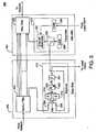
- FIG. 2depicts exemplary, coherent-receiver based OADM 200 according to a preferred embodiment of the present invention.
- OADM 200includes drop side 202 and add side 204.
- the drop sideincludes splitter 206, wavelength blocker 208, and coherent receiver 210, which can either be implemented in a balanced configuration (illustrated) or in a single-ended configuration (not illustrated).
- the add sideincludes transmitter 212 and coupler 214.
- the drop-leg multiplexfeeds input 234 of coupler 236.
- the other input (238) of coupler 236is fed by one output of splitter 232 of transmitter 212 from the add side of the OADM.
- splitter 232is fed by laser 228, which has been tuned to emit an optical signal centered at wavelength ⁇ d .
- i1 ⁇ N and some of the power from the laser signal of wavelength ⁇ d beat against each other upon photodetection at photodiodes 216 and 218, respectively, resulting in a heterodyning (if the beat frequency is not at baseband) or homodyning (if the beat frequency is at baseband) of the signal of interest s d ( ⁇ d ) .
- a phase-diversity coherent receivercan be used to coherently detect the dropped signal.
- the electrical signalis then further processed (e.g., differenced ( 220 ) in the case of a balanced setup, squared and added in case of a phase-diversity setup, demodulated to baseband in a heterodyne setup, or simply low-pass filtered and amplified in case of a homodyne setup) by appropriate signal processing electronics 222.
- the processed signalis then fed to sampling/decision circuit 224 for detection and recovery of the data that was modulated onto s d ( ⁇ d ).
- the recovered datais then "dropped" to the local client.
- Wavelength blocker 208which receives a copy of the wavelength multiplex on the "pass leg" out of splitter 206, is configured to block the dropped wavelength ⁇ d associated with the dropped signal element s d ( ⁇ d ) and pass the rest of the elements S d ( ⁇ i )
- i1 ...N, i ⁇ d in the multiplex to the add side of the OADM.
- optical transmitter 212is configured to modulate a locally supplied data stream onto an optical carrier of the same wavelength ⁇ d that was dropped from the drop side of the OADM.
- This modulated optical carrier s a ( ⁇ d ) from the transmitteris then combined with the wavelengths of the multiplex that were passed from the drop side to the add side of the OADM to form a new multiplexed signal S a ( ⁇ i )
- i1 ⁇ N that is output from the OADM.
- the transmitteris also configured to supply light of wavelength ⁇ d to the receiver of drop side 202.
- laser 228is tuned to a wavelength ⁇ d , and its output is fed to splitter 232.
- One output of splitter 232feeds input 238 of coupler 236 of receiver 210.
- the other outputfeeds external modulator (e.g., Mach-Zehnder modulator) 230 where the laser output at wavelength ⁇ d is modulated with data from the local client that may have been pre-coded (e.g., return-to-zero (RZ) coded) by coder 226 .
- external modulatore.g., Mach-Zehnder modulator
- This modulated add-side component signal s a ( ⁇ d )is then fed to coupler 214 where it is combined with the elements S d ( ⁇ i )
- i1...N, i ⁇ d of the input multiplex that were passed to the coupler by drop side 202 , and the resulting combined multiplex is then output from the OADM.
- FIG. 3illustrates an alternative embodiment 300 of the optical device of the present invention.
- Components of this embodimentoperate similarly to corresponding components of the embodiment of FIG. 2.
- the splitter and wavelength blocker of FIG. 2have been replaced with demultiplexing filter 302, and coupler 214 of FIG. 2 has been replaced with a multiplexing filter 304.
- the demux filterproduces N output channels, each of a single wavelength.
- One of these wavelengthsfeeds receiver 210 where it is processed as described before with respect to the embodiment of FIG. 2.
- the remaining outputs, as well as the optical signal output from transmitter 212,feed mux filter 304, which combines the signals to form the overall output of the device.
- the receivers described in FIGs. 2 and 3can be heterodyne, homodyne, or "phase-diversity coherent" homodyne receiver; in the latter, the local laser is not necessarily phase-aligned or phase-synchronized with the incoming signal, but the signal is essentially demodulated to baseband by the optical beating process.
- special circuitryis added to a receiver to align the LO to the phase of the received carrier. This alignment is useful in systems that employ certain modulation schemes (e.g., phase-shift-keyed modulation) since the local oscillator may be used as a reference against which changes in the phase of the received signal (e.g., due to phase modulation) can be measured.
- the output of splitter 232may be passed through a phase adjuster before being fed to coupler 236.
- the phase of the lasermay be adjusted so that it is aligned with the phase of the incoming signal S d ( ⁇ d ) to support true homodyne reception.
- the phase of laser 228maybe adjusted directly, as would be understood to one skilled in the art.
- the wavelength blocked by wavelength blocker 208 and the fundamental wavelength emitted by laser 228are configurable and may be configured dynamically (e.g., via a controller with simple network management protocol support).
- exemplary OADM embodiment 200 of FIG. 2may be used to demodulate an amplitude-modulated (e.g., on-off keyed (OOK)) optical signal, as well as other modulation formats (e.g., carrier-suppressed OOK, duobinary, alternate mark inversion, chirped return-to-zero, differential phase-shift-keyed (DPSK), and differential quadrature-phase-shift-keying (DPQSK)) as would be understood by one skilled in the art.
- OOKon-off keyed
- DPSKdifferential phase-shift-keyed
- DPQSKdifferential quadrature-phase-shift-keying
- the coherent receiver 210 as described in the exemplary embodiment of FIG. 2includes circuitry for the conversion of the homodyned optical signal to an electrical format
- a device that includes a mechanism that transmits the combined local oscillator signal and the received signal and drops the combined signal to the local client or a remote location without first converting it into the electrical domain and homodyningis contemplated in the present invention.
- a device that includes a receiver that homodynes the received optical signal with a portion of the light that is used by the transmitter, and then performs O-E conversion as per the discussion corresponding to receiver 210 of FIG. 2, but then performs an E-O conversion prior to dropping the signal to the local client or prior to processing the signal further in the optical domainis also contemplated in the present invention.
- the present inventionwas described with respect to a device known in the art as an OADM and with respect to a single drop and a single add wavelength, the concepts and advantages of the present invention also apply to a broad range of optical devices and subsystems where both a receiver and transmitter are present and one or more of the laser or laser sources in the device may be shared with the receiver electronics. It also applies to devices that receive, block, and/or transmit more than one concurrent wavelength, as would be understood to one skilled in the art. The present invention also applies to an end node of an optical communications system where more than one of the incoming data signals corresponding to wavelengths in the input WDM signal is dumped (i.e., not passed along together with the locally added light).
- elements of the present inventionmay be implemented by various techniques and in various technologies while remaining within the principle and scope of the present invention.
- These techniques and technologiesinclude, but are not limited to: photonic integrated receiver technology, integrated optics (including silicon on silicon substrate or Si:SiO 2 ), fiber optics, free-space optics, thin film, InGaAs, micromirror micro-electromechanical arrays, and optical grating subsystems.
Landscapes
- Engineering & Computer Science (AREA)
- Computer Networks & Wireless Communication (AREA)
- Signal Processing (AREA)
- Physics & Mathematics (AREA)
- Electromagnetism (AREA)
- Optical Communication System (AREA)
Description
- The present invention relates generally to the field of optical telecommunications, and, more specifically, to optical devices such as optical add/drop multiplexers (OADMs).
- In state-of-the-art, optical wavelength-division-multiplexed (WDM) communication systems, multiple, individually-data-modulated wavelengths of light are multiplexed into an optical fiber and routed to a remote location via ring or mesh optical networks. Along the path from source to destination, optical devices, such as OADMs, are commonly employed to modify the contents, and in some cases the quality, of the multiplex. Such modification includes grooming the multiplex by adding, dropping, replacing, and/or frequency-translating data-carrying wavelengths of light within the multiplex.
- At the input or "drop" side of an OADM, an input WDM signal is typically split (e.g., using a power splitter) into a pass leg and a drop leg. The drop leg typically feeds a receiver that is configured to receive, detect, and demodulate one of the data-modulated wavelengths λd of the input multiplex. The pass leg is typically fed to a wavelength blocker that is configured to block the dropped wavelength λd, and pass the rest of the wavelengths in the multiplex to the "add" side of the OADM. Alternatively, the functionality of power splitting and wavelength blocking can be integrated into a WDM demultiplexing filter.
- At the add side of the OADM, an optical transmitter is configured to modulate a locally supplied data stream onto an optical carrier of the same wavelength λd that was dropped from the drop side of the OADM. This modulated wavelength from the transmitter is then combined with the wavelengths of the multiplex that were passed to the add side from the drop side to form a new multiplex that is output from the OADM.
- The transmitter in the OADM is commonly of the externally modulated laser variety. Such a transmitter includes a fixed-wavelength or a tunable laser coupled to a modulator (e.g., a Mach-Zehnder modulator) whose modulation is controlled by a properly coded version of the locally supplied data stream.
- The receiver is typically of the direct-detection variety. Such receivers generally include a pin-type or avalanche-type photodiode coupled to an amplifier, filtering electronics, and a sampling/decision circuit.
- A Technical Report, dated May 2002, from the University of Kansas, by C. T. Allen and Y. Cobanoglu, in Fig. 6.2-1, discloses a communication system having a transmitter and a receiver coupled via a free-space transmission link having transmit and receive telescopes. The system has a laser, the output of which is split into two beams directed to the transmitter and receiver, respectively. At the transmitter, the first beam is modulated with data, amplified, and applied to the transmit telescope for transmission to the receiver. At the receiver, the transmitted beam is received via the receive telescope and, together with the second beam, which serves as a local oscillator, applied to a homodyne detector for data processing and recovery. Thus, in the communication system disclosed in this report, the incoming signal (received via the receive telescope) is based on the outgoing signal (transmitted via the transmit telescope).
- U.S. Patent No. 5,438,445 discloses an optical wavelength multiplexing add/drop apparatus. The apparatus has a first optical coupler that splits a received optical wavelength multiplex signal into multiple (attenuated) copies. Some of the copies are applied to the corresponding coherent optical demodulators to extract data, and one copy is amplified and applied to a second optical coupler. The extracted data are then applied to one or more laser sources to produce optical signals that have wavelengths different from those present in the input multiplex signal. The second optical coupler then combines the amplified copy with the signals generated by the laser source(s) and outputs the combined signal from the apparatus. As a result, the output signal has all of the components of the initial (received) multiplex signal plus the components generated by the laser sources, wherein some of the components differ only in wavelength while carrying the same data. Since different components of the output signal can be independently routed, the apparatus disclosed in this patent enables simultaneous transmission of the same data to multiple destinations.
- European Patent Application EP-A2-0 222 384 discloses a bidirectional optical communication system including an optical combiner functioning as a combiner in which receiving signal light and local oscillator light are combined to produce intermediate frequency signal and as a divider in which the receiving signal light and transmitting signal light are divided so that parts to be used are decreased in number thereby decreasing the manufacturing costs and volume thereof.
- A method and apparatus according to the present invention are set out in the independent claims, to which the reader is now referred. Preferred features are laid out in the dependent claims.
- According to one embodiment, problems in the prior art are addressed in accordance with principles of the present invention by providing an optical device, such as an optical add/drop multiplexer (OADM), having an add-side laser that provides not only a source for an add-side wavelength to be added to an output of the device, but also a reference for a receive-side local oscillator in a coherent receiver that is included in the optical device. Thus, instead of having a separate local oscillator (LO) in the front end of the coherent receiver in the receive-side of the optical device, optical devices of the present invention use the optical signal generated by the add-side laser to provide a mixing frequency for the coherent receiver in either a heterodyne or a homodyne configuration.
- In one embodiment, the present invention is an apparatus that includes: (1) a splitter adapted to split an incoming optical signal received by the apparatus into at least first and second portions; (2) an optical receiver adapted to process at least the first portion of the incoming optical signal; and (3) an optical transmitter adapted to generate at least a portion of an outgoing optical signal transmitted by the apparatus, wherein: (i) the optical transmitter comprises a light generator adapted to generate light for the portion of the outgoing optical signal generated by the optical transmitter; (ii) the optical receiver is optically coupled to the light generator to receive and use part of the light generated by the light generator to process the first portion of the incoming optical signal; (iii) the outgoing optical signal is based on the incoming optical signal; and (iv) at least one optical component of the incoming optical signal is prevented from going into the outgoing optical signal, wherein the prevented component is present in the first portion and has a wavelength that is at least one of the wavelengths in the light generated by the light generator.
- In another embodiment, the present invention is a method for processing WDM optical signals in an optical device, comprising: (1) splitting an incoming WDM optical signal received by the optical device into first and second parts; (2) dropping a first optical signal from the first part of the incoming WDM optical signal at a receiver; (3) generating light for a second optical signal; and (4) adding the second optical signal to the second part of the incoming WDM optical signal to generate an outgoing WDM optical signal transmitted by the optical device, wherein: (i) the optical receiver is adapted to receive and use part of the light generated for the second optical signal to process the first optical signal; and (ii) the method includes the step of preventing the first optical signal from being included the outgoing WDM optical signal, wherein the first and second optical signals have substantially the same fundamental carrier wavelengths.
- Other aspects, features, and advantages of the present invention will become more fully apparent from the following detailed description, the appended claims, and the accompanying drawings in which:
- FIG. 1 depicts exemplary optical add/drop multiplexer (OADM)100 according to the prior art.
- FIG. 2 depicts exemplary coherent-receiver-based OADM200 according to a preferred embodiment of the present invention.
- FIG. 3 depicts another exemplary coherent-receiver-based
optical device 300 according to the present invention. - Reference herein to "one embodiment" or "an embodiment" means that a particular feature, structure, or characteristic described in connection with the embodiment can be included in at least one embodiment of the invention. The appearances of the phrase "in one embodiment" in various places in the specification are not necessarily all referring to the same embodiment, nor are separate or alternative embodiments mutually exclusive of other embodiments.
- FIG.1 depicts exemplary OADM100 according to the prior art. As shown, OADM100 includes
drop side 102 and addside 104. The drop side includessplitter 106,wavelength blocker 108, andreceiver 110. The add side includestransmitter 112 andcoupler 114. - At
drop side 102 of the OADM, an input multiplex of data-encoded optical signalsSd(λi)|i=1···N is received from a network and split usingpower splitter 106 into a drop leg that feedsreceiver 110 and a pass leg that feedswavelength blocker 108. Atreceiver 110, one of the constituent elements (e.g.,sd (λd)), a "drop wavelength" component of the drop-leg multiplex signal is selected from the multiplex by demultiplexer-selector 116 and that element is passed tophotodiode 118 where it is converted from an optical signal to an electrical signal. The electrical output of the photodiode is then amplified bypreamplifier 120 and filtered by low-pass filter 122. The output of the low-pass filter is passed to sampling/decision circuit 124 for detection and recovery of the data that was modulated ontosd (λd) by an entity upstream of the OADM. The recovered data is then "dropped" to the local client.Wavelength blocker 108, which receives a copy of the wavelength multiplex on the "pass leg" out ofsplitter 106, is configured to block the dropped wavelengthλd associated with the dropped signal elementSd(λd) and pass the rest of the elementsSd(λi)|i=1...N, i≠d in the multiplex to the add side of the OADM. Alternatively, in place ofcolorless splitter 106, demux select116 andwavelength blocker 108 on the add side, and coupler114 on the drop side, state-of-the art implementations ofOADMs might use, without change in functionality, a wavelength-selective drop filter on the add side, and a wavelength-selective add filter on the drop side. This alternative arrangement has the advantage of reduced insertion losses. - At add
side 104 of the OADM,optical transmitter 112 is configured to modulate a locally supplied data stream onto an optical carrier of the same wavelength λd that was dropped from the drop side of the OADM. This modulated optical carriersa(λd) from the transmitter is then combined incoupler 114 with the wavelengths of the multiplex that were passed from the drop side to the add side of the OADM to form a new multiplexed signalSa(λi)|i=1...N that is output from the OADM. - Specifically, in the exemplary externally modulated
transmitter configuration 112 depicted inFIG. 1,laser 128 is tuned to a wavelengthλd, and its output is fed to external modulator (e.g., Mach-Zehnder modulator)130 where the laser output at wavelength λd is modulated with data from the local client that might have been pre-coded (e.g., return-to-zero (RZ) coded) bycoder 126. This modulated add-side component signalsa(λd) is then fed tocoupler 114 where it is combined with the elements of the input multiplexSd(λi)|i=1...N,i≠d that were passed to the coupler bydrop side 102, and the resulting complete multiplex is then output from the OADM. - Note that, as is common in the prior art,
receiver 110 is of the direct-detection variety. However, recently, there has been interest in the use of coherent receivers, especially for free-space optical applications. Such receivers typically make use of a local oscillator (LO) in their front end to provide a mixing frequency in either a heterodyne or a homodyne configuration. - FIG. 2 depicts exemplary, coherent-receiver based
OADM 200 according to a preferred embodiment of the present invention. - As shown,
OADM 200 includesdrop side 202 and addside 204. The drop side includessplitter 206,wavelength blocker 208, andcoherent receiver 210, which can either be implemented in a balanced configuration (illustrated) or in a single-ended configuration (not illustrated). The add side includestransmitter 212 andcoupler 214. - At
drop side 202 of the OADM, an input multiplex of data-encoded optical signalsSd(λi)|i=1···N is split usingpower splitter 206 into a drop leg that feedsreceiver 210 and a pass leg that feedswavelength blocker 208. - At
receiver 210, the drop-leg multiplex feedsinput 234 ofcoupler 236. The other input(238) ofcoupler 236 is fed by one output ofsplitter 232 oftransmitter 212 from the add side of the OADM. Note thatsplitter 232 is fed bylaser 228, which has been tuned to emit an optical signal centered at wavelength λd. Thus, incoupler 236, the received signalSd(λi)|i=1···N and some of the power from the laser signal of wavelength λd beat against each other upon photodetection atphotodiodes signal processing electronics 222. The processed signal is then fed to sampling/decision circuit 224 for detection and recovery of the data that was modulated ontosd(λd). The recovered data is then "dropped" to the local client. Wavelength blocker 208, which receives a copy of the wavelength multiplex on the "pass leg" out ofsplitter 206, is configured to block the dropped wavelength λd associated with the dropped signal elementsd(λd) and pass the rest of the elementsSd(λi)|i=1...N, i≠d in the multiplex to the add side of the OADM.- At add
side 204 of the OADM,optical transmitter 212 is configured to modulate a locally supplied data stream onto an optical carrier of the same wavelength λd that was dropped from the drop side of the OADM. This modulated optical carriersa(λd) from the transmitter is then combined with the wavelengths of the multiplex that were passed from the drop side to the add side of the OADM to form a new multiplexed signalSa(λi)|i=1···N that is output from the OADM. The transmitter is also configured to supply light of wavelengthλd to the receiver ofdrop side 202. - More specifically, in the exemplary externally modulated
transmitter configuration 212 depicted inFIG. 2,laser 228 is tuned to a wavelengthλd, and its output is fed tosplitter 232. One output ofsplitter 232 feedsinput 238 ofcoupler 236 ofreceiver 210. The other output feeds external modulator (e.g., Mach-Zehnder modulator)230 where the laser output at wavelength λd is modulated with data from the local client that may have been pre-coded (e.g., return-to-zero (RZ) coded) bycoder 226. This modulated add-side component signalsa(λd) is then fed tocoupler 214 where it is combined with the elementsSd(λi)|i=1...N, i≠d of the input multiplex that were passed to the coupler bydrop side 202, and the resulting combined multiplex is then output from the OADM. - FIG. 3 illustrates an
alternative embodiment 300 of the optical device of the present invention. Components of this embodiment operate similarly to corresponding components of the embodiment ofFIG. 2. However, in the embodiment ofFIG. 3, the splitter and wavelength blocker ofFIG. 2 have been replaced withdemultiplexing filter 302, andcoupler 214 ofFIG. 2 has been replaced with amultiplexing filter 304. The demux filter produces N output channels, each of a single wavelength. One of these wavelengths feedsreceiver 210 where it is processed as described before with respect to the embodiment ofFIG. 2. The remaining outputs, as well as the optical signal output fromtransmitter 212, feedmux filter 304, which combines the signals to form the overall output of the device. - Note that the receivers described inFIGs. 2 and3 can be heterodyne, homodyne, or "phase-diversity coherent" homodyne receiver; in the latter, the local laser is not necessarily phase-aligned or phase-synchronized with the incoming signal, but the signal is essentially demodulated to baseband by the optical beating process. In a strictly homodyne receiver, special circuitry is added to a receiver to align the LO to the phase of the received carrier. This alignment is useful in systems that employ certain modulation schemes (e.g., phase-shift-keyed modulation) since the local oscillator may be used as a reference against which changes in the phase of the received signal (e.g., due to phase modulation) can be measured. In an alternative embodiment of the present invention, the output of
splitter 232 may be passed through a phase adjuster before being fed tocoupler 236. In the phase adjuster, the phase of the laser may be adjusted so that it is aligned with the phase of the incoming signalSd(λd) to support true homodyne reception. Alternatively, the phase oflaser 228 maybe adjusted directly, as would be understood to one skilled in the art. - Note that, although not explicitly shown inFIG. 2, in one or more implementations of the present invention, the wavelength blocked by
wavelength blocker 208 and the fundamental wavelength emitted bylaser 228 are configurable and may be configured dynamically (e.g., via a controller with simple network management protocol support). - Note that, the invention as described with respect to
exemplary OADM embodiment 200 ofFIG. 2 may be used to demodulate an amplitude-modulated (e.g., on-off keyed (OOK)) optical signal, as well as other modulation formats (e.g., carrier-suppressed OOK, duobinary, alternate mark inversion, chirped return-to-zero, differential phase-shift-keyed (DPSK), and differential quadrature-phase-shift-keying (DPQSK)) as would be understood by one skilled in the art. - Although the
coherent receiver 210 as described in the exemplary embodiment ofFIG. 2 includes circuitry for the conversion of the homodyned optical signal to an electrical format, a device that includes a mechanism that transmits the combined local oscillator signal and the received signal and drops the combined signal to the local client or a remote location without first converting it into the electrical domain and homodyning is contemplated in the present invention. Likewise, a device that includes a receiver that homodynes the received optical signal with a portion of the light that is used by the transmitter, and then performs O-E conversion as per the discussion corresponding toreceiver 210 ofFIG. 2, but then performs an E-O conversion prior to dropping the signal to the local client or prior to processing the signal further in the optical domain, is also contemplated in the present invention. - Although the present invention was illustrated with respect to a preferred embodiment that includes a balanced receiver, as discussed, single-ended, homodyne, heterodyne, or phase-diversity homodyne receiver configurations are within the scope of the present invention.
- Although the present invention was described with respect to a device known in the art as an OADM and with respect to a single drop and a single add wavelength, the concepts and advantages of the present invention also apply to a broad range of optical devices and subsystems where both a receiver and transmitter are present and one or more of the laser or laser sources in the device may be shared with the receiver electronics. It also applies to devices that receive, block, and/or transmit more than one concurrent wavelength, as would be understood to one skilled in the art. The present invention also applies to an end node of an optical communications system where more than one of the incoming data signals corresponding to wavelengths in the input WDM signal is dumped (i.e., not passed along together with the locally added light).
- Note that elements of the present invention may be implemented by various techniques and in various technologies while remaining within the principle and scope of the present invention. These techniques and technologies include, but are not limited to: photonic integrated receiver technology, integrated optics (including silicon on silicon substrate or Si:SiO2), fiber optics, free-space optics, thin film, InGaAs, micromirror micro-electromechanical arrays, and optical grating subsystems.
- While this invention has been described with reference to illustrative embodiments, this description should not be construed in a limiting sense. Various modifications of the described embodiments, as well as other embodiments of the invention, which are apparent to persons skilled in the art to which the invention pertains, are deemed to lie within the principle and scope of the invention as expressed in the following claims.
Claims (10)
- An optical device, comprising:means for splitting (206, 208, 302) adapted to split an incoming optical signal received by the optical device into at least first and second portions;an optical receiver (210) adapted to process at least the first portion of the incoming optical signal; andan optical transmitter (212) adapted to generate at least a portion of an outgoing optical signal transmitted by the optical device, wherein:the optical transmitter comprises a light generator (228) adapted to generate light for the portion of the outgoing optical signal generated by the optical transmitter;the optical receiver is optically coupled to the light generator to receive and use part of the light generated by the light generator to process the first portion of the incoming optical signal; andthe optical device isCHARACTERISED in that:the outgoing optical signal is based on the incoming optical signal;the means for splitting is adapted to prevent at least one optical component of the incoming optical signal from going into the outgoing optical signal, wherein the prevented component is present in the first portion and has a carrier wavelength that is at least one of the wavelengths in the light generated by the light generator; andthe optical transmitter is adapted to generate a component of the outgoing optical signal having said carrier wavelength.
- The optical device of claim 1, wherein:the means for splitting comprises a power splitter (206) and a wavelength blocker (208), wherein:the power splitter (206) is adapted to produce first and second attenuated copies of the incoming optical signal, wherein the first attenuated copy serves as the first portion applied to the optical receiver, and to apply the second attenuated copy to the wavelength blocker (208); andthe wavelength blocker (208) is adapted to:receive the second attenuated copy from the power splitter,block the at least one optical component from the second attenuated copy, andpass the remainder of the second attenuated copy, wherein the passed remainder serves as the second portion; andthe optimal device further comprises a coupler (214) adapted to combine the remainder passed by the wavelength blocker with the portion of the outgoing optical signal generated by the transmitter.
- The optical device of claim 1, wherein the means for splitting is a demux filter (302) adapted to wavelength split the incoming optical signal into N discrete single wavelength signals, wherein:the receiver receives one of the N single wavelength signals; andan output mux filter (304) receives the rest of the N single wavelength signals and combines them with the portion of the outgoing optical signal generated by the transmitter.
- The optical device of claim 1, wherein the light generator is a laser (228) that is adapted to be dynamically tuned to one wavelength of a plurality of different wavelengths.
- A method for processing WDM optical signals in an optical device, comprising:splitting an incoming WDM optical signal received by the optical device into first and second parts;dropping a first optical signal from the first part of the incoming WDM optical signal at a receiver;generating light for a second optical signal; andadding the second optical signal to the second part of the incoming WDM optical signal to generate an outgoing WDM optical signal transmitted by the optical device, wherein:the optical receiver is adapted to receive and use part of the light generated for the second optical signal to process the first optical signal; andthe method isCHARACTERISED by preventing the first optical signal from being included in the outgoing WDM optical signal, wherein the first and second optical signals have substantially the same fundamental carrier wavelengths.
- The optical device of claim 1, wherein the optical device is an optical add/drop multiplexer (200) and the incoming and outgoing optical signals are WDM signals.
- The optical device of claim 1, wherein the optical device is an end node of an optical communications system and the incoming optical signal is a WDM signal.
- The optical device of claim 1, wherein the receiver is a homodyne receiver or a phase-diversity homodyne receiver.
- The optical device of claim 1, wherein the receiver comprises an optical coupler (236) having first (234) and second (238) input ports and a first output port, wherein:the first input port is adapted to receive a first signal that includes the portion of the incoming optical signal received by the optical device; andthe second port is adapted to receive a second signal that includes the part of the light generated by the light generator; wherein:the coupler optically couples the first and second signals and outputs the result of the coupling on the first output port, and the receiver further comprises circuitry (216-224) adapted to convert and process the result of the coupling that is output from the first output port of the coupler to and in the electrical domain.
- The method of claim 5, comprising:wavelength demultiplexing the incoming WDM optical signal into N single wavelength signals,receiving one of the single wavelength signals of a first wavelength at the receiver;sending the N-1 remaining single wavelength signals to an output multiplexer;generating light of substantially the first wavelength;feeding the light of substantially the first wavelength to the receiver, and to a transmitter that produces an added optical signal of substantially the first wavelength; andcombining, at the multiplexer, the added optical signal and the N-1 remaining single wavelength signals to form the outgoing WDM optical signal.
Applications Claiming Priority (2)
| Application Number | Priority Date | Filing Date | Title |
|---|---|---|---|
| US615701 | 2003-07-09 | ||
| US10/615,701US7269356B2 (en) | 2003-07-09 | 2003-07-09 | Optical device with tunable coherent receiver |
Publications (2)
| Publication Number | Publication Date |
|---|---|
| EP1496636A1 EP1496636A1 (en) | 2005-01-12 |
| EP1496636B1true EP1496636B1 (en) | 2006-10-18 |
Family
ID=33452666
Family Applications (1)
| Application Number | Title | Priority Date | Filing Date |
|---|---|---|---|
| EP04253965AExpired - LifetimeEP1496636B1 (en) | 2003-07-09 | 2004-07-01 | Optical device with tunable coherent receiver |
Country Status (5)
| Country | Link |
|---|---|
| US (1) | US7269356B2 (en) |
| EP (1) | EP1496636B1 (en) |
| JP (1) | JP4841121B2 (en) |
| CN (1) | CN100437177C (en) |
| DE (1) | DE602004002811T2 (en) |
Families Citing this family (46)
| Publication number | Priority date | Publication date | Assignee | Title |
|---|---|---|---|---|
| JP4530821B2 (en)* | 2004-08-16 | 2010-08-25 | 富士通株式会社 | Optical add / drop device |
| US7742701B2 (en)* | 2005-03-16 | 2010-06-22 | Michael George Taylor | Coherent optical channel substitution |
| US7826752B1 (en)* | 2005-06-02 | 2010-11-02 | Level 3 Communications, Llc | Optical transmission apparatuses, methods, and systems |
| FR2901078B1 (en)* | 2006-05-11 | 2008-07-04 | Alcatel Sa | RECONFIGURABLE INSERTION / EXTRACTION OPTICAL MULTIPLEXING DEVICE HAVING OPTICAL INPUT / OUTPUT INTERFACES WITH BROADBANDS |
| ES2326152B1 (en)* | 2006-12-29 | 2010-06-29 | Universitat Politecnica De Catalunya (Upc) | HOMODINE RECEIVER FOR OPTICAL COMMUNICATIONS WITH PROCESSING AFTER. |
| WO2010043035A1 (en)* | 2008-10-17 | 2010-04-22 | Nortel Networks Limited | Coherent augmented optical add-drop multiplexer |
| US8433192B2 (en)* | 2008-12-08 | 2013-04-30 | Ciena Corporation | Dynamic performance monitoring systems and methods for optical networks |
| US9490894B2 (en)* | 2008-12-08 | 2016-11-08 | Ciena Corporation | Coherent probe and optical service channel systems and methods for optical networks |
| CN102067484B (en)* | 2008-12-08 | 2015-11-25 | 骁阳网络有限公司 | The method of the data processing in optical-fiber network and optical-fiber network parts and communication system |
| US20100158521A1 (en) | 2008-12-18 | 2010-06-24 | Alcatel-Lucent Usa Inc. | Optical mixer for coherent detection of polarization-multiplexed signals |
| MY167202A (en) | 2009-03-20 | 2018-08-13 | Alcatel Lucent | Coherent optical detector having a multifunctional waveguide grating |
| EP2433378B1 (en)* | 2009-05-20 | 2019-06-19 | NeoPhotonics Corporation | 40,50 and 100 gb/s optical transceivers/transponders in 300pin and cfp msa modules |
| US8275224B2 (en)* | 2009-08-14 | 2012-09-25 | Alcatel Lucent | Coherent receiver having an interleave-chirped arrayed waveguide grating |
| WO2011044371A1 (en)* | 2009-10-09 | 2011-04-14 | Nec Laboratories America, Inc. | Transponder aggregator without wavelength selector colorless and directionless multi-degree roadm node |
| US8526831B2 (en)* | 2009-12-18 | 2013-09-03 | Alcatel Lucent | Receiver algorithms for coherent detection of polarization-multiplexed optical signals |
| US8295714B2 (en)* | 2009-12-18 | 2012-10-23 | Alcatel Lucent | Receiver algorithms for coherent detection of polarization-multiplexed optical signals |
| US8571423B2 (en)* | 2009-12-18 | 2013-10-29 | Alcatel Lucent | Receiver algorithms for coherent detection of polarization-multiplexed optical signals |
| DE102010004285A1 (en)* | 2010-01-11 | 2011-07-14 | Fraunhofer-Gesellschaft zur Förderung der angewandten Forschung e.V., 80686 | network element |
| JP5636684B2 (en)* | 2010-01-29 | 2014-12-10 | 富士通株式会社 | Coherent optical communication device and coherent optical communication method |
| US10461880B2 (en) | 2010-08-26 | 2019-10-29 | Ciena Corporation | Flexible grid optical spectrum transmitter, receiver, and transceiver |
| US9197354B2 (en) | 2010-08-26 | 2015-11-24 | Ciena Corporation | Concatenated optical spectrum transmission systems and methods |
| US8913899B2 (en)* | 2010-12-07 | 2014-12-16 | Alcatel Lucent | Distribution of optical power in an optical transport system |
| US20120269514A1 (en)* | 2011-04-25 | 2012-10-25 | Fujitsu Limited | High Speed IO with Coherent Detection |
| US20120288286A1 (en)* | 2011-05-12 | 2012-11-15 | Alcatel-Lucent Usa Inc. | Optical receiver for amplitude-modulated signals |
| CN102957477B (en)* | 2011-08-30 | 2015-12-09 | 华为技术有限公司 | Signal detecting method and optical signal reception system |
| WO2013140769A1 (en)* | 2012-03-21 | 2013-09-26 | 日本電気株式会社 | Direct-current offset control circuit, optical receiver, optical node device, and method for controlling optical receiver |
| EP2693671A1 (en)* | 2012-07-30 | 2014-02-05 | Alcatel Lucent | Method and related apparatus for coherent optical transmission |
| JP6065101B2 (en) | 2013-03-15 | 2017-01-25 | 日本電気株式会社 | Duplexer |
| US9584220B2 (en)* | 2013-03-15 | 2017-02-28 | Nec Corporation | Optical transmission/reception device, optical communication system and optical transmission/reception method |
| CN107466448B (en)* | 2015-04-09 | 2020-10-09 | 华为技术有限公司 | Method implemented in an optical transceiver node and optical transceiver node |
| US9571200B2 (en) | 2015-07-09 | 2017-02-14 | Elenion Technologies, Llc | Transmitter optical signal to noise ratio improvement through receiver amplification in single laser coherent systems |
| US20170126352A1 (en)* | 2015-11-02 | 2017-05-04 | Alcatel-Lucent Usa, Inc. | Optical modem |
| US10243722B2 (en)* | 2016-11-22 | 2019-03-26 | Huawei Technologies Co., Ltd. | Optical interconnecting network architecture |
| US10079643B2 (en)* | 2016-11-23 | 2018-09-18 | Stmicroelectronics (Research & Development) Limited | Devices and methods for transmitting and receiving in an optical communications system |
| US10917172B2 (en)* | 2017-07-14 | 2021-02-09 | Nec Corporation | Pluggable optical module, optical communication system, and control method of pluggable optical module |
| EP3688422B1 (en) | 2017-09-29 | 2024-05-15 | Apple Inc. | Connected epitaxial optical sensing systems |
| US12066702B1 (en) | 2018-09-25 | 2024-08-20 | Apple Inc. | Systems and methods for distinguishing between a user and an object |
| US11857298B1 (en) | 2019-09-06 | 2024-01-02 | Apple Inc. | Devices having matter differentiation detectors |
| CN110661570B (en)* | 2019-09-29 | 2023-04-11 | 长春理工大学 | Space laser communication system |
| US12206222B2 (en) | 2020-08-20 | 2025-01-21 | Apple Inc. | Integrated edge-generated vertical emission laser |
| US12089931B1 (en) | 2020-09-11 | 2024-09-17 | Apple Inc. | Optical sensor for skin-contact detection and physiological parameter measurement at wearable electronic device |
| US12204289B1 (en) | 2020-09-11 | 2025-01-21 | Apple Inc. | Device removal indication using different object proximity thresholds |
| US12164027B1 (en) | 2020-09-14 | 2024-12-10 | Apple Inc. | Multi-pathway distance measurements for optical sensors |
| US12372724B2 (en) | 2020-09-23 | 2025-07-29 | Apple Inc. | Light splitting device |
| US11815719B2 (en)* | 2020-09-25 | 2023-11-14 | Apple Inc. | Wavelength agile multiplexing |
| CN116087965A (en)* | 2023-04-06 | 2023-05-09 | 天津大学合肥创新发展研究院 | All-solid-state frequency modulation continuous wave laser radar system based on optical phased array technology |
Family Cites Families (8)
| Publication number | Priority date | Publication date | Assignee | Title |
|---|---|---|---|---|
| DE3827228A1 (en)* | 1988-08-11 | 1990-02-15 | Standard Elektrik Lorenz Ag | TRANSMITTER / RECEIVER FOR A BIDIRECTIONAL COHERENT-OPTICAL TRANSMISSION SYSTEM |
| JP3117018B2 (en) | 1990-10-29 | 2000-12-11 | 株式会社日立製作所 | Network equipment |
| US5438973A (en)* | 1993-10-08 | 1995-08-08 | Crystal Systems, Inc. | Shaped blades |
| US6078418A (en)* | 1997-08-12 | 2000-06-20 | Lucent Technologies Inc. | Wavelength locking of variable dispersive elements |
| KR20010034668A (en)* | 1998-03-24 | 2001-04-25 | 오카야마 노리오 | WDM transmission repeater, WDM transmission system and WDM transmission method |
| KR100295810B1 (en)* | 1998-06-02 | 2001-10-26 | 서평원 | Wavelength Division Multiplexing Optical Network Channel Monitoring System |
| KR100400362B1 (en)* | 1998-08-04 | 2003-11-14 | 삼성전자주식회사 | Apparatus for optical add drop multiplexing and WDM optical network comprising it |
| US6661973B1 (en)* | 1999-06-04 | 2003-12-09 | David R. Huber | Optical transmission systems, apparatuses, and methods |
- 2003
- 2003-07-09USUS10/615,701patent/US7269356B2/ennot_activeExpired - Lifetime
- 2004
- 2004-07-01EPEP04253965Apatent/EP1496636B1/ennot_activeExpired - Lifetime
- 2004-07-01DEDE602004002811Tpatent/DE602004002811T2/ennot_activeExpired - Lifetime
- 2004-07-08CNCNB2004100633369Apatent/CN100437177C/ennot_activeExpired - Fee Related
- 2004-07-09JPJP2004202608Apatent/JP4841121B2/ennot_activeExpired - Fee Related
Also Published As
| Publication number | Publication date |
|---|---|
| DE602004002811T2 (en) | 2007-08-23 |
| EP1496636A1 (en) | 2005-01-12 |
| DE602004002811D1 (en) | 2006-11-30 |
| CN1576922A (en) | 2005-02-09 |
| US7269356B2 (en) | 2007-09-11 |
| US20050008369A1 (en) | 2005-01-13 |
| CN100437177C (en) | 2008-11-26 |
| JP2005045789A (en) | 2005-02-17 |
| JP4841121B2 (en) | 2011-12-21 |
Similar Documents
| Publication | Publication Date | Title |
|---|---|---|
| EP1496636B1 (en) | Optical device with tunable coherent receiver | |
| US10944482B2 (en) | Coherent optical receiver | |
| US7526211B2 (en) | Frequency agile transmitter and receiver architecture for DWDM systems | |
| CA2075387C (en) | Low distortion laser system for am fiber optic communication | |
| US20090136229A1 (en) | Method and System for Transmitting Information in an Optical Communication System Using Distributed Amplification | |
| KR20190127783A (en) | Optical communication system, apparatus and method including high performance optical receiver | |
| EP1393492A1 (en) | Method and system for communicating a clock signal over an optical link | |
| EP1548967B1 (en) | Method and system for demultiplexing non-intensity modulated wavelength division multiplexed (WDM) signals | |
| CA2385457C (en) | Receiver and method for a multichannel optical communication system | |
| US11811499B1 (en) | Polarization-multiplexed self-homodyne analog coherent (PM-SH-ACD) architecture for optical communication links | |
| Yu et al. | Demonstration of a novel WDM passive optical network architecture with source-free optical network units | |
| JP7047339B2 (en) | Multi-channel optical mutual phase modulation compensator | |
| US7171129B1 (en) | Optical communication system using coherence multiplexing in an optical DWDM network | |
| Attygalle et al. | WDM passive optical network with subcarrier transmission and baseband detection scheme for laser-free optical network units | |
| JP5492118B2 (en) | WDM signal batch coherent receiver and method | |
| US7609970B2 (en) | Add/drop node for an optical communications network | |
| EP2367306A1 (en) | Optical network unit | |
| Yu et al. | A novel WDM-PON architecture with centralized lightwaves in the OLT for providing triple play services | |
| KR20070114502A (en) | WMD-PON system and signal transmission method enabling up / down signal transmission using single channel | |
| KR100581082B1 (en) | Multi-channel phase modulation optical signal receiver in wavelength division multiplex optical communication system |
Legal Events
| Date | Code | Title | Description |
|---|---|---|---|
| PUAI | Public reference made under article 153(3) epc to a published international application that has entered the european phase | Free format text:ORIGINAL CODE: 0009012 | |
| 17P | Request for examination filed | Effective date:20040719 | |
| AK | Designated contracting states | Kind code of ref document:A1 Designated state(s):AT BE BG CH CY CZ DE DK EE ES FI FR GB GR HU IE IT LI LU MC NL PL PT RO SE SI SK TR | |
| AX | Request for extension of the european patent | Extension state:AL HR LT LV MK | |
| 17Q | First examination report despatched | Effective date:20050307 | |
| AKX | Designation fees paid | Designated state(s):DE FR GB | |
| GRAP | Despatch of communication of intention to grant a patent | Free format text:ORIGINAL CODE: EPIDOSNIGR1 | |
| GRAS | Grant fee paid | Free format text:ORIGINAL CODE: EPIDOSNIGR3 | |
| GRAA | (expected) grant | Free format text:ORIGINAL CODE: 0009210 | |
| AK | Designated contracting states | Kind code of ref document:B1 Designated state(s):DE FR GB | |
| REG | Reference to a national code | Ref country code:GB Ref legal event code:FG4D | |
| REF | Corresponds to: | Ref document number:602004002811 Country of ref document:DE Date of ref document:20061130 Kind code of ref document:P | |
| ET | Fr: translation filed | ||
| PLBE | No opposition filed within time limit | Free format text:ORIGINAL CODE: 0009261 | |
| STAA | Information on the status of an ep patent application or granted ep patent | Free format text:STATUS: NO OPPOSITION FILED WITHIN TIME LIMIT | |
| 26N | No opposition filed | Effective date:20070719 | |
| REG | Reference to a national code | Ref country code:GB Ref legal event code:732E Free format text:REGISTERED BETWEEN 20131031 AND 20131106 | |
| REG | Reference to a national code | Ref country code:FR Ref legal event code:CD Owner name:ALCATEL-LUCENT USA INC. Effective date:20131122 | |
| REG | Reference to a national code | Ref country code:FR Ref legal event code:GC Effective date:20140410 | |
| REG | Reference to a national code | Ref country code:FR Ref legal event code:RG Effective date:20141015 | |
| REG | Reference to a national code | Ref country code:FR Ref legal event code:PLFP Year of fee payment:12 | |
| REG | Reference to a national code | Ref country code:FR Ref legal event code:PLFP Year of fee payment:13 | |
| REG | Reference to a national code | Ref country code:FR Ref legal event code:PLFP Year of fee payment:14 | |
| REG | Reference to a national code | Ref country code:FR Ref legal event code:PLFP Year of fee payment:15 | |
| PGFP | Annual fee paid to national office [announced via postgrant information from national office to epo] | Ref country code:FR Payment date:20210611 Year of fee payment:18 | |
| PGFP | Annual fee paid to national office [announced via postgrant information from national office to epo] | Ref country code:GB Payment date:20210609 Year of fee payment:18 | |
| PGFP | Annual fee paid to national office [announced via postgrant information from national office to epo] | Ref country code:DE Payment date:20210602 Year of fee payment:18 | |
| REG | Reference to a national code | Ref country code:DE Ref legal event code:R119 Ref document number:602004002811 Country of ref document:DE | |
| GBPC | Gb: european patent ceased through non-payment of renewal fee | Effective date:20220701 | |
| PG25 | Lapsed in a contracting state [announced via postgrant information from national office to epo] | Ref country code:FR Free format text:LAPSE BECAUSE OF NON-PAYMENT OF DUE FEES Effective date:20220731 | |
| PG25 | Lapsed in a contracting state [announced via postgrant information from national office to epo] | Ref country code:GB Free format text:LAPSE BECAUSE OF NON-PAYMENT OF DUE FEES Effective date:20220701 Ref country code:DE Free format text:LAPSE BECAUSE OF NON-PAYMENT OF DUE FEES Effective date:20230201 |