EP1476877B1 - Programmable conductor random access memory and method for sensing same - Google Patents
Programmable conductor random access memory and method for sensing sameDownload PDFInfo
- Publication number
- EP1476877B1 EP1476877B1EP03742713AEP03742713AEP1476877B1EP 1476877 B1EP1476877 B1EP 1476877B1EP 03742713 AEP03742713 AEP 03742713AEP 03742713 AEP03742713 AEP 03742713AEP 1476877 B1EP1476877 B1EP 1476877B1
- Authority
- EP
- European Patent Office
- Prior art keywords
- voltage
- line
- act
- digit
- cell
- Prior art date
- Legal status (The legal status is an assumption and is not a legal conclusion. Google has not performed a legal analysis and makes no representation as to the accuracy of the status listed.)
- Expired - Lifetime
Links
- 239000004020conductorSubstances0.000titleclaimsabstractdescription57
- 238000000034methodMethods0.000titleclaimsdescription42
- 230000000295complement effectEffects0.000claimsabstractdescription22
- 230000003213activating effectEffects0.000claimsabstract3
- 238000007599dischargingMethods0.000claimsdescription13
- 230000003071parasitic effectEffects0.000claimsdescription10
- 239000005387chalcogenide glassSubstances0.000claimsdescription9
- 239000000203mixtureSubstances0.000claimsdescription3
- 229910021645metal ionInorganic materials0.000claimsdescription2
- 229910052709silverInorganic materials0.000claimsdescription2
- 230000008878couplingEffects0.000claims2
- 238000010168coupling processMethods0.000claims2
- 238000005859coupling reactionMethods0.000claims2
- 238000010304firingMethods0.000claims1
- 210000004027cellAnatomy0.000description69
- 238000010586diagramMethods0.000description9
- 238000003491arrayMethods0.000description8
- 230000008569processEffects0.000description6
- 239000003990capacitorSubstances0.000description5
- 238000005516engineering processMethods0.000description4
- 239000011521glassSubstances0.000description4
- 239000000463materialSubstances0.000description4
- 239000004065semiconductorSubstances0.000description4
- 230000006870functionEffects0.000description2
- 230000004075alterationEffects0.000description1
- 238000010276constructionMethods0.000description1
- 238000013500data storageMethods0.000description1
- 210000001787dendriteAnatomy0.000description1
- 230000000694effectsEffects0.000description1
- 238000007667floatingMethods0.000description1
- 230000010354integrationEffects0.000description1
- 238000004519manufacturing processMethods0.000description1
- 229910044991metal oxideInorganic materials0.000description1
- 150000004706metal oxidesChemical class0.000description1
- 230000009467reductionEffects0.000description1
- 239000004332silverSubstances0.000description1
- 238000006467substitution reactionMethods0.000description1
Images


Classifications
- G—PHYSICS
- G11—INFORMATION STORAGE
- G11C—STATIC STORES
- G11C13/00—Digital stores characterised by the use of storage elements not covered by groups G11C11/00, G11C23/00, or G11C25/00
- G11C13/0002—Digital stores characterised by the use of storage elements not covered by groups G11C11/00, G11C23/00, or G11C25/00 using resistive RAM [RRAM] elements
- G11C13/0021—Auxiliary circuits
- G11C13/0069—Writing or programming circuits or methods
- G—PHYSICS
- G11—INFORMATION STORAGE
- G11C—STATIC STORES
- G11C7/00—Arrangements for writing information into, or reading information out from, a digital store
- G—PHYSICS
- G11—INFORMATION STORAGE
- G11C—STATIC STORES
- G11C13/00—Digital stores characterised by the use of storage elements not covered by groups G11C11/00, G11C23/00, or G11C25/00
- G11C13/0002—Digital stores characterised by the use of storage elements not covered by groups G11C11/00, G11C23/00, or G11C25/00 using resistive RAM [RRAM] elements
- G11C13/0009—RRAM elements whose operation depends upon chemical change
- G11C13/0011—RRAM elements whose operation depends upon chemical change comprising conductive bridging RAM [CBRAM] or programming metallization cells [PMCs]
- G—PHYSICS
- G11—INFORMATION STORAGE
- G11C—STATIC STORES
- G11C13/00—Digital stores characterised by the use of storage elements not covered by groups G11C11/00, G11C23/00, or G11C25/00
- G11C13/0002—Digital stores characterised by the use of storage elements not covered by groups G11C11/00, G11C23/00, or G11C25/00 using resistive RAM [RRAM] elements
- G11C13/0021—Auxiliary circuits
- G11C13/004—Reading or sensing circuits or methods
- G—PHYSICS
- G11—INFORMATION STORAGE
- G11C—STATIC STORES
- G11C7/00—Arrangements for writing information into, or reading information out from, a digital store
- G11C7/06—Sense amplifiers; Associated circuits, e.g. timing or triggering circuits
- G—PHYSICS
- G11—INFORMATION STORAGE
- G11C—STATIC STORES
- G11C13/00—Digital stores characterised by the use of storage elements not covered by groups G11C11/00, G11C23/00, or G11C25/00
- G11C13/0002—Digital stores characterised by the use of storage elements not covered by groups G11C11/00, G11C23/00, or G11C25/00 using resistive RAM [RRAM] elements
- G11C13/0004—Digital stores characterised by the use of storage elements not covered by groups G11C11/00, G11C23/00, or G11C25/00 using resistive RAM [RRAM] elements comprising amorphous/crystalline phase transition cells
- G—PHYSICS
- G11—INFORMATION STORAGE
- G11C—STATIC STORES
- G11C13/00—Digital stores characterised by the use of storage elements not covered by groups G11C11/00, G11C23/00, or G11C25/00
- G11C13/0002—Digital stores characterised by the use of storage elements not covered by groups G11C11/00, G11C23/00, or G11C25/00 using resistive RAM [RRAM] elements
- G11C13/0021—Auxiliary circuits
- G11C13/004—Reading or sensing circuits or methods
- G11C2013/0042—Read using differential sensing, e.g. bit line [BL] and bit line bar [BLB]
- G—PHYSICS
- G11—INFORMATION STORAGE
- G11C—STATIC STORES
- G11C13/00—Digital stores characterised by the use of storage elements not covered by groups G11C11/00, G11C23/00, or G11C25/00
- G11C13/0002—Digital stores characterised by the use of storage elements not covered by groups G11C11/00, G11C23/00, or G11C25/00 using resistive RAM [RRAM] elements
- G11C13/0021—Auxiliary circuits
- G11C13/004—Reading or sensing circuits or methods
- G11C2013/0054—Read is performed on a reference element, e.g. cell, and the reference sensed value is used to compare the sensed value of the selected cell
- G—PHYSICS
- G11—INFORMATION STORAGE
- G11C—STATIC STORES
- G11C13/00—Digital stores characterised by the use of storage elements not covered by groups G11C11/00, G11C23/00, or G11C25/00
- G11C13/0002—Digital stores characterised by the use of storage elements not covered by groups G11C11/00, G11C23/00, or G11C25/00 using resistive RAM [RRAM] elements
- G11C13/0021—Auxiliary circuits
- G11C13/0069—Writing or programming circuits or methods
- G11C2013/009—Write using potential difference applied between cell electrodes
- G—PHYSICS
- G11—INFORMATION STORAGE
- G11C—STATIC STORES
- G11C2213/00—Indexing scheme relating to G11C13/00 for features not covered by this group
- G11C2213/70—Resistive array aspects
- G11C2213/79—Array wherein the access device being a transistor
Definitions
- the present inventionrelates to integrated memory circuits. More specifically it relates to a method for sensing the content of a programmable conductor random access memory (PCRAM) cell.
- PCRAMprogrammable conductor random access memory
- DRAM integrated circuit arrayshave existed for more than thirty years and their dramatic increase in storage capacity has been achieved through advances in semiconductor fabrication technology and circuit design technology. The tremendous advances in these two technologies have also achieved higher and higher levels of integration that permit dramatic reductions in memory array size and cost, as well as increased process yield.
- a DRAM memory celltypically comprises, as basic components, an access transistor (switch) and a capacitor for storing a binary data bit in the form of a charge.
- an access transistorswitch
- a capacitorfor storing a binary data bit in the form of a charge.
- a charge of one polarityis stored on the capacitor to represent a logic HIGH (e.g., binary "1")
- a stored charge of the opposite polarityrepresents a logic LOW (e.g., binary "0").
- the basic drawback of a DRAMis that the charge on the capacitor eventually leaks away and therefore provisions must be made to "refresh" the capacitor charge or else the data bit stored by the memory cell is lost.
- the memory cell of a conventional SRAMcomposes, as basic components, an access transistor or transistors and a memory element in the form of two or more integrated circuit devices interconnected to function as a bistable latch.
- An example of such a bistable latchis cross-coupled inverters.
- Bistable latchesdo not need to be "refreshed,” as in the case of DRAM memory cells, and will reliably store a data bit indefinitely as long as they continue to receive supply voltage.
- a programmable resistance element of such materialcould be programmed (set) to a high resistive state to store, for example, a binary "1" data bit or programmed to a low resistive state to store a binary "0" data bit. The stored data bit could then be retrieved by detecting the magnitude of a readout current switched through the resistive memory element by an access device, thus indicating the stable resistance state it had previously been programmed to.
- chalcogenide glasseswhich have switchable resistive states have been investigated as data storage memory cells for use in memory devices, such as DRAM memory devices
- U.S. Patents 5,761,115 , 5,896,312 , 5,914,893 , and 6,084,796all describe this technology
- One characteristic of a programmable conductor memory element such as one formed of the chalcogenide glasses described aboveis that it typically includes chalcogenide glass which can be doped with metal ions and a cathode and anode spaced apart on one or more surfaces of the glass.
- the doped glasshas a normal and stable high resistance state.
- Application of a voltage across the cathode and anodecauses a stable low resistance path to occur in the glass.
- stable low and high resistance statescan be used to store binary data.
- a programmable conductor memory element formed of a doped chalcogenide glass materialtypically has a stable high resistance state which may be programmed to a low resistance state by applying a voltage across the memory element. To restore the memory cell to a high resistive state, typically one needs to program the cell with a negative, or inverse voltage which is equal to or greater that the voltage used to program the memory element to the low resistance state.
- One particularly promising programmable conductor chalcogenide glasshas a Ge:Se glass composition and is doped with silver.
- US 6,314,014discloses a system for reading the state of a programmable resistance element which (with reference to Figure 1A of US 6,314,014 ) compares a sense signal generated by the element with a reference voltage at a node N1, combining the output of a plurality of reference cells.
- US 5,883,827discloses another system for reading from an array of programmable resistance elements.
- the present inventionprovides a method of sensing a stored value of a variable resistance memory element, as defined in the attached Claim 1.
- Optional features of the methodare defined in the attached Claims 2-30.
- a semiconductor memory structureis also provided, as defined in the attached Claim 31.
- Optional features of the structureare defined in the attached Claims 32-38.
- Fig. 1depicts two memory arrays each employing a plurality of PCRAM memory cells, in accordance with an exemplary embodiment of the invention
- Figs. 2(a) - 2(d)each depict a PCRAM memory cell of Fig. 1 ;
- Fig. 3depicts an N-sense amplifier as used in the Fig. 1 memory array
- Fig. 4depicts a P-sense amplifier as used in the Fig. 1 memory array
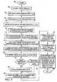
- Fig. 5depicts a flowchart describing an operational flow, in accordance with an exemplary embodiment of the invention
- Fig. 6depicts a timing diagram for a reading of high resistance in a sensed memory cell, in accordance with an exemplary embodiment of the invention
- Fig. 7depicts a timing diagram for a reading of low resistance in a sensed memory cell, in accordance with an exemplary embodiment of the invention.
- Fig. 8depicts a block diagram of a processor-based system containing a PCRAM memory, in accordance with an exemplary embodiment of the invention.
- a pair of memory arraysare coupled to a respective plurality of sense amplifiers where each memory array is made up of a plurality of programmable conductor memory cells.
- an appropriate voltage differencemust be placed across the programmable conductor memory element. The voltage difference must be sufficient to enable a read operation of the programmable conductor memory element, but insufficient to enable the element to be programmed (or written to).
- a digit (bit) line voltage valueis discharged through the memory cell and through the programmable conductor memory element.
- Fig. 1provides greater detail of an exemplary embodiment of the invention.
- Fig. 1depicts a portion of a pair of memory arrays 100, 165, each having a plurality of columns 108, 112, 106, 110 and rows 122, 126, 128, 124, 130, 132. At each intersection of columns and rows there is formed a programmable conductor random access memory (PCRAM) cell such as memory cell 120.
- PCRAMprogrammable conductor random access memory
- Sense amplifier 102receives inputs from column line 108 and column line 106.
- Sense amplifier 104receives inputs from column line 112 and column line 110.
- Each sense amplifier 102, 104is configured to compare a voltage at a digit (bit) line (e.g., 108) of a cell 120 being read with a voltage at a reference line (e.g., 106) in order to determine whether the sensed memory cell 120 is storing a value of logic HIGH or logic LOW.
- bitdigit
- reference linee.g. 106
- a voltage at digit line 108is compared with a reference voltage on complementary digit line 106 by sense amplifier 102.
- the digit line 108 or 106acts as the digit line D and the digit line 106 on the other side acts as the reference digit line D*.
- memory cell 120is the cell being sensed.
- the column line 108 associated with memory cell 120is referred to as the digit (bit) line D.
- Column line 106is referred to as the digit complement line D*, or the reference line.
- Each programmable conductor memory cell 120consists of an access transistor 114 and a programmable conductor memory element 116. One end of the programmable conductor memory element 116 is coupled to a cell plate 118. The other end of the programmable conductor memory element 116 is coupled to a source/drain terminal of access transistor 114. Another source/drain terminal of access transistor 114 is coupled to digit line 108. A gate of the access transistor 114 is coupled to a rowline 122 associated with the memory cell 120.
- the D and D* linesare coupled to a pre-charging circuit 175 for precharging the D and D* lines to a predetermined voltage value (e.g., Vdd).
- the D* lineis coupled to one terminal of p-type complementary metal oxide semiconductor (CMOS) transistor 177 and another terminal of transistor 177 is coupled to Vdd.
- the D lineis coupled to one terminal of p-type CMOS transistor 179 and another terminal of transistor 179 is coupled to Vdd.
- the gates of both transistors 177, 179are coupled together for receiving a precharge control signal. When the precharge control signal is received, both transistors 177, 179 are turned on and both the digit line D and digit-complement line D* are charged to Vdd.
- FIG. 1also shows an equilibrate circuit 176 for equalizing the voltage on the D and D* digit lines. After the D and D* are precharged to Vdd by a precharge signal, the lines are then equilibrated by an equilibrate EQ signal applied to transistor 180.
- a simplified schematic diagram of programmable conductor memory cell 120is depicted.
- digit line D 108is coupled to Vdd during precharge and also coupled to a first terminal of access transistor 114.
- Access transistor 114is depicted as n-type CMOS transistor; however, access transistor 114 may easily be replaced with a p-type CMOS transistor as long as the corresponding polarities of the other components and voltages are modified accordingly.
- a second terminal of transistor 114is coupled to a first terminal of programmable conductor memory element 116.
- programmable conductor memory element 116may be made of chalcogenide glass, or any other bistable resistive material that allows for the storage of binary values.
- the programmable conductor memory element 116is coupled to cell plate 118 which is also a common conductor for a plurality of programmable conductor memory elements.
- the cell plate 118is tied to a voltage terminal for providing a predetermined voltage level (e.g., Vdd/2) to the cell plate 118.
- a gate of access transistor 114is tied to rowline 122. When sufficient voltage is applied to rowline 122, access transistor 114 is turned on and conducting and couples the digit line D 108 to the programmable conductor memory element 116.
- the voltage value applied to rowline 122dictates what operation is being performed on the programmable conductor memory element 116. For instance, assuming the D line 108 is tied to Vdd (e.g., 2.5V) and the cell plate is tied to 1 ⁇ 2 Vdd (e.g., 1.25V), in order to activate the access transistor 114, a minimum of 2.05V must be applied to its gate. A voltage of 2.05V at the gate of access transistor 114 is sufficient to turn on transistor 114 since that creates a difference of potential of at least the threshold voltage (Vt), approximately 0.8V, between the gate and the source/drain terminal coupled to the cell plate 118.
- Vtthreshold voltage
- While 2.05V applied to the gate of access transistor 114is sufficient to turn it on, it is not sufficient for reading from or writing to the programmable conductor memory cell 120.
- approximately 0.2Vis required to be across the programmable conductor memory element 116 in order to read it.
- writee.g., re-program its value
- a minimum of 0.25Vis required to be across it and the polarity of the 0.25V depends on whether a logic HIGH or a logic LOW is being rewritten to the memory element 116.
- Fig. 2(b)the voltage levels and their polarities are discussed in greater detail.
- a voltage of approximately 2.25Vis applied to the rowline 122 coupled to the gate of access transistor 122.
- the threshold voltage, Vtis subtracted from 2.25V and point A is approximately 1.45V.
- the cell platebeing at 1.25V leaves a voltage drop of 0.2V across the programmable conductor memory element 116; a voltage sufficient for reading the contents of the element 116, but insufficient for writing to the element 116.
- Fig. 2(c)depicts exemplary voltage levels and polarities for writing a logic LOW back into the programmable conductor memory element 116.
- the D line 108is grounded by the sense amplifier 102.
- Point Ais also at approximately ground and, therefore, a voltage drop of approximately -1.25V is across the programmable contact and the logic LOW may be rewritten back into the programmable conductor memory element 116.
- Fig. 2(d)depicts exemplary voltage levels and polarities for writing a logic HIGH back into the programmable conductor memory element 116.
- the D line 108is boosted to approximately Vdd by the sense amplifier 102.
- the rowline 122is raised from approximately 2.25V (its voltage level during the read operation) to approximately Vdd, thereby placing a voltage of approximately 1.7V at point A.
- the 1.7V at point Acreates a potential difference of approximately 0.45V across the programmable conductor memory element 116 in order to rewrite the logic HIGH level.
- the sense amplifier 102includes an N-sense amplifier portion and a P-sense amplifier portion.
- Fig. 3depicts the N-sense amplifier portion 350.
- a first terminal of N-sense amplifier 350receives digit complement line D* (i.e., the column line in the memory array adjacent to the memory array that contains the memory cell of interest) and is also coupled to a gate of n-type CMOS transistor 305 and a first terminal of n-type CMOS transistor 300.
- a second terminal of N-sense amplifier 350receives digit line D (i.e., the column line in the memory array that contains the cell of interest) and is also coupled to a gate of transistor 300 and a first terminal of transistor 305.
- a second terminal of transistor 300 and a second terminal of transistor 305are coupled to a first terminal of CMOS transistor 310.
- a second terminal of transistor 310is coupled to ground and a gate of transistor 310 receives a Fire N control signal.
- the Fire N control signalis received by the N-sense amplifier 350 a predetermined time after the desired memory cell rowline is fired, as will be described below.
- Fig. 4depicts a P-sense amplifier portion 360 of a sense amplifier such as sense amplifier 102.
- a first terminal of P-sense amplifier 360receives digit complement line D* and is also coupled to a gate of p-type CMOS transistor 330 and a first terminal of p-type CMOS transistor 325.
- a second terminal of P-sense amplifier 360receives digit line D and is also coupled to a gate of transistor 325 and a first terminal of transistor 330.
- a second terminal of transistor 325 and a second terminal of transistor 330are coupled to a first terminal of transistor 320.
- a gate of transistor 320receives a Fire P control signal. The Fire P control signal is received by the P-sense amplifier 360 a predetermined time after the Fire N control signal is received by the N-sense amplifier 350.
- Fig. 5a flowchart describing an operational flow of the Figs. 1 and 2 schematic diagrams is depicted, in accordance with an exemplary embodiment of the invention.
- the following parameters of the PCRAM cellare presumed: i) that the erase voltage to grow a dendrite in programmable conductor memory element 116 switching it to a high resistance state and thus write a logic "1" is 0.25V; (ii) that the erase current is approximately 10 ⁇ A; (iii) that the program voltage (write a "1" element to logic "0") is -0.25V; (iv) that the program current is approximately 10 ⁇ A; (v) that the resistance corresponding to a logic "0" is approximately 10K ⁇ ; and (vi) that the resistance corresponding to a logic "1” is any value greater than approximately 10M ⁇ .
- alternative parameters and operating voltages and resistancesmay be selected for the PCRAM cell without departing from the scope of the invention.
- sense amplifier 102sees the two lines D and D*, where both D and D* are respective column lines 108, 106 from different memory arrays 100, 165.
- Vddis approximately 2.5V.
- the cell plate 118is tied to a predetermined voltage (e.g., Vdd/2, or approximately 1.25V) which is either a condition which is present whenever the memory is active, or one which can be switched to by memory operation.
- the Vdd/2 voltageis turned on at processing segment 506.
- a selected rowline 122is fired at segment 510 by applying a predetermined voltage from a rowline decoder to that rowline 122.
- the predetermined voltagehas been selected to be approximately 2.25V as will be described herein.
- a voltage of approximately 0.2Vmust be present across the element 116. This means that a voltage of approximately 2.25V must be applied to the rowline 122.
- a voltage of approximately 2.25V applied to rowline 122turns on transistor 114.
- the threshold voltage of transistor 114is approximately 0.8V, then a voltage of approximately 1.45V is present at point A while a voltage of approximately 1.25V is present at the cell plate 118 for a difference of approximately 0.2V, the required read voltage, as indicated at segment 512 of Fig. 5 .
- the parasitic capacitance 138may be varied as a function of the construction of the memory cell or an additional capacitance in the form of a fabricated capacitor can also be provided which is switched in circuit and connected with digit line D 108 during a read operation; therefore, in accordance with an exemplary embodiment of the invention, the amount of voltage increase when the rowline 122 is fired can be controlled by the memory architecture.
- the increase in the voltage at D 108is described at segment 514.
- a dummy row line 124could be employed in the memory array that is not of interest (e.g., 165) such that the dummy rowline 124 is always on and precharged to Vdd (approximately 2.5V). Then, when the desired rowline 122 is fired, and the desired digit line D 108 is raised to approximately 2.6V, due to the parasitic capacitance 138, the dummy rowline 124 is turned off and, as a result, the voltage at digit complement line D* 106 drops to approximately 2.4V due to the parasitic capacitance 138 between the dummy rowline 124 and column line 106. The end result is that D 108 and D* 106 differ by at least approximately 0.2V when D 108 begins to discharge as described below.
- the digit line of interest D 108begins to discharge from approximately 2.6V through the resistance of the programmable conductor memory element down to approximately 1.25V, the cell plate 118 voltage. The longer the discharge operation takes, the greater the resistance level of the programmable conductor memory element 116.
- a predetermined timee.g., 15-30ns
- the N-sense amplifier 350is enabled, via control signal Fire N, at segment 518 which compares the voltage on the D 108 and D* 106 lines.
- a determinationis made as to whether the programmable conductor element 116 has a low or high resistance level.
- the voltage values at D* 106 and D 108are respectively fed to gates of transistors 305 and 300. If at the predetermined time t 2 , the voltage at the digit line D 108 is higher than the voltage at the digit complement line D* 106, then D* 106 is grounded and D remains floating and considered as having a high resistance level (e.g., logic HIGH) at segment 524.
- rowline 122may be turned off after the access transistor 114 is turned on. Doing so, however, will present the programmable conductor memory element 116 from being re-written. This may be desired when a logic HIGH was read since a re-write may not be desired after each read operation of a logic HIGH as this is the normal state of the programmable conductor memory element 116 and repeated unnecessary re-writing may result in damage to the element 116 over time.
- segment 522if at the predetermined time t 2 , the voltage at D 108 is lower than that at D* 106, then line D 108 is grounded and D 108 is considered as having a low resistance level (e.g., logic LOW) at segment 526.
- a low resistance levele.g., logic LOW
- P-sense amplifier 360is enabled, via control signal Fire P, a predetermined time (e.g., 1-5ns) t 3 after the N-sense amplifier 350 is enabled. If a high resistance level was recognized at segment 524 (i.e., D 108 is logic HIGH), then transistor 330 is on and transistor 325 is off and the voltage at line D 108 is boosted to approximately Vdd at segment 530.
- transistor 330is off and transistor 325 is on and line D* 106 is maintained at approximately Vdd at segment 532.
- the rowline 122 voltageis raised to approximately Vdd. If the programmable conductor memory element 116 contained a low resistive state, then, as described above, raising the rowline 122 voltage to approximately Vdd is not necessary to re-write a low resistive state; however, the rowline 122 is nonetheless raised in order to facilitate re-writing a high resistance state. That is, if the programmable conductor memory element 116 contained a high resistive state, then raising the rowline 122 to approximately Vdd sets the voltage at point A to approximately 1.7V, thereby placing a voltage potential difference of approximately 0.45V across the programmable conductor memory element 116 which is sufficient for re-writing.
- Fig. 6depicts a timing diagram showing a process flow for finding a high resistance level, as described in connection with a portion of Fig. 5 .
- both D 108 and D* 106are precharged to approximately Vdd.
- rowline 122fires and turns on transistor 114.
- the voltage at D 108increases by approximately 0.1V to approximately 2.6V due to the parasitic capacitance 138 between rowline 122 and column line 108.
- line D 108is discharged from approximately 2.6V for approximately 15-30ns while line D* 106 is maintained at approximately Vdd.
- N-sense amplifier 350is enabled and compares the voltage at line D 108 with that of line D* 106.
- Fig. 7depicts a timing diagram showing a process flow for finding a low resistance level, as described in connection with a portion of Fig. 5 .
- both line D 108 and line D* 106are precharged to approximately Vdd.
- rowline 122fires and turns on transistor 114.
- the voltage at D 108increases by approximately 0.1V to approximately 2.6V due to parasitic capacitance 138.
- D 108is discharged from approximately 2.6V for approximately 15-30ns while D* 106 is maintained at approximately Vdd.
- N-sense amplifier 350is enabled and compares the voltage at line D 108 with that of line D* 106.
- Fig. 8illustrates a block diagram of a processor system 800 containing a PCRAM semiconductor memory as described in connection with Figs. 1-7 .
- the PCRAM memory arrays 100, 165 described in connection with Figs. 1-7may be part of random access memory (RAM) 808 which may be constructed as a plug-in module containing one or more memory devices having the PCRAM structure described above.
- the processor-based system 800may be a computer system or any other processor system.
- the system 800includes a central processing unit (CPU) 802, e.g., a microprocessor, that communicates with floppy disk drive 812, CD ROM drive 814, and RAM 808 over a bus 820.
- CPUcentral processing unit
- bus 820may be a series of buses and bridges commonly used in a processor-based system, but for convenience purposes only, the bus 820 has been illustrated as a single bus.
- An input/output (I/O) devicee.g., monitor 804, 806 may also be connected to the bus 820, but are not required in order to practice the invention.
- the processor-based system 800also includes a read-only memory (ROM) 800 which may also be used to store a software program.
- ROMread-only memory
- Fig. 8 block diagramdepicts only one CPU 802
- the Fig. 8 systemcould also be configured as a parallel processor machine for performing parallel processing.
- parallel processor machinescan be classified as single instruction/multiple data (SIMD), meaning all processors execute the same instructions at the same time, or multiple instruction/multiple data (MIMD), meaning each processor executes different instructions.
- SIMDsingle instruction/multiple data
- MIMDmultiple instruction/multiple data
- the present inventionprovides a PCRAM cell 120 and a method for reading the contents of the memory cell 120.
- the memory cell 120consists of a programmable conductor memory element 116 in series with a first terminal of an access transistor 114.
- the other side of the programmable conductor memory element 116is coupled to a cell plate 118 that may extend across a plurality of programmable conductor memory elements 116.
- a second terminal of the access transistor 114is coupled to a column line 108, which can be the desired digit line (D).
- the gate of the transistor 114is coupled to the rowline 122 of the memory cell 120.
- a first predetermined voltage potential(e.g., Vdd) is applied to digit line D 108 and a reference digit line D* 106 of an adjacent memory array 165.
- a second predetermined voltage potentialis applied to the cell plate 118.
- the access transistor 114is turned on and conducts and digit line D 108 discharges for a predetermined time period (e.g., 15-30ns) at which time, line D 108 and line D* 106 are compared with each other, with sense amplifier 102, in order to determine whether the programmable conductor element 116 contains a high or low resistance level.
- the memory cell 120 being readis then prepared for a next cycle by precharging both line D 108 and line D* 106, as well as the rowline 122 voltage, up to approximately Vdd so that the high resistance level may be rewritten to the memory cell 120 if the memory cell did in fact have a high resistance level. If the memory cell 120 had a low resistance level, then raising the voltage potentials of lines D 108 and D* 106 and the rowline 122 will have no effect on the resistance of the memory cell 120.
Landscapes
- Semiconductor Memories (AREA)
- Read Only Memory (AREA)
- Dram (AREA)
- Techniques For Improving Reliability Of Storages (AREA)
- Programmable Controllers (AREA)
Abstract
Description
- The present invention relates to integrated memory circuits. More specifically it relates to a method for sensing the content of a programmable conductor random access memory (PCRAM) cell.
- DRAM integrated circuit arrays have existed for more than thirty years and their dramatic increase in storage capacity has been achieved through advances in semiconductor fabrication technology and circuit design technology. The tremendous advances in these two technologies have also achieved higher and higher levels of integration that permit dramatic reductions in memory array size and cost, as well as increased process yield.
- A DRAM memory cell typically comprises, as basic components, an access transistor (switch) and a capacitor for storing a binary data bit in the form of a charge. Typically, a charge of one polarity is stored on the capacitor to represent a logic HIGH (e.g., binary "1"), and a stored charge of the opposite polarity represents a logic LOW (e.g., binary "0"). The basic drawback of a DRAM is that the charge on the capacitor eventually leaks away and therefore provisions must be made to "refresh" the capacitor charge or else the data bit stored by the memory cell is lost.
- The memory cell of a conventional SRAM, on the other hand, composes, as basic components, an access transistor or transistors and a memory element in the form of two or more integrated circuit devices interconnected to function as a bistable latch. An example of such a bistable latch is cross-coupled inverters. Bistable latches do not need to be "refreshed," as in the case of DRAM memory cells, and will reliably store a data bit indefinitely as long as they continue to receive supply voltage.
- Efforts continue to identify other forms of non-volatile or semi-volatile memory elements. Recent studies have focused on resistive materials that can be programmed to exhibit either high or low stable ohmic states. A programmable resistance element of such material could be programmed (set) to a high resistive state to store, for example, a binary "1" data bit or programmed to a low resistive state to store a binary "0" data bit. The stored data bit could then be retrieved by detecting the magnitude of a readout current switched through the resistive memory element by an access device, thus indicating the stable resistance state it had previously been programmed to.
- Recently programmable conductor memory elements have been devised. For example, chalcogenide glasses which have switchable resistive states have been investigated as data storage memory cells for use in memory devices, such as DRAM memory devices,
U.S. Patents 5,761,115 ,5,896,312 ,5,914,893 , and6,084,796 all describe this technology,
One characteristic of a programmable conductor memory element such as one formed of the chalcogenide glasses described above is that it typically includes chalcogenide glass which can be doped with metal ions and a cathode and anode spaced apart on one or more surfaces of the glass. The doped glass has a normal and stable high resistance state. Application of a voltage across the cathode and anode causes a stable low resistance path to occur in the glass. Thus, stable low and high resistance states can be used to store binary data. - A programmable conductor memory element formed of a doped chalcogenide glass material typically has a stable high resistance state which may be programmed to a low resistance state by applying a voltage across the memory element. To restore the memory cell to a high resistive state, typically one needs to program the cell with a negative, or inverse voltage which is equal to or greater that the voltage used to program the memory element to the low resistance state. One particularly promising programmable conductor chalcogenide glass has a Ge:Se glass composition and is doped with silver.
- In order to realize a functional programmable conductor memory, appropriate read circuitry is required to non-destructively sense data stored in the memory elements of the array.
US 6,314,014 discloses a system for reading the state of a programmable resistance element which (with reference to Figure 1A ofUS 6,314,014 ) compares a sense signal generated by the element with a reference voltage at a node N1, combining the output of a plurality of reference cells.US 5,883,827 discloses another system for reading from an array of programmable resistance elements.- The present invention provides a method of sensing a stored value of a variable resistance memory element, as defined in the attached
Claim 1. Optional features of the method are defined in the attached Claims 2-30. - A semiconductor memory structure is also provided, as defined in the attached Claim 31. Optional features of the structure are defined in the attached Claims 32-38.
- The foregoing and other advantages and features of the invention will become more apparent from the detailed description of preferred embodiments of the invention given below with reference to the accompanying drawings in which:
Fig. 1 depicts two memory arrays each employing a plurality of PCRAM memory cells, in accordance with an exemplary embodiment of the invention;Figs. 2(a) - 2(d) each depict a PCRAM memory cell ofFig. 1 ;Fig. 3 depicts an N-sense amplifier as used in theFig. 1 memory array;Fig. 4 depicts a P-sense amplifier as used in theFig. 1 memory array;Fig. 5 depicts a flowchart describing an operational flow, in accordance with an exemplary embodiment of the invention;Fig. 6 depicts a timing diagram for a reading of high resistance in a sensed memory cell, in accordance with an exemplary embodiment of the invention;Fig. 7 depicts a timing diagram for a reading of low resistance in a sensed memory cell, in accordance with an exemplary embodiment of the invention; andFig. 8 depicts a block diagram of a processor-based system containing a PCRAM memory, in accordance with an exemplary embodiment of the invention.- The present invention will be described as set forth in exemplary embodiments described below in connection with
Figs. 1-8 . Other embodiments may be realized and other changes may be made to the disclosed embodiments without departing from the scope of the present invention. - In accordance with an exemplary embodiment of the invention, a pair of memory arrays are coupled to a respective plurality of sense amplifiers where each memory array is made up of a plurality of programmable conductor memory cells. In order to read a logical state of a given memory cell, an appropriate voltage difference must be placed across the programmable conductor memory element. The voltage difference must be sufficient to enable a read operation of the programmable conductor memory element, but insufficient to enable the element to be programmed (or written to). Once the appropriate voltage difference exists across the memory element, a digit (bit) line voltage value is discharged through the memory cell and through the programmable conductor memory element. A predetermined period of time after the discharging begins, a comparison is made, via a sense amplifier associated with the given memory cell, between the digit line voltage and a digit complement reference voltage at a reference bit line.
- If after the predetermined time, the digit line voltage is higher than the voltage at the reference line, then a high resistive state is detected and the reference line is grounded. If, however, the digit line voltage is lower than the voltage at the
reference line 106, then a low resistive state is detected and the digit line is grounded. The reference voltage is supplied by a digit complement line associated with an adjacent memory array. The two adjacent memory arrays respectively serve as sources for the a reference voltage when the other of the two memory arrays contains a selected memory cell.Fig. 1 provides greater detail of an exemplary embodiment of the invention. Fig. 1 depicts a portion of a pair ofmemory arrays columns rows memory cell 120.Sense amplifier 102 receives inputs fromcolumn line 108 andcolumn line 106.Sense amplifier 104 receives inputs fromcolumn line 112 andcolumn line 110. Eachsense amplifier cell 120 being read with a voltage at a reference line (e.g., 106) in order to determine whether thesensed memory cell 120 is storing a value of logic HIGH or logic LOW. In theFig. 1 arrangement, ifcell 120 is being read, a voltage atdigit line 108 is compared with a reference voltage oncomplementary digit line 106 bysense amplifier 102.- Depending upon which side of the
sense amplifier 102 contains thememory cell 120 of interest, thedigit line digit line 106 on the other side acts as the reference digit line D*. In this example, it is assumed thatmemory cell 120 is the cell being sensed. Thecolumn line 108 associated withmemory cell 120 is referred to as the digit (bit) line D. Columnline 106 is referred to as the digit complement line D*, or the reference line. - Each programmable
conductor memory cell 120 consists of anaccess transistor 114 and a programmableconductor memory element 116. One end of the programmableconductor memory element 116 is coupled to acell plate 118. The other end of the programmableconductor memory element 116 is coupled to a source/drain terminal ofaccess transistor 114. Another source/drain terminal ofaccess transistor 114 is coupled todigit line 108. A gate of theaccess transistor 114 is coupled to arowline 122 associated with thememory cell 120. - Further, the D and D* lines are coupled to a
pre-charging circuit 175 for precharging the D and D* lines to a predetermined voltage value (e.g., Vdd). The D* line is coupled to one terminal of p-type complementary metal oxide semiconductor (CMOS)transistor 177 and another terminal oftransistor 177 is coupled to Vdd. The D line is coupled to one terminal of p-type CMOS transistor 179 and another terminal oftransistor 179 is coupled to Vdd. The gates of bothtransistors transistors Fig. 1 also shows anequilibrate circuit 176 for equalizing the voltage on the D and D* digit lines. After the D and D* are precharged to Vdd by a precharge signal, the lines are then equilibrated by an equilibrate EQ signal applied totransistor 180. - Turning to
Fig. 2(a) , a simplified schematic diagram of programmableconductor memory cell 120 is depicted. Using therepresentative cell 120 to describe the invention,digit line D 108 is coupled to Vdd during precharge and also coupled to a first terminal ofaccess transistor 114.Access transistor 114 is depicted as n-type CMOS transistor; however,access transistor 114 may easily be replaced with a p-type CMOS transistor as long as the corresponding polarities of the other components and voltages are modified accordingly. A second terminal oftransistor 114 is coupled to a first terminal of programmableconductor memory element 116. As mentioned above, programmableconductor memory element 116 may be made of chalcogenide glass, or any other bistable resistive material that allows for the storage of binary values. The programmableconductor memory element 116 is coupled tocell plate 118 which is also a common conductor for a plurality of programmable conductor memory elements. Thecell plate 118 is tied to a voltage terminal for providing a predetermined voltage level (e.g., Vdd/2) to thecell plate 118. A gate ofaccess transistor 114 is tied torowline 122. When sufficient voltage is applied torowline 122,access transistor 114 is turned on and conducting and couples thedigit line D 108 to the programmableconductor memory element 116. - The voltage value applied to rowline 122 dictates what operation is being performed on the programmable
conductor memory element 116. For instance, assuming theD line 108 is tied to Vdd (e.g., 2.5V) and the cell plate is tied to ½ Vdd (e.g., 1.25V), in order to activate theaccess transistor 114, a minimum of 2.05V must be applied to its gate. A voltage of 2.05V at the gate ofaccess transistor 114 is sufficient to turn ontransistor 114 since that creates a difference of potential of at least the threshold voltage (Vt), approximately 0.8V, between the gate and the source/drain terminal coupled to thecell plate 118. - While 2.05V applied to the gate of
access transistor 114 is sufficient to turn it on, it is not sufficient for reading from or writing to the programmableconductor memory cell 120. In accordance with an exemplary embodiment of the invention, approximately 0.2V is required to be across the programmableconductor memory element 116 in order to read it. Further, in order to write (e.g., re-program its value) to the programmableconductor memory element 116, a minimum of 0.25V is required to be across it and the polarity of the 0.25V depends on whether a logic HIGH or a logic LOW is being rewritten to thememory element 116. - Turning to
Fig. 2(b) , the voltage levels and their polarities are discussed in greater detail. For a read operation, since approximately 0.2V is required across the programmableconductor memory element 116, a voltage of approximately 2.25V is applied to therowline 122 coupled to the gate ofaccess transistor 122. The threshold voltage, Vt, is subtracted from 2.25V and point A is approximately 1.45V. The cell plate being at 1.25V leaves a voltage drop of 0.2V across the programmableconductor memory element 116; a voltage sufficient for reading the contents of theelement 116, but insufficient for writing to theelement 116. Fig. 2(c) depicts exemplary voltage levels and polarities for writing a logic LOW back into the programmableconductor memory element 116. As will be described in greater detail below, when a logic LOW level has been read as being stored by the programmableconductor memory cell 120, theD line 108 is grounded by thesense amplifier 102. Point A is also at approximately ground and, therefore, a voltage drop of approximately -1.25V is across the programmable contact and the logic LOW may be rewritten back into the programmableconductor memory element 116.Fig. 2(d) depicts exemplary voltage levels and polarities for writing a logic HIGH back into the programmableconductor memory element 116. As will be described in greater detail below, when a logic HIGH level has been read as being stored by the programmableconductor memory cell 120, theD line 108 is boosted to approximately Vdd by thesense amplifier 102. Then, therowline 122 is raised from approximately 2.25V (its voltage level during the read operation) to approximately Vdd, thereby placing a voltage of approximately 1.7V at point A. The 1.7V at point A creates a potential difference of approximately 0.45V across the programmableconductor memory element 116 in order to rewrite the logic HIGH level.- Referring back to
Fig. 1 , thesense amplifier 102 includes an N-sense amplifier portion and a P-sense amplifier portion.Fig. 3 depicts the N-sense amplifier portion 350. A first terminal of N-sense amplifier 350 receives digit complement line D* (i.e., the column line in the memory array adjacent to the memory array that contains the memory cell of interest) and is also coupled to a gate of n-type CMOS transistor 305 and a first terminal of n-type CMOS transistor 300. A second terminal of N-sense amplifier 350 receives digit line D (i.e., the column line in the memory array that contains the cell of interest) and is also coupled to a gate oftransistor 300 and a first terminal oftransistor 305. A second terminal oftransistor 300 and a second terminal oftransistor 305 are coupled to a first terminal ofCMOS transistor 310. A second terminal oftransistor 310 is coupled to ground and a gate oftransistor 310 receives a Fire N control signal. The Fire N control signal is received by the N-sense amplifier 350 a predetermined time after the desired memory cell rowline is fired, as will be described below. Fig. 4 depicts a P-sense amplifier portion 360 of a sense amplifier such assense amplifier 102. A first terminal of P-sense amplifier 360 receives digit complement line D* and is also coupled to a gate of p-type CMOS transistor 330 and a first terminal of p-type CMOS transistor 325. A second terminal of P-sense amplifier 360 receives digit line D and is also coupled to a gate oftransistor 325 and a first terminal oftransistor 330. A second terminal oftransistor 325 and a second terminal oftransistor 330 are coupled to a first terminal oftransistor 320. A gate oftransistor 320 receives a Fire P control signal. The Fire P control signal is received by the P-sense amplifier 360 a predetermined time after the Fire N control signal is received by the N-sense amplifier 350.- Turning to
Fig. 5 , a flowchart describing an operational flow of theFigs. 1 and2 schematic diagrams is depicted, in accordance with an exemplary embodiment of the invention. In this exemplary process flow, the following parameters of the PCRAM cell are presumed: i) that the erase voltage to grow a dendrite in programmableconductor memory element 116 switching it to a high resistance state and thus write a logic "1" is 0.25V; (ii) that the erase current is approximately 10µA; (iii) that the program voltage (write a "1" element to logic "0") is -0.25V; (iv) that the program current is approximately 10µA; (v) that the resistance corresponding to a logic "0" is approximately 10KΩ; and (vi) that the resistance corresponding to a logic "1" is any value greater than approximately 10MΩ. It should be readily apparent that alternative parameters and operating voltages and resistances may be selected for the PCRAM cell without departing from the scope of the invention. - The process begins at
process segment 500. Atsegment 502,sense amplifier 102 sees the two lines D and D*, where both D and D* arerespective column lines different memory arrays cell plate 118 is tied to a predetermined voltage (e.g., Vdd/2, or approximately 1.25V) which is either a condition which is present whenever the memory is active, or one which can be switched to by memory operation. In this illustrated embodiment, the Vdd/2 voltage is turned on atprocessing segment 506. Atsegment 508, both lines D, D* 108, 106 are precharged to a predetermined voltage (e.g., Vdd = approximately 2.5 V) viaprecharge circuit 175 and then equilibrated byequilibrate circuit 176. - A selected
rowline 122 is fired atsegment 510 by applying a predetermined voltage from a rowline decoder to thatrowline 122. In this example, the predetermined voltage has been selected to be approximately 2.25V as will be described herein. In order to read the contents of thememory cell 120, or more specifically, in order to read the resistance of the programmableconductor memory element 116 of thememory cell 120, a voltage of approximately 0.2V must be present across theelement 116. This means that a voltage of approximately 2.25V must be applied to therowline 122. A voltage of approximately 2.25V applied torowline 122 turns ontransistor 114. Since the threshold voltage oftransistor 114 is approximately 0.8V, then a voltage of approximately 1.45V is present at point A while a voltage of approximately 1.25V is present at thecell plate 118 for a difference of approximately 0.2V, the required read voltage, as indicated atsegment 512 ofFig. 5 . - It should be mentioned that when
access transistor 114 is conducting, the voltage of thedigit line D 108 is actually increased by approximately 0.1V (up to approximately 2.6V) due to a parasitic capacitance (e.g., 138 ofFig. 1 ) inherent between thecolumn line 108 and therowline 122 of the memory cell. This results in approximately a 0.1V difference between digit line D, thecolumn line 108 associated with the cell being read 120, and D* 106, the reference digit line. Theparasitic capacitance 138 may be varied as a function of the construction of the memory cell or an additional capacitance in the form of a fabricated capacitor can also be provided which is switched in circuit and connected withdigit line D 108 during a read operation; therefore, in accordance with an exemplary embodiment of the invention, the amount of voltage increase when therowline 122 is fired can be controlled by the memory architecture. The increase in the voltage atD 108 is described atsegment 514. - There are other ways to increase the voltage difference between D and D*, as seen by the
sense amplifier 102. For instance, adummy row line 124 could be employed in the memory array that is not of interest (e.g., 165) such that thedummy rowline 124 is always on and precharged to Vdd (approximately 2.5V). Then, when the desiredrowline 122 is fired, and the desireddigit line D 108 is raised to approximately 2.6V, due to theparasitic capacitance 138, thedummy rowline 124 is turned off and, as a result, the voltage at digit complement line D* 106 drops to approximately 2.4V due to theparasitic capacitance 138 between the dummy rowline 124 andcolumn line 106. The end result is thatD 108 and D* 106 differ by at least approximately 0.2V whenD 108 begins to discharge as described below. - Still referring to
Fig. 5 , atsegment 516, the digit line ofinterest D 108 begins to discharge from approximately 2.6V through the resistance of the programmable conductor memory element down to approximately 1.25V, thecell plate 118 voltage. The longer the discharge operation takes, the greater the resistance level of the programmableconductor memory element 116. A predetermined time (e.g., 15-30ns) after the selectedrowline 122 is fired, atsegment 510, the N-sense amplifier 350 is enabled, via control signal Fire N, atsegment 518 which compares the voltage on theD 108 and D* 106 lines. Atsegment 520, a determination is made as to whether theprogrammable conductor element 116 has a low or high resistance level. - For example, at
segment 522, a determination is made as to whether the initial voltage onD 108 has discharged below the voltage on D* 106 in the predetermined timeframe (e.g., 15-30ns). Referring back toFig. 3 , the voltage values at D* 106 andD 108 are respectively fed to gates oftransistors digit line D 108 is higher than the voltage at the digit complement line D* 106, then D* 106 is grounded and D remains floating and considered as having a high resistance level (e.g., logic HIGH) atsegment 524. - It should be noted that
rowline 122 may be turned off after theaccess transistor 114 is turned on. Doing so, however, will present the programmableconductor memory element 116 from being re-written. This may be desired when a logic HIGH was read since a re-write may not be desired after each read operation of a logic HIGH as this is the normal state of the programmableconductor memory element 116 and repeated unnecessary re-writing may result in damage to theelement 116 over time. - Still referring to
segment 522, if at the predetermined time t2, the voltage atD 108 is lower than that at D* 106, thenline D 108 is grounded andD 108 is considered as having a low resistance level (e.g., logic LOW) atsegment 526. - At
segment 528, P-sense amplifier 360 is enabled, via control signal Fire P, a predetermined time (e.g., 1-5ns) t3 after the N-sense amplifier 350 is enabled. If a high resistance level was recognized at segment 524 (i.e.,D 108 is logic HIGH), thentransistor 330 is on andtransistor 325 is off and the voltage atline D 108 is boosted to approximately Vdd atsegment 530. - If a low resistance level was recognized at segment 524 (i.e.,
D 108 is logic LOW), thentransistor 330 is off andtransistor 325 is on and line D* 106 is maintained at approximately Vdd atsegment 532. - At
segment 534, therowline 122 voltage is raised to approximately Vdd. If the programmableconductor memory element 116 contained a low resistive state, then, as described above, raising therowline 122 voltage to approximately Vdd is not necessary to re-write a low resistive state; however, therowline 122 is nonetheless raised in order to facilitate re-writing a high resistance state. That is, if the programmableconductor memory element 116 contained a high resistive state, then raising therowline 122 to approximately Vdd sets the voltage at point A to approximately 1.7V, thereby placing a voltage potential difference of approximately 0.45V across the programmableconductor memory element 116 which is sufficient for re-writing. Fig. 6 depicts a timing diagram showing a process flow for finding a high resistance level, as described in connection with a portion ofFig. 5 . For example, initially, bothD 108 and D* 106 are precharged to approximately Vdd. At time t1, rowline 122 fires and turns ontransistor 114. The voltage atD 108 increases by approximately 0.1V to approximately 2.6V due to theparasitic capacitance 138 betweenrowline 122 andcolumn line 108. Then,line D 108 is discharged from approximately 2.6V for approximately 15-30ns while line D* 106 is maintained at approximately Vdd. At time t2, N-sense amplifier 350 is enabled and compares the voltage atline D 108 with that of line D* 106. If the voltage measured atD 108 is greater than that of D* 106, then a high resistance level is recognized, as described in connection withFig. 5 . In addition, line D* 106 is forced to ground (0V) at time t2. At time t3, P-sense amplifier 360 is enabled and line D is boosted to Vdd and read as logic HIGH. At time t4, therowline 122 voltage is increased from approximately 2.25 to approximately Vdd, thereby enabling the contents of theprogrammable conductor element 116 to be rewritten.Fig. 7 depicts a timing diagram showing a process flow for finding a low resistance level, as described in connection with a portion ofFig. 5 . For example, initially, bothline D 108 and line D* 106 are precharged to approximately Vdd. At time t1, rowline 122 fires and turns ontransistor 114. The voltage atD 108 increases by approximately 0.1V to approximately 2.6V due toparasitic capacitance 138. Then,D 108 is discharged from approximately 2.6V for approximately 15-30ns while D* 106 is maintained at approximately Vdd. At time t2, N-sense amplifier 350 is enabled and compares the voltage atline D 108 with that of line D* 106. If the voltage measured atD 108 is less than that of D* 106, then a low resistance level is recognized, as described in connection withFig. 5 . In addition,line D 108 is forced to ground (0V) at time t2. At time t3, P-sense amplifier 360 is enabled and line D remains at 0V and is read as logic LOW and line D* is maintained at approximately Vdd. At time t4,rowline 122 voltage is increased from approximately 2.25 to approximately Vdd. As described above, although this is not necessary to re-write a low resistance level in the programmableconductor memory element 116, it is done so that other memory cells storing a high resistance level may be rewritten.Fig. 8 illustrates a block diagram of aprocessor system 800 containing a PCRAM semiconductor memory as described in connection withFigs. 1-7 . For example, thePCRAM memory arrays Figs. 1-7 may be part of random access memory (RAM) 808 which may be constructed as a plug-in module containing one or more memory devices having the PCRAM structure described above. The processor-basedsystem 800 may be a computer system or any other processor system. Thesystem 800 includes a central processing unit (CPU) 802, e.g., a microprocessor, that communicates withfloppy disk drive 812, CD ROM drive 814, andRAM 808 over abus 820. It must be noted that thebus 820 may be a series of buses and bridges commonly used in a processor-based system, but for convenience purposes only, thebus 820 has been illustrated as a single bus. An input/output (I/O) device (e.g., monitor) 804, 806 may also be connected to thebus 820, but are not required in order to practice the invention. The processor-basedsystem 800 also includes a read-only memory (ROM) 800 which may also be used to store a software program.- Although the
Fig. 8 block diagram depicts only oneCPU 802, theFig. 8 system could also be configured as a parallel processor machine for performing parallel processing. As known in the art, parallel processor machines can be classified as single instruction/multiple data (SIMD), meaning all processors execute the same instructions at the same time, or multiple instruction/multiple data (MIMD), meaning each processor executes different instructions. - The present invention provides a
PCRAM cell 120 and a method for reading the contents of thememory cell 120. Thememory cell 120 consists of a programmableconductor memory element 116 in series with a first terminal of anaccess transistor 114. The other side of the programmableconductor memory element 116 is coupled to acell plate 118 that may extend across a plurality of programmableconductor memory elements 116. A second terminal of theaccess transistor 114 is coupled to acolumn line 108, which can be the desired digit line (D). The gate of thetransistor 114 is coupled to therowline 122 of thememory cell 120. A first predetermined voltage potential (e.g., Vdd) is applied todigit line D 108 and a reference digit line D* 106 of anadjacent memory array 165. A second predetermined voltage potential is applied to thecell plate 118. When therowline 122 for a desiredmemory cell 120 is fired with a third predetermined voltage potential (e.g., approximately 2.25V), theaccess transistor 114 is turned on and conducts anddigit line D 108 discharges for a predetermined time period (e.g., 15-30ns) at which time,line D 108 and line D* 106 are compared with each other, withsense amplifier 102, in order to determine whether theprogrammable conductor element 116 contains a high or low resistance level. Thememory cell 120 being read is then prepared for a next cycle by precharging bothline D 108 and line D* 106, as well as therowline 122 voltage, up to approximately Vdd so that the high resistance level may be rewritten to thememory cell 120 if the memory cell did in fact have a high resistance level. If thememory cell 120 had a low resistance level, then raising the voltage potentials oflines D 108 and D* 106 and therowline 122 will have no effect on the resistance of thememory cell 120. - While the invention has been described in detail in connection with preferred embodiments known at the time, it should be readily understood that the invention is not limited to the disclosed embodiments. Rather, the invention can be modified to incorporate any number of variations, alterations, substitutions or equivalent arrangements not heretofore described, but which are commensurate with the scope of the invention. For example, although the invention has been described in connection with specific voltage levels, it should be readily apparent that voltage levels very different than those described herein can be used to achieve the same results. In addition, although the invention has been described in connection with n-type and p-type CMOS transistors, it should be readily apparent that complementary CMOS transistors can be used instead. Furthermore, although the invention has been described in connection with a specific polarity for the
memory cell 120, that polarity may be reversed resulting in different voltage levels being applied to thetransistor 114,cell plate 118,digit line D 108 and digit complement line D* 106. Accordingly, the invention is not limited by the foregoing description or drawings, but is only limited by the scope of the appended claims.
Claims (38)
- A method of sending a stored value of a variable resistance memory element (116), the method comprising:precharging a digit line (D) and a digit complement line (D*) to a predetermined voltage value;activating an access transistor (114) coupled between said element (116) and said digit line (D) to apply a read voltage to said element; andcomparing the voltage on said digit line (D) with a voltage on said digit complement line (D*) to determine a resistance level, and thereby, a logical state of said element (116).
- The method of claim 1, wherein said act of precharging comprises precharging said digit line (D) and said digit complement line (D*) to approximately Vdd.
- The method of claim 1 or 2, wherein said act of precharging comprises receiving a precharge control signal at a precharge circuit and coupling said digit line and said digit complement line to approximately Vdd.
- The method of any preceding claim, wherein said act of precharging further comprises equilibrating said voltage on said digit line and said voltage on said digit complement line.
- The method of any preceding claim, wherein said act of activating comprises firing a rowline (122) coupled to a gate of said access transistor (114).
- The method of any preceding claim, further comprising discharging said voltage on said digit line (D) for a predetermined period of time before said act of comparing.
- The method of claim 6, wherein said act of discharging further comprises discharging said voltage on said digit line (D) from a voltage value approximately equal to said predetermined voltage plus an additional voltage.
- The method of claim 7, wherein said additional voltage is due to parasitic capacitance between said digit line and a rowline (122) coupled to said access transistor (114).
- The method of any preceding claim, further comprising reading a low resistance level at said element (116).
- The method of claim 9, further comprising rewriting said low resistance level into said element (116).
- The method of claim 1, further comprising reading a high resistance level at said element (116).
- The method of any preceding claim, further comprising applying a voltage to a second terminal of said memory element (116), said voltage being between 0v and said predetermined voltage.
- The method of claim 12, wherein said act of applying said voltage to a cell plate (118) tied to said second terminal of said memory element (116).
- The method of any preceding claim, further comprising:setting a voltage of a cell plate (118) of a variable resistance memory cell (120), to which a first portion of a resistive element (116) of said cell is coupled, to a first predetermined voltage;charging a first terminal of said access transistor (114) of said cell (120) and a reference conductor to a second predetermined voltage, wherein said first terminal is coupled to a column line of said cell, wherein a second terminal of said transistor (114) is coupled to a second portion of said resistive element (116), and wherein said first terminal and said reference conductor are coupled to respective inputs of a comparator (102);charging a gate of said access transistor (114) to a third predetermined voltage in order to read said cell (120), wherein said gate is coupled to a rowline of said cell;discharging said first terminal from said second predetermined voltage through the resistive element (116);comparing a voltage at said first terminal with said second predetermined voltage a predetermined period of time after said act of discharging begins in order to determine a logical state of said cell (120).
- The method of claim 14, wherein said second predetermined voltage is greater than said first predetermined voltage.
- The method of claim 14 or 15, wherein said act of discharging comprises discharging said first terminal from a fourth predetermined voltage that is slightly different from said second predetermined voltage, said fourth predetermined voltage resulting from a parasitic capacitance (138) associated with said column line (D).
- The method of any one of claims 14 to 16, further comprising changing said third predetermined voltage to a level sufficient to rewrite said resistance level to said memory cell (120) after said memory cell has been read.
- The method of claim 17, wherein said act of changing comprises increasing said third predetermined voltage to said second predetermined voltage.
- The method of claim 18, wherein said act of increasing comprises increasing said third predetermined voltage level to approximately Vdd.
- The method of claim 17, further comprising rewriting said high resistance level to said memory cell (120).
- The method of claim 14, wherein said act of setting comprises setting said voltage of said cell plate (118) to approximately Vdd.
- The method of claim 21, wherein said act of setting comprises setting said voltage of said cell plate (118) to approximately Vdd/2.
- The method of any one of claims 14 to 22, wherein said act of charging a first terminal of a transistor (114) comprises charging said first terminal and said reference conductor to approximately Vdd.
- The method of any one of claims 14 to 23, wherein said act of charging a gate comprises charging said gate to a value sufficient for reading said resistive element (116), but less than a value that would enable said cell (120) to be programmed.
- The method of claim 24, wherein said act of charging said gate comprises charging said gate to a voltage level between said first and second predetermined voltages.
- The method of claim 16, wherein said act of discharging said first terminal comprises discharging said first terminal from approximately Vdd plus an additional voltage.
- The method of claim 26, wherein said act of discharging said first terminal comprises discharging said first terminal from approximately Vdd plus approximately 0.1V.
- The method of any one of claims 14 to 27, wherein said act of comparing comprises comparing said voltage at said first terminal with said second predetermined voltage approximately 15-30ns after said act of discharging has begun.
- The method of any one of claims 14 to 28, further comprising determining said memory cell (120) has a logic HIGH state.
- The method of any one of claims 14 to 28, further comprising determining said memory cell (120) has a logic LOW state.
- A variable resistance memory structure comprising:a digit line (D) and a digit complement line (D*);a circuit for precharging said digit line (D) and said digit complement line (D*) to a predetermined voltage value prior to a read operation;an access transistor (114) for coupling a variable resistance memory element (116) to said digit line (D) during a read operation; anda sense amplifier (102) for comparing voltages on said digit line (D) and said digit complement line (D*) during said read operation to determine a resistance level, and thereby, a logical state of said memory element (116).
- The structure of claim 31, wherein said predetermined voltage is approximately Vdd.
- The structure of claim 31 or 32, wherein said variable resistance memory element comprises a chalcogenide glass having first and second electrodes.
- The structure of claim 33, wherein said chalcogenide glass has a Ge, Se and a metal ion composition.
- The structure of claim 33 or 34, wherein said chalcogenide glass has a Ge, Se and Ag composition.
- The structure of any one of claims 31 to 35, further comprising a variable parasitic capacitance (138) between said digit line (D) and a rowline (122) of said memory structure, said variable parasitic capacitance (138) causing said digit line to be charged to a voltage level higher than said predetermined voltage during said read operation.
- The structure of any one of claims 31 to 36, wherein said digit complement line (D*) is associated with a memory array different from a memory array with which said memory cell is associated.
- The structure of any one of claims 31 to 37, further comprising an equilibrate circuit for equilibrating said digit line (D) and said digit complement line (D*) to said predetermined voltage.
Applications Claiming Priority (3)
| Application Number | Priority Date | Filing Date | Title |
|---|---|---|---|
| US10/076,486US6791885B2 (en) | 2002-02-19 | 2002-02-19 | Programmable conductor random access memory and method for sensing same |
| US76486 | 2002-02-19 | ||
| PCT/US2003/003674WO2003071549A1 (en) | 2002-02-19 | 2003-02-10 | Programmable conductor random access memory and method for sensing same |
Publications (2)
| Publication Number | Publication Date |
|---|---|
| EP1476877A1 EP1476877A1 (en) | 2004-11-17 |
| EP1476877B1true EP1476877B1 (en) | 2008-05-21 |
Family
ID=27732505
Family Applications (1)
| Application Number | Title | Priority Date | Filing Date |
|---|---|---|---|
| EP03742713AExpired - LifetimeEP1476877B1 (en) | 2002-02-19 | 2003-02-10 | Programmable conductor random access memory and method for sensing same |
Country Status (10)
| Country | Link |
|---|---|
| US (2) | US6791885B2 (en) |
| EP (1) | EP1476877B1 (en) |
| JP (1) | JP4619004B2 (en) |
| KR (1) | KR100626508B1 (en) |
| CN (2) | CN101261880B (en) |
| AT (1) | ATE396482T1 (en) |
| AU (1) | AU2003210901A1 (en) |
| DE (1) | DE60321138D1 (en) |
| TW (1) | TW587250B (en) |
| WO (1) | WO2003071549A1 (en) |
Families Citing this family (122)
| Publication number | Priority date | Publication date | Assignee | Title |
|---|---|---|---|---|
| US6734455B2 (en) | 2001-03-15 | 2004-05-11 | Micron Technology, Inc. | Agglomeration elimination for metal sputter deposition of chalcogenides |
| US7102150B2 (en) | 2001-05-11 | 2006-09-05 | Harshfield Steven T | PCRAM memory cell and method of making same |
| US6951805B2 (en)* | 2001-08-01 | 2005-10-04 | Micron Technology, Inc. | Method of forming integrated circuitry, method of forming memory circuitry, and method of forming random access memory circuitry |
| US6881623B2 (en) | 2001-08-29 | 2005-04-19 | Micron Technology, Inc. | Method of forming chalcogenide comprising devices, method of forming a programmable memory cell of memory circuitry, and a chalcogenide comprising device |
| US6784018B2 (en) | 2001-08-29 | 2004-08-31 | Micron Technology, Inc. | Method of forming chalcogenide comprising devices and method of forming a programmable memory cell of memory circuitry |
| US6955940B2 (en) | 2001-08-29 | 2005-10-18 | Micron Technology, Inc. | Method of forming chalcogenide comprising devices |
| US6646902B2 (en) | 2001-08-30 | 2003-11-11 | Micron Technology, Inc. | Method of retaining memory state in a programmable conductor RAM |
| US6998696B2 (en)* | 2001-09-21 | 2006-02-14 | Casper Michael D | Integrated thin film capacitor/inductor/interconnect system and method |
| US6560155B1 (en)* | 2001-10-24 | 2003-05-06 | Micron Technology, Inc. | System and method for power saving memory refresh for dynamic random access memory devices after an extended interval |
| US6815818B2 (en) | 2001-11-19 | 2004-11-09 | Micron Technology, Inc. | Electrode structure for use in an integrated circuit |
| US6791859B2 (en) | 2001-11-20 | 2004-09-14 | Micron Technology, Inc. | Complementary bit PCRAM sense amplifier and method of operation |
| US6909656B2 (en)* | 2002-01-04 | 2005-06-21 | Micron Technology, Inc. | PCRAM rewrite prevention |
| US6867064B2 (en)* | 2002-02-15 | 2005-03-15 | Micron Technology, Inc. | Method to alter chalcogenide glass for improved switching characteristics |
| US6791885B2 (en) | 2002-02-19 | 2004-09-14 | Micron Technology, Inc. | Programmable conductor random access memory and method for sensing same |
| US6847535B2 (en) | 2002-02-20 | 2005-01-25 | Micron Technology, Inc. | Removable programmable conductor memory card and associated read/write device and method of operation |
| US6809362B2 (en) | 2002-02-20 | 2004-10-26 | Micron Technology, Inc. | Multiple data state memory cell |
| US7151273B2 (en) | 2002-02-20 | 2006-12-19 | Micron Technology, Inc. | Silver-selenide/chalcogenide glass stack for resistance variable memory |
| US7087919B2 (en) | 2002-02-20 | 2006-08-08 | Micron Technology, Inc. | Layered resistance variable memory device and method of fabrication |
| US6937528B2 (en) | 2002-03-05 | 2005-08-30 | Micron Technology, Inc. | Variable resistance memory and method for sensing same |
| US6849868B2 (en) | 2002-03-14 | 2005-02-01 | Micron Technology, Inc. | Methods and apparatus for resistance variable material cells |
| US6864500B2 (en)* | 2002-04-10 | 2005-03-08 | Micron Technology, Inc. | Programmable conductor memory cell structure |
| US6855975B2 (en) | 2002-04-10 | 2005-02-15 | Micron Technology, Inc. | Thin film diode integrated with chalcogenide memory cell |
| US6858482B2 (en) | 2002-04-10 | 2005-02-22 | Micron Technology, Inc. | Method of manufacture of programmable switching circuits and memory cells employing a glass layer |
| US6731528B2 (en)* | 2002-05-03 | 2004-05-04 | Micron Technology, Inc. | Dual write cycle programmable conductor memory system and method of operation |
| US6890790B2 (en)* | 2002-06-06 | 2005-05-10 | Micron Technology, Inc. | Co-sputter deposition of metal-doped chalcogenides |
| US6825135B2 (en) | 2002-06-06 | 2004-11-30 | Micron Technology, Inc. | Elimination of dendrite formation during metal/chalcogenide glass deposition |
| US7209378B2 (en) | 2002-08-08 | 2007-04-24 | Micron Technology, Inc. | Columnar 1T-N memory cell structure |
| US7018863B2 (en) | 2002-08-22 | 2006-03-28 | Micron Technology, Inc. | Method of manufacture of a resistance variable memory cell |
| US7294527B2 (en) | 2002-08-29 | 2007-11-13 | Micron Technology Inc. | Method of forming a memory cell |
| US6831019B1 (en) | 2002-08-29 | 2004-12-14 | Micron Technology, Inc. | Plasma etching methods and methods of forming memory devices comprising a chalcogenide comprising layer received operably proximate conductive electrodes |
| US7364644B2 (en) | 2002-08-29 | 2008-04-29 | Micron Technology, Inc. | Silver selenide film stoichiometry and morphology control in sputter deposition |
| US7163837B2 (en) | 2002-08-29 | 2007-01-16 | Micron Technology, Inc. | Method of forming a resistance variable memory element |
| US6864521B2 (en) | 2002-08-29 | 2005-03-08 | Micron Technology, Inc. | Method to control silver concentration in a resistance variable memory element |
| US7010644B2 (en) | 2002-08-29 | 2006-03-07 | Micron Technology, Inc. | Software refreshed memory device and method |
| US6867114B2 (en) | 2002-08-29 | 2005-03-15 | Micron Technology Inc. | Methods to form a memory cell with metal-rich metal chalcogenide |
| US7800932B2 (en)* | 2005-09-28 | 2010-09-21 | Sandisk 3D Llc | Memory cell comprising switchable semiconductor memory element with trimmable resistance |
| US7022579B2 (en) | 2003-03-14 | 2006-04-04 | Micron Technology, Inc. | Method for filling via with metal |
| US7050327B2 (en)* | 2003-04-10 | 2006-05-23 | Micron Technology, Inc. | Differential negative resistance memory |
| US6870784B2 (en)* | 2003-05-28 | 2005-03-22 | Micron Technology, Inc. | Integrated charge sensing scheme for resistive memories |
| US6930909B2 (en) | 2003-06-25 | 2005-08-16 | Micron Technology, Inc. | Memory device and methods of controlling resistance variation and resistance profile drift |
| US6961277B2 (en) | 2003-07-08 | 2005-11-01 | Micron Technology, Inc. | Method of refreshing a PCRAM memory device |
| US7061004B2 (en) | 2003-07-21 | 2006-06-13 | Micron Technology, Inc. | Resistance variable memory elements and methods of formation |
| US6903361B2 (en) | 2003-09-17 | 2005-06-07 | Micron Technology, Inc. | Non-volatile memory structure |
| US7050319B2 (en)* | 2003-12-03 | 2006-05-23 | Micron Technology, Inc. | Memory architecture and method of manufacture and operation thereof |
| JP4385778B2 (en)* | 2004-01-29 | 2009-12-16 | ソニー株式会社 | Storage device |
| US7583551B2 (en) | 2004-03-10 | 2009-09-01 | Micron Technology, Inc. | Power management control and controlling memory refresh operations |
| US7098068B2 (en) | 2004-03-10 | 2006-08-29 | Micron Technology, Inc. | Method of forming a chalcogenide material containing device |
| DE102004018859B3 (en)* | 2004-04-19 | 2005-09-15 | Infineon Technologies Ag | Memory storage circuit e.g. for flip flop circuit for making available video or audio data for given length of time in terminal, has memory cell with PMC resistor having solid electrolyte material with write circuit |
| KR100610008B1 (en)* | 2004-07-19 | 2006-08-08 | 삼성전자주식회사 | Phase change memory device suitable for burst read operation and data reading method accordingly |
| US7354793B2 (en) | 2004-08-12 | 2008-04-08 | Micron Technology, Inc. | Method of forming a PCRAM device incorporating a resistance-variable chalocogenide element |
| US7190048B2 (en) | 2004-07-19 | 2007-03-13 | Micron Technology, Inc. | Resistance variable memory device and method of fabrication |
| US7326950B2 (en) | 2004-07-19 | 2008-02-05 | Micron Technology, Inc. | Memory device with switching glass layer |
| US7365411B2 (en) | 2004-08-12 | 2008-04-29 | Micron Technology, Inc. | Resistance variable memory with temperature tolerant materials |
| US7151688B2 (en) | 2004-09-01 | 2006-12-19 | Micron Technology, Inc. | Sensing of resistance variable memory devices |
| DE102004045219B4 (en)* | 2004-09-17 | 2011-07-28 | Qimonda AG, 81739 | Arrangement and method for reading resistance memory cells |
| JP2006114087A (en) | 2004-10-13 | 2006-04-27 | Sony Corp | Storage device and semiconductor device |
| JP2006134398A (en) | 2004-11-04 | 2006-05-25 | Sony Corp | Storage device and semiconductor device |
| DE102004061548A1 (en)* | 2004-12-21 | 2006-06-29 | Infineon Technologies Ag | Memory cell matrix for integration of solid electrolyte memory cells has word line and plate line that are controlled by means of selection transistor and exhibits common plate electrode which is connected to common plate circuit |
| US7374174B2 (en) | 2004-12-22 | 2008-05-20 | Micron Technology, Inc. | Small electrode for resistance variable devices |
| US20060131555A1 (en)* | 2004-12-22 | 2006-06-22 | Micron Technology, Inc. | Resistance variable devices with controllable channels |
| DE102005001253A1 (en)* | 2005-01-11 | 2006-07-20 | Infineon Technologies Ag | Memory cell arrangement for solid electrolyte memory cells has lower electrode and upper electrode and activated solid electrolyte material area between them as memory material area and whole of material area is coherently designed |
| US7317200B2 (en) | 2005-02-23 | 2008-01-08 | Micron Technology, Inc. | SnSe-based limited reprogrammable cell |
| US7505309B2 (en)* | 2005-04-20 | 2009-03-17 | Micron Technology, Inc. | Static RAM memory cell with DNR chalcogenide devices and method of forming |
| US7427770B2 (en) | 2005-04-22 | 2008-09-23 | Micron Technology, Inc. | Memory array for increased bit density |
| US7269044B2 (en) | 2005-04-22 | 2007-09-11 | Micron Technology, Inc. | Method and apparatus for accessing a memory array |
| US7709289B2 (en) | 2005-04-22 | 2010-05-04 | Micron Technology, Inc. | Memory elements having patterned electrodes and method of forming the same |
| JP4428284B2 (en)* | 2005-04-25 | 2010-03-10 | エルピーダメモリ株式会社 | Semiconductor memory device and writing method thereof |
| US7269079B2 (en) | 2005-05-16 | 2007-09-11 | Micron Technology, Inc. | Power circuits for reducing a number of power supply voltage taps required for sensing a resistive memory |
| JP4475174B2 (en)* | 2005-06-09 | 2010-06-09 | ソニー株式会社 | Storage device |
| US7233520B2 (en) | 2005-07-08 | 2007-06-19 | Micron Technology, Inc. | Process for erasing chalcogenide variable resistance memory bits |
| US7274034B2 (en) | 2005-08-01 | 2007-09-25 | Micron Technology, Inc. | Resistance variable memory device with sputtered metal-chalcogenide region and method of fabrication |
| US7317567B2 (en) | 2005-08-02 | 2008-01-08 | Micron Technology, Inc. | Method and apparatus for providing color changing thin film material |
| US7332735B2 (en) | 2005-08-02 | 2008-02-19 | Micron Technology, Inc. | Phase change memory cell and method of formation |
| US7579615B2 (en) | 2005-08-09 | 2009-08-25 | Micron Technology, Inc. | Access transistor for memory device |
| US7304368B2 (en) | 2005-08-11 | 2007-12-04 | Micron Technology, Inc. | Chalcogenide-based electrokinetic memory element and method of forming the same |
| US7251154B2 (en) | 2005-08-15 | 2007-07-31 | Micron Technology, Inc. | Method and apparatus providing a cross-point memory array using a variable resistance memory cell and capacitance |
| US7277313B2 (en) | 2005-08-31 | 2007-10-02 | Micron Technology, Inc. | Resistance variable memory element with threshold device and method of forming the same |
| US7254073B2 (en)* | 2005-09-29 | 2007-08-07 | Infineon Technologies Ag | Memory device having an array of resistive memory cells |
| KR100674997B1 (en)* | 2005-10-15 | 2007-01-29 | 삼성전자주식회사 | Read operation control method of phase change memory device and phase change memory device |
| KR100745600B1 (en)* | 2005-11-07 | 2007-08-02 | 삼성전자주식회사 | Phase change memory device and its reading method |
| JP5031324B2 (en)* | 2005-11-07 | 2012-09-19 | 三星電子株式会社 | Phase change memory device and reading method thereof |
| US7369424B2 (en)* | 2005-11-09 | 2008-05-06 | Industrial Technology Research Institute | Programmable memory cell and operation method |
| DE102006008492B4 (en)* | 2006-02-23 | 2008-09-11 | Infineon Technologies Ag | Memory circuit with a resistance memory cell and method for operating such a memory circuit |
| US20070195580A1 (en)* | 2006-02-23 | 2007-08-23 | Heinz Hoenigschmid | Memory circuit having a resistive memory cell and method for operating such a memory circuit |
| DE102006011688B4 (en)* | 2006-03-14 | 2008-09-11 | Infineon Technologies Ag | Memory cell, memory with a memory cell and method for writing data into a memory cell |
| EP1835509A1 (en)* | 2006-03-14 | 2007-09-19 | Qimonda AG | Memory cells, memory with a memory cell and method for writing data to a memory cell |
| US7486537B2 (en)* | 2006-07-31 | 2009-02-03 | Sandisk 3D Llc | Method for using a mixed-use memory array with different data states |
| US7450414B2 (en)* | 2006-07-31 | 2008-11-11 | Sandisk 3D Llc | Method for using a mixed-use memory array |
| US20080025069A1 (en)* | 2006-07-31 | 2008-01-31 | Scheuerlein Roy E | Mixed-use memory array with different data states |
| US7869253B2 (en)* | 2006-08-21 | 2011-01-11 | Qimonda Ag | Method of determining a memory state of a resistive memory cell and device measuring the memory state of a resistive memory cell |
| US7560723B2 (en) | 2006-08-29 | 2009-07-14 | Micron Technology, Inc. | Enhanced memory density resistance variable memory cells, arrays, devices and systems including the same, and methods of fabrication |
| US7505348B2 (en)* | 2006-10-06 | 2009-03-17 | International Business Machines Corporation | Balanced and bi-directional bit line paths for memory arrays with programmable memory cells |
| KR100781550B1 (en) | 2006-11-08 | 2007-12-03 | 삼성전자주식회사 | Phase change memory device and its firing method |
| US7619917B2 (en)* | 2006-11-28 | 2009-11-17 | Qimonda North America Corp. | Memory cell with trigger element |
| US7382647B1 (en)* | 2007-02-27 | 2008-06-03 | International Business Machines Corporation | Rectifying element for a crosspoint based memory array architecture |
| TWI334604B (en)* | 2007-06-25 | 2010-12-11 | Ind Tech Res Inst | Sensing circuits of phase change memory |
| KR101374319B1 (en)* | 2007-08-24 | 2014-03-17 | 삼성전자주식회사 | Resistance variable memory device and operation method thereof |
| US7890892B2 (en) | 2007-11-15 | 2011-02-15 | International Business Machines Corporation | Balanced and bi-directional bit line paths for memory arrays with programmable memory cells |
| ATE546360T1 (en) | 2007-11-30 | 2012-03-15 | Bae Systems Plc | IMPROVEMENTS RELATED TO TEMPERATURE MONITORING |
| WO2009070633A1 (en)* | 2007-11-30 | 2009-06-04 | Bae Systems Information And Electronic Systems Integration Inc. | Read reference circuit for a sense amplifier within a chalcogenide memory device |
| US7729163B2 (en)* | 2008-03-26 | 2010-06-01 | Micron Technology, Inc. | Phase change memory |
| US7881100B2 (en)* | 2008-04-08 | 2011-02-01 | Micron Technology, Inc. | State machine sensing of memory cells |
| US8467236B2 (en) | 2008-08-01 | 2013-06-18 | Boise State University | Continuously variable resistor |
| US7825479B2 (en) | 2008-08-06 | 2010-11-02 | International Business Machines Corporation | Electrical antifuse having a multi-thickness dielectric layer |
| CN101393769B (en)* | 2008-10-23 | 2013-10-16 | 复旦大学 | Activated operation method for resistor memory |
| KR101201857B1 (en) | 2010-08-27 | 2012-11-15 | 에스케이하이닉스 주식회사 | Semiconductor memory apparatus and method of reading data thereof |
| KR101201858B1 (en) | 2010-08-27 | 2012-11-15 | 에스케이하이닉스 주식회사 | Semiconductor memory apparatus |
| US8194441B2 (en)* | 2010-09-23 | 2012-06-05 | Micron Technology, Inc. | Phase change memory state determination using threshold edge detection |
| US8750018B2 (en)* | 2012-06-04 | 2014-06-10 | Samsung Electronics Co., Ltd. | Sense amplifier circuitry for resistive type memory |
| CN105378959A (en)* | 2013-03-03 | 2016-03-02 | Adesto技术公司 | Programmable impedance memory elements and corresponding methods |
| JP6421399B2 (en)* | 2013-12-05 | 2018-11-14 | 国立大学法人東北大学 | Semiconductor memory device using STT-MRAM |
| US9286975B2 (en)* | 2014-03-11 | 2016-03-15 | Intel Corporation | Mitigating read disturb in a cross-point memory |
| CN104766627B (en)* | 2015-04-21 | 2018-05-08 | 中国科学院微电子研究所 | Reading interference resistant resistive random access memory reading method |
| CN105609142B (en)* | 2016-03-10 | 2018-07-31 | 上海华虹宏力半导体制造有限公司 | The detection circuit and method for trimming of embedded flash memory, embedded flash memory |
| US9640250B1 (en)* | 2016-05-16 | 2017-05-02 | Qualcomm Incorporated | Efficient compare operation |
| US10304514B2 (en)* | 2017-07-05 | 2019-05-28 | Micron Technology, Inc. | Self-reference sensing for memory cells |
| WO2019112068A1 (en) | 2017-12-08 | 2019-06-13 | 国立大学法人東北大学 | Storage circuit provided with variable resistance type element, and sense amplifier |
| WO2019116961A1 (en)* | 2017-12-12 | 2019-06-20 | ソニーセミコンダクタソリューションズ株式会社 | Semiconductor circuit and semiconductor circuit system |
| US10403336B2 (en)* | 2017-12-28 | 2019-09-03 | Micron Technology, Inc. | Techniques for precharging a memory cell |
| US10438657B2 (en)* | 2018-02-28 | 2019-10-08 | Sandisk Technologies Llc | Resistance and gate control in decoder circuits for read and write optimization |
| US11705176B2 (en) | 2020-08-07 | 2023-07-18 | Tohoku University | Storage circuit provided with variable resistance type elements, and its test device |
| JP7677611B2 (en) | 2021-03-03 | 2025-05-15 | 国立大学法人東北大学 | Memory circuit with resistance variable element |
Family Cites Families (204)
| Publication number | Priority date | Publication date | Assignee | Title |
|---|---|---|---|---|
| US3271591A (en) | 1963-09-20 | 1966-09-06 | Energy Conversion Devices Inc | Symmetrical current controlling device |
| US3622319A (en) | 1966-10-20 | 1971-11-23 | Western Electric Co | Nonreflecting photomasks and methods of making same |
| US3868651A (en) | 1970-08-13 | 1975-02-25 | Energy Conversion Devices Inc | Method and apparatus for storing and reading data in a memory having catalytic material to initiate amorphous to crystalline change in memory structure |
| US3743847A (en) | 1971-06-01 | 1973-07-03 | Motorola Inc | Amorphous silicon film as a uv filter |
| US4267261A (en)* | 1971-07-15 | 1981-05-12 | Energy Conversion Devices, Inc. | Method for full format imaging |
| US3961314A (en)* | 1974-03-05 | 1976-06-01 | Energy Conversion Devices, Inc. | Structure and method for producing an image |
| US3966317A (en)* | 1974-04-08 | 1976-06-29 | Energy Conversion Devices, Inc. | Dry process production of archival microform records from hard copy |
| DE2712735B1 (en) | 1977-03-23 | 1978-09-14 | Ibm Deutschland | Read / write access circuit to memory cells of a memory and method for their operation |
| US4177474A (en) | 1977-05-18 | 1979-12-04 | Energy Conversion Devices, Inc. | High temperature amorphous semiconductor member and method of making the same |
| JPS5565365A (en)* | 1978-11-07 | 1980-05-16 | Nippon Telegr & Teleph Corp <Ntt> | Pattern forming method |
| DE2901303C2 (en) | 1979-01-15 | 1984-04-19 | Max Planck Gesellschaft Zur Foerderung Der Wissenschaften E.V., 3400 Goettingen | Solid ionic conductor material, its use and process for its manufacture |
| US4312938A (en)* | 1979-07-06 | 1982-01-26 | Drexler Technology Corporation | Method for making a broadband reflective laser recording and data storage medium with absorptive underlayer |
| US4269935A (en)* | 1979-07-13 | 1981-05-26 | Ionomet Company, Inc. | Process of doping silver image in chalcogenide layer |
| US4316946A (en)* | 1979-12-03 | 1982-02-23 | Ionomet Company, Inc. | Surface sensitized chalcogenide product and process for making and using the same |
| JPS6024580B2 (en) | 1980-03-10 | 1985-06-13 | 日本電信電話株式会社 | Manufacturing method for semiconductor devices |
| US4499557A (en)* | 1980-10-28 | 1985-02-12 | Energy Conversion Devices, Inc. | Programmable cell for use in programmable electronic arrays |
| US4405710A (en) | 1981-06-22 | 1983-09-20 | Cornell Research Foundation, Inc. | Ion beam exposure of (g-Gex -Se1-x) inorganic resists |
| US4737379A (en)* | 1982-09-24 | 1988-04-12 | Energy Conversion Devices, Inc. | Plasma deposited coatings, and low temperature plasma method of making same |
| US4545111A (en) | 1983-01-18 | 1985-10-08 | Energy Conversion Devices, Inc. | Method for making, parallel preprogramming or field programming of electronic matrix arrays |
| US4608296A (en) | 1983-12-06 | 1986-08-26 | Energy Conversion Devices, Inc. | Superconducting films and devices exhibiting AC to DC conversion |
| US4795657A (en)* | 1984-04-13 | 1989-01-03 | Energy Conversion Devices, Inc. | Method of fabricating a programmable array |
| US4673957A (en)* | 1984-05-14 | 1987-06-16 | Energy Conversion Devices, Inc. | Integrated circuit compatible thin film field effect transistor and method of making same |
| US4670763A (en)* | 1984-05-14 | 1987-06-02 | Energy Conversion Devices, Inc. | Thin film field effect transistor |
| US4668968A (en)* | 1984-05-14 | 1987-05-26 | Energy Conversion Devices, Inc. | Integrated circuit compatible thin film field effect transistor and method of making same |
| US4843443A (en)* | 1984-05-14 | 1989-06-27 | Energy Conversion Devices, Inc. | Thin film field effect transistor and method of making same |
| US4769338A (en) | 1984-05-14 | 1988-09-06 | Energy Conversion Devices, Inc. | Thin film field effect transistor and method of making same |
| US4678679A (en) | 1984-06-25 | 1987-07-07 | Energy Conversion Devices, Inc. | Continuous deposition of activated process gases |
| US4646266A (en)* | 1984-09-28 | 1987-02-24 | Energy Conversion Devices, Inc. | Programmable semiconductor structures and methods for using the same |
| US4637895A (en)* | 1985-04-01 | 1987-01-20 | Energy Conversion Devices, Inc. | Gas mixtures for the vapor deposition of semiconductor material |
| US4664939A (en)* | 1985-04-01 | 1987-05-12 | Energy Conversion Devices, Inc. | Vertical semiconductor processor |
| US4710899A (en) | 1985-06-10 | 1987-12-01 | Energy Conversion Devices, Inc. | Data storage medium incorporating a transition metal for increased switching speed |
| US4671618A (en)* | 1986-05-22 | 1987-06-09 | Wu Bao Gang | Liquid crystalline-plastic material having submillisecond switch times and extended memory |
| US4766471A (en) | 1986-01-23 | 1988-08-23 | Energy Conversion Devices, Inc. | Thin film electro-optical devices |
| US4818717A (en)* | 1986-06-27 | 1989-04-04 | Energy Conversion Devices, Inc. | Method for making electronic matrix arrays |
| US4728406A (en)* | 1986-08-18 | 1988-03-01 | Energy Conversion Devices, Inc. | Method for plasma - coating a semiconductor body |
| US4809044A (en)* | 1986-08-22 | 1989-02-28 | Energy Conversion Devices, Inc. | Thin film overvoltage protection devices |
| US4845533A (en) | 1986-08-22 | 1989-07-04 | Energy Conversion Devices, Inc. | Thin film electrical devices with amorphous carbon electrodes and method of making same |
| US4788594A (en) | 1986-10-15 | 1988-11-29 | Energy Conversion Devices, Inc. | Solid state electronic camera including thin film matrix of photosensors |
| US4853785A (en) | 1986-10-15 | 1989-08-01 | Energy Conversion Devices, Inc. | Electronic camera including electronic signal storage cartridge |
| US4847674A (en) | 1987-03-10 | 1989-07-11 | Advanced Micro Devices, Inc. | High speed interconnect system with refractory non-dogbone contacts and an active electromigration suppression mechanism |
| US4800526A (en)* | 1987-05-08 | 1989-01-24 | Gaf Corporation | Memory element for information storage and retrieval system and associated process |
| US4891330A (en)* | 1987-07-27 | 1990-01-02 | Energy Conversion Devices, Inc. | Method of fabricating n-type and p-type microcrystalline semiconductor alloy material including band gap widening elements |
| US4775425A (en) | 1987-07-27 | 1988-10-04 | Energy Conversion Devices, Inc. | P and n-type microcrystalline semiconductor alloy material including band gap widening elements, devices utilizing same |
| US5272359A (en) | 1988-04-07 | 1993-12-21 | California Institute Of Technology | Reversible non-volatile switch based on a TCNQ charge transfer complex |
| US5424781A (en)* | 1988-06-28 | 1995-06-13 | Ultimatte Corporation | Backing color and luminance nonuniformity compensation for linear image compositing |
| GB8910854D0 (en) | 1989-05-11 | 1989-06-28 | British Petroleum Co Plc | Semiconductor device |
| US5159661A (en) | 1990-10-05 | 1992-10-27 | Energy Conversion Devices, Inc. | Vertically interconnected parallel distributed processor |
| US5314772A (en)* | 1990-10-09 | 1994-05-24 | Arizona Board Of Regents | High resolution, multi-layer resist for microlithography and method therefor |
| JPH0770731B2 (en)* | 1990-11-22 | 1995-07-31 | 松下電器産業株式会社 | Electroplastic element |
| US5534712A (en) | 1991-01-18 | 1996-07-09 | Energy Conversion Devices, Inc. | Electrically erasable memory elements characterized by reduced current and improved thermal stability |
| US5414271A (en)* | 1991-01-18 | 1995-05-09 | Energy Conversion Devices, Inc. | Electrically erasable memory elements having improved set resistance stability |
| US5596522A (en)* | 1991-01-18 | 1997-01-21 | Energy Conversion Devices, Inc. | Homogeneous compositions of microcrystalline semiconductor material, semiconductor devices and directly overwritable memory elements fabricated therefrom, and arrays fabricated from the memory elements |
| US5341328A (en) | 1991-01-18 | 1994-08-23 | Energy Conversion Devices, Inc. | Electrically erasable memory elements having reduced switching current requirements and increased write/erase cycle life |
| US5534711A (en) | 1991-01-18 | 1996-07-09 | Energy Conversion Devices, Inc. | Electrically erasable, directly overwritable, multibit single cell memory elements and arrays fabricated therefrom |
| US5406509A (en)* | 1991-01-18 | 1995-04-11 | Energy Conversion Devices, Inc. | Electrically erasable, directly overwritable, multibit single cell memory elements and arrays fabricated therefrom |
| US5166758A (en) | 1991-01-18 | 1992-11-24 | Energy Conversion Devices, Inc. | Electrically erasable phase change memory |
| US5536947A (en) | 1991-01-18 | 1996-07-16 | Energy Conversion Devices, Inc. | Electrically erasable, directly overwritable, multibit single cell memory element and arrays fabricated therefrom |
| US5335219A (en) | 1991-01-18 | 1994-08-02 | Ovshinsky Stanford R | Homogeneous composition of microcrystalline semiconductor material, semiconductor devices and directly overwritable memory elements fabricated therefrom, and arrays fabricated from the memory elements |
| US5296716A (en)* | 1991-01-18 | 1994-03-22 | Energy Conversion Devices, Inc. | Electrically erasable, directly overwritable, multibit single cell memory elements and arrays fabricated therefrom |
| US5128099A (en) | 1991-02-15 | 1992-07-07 | Energy Conversion Devices, Inc. | Congruent state changeable optical memory material and device |
| US5219788A (en)* | 1991-02-25 | 1993-06-15 | Ibm Corporation | Bilayer metallization cap for photolithography |
| JP3185248B2 (en)* | 1991-05-28 | 2001-07-09 | 日本電気株式会社 | Sense amplifier circuit |
| US5177567A (en)* | 1991-07-19 | 1993-01-05 | Energy Conversion Devices, Inc. | Thin-film structure for chalcogenide electrical switching devices and process therefor |
| US5359205A (en) | 1991-11-07 | 1994-10-25 | Energy Conversion Devices, Inc. | Electrically erasable memory elements characterized by reduced current and improved thermal stability |
| SE469822B (en)* | 1992-02-07 | 1993-09-27 | Sandvik Ab | Tungsten carbide for rolling metal strips and wire plate |
| US5238862A (en) | 1992-03-18 | 1993-08-24 | Micron Technology, Inc. | Method of forming a stacked capacitor with striated electrode |
| US5512328A (en)* | 1992-08-07 | 1996-04-30 | Hitachi, Ltd. | Method for forming a pattern and forming a thin film used in pattern formation |
| US5350484A (en) | 1992-09-08 | 1994-09-27 | Intel Corporation | Method for the anisotropic etching of metal films in the fabrication of interconnects |
| US5818749A (en) | 1993-08-20 | 1998-10-06 | Micron Technology, Inc. | Integrated circuit memory device |
| BE1007902A3 (en)* | 1993-12-23 | 1995-11-14 | Philips Electronics Nv | Switching element with memory with schottky barrier tunnel. |
| US5500532A (en)* | 1994-08-18 | 1996-03-19 | Arizona Board Of Regents | Personal electronic dosimeter |
| JP2643870B2 (en)* | 1994-11-29 | 1997-08-20 | 日本電気株式会社 | Method for manufacturing semiconductor memory device |
| US5543737A (en) | 1995-02-10 | 1996-08-06 | Energy Conversion Devices, Inc. | Logical operation circuit employing two-terminal chalcogenide switches |
| US6420725B1 (en) | 1995-06-07 | 2002-07-16 | Micron Technology, Inc. | Method and apparatus for forming an integrated circuit electrode having a reduced contact area |
| AU6048896A (en) | 1995-06-07 | 1996-12-30 | Micron Technology, Inc. | A stack/trench diode for use with a multi-state material in a non-volatile memory cell |
| US5879955A (en)* | 1995-06-07 | 1999-03-09 | Micron Technology, Inc. | Method for fabricating an array of ultra-small pores for chalcogenide memory cells |
| US5751012A (en)* | 1995-06-07 | 1998-05-12 | Micron Technology, Inc. | Polysilicon pillar diode for use in a non-volatile memory cell |
| US5869843A (en) | 1995-06-07 | 1999-02-09 | Micron Technology, Inc. | Memory array having a multi-state element and method for forming such array or cells thereof |
| US5789758A (en) | 1995-06-07 | 1998-08-04 | Micron Technology, Inc. | Chalcogenide memory cell with a plurality of chalcogenide electrodes |
| US5714768A (en)* | 1995-10-24 | 1998-02-03 | Energy Conversion Devices, Inc. | Second-layer phase change memory array on top of a logic device |
| US5694054A (en) | 1995-11-28 | 1997-12-02 | Energy Conversion Devices, Inc. | Integrated drivers for flat panel displays employing chalcogenide logic elements |
| US5591501A (en)* | 1995-12-20 | 1997-01-07 | Energy Conversion Devices, Inc. | Optical recording medium having a plurality of discrete phase change data recording points |
| US6653733B1 (en)* | 1996-02-23 | 2003-11-25 | Micron Technology, Inc. | Conductors in semiconductor devices |
| US5796671A (en)* | 1996-03-01 | 1998-08-18 | Wahlstrom; Sven E. | Dynamic random access memory |
| US5687112A (en) | 1996-04-19 | 1997-11-11 | Energy Conversion Devices, Inc. | Multibit single cell memory element having tapered contact |
| US5852870A (en) | 1996-04-24 | 1998-12-29 | Amkor Technology, Inc. | Method of making grid array assembly |
| US5851882A (en) | 1996-05-06 | 1998-12-22 | Micron Technology, Inc. | ZPROM manufacture and design and methods for forming thin structures using spacers as an etching mask |
| US5761115A (en) | 1996-05-30 | 1998-06-02 | Axon Technologies Corporation | Programmable metallization cell structure and method of making same |
| US5789277A (en) | 1996-07-22 | 1998-08-04 | Micron Technology, Inc. | Method of making chalogenide memory device |
| US5814527A (en) | 1996-07-22 | 1998-09-29 | Micron Technology, Inc. | Method of making small pores defined by a disposable internal spacer for use in chalcogenide memories |
| US5998244A (en)* | 1996-08-22 | 1999-12-07 | Micron Technology, Inc. | Memory cell incorporating a chalcogenide element and method of making same |
| KR100201040B1 (en)* | 1996-08-26 | 1999-06-15 | 다니구찌 이찌로오; 기타오카 다카시 | Phase shift mask and its manufacturing method |
| US5883827A (en)* | 1996-08-26 | 1999-03-16 | Micron Technology, Inc. | Method and apparatus for reading/writing data in a memory system including programmable resistors |
| US6087674A (en) | 1996-10-28 | 2000-07-11 | Energy Conversion Devices, Inc. | Memory element with memory material comprising phase-change material and dielectric material |
| US5825046A (en) | 1996-10-28 | 1998-10-20 | Energy Conversion Devices, Inc. | Composite memory material comprising a mixture of phase-change memory material and dielectric material |
| US5846889A (en) | 1997-03-14 | 1998-12-08 | The United States Of America As Represented By The Secretary Of The Navy | Infrared transparent selenide glasses |
| US5998066A (en) | 1997-05-16 | 1999-12-07 | Aerial Imaging Corporation | Gray scale mask and depth pattern transfer technique using inorganic chalcogenide glass |
| US5766115A (en)* | 1997-05-13 | 1998-06-16 | Huang; Kou-Ming | Hip training device |
| US5995431A (en)* | 1997-06-11 | 1999-11-30 | Texas Instruments Incorporated | Bit line precharge circuit with reduced standby current |
| US6031287A (en)* | 1997-06-18 | 2000-02-29 | Micron Technology, Inc. | Contact structure and memory element incorporating the same |
| US5933365A (en) | 1997-06-19 | 1999-08-03 | Energy Conversion Devices, Inc. | Memory element with energy control mechanism |
| US6051511A (en) | 1997-07-31 | 2000-04-18 | Micron Technology, Inc. | Method and apparatus for reducing isolation stress in integrated circuits |
| WO1999028914A2 (en) | 1997-12-04 | 1999-06-10 | Axon Technologies Corporation | Programmable sub-surface aggregating metallization structure and method of making same |
| US6011757A (en)* | 1998-01-27 | 2000-01-04 | Ovshinsky; Stanford R. | Optical recording media having increased erasability |
| JPH11265995A (en)* | 1998-03-17 | 1999-09-28 | Mitsubishi Electric Corp | Semiconductor storage device |
| US6141241A (en) | 1998-06-23 | 2000-10-31 | Energy Conversion Devices, Inc. | Universal memory element with systems employing same and apparatus and method for reading, writing and programming same |
| US6297170B1 (en) | 1998-06-23 | 2001-10-02 | Vlsi Technology, Inc. | Sacrificial multilayer anti-reflective coating for mos gate formation |
| US5912839A (en) | 1998-06-23 | 1999-06-15 | Energy Conversion Devices, Inc. | Universal memory element and method of programming same |
| JP3507706B2 (en)* | 1998-07-28 | 2004-03-15 | 株式会社東芝 | Semiconductor device |
| US6469364B1 (en) | 1998-08-31 | 2002-10-22 | Arizona Board Of Regents | Programmable interconnection system for electrical circuits |
| US6388324B2 (en)* | 1998-08-31 | 2002-05-14 | Arizona Board Of Regents | Self-repairing interconnections for electrical circuits |
| US6825489B2 (en)* | 2001-04-06 | 2004-11-30 | Axon Technologies Corporation | Microelectronic device, structure, and system, including a memory structure having a variable programmable property and method of forming the same |
| US6635914B2 (en) | 2000-09-08 | 2003-10-21 | Axon Technologies Corp. | Microelectronic programmable device and methods of forming and programming the same |
| US6487106B1 (en) | 1999-01-12 | 2002-11-26 | Arizona Board Of Regents | Programmable microelectronic devices and method of forming and programming same |
| US6177338B1 (en)* | 1999-02-08 | 2001-01-23 | Taiwan Semiconductor Manufacturing Company | Two step barrier process |
| CA2362283A1 (en) | 1999-02-11 | 2000-08-17 | Arizona Board Of Regents | Programmable microelectronic devices and methods of forming and programming same |
| US6072716A (en) | 1999-04-14 | 2000-06-06 | Massachusetts Institute Of Technology | Memory structures and methods of making same |
| US6143604A (en) | 1999-06-04 | 2000-11-07 | Taiwan Semiconductor Manufacturing Company | Method for fabricating small-size two-step contacts for word-line strapping on dynamic random access memory (DRAM) |
| US6350679B1 (en)* | 1999-08-03 | 2002-02-26 | Micron Technology, Inc. | Methods of providing an interlevel dielectric layer intermediate different elevation conductive metal layers in the fabrication of integrated circuitry |
| US6423628B1 (en) | 1999-10-22 | 2002-07-23 | Lsi Logic Corporation | Method of forming integrated circuit structure having low dielectric constant material and having silicon oxynitride caps over closely spaced apart metal lines |
| US6314014B1 (en) | 1999-12-16 | 2001-11-06 | Ovonyx, Inc. | Programmable resistance memory arrays with reference cells |
| US6865117B2 (en) | 2000-02-11 | 2005-03-08 | Axon Technologies Corporation | Programming circuit for a programmable microelectronic device, system including the circuit, and method of forming the same |
| US6914802B2 (en)* | 2000-02-11 | 2005-07-05 | Axon Technologies Corporation | Microelectronic photonic structure and device and method of forming the same |
| JP2001237380A (en)* | 2000-02-25 | 2001-08-31 | Matsushita Electric Ind Co Ltd | Variable resistance element and semiconductor device using the same |
| JP2001256774A (en)* | 2000-03-09 | 2001-09-21 | Matsushita Electric Ind Co Ltd | Data read method, data write method, and drive method for semiconductor memory device |
| US6501111B1 (en) | 2000-06-30 | 2002-12-31 | Intel Corporation | Three-dimensional (3D) programmable device |
| US6440837B1 (en) | 2000-07-14 | 2002-08-27 | Micron Technology, Inc. | Method of forming a contact structure in a semiconductor device |
| US6563156B2 (en) | 2001-03-15 | 2003-05-13 | Micron Technology, Inc. | Memory elements and methods for making same |
| WO2002021542A1 (en) | 2000-09-08 | 2002-03-14 | Axon Technologies Corporation | Microelectronic programmable device and methods of forming and programming the same |
| US6563164B2 (en)* | 2000-09-29 | 2003-05-13 | Ovonyx, Inc. | Compositionally modified resistive electrode |
| US6339544B1 (en) | 2000-09-29 | 2002-01-15 | Intel Corporation | Method to enhance performance of thermal resistor device |
| US6555860B2 (en)* | 2000-09-29 | 2003-04-29 | Intel Corporation | Compositionally modified resistive electrode |
| US6429064B1 (en) | 2000-09-29 | 2002-08-06 | Intel Corporation | Reduced contact area of sidewall conductor |
| US6404665B1 (en) | 2000-09-29 | 2002-06-11 | Intel Corporation | Compositionally modified resistive electrode |
| US6567293B1 (en)* | 2000-09-29 | 2003-05-20 | Ovonyx, Inc. | Single level metal memory cell using chalcogenide cladding |
| JP4726290B2 (en)* | 2000-10-17 | 2011-07-20 | ルネサスエレクトロニクス株式会社 | Semiconductor integrated circuit |
| US6653193B2 (en) | 2000-12-08 | 2003-11-25 | Micron Technology, Inc. | Resistance variable device |
| US6649928B2 (en) | 2000-12-13 | 2003-11-18 | Intel Corporation | Method to selectively remove one side of a conductive bottom electrode of a phase-change memory cell and structure obtained thereby |
| US6696355B2 (en)* | 2000-12-14 | 2004-02-24 | Ovonyx, Inc. | Method to selectively increase the top resistance of the lower programming electrode in a phase-change memory |
| US6437383B1 (en) | 2000-12-21 | 2002-08-20 | Intel Corporation | Dual trench isolation for a phase-change memory cell and method of making same |
| US6569705B2 (en)* | 2000-12-21 | 2003-05-27 | Intel Corporation | Metal structure for a phase-change memory device |
| US6534781B2 (en) | 2000-12-26 | 2003-03-18 | Ovonyx, Inc. | Phase-change memory bipolar array utilizing a single shallow trench isolation for creating an individual active area region for two memory array elements and one bipolar base contact |
| US6646297B2 (en) | 2000-12-26 | 2003-11-11 | Ovonyx, Inc. | Lower electrode isolation in a double-wide trench |
| US6531373B2 (en)* | 2000-12-27 | 2003-03-11 | Ovonyx, Inc. | Method of forming a phase-change memory cell using silicon on insulator low electrode in charcogenide elements |
| US6687427B2 (en)* | 2000-12-29 | 2004-02-03 | Intel Corporation | Optic switch |
| US6638820B2 (en) | 2001-02-08 | 2003-10-28 | Micron Technology, Inc. | Method of forming chalcogenide comprising devices, method of precluding diffusion of a metal into adjacent chalcogenide material, and chalcogenide comprising devices |
| US6727192B2 (en) | 2001-03-01 | 2004-04-27 | Micron Technology, Inc. | Methods of metal doping a chalcogenide material |
| US6348365B1 (en) | 2001-03-02 | 2002-02-19 | Micron Technology, Inc. | PCRAM cell manufacturing |
| US6818481B2 (en) | 2001-03-07 | 2004-11-16 | Micron Technology, Inc. | Method to manufacture a buried electrode PCRAM cell |
| US6449203B1 (en)* | 2001-03-08 | 2002-09-10 | Micron Technology, Inc. | Refresh controller and address remapping circuit and method for dual mode full/reduced density DRAMs |
| US6734455B2 (en)* | 2001-03-15 | 2004-05-11 | Micron Technology, Inc. | Agglomeration elimination for metal sputter deposition of chalcogenides |
| US6678198B2 (en)* | 2001-03-16 | 2004-01-13 | Broadcom Corporation | Pseudo differential sensing method and apparatus for DRAM cell |
| US6473332B1 (en) | 2001-04-04 | 2002-10-29 | The University Of Houston System | Electrically variable multi-state resistance computing |
| KR100900080B1 (en) | 2001-05-07 | 2009-06-01 | 어드밴스드 마이크로 디바이시즈, 인코포레이티드 | Memory device having self-assembled polymer film and manufacturing method thereof |
| US7102150B2 (en) | 2001-05-11 | 2006-09-05 | Harshfield Steven T | PCRAM memory cell and method of making same |
| US6501675B2 (en)* | 2001-05-14 | 2002-12-31 | International Business Machines Corporation | Alternating reference wordline scheme for fast DRAM |
| US6480438B1 (en) | 2001-06-12 | 2002-11-12 | Ovonyx, Inc. | Providing equal cell programming conditions across a large and high density array of phase-change memory cells |
| US6613604B2 (en) | 2001-08-02 | 2003-09-02 | Ovonyx, Inc. | Method for making small pore for use in programmable resistance memory element |
| US6589714B2 (en) | 2001-06-26 | 2003-07-08 | Ovonyx, Inc. | Method for making programmable resistance memory element using silylated photoresist |
| US6487113B1 (en) | 2001-06-29 | 2002-11-26 | Ovonyx, Inc. | Programming a phase-change memory with slow quench time |
| US6570784B2 (en)* | 2001-06-29 | 2003-05-27 | Ovonyx, Inc. | Programming a phase-change material memory |
| US6462984B1 (en) | 2001-06-29 | 2002-10-08 | Intel Corporation | Biasing scheme of floating unselected wordlines and bitlines of a diode-based memory array |
| US6605527B2 (en) | 2001-06-30 | 2003-08-12 | Intel Corporation | Reduced area intersection between electrode and programming element |
| US6511867B2 (en)* | 2001-06-30 | 2003-01-28 | Ovonyx, Inc. | Utilizing atomic layer deposition for programmable device |
| US6642102B2 (en) | 2001-06-30 | 2003-11-04 | Intel Corporation | Barrier material encapsulation of programmable material |
| US6673700B2 (en)* | 2001-06-30 | 2004-01-06 | Ovonyx, Inc. | Reduced area intersection between electrode and programming element |
| US6511862B2 (en)* | 2001-06-30 | 2003-01-28 | Ovonyx, Inc. | Modified contact for programmable devices |
| US6514805B2 (en)* | 2001-06-30 | 2003-02-04 | Intel Corporation | Trench sidewall profile for device isolation |
| US6951805B2 (en)* | 2001-08-01 | 2005-10-04 | Micron Technology, Inc. | Method of forming integrated circuitry, method of forming memory circuitry, and method of forming random access memory circuitry |
| US6590807B2 (en) | 2001-08-02 | 2003-07-08 | Intel Corporation | Method for reading a structural phase-change memory |
| US6737312B2 (en)* | 2001-08-27 | 2004-05-18 | Micron Technology, Inc. | Method of fabricating dual PCRAM cells sharing a common electrode |
| US6784018B2 (en)* | 2001-08-29 | 2004-08-31 | Micron Technology, Inc. | Method of forming chalcogenide comprising devices and method of forming a programmable memory cell of memory circuitry |
| US6955940B2 (en)* | 2001-08-29 | 2005-10-18 | Micron Technology, Inc. | Method of forming chalcogenide comprising devices |
| US6881623B2 (en)* | 2001-08-29 | 2005-04-19 | Micron Technology, Inc. | Method of forming chalcogenide comprising devices, method of forming a programmable memory cell of memory circuitry, and a chalcogenide comprising device |
| US6709958B2 (en)* | 2001-08-30 | 2004-03-23 | Micron Technology, Inc. | Integrated circuit device and fabrication using metal-doped chalcogenide materials |
| US20030047765A1 (en)* | 2001-08-30 | 2003-03-13 | Campbell Kristy A. | Stoichiometry for chalcogenide glasses useful for memory devices and method of formation |
| US6646902B2 (en)* | 2001-08-30 | 2003-11-11 | Micron Technology, Inc. | Method of retaining memory state in a programmable conductor RAM |
| US6507061B1 (en)* | 2001-08-31 | 2003-01-14 | Intel Corporation | Multiple layer phase-change memory |
| JP4214055B2 (en)* | 2001-09-01 | 2009-01-28 | エナージー コンバーション デバイセス インコーポレイテッド | Enhanced data storage in optical data storage and retrieval systems using blue lasers and / or plasmon lenses |
| US6586761B2 (en) | 2001-09-07 | 2003-07-01 | Intel Corporation | Phase change material memory device |
| US6545287B2 (en) | 2001-09-07 | 2003-04-08 | Intel Corporation | Using selective deposition to form phase-change memory cells |
| WO2003028098A2 (en) | 2001-09-26 | 2003-04-03 | Axon Technologies Corporation | Programmable chip-to-substrate interconnect structure and device and method of forming same |
| US6690026B2 (en)* | 2001-09-28 | 2004-02-10 | Intel Corporation | Method of fabricating a three-dimensional array of active media |
| WO2003032392A2 (en) | 2001-10-09 | 2003-04-17 | Axon Technologies Corporation | Programmable microelectronic device, structure, and system, and method of forming the same |
| US6566700B2 (en)* | 2001-10-11 | 2003-05-20 | Ovonyx, Inc. | Carbon-containing interfacial layer for phase-change memory |
| EP1440485B1 (en) | 2001-10-26 | 2006-06-21 | Arizona Board of Regents | Programmable surface control devices and method of using same |
| US6545907B1 (en)* | 2001-10-30 | 2003-04-08 | Ovonyx, Inc. | Technique and apparatus for performing write operations to a phase change material memory device |
| US6456524B1 (en)* | 2001-10-31 | 2002-09-24 | Hewlett-Packard Company | Hybrid resistive cross point memory cell arrays and methods of making the same |
| US6576921B2 (en)* | 2001-11-08 | 2003-06-10 | Intel Corporation | Isolating phase change material memory cells |
| US6815818B2 (en)* | 2001-11-19 | 2004-11-09 | Micron Technology, Inc. | Electrode structure for use in an integrated circuit |
| US6791859B2 (en)* | 2001-11-20 | 2004-09-14 | Micron Technology, Inc. | Complementary bit PCRAM sense amplifier and method of operation |
| US6873538B2 (en) | 2001-12-20 | 2005-03-29 | Micron Technology, Inc. | Programmable conductor random access memory and a method for writing thereto |
| US6667900B2 (en) | 2001-12-28 | 2003-12-23 | Ovonyx, Inc. | Method and apparatus to operate a memory cell |
| US6625054B2 (en) | 2001-12-28 | 2003-09-23 | Intel Corporation | Method and apparatus to program a phase change memory |
| US6512241B1 (en)* | 2001-12-31 | 2003-01-28 | Intel Corporation | Phase change material memory device |
| US6909656B2 (en) | 2002-01-04 | 2005-06-21 | Micron Technology, Inc. | PCRAM rewrite prevention |
| US20030143782A1 (en) | 2002-01-31 | 2003-07-31 | Gilton Terry L. | Methods of forming germanium selenide comprising devices and methods of forming silver selenide comprising structures |
| US6867064B2 (en) | 2002-02-15 | 2005-03-15 | Micron Technology, Inc. | Method to alter chalcogenide glass for improved switching characteristics |
| US6791885B2 (en) | 2002-02-19 | 2004-09-14 | Micron Technology, Inc. | Programmable conductor random access memory and method for sensing same |
| US7151273B2 (en) | 2002-02-20 | 2006-12-19 | Micron Technology, Inc. | Silver-selenide/chalcogenide glass stack for resistance variable memory |
| AU2003233406A1 (en) | 2002-03-15 | 2003-09-29 | Axon Technologies Corporation | Programmable structure, an array including the structure, and methods of forming the same |
| US6671710B2 (en)* | 2002-05-10 | 2003-12-30 | Energy Conversion Devices, Inc. | Methods of computing with digital multistate phase change materials |
| US6918382B2 (en)* | 2002-08-26 | 2005-07-19 | Energy Conversion Devices, Inc. | Hydrogen powered scooter |
| US6760268B2 (en)* | 2002-11-26 | 2004-07-06 | Freescale Semiconductor, Inc. | Method and apparatus for establishing a reference voltage in a memory |
- 2002
- 2002-02-19USUS10/076,486patent/US6791885B2/ennot_activeExpired - Lifetime
- 2003
- 2003-02-10DEDE60321138Tpatent/DE60321138D1/ennot_activeExpired - Lifetime
- 2003-02-10CNCN2008100915787Apatent/CN101261880B/ennot_activeExpired - Lifetime
- 2003-02-10AUAU2003210901Apatent/AU2003210901A1/ennot_activeAbandoned
- 2003-02-10JPJP2003570359Apatent/JP4619004B2/ennot_activeExpired - Fee Related
- 2003-02-10CNCNB038087685Apatent/CN100483545C/ennot_activeExpired - Lifetime
- 2003-02-10ATAT03742713Tpatent/ATE396482T1/ennot_activeIP Right Cessation
- 2003-02-10WOPCT/US2003/003674patent/WO2003071549A1/enactiveApplication Filing
- 2003-02-10KRKR1020047012895Apatent/KR100626508B1/ennot_activeExpired - Lifetime
- 2003-02-10EPEP03742713Apatent/EP1476877B1/ennot_activeExpired - Lifetime
- 2003-02-18TWTW092103281Apatent/TW587250B/ennot_activeIP Right Cessation
- 2004
- 2004-08-16USUS10/918,386patent/US6954385B2/ennot_activeExpired - Lifetime
Also Published As
| Publication number | Publication date |
|---|---|
| US20050018493A1 (en) | 2005-01-27 |
| CN101261880B (en) | 2011-06-15 |
| AU2003210901A1 (en) | 2003-09-09 |
| KR20040096587A (en) | 2004-11-16 |
| WO2003071549A1 (en) | 2003-08-28 |
| US6954385B2 (en) | 2005-10-11 |
| CN1647210A (en) | 2005-07-27 |
| US20030156463A1 (en) | 2003-08-21 |
| US6791885B2 (en) | 2004-09-14 |
| ATE396482T1 (en) | 2008-06-15 |
| CN100483545C (en) | 2009-04-29 |
| JP2005518627A (en) | 2005-06-23 |
| TW200303549A (en) | 2003-09-01 |
| DE60321138D1 (en) | 2008-07-03 |
| JP4619004B2 (en) | 2011-01-26 |
| EP1476877A1 (en) | 2004-11-17 |
| CN101261880A (en) | 2008-09-10 |
| KR100626508B1 (en) | 2006-09-20 |
| TW587250B (en) | 2004-05-11 |
Similar Documents
| Publication | Publication Date | Title |
|---|---|---|
| EP1476877B1 (en) | Programmable conductor random access memory and method for sensing same | |
| US6937528B2 (en) | Variable resistance memory and method for sensing same | |
| US11615844B2 (en) | Apparatuses and methods including memory and operation of same | |
| US6731528B2 (en) | Dual write cycle programmable conductor memory system and method of operation | |
| US6873538B2 (en) | Programmable conductor random access memory and a method for writing thereto | |
| KR100263084B1 (en) | Dynamic Adjustment of Voltage Reference for Ferroelectric Circuits | |
| JP4277102B2 (en) | Prevention of rewriting of PCRAM | |
| US9324426B2 (en) | Method for improving sensing margin of resistive memory | |
| US20100091549A1 (en) | Non-Volatile Memory Cell with Complementary Resistive Memory Elements | |
| US20090003033A1 (en) | Quasi-differential read operation | |
| US9496030B2 (en) | Resistive memory device implementing selective memory cell refresh | |
| JP3487753B2 (en) | Semiconductor storage device | |
| JPWO2007074504A1 (en) | Nonvolatile semiconductor memory device and writing method thereof | |
| JP3620588B2 (en) | Driving method of semiconductor memory device | |
| WO1998020494A2 (en) | Memory circuit and method of operation therefor |
Legal Events
| Date | Code | Title | Description |
|---|---|---|---|
| PUAI | Public reference made under article 153(3) epc to a published international application that has entered the european phase | Free format text:ORIGINAL CODE: 0009012 | |
| 17P | Request for examination filed | Effective date:20040823 | |
| AK | Designated contracting states | Kind code of ref document:A1 Designated state(s):AT BE BG CH CY CZ DE DK EE ES FI FR GB GR HU IE IT LI LU MC NL PT SE SI SK TR | |
| AX | Request for extension of the european patent | Extension state:AL LT LV MK RO | |
| 17Q | First examination report despatched | Effective date:20041122 | |
| GRAP | Despatch of communication of intention to grant a patent | Free format text:ORIGINAL CODE: EPIDOSNIGR1 | |
| GRAC | Information related to communication of intention to grant a patent modified | Free format text:ORIGINAL CODE: EPIDOSCIGR1 | |
| GRAS | Grant fee paid | Free format text:ORIGINAL CODE: EPIDOSNIGR3 | |
| GRAA | (expected) grant | Free format text:ORIGINAL CODE: 0009210 | |
| AK | Designated contracting states | Kind code of ref document:B1 Designated state(s):AT BE BG CH CY CZ DE DK EE ES FI FR GB GR HU IE IT LI LU MC NL PT SE SI SK TR | |
| REG | Reference to a national code | Ref country code:GB Ref legal event code:FG4D | |
| REG | Reference to a national code | Ref country code:CH Ref legal event code:EP | |
| REF | Corresponds to: | Ref document number:60321138 Country of ref document:DE Date of ref document:20080703 Kind code of ref document:P | |
| REG | Reference to a national code | Ref country code:IE Ref legal event code:FG4D | |
| PG25 | Lapsed in a contracting state [announced via postgrant information from national office to epo] | Ref country code:SI Free format text:LAPSE BECAUSE OF FAILURE TO SUBMIT A TRANSLATION OF THE DESCRIPTION OR TO PAY THE FEE WITHIN THE PRESCRIBED TIME-LIMIT Effective date:20080521 | |
| PG25 | Lapsed in a contracting state [announced via postgrant information from national office to epo] | Ref country code:FI Free format text:LAPSE BECAUSE OF FAILURE TO SUBMIT A TRANSLATION OF THE DESCRIPTION OR TO PAY THE FEE WITHIN THE PRESCRIBED TIME-LIMIT Effective date:20080521 Ref country code:ES Free format text:LAPSE BECAUSE OF FAILURE TO SUBMIT A TRANSLATION OF THE DESCRIPTION OR TO PAY THE FEE WITHIN THE PRESCRIBED TIME-LIMIT Effective date:20080901 | |
| NLV1 | Nl: lapsed or annulled due to failure to fulfill the requirements of art. 29p and 29m of the patents act | ||
| PG25 | Lapsed in a contracting state [announced via postgrant information from national office to epo] | Ref country code:AT Free format text:LAPSE BECAUSE OF FAILURE TO SUBMIT A TRANSLATION OF THE DESCRIPTION OR TO PAY THE FEE WITHIN THE PRESCRIBED TIME-LIMIT Effective date:20080521 Ref country code:NL Free format text:LAPSE BECAUSE OF FAILURE TO SUBMIT A TRANSLATION OF THE DESCRIPTION OR TO PAY THE FEE WITHIN THE PRESCRIBED TIME-LIMIT Effective date:20080521 | |
| PG25 | Lapsed in a contracting state [announced via postgrant information from national office to epo] | Ref country code:PT Free format text:LAPSE BECAUSE OF FAILURE TO SUBMIT A TRANSLATION OF THE DESCRIPTION OR TO PAY THE FEE WITHIN THE PRESCRIBED TIME-LIMIT Effective date:20081021 Ref country code:DK Free format text:LAPSE BECAUSE OF FAILURE TO SUBMIT A TRANSLATION OF THE DESCRIPTION OR TO PAY THE FEE WITHIN THE PRESCRIBED TIME-LIMIT Effective date:20080521 Ref country code:SE Free format text:LAPSE BECAUSE OF FAILURE TO SUBMIT A TRANSLATION OF THE DESCRIPTION OR TO PAY THE FEE WITHIN THE PRESCRIBED TIME-LIMIT Effective date:20080821 Ref country code:CZ Free format text:LAPSE BECAUSE OF FAILURE TO SUBMIT A TRANSLATION OF THE DESCRIPTION OR TO PAY THE FEE WITHIN THE PRESCRIBED TIME-LIMIT Effective date:20080521 | |
| PG25 | Lapsed in a contracting state [announced via postgrant information from national office to epo] | Ref country code:SK Free format text:LAPSE BECAUSE OF FAILURE TO SUBMIT A TRANSLATION OF THE DESCRIPTION OR TO PAY THE FEE WITHIN THE PRESCRIBED TIME-LIMIT Effective date:20080521 Ref country code:BE Free format text:LAPSE BECAUSE OF FAILURE TO SUBMIT A TRANSLATION OF THE DESCRIPTION OR TO PAY THE FEE WITHIN THE PRESCRIBED TIME-LIMIT Effective date:20080521 | |
| PLBE | No opposition filed within time limit | Free format text:ORIGINAL CODE: 0009261 | |
| STAA | Information on the status of an ep patent application or granted ep patent | Free format text:STATUS: NO OPPOSITION FILED WITHIN TIME LIMIT | |
| 26N | No opposition filed | Effective date:20090224 | |
| PG25 | Lapsed in a contracting state [announced via postgrant information from national office to epo] | Ref country code:EE Free format text:LAPSE BECAUSE OF FAILURE TO SUBMIT A TRANSLATION OF THE DESCRIPTION OR TO PAY THE FEE WITHIN THE PRESCRIBED TIME-LIMIT Effective date:20080521 Ref country code:BG Free format text:LAPSE BECAUSE OF FAILURE TO SUBMIT A TRANSLATION OF THE DESCRIPTION OR TO PAY THE FEE WITHIN THE PRESCRIBED TIME-LIMIT Effective date:20080821 | |
| PG25 | Lapsed in a contracting state [announced via postgrant information from national office to epo] | Ref country code:MC Free format text:LAPSE BECAUSE OF NON-PAYMENT OF DUE FEES Effective date:20090228 | |
| REG | Reference to a national code | Ref country code:CH Ref legal event code:PL | |
| PG25 | Lapsed in a contracting state [announced via postgrant information from national office to epo] | Ref country code:CH Free format text:LAPSE BECAUSE OF NON-PAYMENT OF DUE FEES Effective date:20090228 Ref country code:LI Free format text:LAPSE BECAUSE OF NON-PAYMENT OF DUE FEES Effective date:20090228 | |
| REG | Reference to a national code | Ref country code:FR Ref legal event code:ST Effective date:20091030 | |
| PG25 | Lapsed in a contracting state [announced via postgrant information from national office to epo] | Ref country code:IE Free format text:LAPSE BECAUSE OF NON-PAYMENT OF DUE FEES Effective date:20090210 | |
| PG25 | Lapsed in a contracting state [announced via postgrant information from national office to epo] | Ref country code:FR Free format text:LAPSE BECAUSE OF NON-PAYMENT OF DUE FEES Effective date:20090302 | |
| PG25 | Lapsed in a contracting state [announced via postgrant information from national office to epo] | Ref country code:GR Free format text:LAPSE BECAUSE OF FAILURE TO SUBMIT A TRANSLATION OF THE DESCRIPTION OR TO PAY THE FEE WITHIN THE PRESCRIBED TIME-LIMIT Effective date:20080822 | |
| PG25 | Lapsed in a contracting state [announced via postgrant information from national office to epo] | Ref country code:IT Free format text:LAPSE BECAUSE OF NON-PAYMENT OF DUE FEES Effective date:20090210 | |
| PG25 | Lapsed in a contracting state [announced via postgrant information from national office to epo] | Ref country code:LU Free format text:LAPSE BECAUSE OF NON-PAYMENT OF DUE FEES Effective date:20090210 | |
| PG25 | Lapsed in a contracting state [announced via postgrant information from national office to epo] | Ref country code:HU Free format text:LAPSE BECAUSE OF FAILURE TO SUBMIT A TRANSLATION OF THE DESCRIPTION OR TO PAY THE FEE WITHIN THE PRESCRIBED TIME-LIMIT Effective date:20081122 | |
| PG25 | Lapsed in a contracting state [announced via postgrant information from national office to epo] | Ref country code:TR Free format text:LAPSE BECAUSE OF FAILURE TO SUBMIT A TRANSLATION OF THE DESCRIPTION OR TO PAY THE FEE WITHIN THE PRESCRIBED TIME-LIMIT Effective date:20080521 | |
| PG25 | Lapsed in a contracting state [announced via postgrant information from national office to epo] | Ref country code:CY Free format text:LAPSE BECAUSE OF FAILURE TO SUBMIT A TRANSLATION OF THE DESCRIPTION OR TO PAY THE FEE WITHIN THE PRESCRIBED TIME-LIMIT Effective date:20080521 | |
| PGFP | Annual fee paid to national office [announced via postgrant information from national office to epo] | Ref country code:GB Payment date:20130207 Year of fee payment:11 | |
| GBPC | Gb: european patent ceased through non-payment of renewal fee | Effective date:20140210 | |
| PG25 | Lapsed in a contracting state [announced via postgrant information from national office to epo] | Ref country code:GB Free format text:LAPSE BECAUSE OF NON-PAYMENT OF DUE FEES Effective date:20140210 | |
| PGFP | Annual fee paid to national office [announced via postgrant information from national office to epo] | Ref country code:DE Payment date:20220428 Year of fee payment:20 | |
| REG | Reference to a national code | Ref country code:DE Ref legal event code:R071 Ref document number:60321138 Country of ref document:DE |