EP1473772B1 - A color OLED display with improved power efficiency - Google Patents
A color OLED display with improved power efficiencyDownload PDFInfo
- Publication number
- EP1473772B1 EP1473772B1EP04076186.8AEP04076186AEP1473772B1EP 1473772 B1EP1473772 B1EP 1473772B1EP 04076186 AEP04076186 AEP 04076186AEP 1473772 B1EP1473772 B1EP 1473772B1
- Authority
- EP
- European Patent Office
- Prior art keywords
- light emitting
- elements
- gamut
- oled
- layer
- Prior art date
- Legal status (The legal status is an assumption and is not a legal conclusion. Google has not performed a legal analysis and makes no representation as to the accuracy of the status listed.)
- Expired - Lifetime
Links
- 239000003086colorantSubstances0.000claimsdescription17
- 239000010410layerSubstances0.000description81
- 239000000463materialSubstances0.000description53
- 239000004065semiconductorSubstances0.000description33
- 235000019557luminanceNutrition0.000description29
- 239000003990capacitorSubstances0.000description27
- -1gallium nitrideChemical class0.000description21
- 238000010586diagramMethods0.000description19
- 239000000758substrateSubstances0.000description15
- 239000004020conductorSubstances0.000description14
- 150000001875compoundsChemical class0.000description13
- 239000002019doping agentSubstances0.000description12
- 238000000034methodMethods0.000description12
- 239000011159matrix materialSubstances0.000description9
- 229910052751metalInorganic materials0.000description9
- 239000002184metalSubstances0.000description9
- 238000003860storageMethods0.000description9
- LFZDEAVRTJKYAF-UHFFFAOYSA-Lbarium(2+) 2-[(2-hydroxynaphthalen-1-yl)diazenyl]naphthalene-1-sulfonateChemical compound[Ba+2].C1=CC=CC2=C(S([O-])(=O)=O)C(N=NC3=C4C=CC=CC4=CC=C3O)=CC=C21.C1=CC=CC2=C(S([O-])(=O)=O)C(N=NC3=C4C=CC=CC4=CC=C3O)=CC=C21LFZDEAVRTJKYAF-UHFFFAOYSA-L0.000description8
- MCJGNVYPOGVAJF-UHFFFAOYSA-Nquinolin-8-olChemical compoundC1=CN=C2C(O)=CC=CC2=C1MCJGNVYPOGVAJF-UHFFFAOYSA-N0.000description8
- 239000007983Tris bufferSubstances0.000description7
- 239000010408filmSubstances0.000description7
- 239000012212insulatorSubstances0.000description7
- 239000012044organic layerSubstances0.000description7
- 239000010406cathode materialSubstances0.000description5
- 238000006243chemical reactionMethods0.000description5
- 239000011229interlayerSubstances0.000description5
- 238000000151depositionMethods0.000description4
- 229910052782aluminiumInorganic materials0.000description3
- XAGFODPZIPBFFR-UHFFFAOYSA-NaluminiumChemical compound[Al]XAGFODPZIPBFFR-UHFFFAOYSA-N0.000description3
- 239000010405anode materialSubstances0.000description3
- 150000004982aromatic aminesChemical class0.000description3
- 230000008901benefitEffects0.000description3
- 238000005229chemical vapour depositionMethods0.000description3
- 230000008021depositionEffects0.000description3
- 238000002347injectionMethods0.000description3
- 239000007924injectionSubstances0.000description3
- 229960003540oxyquinolineDrugs0.000description3
- 238000004544sputter depositionMethods0.000description3
- 239000010409thin filmSubstances0.000description3
- 125000005259triarylamine groupChemical group0.000description3
- 238000001429visible spectrumMethods0.000description3
- LQRAULANJCQXAM-UHFFFAOYSA-N1-n,5-n-dinaphthalen-1-yl-1-n,5-n-diphenylnaphthalene-1,5-diamineChemical compoundC1=CC=CC=C1N(C=1C2=CC=CC(=C2C=CC=1)N(C=1C=CC=CC=1)C=1C2=CC=CC=C2C=CC=1)C1=CC=CC2=CC=CC=C12LQRAULANJCQXAM-UHFFFAOYSA-N0.000description2
- 2390000057258-HydroxyquinolineSubstances0.000description2
- XKRFYHLGVUSROY-UHFFFAOYSA-NArgonChemical compound[Ar]XKRFYHLGVUSROY-UHFFFAOYSA-N0.000description2
- IJGRMHOSHXDMSA-UHFFFAOYSA-NAtomic nitrogenChemical compoundN#NIJGRMHOSHXDMSA-UHFFFAOYSA-N0.000description2
- GYHNNYVSQQEPJS-UHFFFAOYSA-NGalliumChemical compound[Ga]GYHNNYVSQQEPJS-UHFFFAOYSA-N0.000description2
- SIKJAQJRHWYJAI-UHFFFAOYSA-NIndoleChemical classC1=CC=C2NC=CC2=C1SIKJAQJRHWYJAI-UHFFFAOYSA-N0.000description2
- KDLHZDBZIXYQEI-UHFFFAOYSA-NPalladiumChemical compound[Pd]KDLHZDBZIXYQEI-UHFFFAOYSA-N0.000description2
- 229920001609Poly(3,4-ethylenedioxythiophene)Polymers0.000description2
- VYPSYNLAJGMNEJ-UHFFFAOYSA-NSilicium dioxideChemical compoundO=[Si]=OVYPSYNLAJGMNEJ-UHFFFAOYSA-N0.000description2
- XLOMVQKBTHCTTD-UHFFFAOYSA-NZinc monoxideChemical compound[Zn]=OXLOMVQKBTHCTTD-UHFFFAOYSA-N0.000description2
- QCWXUUIWCKQGHC-UHFFFAOYSA-NZirconiumChemical compound[Zr]QCWXUUIWCKQGHC-UHFFFAOYSA-N0.000description2
- REDXJYDRNCIFBQ-UHFFFAOYSA-Naluminium(3+)Chemical compound[Al+3]REDXJYDRNCIFBQ-UHFFFAOYSA-N0.000description2
- 125000002490anilino groupChemical group[H]N(*)C1=C([H])C([H])=C([H])C([H])=C1[H]0.000description2
- 150000001454anthracenesChemical class0.000description2
- 238000003491arrayMethods0.000description2
- 230000015572biosynthetic processEffects0.000description2
- OSGAYBCDTDRGGQ-UHFFFAOYSA-Lcalcium sulfateChemical compound[Ca+2].[O-]S([O-])(=O)=OOSGAYBCDTDRGGQ-UHFFFAOYSA-L0.000description2
- 230000008859changeEffects0.000description2
- 238000000576coating methodMethods0.000description2
- 239000000975dyeSubstances0.000description2
- 238000005401electroluminescenceMethods0.000description2
- 238000005538encapsulationMethods0.000description2
- 230000008020evaporationEffects0.000description2
- 238000001704evaporationMethods0.000description2
- NIHNNTQXNPWCJQ-UHFFFAOYSA-NfluoreneChemical compoundC1=CC=C2CC3=CC=CC=C3C2=C1NIHNNTQXNPWCJQ-UHFFFAOYSA-N0.000description2
- 229910052733galliumInorganic materials0.000description2
- 229910052738indiumInorganic materials0.000description2
- APFVFJFRJDLVQX-UHFFFAOYSA-Nindium atomChemical compound[In]APFVFJFRJDLVQX-UHFFFAOYSA-N0.000description2
- 125000000040m-tolyl groupChemical group[H]C1=C([H])C(*)=C([H])C(=C1[H])C([H])([H])[H]0.000description2
- 239000011777magnesiumSubstances0.000description2
- 229910044991metal oxideInorganic materials0.000description2
- 150000004706metal oxidesChemical class0.000description2
- 239000000203mixtureSubstances0.000description2
- UHVLDCDWBKWDDN-UHFFFAOYSA-Nn-phenyl-n-[4-[4-(n-pyren-2-ylanilino)phenyl]phenyl]pyren-2-amineChemical groupC1=CC=CC=C1N(C=1C=C2C=CC3=CC=CC4=CC=C(C2=C43)C=1)C1=CC=C(C=2C=CC(=CC=2)N(C=2C=CC=CC=2)C=2C=C3C=CC4=CC=CC5=CC=C(C3=C54)C=2)C=C1UHVLDCDWBKWDDN-UHFFFAOYSA-N0.000description2
- 229910052757nitrogenInorganic materials0.000description2
- 230000003287optical effectEffects0.000description2
- 239000011368organic materialSubstances0.000description2
- 238000000059patterningMethods0.000description2
- BASFCYQUMIYNBI-UHFFFAOYSA-NplatinumChemical compound[Pt]BASFCYQUMIYNBI-UHFFFAOYSA-N0.000description2
- 229920003227poly(N-vinyl carbazole)Polymers0.000description2
- 229920000553poly(phenylenevinylene)Polymers0.000description2
- 229920000642polymerPolymers0.000description2
- 230000006798recombinationEffects0.000description2
- 238000005215recombinationMethods0.000description2
- 239000010703siliconSubstances0.000description2
- 229910052710siliconInorganic materials0.000description2
- 239000002356single layerSubstances0.000description2
- 150000003384small moleculesChemical class0.000description2
- 239000002904solventSubstances0.000description2
- 238000000859sublimationMethods0.000description2
- 230000008022sublimationEffects0.000description2
- ODHXBMXNKOYIBV-UHFFFAOYSA-NtriphenylamineChemical compoundC1=CC=CC=C1N(C=1C=CC=CC=1)C1=CC=CC=C1ODHXBMXNKOYIBV-UHFFFAOYSA-N0.000description2
- 229910052726zirconiumInorganic materials0.000description2
- PFNQVRZLDWYSCW-UHFFFAOYSA-N(fluoren-9-ylideneamino) n-naphthalen-1-ylcarbamateChemical compoundC12=CC=CC=C2C2=CC=CC=C2C1=NOC(=O)NC1=CC=CC2=CC=CC=C12PFNQVRZLDWYSCW-UHFFFAOYSA-N0.000description1
- WKTGOCKQEJBVID-UHFFFAOYSA-N1-n,1-n'-bis(1,2-dihydroacenaphthylen-3-yl)-1-n,1-n',4-triphenylcyclohexa-2,4-diene-1,1-diamineChemical groupC1=CC(C2=3)=CC=CC=3CCC2=C1N(C1(C=CC(=CC1)C=1C=CC=CC=1)N(C=1C=CC=CC=1)C=1C=2CCC3=CC=CC(C=23)=CC=1)C1=CC=CC=C1WKTGOCKQEJBVID-UHFFFAOYSA-N0.000description1
- XNCMQRWVMWLODV-UHFFFAOYSA-N1-phenylbenzimidazoleChemical compoundC1=NC2=CC=CC=C2N1C1=CC=CC=C1XNCMQRWVMWLODV-UHFFFAOYSA-N0.000description1
- MVLOINQUZSPUJS-UHFFFAOYSA-N2-n,2-n,6-n,6-n-tetrakis(4-methylphenyl)naphthalene-2,6-diamineChemical compoundC1=CC(C)=CC=C1N(C=1C=C2C=CC(=CC2=CC=1)N(C=1C=CC(C)=CC=1)C=1C=CC(C)=CC=1)C1=CC=C(C)C=C1MVLOINQUZSPUJS-UHFFFAOYSA-N0.000description1
- MATLFWDVOBGZFG-UHFFFAOYSA-N2-n,2-n,6-n,6-n-tetranaphthalen-1-ylnaphthalene-2,6-diamineChemical compoundC1=CC=C2C(N(C=3C=C4C=CC(=CC4=CC=3)N(C=3C4=CC=CC=C4C=CC=3)C=3C4=CC=CC=C4C=CC=3)C=3C4=CC=CC=C4C=CC=3)=CC=CC2=C1MATLFWDVOBGZFG-UHFFFAOYSA-N0.000description1
- VXJRNCUNIBHMKV-UHFFFAOYSA-N2-n,6-n-dinaphthalen-1-yl-2-n,6-n-dinaphthalen-2-ylnaphthalene-2,6-diamineChemical compoundC1=CC=C2C(N(C=3C=C4C=CC(=CC4=CC=3)N(C=3C=C4C=CC=CC4=CC=3)C=3C4=CC=CC=C4C=CC=3)C3=CC4=CC=CC=C4C=C3)=CC=CC2=C1VXJRNCUNIBHMKV-UHFFFAOYSA-N0.000description1
- KYGSXEYUWRFVNY-UHFFFAOYSA-N2-pyran-2-ylidenepropanedinitrileChemical classN#CC(C#N)=C1OC=CC=C1KYGSXEYUWRFVNY-UHFFFAOYSA-N0.000description1
- GOLORTLGFDVFDW-UHFFFAOYSA-N3-(1h-benzimidazol-2-yl)-7-(diethylamino)chromen-2-oneChemical compoundC1=CC=C2NC(C3=CC4=CC=C(C=C4OC3=O)N(CC)CC)=NC2=C1GOLORTLGFDVFDW-UHFFFAOYSA-N0.000description1
- YXYUIABODWXVIK-UHFFFAOYSA-N4-methyl-n,n-bis(4-methylphenyl)anilineChemical compoundC1=CC(C)=CC=C1N(C=1C=CC(C)=CC=1)C1=CC=C(C)C=C1YXYUIABODWXVIK-UHFFFAOYSA-N0.000description1
- MEIBOBDKQKIBJH-UHFFFAOYSA-N4-methyl-n-[4-[1-[4-(4-methyl-n-(4-methylphenyl)anilino)phenyl]-4-phenylcyclohexyl]phenyl]-n-(4-methylphenyl)anilineChemical compoundC1=CC(C)=CC=C1N(C=1C=CC(=CC=1)C1(CCC(CC1)C=1C=CC=CC=1)C=1C=CC(=CC=1)N(C=1C=CC(C)=CC=1)C=1C=CC(C)=CC=1)C1=CC=C(C)C=C1MEIBOBDKQKIBJH-UHFFFAOYSA-N0.000description1
- ZOKIJILZFXPFTO-UHFFFAOYSA-N4-methyl-n-[4-[1-[4-(4-methyl-n-(4-methylphenyl)anilino)phenyl]cyclohexyl]phenyl]-n-(4-methylphenyl)anilineChemical compoundC1=CC(C)=CC=C1N(C=1C=CC(=CC=1)C1(CCCCC1)C=1C=CC(=CC=1)N(C=1C=CC(C)=CC=1)C=1C=CC(C)=CC=1)C1=CC=C(C)C=C1ZOKIJILZFXPFTO-UHFFFAOYSA-N0.000description1
- LQYYDWJDEVKDGB-UHFFFAOYSA-N4-methyl-n-[4-[2-[4-[2-[4-(4-methyl-n-(4-methylphenyl)anilino)phenyl]ethenyl]phenyl]ethenyl]phenyl]-n-(4-methylphenyl)anilineChemical compoundC1=CC(C)=CC=C1N(C=1C=CC(C=CC=2C=CC(C=CC=3C=CC(=CC=3)N(C=3C=CC(C)=CC=3)C=3C=CC(C)=CC=3)=CC=2)=CC=1)C1=CC=C(C)C=C1LQYYDWJDEVKDGB-UHFFFAOYSA-N0.000description1
- DIVZFUBWFAOMCW-UHFFFAOYSA-N4-n-(3-methylphenyl)-1-n,1-n-bis[4-(n-(3-methylphenyl)anilino)phenyl]-4-n-phenylbenzene-1,4-diamineChemical compoundCC1=CC=CC(N(C=2C=CC=CC=2)C=2C=CC(=CC=2)N(C=2C=CC(=CC=2)N(C=2C=CC=CC=2)C=2C=C(C)C=CC=2)C=2C=CC(=CC=2)N(C=2C=CC=CC=2)C=2C=C(C)C=CC=2)=C1DIVZFUBWFAOMCW-UHFFFAOYSA-N0.000description1
- QCRMNYVCABKJCM-UHFFFAOYSA-N5-methyl-2h-pyranChemical compoundCC1=COCC=C1QCRMNYVCABKJCM-UHFFFAOYSA-N0.000description1
- VIZUPBYFLORCRA-UHFFFAOYSA-N9,10-dinaphthalen-2-ylanthraceneChemical compoundC12=CC=CC=C2C(C2=CC3=CC=CC=C3C=C2)=C(C=CC=C2)C2=C1C1=CC=C(C=CC=C2)C2=C1VIZUPBYFLORCRA-UHFFFAOYSA-N0.000description1
- VIJYEGDOKCKUOL-UHFFFAOYSA-N9-phenylcarbazoleChemical compoundC1=CC=CC=C1N1C2=CC=CC=C2C2=CC=CC=C21VIJYEGDOKCKUOL-UHFFFAOYSA-N0.000description1
- GJCOSYZMQJWQCA-UHFFFAOYSA-N9H-xantheneChemical compoundC1=CC=C2CC3=CC=CC=C3OC2=C1GJCOSYZMQJWQCA-UHFFFAOYSA-N0.000description1
- 229910001316Ag alloyInorganic materials0.000description1
- KAKZBPTYRLMSJV-UHFFFAOYSA-NButadieneChemical classC=CC=CKAKZBPTYRLMSJV-UHFFFAOYSA-N0.000description1
- 229910002601GaNInorganic materials0.000description1
- JMASRVWKEDWRBT-UHFFFAOYSA-NGallium nitrideChemical compound[Ga]#NJMASRVWKEDWRBT-UHFFFAOYSA-N0.000description1
- UFHFLCQGNIYNRP-UHFFFAOYSA-NHydrogenChemical compound[H][H]UFHFLCQGNIYNRP-UHFFFAOYSA-N0.000description1
- WHXSMMKQMYFTQS-UHFFFAOYSA-NLithiumChemical compound[Li]WHXSMMKQMYFTQS-UHFFFAOYSA-N0.000description1
- FYYHWMGAXLPEAU-UHFFFAOYSA-NMagnesiumChemical compound[Mg]FYYHWMGAXLPEAU-UHFFFAOYSA-N0.000description1
- JLVVSXFLKOJNIY-UHFFFAOYSA-NMagnesium ionChemical compound[Mg+2]JLVVSXFLKOJNIY-UHFFFAOYSA-N0.000description1
- ZOKXTWBITQBERF-UHFFFAOYSA-NMolybdenumChemical compound[Mo]ZOKXTWBITQBERF-UHFFFAOYSA-N0.000description1
- KWYHDKDOAIKMQN-UHFFFAOYSA-NN,N,N',N'-tetramethylethylenediamineChemical compoundCN(C)CCN(C)CKWYHDKDOAIKMQN-UHFFFAOYSA-N0.000description1
- DWHUCVHMSFNQFI-UHFFFAOYSA-NN-[4-[4-(N-coronen-1-ylanilino)phenyl]phenyl]-N-phenylcoronen-1-amineChemical groupC1=CC=CC=C1N(C=1C2=CC=C3C=CC4=CC=C5C=CC6=CC=C(C7=C6C5=C4C3=C72)C=1)C1=CC=C(C=2C=CC(=CC=2)N(C=2C=CC=CC=2)C=2C3=CC=C4C=CC5=CC=C6C=CC7=CC=C(C8=C7C6=C5C4=C83)C=2)C=C1DWHUCVHMSFNQFI-UHFFFAOYSA-N0.000description1
- NRCMAYZCPIVABH-UHFFFAOYSA-NQuinacridoneChemical compoundN1C2=CC=CC=C2C(=O)C2=C1C=C1C(=O)C3=CC=CC=C3NC1=C2NRCMAYZCPIVABH-UHFFFAOYSA-N0.000description1
- 239000004809TeflonSubstances0.000description1
- 229920006362Teflon®Polymers0.000description1
- XBDYBAVJXHJMNQ-UHFFFAOYSA-NTetrahydroanthraceneNatural productsC1=CC=C2C=C(CCCC3)C3=CC2=C1XBDYBAVJXHJMNQ-UHFFFAOYSA-N0.000description1
- PTFCDOFLOPIGGS-UHFFFAOYSA-NZinc dicationChemical compound[Zn+2]PTFCDOFLOPIGGS-UHFFFAOYSA-N0.000description1
- 239000005083Zinc sulfideSubstances0.000description1
- GENZLHCFIPDZNJ-UHFFFAOYSA-N[In+3].[O-2].[Mg+2]Chemical compound[In+3].[O-2].[Mg+2]GENZLHCFIPDZNJ-UHFFFAOYSA-N0.000description1
- 229910000287alkaline earth metal oxideInorganic materials0.000description1
- PNEYBMLMFCGWSK-UHFFFAOYSA-Naluminium oxideInorganic materials[O-2].[O-2].[O-2].[Al+3].[Al+3]PNEYBMLMFCGWSK-UHFFFAOYSA-N0.000description1
- 125000003277amino groupChemical group0.000description1
- 229910052786argonInorganic materials0.000description1
- 125000003118aryl groupChemical group0.000description1
- QVGXLLKOCUKJST-UHFFFAOYSA-Natomic oxygenChemical compound[O]QVGXLLKOCUKJST-UHFFFAOYSA-N0.000description1
- 230000004888barrier functionEffects0.000description1
- 229910001570bauxiteInorganic materials0.000description1
- 125000005605benzo groupChemical group0.000description1
- 239000011230binding agentSubstances0.000description1
- 230000005540biological transmissionEffects0.000description1
- 150000001716carbazolesChemical class0.000description1
- 125000004432carbon atomChemical groupC*0.000description1
- 125000005606carbostyryl groupChemical group0.000description1
- 239000000919ceramicSubstances0.000description1
- 239000000470constituentSubstances0.000description1
- 229920001577copolymerPolymers0.000description1
- 230000003247decreasing effectEffects0.000description1
- 230000007547defectEffects0.000description1
- 239000002274desiccantSubstances0.000description1
- 125000005266diarylamine groupChemical group0.000description1
- BKMIWBZIQAAZBD-UHFFFAOYSA-NdiindenoperyleneChemical classC12=C3C4=CC=C2C2=CC=CC=C2C1=CC=C3C1=CC=C2C3=CC=CC=C3C3=CC=C4C1=C32BKMIWBZIQAAZBD-UHFFFAOYSA-N0.000description1
- 238000005516engineering processMethods0.000description1
- 238000005530etchingMethods0.000description1
- 239000012530fluidSubstances0.000description1
- 150000002220fluorenesChemical class0.000description1
- 239000007850fluorescent dyeSubstances0.000description1
- 229920002313fluoropolymerPolymers0.000description1
- 230000004313glareEffects0.000description1
- 239000011521glassSubstances0.000description1
- PCHJSUWPFVWCPO-UHFFFAOYSA-NgoldChemical compound[Au]PCHJSUWPFVWCPO-UHFFFAOYSA-N0.000description1
- 229910052737goldInorganic materials0.000description1
- 239000010931goldSubstances0.000description1
- WIAWDMBHXUZQGV-UHFFFAOYSA-Nheptacyclo[13.10.1.12,6.011,26.017,25.018,23.010,27]heptacosa-1(25),2,4,6(27),7,9,11,13,15(26),17,19,21,23-tridecaeneChemical groupC=12C3=CC=CC2=CC=CC=1C1=CC=CC2=C1C3=C1C=C3C=CC=CC3=C1C2WIAWDMBHXUZQGV-UHFFFAOYSA-N0.000description1
- 125000000623heterocyclic groupChemical group0.000description1
- 238000004770highest occupied molecular orbitalMethods0.000description1
- 239000001257hydrogenSubstances0.000description1
- 229910052739hydrogenInorganic materials0.000description1
- AMGQUBHHOARCQH-UHFFFAOYSA-Nindium;oxotinChemical compound[In].[Sn]=OAMGQUBHHOARCQH-UHFFFAOYSA-N0.000description1
- 229910052741iridiumInorganic materials0.000description1
- GKOZUEZYRPOHIO-UHFFFAOYSA-Niridium atomChemical compound[Ir]GKOZUEZYRPOHIO-UHFFFAOYSA-N0.000description1
- 238000000608laser ablationMethods0.000description1
- QDLAGTHXVHQKRE-UHFFFAOYSA-NlichenxanthoneNatural productsCOC1=CC(O)=C2C(=O)C3=C(C)C=C(OC)C=C3OC2=C1QDLAGTHXVHQKRE-UHFFFAOYSA-N0.000description1
- 238000012886linear functionMethods0.000description1
- 229910052744lithiumInorganic materials0.000description1
- FQHFBFXXYOQXMN-UHFFFAOYSA-Mlithium;quinolin-8-olateChemical compound[Li+].C1=CN=C2C([O-])=CC=CC2=C1FQHFBFXXYOQXMN-UHFFFAOYSA-M0.000description1
- 238000004768lowest unoccupied molecular orbitalMethods0.000description1
- 229910052749magnesiumInorganic materials0.000description1
- 238000004519manufacturing processMethods0.000description1
- 230000000873masking effectEffects0.000description1
- 229910001092metal group alloyInorganic materials0.000description1
- 229910001507metal halideInorganic materials0.000description1
- 150000005309metal halidesChemical class0.000description1
- 229910052976metal sulfideInorganic materials0.000description1
- 150000002739metalsChemical class0.000description1
- VNWKTOKETHGBQD-UHFFFAOYSA-NmethaneChemical classCVNWKTOKETHGBQD-UHFFFAOYSA-N0.000description1
- 229910052750molybdenumInorganic materials0.000description1
- 239000011733molybdenumSubstances0.000description1
- DCZNSJVFOQPSRV-UHFFFAOYSA-Nn,n-diphenyl-4-[4-(n-phenylanilino)phenyl]anilineChemical groupC1=CC=CC=C1N(C=1C=CC(=CC=1)C=1C=CC(=CC=1)N(C=1C=CC=CC=1)C=1C=CC=CC=1)C1=CC=CC=C1DCZNSJVFOQPSRV-UHFFFAOYSA-N0.000description1
- PNDZMQXAYSNTMT-UHFFFAOYSA-Nn-(4-naphthalen-1-ylphenyl)-4-[4-(n-(4-naphthalen-1-ylphenyl)anilino)phenyl]-n-phenylanilineChemical groupC1=CC=CC=C1N(C=1C=CC(=CC=1)C=1C2=CC=CC=C2C=CC=1)C1=CC=C(C=2C=CC(=CC=2)N(C=2C=CC=CC=2)C=2C=CC(=CC=2)C=2C3=CC=CC=C3C=CC=2)C=C1PNDZMQXAYSNTMT-UHFFFAOYSA-N0.000description1
- CLTPAQDLCMKBIS-UHFFFAOYSA-Nn-[4-[4-(dinaphthalen-1-ylamino)phenyl]phenyl]-n-naphthalen-1-ylnaphthalen-1-amineChemical groupC1=CC=C2C(N(C=3C=CC(=CC=3)C=3C=CC(=CC=3)N(C=3C4=CC=CC=C4C=CC=3)C=3C4=CC=CC=C4C=CC=3)C=3C4=CC=CC=C4C=CC=3)=CC=CC2=C1CLTPAQDLCMKBIS-UHFFFAOYSA-N0.000description1
- QKCGXXHCELUCKW-UHFFFAOYSA-Nn-[4-[4-(dinaphthalen-2-ylamino)phenyl]phenyl]-n-naphthalen-2-ylnaphthalen-2-amineChemical groupC1=CC=CC2=CC(N(C=3C=CC(=CC=3)C=3C=CC(=CC=3)N(C=3C=C4C=CC=CC4=CC=3)C=3C=C4C=CC=CC4=CC=3)C3=CC4=CC=CC=C4C=C3)=CC=C21QKCGXXHCELUCKW-UHFFFAOYSA-N0.000description1
- TXDKXSVLBIJODL-UHFFFAOYSA-Nn-[4-[4-(n-anthracen-9-ylanilino)phenyl]phenyl]-n-phenylanthracen-9-amineChemical groupC1=CC=CC=C1N(C=1C2=CC=CC=C2C=C2C=CC=CC2=1)C1=CC=C(C=2C=CC(=CC=2)N(C=2C=CC=CC=2)C=2C3=CC=CC=C3C=C3C=CC=CC3=2)C=C1TXDKXSVLBIJODL-UHFFFAOYSA-N0.000description1
- OMQCLPPEEURTMR-UHFFFAOYSA-Nn-[4-[4-(n-fluoranthen-8-ylanilino)phenyl]phenyl]-n-phenylfluoranthen-8-amineChemical groupC1=CC=CC=C1N(C=1C=C2C(C=3C=CC=C4C=CC=C2C=34)=CC=1)C1=CC=C(C=2C=CC(=CC=2)N(C=2C=CC=CC=2)C=2C=C3C(C=4C=CC=C5C=CC=C3C=45)=CC=2)C=C1OMQCLPPEEURTMR-UHFFFAOYSA-N0.000description1
- IBHBKWKFFTZAHE-UHFFFAOYSA-Nn-[4-[4-(n-naphthalen-1-ylanilino)phenyl]phenyl]-n-phenylnaphthalen-1-amineChemical groupC1=CC=CC=C1N(C=1C2=CC=CC=C2C=CC=1)C1=CC=C(C=2C=CC(=CC=2)N(C=2C=CC=CC=2)C=2C3=CC=CC=C3C=CC=2)C=C1IBHBKWKFFTZAHE-UHFFFAOYSA-N0.000description1
- BLFVVZKSHYCRDR-UHFFFAOYSA-Nn-[4-[4-(n-naphthalen-2-ylanilino)phenyl]phenyl]-n-phenylnaphthalen-2-amineChemical groupC1=CC=CC=C1N(C=1C=C2C=CC=CC2=CC=1)C1=CC=C(C=2C=CC(=CC=2)N(C=2C=CC=CC=2)C=2C=C3C=CC=CC3=CC=2)C=C1BLFVVZKSHYCRDR-UHFFFAOYSA-N0.000description1
- LUBWJINDFCNHLI-UHFFFAOYSA-Nn-[4-[4-(n-perylen-2-ylanilino)phenyl]phenyl]-n-phenylperylen-2-amineChemical groupC1=CC=CC=C1N(C=1C=C2C=3C=CC=C4C=CC=C(C=34)C=3C=CC=C(C2=3)C=1)C1=CC=C(C=2C=CC(=CC=2)N(C=2C=CC=CC=2)C=2C=C3C=4C=CC=C5C=CC=C(C=45)C=4C=CC=C(C3=4)C=2)C=C1LUBWJINDFCNHLI-UHFFFAOYSA-N0.000description1
- TUPXWIUQIGEYST-UHFFFAOYSA-Nn-[4-[4-(n-phenanthren-2-ylanilino)phenyl]phenyl]-n-phenylphenanthren-2-amineChemical groupC1=CC=CC=C1N(C=1C=C2C(C3=CC=CC=C3C=C2)=CC=1)C1=CC=C(C=2C=CC(=CC=2)N(C=2C=CC=CC=2)C=2C=C3C(C4=CC=CC=C4C=C3)=CC=2)C=C1TUPXWIUQIGEYST-UHFFFAOYSA-N0.000description1
- GNLSNQQRNOQFBK-UHFFFAOYSA-Nn-[4-[4-[4-(dinaphthalen-2-ylamino)phenyl]phenyl]phenyl]-n-naphthalen-2-ylnaphthalen-2-amineChemical groupC1=CC=CC2=CC(N(C=3C=CC(=CC=3)C=3C=CC(=CC=3)C=3C=CC(=CC=3)N(C=3C=C4C=CC=CC4=CC=3)C=3C=C4C=CC=CC4=CC=3)C3=CC4=CC=CC=C4C=C3)=CC=C21GNLSNQQRNOQFBK-UHFFFAOYSA-N0.000description1
- QCILFNGBMCSVTF-UHFFFAOYSA-Nn-[4-[4-[4-(n-anthracen-1-ylanilino)phenyl]phenyl]phenyl]-n-phenylanthracen-1-amineChemical groupC1=CC=CC=C1N(C=1C2=CC3=CC=CC=C3C=C2C=CC=1)C1=CC=C(C=2C=CC(=CC=2)C=2C=CC(=CC=2)N(C=2C=CC=CC=2)C=2C3=CC4=CC=CC=C4C=C3C=CC=2)C=C1QCILFNGBMCSVTF-UHFFFAOYSA-N0.000description1
- NBHXGUASDDSHGV-UHFFFAOYSA-Nn-[4-[4-[4-(n-naphthalen-1-ylanilino)phenyl]phenyl]phenyl]-n-phenylnaphthalen-1-amineChemical groupC1=CC=CC=C1N(C=1C2=CC=CC=C2C=CC=1)C1=CC=C(C=2C=CC(=CC=2)C=2C=CC(=CC=2)N(C=2C=CC=CC=2)C=2C3=CC=CC=C3C=CC=2)C=C1NBHXGUASDDSHGV-UHFFFAOYSA-N0.000description1
- RYZPDEZIQWOVPJ-UHFFFAOYSA-Nn-naphthalen-1-yl-n-[4-[4-[naphthalen-1-yl(naphthalen-2-yl)amino]phenyl]phenyl]naphthalen-2-amineChemical groupC1=CC=C2C(N(C=3C=CC(=CC=3)C=3C=CC(=CC=3)N(C=3C=C4C=CC=CC4=CC=3)C=3C4=CC=CC=C4C=CC=3)C3=CC4=CC=CC=C4C=C3)=CC=CC2=C1RYZPDEZIQWOVPJ-UHFFFAOYSA-N0.000description1
- SBMXAWJSNIAHFR-UHFFFAOYSA-Nn-naphthalen-2-ylnaphthalen-2-amineChemical compoundC1=CC=CC2=CC(NC=3C=C4C=CC=CC4=CC=3)=CC=C21SBMXAWJSNIAHFR-UHFFFAOYSA-N0.000description1
- FWRJQLUJZULBFM-UHFFFAOYSA-Nn-phenyl-n-[4-[4-(n-tetracen-2-ylanilino)phenyl]phenyl]tetracen-2-amineChemical groupC1=CC=CC=C1N(C=1C=C2C=C3C=C4C=CC=CC4=CC3=CC2=CC=1)C1=CC=C(C=2C=CC(=CC=2)N(C=2C=CC=CC=2)C=2C=C3C=C4C=C5C=CC=CC5=CC4=CC3=CC=2)C=C1FWRJQLUJZULBFM-UHFFFAOYSA-N0.000description1
- 230000007935neutral effectEffects0.000description1
- USPVIMZDBBWXGM-UHFFFAOYSA-Nnickel;oxotungstenChemical compound[Ni].[W]=OUSPVIMZDBBWXGM-UHFFFAOYSA-N0.000description1
- 150000004767nitridesChemical class0.000description1
- 125000004433nitrogen atomChemical groupN*0.000description1
- 239000001301oxygenSubstances0.000description1
- 229910052760oxygenInorganic materials0.000description1
- GPRIERYVMZVKTC-UHFFFAOYSA-Np-quaterphenylChemical groupC1=CC=CC=C1C1=CC=C(C=2C=CC(=CC=2)C=2C=CC=CC=2)C=C1GPRIERYVMZVKTC-UHFFFAOYSA-N0.000description1
- 229910052763palladiumInorganic materials0.000description1
- VLTRZXGMWDSKGL-UHFFFAOYSA-Nperchloric acidChemical classOCl(=O)(=O)=OVLTRZXGMWDSKGL-UHFFFAOYSA-N0.000description1
- 125000002080perylenyl groupChemical groupC1(=CC=C2C=CC=C3C4=CC=CC5=CC=CC(C1=C23)=C45)*0.000description1
- CSHWQDPOILHKBI-UHFFFAOYSA-NperyreneNatural productsC1=CC(C2=CC=CC=3C2=C2C=CC=3)=C3C2=CC=CC3=C1CSHWQDPOILHKBI-UHFFFAOYSA-N0.000description1
- 229920003023plasticPolymers0.000description1
- 239000004033plasticSubstances0.000description1
- 229910052697platinumInorganic materials0.000description1
- 229920000767polyanilinePolymers0.000description1
- 229920002098polyfluorenePolymers0.000description1
- 229920000128polypyrrolePolymers0.000description1
- 229920000123polythiophenePolymers0.000description1
- 230000008569processEffects0.000description1
- 238000002310reflectometryMethods0.000description1
- 238000009877renderingMethods0.000description1
- PYWVYCXTNDRMGF-UHFFFAOYSA-Nrhodamine BChemical compound[Cl-].C=12C=CC(=[N+](CC)CC)C=C2OC2=CC(N(CC)CC)=CC=C2C=1C1=CC=CC=C1C(O)=OPYWVYCXTNDRMGF-UHFFFAOYSA-N0.000description1
- YYMBJDOZVAITBP-UHFFFAOYSA-NrubreneChemical compoundC1=CC=CC=C1C(C1=C(C=2C=CC=CC=2)C2=CC=CC=C2C(C=2C=CC=CC=2)=C11)=C(C=CC=C2)C2=C1C1=CC=CC=C1YYMBJDOZVAITBP-UHFFFAOYSA-N0.000description1
- 150000003839saltsChemical class0.000description1
- 150000003346selenoethersChemical class0.000description1
- 229910002027silica gelInorganic materials0.000description1
- 239000000741silica gelSubstances0.000description1
- 229910052814silicon oxideInorganic materials0.000description1
- 229910052709silverInorganic materials0.000description1
- 239000004332silverSubstances0.000description1
- 150000003467sulfuric acid derivativesChemical class0.000description1
- 230000003746surface roughnessEffects0.000description1
- 229910052715tantalumInorganic materials0.000description1
- GUVRBAGPIYLISA-UHFFFAOYSA-Ntantalum atomChemical compound[Ta]GUVRBAGPIYLISA-UHFFFAOYSA-N0.000description1
- 150000003513tertiary aromatic aminesChemical class0.000description1
- IFLREYGFSNHWGE-UHFFFAOYSA-NtetraceneChemical compoundC1=CC=CC2=CC3=CC4=CC=CC=C4C=C3C=C21IFLREYGFSNHWGE-UHFFFAOYSA-N0.000description1
- 150000004882thiopyransChemical class0.000description1
- XOLBLPGZBRYERU-UHFFFAOYSA-Ntin dioxideChemical compoundO=[Sn]=OXOLBLPGZBRYERU-UHFFFAOYSA-N0.000description1
- 229910001887tin oxideInorganic materials0.000description1
- 230000009466transformationEffects0.000description1
- 229910052723transition metalInorganic materials0.000description1
- 150000003624transition metalsChemical class0.000description1
- TVIVIEFSHFOWTE-UHFFFAOYSA-Ktri(quinolin-8-yloxy)alumaneChemical compound[Al+3].C1=CN=C2C([O-])=CC=CC2=C1.C1=CN=C2C([O-])=CC=CC2=C1.C1=CN=C2C([O-])=CC=CC2=C1TVIVIEFSHFOWTE-UHFFFAOYSA-K0.000description1
- 150000003918triazinesChemical class0.000description1
- 239000012808vapor phaseSubstances0.000description1
- 229920002554vinyl polymerPolymers0.000description1
- 239000010457zeoliteSubstances0.000description1
- YVTHLONGBIQYBO-UHFFFAOYSA-Nzinc indium(3+) oxygen(2-)Chemical compound[O--].[Zn++].[In+3]YVTHLONGBIQYBO-UHFFFAOYSA-N0.000description1
- 239000011787zinc oxideSubstances0.000description1
- 229910052984zinc sulfideInorganic materials0.000description1
- DRDVZXDWVBGGMH-UHFFFAOYSA-Nzinc;sulfideChemical compound[S-2].[Zn+2]DRDVZXDWVBGGMH-UHFFFAOYSA-N0.000description1
Images


Classifications
- H—ELECTRICITY
- H05—ELECTRIC TECHNIQUES NOT OTHERWISE PROVIDED FOR
- H05B—ELECTRIC HEATING; ELECTRIC LIGHT SOURCES NOT OTHERWISE PROVIDED FOR; CIRCUIT ARRANGEMENTS FOR ELECTRIC LIGHT SOURCES, IN GENERAL
- H05B33/00—Electroluminescent light sources
- H05B33/12—Light sources with substantially two-dimensional radiating surfaces
- G—PHYSICS
- G09—EDUCATION; CRYPTOGRAPHY; DISPLAY; ADVERTISING; SEALS
- G09G—ARRANGEMENTS OR CIRCUITS FOR CONTROL OF INDICATING DEVICES USING STATIC MEANS TO PRESENT VARIABLE INFORMATION
- G09G3/00—Control arrangements or circuits, of interest only in connection with visual indicators other than cathode-ray tubes
- G09G3/20—Control arrangements or circuits, of interest only in connection with visual indicators other than cathode-ray tubes for presentation of an assembly of a number of characters, e.g. a page, by composing the assembly by combination of individual elements arranged in a matrix no fixed position being assigned to or needed to be assigned to the individual characters or partial characters
- G09G3/22—Control arrangements or circuits, of interest only in connection with visual indicators other than cathode-ray tubes for presentation of an assembly of a number of characters, e.g. a page, by composing the assembly by combination of individual elements arranged in a matrix no fixed position being assigned to or needed to be assigned to the individual characters or partial characters using controlled light sources
- G09G3/30—Control arrangements or circuits, of interest only in connection with visual indicators other than cathode-ray tubes for presentation of an assembly of a number of characters, e.g. a page, by composing the assembly by combination of individual elements arranged in a matrix no fixed position being assigned to or needed to be assigned to the individual characters or partial characters using controlled light sources using electroluminescent panels
- G09G3/32—Control arrangements or circuits, of interest only in connection with visual indicators other than cathode-ray tubes for presentation of an assembly of a number of characters, e.g. a page, by composing the assembly by combination of individual elements arranged in a matrix no fixed position being assigned to or needed to be assigned to the individual characters or partial characters using controlled light sources using electroluminescent panels semiconductive, e.g. using light-emitting diodes [LED]
- G09G3/3208—Control arrangements or circuits, of interest only in connection with visual indicators other than cathode-ray tubes for presentation of an assembly of a number of characters, e.g. a page, by composing the assembly by combination of individual elements arranged in a matrix no fixed position being assigned to or needed to be assigned to the individual characters or partial characters using controlled light sources using electroluminescent panels semiconductive, e.g. using light-emitting diodes [LED] organic, e.g. using organic light-emitting diodes [OLED]
- G09G3/3216—Control arrangements or circuits, of interest only in connection with visual indicators other than cathode-ray tubes for presentation of an assembly of a number of characters, e.g. a page, by composing the assembly by combination of individual elements arranged in a matrix no fixed position being assigned to or needed to be assigned to the individual characters or partial characters using controlled light sources using electroluminescent panels semiconductive, e.g. using light-emitting diodes [LED] organic, e.g. using organic light-emitting diodes [OLED] using a passive matrix
- G—PHYSICS
- G09—EDUCATION; CRYPTOGRAPHY; DISPLAY; ADVERTISING; SEALS
- G09G—ARRANGEMENTS OR CIRCUITS FOR CONTROL OF INDICATING DEVICES USING STATIC MEANS TO PRESENT VARIABLE INFORMATION
- G09G3/00—Control arrangements or circuits, of interest only in connection with visual indicators other than cathode-ray tubes
- G09G3/20—Control arrangements or circuits, of interest only in connection with visual indicators other than cathode-ray tubes for presentation of an assembly of a number of characters, e.g. a page, by composing the assembly by combination of individual elements arranged in a matrix no fixed position being assigned to or needed to be assigned to the individual characters or partial characters
- G09G3/22—Control arrangements or circuits, of interest only in connection with visual indicators other than cathode-ray tubes for presentation of an assembly of a number of characters, e.g. a page, by composing the assembly by combination of individual elements arranged in a matrix no fixed position being assigned to or needed to be assigned to the individual characters or partial characters using controlled light sources
- G09G3/30—Control arrangements or circuits, of interest only in connection with visual indicators other than cathode-ray tubes for presentation of an assembly of a number of characters, e.g. a page, by composing the assembly by combination of individual elements arranged in a matrix no fixed position being assigned to or needed to be assigned to the individual characters or partial characters using controlled light sources using electroluminescent panels
- G09G3/32—Control arrangements or circuits, of interest only in connection with visual indicators other than cathode-ray tubes for presentation of an assembly of a number of characters, e.g. a page, by composing the assembly by combination of individual elements arranged in a matrix no fixed position being assigned to or needed to be assigned to the individual characters or partial characters using controlled light sources using electroluminescent panels semiconductive, e.g. using light-emitting diodes [LED]
- G09G3/3208—Control arrangements or circuits, of interest only in connection with visual indicators other than cathode-ray tubes for presentation of an assembly of a number of characters, e.g. a page, by composing the assembly by combination of individual elements arranged in a matrix no fixed position being assigned to or needed to be assigned to the individual characters or partial characters using controlled light sources using electroluminescent panels semiconductive, e.g. using light-emitting diodes [LED] organic, e.g. using organic light-emitting diodes [OLED]
- G09G3/3225—Control arrangements or circuits, of interest only in connection with visual indicators other than cathode-ray tubes for presentation of an assembly of a number of characters, e.g. a page, by composing the assembly by combination of individual elements arranged in a matrix no fixed position being assigned to or needed to be assigned to the individual characters or partial characters using controlled light sources using electroluminescent panels semiconductive, e.g. using light-emitting diodes [LED] organic, e.g. using organic light-emitting diodes [OLED] using an active matrix
- H—ELECTRICITY
- H10—SEMICONDUCTOR DEVICES; ELECTRIC SOLID-STATE DEVICES NOT OTHERWISE PROVIDED FOR
- H10K—ORGANIC ELECTRIC SOLID-STATE DEVICES
- H10K59/00—Integrated devices, or assemblies of multiple devices, comprising at least one organic light-emitting element covered by group H10K50/00
- H10K59/30—Devices specially adapted for multicolour light emission
- H10K59/35—Devices specially adapted for multicolour light emission comprising red-green-blue [RGB] subpixels
- H10K59/351—Devices specially adapted for multicolour light emission comprising red-green-blue [RGB] subpixels comprising more than three subpixels, e.g. red-green-blue-white [RGBW]
- G—PHYSICS
- G09—EDUCATION; CRYPTOGRAPHY; DISPLAY; ADVERTISING; SEALS
- G09G—ARRANGEMENTS OR CIRCUITS FOR CONTROL OF INDICATING DEVICES USING STATIC MEANS TO PRESENT VARIABLE INFORMATION
- G09G2300/00—Aspects of the constitution of display devices
- G09G2300/04—Structural and physical details of display devices
- G09G2300/0439—Pixel structures
- G09G2300/0452—Details of colour pixel setup, e.g. pixel composed of a red, a blue and two green components
- G—PHYSICS
- G09—EDUCATION; CRYPTOGRAPHY; DISPLAY; ADVERTISING; SEALS
- G09G—ARRANGEMENTS OR CIRCUITS FOR CONTROL OF INDICATING DEVICES USING STATIC MEANS TO PRESENT VARIABLE INFORMATION
- G09G2300/00—Aspects of the constitution of display devices
- G09G2300/08—Active matrix structure, i.e. with use of active elements, inclusive of non-linear two terminal elements, in the pixels together with light emitting or modulating elements
- G09G2300/0809—Several active elements per pixel in active matrix panels
- G09G2300/0842—Several active elements per pixel in active matrix panels forming a memory circuit, e.g. a dynamic memory with one capacitor
- H—ELECTRICITY
- H10—SEMICONDUCTOR DEVICES; ELECTRIC SOLID-STATE DEVICES NOT OTHERWISE PROVIDED FOR
- H10K—ORGANIC ELECTRIC SOLID-STATE DEVICES
- H10K59/00—Integrated devices, or assemblies of multiple devices, comprising at least one organic light-emitting element covered by group H10K50/00
- H10K59/30—Devices specially adapted for multicolour light emission
- H10K59/35—Devices specially adapted for multicolour light emission comprising red-green-blue [RGB] subpixels
- H10K59/352—Devices specially adapted for multicolour light emission comprising red-green-blue [RGB] subpixels the areas of the RGB subpixels being different
- H—ELECTRICITY
- H10—SEMICONDUCTOR DEVICES; ELECTRIC SOLID-STATE DEVICES NOT OTHERWISE PROVIDED FOR
- H10K—ORGANIC ELECTRIC SOLID-STATE DEVICES
- H10K59/00—Integrated devices, or assemblies of multiple devices, comprising at least one organic light-emitting element covered by group H10K50/00
- H10K59/30—Devices specially adapted for multicolour light emission
- H10K59/35—Devices specially adapted for multicolour light emission comprising red-green-blue [RGB] subpixels
- H10K59/353—Devices specially adapted for multicolour light emission comprising red-green-blue [RGB] subpixels characterised by the geometrical arrangement of the RGB subpixels
Definitions
- the present inventionrelates to OLED color displays and, more particularly, to arrangements of light emitting elements in such OLED color displays.
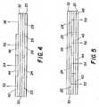
- Fig. 2an arrangement of four pixels 10 having red 12, green 14, blue 16 and white 18 light emitting elements as taught by Siwinski is shown. The light emitting elements in each pixel are arranged in a two by two array.
- the displaymay include an array of light emitting OLED pixels, each pixel having three or more gamut elements for emitting different colors of light specifying a gamut and at least one additional element for emitting a color of light within the gamut and wherein the power efficiency of the additional element is higher than the power efficiency of at least one of the three or more gamut elements; wherein all of the gamut elements for each color in the display are arranged in a first direction in a line such that no differently colored gamut element is in the line; wherein the colored gamut elements are arranged in a second direction orthogonal to the first direction in a line such that the colors of the gamut elements alternate in that line; and wherein the additional elements are arranged in lines in both the first and second directions.
- the advantages of this inventionare a color display device with improved power efficiency and compatibility with stripe pattern arrangements.
- an OLED displayincludes an array of light emitting OLED pixels 10, each pixel having three or more gamut elements such as red 12, green 14, blue 16 light emitting elements for emitting different colors of light specifying a gamut and at least one additional element such as white light emitting element 18 for emitting a color of light within the gamut.
- the power efficiency of the additional elementis higher than the power efficiency of the gamut elements so that by driving the additional element in place of the gamut elements, the power consumption of the display may reduced.
- All of the gamut elements for each color in the displayare arranged in a first direction Y in a line such that no differently colored gamut element is in the line.
- the colored gamut elementsare arranged in a second direction X orthogonal to the first direction in a line such that the colors of the gamut elements alternate in that line.
- This arrangement of light emitting elementsis compatible with text rendering software that requires stripe-pattern displays.
- the light emitting elements in the pixelsare all individually addressable using conventional means.
- luminance that would conventionally be produced by a combination of lower power efficiency gamut elementscan instead be produced by the higher power efficiency additional elements.
- any color that can be reproduced using the additional elementswill be more efficient than an equivalent reproduction using the gamut elements.
- a suitable transformation functionmay be provided by a signal processor that converts a standard color image signal to a power saving image signal that is employed to drive the display of the present invention.
- the present inventioncan be employed in most OLED device configurations that include four or more OLEDs per pixel. These include very unsophisticated structures comprising a separate anode and cathode per OLED to more sophisticated devices, such as passive matrix displays having orthogonal arrays of anodes and cathodes to form pixels, and active-matrix displays where each pixel is controlled independently, for example, with a thin film transistor (TFT).
- TFTthin film transistor
- a top-emitting OLED display having a plurality of light emitting elementsincludes a single layer of white light emitting material 30 formed on a substrate 20.
- a plurality of electrodes 22, 24, 26, and 28 separated by insulators 29define the light emitting elements 12, 14, 16 and 18 (see Fig. 1 ).
- a second transparent electrode 32is formed on the white-light emitting organic material 30.
- Red 42, green 44, blue 46 color filtersare provided over the electrodes 22, 24, and 26 respectively so that when white light is emitted from the organic layer 30, red light 52 is emitted above electrode 22, green light 54 is above electrode 24, and blue light 56 is above electrode 26. Unfiltered, white light 58 is emitted above electrode 28.
- a transparent encapsulating cover(not shown) is provided over the device.
- Alternative arrangements of the electrodes 22-28 and color filters 42-46may be provided as described below.
- an additional filter(not shown) may be supplied above the white emitter to adjust the white point of the light emitted from the additional light emitting elements.
- the second electrode 32need not be transparent while the first electrodes 22, 24, 26, and 28 are transparent.
- the color filters 42, 44, 46, and a white point adjusting filter 48are formed on the substrate 20 prior to forming the light emitting elements.
- the present inventionprovides compatibility with color stripe patterns preferred for rendering text.
- an example additional white elementis provided in sequence after the gamut elements.
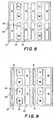
- a series of columns of each colorare composed of pixels 10 having color light emitting elements red 12, green 14, blue 16, and white 18.
- the elementsIn the vertical direction, the elements form a single colored striped line.
- the colored linesIn an orthogonal, horizontal direction, the colored lines alternate sequentially.
- the additional white light emitting elements 18are arranged to alternate with the green light emitting elements 14 so that the white and green elements are spatially symmetric, which may enhance the luminance resolution of the display since white and green both carry a relatively large amount of luminance information in a display.
- the white and green elements 18 and 14are arranged between the red and blue elements 12 and 16.
- the white element 18may also be placed between the green 14 and blue 16 elements (not shown).
- the additional element 18may be arranged with respect to the gamut elements to spatially integrate the light from the pixel 10.
- the additional element 18may be located beneath (or above) the gamut elements. Since the additional (in-gamut) element emits light that would otherwise be emitted from gamut elements, locating the additional element 18 such that its light emission is located near all the gamut elements will provide compatibility with a stripe arrangement and form a spatially integrated light source.
- a circuit pattern diagram for an active matrix display of the type shown in Fig. 7is shown.
- the light emitting elementsare connected to select lines 113, data lines 112a or 112b or 112c or 112d, power lines 111a , 111b or 111c , and capacitor lines 114.
- rows of light emitting elementsare selected by applying a voltage to a single select line, which turns on the select transistors 120 of the connected light emitting elements.
- the brightness level for each light emitting elementis controlled by a voltage signal, which is held on the data lines.
- the storage capacitor 130 of each selected elementis then charged to the voltage level of the associated data line 112a, 112b, 112c or 112d.
- the storage capacitoris connected to the gate of the power transistor 140 so that the voltage level held on the storage capacitor regulates the current flow through the power transistor 140 to the light emitting elements' organic EL element 11 and thereby brightness is controlled.
- Each rowis then un-selected by applying a voltage signal to the select line 113 which turns off the select transistor 120.
- the data line 112 voltagesare then set to the levels desired for the next row and the select line of the next row is turned on. This is repeated for every row of light emitting elements.
- the storage capacitors 130maintain the data voltage until the row is selected again during the next image frame.
- the power linesare typically connected to a common voltage level for all light emitting elements. As shown here, the light emitting elements 12, 14, and 16 are connected to a different select line than light emitting element 18. This means that the brightness level of light emitting element 18 is written at a different time than that of light emitting elements 12, 14, and 16. However, an alternate configuration where a pixel is defined as being composed of light emitting elements 18, 20e, 20f, and 20g, would result in the brightness level of all light emitting elements within the pixel being adjusted simultaneously and is understood to be within the scope of the invention.
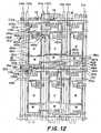
- Fig. 12shows a layout pattern diagram for the active matrix circuit of Fig. 11 as described above.
- the drive circuitry componentsare fabricated using conventional integrated circuit technologies.
- Light emitting element 12for example, consists of a select transistor 120a formed from a first semiconductor region 121a using techniques well known in the art.
- a power transistor 140ais formed in a second semiconductor region 141a.
- the first semiconductor region 121a and second semiconductor region 141aare typically formed in the same semiconductor layer.
- This semiconductor layeris typically silicon which may be amorphous, polycrystalline, or crystalline.
- This first semiconductor region 121aalso forms one side of the storage capacitor 130a.
- an insulating layer(not shown) that forms the gate insulator of the select transistor 120a, the gate insulator for power transistor 140a, and the insulating layer of the storage capacitor 130a.
- the gate of the select transistor 120ais formed from part of the select line 113a which is formed in the first conductive layer.
- the power transistor 140ahas a separate gate conductor 143a also preferably formed in the first conductive layer.
- the other electrode of the storage capacitor 130ais formed as part of capacitor line 114a, also preferably from the first conductive layer.
- the power line 111a and the data lines 112a respectively,are preferably formed in a second conductive layer.
- One or more of the signal linese.g. select line 113a
- the organic EL elementis formed by patterning a first electrode 181a for each pixel as well as depositing one or more layers of organic EL media (not shown) and a second electrode (not shown).
- Connections between layersare formed by etching holes (or vias) in the insulating layers such as the first via 122a connecting data line 112a, to the first semiconductor region 121a of the select transistor, the second via 142a connecting the power transistor gate conductor 143a to first semiconductor region 121a of the storage capacitor 130a and the select transistor 120a, the third via 146a connecting the second semiconductor region 141a of the power transistor to power line 111a, and the fourth via 145a connecting the second semiconductor region 141a of the power transistor to the first electrode 181a.
- an inter-element insulating filmis formed to reduce shorts between the anode and the cathode.
- Use of such insulating films over the first electrodeis disclosed in US 6,246,179 issued June 12, 2001 to Yamada .
- the inter-element insulating filmis coated over all the light emitting elements of the display and openings are made to allow the first electrodes to connect to the OLED layers (not shown).
- opening 191ais formed in the inter-pixel dielectric over the first electrode 181a. Opening 191a defines the area of the light emitting element which will emit light. While use of the inter-element insulating film is preferred, it is not required for successful implementation of the invention.
- Light emitting elements 14 and 16are formed similarly to light emitting element 12 and are connected to data lines 112b and 112c respectively as well as to power lines 111b and 112c respectively.
- Light emitting element 18is connected to select line 113b, capacitor line 114b, data line 112d, and power line 111c. Light emitting element 18 can alternately be connected to power line 111b or 111a or be provided a unique power line not shared by light emitting elements having other colors by someone skilled in the art.
- light emitting element 18consists of a select transistor 120b, a storage capacitor 130b, and power transistor 140b.
- the select transistor and capacitorare constructed with a first semiconductor region 121 b.
- the power transistoris constructed with a second semiconductor region 141b and a gate electrode 143b connected to the first semiconductor region by via 142b, to power line 111c by via 146b, and to the first electrode 181b by via 145b.
- first conductive bridge 150which is preferably constructed of the first conductive layer.
- the conductive bridgeis connected to data line 112d by via 151b and to the first semiconductor region by via 151a. While use of first conductive bridge 150 is preferred, it is not required, and other connection methods including connecting the first semiconductor region 121b directly to data line 112d can be achieved by someone skilled in the art. Furthermore, depending on how the data lines are arranged, the conductive bridge maybe applied to a light emitting element other than light emitting element 18.
- the conductive bridgemay be applied to light emitting element 12 instead of light emitting element 18.
- more than one conductive bridgemay be used to pass data lines on more than one light emitting element.
- Light emitting element 18also preferably uses a second conductive bridge 152 to connect the second capacitor electrode 131 to the capacitor line 114b bridging over the select line 113b .
- the second conductive bridge 152is preferably constructed in the second conductive layer.
- the second conductive bridge 152connects to the second capacitor electrode 131 by via 153b and to capacitor line 114b by via 153a .
- the second conductive bridgemay be located on a light emitting element (or more than one light emitting element) other than light emitting element 18. Variations of the light emitting elements can be constructed without a second conductive bridge if the select lines and capacitor lines are fabricated of different conductive layers.
- the first electrode 181b of light emitting element 18stretches across several signal lines such as power lines 111a and 111b as well as data lines 112b and 112c. These regions are not emitting in a bottom emission configuration and may be covered with inter-pixel dielectric. This results in three separate openings in the inter-element dielectric 191x, 191y, and 191z which results in three separate emitting regions for light emitting element 18.
- the light emitting elements of the present inventionhave been shown and have been described as configured in a bottom-emission configuration. If the device were to be configured in a top-emission configuration, the first electrodes can be increased in size and made to extend over the other various circuit components and signal lines. The openings in the inter-pixel dielectric can be increased in a similar fashion. In this case, the light emitting element 18 would not need to be provided multiple separate openings, and thereby multiple separate emitting regions, but could instead be provided one larger continuous opening and emitting region. Such a configuration is envisioned as being consistent with the present invention.
- a single gate transistorcontains a gate, a source and a drain.
- An example of the use of a single gate type of transistor for the select transistoris shown in US 6,429,599 issued August 6, 2002 to Yokoyama .
- a double transistorcontains at least two gates electrically connected together and therefore a source, a drain, and at least one intermediate source-drain between the gates.
- An example of the use of a multi-gate type of transistor for the select transistoris shown in US 6,476,419 , referenced above.
- This type of transistorcan be represented in a circuit schematic by a single transistor or two or more transistors in series which have their gates connected and the source of one transistor connected directly to the drain of the second transistor. While the performance of these transistor designs may differ, both types of transistors serve the same function in the circuit and either type can be applied to the present invention by someone skilled in the art.
- the example of the preferred embodiment of the present inventionis shown with a multi-gate type select transistor 120 represented by a single transistor symbol.
- multiple parallel transistorsto which is typically applied the power transistor 140.
- Multiple parallel transistorsare described in US 6,501,448 issued December 31, 2002 to Komiya et al. Multiple parallel transistors consist of two or more transistors with their sources, drains, and gates all electrically connected together. However, the location of the multiple transistors are separated in location within the pixels providing multiple parallel paths for current flow.
- the use of multiple parallel transistorshas the advantage of providing robustness against variability and defects in the semiconductor layer manufacturing process. While the power transistor described in the embodiments of the present invention are shown as a single transistor, this can be replaced by multiple parallel transistors by someone skilled in the art and are therefore understood to be within the scope of the invention.
- the drive circuitryis disposed over substrate 20 and under OLED layer 310 in a manner herein described.
- Layer 310includes a hole injecting layer 311, a hole transporting layer 312, a light emitting layer 313, and an electron transporting layer 314.
- a semiconductor layeris formed, doped, and patterned creating the second semiconductor region 141a.
- a gate insulating layer 212is formed over the semiconductor layer. Over the gate insulating layer 212, a gate conductor is formed in the first conductor layer. The semiconductor layer is then doped to form source and drain regions on either sides of the gate conductor 143a.
- a first interlayer insulator layer 213is formed over the gate conductor 143a. Over the first interlayer insulator layer 213, a second conductor layer is deposited and patterned forming the first power lines (e.g. 111a) and the data lines (e.g. 112a and 112d). A second interlayer insulator layer 214 is formed over the power and data lines (e.g. 111a, 112a, etc.). The first electrode 181a is formed over the second interlayer insulator layer 214. The first electrode 181a is patterned. Around the edges of the first electrode 181a, an inter element dielectric film 220 is formed to reduce shorts between the first electrode 181a and the second electrode 320.
- FIG. 14an alternate arrangement of the drive circuitry is shown.
- the arrangement of the data lines and power lineshas been configured such that there are two power lines 111a and 111b per pixel in a row.
- light emitting elements 14 and 18share power line 111a.
- Light emitting element 16shares a power line 111b with a light emitting element from an adjacent pixel. That is, light emitting element 14 is connected to a power line 111b of an adjacent pixel.
- This arrangementhas fewer power lines per pixel than the arrangement in Fig. 11 and each power line carries the current load from two light emitting elements.
- Fig. 15shows a layout pattern diagram for the active matrix circuit of Fig. 14 as described above. This pattern has the same transistor and capacitor components as described in Fig 12 .
- the first conductive bridge 154is connected to the first semiconductor region 121a of light emitting element 12 by via 155a and to a power line 111b by via 155b bridging over data line 112d.
- the second conductive bridge 152connects the second capacitor electrode 131 of light emitting element 18 to the capacitor line 114b bridging over the select line 113b.
- the third conductive bridge 156connects to the second semiconductor region 141b of light emitting element 18 by via 157b and to power line 111a by via 157a.
- conductive bridgesare shown as part of particular light emitting elements, they may be located on other light emitting elements other than those shown. While use of the conductive bridges is preferred, they are not required to successfully practice the present invention.
- FIG. 16an alternative arrangement of the pixel circuit of the first embodiment is shown.
- the arrangement of the data lines and power lines for two adjacent pixels 10 and 9have been configured such that there are three power lines 111a, 111b , and 111c for every two pixels in a row.
- light emitting elements 16, 18, 12b, and 18bare all connected to power line 111b.
- This arrangementhas fewer power lines per pixel than the arrangements in Fig. 11 and Fig. 14 .
- Fig. 17shows a layout pattern diagram for the active matrix circuit of Fig. 16 as described above. This pattern has the same transistor and capacitor components as described in the Fig 12 .
- the layout of light emitting elements 12b, 14b, 16b, and 18bare reversed with respect to light emitting elements 12,14,16, and 18.
- the power transistor 140c of light emitting element 16 and the power transistor 140i of light emitting element 12bare both connected to power line 111b. Therefore these transistors can be formed from the same semiconductor region 141c and contact can be made between the semiconductor region 141c and the power line 111b using the same via 146i.
- the power transistor 140d of light emitting element 18 and the power transistor 140L of light emitting element 18bare both connected to power line 111b. Therefore these transistors can be formed from the same semiconductor region 141d and contact can be made between the semiconductor region 141d and the power line 111b using the same via 146L. While using the same via and semiconductor region for the above-mentioned transistors is desirable, it is not required to successfully practice the invention.
- the white element 18is arranged near the center of the pixel 10.
- Each pixel 10includes the red 12, green 14, and blue 16 elements as conventionally arranged except that the center element 14 is smaller.
- the additional element 18is located below (or above) the center element. Since a white element effectively emits light that would otherwise be emitted from all three color elements, locating the white element 18 such that the white light emission is located near the center of all three color elements will provide compatibility with a stripe arrangement.
- a layout patternis shown where the white light emitting element 18 and the green light emitting element 14 are aligned into a single stripe as illustrated in Fig. 8 .
- Any of the circuit layout examples described abovecan be made to drive this arrangement.
- the example shown in Fig. 18shows a system with two power lines per pixel in a row. When arranged such that light emitting elements 14 and 18 form a stripe, only a single opening 190d in the inter-element dielectric layer is required for light emitting element 18.
- the displayis capable of presenting all of the colors presented by a standard three color, red, green, blue OLED display device.
- the color of the white OLED 18may be designed to match the white point of the display.
- the signal processor used to drive the displayis configured to allow any gray value, including white, which would typically be presented using a combination of the red 12, green 14, and blue 16 color OLEDs to be created using primarily the white OLED 18.
- the peak luminance of the white OLED 18is designed to match the combined luminance of the red 12, green 14, and blue 16 OLEDs. That is, in a typical configuration where the prior art display would be designed to achieve a peak luminance of 100 cd/sq. m, the red 12, green 14, and blue 16 OLEDs will be set up to produce this peak luminance when they are all turned on to their maximum value and the white OLED 18 will also be designed to provide this same peak luminance.
- the color of the additional element 18may be desirable to design the color of the additional element 18 to provide a color point other than the display white point inside the gamut defined by the red, green, and blue elements. For example by biasing the color of the additional or "white" element 18 towards the color of one of the gamut elements, the designer reduces the reliance of the display on gamut element toward which the additional element is biased.
- the peak luminance of the additional elementmay also be desirable to set the peak luminance of the additional element to other luminance values, including lower values, such as half the luminance of the peak luminance of the combined gamut elements which increases the reliance on the gamut elements while reducing the reliance on the additional element.
- the peak luminance of the additional elementmay also be designed to higher values, such as one and a half times the peak luminance of the combined gamut elements.
- this biascan result in loss of saturation for colors that are high in luminance that should be rendered as high in saturation.
- a suitable methodis employed to map from a conventional three-channel data signal to a four-channel signal, for example using a suitable look-up table.
- Methods of generating lookup tables for converting a three channel data signal to drive a display having four or more color channelsare well-known in the art, for example, US 6,075,514 issued June 13, 2000 to Ryan , provides one such method.
- the conversionmay be accomplished in real time using an algorithm that specifies the conversion.
- the transform from three to four colorsis nondeterministic, (i.e. many colors in the conventional specification can be created with either combinations of the gamut elements alone or in one of many combinations with the additional element), different conversions are possible.
- the peak luminance of the additional elementto match the combined peak luminances of the gamut elements, it is possible to perform the conversion to allow the additional element to provide as much luminance to each color as possible while maintaining saturation of all colors. This approach provides the maximum power savings possible with the present invention.
- a second particularly useful embodimentincludes the use of several different OLED materials that are doped to provide multiple colors.
- the red 12, green 14, blue 16 and white 18 OLEDsmay be composed of different OLED materials that are doped to produce different colored OLEDs.
- a different layer of organic light emitting diode materials 62-68respectively is formed.
- a second electrode 32is formed over the organic light emitting diode materials.
- Each of the organic light emitting diode materials(e.g., 62, 64,66 and 68 ) are formed from a hole injecting layer, a hole transporting layer, a light emitting layer, and an electron transporting layer as described in more detail below.
- the light emitting layer and potentially other layers within the stack of organic light emitting diode materialsare selected to provide a red, green, blue, and white light emitting elements.
- One light emitting diode material 62emits light primarily in the long wavelength or red portion of the visible spectrum.
- a second light emitting diode material 64emits light primarily in the middle wavelength or green portion of the visible spectrum.
- a third light emitting diode material 66emits light primarily in the short wavelength or blue portion of the visible spectrum.
- the fourth light emitting diode material 68emits light in a broad range of wavelengths, producing a white OLED. In this way, the four different materials form a four-OLED display including red, green, blue, and white OLEDs.
- OLEDs formed from materials that are doped to produce different colorsmay have significantly different luminance efficiencies and therefore it may be desirable to select a white OLED with chromaticity coordinates that are biased towards the chromaticity coordinate of the OLED with the lowest power efficiency.
- the chromaticity coordinate of the white OLEDin this way, the element with the lowest power efficiency is replaced more often by the white OLED, decreasing the overall power usage.
- the different OLEDsmay need to be driven at different levels to produce a color-balanced display. It is important to realize that the stability of OLED materials is inversely related to the current density that is used to drive the OLED. The lifetime of an OLED is influenced by the stability (i.e., the current density used to drive the OLED), therefore, the need to drive some elements with a higher current density may shorten the life of the OLEDs of the given color. Further, OLED materials that are doped to produce different colors typically have different luminance stabilities. That is, the change in luminance output that occurs over time is different for the different materials.
- a materialmay be employed for the white OLED having a chromaticity coordinate that is positioned closer to the OLED with the shortest luminance stability than to the chromaticity coordinates of the other gamut defining OLEDs. Positioning the white OLED according to this criteria reduces the overall usage of the closest gamut-defining OLED, extending the lifetime of the closest gamut-defining OLED.
- the additional elementis significantly more efficient than the gamut elements, the current density or power required to drive the additional element is significantly lower than for the gamut elements.
- the luminance stability over time of the materials used to create the light emitting elementsis typically related to the current density used to drive the elements through a very non-linear function in which the luminance stability over time of the material is much poorer when driven to higher current densities.
- the function used to describe this relationshipcan typically be described as a power function. For this reason, it is not desirable to drive any elements to current densities that are higher than a given threshold where the function describing the luminance stability over time is particularly steep. At the same time, it may be desirable to achieve maximum display luminance values that would typically require the gamut elements to be driven to this current density.
- the various light emitting elementswill have different efficiencies and lifetimes.
- the additional white OLED elementscan be increased in size.
- US 6,366,025 issued April 2, 2002 to Yamadadescribes an electro-luminescent color display device having red, green, and blue light emitting elements having different areas to take into consideration the differing emission efficiencies and luminance ratios of the light emitting elements. The concept described by Yamada can be applied to the display device of the present invention. Referring to Fig. 9 , a display having elements of varying areas depending on expected usage, efficiency and lifetime is shown.
- the inventionis employed in a device that includes Organic Light Emitting Diodes (OLEDs) which are composed of small molecule or polymeric OLEDs as disclosed in but not limited to US 4,769,292, issued September 6, 1988 to Tang et al. , and US 5,061,569, issued October 29, 1991 to VanSlyke et al. Many combinations and variations of organic light emitting displays can be used to fabricate such a device.
- OLEDsOrganic Light Emitting Diodes
- the present inventioncan be employed in most OLED device configurations. These include very simple structures comprising a single anode and cathode to more complex devices, such as passive matrix displays comprised of orthogonal arrays of anodes and cathodes to form pixels, and active-matrix displays where each pixel is controlled independently, for example, with thin film transistors (TFTs).
- TFTsthin film transistors
- a typical structureis shown in Fig. 19 and is comprised of a substrate 701, an anode 703, a hole-injecting layer 705, a hole-transporting layer 707, a light-emitting layer 709, an electron-transporting layer 711, and a cathode 713. These layers are described in detail below. Note that the substrate may alternatively be located adjacent to the cathode, or the substrate may actually constitute the anode or cathode.
- the organic layers between the anode and cathodearc conveniently referred to as the organic EL element.
- the total combined thickness of the organic layersis preferably less than 500 nm.
- the anode and cathode of the OLEDare connected to a voltage/current source 850 through electrical conductors 860.
- the OLEDis operated by applying a potential between the anode and cathode such that the anode is at a more positive potential than the cathode. Holes are injected into the organic EL element from the anode and electrons are injected into the organic EL element at the anode.
- Enhanced device stabilitycan sometimes be achieved when the OLED is operated in an AC mode where, for some time period in the cycle, the potential bias is reversed and no current flows.
- An example of an AC-driven OLEDis described in US 5,552,678 .
- the OLED device of this inventionis typically provided over a supporting substrate where either the cathode or anode can be in contact with the substrate.
- the electrode in contact with the substrateis conveniently referred to as the bottom electrode.
- the bottom electrodeis the anode, but this invention is not limited to that configuration.
- the substratecan either be transmissive or opaque. In the case wherein the substrate is transmissive, a reflective or light absorbing layer is used to reflect the light through the cover or to absorb the light, thereby improving the contrast of the display.
- Substratescan include, but are not limited to, glass, plastic, semiconductor materials, silicon, ceramics, and circuit board materials. Of course it is necessary to provide a light-transparent top electrode.
- anodeWhen EL emission is viewed through anode 703, the anode should be transparent or substantially transparent to the emission of interest.
- Common transparent anode materials used in this inventionare indium-tin oxide (ITO), indium-zinc oxide (IZO) and tin oxide, but other metal oxides can work including, but not limited to, aluminum- or indium-doped zinc oxide, magnesium-indium oxide, and nickel-tungsten oxide.
- metal nitridessuch as gallium nitride
- metal selenidessuch as zinc selenide
- metal sulfidessuch as zinc sulfide
- anodeFor applications where EL emission is viewed only through the cathode electrode, the transmissive characteristics of anode are immaterial and any conductive material can be used, transparent, opaque or reflective.
- Example conductors for this applicationinclude, but are not limited to, gold, iridium, molybdenum, palladium, and platinum.
- Typical anode materials, transmissive or otherwise,have a work function of 4.1 eV or greater. Desired anode materials are commonly deposited by any suitable means such as evaporation, sputtering, chemical vapor deposition, or electrochemical means.
- Anodescan be patterned using well-known photolithographic processes.
- anodesmay be polished prior to application of other layers to reduce surface roughness so as to minimize shorts or enhance reflectivity.
- hole-injecting layer 705between anode 703 and hole-transporting layer 707.
- the hole-injecting materialcan serve to improve the film formation property of subsequent organic layers and to facilitate injection of holes into the hole-transporting layer.
- Suitable materials for use in the hole-injecting layerinclude, but are not limited to, porphyrinic compounds as described in US 4,720,432 , plasma-deposited fluorocarbon polymers as described in US 6,208,075 , and some aromatic amines, for example, m-MTDATA (4,4',4"-tris[(3-methylphenyl)phenylamino]triphenylamine).
- Alternative hole-injecting materials reportedly useful in organic EL devicesare described in EP 0 891 121 A1 and EP 1 029 909 A1 .
- the hole-transporting layer 707contains at least one hole-transporting compound such as an aromatic tertiary amine, where the latter is understood to be a compound containing at least one trivalent nitrogen atom that is bonded only to carbon atoms, at least one of which is a member of an aromatic ring.
- the aromatic tertiary aminecan be an arylamine, such as a monoarylamine, diarylamine, triarylamine, or a polymeric arylamine. Exemplary monomeric triarylamines are illustrated by Klupfel et al. US 3,180,730 .
- Other suitable triarylamines substituted with one or more vinyl radicals and/or comprising at least one active hydrogen containing groupare disclosed by Brantley et al US 3,567,450 and 3,658,520 .
- a more preferred class of aromatic tertiary aminesare those which include at least two aromatic tertiary amine moieties as described in US 4,720,432 and 5,061,569 .
- the hole-transporting layercan be formed of a single or a mixture of aromatic tertiary amine compounds.
- Illustrative of useful aromatic tertiary aminesare the following:
- Another class of useful hole-transporting materialsincludes polycyclic aromatic compounds as described in EP 1 009 041 . Tertiary aromatic amines with more than two amine groups may be used including oligomeric materials.
- polymeric hole-transporting materialscan be used such as poly(N-vinylcarbazole) (PVK), polythiophenes, polypyrrole, polyaniline, and copolymers such as poly(3,4-ethylenedioxythiophene) / poly(4-styrenesulfonate) also called PEDOT/PSS.
- the light-emitting layer (LEL) 709 of the organic EL elementincludes a luminescent or fluorescent material where electroluminescence is produced as a result of electron-hole pair recombination in this region.
- the light-emitting layercan be comprised of a single material, but more commonly consists of a host material doped with a guest compound or compounds where light emission comes primarily from the dopant and can be of any color.
- the host materials in the light-emitting layercan be an electron-transporting material, as defined below, a hole-transporting material, as defined above, or another material or combination of materials that support hole-electron recombination.
- the dopantis usually chosen from highly fluorescent dyes, but phosphorescent compounds, e.g., transition metal complexes as described in WO 98/55561 , WO 00/18851 , WO 00/57676 , and WO 00/70655 are also useful. Dopants are typically coated as 0.01 to 10 % by weight into the host material. Polymeric materials such as polyfluorenes and polyvinylarylenes (e.g., poly(p-phenylenevinylene), PPV) can also be used as the host material. In this case, small molecule dopants can be molecularly dispersed into the polymeric host, or the dopant could be added by copolymerizing a minor constituent into the host polymer.
- phosphorescent compoundse.g., transition metal complexes as described in WO 98/55561 , WO 00/18851 , WO 00/57676 , and WO 00/70655 are also useful.
- bandgap potentialis defined as the energy difference between the highest occupied molecular orbital and the lowest unoccupied molecular orbital of the molecule.
- band gap of the dopantis smaller than that of the host material.
- phosphorescent emittersit is also important that the host triplet energy level of the host be high enough to enable energy transfer from host to dopant.
- Host and emitting molecules known to be of useinclude, but are not limited to, those disclosed in US 4,768,292 ; 5,141,671 ; 5,150,006 ; 5,151,629 ; 5,405,709 ; 5,484,922 ; 5,593,788 ; 5,645,948 ; 5,683,823 ; 5,755,999 ; 5,928,802 ; 5,935,720 ; 5,935,721 ; and 6,020,078 .
- oxine8-hydroxyquinoline
- oxine8-hydroxyquinoline
- oxine8-hydroxyquinoline
- useful host compoundscapable of supporting electroluminescence.
- useful chelated oxinoid compoundsare the following:
- useful host materialsinclude, but are not limited to: derivatives of anthracene, such as 9,10-di-(2-naphthyl)anthracene and derivatives thereof as described in US 5,935,721 , distyrylarylene derivatives as described in US 5,121,029 , and benzazole derivatives, for example, 2, 2', 2"-(1,3,5-phenylene)tris[1-phenyl-1H-benzimidazole].
- Carbazole derivativesare particularly useful hosts for phosphorescent emitters.
- Useful fluorescent dopantsinclude, but are not limited to, derivatives of anthracene, tetracene, xanthene, perylene, rubrene, coumarin, rhodamine, and quinacridone, dicyanomethylenepyran compounds, thiopyran compounds, polymethine compounds, pyrilium and thiapyrilium compounds, fluorene derivatives, periflanthene derivatives, indenoperylene derivatives, bis(azinyl)amine boron compounds, bis(azinyl)methane compounds, and carbostyryl compounds.
- Preferred thin film-forming materials for use in forming the electron-transporting layer 711 of the organic EL elements of this inventionare metal chelated oxinoid compounds, including chelates of oxine itself (also commonly referred to as 8-quinolinol or 8-hydroxyquinoline). Such compounds help to inject and transport electrons, exhibit high levels of performance, and are readily fabricated in the form of thin films. Exemplary oxinoid compounds were listed previously.
- electron-transporting materialsinclude various butadiene derivatives as disclosed in US 4,356,429 and various heterocyclic optical brighteners as described in US 4,539,507 .
- Benzazoles and triazinesare also useful electron-transporting materials.
- the cathode 113 used in this inventioncan be comprised of nearly any conductive material. Desirable materials have good film-forming properties to ensure good contact with the underlying organic layer, promote electron injection at low voltage, and have good stability. Useful cathode materials often contain a low work function metal ( ⁇ 4.0 eV) or metal alloy.
- One preferred cathode materialis comprised of a Mg:Ag alloy wherein the percentage of silver is in the range of 1 to 20 %, as described in US 4,885,221 .
- cathode materialsinclude bilayers comprising a thin electron-injection layer (EIL) in contact with the organic layer (e.g., ETL) which is capped with a thicker layer of a conductive metal.
- EILelectron-injection layer
- the EILpreferably includes a low work function metal or metal salt, and if so, the thicker capping layer does not need to have a low work function.
- One such cathodeis comprised of a thin layer of LiF followed by a thicker layer of Al as described in US 5,677,572 .
- Other useful cathode material setsinclude, but are not limited to, those disclosed in US 5,059,861 , 5,059,862 , and 6,140,763 .
- the cathodeWhen light emission is viewed through the cathode, the cathode must be transparent or nearly transparent. For such applications, metals must be thin or one must use transparent conductive oxides, or a combination of these materials.
- Optically transparent cathodeshave been described in more detail in US 4,885,211 , US 5,247,190 , JP 3,234,963 , US 5,703,436 , US 5,608,287 , US 5,837,391 , US 5,677,572 , US 5,776,622 , US 5,776,623 , US 5,714,838 , US 5,969,474 , US 5,739,545 , US 5,981,306 , US 6,137,223 , US 6,140,763 , US 6,172,459 , EP 1 076 368 , US 6,278,236 , and US 6,284,393 .
- Cathode materialsare typically deposited by evaporation, sputtering, or chemical vapor deposition. When needed, patterning can be achieved through many well known methods including, but not limited to, through-mask deposition, integral shadow masking, for example, as described in US 5,276,380 and EP 0 732 868 , laser ablation, and selective chemical vapor deposition.
- layers 709 and 711can optionally be collapsed into a single layer that serves the function of supporting both light emission and electron transportation. It also known in the art that emitting dopants may be added to the hole-transporting layer, which may serve as a host. Multiple dopants may be added to one or more layers in order to create a white-emitting OLED, for example, by combining blue- and yellow-emitting materials, cyan- and red-emitting materials, or red-, green-, and blue-emitting materials.
- White-emitting devicesare described, for example, in EP 1 187 235 , US 20020025419 , EP 1 182 244 , US 5,683,823 , US 5,503,910 , US 5,405,709 , and US 5,283,182 .
- Additional layerssuch as electron or hole-blocking layers as taught in the art may be employed in devices of this invention.
- Hole-blocking layersare commonly used to improve efficiency of phosphorescent emitter devices, for example, as in US 20020015859 .
- This inventionmay be used in so-called stacked device architecture, for example, as taught in US 5,703,436 and US 6,337,492 .
- the organic materials mentioned aboveare suitably deposited through a vapor-phase method such as sublimation, but can be deposited from a fluid, for example, from a solvent with an optional binder to improve film formation. If the material is a polymer, solvent deposition is useful but other methods can be used, such as sputtering or thermal transfer from a donor sheet.
- the material to be deposited by sublimationcan be vaporized from a sublimator "boat" often comprised of a tantalum material, e.g., as described in US 6,237,529 , or can be first coated onto a donor sheet and then sublimed in closer proximity to the substrate.
- Layers with a mixture of materialscan utilize separate sublimator boats or the materials can be pre-mixed and coated from a single boat or donor sheet. Patterned deposition can be achieved using shadow masks, integral shadow masks ( US 5,294,870 ), spatially-defined thermal dye transfer from a donor sheet ( US 5,688,551 , 5,851,709 and 6,066,357 ) and inkjet method ( US 6,066,357 ).
- OLED devicesare sensitive to moisture or oxygen, or both, so they are commonly sealed in an inert atmosphere such as nitrogen or argon, along with a desiccant such as alumina, bauxite, calcium sulfate, clays, silica gel, zeolites, alkaline metal oxides, alkaline earth metal oxides, sulfates, or metal halides and perchlorates.
- a desiccantsuch as alumina, bauxite, calcium sulfate, clays, silica gel, zeolites, alkaline metal oxides, alkaline earth metal oxides, sulfates, or metal halides and perchlorates.
- Methods for encapsulation and desiccationinclude, but are not limited to, those described in US 6,226,890 .
- barrier layerssuch as SiOx, Teflon, and alternating inorganic/polymeric layers are known in the art for encapsulation.
- OLED devices of this inventioncan employ various well-known optical effects in order to enhance its properties if desired. This includes optimizing layer thicknesses to yield maximum light transmission, providing dielectric mirror structures, replacing reflective electrodes with light-absorbing electrodes, providing anti glare or anti-reflection coatings over the display, providing a polarizing medium over the display, or providing colored, neutral density, or color conversion filters over the display. Filters, polarizers, and anti-glare or anti-reflection coatings may be specifically provided over the cover or an electrode protection layer beneath the cover.
Landscapes
- Engineering & Computer Science (AREA)
- Physics & Mathematics (AREA)
- Computer Hardware Design (AREA)
- General Physics & Mathematics (AREA)
- Theoretical Computer Science (AREA)
- Electroluminescent Light Sources (AREA)
- Devices For Indicating Variable Information By Combining Individual Elements (AREA)
Description
- The present invention relates to OLED color displays and, more particularly, to arrangements of light emitting elements in such OLED color displays.
US Patent Application No. 2002/0186214A1 by Siwinski et al., published December 12, 2002 , shows a method for saving power in an organic light emitting diode (OLED) display having pixels comprised of red, green, blue and white light emitting elements. The white light emitting elements are more efficient than the other colored light emitting elements and are employed to reduce the power requirements of the display.- While power efficiency is always desirable, it is particularly desirable in portable applications because an inefficient display limits the time the device can be used before the power source is recharged. In fact, for certain applications the rate of power consumption may be more important than any other display characteristic with the exception of visibility. Referring to
Fig. 2 , an arrangement of fourpixels 10 having red 12, green 14, blue 16 and white 18 light emitting elements as taught by Siwinski is shown. The light emitting elements in each pixel are arranged in a two by two array. - International patent application with
publication No. WO 00/11728 - Document
EP 1 573 817 is another closely related prior art document. - Widely used text rendering software such as Microsoft ClearType™ relies upon displays in which the colored elements of the display are arranged to form vertical stripes. Such arrangements are known in LCD displays that have pixels comprised of red, green, and blue light emitting elements. An example of such an arrangement is shown in
Fig. 3 , however this arrangement does not provide the power savings of the display device taught by Siwinski. - There is a need, therefore, for an improved full-color flat-panel OLED display having improved power efficiency while maintaining full-color reproduction and compatibility with a stripe-pattern arrangement.
- The need is met by providing a color OLED display according to
claim 1. The display may include an array of light emitting OLED pixels, each pixel having three or more gamut elements for emitting different colors of light specifying a gamut and at least one additional element for emitting a color of light within the gamut and wherein the power efficiency of the additional element is higher than the power efficiency of at least one of the three or more gamut elements; wherein all of the gamut elements for each color in the display are arranged in a first direction in a line such that no differently colored gamut element is in the line; wherein the colored gamut elements are arranged in a second direction orthogonal to the first direction in a line such that the colors of the gamut elements alternate in that line; and wherein the additional elements are arranged in lines in both the first and second directions. - The advantages of this invention are a color display device with improved power efficiency and compatibility with stripe pattern arrangements.
Fig. 1 is a schematic diagram of a portion of an OLED display illustrating an arrangement of light emitting elements;Fig. 2 is a schematic diagram of a portion of an OLED display having light emitting elements arranged according to the prior art;Fig. 3 is a schematic diagram of a portion of an OLED display having light emitting elements arranged according to the prior art;Fig. 4 is a side view of a portion of a top-emitting OLED display according to one embodiment of the present invention;Fig. 5 is a side view of a portion of a bottom-emitting OLED display according to one embodiment of the present invention;Fig. 6 is a schematic diagram of a portion of an OLED display illustrating an alternative arrangement of light emitting elements;Fig. 7 is a schematic diagram of a portion of an OLED display having light emitting elements arranged according to an embodiment of the present invention;Fig. 8 is a schematic diagram of a portion of an OLED display having light emitting elements arranged according to an alternative embodiment of the present invention;Fig. 9 is a schematic diagram of a portion of an OLED display having light emitting elements arranged according to another alternative embodiment of the present invention;Fig. 10 is a side view of a portion of a top-emitting OLED display according to another embodiment of the present invention;Fig. 11 is a circuit layout diagram of a portion of the pixel area of an OLED display of the type shown inFig. 7 ;Fig. 12 is a detailed layout diagram of a portion of the pixel area of an OLED display shown inFig. 11 ;Fig. 13 is a cross sectional diagram of one light emitting element in an OLED display;Fig. 14 is an alternative circuit layout diagram of a portion of the pixel area of an OLED display of the type shown inFig. 7 ;Fig. 15 is a more detailedlayout diagram of a portion of the pixel area of an OLED display shown inFig. 14 ;Fig. 16 is another alternative circuit layout diagram of a portion of the pixel area of an OLED display of the type shown inFig. 7 ;Fig. 17 is a more detailed layout diagram of a portion of the pixel area of an OLED display shown inFig. 16 ;Fig. 18 is another alternative layout diagram of a portion of the pixel area of an OLED display of the type shown inFig. 8 ; andFig. 19 is a schematic side view of an OLED light emitting element according to the prior art.- Referring to
Fig. 1 , an OLED display includes an array of light emittingOLED pixels 10, each pixel having three or more gamut elements such as red 12, green 14, blue 16 light emitting elements for emitting different colors of light specifying a gamut and at least one additional element such as whitelight emitting element 18 for emitting a color of light within the gamut. The power efficiency of the additional element is higher than the power efficiency of the gamut elements so that by driving the additional element in place of the gamut elements, the power consumption of the display may reduced. All of the gamut elements for each color in the display are arranged in a first direction Y in a line such that no differently colored gamut element is in the line. The colored gamut elements are arranged in a second direction X orthogonal to the first direction in a line such that the colors of the gamut elements alternate in that line. This arrangement of light emitting elements is compatible with text rendering software that requires stripe-pattern displays. The light emitting elements in the pixels are all individually addressable using conventional means. - According to the present invention, luminance that would conventionally be produced by a combination of lower power efficiency gamut elements can instead be produced by the higher power efficiency additional elements. Thus, any color that can be reproduced using the additional elements will be more efficient than an equivalent reproduction using the gamut elements. A suitable transformation function may be provided by a signal processor that converts a standard color image signal to a power saving image signal that is employed to drive the display of the present invention.
- The present invention can be employed in most OLED device configurations that include four or more OLEDs per pixel. These include very unsophisticated structures comprising a separate anode and cathode per OLED to more sophisticated devices, such as passive matrix displays having orthogonal arrays of anodes and cathodes to form pixels, and active-matrix displays where each pixel is controlled independently, for example, with a thin film transistor (TFT).
- Referring to
Fig. 4 , a top-emitting OLED display having a plurality of light emitting elements includes a single layer of whitelight emitting material 30 formed on asubstrate 20. A plurality ofelectrodes insulators 29 define thelight emitting elements Fig. 1 ). A secondtransparent electrode 32 is formed on the white-light emittingorganic material 30. Red42, green44, blue46 color filters are provided over theelectrodes organic layer 30,red light 52 is emitted aboveelectrode 22,green light 54 is aboveelectrode 24, andblue light 56 is aboveelectrode 26. Unfiltered,white light 58 is emitted aboveelectrode 28. A transparent encapsulating cover (not shown) is provided over the device. Alternative arrangements of the electrodes 22-28 and color filters 42-46 may be provided as described below. Moreover, an additional filter (not shown) may be supplied above the white emitter to adjust the white point of the light emitted from the additional light emitting elements. - Referring to
Fig. 5 , in a bottom-emitting arrangement, light is emitted through thesubstrate 20. In this arrangement, thesecond electrode 32 need not be transparent while thefirst electrodes color filters point adjusting filter 48 are formed on thesubstrate 20 prior to forming the light emitting elements. - The present invention provides compatibility with color stripe patterns preferred for rendering text.
- In a simple arrangement, as shown in
Fig. 1 , an example additional white element is provided in sequence after the gamut elements. Referring toFig. 1 , a series of columns of each color are composed ofpixels 10 having color light emitting elements red 12, green 14, blue 16, and white 18. In the vertical direction, the elements form a single colored striped line. In an orthogonal, horizontal direction, the colored lines alternate sequentially. It should be noted that the light emitting element arrangements shown in the example described inFig. 1 and in the embodiments described below can be reflected or rotated without changing their properties. - In the arrangement shown in
Fig. 1 , the additional whitelight emitting elements 18 are arranged to alternate with the greenlight emitting elements 14 so that the white and green elements are spatially symmetric, which may enhance the luminance resolution of the display since white and green both carry a relatively large amount of luminance information in a display. - Referring to
Fig. 6 , in a slightly different exemplary arrangement, the white andgreen elements blue elements white element 18 may also be placed between the green 14 and blue 16 elements (not shown). These two configurations have the advantage of positioning the additional white element more centrally within the pixel. Since white light is a combination of colors, positioning the white light element in a central position within the pixel may provide a viewer with an experience more consistent with the experience from a conventional stripe pattern. - Referring to
Fig. 7 , in an embodiment, theadditional element 18 may be arranged with respect to the gamut elements to spatially integrate the light from thepixel 10. For example, theadditional element 18 may be located beneath (or above) the gamut elements. Since the additional (in-gamut) element emits light that would otherwise be emitted from gamut elements, locating theadditional element 18 such that its light emission is located near all the gamut elements will provide compatibility with a stripe arrangement and form a spatially integrated light source. - Referring to
Fig. 11 , a circuit pattern diagram for an active matrix display of the type shown inFig. 7 is shown. The light emitting elements are connected to selectlines 113,data lines power lines 111a,111b or111c, andcapacitor lines 114. To operate the display, rows of light emitting elements are selected by applying a voltage to a single select line, which turns on theselect transistors 120 of the connected light emitting elements. The brightness level for each light emitting element is controlled by a voltage signal, which is held on the data lines. Thestorage capacitor 130 of each selected element is then charged to the voltage level of the associateddata line power transistor 140 so that the voltage level held on the storage capacitor regulates the current flow through thepower transistor 140 to the light emitting elements'organic EL element 11 and thereby brightness is controlled. Each row is then un-selected by applying a voltage signal to theselect line 113 which turns off theselect transistor 120. Thedata line 112 voltages are then set to the levels desired for the next row and the select line of the next row is turned on. This is repeated for every row of light emitting elements. Thestorage capacitors 130 maintain the data voltage until the row is selected again during the next image frame. - The power lines are typically connected to a common voltage level for all light emitting elements. As shown here, the
light emitting elements element 18. This means that the brightness level of light emittingelement 18 is written at a different time than that of light emittingelements elements Fig. 12 shows a layout pattern diagram for the active matrix circuit ofFig. 11 as described above. The drive circuitry components are fabricated using conventional integrated circuit technologies.Light emitting element 12, for example, consists of aselect transistor 120a formed from afirst semiconductor region 121a using techniques well known in the art. Similarly, apower transistor 140a is formed in asecond semiconductor region 141a. Thefirst semiconductor region 121a andsecond semiconductor region 141a are typically formed in the same semiconductor layer.- This semiconductor layer is typically silicon which may be amorphous, polycrystalline, or crystalline. This
first semiconductor region 121a also forms one side of the storage capacitor 130a. Over thefirst semiconductor region 121a andsecond semiconductor region 141a is an insulating layer (not shown) that forms the gate insulator of theselect transistor 120a, the gate insulator forpower transistor 140a, and the insulating layer of the storage capacitor 130a. The gate of theselect transistor 120a is formed from part of theselect line 113a which is formed in the first conductive layer. - The
power transistor 140a has aseparate gate conductor 143a also preferably formed in the first conductive layer. The other electrode of the storage capacitor 130a is formed as part of capacitor line 114a, also preferably from the first conductive layer. The power line 111a and thedata lines 112a respectively, are preferably formed in a second conductive layer. One or more of the signal lines (e.g.select line 113a) frequently cross at least one or more of the other signal lines (e.g. data line 112a), which requires these lines to be fabricated from multiple conductive layers with at least one interlayer insulating layer (not shown). The organic EL element is formed by patterning afirst electrode 181a for each pixel as well as depositing one or more layers of organic EL media (not shown) and a second electrode (not shown). - Connections between layers are formed by etching holes (or vias) in the insulating layers such as the first via122a connecting
data line 112a, to thefirst semiconductor region 121a of the select transistor, the second via142a connecting the powertransistor gate conductor 143a tofirst semiconductor region 121a of the storage capacitor130a and theselect transistor 120a, the third via146a connecting thesecond semiconductor region 141a of the power transistor to power line111a, and the fourth via145a connecting thesecond semiconductor region 141a of the power transistor to thefirst electrode 181a. - Over the first electrode, an inter-element insulating film is formed to reduce shorts between the anode and the cathode. Use of such insulating films over the first electrode is disclosed in
US 6,246,179 issued June 12, 2001 to Yamada . The inter-element insulating film is coated over all the light emitting elements of the display and openings are made to allow the first electrodes to connect to the OLED layers (not shown). For light emittingelement 12, opening191a is formed in the inter-pixel dielectric over thefirst electrode 181a. Opening191a defines the area of the light emitting element which will emit light. While use of the inter-element insulating film is preferred, it is not required for successful implementation of the invention. Light emitting elements element 12 and are connected todata lines power lines Light emitting element 18 is connected to selectline 113b,capacitor line 114b,data line 112d, and power line111c.Light emitting element 18 can alternately be connected topower line 111b or111a or be provided a unique power line not shared by light emitting elements having other colors by someone skilled in the art. Like light emittingelement 12, light emittingelement 18 consists of aselect transistor 120b, astorage capacitor 130b, andpower transistor 140b. The select transistor and capacitor are constructed with afirst semiconductor region 121 b. The power transistor is constructed with asecond semiconductor region 141b and agate electrode 143b connected to the first semiconductor region by via142b, to power line111c by via146b, and to thefirst electrode 181b by via145b.- For light emitting
element 18, in order to connect thefirst semiconductor region 121b todata line 112d,data line 112a must be crossed. This is done using firstconductive bridge 150 which is preferably constructed of the first conductive layer. The conductive bridge is connected todata line 112d by via151b and to the first semiconductor region by via151a. While use of firstconductive bridge 150 is preferred, it is not required, and other connection methods including connecting thefirst semiconductor region 121b directly todata line 112d can be achieved by someone skilled in the art. Furthermore, depending on how the data lines are arranged, the conductive bridge maybe applied to a light emitting element other than light emittingelement 18. For example, if the locations ofdata line 112a anddata line 112d were reversed, then the conductive bridge may be applied to light emittingelement 12 instead of light emittingelement 18. Furthermore, more than one conductive bridge may be used to pass data lines on more than one light emitting element. Light emitting element 18 also preferably uses a secondconductive bridge 152 to connect thesecond capacitor electrode 131 to thecapacitor line 114b bridging over theselect line 113b. The secondconductive bridge 152 is preferably constructed in the second conductive layer. The secondconductive bridge 152 connects to thesecond capacitor electrode 131 by via153b and tocapacitor line 114b by via153a. As with the firstconductive bridge 150, by rearranging the components and connection lines, the second conductive bridge may be located on a light emitting element (or more than one light emitting element) other than light emittingelement 18. Variations of the light emitting elements can be constructed without a second conductive bridge if the select lines and capacitor lines are fabricated of different conductive layers.- The
first electrode 181b of light emittingelement 18 stretches across several signal lines such aspower lines 111a and111b as well asdata lines element 18. - The light emitting elements of the present invention have been shown and have been described as configured in a bottom-emission configuration. If the device were to be configured in a top-emission configuration, the first electrodes can be increased in size and made to extend over the other various circuit components and signal lines. The openings in the inter-pixel dielectric can be increased in a similar fashion. In this case, the
light emitting element 18 would not need to be provided multiple separate openings, and thereby multiple separate emitting regions, but could instead be provided one larger continuous opening and emitting region. Such a configuration is envisioned as being consistent with the present invention. - While the above embodiments have been described with reference to a specific configuration of the active matrix circuit, several variations of the conventional circuit which are known in the art can also be applied to the present invention by someone skilled in the art. For example, one variation such as that shown in
US 5,550,066 issued August 27, 1996 to Tang et al. does not have a separate capacitor line but instead connects the capacitors directly to the power line. A second variation as shown inUS 6,476,419 issued November 5, 2002 to Yasuda uses two capacitors disposed directly over each other where the first capacitor is fabricated between the semiconductor layer and the gate conductor layer and the second capacitor is fabricated between the gate conductor layer and the second conductor layer. Either of these variations can be applied to the present invention by someone skilled in the art. - While the circuit requires a select transistor and a power transistor for each light emitting element, several variations of these transistor designs are known in the art. For example, single and multi-gate versions of transistors are known and have been applied to the select transistors in prior art. A single gate transistor contains a gate, a source and a drain. An example of the use of a single gate type of transistor for the select transistor is shown in
US 6,429,599 issued August 6, 2002 to Yokoyama . A double transistor contains at least two gates electrically connected together and therefore a source, a drain, and at least one intermediate source-drain between the gates. An example of the use of a multi-gate type of transistor for the select transistor is shown inUS 6,476,419 , referenced above. This type of transistor can be represented in a circuit schematic by a single transistor or two or more transistors in series which have their gates connected and the source of one transistor connected directly to the drain of the second transistor. While the performance of these transistor designs may differ, both types of transistors serve the same function in the circuit and either type can be applied to the present invention by someone skilled in the art. The example of the preferred embodiment of the present invention is shown with a multi-gate typeselect transistor 120 represented by a single transistor symbol. - Also known in the art is the use of multiple parallel transistors to which is typically applied the
power transistor 140. Multiple parallel transistors are described inUS 6,501,448 issued December 31, 2002 to Komiya et al. Multiple parallel transistors consist of two or more transistors with their sources, drains, and gates all electrically connected together. However, the location of the multiple transistors are separated in location within the pixels providing multiple parallel paths for current flow. The use of multiple parallel transistors has the advantage of providing robustness against variability and defects in the semiconductor layer manufacturing process. While the power transistor described in the embodiments of the present invention are shown as a single transistor, this can be replaced by multiple parallel transistors by someone skilled in the art and are therefore understood to be within the scope of the invention. - Alternate circuit types are also known in the art such as constant current source driving schemes. An example of a constant current source device is provided in
US 6,501,466 issued December 31, 2002 to Yamagishi et al. - Alternate circuit types can be applied to the present invention by someone skilled in the art.
- Turning now to
Fig. 13 , the vertical arrangement of the various layers fromFig. 12 are shown. The drive circuitry is disposed oversubstrate 20 and underOLED layer 310 in a manner herein described.Layer 310 includes ahole injecting layer 311, ahole transporting layer 312, alight emitting layer 313, and anelectron transporting layer 314. Over thesubstrate 20, a semiconductor layer is formed, doped, and patterned creating thesecond semiconductor region 141a. Agate insulating layer 212 is formed over the semiconductor layer. Over thegate insulating layer 212, a gate conductor is formed in the first conductor layer. The semiconductor layer is then doped to form source and drain regions on either sides of thegate conductor 143a. A firstinterlayer insulator layer 213 is formed over thegate conductor 143a. Over the firstinterlayer insulator layer 213, a second conductor layer is deposited and patterned forming the first power lines (e.g. 111a) and the data lines (e.g. 112a and 112d). A secondinterlayer insulator layer 214 is formed over the power and data lines (e.g. 111a, 112a, etc.). Thefirst electrode 181a is formed over the secondinterlayer insulator layer 214. Thefirst electrode 181a is patterned. Around the edges of thefirst electrode 181a, an inter elementdielectric film 220 is formed to reduce shorts between thefirst electrode 181a and thesecond electrode 320. - Referring to
Fig. 14 , an alternate arrangement of the drive circuitry is shown. InFig. 14 , the arrangement of the data lines and power lines has been configured such that there are twopower lines 111a and 111b per pixel in a row. In this example,light emitting elements Light emitting element 16 shares apower line 111b with a light emitting element from an adjacent pixel. That is, light emittingelement 14 is connected to apower line 111b of an adjacent pixel. This arrangement has fewer power lines per pixel than the arrangement inFig. 11 and each power line carries the current load from two light emitting elements. Fig. 15 shows a layout pattern diagram for the active matrix circuit ofFig. 14 as described above. This pattern has the same transistor and capacitor components as described inFig 12 . In order to achieve the desired two power lines per pixel, several conductive bridge structures are utilized as described above. The first conductive bridge154 is connected to thefirst semiconductor region 121a of light emittingelement 12 by via155a and to apower line 111b by via155b bridging overdata line 112d. The secondconductive bridge 152 connects thesecond capacitor electrode 131 of light emittingelement 18 to thecapacitor line 114b bridging over theselect line 113b. The thirdconductive bridge 156 connects to thesecond semiconductor region 141b of light emittingelement 18 by via157b and to power line111a by via157a.- While these conductive bridges are shown as part of particular light emitting elements, they may be located on other light emitting elements other than those shown. While use of the conductive bridges is preferred, they are not required to successfully practice the present invention.
- Referring now to
Fig. 16 , an alternative arrangement of the pixel circuit of the first embodiment is shown. InFig. 16 , the arrangement of the data lines and power lines for twoadjacent pixels 10 and9 have been configured such that there are threepower lines 111a, 111b, and111c for every two pixels in a row. In this example,light emitting elements power line 111b. This arrangement has fewer power lines per pixel than the arrangements inFig. 11 andFig. 14 . Fig. 17 shows a layout pattern diagram for the active matrix circuit ofFig. 16 as described above. This pattern has the same transistor and capacitor components as described in theFig 12 . In order to achieve the desired three power lines per two pixels, the layout oflight emitting elements elements power transistor 140c of light emittingelement 16 and thepower transistor 140i of light emittingelement 12b are both connected topower line 111b. Therefore these transistors can be formed from thesame semiconductor region 141c and contact can be made between thesemiconductor region 141c and thepower line 111b using the same via146i. Similarly, thepower transistor 140d of light emittingelement 18 and the power transistor140L of light emittingelement 18b are both connected topower line 111b. Therefore these transistors can be formed from the same semiconductor region141d and contact can be made between the semiconductor region141d and thepower line 111b using the same via146L. While using the same via and semiconductor region for the above-mentioned transistors is desirable, it is not required to successfully practice the invention.- Referring to
Fig. 8 , in an alternative embodiment, thewhite element 18 is arranged near the center of thepixel 10. Eachpixel 10 includes the red12, green14, and blue16 elements as conventionally arranged except that thecenter element 14 is smaller. Theadditional element 18 is located below (or above) the center element. Since a white element effectively emits light that would otherwise be emitted from all three color elements, locating thewhite element 18 such that the white light emission is located near the center of all three color elements will provide compatibility with a stripe arrangement. - Referring to
Fig. 18 , a layout pattern is shown where the whitelight emitting element 18 and the greenlight emitting element 14 are aligned into a single stripe as illustrated inFig. 8 . Any of the circuit layout examples described above can be made to drive this arrangement. The example shown inFig. 18 shows a system with two power lines per pixel in a row. When arranged such thatlight emitting elements single opening 190d in the inter-element dielectric layer is required for light emittingelement 18. - The display is capable of presenting all of the colors presented by a standard three color, red, green, blue OLED display device. The color of the
white OLED 18 may be designed to match the white point of the display. In this embodiment, the signal processor used to drive the display is configured to allow any gray value, including white, which would typically be presented using a combination of the red12, green14, and blue16 color OLEDs to be created using primarily thewhite OLED 18. To achieve this, the peak luminance of thewhite OLED 18 is designed to match the combined luminance of the red12, green14, and blue16 OLEDs. That is, in a typical configuration where the prior art display would be designed to achieve a peak luminance of 100 cd/sq. m, the red12, green14, and blue 16 OLEDs will be set up to produce this peak luminance when they are all turned on to their maximum value and thewhite OLED 18 will also be designed to provide this same peak luminance. - It should be noted however, that under certain circumstances it may be desirable to design the color of the
additional element 18 to provide a color point other than the display white point inside the gamut defined by the red, green, and blue elements. For example by biasing the color of the additional or "white"element 18 towards the color of one of the gamut elements, the designer reduces the reliance of the display on gamut element toward which the additional element is biased. - It may also be desirable to set the peak luminance of the additional element to other luminance values, including lower values, such as half the luminance of the peak luminance of the combined gamut elements which increases the reliance on the gamut elements while reducing the reliance on the additional element. The peak luminance of the additional element may also be designed to higher values, such as one and a half times the peak luminance of the combined gamut elements. However, this bias can result in loss of saturation for colors that are high in luminance that should be rendered as high in saturation.
- Once the display is designed to provide the correct luminance value for each element, a suitable method is employed to map from a conventional three-channel data signal to a four-channel signal, for example using a suitable look-up table. Methods of generating lookup tables for converting a three channel data signal to drive a display having four or more color channels are well-known in the art, for example,
US 6,075,514 issued June 13, 2000 to Ryan , provides one such method. Alternatively, the conversion may be accomplished in real time using an algorithm that specifies the conversion. - Because the transform from three to four colors is nondeterministic, (i.e. many colors in the conventional specification can be created with either combinations of the gamut elements alone or in one of many combinations with the additional element), different conversions are possible. However, by selecting the peak luminance of the additional element to match the combined peak luminances of the gamut elements, it is possible to perform the conversion to allow the additional element to provide as much luminance to each color as possible while maintaining saturation of all colors. This approach provides the maximum power savings possible with the present invention.
- Various other embodiments of this invention may also be practiced. A second particularly useful embodiment includes the use of several different OLED materials that are doped to provide multiple colors. For example, the red12, green14, blue16 and white18 OLEDs may be composed of different OLED materials that are doped to produce different colored OLEDs. Referring to
Fig. 10 , in this embodiment, on each first electrode22-28 a different layer of organic light emitting diode materials62-68 respectively is formed. Over the organic light emitting diode materials asecond electrode 32 is formed. Each of the organic light emitting diode materials (e.g.,62, 64,66 and68) are formed from a hole injecting layer, a hole transporting layer, a light emitting layer, and an electron transporting layer as described in more detail below. - In this embodiment, the light emitting layer and potentially other layers within the stack of organic light emitting diode materials are selected to provide a red, green, blue, and white light emitting elements. One light emitting
diode material 62 emits light primarily in the long wavelength or red portion of the visible spectrum. A second light emittingdiode material 64 emits light primarily in the middle wavelength or green portion of the visible spectrum. A third light emittingdiode material 66 emits light primarily in the short wavelength or blue portion of the visible spectrum. Finally, the fourth light emittingdiode material 68 emits light in a broad range of wavelengths, producing a white OLED. In this way, the four different materials form a four-OLED display including red, green, blue, and white OLEDs. - In this implementation, OLEDs formed from materials that are doped to produce different colors may have significantly different luminance efficiencies and therefore it may be desirable to select a white OLED with chromaticity coordinates that are biased towards the chromaticity coordinate of the OLED with the lowest power efficiency. By selecting the chromaticity coordinate of the white OLED in this way, the element with the lowest power efficiency is replaced more often by the white OLED, decreasing the overall power usage.
- Further, within this implementation, the different OLEDs may need to be driven at different levels to produce a color-balanced display. It is important to realize that the stability of OLED materials is inversely related to the current density that is used to drive the OLED. The lifetime of an OLED is influenced by the stability (i.e., the current density used to drive the OLED), therefore, the need to drive some elements with a higher current density may shorten the life of the OLEDs of the given color. Further, OLED materials that are doped to produce different colors typically have different luminance stabilities. That is, the change in luminance output that occurs over time is different for the different materials. To account for this, a material may be employed for the white OLED having a chromaticity coordinate that is positioned closer to the OLED with the shortest luminance stability than to the chromaticity coordinates of the other gamut defining OLEDs. Positioning the white OLED according to this criteria reduces the overall usage of the closest gamut-defining OLED, extending the lifetime of the closest gamut-defining OLED.
- In the embodiments that have been discussed above, it is important to note that because the additional element is significantly more efficient than the gamut elements, the current density or power required to drive the additional element is significantly lower than for the gamut elements. It is also important to note that the luminance stability over time of the materials used to create the light emitting elements is typically related to the current density used to drive the elements through a very non-linear function in which the luminance stability over time of the material is much poorer when driven to higher current densities. In fact, the function used to describe this relationship can typically be described as a power function. For this reason, it is not desirable to drive any elements to current densities that are higher than a given threshold where the function describing the luminance stability over time is particularly steep. At the same time, it may be desirable to achieve maximum display luminance values that would typically require the gamut elements to be driven to this current density.
- In the embodiments described thus far, the various light emitting elements will have different efficiencies and lifetimes. To optimize a display device for various applications it is useful to use different sized elements. For example, in applications for which black-and-white use dominates, the additional white OLED elements can be increased in size. It should also be recognized that as the amount of luminance that is dedicated to the additional element is manipulated, it may also be desirable to change their relative sizes.
US 6,366,025 issued April 2, 2002 to Yamada , describes an electro-luminescent color display device having red, green, and blue light emitting elements having different areas to take into consideration the differing emission efficiencies and luminance ratios of the light emitting elements. The concept described by Yamada can be applied to the display device of the present invention. Referring toFig. 9 , a display having elements of varying areas depending on expected usage, efficiency and lifetime is shown. - In a preferred example, the invention is employed in a device that includes Organic Light Emitting Diodes (OLEDs) which are composed of small molecule or polymeric OLEDs as disclosed in but not limited to
US 4,769,292, issued September 6, 1988 to Tang et al. , andUS 5,061,569, issued October 29, 1991 to VanSlyke et al. Many combinations and variations of organic light emitting displays can be used to fabricate such a device. - The present invention can be employed in most OLED device configurations. These include very simple structures comprising a single anode and cathode to more complex devices, such as passive matrix displays comprised of orthogonal arrays of anodes and cathodes to form pixels, and active-matrix displays where each pixel is controlled independently, for example, with thin film transistors (TFTs).
- There are numerous configurations of the organic layers wherein the present invention can be successfully practiced. A typical structure is shown in
Fig. 19 and is comprised of a substrate701, ananode 703, a hole-injectinglayer 705, a hole-transportinglayer 707, a light-emitting layer709, an electron-transporting layer711, and acathode 713. These layers are described in detail below. Note that the substrate may alternatively be located adjacent to the cathode, or the substrate may actually constitute the anode or cathode. The organic layers between the anode and cathode arc conveniently referred to as the organic EL element. The total combined thickness of the organic layers is preferably less than 500 nm. - The anode and cathode of the OLED are connected to a voltage/
current source 850 throughelectrical conductors 860. The OLED is operated by applying a potential between the anode and cathode such that the anode is at a more positive potential than the cathode. Holes are injected into the organic EL element from the anode and electrons are injected into the organic EL element at the anode. Enhanced device stability can sometimes be achieved when the OLED is operated in an AC mode where, for some time period in the cycle, the potential bias is reversed and no current flows. An example of an AC-driven OLED is described inUS 5,552,678 . - The OLED device of this invention is typically provided over a supporting substrate where either the cathode or anode can be in contact with the substrate. The electrode in contact with the substrate is conveniently referred to as the bottom electrode. Conventionally, the bottom electrode is the anode, but this invention is not limited to that configuration. The substrate can either be transmissive or opaque. In the case wherein the substrate is transmissive, a reflective or light absorbing layer is used to reflect the light through the cover or to absorb the light, thereby improving the contrast of the display. Substrates can include, but are not limited to, glass, plastic, semiconductor materials, silicon, ceramics, and circuit board materials. Of course it is necessary to provide a light-transparent top electrode.
- When EL emission is viewed through
anode 703, the anode should be transparent or substantially transparent to the emission of interest. Common transparent anode materials used in this invention are indium-tin oxide (ITO), indium-zinc oxide (IZO) and tin oxide, but other metal oxides can work including, but not limited to, aluminum- or indium-doped zinc oxide, magnesium-indium oxide, and nickel-tungsten oxide. In addition to these oxides, metal nitrides, such as gallium nitride, and metal selenides, such as zinc selenide, and metal sulfides, such as zinc sulfide, can be used as the anode. For applications where EL emission is viewed only through the cathode electrode, the transmissive characteristics of anode are immaterial and any conductive material can be used, transparent, opaque or reflective. Example conductors for this application include, but are not limited to, gold, iridium, molybdenum, palladium, and platinum. Typical anode materials, transmissive or otherwise, have a work function of 4.1 eV or greater. Desired anode materials are commonly deposited by any suitable means such as evaporation, sputtering, chemical vapor deposition, or electrochemical means. Anodes can be patterned using well-known photolithographic processes. Optionally, anodes may be polished prior to application of other layers to reduce surface roughness so as to minimize shorts or enhance reflectivity. - While not always necessary, it is often useful to provide a hole-injecting
layer 705 betweenanode 703 and hole-transportinglayer 707. The hole-injecting material can serve to improve the film formation property of subsequent organic layers and to facilitate injection of holes into the hole-transporting layer. Suitable materials for use in the hole-injecting layer include, but are not limited to, porphyrinic compounds as described inUS 4,720,432 , plasma-deposited fluorocarbon polymers as described inUS 6,208,075 , and some aromatic amines, for example, m-MTDATA (4,4',4"-tris[(3-methylphenyl)phenylamino]triphenylamine). Alternative hole-injecting materials reportedly useful in organic EL devices are described inEP 0 891 121 A1 andEP 1 029 909 A1 - The hole-transporting
layer 707 contains at least one hole-transporting compound such as an aromatic tertiary amine, where the latter is understood to be a compound containing at least one trivalent nitrogen atom that is bonded only to carbon atoms, at least one of which is a member of an aromatic ring. In one form the aromatic tertiary amine can be an arylamine, such as a monoarylamine, diarylamine, triarylamine, or a polymeric arylamine. Exemplary monomeric triarylamines are illustrated byKlupfel et al. US 3,180,730 . Other suitable triarylamines substituted with one or more vinyl radicals and/or comprising at least one active hydrogen containing group are disclosed byBrantley et al US 3,567,450 and3,658,520 . - A more preferred class of aromatic tertiary amines are those which include at least two aromatic tertiary amine moieties as described in
US 4,720,432 and5,061,569 . The hole-transporting layer can be formed of a single or a mixture of aromatic tertiary amine compounds. Illustrative of useful aromatic tertiary amines are the following: - 1,1-Bis(4-di-p-tolylaminophenyl)cyclohexane
- 1,1-Bis(4-di-p-tolylaminophenyl)-4-phenylcyclohexane
- 4,4'-Bis(diphenylamino)quadriphenyl
- Bis(4-dimethylamino-2-methylphenyl)-phenylmefhane
- N,N,N-Tri(p-tolyl)amine
- 4-(di-p-tolylamino)-4'-[4(di-p-tolylamino)-styryl]stilbene
- N,N,N',N'-Tetra-p-tolyl-4-4'-diaminobiphenyl
- N,N,N',N'-Tetraphenyl-4,4'-diaminobiphenyl
- N,N,N',N'-tetra-1-naphthyl-4,4'-diaminobiphenyl
- N,N,N',N'-tetra-2-naphthyl-4,4'-diaminobiphenyl
- N-Phenylcarbazole
- 4,4'-Bis[N-(1-naphthyl)-N-phenylamino]biphenyl
- 4,4'-Bis[N-(1-naphthyl)-N-(2-naphthyl)amino]biphenyl
- 4,4"-Bis[N-(1-naphthyl)-N-phenylamino]p-terphenyl
- 4,4'-Bis[N-(2-naphthyl)-N-phenylamino]biphenyl
- 4,4-Bis[N-(3-acenaphthenyl)-N-phenylamino]biphenyl
- 1,5-Bis[N-(1-naphthyl)-N-phenylamino]naphthalene
- 4,4'-Bis[N-(9-anthryl)-N-phenylamino]biphenyl
- 4,4"-Bis[N-(1-anthryl)-N-phenylamino]-p-terphenyl
- 4,4'-Bis[N-(2-phenanthryl)-N-phenylamino]biphenyl
- 4,4'-Bis[N-(8-fluoranthenyl)-N-phenylamino]biphenyl
- 4,4'-Bis[N-(2-pyrenyl)-N-phenylamino]biphenyl
- 4,4'-Bis[N-(2-naphthacenyl)-N-phenylamino]biphenyl
- 4,4'-Bis[N-(2-perylenyl)-N-phenylamino]biphenyl
- 4,4'-Bis[N-(1-coronenyl)-N-phenylamino]biphenyl
- 2,6-Bis(di-p-tolylamino)naphthalene
- 2,6-Bis[di-(1-naphthyl)amino]naphthalene
- 2,6-Bis[N-(1-naphthyl)-N-(2-naphthyl)amino]naphthalene
- N,N,N',N'-Tetra(2-naphthyl)-4,4"-diamino-p-terphenyl
- 4,4'-Bis{N-phenyl-N-[4-(1-naphthyl)-phenyl]amino}biphenyl
- 4,4'-Bis[N-phenyl-N-(2-pyrenyl)amino]biphenyl
- 2,6-Bis[N,N-di(2-naphthyl)amine]fluorene
- 1,5-Bis[N-(1-naphthyl)-N-phenylamino]naphthalene
- 4,4',4"-tris[(3-methylphenyl)phenylamino]triphenylamine
- Another class of useful hole-transporting materials includes polycyclic aromatic compounds as described in
EP 1 009 041 - As more fully described in
US 4,769,292 and5,935,721 , the light-emitting layer (LEL) 709 of the organic EL element includes a luminescent or fluorescent material where electroluminescence is produced as a result of electron-hole pair recombination in this region. The light-emitting layer can be comprised of a single material, but more commonly consists of a host material doped with a guest compound or compounds where light emission comes primarily from the dopant and can be of any color. The host materials in the light-emitting layer can be an electron-transporting material, as defined below, a hole-transporting material, as defined above, or another material or combination of materials that support hole-electron recombination. The dopant is usually chosen from highly fluorescent dyes, but phosphorescent compounds, e.g., transition metal complexes as described inWO 98/55561 WO 00/18851 WO 00/57676 WO 00/70655 - An important relationship for choosing a dye as a dopant is a comparison of the bandgap potential which is defined as the energy difference between the highest occupied molecular orbital and the lowest unoccupied molecular orbital of the molecule. For efficient energy transfer from the host to the dopant molecule, a necessary condition is that the band gap of the dopant is smaller than that of the host material. For phosphorescent emitters it is also important that the host triplet energy level of the host be high enough to enable energy transfer from host to dopant.
- Metal complexes of 8-hydroxyquinoline (oxine) and similar derivatives constitute one class of useful host compounds capable of supporting electroluminescence. Illustrative of useful chelated oxinoid compounds are the following:
- CO-1: Aluminum trisoxine [alias, tris(8-quinolinolato)aluminum(III)]
- CO-2: Magnesium bisoxine [alias, bis(8-quinolinolato)magnesium(II)]
- CO-3: Bis[benzo{f}-8-quinolinolato]zinc (II)
- CO-4: Bis(2-methyl-8-quinolinolato)aluminum(III)-□-oxo-bis(2-methyl-8-quinolinolato) aluminum(III)
- CO-5: Indium trisoxine [alias, tris(8-quinolinolato)indium]
- CO-6: Aluminum tris(5-methyloxine) [alias, tris(5-methyl-8-quinolinolato) aluminum(III)]
- CO-7: Lithium oxine [alias, (8-quinolinolato)lithium(I)]
- CO-8: Gallium oxine [alias, tris(8-quinolinolato)gallium(III)]
- CO-9: Zirconium oxine [alias, tetra(8-quinolinolato)zirconium(IV)]
- Other classes of useful host materials include, but are not limited to: derivatives of anthracene, such as 9,10-di-(2-naphthyl)anthracene and derivatives thereof as described in
US 5,935,721 , distyrylarylene derivatives as described inUS 5,121,029 , and benzazole derivatives, for example, 2, 2', 2"-(1,3,5-phenylene)tris[1-phenyl-1H-benzimidazole]. Carbazole derivatives are particularly useful hosts for phosphorescent emitters. - Useful fluorescent dopants include, but are not limited to, derivatives of anthracene, tetracene, xanthene, perylene, rubrene, coumarin, rhodamine, and quinacridone, dicyanomethylenepyran compounds, thiopyran compounds, polymethine compounds, pyrilium and thiapyrilium compounds, fluorene derivatives, periflanthene derivatives, indenoperylene derivatives, bis(azinyl)amine boron compounds, bis(azinyl)methane compounds, and carbostyryl compounds.
- Preferred thin film-forming materials for use in forming the electron-transporting layer 711 of the organic EL elements of this invention are metal chelated oxinoid compounds, including chelates of oxine itself (also commonly referred to as 8-quinolinol or 8-hydroxyquinoline). Such compounds help to inject and transport electrons, exhibit high levels of performance, and are readily fabricated in the form of thin films. Exemplary oxinoid compounds were listed previously.
- Other electron-transporting materials include various butadiene derivatives as disclosed in
US 4,356,429 and various heterocyclic optical brighteners as described inUS 4,539,507 . Benzazoles and triazines are also useful electron-transporting materials. - When light emission is viewed solely through the anode, the
cathode 113 used in this invention can be comprised of nearly any conductive material. Desirable materials have good film-forming properties to ensure good contact with the underlying organic layer, promote electron injection at low voltage, and have good stability. Useful cathode materials often contain a low work function metal (< 4.0 eV) or metal alloy. One preferred cathode material is comprised of a Mg:Ag alloy wherein the percentage of silver is in the range of 1 to 20 %, as described inUS 4,885,221 . Another suitable class of cathode materials includes bilayers comprising a thin electron-injection layer (EIL) in contact with the organic layer (e.g., ETL) which is capped with a thicker layer of a conductive metal. Here, the EIL preferably includes a low work function metal or metal salt, and if so, the thicker capping layer does not need to have a low work function. One such cathode is comprised of a thin layer of LiF followed by a thicker layer of Al as described inUS 5,677,572 . Other useful cathode material sets include, but are not limited to, those disclosed inUS 5,059,861 ,5,059,862 , and6,140,763 . - When light emission is viewed through the cathode, the cathode must be transparent or nearly transparent. For such applications, metals must be thin or one must use transparent conductive oxides, or a combination of these materials. Optically transparent cathodes have been described in more detail in
US 4,885,211 ,US 5,247,190 ,JP 3,234,963 US 5,703,436 ,US 5,608,287 ,US 5,837,391 ,US 5,677,572 ,US 5,776,622 ,US 5,776,623 ,US 5,714,838 ,US 5,969,474 ,US 5,739,545 ,US 5,981,306 ,US 6,137,223 ,US 6,140,763 ,US 6,172,459 ,EP 1 076 368US 6,278,236 , andUS 6,284,393 . Cathode materials are typically deposited by evaporation, sputtering, or chemical vapor deposition. When needed, patterning can be achieved through many well known methods including, but not limited to, through-mask deposition, integral shadow masking, for example, as described inUS 5,276,380 andEP 0 732 868 , laser ablation, and selective chemical vapor deposition. - In some instances, layers709 and711 can optionally be collapsed into a single layer that serves the function of supporting both light emission and electron transportation. It also known in the art that emitting dopants may be added to the hole-transporting layer, which may serve as a host. Multiple dopants may be added to one or more layers in order to create a white-emitting OLED, for example, by combining blue- and yellow-emitting materials, cyan- and red-emitting materials, or red-, green-, and blue-emitting materials. White-emitting devices are described, for example, in
EP 1 187 235US 20020025419 ,EP 1 182 244US 5,683,823 ,US 5,503,910 ,US 5,405,709 , andUS 5,283,182 . - Additional layers such as electron or hole-blocking layers as taught in the art may be employed in devices of this invention. Hole-blocking layers are commonly used to improve efficiency of phosphorescent emitter devices, for example, as in
US 20020015859 . - This invention may be used in so-called stacked device architecture, for example, as taught in
US 5,703,436 andUS 6,337,492 . - The organic materials mentioned above are suitably deposited through a vapor-phase method such as sublimation, but can be deposited from a fluid, for example, from a solvent with an optional binder to improve film formation. If the material is a polymer, solvent deposition is useful but other methods can be used, such as sputtering or thermal transfer from a donor sheet. The material to be deposited by sublimation can be vaporized from a sublimator "boat" often comprised of a tantalum material, e.g., as described in
US 6,237,529 , or can be first coated onto a donor sheet and then sublimed in closer proximity to the substrate. Layers with a mixture of materials can utilize separate sublimator boats or the materials can be pre-mixed and coated from a single boat or donor sheet. Patterned deposition can be achieved using shadow masks, integral shadow masks (US 5,294,870 ), spatially-defined thermal dye transfer from a donor sheet (US 5,688,551 ,5,851,709 and6,066,357 ) and inkjet method (US 6,066,357 ). - Most OLED devices are sensitive to moisture or oxygen, or both, so they are commonly sealed in an inert atmosphere such as nitrogen or argon, along with a desiccant such as alumina, bauxite, calcium sulfate, clays, silica gel, zeolites, alkaline metal oxides, alkaline earth metal oxides, sulfates, or metal halides and perchlorates. Methods for encapsulation and desiccation include, but are not limited to, those described in
US 6,226,890 . In addition, barrier layers such as SiOx, Teflon, and alternating inorganic/polymeric layers are known in the art for encapsulation. - OLED devices of this invention can employ various well-known optical effects in order to enhance its properties if desired. This includes optimizing layer thicknesses to yield maximum light transmission, providing dielectric mirror structures, replacing reflective electrodes with light-absorbing electrodes, providing anti glare or anti-reflection coatings over the display, providing a polarizing medium over the display, or providing colored, neutral density, or color conversion filters over the display. Filters, polarizers, and anti-glare or anti-reflection coatings may be specifically provided over the cover or an electrode protection layer beneath the cover.
Claims (3)
- A color OLED display, comprising:a) an array of light emitting OLED pixels (10), each pixel having three or more gamut elements (12, 14, 16) for emitting different colors of light specifying a gamut and at least one additional element (18; 18b) for emitting a color of light within the gamut and wherein the power efficiency of the additional element is higher than the power efficiency of at least one of the three or more gamut elements (12, 14, 16), wherein the additional element (18; 18b) is located near all the gamut elements (12, 14, 16);b) wherein all of the gamut elements (12, 14, 16) for each color in the display are arranged in a first direction in a line such that no differently colored gamut element is in the line;c) wherein the colored gamut elements (12, 14, 16) are arranged in a second direction orthogonal to the first direction in a line such that the colors of the gamut elements (12, 14, 16) alternate in that line; andd) wherein the additional elements (18; 18b) are arranged in lines in both the first and second directions,characterised in that at least one side of the at least one additional element (18,18b) faces at least one side of each of the three or more gamut elements (12, 14, 16).
- The color OLED display according to claim 1, wherein the additional element (18; 18b) is located beneath or above the gamut elements (12, 14, 16).
- The color OLED display according to claim 1, wherein the additional element (18) is located near the center of the pixel (10).
Applications Claiming Priority (2)
| Application Number | Priority Date | Filing Date | Title |
|---|---|---|---|
| US10/426,299US6919681B2 (en) | 2003-04-30 | 2003-04-30 | Color OLED display with improved power efficiency |
| US426299 | 2003-04-30 |
Publications (4)
| Publication Number | Publication Date |
|---|---|
| EP1473772A2 EP1473772A2 (en) | 2004-11-03 |
| EP1473772A8 EP1473772A8 (en) | 2004-12-22 |
| EP1473772A3 EP1473772A3 (en) | 2009-05-06 |
| EP1473772B1true EP1473772B1 (en) | 2016-08-31 |
Family
ID=32990400
Family Applications (1)
| Application Number | Title | Priority Date | Filing Date |
|---|---|---|---|
| EP04076186.8AExpired - LifetimeEP1473772B1 (en) | 2003-04-30 | 2004-04-19 | A color OLED display with improved power efficiency |
Country Status (6)
| Country | Link |
|---|---|
| US (1) | US6919681B2 (en) |
| EP (1) | EP1473772B1 (en) |
| JP (1) | JP4723203B2 (en) |
| KR (1) | KR101134410B1 (en) |
| CN (1) | CN100438117C (en) |
| TW (1) | TWI347144B (en) |
Families Citing this family (177)
| Publication number | Priority date | Publication date | Assignee | Title |
|---|---|---|---|---|
| KR100637433B1 (en)* | 2004-05-24 | 2006-10-20 | 삼성에스디아이 주식회사 | Light emitting display |
| US7583279B2 (en)* | 2004-04-09 | 2009-09-01 | Samsung Electronics Co., Ltd. | Subpixel layouts and arrangements for high brightness displays |
| JP2004119016A (en)* | 2002-09-20 | 2004-04-15 | Semiconductor Energy Lab Co Ltd | Light emitting device |
| JP2004119015A (en)* | 2002-09-20 | 2004-04-15 | Semiconductor Energy Lab Co Ltd | Light emitting device and manufacturing method thereof |
| KR100490322B1 (en)* | 2003-04-07 | 2005-05-17 | 삼성전자주식회사 | Organic electro-luminescent display |
| JP4366988B2 (en)* | 2003-05-01 | 2009-11-18 | セイコーエプソン株式会社 | Organic EL device and electronic device |
| KR100943273B1 (en)* | 2003-05-07 | 2010-02-23 | 삼성전자주식회사 | 4-color conversion method and apparatus and organic light emitting display device using the same |
| US6909233B2 (en)* | 2003-06-11 | 2005-06-21 | Eastman Kodak Company | Stacked OLED display having improved efficiency |
| US20040251819A1 (en)* | 2003-06-11 | 2004-12-16 | Toppoly Optoelectronics Corp. | Light emitting device and method for fabricating the same |
| WO2004112165A1 (en)* | 2003-06-16 | 2004-12-23 | Koninklijke Philips Electronics N.V. | Barrier laminate for an electroluminescent device |
| US7030553B2 (en)* | 2003-08-19 | 2006-04-18 | Eastman Kodak Company | OLED device having microcavity gamut subpixels and a within gamut subpixel |
| JP4488709B2 (en)* | 2003-09-29 | 2010-06-23 | 三洋電機株式会社 | Organic EL panel |
| JP4443179B2 (en)* | 2003-09-29 | 2010-03-31 | 三洋電機株式会社 | Organic EL panel |
| JP4895490B2 (en)* | 2003-09-30 | 2012-03-14 | 三洋電機株式会社 | Organic EL panel |
| US7439667B2 (en)* | 2003-12-12 | 2008-10-21 | Semiconductor Energy Laboratory Co., Ltd. | Light emitting device with specific four color arrangement |
| TWI402539B (en)* | 2003-12-17 | 2013-07-21 | Semiconductor Energy Lab | Display device and manufacturing method thereof |
| TWI234410B (en)* | 2004-03-11 | 2005-06-11 | Toppoly Optoelectronics Corp | Dual-display organic light emitting display |
| US7764012B2 (en)* | 2004-04-16 | 2010-07-27 | Semiconductor Energy Laboratory Co., Ltd | Light emitting device comprising reduced frame portion, manufacturing method with improve productivity thereof, and electronic apparatus |
| US7091523B2 (en)* | 2004-05-13 | 2006-08-15 | Eastman Kodak Company | Color OLED device having improved performance |
| JP2006012434A (en)* | 2004-06-22 | 2006-01-12 | Nippon Seiki Co Ltd | Organic el panel |
| WO2006018926A1 (en)* | 2004-08-19 | 2006-02-23 | Sharp Kabushiki Kaisha | Multiple primary color display |
| KR100612392B1 (en)* | 2004-10-13 | 2006-08-16 | 삼성에스디아이 주식회사 | Light emitting display device and light emitting display panel |
| KR100739318B1 (en)* | 2004-11-22 | 2007-07-12 | 삼성에스디아이 주식회사 | Pixel circuit and light emitting display device |
| KR100688801B1 (en)* | 2004-11-22 | 2007-03-02 | 삼성에스디아이 주식회사 | Delta pixel circuit and light emitting display |
| JP4364849B2 (en)* | 2004-11-22 | 2009-11-18 | 三星モバイルディスプレイ株式會社 | Luminescent display device |
| KR100600345B1 (en)* | 2004-11-22 | 2006-07-18 | 삼성에스디아이 주식회사 | Pixel circuit and light emitting display device using the same |
| KR100600344B1 (en)* | 2004-11-22 | 2006-07-18 | 삼성에스디아이 주식회사 | Pixel circuit and light emitting display device |
| JP2006164708A (en) | 2004-12-06 | 2006-06-22 | Semiconductor Energy Lab Co Ltd | Electronic equipment and light emitting device |
| US7382384B2 (en)* | 2004-12-07 | 2008-06-03 | Eastman Kodak Company | OLED displays with varying sized pixels |
| TWI339835B (en)* | 2005-02-03 | 2011-04-01 | Chimei Innolux Corp | Pixel structure for a color display device, organic light emitting device module, electronic device and method of rendering color of a pixel in a display device |
| US7190122B2 (en)* | 2005-03-01 | 2007-03-13 | Eastman Kodak Company | OLED display with improved active matrix circuitry |
| JP4684046B2 (en)* | 2005-03-30 | 2011-05-18 | 三洋電機株式会社 | Display device |
| US7602119B2 (en)* | 2005-04-25 | 2009-10-13 | Eastman Kodak Company | OLED with magenta and green emissive layers |
| KR100685469B1 (en) | 2005-06-01 | 2007-02-26 | 주식회사 대우일렉트로닉스 | Organic electroluminescent display and driving method thereof |
| TW200714131A (en)* | 2005-07-29 | 2007-04-01 | Sanyo Electric Co | Organic electroluminescent element and organic electroluminescent display device |
| TWI262038B (en)* | 2005-08-12 | 2006-09-11 | Au Optronics Corp | Pixel structure and organic electroluminescent panel with the structure |
| EP1758072A3 (en)* | 2005-08-24 | 2007-05-02 | Semiconductor Energy Laboratory Co., Ltd. | Display device and driving method thereof |
| JP2007094025A (en)* | 2005-09-29 | 2007-04-12 | Sanyo Epson Imaging Devices Corp | Electrooptic device and electronic equipment |
| JP4428359B2 (en)* | 2005-10-18 | 2010-03-10 | セイコーエプソン株式会社 | Display device |
| US7294959B2 (en)* | 2005-10-24 | 2007-11-13 | Eastman Kodak Company | OLED device having improved contrast |
| US7948506B2 (en)* | 2005-11-15 | 2011-05-24 | Global Oled Technology Llc | Method and apparatus for defect correction in a display |
| US7710022B2 (en)* | 2006-01-27 | 2010-05-04 | Global Oled Technology Llc | EL device having improved power distribution |
| US20070176538A1 (en)* | 2006-02-02 | 2007-08-02 | Eastman Kodak Company | Continuous conductor for OLED electrical drive circuitry |
| TWI275052B (en)* | 2006-04-07 | 2007-03-01 | Ind Tech Res Inst | OLED pixel structure and method of manufacturing the same |
| US7554261B2 (en)* | 2006-05-05 | 2009-06-30 | Eastman Kodak Company | Electrical connection in OLED devices |
| US7965305B2 (en)* | 2006-05-08 | 2011-06-21 | Global Oled Technology Llc | Color display system with improved apparent resolution |
| US20070257866A1 (en)* | 2006-05-08 | 2007-11-08 | Eastman Kodak Company | Method and apparatus for defect correction in a display |
| US20070257945A1 (en)* | 2006-05-08 | 2007-11-08 | Eastman Kodak Company | Color EL display system with improved resolution |
| US20070257943A1 (en)* | 2006-05-08 | 2007-11-08 | Eastman Kodak Company | Method for rendering color EL display and display device with improved resolution |
| US7969428B2 (en)* | 2006-05-08 | 2011-06-28 | Global Oled Technology Llc | Color display system with improved apparent resolution |
| US7888860B2 (en)* | 2006-08-25 | 2011-02-15 | Samsung Electronics Co., Ltd. | Organic light emitting device |
| US7524226B2 (en)* | 2006-10-10 | 2009-04-28 | Eastman Kodak Company | OLED display device with adjusted filter array |
| JP5151172B2 (en)* | 2007-02-14 | 2013-02-27 | ソニー株式会社 | Pixel circuit and display device |
| KR100846985B1 (en)* | 2007-04-06 | 2008-07-17 | 삼성에스디아이 주식회사 | Organic electroluminescent display and manufacturing method thereof |
| KR101430149B1 (en)* | 2007-05-11 | 2014-08-18 | 삼성디스플레이 주식회사 | Liquid crystal display and method of driving the same |
| TWI338880B (en)* | 2007-08-15 | 2011-03-11 | Au Optronics Corp | A driving method for reducing power consumption of a flat display |
| TWI362021B (en)* | 2007-09-13 | 2012-04-11 | Chimei Innolux Corp | Display panel and electronic system utilizing the same |
| US7855508B2 (en)* | 2007-09-17 | 2010-12-21 | Global Oled Technology Llc | LED device having improved light output |
| US7948172B2 (en)* | 2007-09-28 | 2011-05-24 | Global Oled Technology Llc | LED device having improved light output |
| US7741770B2 (en)* | 2007-10-05 | 2010-06-22 | Global Oled Technology Llc | LED device having improved light output |
| US8063552B2 (en)* | 2007-10-22 | 2011-11-22 | Global Oled Technology Llc | LED device having improved light output |
| US8330352B2 (en)* | 2007-11-13 | 2012-12-11 | Samsung Display Co., Ltd. | Organic light emitting diode display and method for manufacturing the same |
| US7973470B2 (en) | 2008-02-26 | 2011-07-05 | Global Oled Technology Llc | Led device having improved color |
| US8169389B2 (en) | 2008-07-16 | 2012-05-01 | Global Oled Technology Llc | Converting three-component to four-component image |
| US20100225673A1 (en) | 2009-03-04 | 2010-09-09 | Miller Michael E | Four-channel display power reduction with desaturation |
| US8115380B2 (en)* | 2008-08-14 | 2012-02-14 | Global Oled Technology Llc | Display device with chiplets |
| US7830002B2 (en)* | 2008-11-04 | 2010-11-09 | Global Oled Technology Llc | Device with chiplets and adaptable interconnections |
| US8022612B2 (en)* | 2008-11-10 | 2011-09-20 | Global Oled Technology, Llc. | White-light LED having two or more commonly controlled portions with improved angular color performance |
| US8796700B2 (en)* | 2008-11-17 | 2014-08-05 | Global Oled Technology Llc | Emissive device with chiplets |
| US8207954B2 (en)* | 2008-11-17 | 2012-06-26 | Global Oled Technology Llc | Display device with chiplets and hybrid drive |
| EP3422339B1 (en) | 2009-01-21 | 2020-05-27 | Guangdong Oppo Mobile Telecommunications Corp., Ltd. | Apparatus and methods for color displays |
| US20100201275A1 (en) | 2009-02-06 | 2010-08-12 | Cok Ronald S | Light sensing in display device |
| JP5126545B2 (en)* | 2009-02-09 | 2013-01-23 | ソニー株式会社 | Manufacturing method of display device |
| US9612489B2 (en)* | 2009-02-13 | 2017-04-04 | Apple Inc. | Placement and shape of electrodes for use in displays |
| US8619008B2 (en)* | 2009-02-13 | 2013-12-31 | Global Oled Technology Llc | Dividing pixels between chiplets in display device |
| US8587758B2 (en)* | 2009-02-13 | 2013-11-19 | Apple Inc. | Electrodes for use in displays |
| US8633879B2 (en) | 2009-02-13 | 2014-01-21 | Apple Inc. | Undulating electrodes for improved viewing angle and color shift |
| US8345177B2 (en)* | 2009-02-13 | 2013-01-01 | Shih Chang Chang | Via design for use in displays |
| US8390553B2 (en)* | 2009-02-13 | 2013-03-05 | Apple Inc. | Advanced pixel design for optimized driving |
| US8294647B2 (en)* | 2009-02-13 | 2012-10-23 | Apple Inc. | LCD pixel design varying by color |
| US8558978B2 (en)* | 2009-02-13 | 2013-10-15 | Apple Inc. | LCD panel with index-matching passivation layers |
| US8531408B2 (en)* | 2009-02-13 | 2013-09-10 | Apple Inc. | Pseudo multi-domain design for improved viewing angle and color shift |
| US20100208179A1 (en)* | 2009-02-13 | 2010-08-19 | Apple Inc. | Pixel Black Mask Design and Formation Technique |
| US8497821B2 (en)* | 2009-02-16 | 2013-07-30 | Global Oled Technology Llc | Chiplet display device with serial control |
| US8279145B2 (en)* | 2009-02-17 | 2012-10-02 | Global Oled Technology Llc | Chiplet driver pairs for two-dimensional display |
| US9070323B2 (en)* | 2009-02-17 | 2015-06-30 | Global Oled Technology Llc | Chiplet display with multiple passive-matrix controllers |
| US8456387B2 (en)* | 2009-02-18 | 2013-06-04 | Global Oled Technology Llc | Display device with chiplet drivers |
| KR101023133B1 (en)* | 2009-03-19 | 2011-03-18 | 삼성모바일디스플레이주식회사 | Organic light emitting display |
| US8111232B2 (en)* | 2009-03-27 | 2012-02-07 | Apple Inc. | LCD electrode arrangement |
| US8294850B2 (en)* | 2009-03-31 | 2012-10-23 | Apple Inc. | LCD panel having improved response |
| US8698391B2 (en) | 2009-04-29 | 2014-04-15 | Global Oled Technology Llc | Chiplet display with oriented chiplets and busses |
| US8125418B2 (en) | 2009-06-26 | 2012-02-28 | Global Oled Technology Llc | Passive-matrix chiplet drivers for displays |
| KR101503122B1 (en)* | 2012-09-26 | 2015-03-18 | 엘지디스플레이 주식회사 | Organic Light Emitting Display Device and Manufacturing Method thereof |
| US20110043541A1 (en) | 2009-08-20 | 2011-02-24 | Cok Ronald S | Fault detection in electroluminescent displays |
| US8259095B2 (en) | 2009-08-20 | 2012-09-04 | Global Oled Technology Llc | Optically testing chiplets in display device |
| US8183765B2 (en) | 2009-08-24 | 2012-05-22 | Global Oled Technology Llc | Controlling an electronic device using chiplets |
| KR101125570B1 (en)* | 2009-12-04 | 2012-03-22 | 삼성모바일디스플레이주식회사 | Organic light emitting diode device |
| US20120299947A1 (en)* | 2010-01-22 | 2012-11-29 | Sharp Kabushiki Kaisha | Display device |
| KR101058117B1 (en)* | 2010-03-22 | 2011-08-24 | 삼성모바일디스플레이주식회사 | Thin film deposition mask assembly, organic light emitting device using same, and method for manufacturing same |
| US8334545B2 (en)* | 2010-03-24 | 2012-12-18 | Universal Display Corporation | OLED display architecture |
| US8550647B2 (en) | 2010-06-15 | 2013-10-08 | Micron Technology, Inc. | Solid state lighting device with different illumination parameters at different regions of an emitter array |
| JP2012032453A (en)* | 2010-07-28 | 2012-02-16 | Canon Inc | Method for driving light-emitting device |
| JP5431280B2 (en)* | 2010-09-24 | 2014-03-05 | 株式会社東芝 | Organic EL display |
| KR101741717B1 (en) | 2010-10-15 | 2017-05-30 | 글로벌 오엘이디 테크놀러지 엘엘씨 | Chiplet Display with Multiple Passive-Matrix Controllers |
| CN101984487B (en)* | 2010-11-02 | 2013-05-22 | 友达光电股份有限公司 | Driving method of active matrix organic light emitting diode display panel |
| US8599118B2 (en) | 2011-02-16 | 2013-12-03 | Global Oled Technology Llc | Chiplet display with electrode connectors |
| CN202141871U (en)* | 2011-07-13 | 2012-02-08 | 京东方科技集团股份有限公司 | Display panel and display device |
| JP5927601B2 (en)* | 2011-09-07 | 2016-06-01 | 株式会社Joled | Luminescent panel, display device and electronic device |
| TWI478590B (en)* | 2011-10-27 | 2015-03-21 | Au Optronics Corp | Image processing method for power saving and display device thereof |
| KR101228885B1 (en)* | 2011-12-21 | 2013-02-01 | 엘지디스플레이 주식회사 | Organic light emitting display device and method for manufacturing the same |
| KR20140141571A (en)* | 2012-03-07 | 2014-12-10 | 가부시키가이샤 가네카 | Method for manufacturing light-emitting device, and light-emitting device |
| US9190456B2 (en) | 2012-04-25 | 2015-11-17 | Ignis Innovation Inc. | High resolution display panel with emissive organic layers emitting light of different colors |
| CN102760837B (en)* | 2012-07-10 | 2015-02-25 | 深圳市华星光电技术有限公司 | Organic light-emitting diode (OLED) device structure and display device |
| KR101862793B1 (en)* | 2012-08-08 | 2018-05-31 | 삼성디스플레이 주식회사 | Pixel Array Structure and Organic Light Emitting Display including The Same |
| CN103529588B (en)* | 2012-11-26 | 2016-04-27 | Tcl集团股份有限公司 | A kind of display panel and dot structure |
| JP2014110143A (en)* | 2012-11-30 | 2014-06-12 | Samsung Display Co Ltd | Organic el element |
| US10121840B2 (en)* | 2012-12-07 | 2018-11-06 | Shanghai Tianma Micro-electronics Co., Ltd. | Active matrix organic light emitting diode panel and method for manufacturing the same |
| CN103268884B (en) | 2012-12-07 | 2016-03-30 | 上海天马微电子有限公司 | Active matrix organic light emitting diode panel and manufacturing method thereof |
| JP5910529B2 (en)* | 2013-02-15 | 2016-04-27 | ソニー株式会社 | Display device and electronic device |
| US9252375B2 (en)* | 2013-03-15 | 2016-02-02 | LuxVue Technology Corporation | Method of fabricating a light emitting diode display with integrated defect detection test |
| KR20140116692A (en)* | 2013-03-25 | 2014-10-06 | 삼성디스플레이 주식회사 | Organic light emitting display and the manufacturing method thereof |
| KR20140123735A (en)* | 2013-04-15 | 2014-10-23 | 삼성디스플레이 주식회사 | Adhesive having adhesive capsule and organic light emitting display device comprising adhesive layer formed by the adhesive |
| US9728124B2 (en)* | 2013-05-08 | 2017-08-08 | Apple Inc. | Adaptive RGB-to-RGBW conversion for RGBW display systems |
| JP2014235853A (en)* | 2013-05-31 | 2014-12-15 | 株式会社ジャパンディスプレイ | Organic el display device |
| KR20150005264A (en)* | 2013-07-05 | 2015-01-14 | 삼성디스플레이 주식회사 | Organic light emitting display device and method of manufacturing the same |
| JP6274771B2 (en)* | 2013-07-26 | 2018-02-07 | 株式会社ジャパンディスプレイ | Light emitting element display device |
| US9262961B2 (en)* | 2013-08-30 | 2016-02-16 | Au Optronics Corporation | Pixel arrangement of color display apparatus |
| US9390650B2 (en) | 2013-08-30 | 2016-07-12 | L-3 Communications Corporation | Night vision compatible display |
| KR102116898B1 (en)* | 2013-10-28 | 2020-06-01 | 삼성디스플레이 주식회사 | Display device |
| TWI522992B (en)* | 2013-10-30 | 2016-02-21 | 友達光電股份有限公司 | Pixel array structure of color display panel |
| KR102093627B1 (en)* | 2013-10-30 | 2020-03-26 | 엘지디스플레이 주식회사 | Organic light emitting diode display device and repairing method thereof |
| US9455421B2 (en) | 2013-11-21 | 2016-09-27 | Atom Nanoelectronics, Inc. | Devices, structures, materials and methods for vertical light emitting transistors and light emitting displays |
| JP6486660B2 (en) | 2013-11-27 | 2019-03-20 | 株式会社半導体エネルギー研究所 | Display device |
| CN103714751B (en)* | 2013-12-30 | 2016-06-22 | 北京京东方光电科技有限公司 | Pel array and driving method, display floater and display device |
| CN103762224B (en) | 2014-01-29 | 2017-01-04 | 京东方科技集团股份有限公司 | Organic el display panel |
| JP6223210B2 (en)* | 2014-01-30 | 2017-11-01 | 株式会社ジャパンディスプレイ | Display device |
| KR102137042B1 (en)* | 2014-03-31 | 2020-07-24 | 삼성디스플레이 주식회사 | Display device and manufacturing method thereof |
| CN105047685A (en)* | 2014-04-23 | 2015-11-11 | 乐金显示有限公司 | Organic light emitting display device |
| TWI545749B (en) | 2014-04-23 | 2016-08-11 | 群創光電股份有限公司 | Display substrate and display device applying the same |
| TWI577008B (en)* | 2014-05-28 | 2017-04-01 | 友達光電股份有限公司 | Display panel |
| CN104078490B (en)* | 2014-06-19 | 2016-08-24 | 京东方科技集团股份有限公司 | Substrate and display device |
| CN104112763B (en)* | 2014-06-30 | 2017-07-04 | 京东方科技集团股份有限公司 | A kind of pixel arrangement structure, display device and its display methods |
| TWI521271B (en) | 2014-07-31 | 2016-02-11 | 友達光電股份有限公司 | Pixel array |
| KR102146279B1 (en)* | 2014-08-11 | 2020-08-28 | 엘지디스플레이 주식회사 | Organic light emitting display device |
| US9349922B2 (en)* | 2014-08-25 | 2016-05-24 | Boe Technology Group Co., Ltd. | Mask, mask group, manufacturing method of pixels and pixel structure |
| KR102244243B1 (en)* | 2014-09-12 | 2021-04-26 | 엘지디스플레이 주식회사 | Display device and display panel |
| JP2016085399A (en)* | 2014-10-28 | 2016-05-19 | 株式会社ジャパンディスプレイ | Liquid crystal display device |
| CN104361850B (en) | 2014-11-04 | 2018-05-04 | 京东方科技集团股份有限公司 | A kind of dot structure and its driving method, display device |
| KR102424966B1 (en)* | 2015-02-13 | 2022-07-26 | 삼성디스플레이 주식회사 | Organic light emitting diode device |
| CN104716163B (en) | 2015-03-26 | 2018-03-16 | 京东方科技集团股份有限公司 | Dot structure and display base plate and display device |
| CN104716167B (en) | 2015-04-13 | 2017-07-25 | 京东方科技集团股份有限公司 | An organic electroluminescence display device, its manufacturing method and display device |
| JP2017040733A (en)* | 2015-08-19 | 2017-02-23 | 株式会社ジャパンディスプレイ | Display device |
| CN106486055B (en)* | 2015-09-02 | 2021-05-18 | 天马微电子股份有限公司 | Display device |
| US10957868B2 (en) | 2015-12-01 | 2021-03-23 | Atom H2O, Llc | Electron injection based vertical light emitting transistors and methods of making |
| US10541374B2 (en) | 2016-01-04 | 2020-01-21 | Carbon Nanotube Technologies, Llc | Electronically pure single chirality semiconducting single-walled carbon nanotube for large scale electronic devices |
| CN108885855A (en) | 2016-01-13 | 2018-11-23 | 深圳云英谷科技有限公司 | Display device and pixel circuit |
| KR102469294B1 (en)* | 2016-02-01 | 2022-11-23 | 삼성디스플레이 주식회사 | Organic light emitting display device |
| JP6749160B2 (en)* | 2016-07-07 | 2020-09-02 | 株式会社ジャパンディスプレイ | Display device |
| JP6771401B2 (en)* | 2017-02-09 | 2020-10-21 | 株式会社Joled | Active matrix display device |
| US10847757B2 (en) | 2017-05-04 | 2020-11-24 | Carbon Nanotube Technologies, Llc | Carbon enabled vertical organic light emitting transistors |
| US10665796B2 (en) | 2017-05-08 | 2020-05-26 | Carbon Nanotube Technologies, Llc | Manufacturing of carbon nanotube thin film transistor backplanes and display integration thereof |
| US10978640B2 (en) | 2017-05-08 | 2021-04-13 | Atom H2O, Llc | Manufacturing of carbon nanotube thin film transistor backplanes and display integration thereof |
| TWI676286B (en) | 2018-12-05 | 2019-11-01 | 英屬開曼群島商錼創科技股份有限公司 | Micro led display device and manufacturing method thereof |
| US11067884B2 (en)* | 2018-12-26 | 2021-07-20 | Apple Inc. | Through-display optical transmission, reception, or sensing through micro-optic elements |
| KR20210134616A (en) | 2019-01-04 | 2021-11-10 | 아톰 에이치투오, 엘엘씨 | Carbon nanotube-based radio frequency device |
| US10838556B2 (en) | 2019-04-05 | 2020-11-17 | Apple Inc. | Sensing system for detection of light incident to a light emitting layer of an electronic device display |
| US11611058B2 (en) | 2019-09-24 | 2023-03-21 | Apple Inc. | Devices and systems for under display image sensor |
| US11527582B1 (en) | 2019-09-24 | 2022-12-13 | Apple Inc. | Display stack with integrated photodetectors |
| US11592873B2 (en) | 2020-02-14 | 2023-02-28 | Apple Inc. | Display stack topologies for under-display optical transceivers |
| US11295664B2 (en) | 2020-03-11 | 2022-04-05 | Apple Inc. | Display-synchronized optical emitters and transceivers |
| US11327237B2 (en) | 2020-06-18 | 2022-05-10 | Apple Inc. | Display-adjacent optical emission or reception using optical fibers |
| US11487859B2 (en) | 2020-07-31 | 2022-11-01 | Apple Inc. | Behind display polarized optical transceiver |
| CN116171495B (en)* | 2020-09-22 | 2025-05-30 | 苏州晶湛半导体有限公司 | Method for manufacturing semiconductor structure |
| US11839133B2 (en) | 2021-03-12 | 2023-12-05 | Apple Inc. | Organic photodetectors for in-cell optical sensing |
| US12124002B2 (en) | 2021-09-03 | 2024-10-22 | Apple Inc. | Beam deflector metasurface |
| CN114217895A (en)* | 2021-12-07 | 2022-03-22 | 惠州视维新技术有限公司 | Picture display method and device, electronic equipment and computer readable storage medium |
| CN114664913A (en)* | 2022-03-28 | 2022-06-24 | 联宝(合肥)电子科技有限公司 | Disinfection assembly, display device and disinfection method |
Citations (1)
| Publication number | Priority date | Publication date | Assignee | Title |
|---|---|---|---|---|
| EP1573817A1 (en)* | 2002-12-16 | 2005-09-14 | Eastman Kodak Company | A color oled display with improved power efficiency |
Family Cites Families (22)
| Publication number | Priority date | Publication date | Assignee | Title |
|---|---|---|---|---|
| US4800375A (en)* | 1986-10-24 | 1989-01-24 | Honeywell Inc. | Four color repetitive sequence matrix array for flat panel displays |
| GB9124444D0 (en)* | 1991-11-18 | 1992-01-08 | Black Box Vision Limited | Display device |
| US5638084A (en)* | 1992-05-22 | 1997-06-10 | Dielectric Systems International, Inc. | Lighting-independent color video display |
| US5550066A (en)* | 1994-12-14 | 1996-08-27 | Eastman Kodak Company | Method of fabricating a TFT-EL pixel |
| US6075514A (en)* | 1998-02-05 | 2000-06-13 | Canon Kabushiki Kaisha | Color table look-up having last value memory |
| GB9818092D0 (en)* | 1998-08-19 | 1998-10-14 | Cambridge Display Tech Ltd | Display devices |
| TW439387B (en)* | 1998-12-01 | 2001-06-07 | Sanyo Electric Co | Display device |
| JP2000227770A (en)* | 1998-12-01 | 2000-08-15 | Sanyo Electric Co Ltd | Color el display device |
| JP2000221903A (en)* | 1999-01-29 | 2000-08-11 | Sanyo Electric Co Ltd | Electro-luminescence display device |
| JP4334045B2 (en)* | 1999-02-09 | 2009-09-16 | 三洋電機株式会社 | Electroluminescence display device |
| US6366025B1 (en)* | 1999-02-26 | 2002-04-02 | Sanyo Electric Co., Ltd. | Electroluminescence display apparatus |
| JP3406536B2 (en)* | 1999-05-20 | 2003-05-12 | シャープ株式会社 | Address type image display device |
| JP2001109405A (en)* | 1999-10-01 | 2001-04-20 | Sanyo Electric Co Ltd | EL display device |
| JP3805189B2 (en)* | 2000-10-30 | 2006-08-02 | コーニンクレッカ フィリップス エレクトロニクス エヌ ヴィ | Liquid crystal display |
| JP2001147659A (en)* | 1999-11-18 | 2001-05-29 | Sony Corp | Display device |
| JP4712198B2 (en)* | 2000-02-01 | 2011-06-29 | 株式会社半導体エネルギー研究所 | Method for manufacturing display device |
| JP2002072980A (en) | 2000-08-31 | 2002-03-12 | Nec Corp | Color video display method and device |
| US7012588B2 (en) | 2001-06-05 | 2006-03-14 | Eastman Kodak Company | Method for saving power in an organic electroluminescent display using white light emitting elements |
| JP2003178875A (en)* | 2001-12-11 | 2003-06-27 | Asahi Glass Co Ltd | Color organic EL display |
| CN1666242A (en)* | 2002-04-26 | 2005-09-07 | 东芝松下显示技术有限公司 | Driving Circuit for Electroluminescence Display |
| JP4000515B2 (en) | 2002-10-07 | 2007-10-31 | セイコーエプソン株式会社 | Electro-optical device, matrix substrate, and electronic apparatus |
| KR100490322B1 (en)* | 2003-04-07 | 2005-05-17 | 삼성전자주식회사 | Organic electro-luminescent display |
- 2003
- 2003-04-30USUS10/426,299patent/US6919681B2/ennot_activeExpired - Lifetime
- 2004
- 2004-04-19EPEP04076186.8Apatent/EP1473772B1/ennot_activeExpired - Lifetime
- 2004-04-28KRKR1020040029502Apatent/KR101134410B1/ennot_activeExpired - Lifetime
- 2004-04-28JPJP2004133076Apatent/JP4723203B2/ennot_activeExpired - Lifetime
- 2004-04-29TWTW093112055Apatent/TWI347144B/ennot_activeIP Right Cessation
- 2004-04-30CNCNB2004100352971Apatent/CN100438117C/ennot_activeExpired - Lifetime
Patent Citations (1)
| Publication number | Priority date | Publication date | Assignee | Title |
|---|---|---|---|---|
| EP1573817A1 (en)* | 2002-12-16 | 2005-09-14 | Eastman Kodak Company | A color oled display with improved power efficiency |
Also Published As
| Publication number | Publication date |
|---|---|
| CN1551383A (en) | 2004-12-01 |
| US6919681B2 (en) | 2005-07-19 |
| EP1473772A3 (en) | 2009-05-06 |
| KR20040094335A (en) | 2004-11-09 |
| KR101134410B1 (en) | 2012-04-09 |
| EP1473772A8 (en) | 2004-12-22 |
| JP4723203B2 (en) | 2011-07-13 |
| EP1473772A2 (en) | 2004-11-03 |
| TWI347144B (en) | 2011-08-11 |
| TW200505260A (en) | 2005-02-01 |
| US20040217694A1 (en) | 2004-11-04 |
| JP2004335467A (en) | 2004-11-25 |
| CN100438117C (en) | 2008-11-26 |
Similar Documents
| Publication | Publication Date | Title |
|---|---|---|
| EP1473772B1 (en) | A color OLED display with improved power efficiency | |
| US6771028B1 (en) | Drive circuitry for four-color organic light-emitting device | |
| US7142179B2 (en) | OLED display device | |
| US7250722B2 (en) | OLED device | |
| EP1391918B1 (en) | Method for determining the relative sizes of subpixels in a color organic light-emitting diode display with improved lifetime | |
| EP1463117B1 (en) | Oled display with photosensor | |
| EP1372200B1 (en) | Oled display having color filters for improving contrast | |
| US7129634B2 (en) | Color OLED with added color gamut pixels | |
| EP2115795B1 (en) | Flat panel oled device having deformable substrate | |
| EP1403908B1 (en) | Oled lamp | |
| US20060006792A1 (en) | Flat panel light emitting devices with two sided | |
| EP2115796B1 (en) | Flat panel oled device having deformable substrate | |
| US20050170736A1 (en) | OLED device | |
| US6961032B2 (en) | Reducing the effects of shorts in pixels of an active matrix organic electroluminescent device | |
| EP1408722A1 (en) | Method of designing an oled display with optimized lifetime | |
| US20050170551A1 (en) | Manufacture of flat panel light emitting devices | |
| WO2005078799A2 (en) | Manufacture of flat panel light emitting devices |
Legal Events
| Date | Code | Title | Description |
|---|---|---|---|
| PUAI | Public reference made under article 153(3) epc to a published international application that has entered the european phase | Free format text:ORIGINAL CODE: 0009012 | |
| AK | Designated contracting states | Kind code of ref document:A2 Designated state(s):AT BE BG CH CY CZ DE DK EE ES FI FR GB GR HU IE IT LI LU MC NL PL PT RO SE SI SK TR | |
| AX | Request for extension of the european patent | Extension state:AL HR LT LV MK | |
| RIN1 | Information on inventor provided before grant (corrected) | Inventor name:WINTERS, DUSTIN L.,C/O EASTMAN KODAK COMPANY Inventor name:COK, RONALD S.,C/O EASTMAN KODAK COMPANY Inventor name:ARNOLD, ANDREW D.,C/O EASTMAN KODAK COMPANY | |
| RTI1 | Title (correction) | Free format text:A COLOR OLED DISPLAY WITH IMPROVED POWER EFFICIENCY | |
| PUAL | Search report despatched | Free format text:ORIGINAL CODE: 0009013 | |
| AK | Designated contracting states | Kind code of ref document:A3 Designated state(s):AT BE BG CH CY CZ DE DK EE ES FI FR GB GR HU IE IT LI LU MC NL PL PT RO SE SI SK TR | |
| AX | Request for extension of the european patent | Extension state:AL HR LT LV MK | |
| 17P | Request for examination filed | Effective date:20091007 | |
| 17Q | First examination report despatched | Effective date:20091110 | |
| AKX | Designation fees paid | Designated state(s):DE FR GB | |
| RAP1 | Party data changed (applicant data changed or rights of an application transferred) | Owner name:GLOBAL OLED TECHNOLOGY LLC | |
| RAP1 | Party data changed (applicant data changed or rights of an application transferred) | Owner name:GLOBAL OLED TECHNOLOGY LLC | |
| REG | Reference to a national code | Ref country code:DE Ref legal event code:R079 Ref document number:602004049855 Country of ref document:DE Free format text:PREVIOUS MAIN CLASS: H01L0027000000 Ipc:H01L0027320000 | |
| GRAP | Despatch of communication of intention to grant a patent | Free format text:ORIGINAL CODE: EPIDOSNIGR1 | |
| RIC1 | Information provided on ipc code assigned before grant | Ipc:H01L 27/32 20060101AFI20160229BHEP | |
| INTG | Intention to grant announced | Effective date:20160315 | |
| GRAS | Grant fee paid | Free format text:ORIGINAL CODE: EPIDOSNIGR3 | |
| GRAA | (expected) grant | Free format text:ORIGINAL CODE: 0009210 | |
| AK | Designated contracting states | Kind code of ref document:B1 Designated state(s):DE FR GB | |
| REG | Reference to a national code | Ref country code:GB Ref legal event code:FG4D | |
| REG | Reference to a national code | Ref country code:DE Ref legal event code:R096 Ref document number:602004049855 Country of ref document:DE | |
| REG | Reference to a national code | Ref country code:FR Ref legal event code:PLFP Year of fee payment:14 | |
| REG | Reference to a national code | Ref country code:DE Ref legal event code:R097 Ref document number:602004049855 Country of ref document:DE | |
| PLBE | No opposition filed within time limit | Free format text:ORIGINAL CODE: 0009261 | |
| STAA | Information on the status of an ep patent application or granted ep patent | Free format text:STATUS: NO OPPOSITION FILED WITHIN TIME LIMIT | |
| 26N | No opposition filed | Effective date:20170601 | |
| REG | Reference to a national code | Ref country code:FR Ref legal event code:PLFP Year of fee payment:15 | |
| REG | Reference to a national code | Ref country code:DE Ref legal event code:R079 Ref document number:602004049855 Country of ref document:DE Free format text:PREVIOUS MAIN CLASS: H01L0027320000 Ipc:H10K0059000000 | |
| PGFP | Annual fee paid to national office [announced via postgrant information from national office to epo] | Ref country code:FR Payment date:20230420 Year of fee payment:20 Ref country code:DE Payment date:20220620 Year of fee payment:20 | |
| PGFP | Annual fee paid to national office [announced via postgrant information from national office to epo] | Ref country code:GB Payment date:20230419 Year of fee payment:20 | |
| REG | Reference to a national code | Ref country code:DE Ref legal event code:R071 Ref document number:602004049855 Country of ref document:DE | |
| REG | Reference to a national code | Ref country code:GB Ref legal event code:PE20 Expiry date:20240418 | |
| PG25 | Lapsed in a contracting state [announced via postgrant information from national office to epo] | Ref country code:GB Free format text:LAPSE BECAUSE OF EXPIRATION OF PROTECTION Effective date:20240418 | |
| PG25 | Lapsed in a contracting state [announced via postgrant information from national office to epo] | Ref country code:GB Free format text:LAPSE BECAUSE OF EXPIRATION OF PROTECTION Effective date:20240418 |