EP1458445B1 - Apparatus for delivering defibrillation and pacing energy from a single power source - Google Patents
Apparatus for delivering defibrillation and pacing energy from a single power sourceDownload PDFInfo
- Publication number
- EP1458445B1 EP1458445B1EP02785807.5AEP02785807AEP1458445B1EP 1458445 B1EP1458445 B1EP 1458445B1EP 02785807 AEP02785807 AEP 02785807AEP 1458445 B1EP1458445 B1EP 1458445B1
- Authority
- EP
- European Patent Office
- Prior art keywords
- current
- voltage
- patient
- circuit
- resistor
- Prior art date
- Legal status (The legal status is an assumption and is not a legal conclusion. Google has not performed a legal analysis and makes no representation as to the accuracy of the status listed.)
- Expired - Lifetime
Links
- 239000003990capacitorSubstances0.000description25
- 230000001105regulatory effectEffects0.000description20
- 230000002051biphasic effectEffects0.000description7
- 102100026827Protein associated with UVRAG as autophagy enhancerHuman genes0.000description4
- 101710102978Protein associated with UVRAG as autophagy enhancerProteins0.000description4
- 238000010586diagramMethods0.000description4
- 230000005669field effectEffects0.000description4
- 206010049418Sudden Cardiac DeathDiseases0.000description3
- 208000014221sudden cardiac arrestDiseases0.000description3
- 230000002159abnormal effectEffects0.000description2
- 230000009286beneficial effectEffects0.000description2
- 230000036471bradycardiaEffects0.000description2
- 238000010276constructionMethods0.000description2
- 230000000694effectsEffects0.000description2
- 238000004146energy storageMethods0.000description2
- 230000007246mechanismEffects0.000description2
- 238000005086pumpingMethods0.000description2
- 230000033764rhythmic processEffects0.000description2
- 208000003663ventricular fibrillationDiseases0.000description2
- 208000001871TachycardiaDiseases0.000description1
- 239000008280bloodSubstances0.000description1
- 210000004369bloodAnatomy0.000description1
- 208000006218bradycardiaDiseases0.000description1
- 230000000747cardiac effectEffects0.000description1
- 238000005516engineering processMethods0.000description1
- 238000000034methodMethods0.000description1
- 239000004576sandSubstances0.000description1
- 230000006794tachycardiaEffects0.000description1
Images


Classifications
- A—HUMAN NECESSITIES
- A61—MEDICAL OR VETERINARY SCIENCE; HYGIENE
- A61N—ELECTROTHERAPY; MAGNETOTHERAPY; RADIATION THERAPY; ULTRASOUND THERAPY
- A61N1/00—Electrotherapy; Circuits therefor
- A61N1/18—Applying electric currents by contact electrodes
- A61N1/32—Applying electric currents by contact electrodes alternating or intermittent currents
- A61N1/38—Applying electric currents by contact electrodes alternating or intermittent currents for producing shock effects
- A61N1/39—Heart defibrillators
- A61N1/3904—External heart defibrillators [EHD]
- A—HUMAN NECESSITIES
- A61—MEDICAL OR VETERINARY SCIENCE; HYGIENE
- A61N—ELECTROTHERAPY; MAGNETOTHERAPY; RADIATION THERAPY; ULTRASOUND THERAPY
- A61N1/00—Electrotherapy; Circuits therefor
- A61N1/18—Applying electric currents by contact electrodes
- A61N1/32—Applying electric currents by contact electrodes alternating or intermittent currents
- A61N1/38—Applying electric currents by contact electrodes alternating or intermittent currents for producing shock effects
- A61N1/39—Heart defibrillators
- A61N1/3956—Implantable devices for applying electric shocks to the heart, e.g. for cardioversion
- A61N1/3962—Implantable devices for applying electric shocks to the heart, e.g. for cardioversion in combination with another heart therapy
- A61N1/39622—Pacing therapy
Definitions
- This inventionrelates to an apparatus for delivering electrical energy to a patient for maintaining and/or restoring the pumping rhythm of a heart, and more particularly to an apparatus for regulating a current flow to the patent to conform with a predetermined maximum value and/or according to a predetermined waveform.
- a single power sourceis provided to deliver current with either pacing or defibrillation energy.
- SCAsudden cardiac arrest
- ventricular fibrillationwhich is caused very fast electrical activity in the heart.
- Ventricular fibrillationis treated by applying an electric shock to the patient's heart through the use of a defibrillator.
- Other forms of abnormal cardiac rhythmssuch as bradycardia (slow heart rate) and tachycardia (rapid heart rate) may be treated with a low voltage pacing pulse, which assists the heart's natural pacemakers.
- Devices which accomplish both defibrillation and pacingtypically include two power sources, two capacitors, and two control mechanisms, one for the high energy defibrillation pulse and one for the lower energy pacing pulses. This double circuitry ultimately increases the weight size, and cost of the device.
- US 6 208 895 B1discloses an external defibrillator/pacer which includes an H-bridge coupled to an energy storage capacitor.
- the energy storage capacitordelivers an external defibrillation pulse with stored energy during a defibrillation mode and an external pacing pulse during a pacing mode.
- a similar defibrillator/paceris disclosed in WO 01/26731 in which the defibrillator part and pacemaker part use the same high-voltage capacitor for the storage of pulse energy.
- the present inventionis a defibrillator-pacer for delivering electrical energy to a patient as either defibrillation pulses or pacing pulses.
- the defibrillator-pacercomprises a power source, an H-bridge comprising a plurality of switches which control the delivery of the electrical energy from the power source to the patient; and a current control circuit which regulates electrical current supplied to the patient, wherein the current control circuit is serially connected with the H-bridge.
- the current control circuitregulates the current in response to a current control signal as determined by a controller.
- the current control signalmay be a constant value or a time varying signal having a predetermined or varying waveform.
- the current control circuitmay be operable such that the current control signal has a first value where a first pair of switches of the H-bridge is operated and a second value where a second pair of the switches of the H-bridge is operated.
- the circuitmay be also operable wherein the current control signal has a waveform of a first shape where a first pair of the switches of the H-bridge is operated and a waveform of a second shape where a second pair of the switches of the H-bridge is operated.
- Various shapes of the control signal waveformmay include sinusoidal, rectangular and truncated exponential waveforms.
- the current control circuitis also operable as a switch which may be operated prior to the operation of either pair of H-bridge switches.
- the H-bridge switchesare operable in conjunction with the current control circuit to deliver a controlled current biphasic pulse to the patient.
- a defibrillator-pacer incorporating the inventive circuitcomprises a storage circuit having first and second terminals, the storage circuit operable to store electrical energy; an H-bridge circuit, coupled to the first terminal of the storage circuit, adapted to couple with the patient and operable to deliver electrical current from the stored electrical energy to the patient; and a current control circuit, coupled with the H-bridge circuit and operable to electrically connect the H-bridge circuit with the second terminal of the storage circuit, to regulate the delivery of the electrical current to the patient.
- the current control circuitwhich is operable in a linear mode and responsive to a control voltage, may comprise an amplifier, a transistor and a resistor arranged as a voltage to current follower.
- a controllercontrols the H-bridge to control the polarity of the electrical current delivered to the patient and determines the control voltage optionally as a fixed value or a time varying waveform, which may be, for example, a sinusoidal waveform, a half-sinusoidal waveform, a rectangular waveform or a decaying exponential waveform.
- a first transistor, an amplifier and a resistorare arranged as a voltage to current follower to control the current through the patient according to a predetermined scale factor determined by the resistor and a first control voltage, and a second transistor is arranged to selectively bypass the first resistor in response to a second control voltage to change the scale factor of the voltage to current follower.
- a first resistoris connected in series with the H-bridge to passively limit the current through the patient.
- a first transistor, an amplifier and a second resistorare arranged as a voltage to current follower to control the current through the patient according to a predetermined scale factor determined by the first resistor, the second resistor and a first control voltage.
- a second transistorbypasses the first resistor in response to a second control voltage to change the scale factor of the voltage to current follower and a third transistor bypasses the second resistor in response to a third control voltage to further change the scale factor of the voltage to current follower.
- the present inventionis operable in a first mode which provides either a high energy monophasic or a biphasic electrical pulse to a patient via electrodes applied to the chest of a patient and operable in a second mode which provides lower energy pacing pulses to the patient.
- Monophasic defibrillatorsdeliver an electrical current pulse of a single polarity.
- Biphasic defibrillatorsdeliver an electrical current pulse of a first polarity followed by an electrical current pulse of the opposite polarity. Where delivered external to the patient, these electrical pulses are high energy (typically in the range of 30 J to 360 J).
- the present inventionmay be employed by defibrillators or pacers intended to generate monophasic, biphasic or multiphasic waveforms and may be employed by defibrillators that allow the user to select the waveform type. Finally, the present invention may be employed in either external or implantable defibrillators or pacers. It is believed that the invention described herein is primarily beneficial for defibrillators that combine defibrillation with pacing.
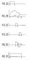
- Fig. 1is a functional block diagram illustrating a defibrillator-pacer 20 comprising a charging circuit 22, a storage capacitor 24, a controller 26, such as for example a micro-controller or a processor (hereinafter controller 26), a user input section 28, output electrodes 32 and 34, an H-bridge 40 and a current control circuit 60.
- the defibrillator-pacer 20is powered by an energy source such as a removable battery (not shown).
- the controller 26controls overall operation of the various components of the defibrillator-pacer 20.
- the H-bridge 40delivers a pulse of electrical energy to a patient via electrodes 32 and 34 under the control of controller 26.
- the defibrillator-pacer 20comprises other well known components which contribute to the overall operation of the defibrillator-pacer 20, such as for example, a patient monitor 27, which acquires and processes the patient's electrocardiogram (ECG) signals, and sends the patient's ECG signals to the controller 26.
- the controller 26controls at least one of timing, amplitude, polarity and shape of energy pulses applied to the patient according to the various modes of operation of the defibrillator-pacer 20.
- Components which are well known and which are not necessary to the understanding of the present inventionare not shown in order to avoid obscuring the embodiments of the invention.
- the H-bridge 40comprises switches 42, 44, 46 and 48 which are driven by switch control circuits 52, 54, 56 and 58, respectively.
- the switch control circuits 52, 54, 56 and 58are controlled in turn by the controller 26.
- the switches 42 and 46have a common connection at a node 43 which is connected to a positive (+) terminal 25 of storage capacitor 24.
- the storage capacitor 24has a negative (-) terminal connected to circuit common 29.
- the switches 44 and 48have a common connection at a node 45 which is also a first node of the current control circuit 60.
- a second node of the current control circuit 60is connected to the circuit common 29.
- the current control circuit 60receives input commands from the controller 26.
- the switches 44 and 46have a common connection at a node 47 which is also connected with the electrode 32 and the switches 42 and 48 have a common connection at a node 49 which is also connected to the electrode 34.
- a resistor RP shown between electrodes 32 and 34represents the effective resistance of the patient.
- Switch contacts 33 and 35are operable to connect the defibrillator-pacer to the patient.
- the switch contacts 33 sand 35are preferably contacts of a relay which operates under control of the controller 26.
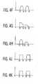
- the controller 26controls the charging circuit 22 in response to an input from the patient monitor 27 or the user input 28, causing the charger to operate for a time interval t 1 - t 2 as shown in Fig. 2A .
- the charging circuit 22charges the storage capacitor 24 during the time interval t 1 - t 2 as shown in Fig 2B to a relative high value, such as for example, 1500 to 2000 volts DC.
- the charging circuit 22discontinues charging the storage capacitor 24 and the voltage of capacitor 24 with respect to circuit common 29 remains at a constant value during a time interval t 2 - t 3.
- the controller 26instructs switch control circuits 52 and 54 to turn on switches 42 and 44, respectively, and instructs the current control circuit 60 to connect node 45 to node 29 either via a fixed low impedance path or to regulate the current passing through the patient.
- switch control circuits 52 and 54instructs switch control circuits 52 and 54 to turn on switches 42 and 44, respectively, and instructs the current control circuit 60 to connect node 45 to node 29 either via a fixed low impedance path or to regulate the current passing through the patient.
- the controller 26again instructs the current control circuit 60 to connect node 45 to node 29 either via the fixed low impedance path or to regulate the current passing through the patient and instructs switch control circuits 56 and 58 to turn on switches 46 and 48, respectively, during a time interval t 5 - t 6 as shown in Fig. 2D .
- the direction of the current applied to the patient via the electrodes 32 and 34is reversed from the direction previously applied during the time interval t 3 - t 4 .
- the current control circuit 60may be commanded to connect node 45 to node 29 at a time t 0 , such as for example, before the beginning of the charging of the capacitor 24 (before the time t 1 ) or before switches 42 and 44 are turned on at the time t 3 .
- the control circuit 60connects nodes 45 and 29 before the voltage across the capacitor 24 exceeds a predetermined value, the stress on components of the current control circuit 60 is significantly reduced, contributing to increased reliability and where a high voltage insulated gate bipolar transistor (IGBT) is used in the H-bridge for commutation, parts with lower voltage ratings may be used in the current control circuit 60, thus again contributing to lower cost.
- IGBTinsulated gate bipolar transistor
- the maximum current applied to the patientis determined by the amplitude of the voltage across the capacitor 24, the effective resistance R P of the patient and the effective impedance of the fixed low impedance path of the current control circuit 60.
- the controller 26controls the charging circuit 22 in response to an input from the patient monitor 27 and the charging circuit 22 charges the storage capacitor 24 during a time interval t 1 - t 2 as shown in Figs. 3A and 2C to a relative low value, such as for example, 75 to 200 volts DC, which may vary dynamically in order to reduce power consumption.
- a relative low valuesuch as for example, 75 to 200 volts DC, which may vary dynamically in order to reduce power consumption.
- the charging circuit 22discontinues charging the storage capacitor 24 and the voltage at node 25 of capacitor 24 with respect to circuit common 29 remains at a constant value during an interval t 2 - t 3 .
- the controller 26instructs switch control circuits 52 and 54 to turn on switches 42 and 44, respectively, and instructs the current control circuit 60 to connect node 45 to node 29 and to regulate the current passing through the patient so as not to exceed a predetermined maximum value.
- Switches 42 and 44are turned on for a time interval t 3 - t 4 as shown in Fig. 3C and current is delivered to the patient R P at electrodes 32 and 34 according to the control of the current control circuit 60 and in a first polarity during the interval t 3 - t 4 as shown in Fig. 3E .
- the controller 26again instructs the current control circuit 60 to connect node 45 to node 29 and to regulate the current passing through the patient and instructs switch control circuits 56 and 58 to turn on switches 46 and 48, respectively, during a time interval t 5 - t 6 as shown in Fig. 3D , reversing the direction of current applied to the patient from the direction previously applied during the time interval t 3 - t 4 .
- the reversed polarity waveformis indicated during the time interval t 5 - t 6 as shown in Fig. 3E .
- Fig. 3EIn Fig.
- the current waveforms applied to the patient for the time intervals t 3 - t 4 and t 5 - t 6are indicated as broken lines, since the shape of the waveform will depend on the character of the current control command, as will be explained more fully below.
- the current control circuit 60comprises a transistor Q1, a resistor R R , an amplifier U1, and a current command circuit 62.
- Resistor R Rhas a first end connected to circuit common 29 and a second end connected to the emitter of transistor Q1.
- the collector of transistor Q1is connected to the H-bridge at the node 45.
- the gate of transistor Q1is connected to the output of amplifier U1 and the non-inverting input (+) of amplifier U1 is connected to the second end of resistor R R so as to form a current follower circuit wherein the current through resistor R R follows the voltage applied at the inverting input (-) of amplifier U1, thus the patient current I P becomes V C divided by R P , where V C is the voltage at the inverting input of amplifier U1.
- the current through the patientis regulated according to the voltage V C applied at the inverting input of amplifier U1.
- the current command interface circuit 62receives commands from the controller 26 and outputs either a fixed value as V C or a time variant value of V C according to a desired mode of operation of the defibrillator-pacer 20.
- the charging circuit 22continuously or periodically replenishes the charge on capacitor 24 to ensure that the voltage at node 25 is sufficiently high to maintain the voltage of the waveform commanded by the time variant V C .
- the value Vcis determined so that transistor Q1 effectively operates as a switch.
- the values of resistor R R and input voltage V Care determined so that Q1 remains in an active region for desired values of patient current.
- the polarity of current applied to the patientis controlled by the H-bridge and the amplitude and waveform of current applied to the patient are controlled by the current regulating circuit 60.
- Figs. 4A-4Ean example of operation of the pacer-defibrillator 20 in a current regulation mode is illustrated.
- the voltage across capacitor 24is assumed to be charged and held at a constant value. It will be readily recognized by persons skilled in the art that if the voltage across capacitor 24 is not maintained at a constant value, that is, allowed to decay as a function of current delivered, the waveform applied to the patient may vary, however, the maximum amplitude of current applied to the patient will still be controlled by the current regulator 60.
- the controller 26causes the switches 42 and 44 to close, determining the polarity of a pulse to be delivered to the patient.
- the controller 26also causes the current command circuit 62 to provide the waveform indicated in Fig. 4D at the time interval t 3 - t 4 to be applied to the inverting input of amplifier U1, thus applying a current to the patient R P during the time interval t 3 - t 4 of the waveform as shown in Fig. 4E .
- a time interval t 5 - t 6as indicated in Fig.
- the controller 26causes the switches 46 and 48 to close, determining the polarity of the pulse to be delivered to the patient to be opposite the polarity of the pulse previously applied during the time interval t 3 - t 4 .
- the controller 26concurrently causes the current command circuit 62 to provide the waveform indicated in Fig. 4D at the time interval t 5 - t 6 to be applied to the inverting input of amplifier U1, thus applying a current of the waveform shown in Fig. 4E at the time interval t 5 - t 6 to the patient who is represented by the resistance R P .
- Q1is operated so as to remain in a linear region, the current waveform I P through the patient R P will follow the voltage waveform V C .
- current waveformssuch as for example, a one-half sine waveform, Fig. 4F , a truncated exponential waveform, Fig. 4G , a damped sine waveform, Fig. 4H , a rectangular waveform, Fig. 4J , and a rounded rectangle waveform, Fig. 4K may be generated.
- the controller 26may be appropriately programmed to cause only one of switch pair 42 and 44 or switch pair 46 and 48 to close and to cause an appropriate voltage waveform to be applied as V C .
- both monophasic and biphasic pulsesare regulated by the present invention.
- Transistor Q1is preferably an insulated gate bipolar transistor (IGBT).
- IGBTfield effect transistor
- a transistor having a lower voltage ratingsuch as for example a field effect transistor (FET) or a junction type bipolar transistor, may be used where it is not desired to regulate the current in the defibrillation mode or where a high voltage IGBT is used in the H-bridge for commutation.
- FETfield effect transistor
- transistor Q1is preferably operated as a switch and fully turned on before the capacitor 24 is charged to high voltages and remain fully turned on until the capacitor has been discharged.
- the sense resistor R R in the current regulating circuit 60 of Fig. 1is selected to optimize regulation of low level pacing pulses. In the fixed low impedance mode, it is advantageous to bypass the resistor R R in the current regulating circuit 60 shown in Fig. 1 .
- a current regulating circuit 60-1which includes a circuit arrangement for bypassing the resistor R R is illustrated.
- the current regulating circuit 60-1operates in a similar manner as the current regulating circuit 60, however the current regulating circuit comprises a transistor Q2 which performs a bypass of the resistor R R and an additional node 65 which receives an input voltage V S1 to operate the bypass.
- the transistor Q2is preferably a power field effect transistor having a source and a drain connected across the resistor R R and a gate connected to the node 65. A voltage rating in the 20 to 50 volt range is adequate for the transistor Q2.
- a current regulating circuit 60-2includes a circuit arrangement for bypassing the resistor R R and a series limiting resistor is illustrated.
- the current regulating circuit 60-2operates in a similar manner as the current regulating circuit 60, however the current regulating circuit 60-2 further comprises a transistor Q2 which performs a bypass of the resistor R R , an additional node 65 which receives an input voltage V S1 to operate the bypass of R R , a series limiting resistor R L , a transistor Q3 which bypasses the resistor R L and a node 67 which receives a voltage V S2 which operates the bypass of R L .
- the transistor Q2is preferably a power field effect transistor having a source and a drain connected across the resistor R R and a gate connected to the node 65. A voltage rating of transistor Q2 in the 20 to 50 volt range is adequate.
- the series limiting resistor R Lis inserted between the collector of Q1 and the node 45. The series resistor R L is used where it is desirable to have additional limiting, such as for example, in the pacer mode.
- the transistor Q3performs a bypass of the resistor R L in response to an input voltage V S2 received at node 67.
- the transistor Q3is preferably a power field effect transistor having a source and a drain connected across the resistor R L and a gate connected to the node 67.
- a voltage rating of transistor Q3should be in the 50 to 200 volt range or higher. Where it is desirable to bypass both the resistors R L and R R simultaneously, the voltage VS1 should be applied before the voltage VS2 so that a ground reference is established for the transistor Q3. Otherwise, a more complex gate drive for the transistor Q3 is required.
- switches 44 and 48( Fig. 1 ) are high voltage switching components. Where the switches 44 and 48 of the H-bridge are high voltage switching components, Q1 may be a MOSFET having a voltage range of 200 volts or greater.
- Defibrillator-pacersmay also incorporate additional circuitry (not shown) which avoids application of the capacitor voltage to the H-bridge components during standby operations or which disconnects the patient from the outputs of the H-bridge during standby operations, such as for example, a relay may be incorporated between the patient and the H-bridge.
Landscapes
- Health & Medical Sciences (AREA)
- Cardiology (AREA)
- Heart & Thoracic Surgery (AREA)
- Engineering & Computer Science (AREA)
- Biomedical Technology (AREA)
- Nuclear Medicine, Radiotherapy & Molecular Imaging (AREA)
- Radiology & Medical Imaging (AREA)
- Life Sciences & Earth Sciences (AREA)
- Animal Behavior & Ethology (AREA)
- General Health & Medical Sciences (AREA)
- Public Health (AREA)
- Veterinary Medicine (AREA)
- Electrotherapy Devices (AREA)
Description
- This invention relates to an apparatus for delivering electrical energy to a patient for maintaining and/or restoring the pumping rhythm of a heart, and more particularly to an apparatus for regulating a current flow to the patent to conform with a predetermined maximum value and/or according to a predetermined waveform. A single power source is provided to deliver current with either pacing or defibrillation energy.
- The frequent occurrence of sudden cardiac arrest (SCA) is well known. SCA occurs when the heart stops pumping blood, usually due to abnormal electrical activity in the heart, such as for example, ventricular fibrillation, which is caused very fast electrical activity in the heart. Ventricular fibrillation is treated by applying an electric shock to the patient's heart through the use of a defibrillator. Other forms of abnormal cardiac rhythms, such as bradycardia (slow heart rate) and tachycardia (rapid heart rate) may be treated with a low voltage pacing pulse, which assists the heart's natural pacemakers. Devices which accomplish both defibrillation and pacing typically include two power sources, two capacitors, and two control mechanisms, one for the high energy defibrillation pulse and one for the lower energy pacing pulses. This double circuitry ultimately increases the weight size, and cost of the device.
US 6 208 895 B1 discloses an external defibrillator/pacer which includes an H-bridge coupled to an energy storage capacitor. The energy storage capacitor delivers an external defibrillation pulse with stored energy during a defibrillation mode and an external pacing pulse during a pacing mode. A similar defibrillator/pacer is disclosed inWO 01/26731 - There is a need for an apparatus which performs both defibrillation and pacing and which uses a single power source, a single high energy capacitor and a single control mechanism to deliver either defibrillation or pacing energy.
- The present invention is a defibrillator-pacer for delivering electrical energy to a patient as either defibrillation pulses or pacing pulses. The defibrillator-pacer comprises a power source, an H-bridge comprising a plurality of switches which control the delivery of the electrical energy from the power source to the patient; and a current control circuit which regulates electrical current supplied to the patient, wherein the current control circuit is serially connected with the H-bridge. The current control circuit regulates the current in response to a current control signal as determined by a controller. The current control signal may be a constant value or a time varying signal having a predetermined or varying waveform. The current control circuit may be operable such that the current control signal has a first value where a first pair of switches of the H-bridge is operated and a second value where a second pair of the switches of the H-bridge is operated. The circuit may be also operable wherein the current control signal has a waveform of a first shape where a first pair of the switches of the H-bridge is operated and a waveform of a second shape where a second pair of the switches of the H-bridge is operated. Various shapes of the control signal waveform may include sinusoidal, rectangular and truncated exponential waveforms. The current control circuit is also operable as a switch which may be operated prior to the operation of either pair of H-bridge switches. The H-bridge switches are operable in conjunction with the current control circuit to deliver a controlled current biphasic pulse to the patient.
- A defibrillator-pacer incorporating the inventive circuit comprises a storage circuit having first and second terminals, the storage circuit operable to store electrical energy; an H-bridge circuit, coupled to the first terminal of the storage circuit, adapted to couple with the patient and operable to deliver electrical current from the stored electrical energy to the patient; and a current control circuit, coupled with the H-bridge circuit and operable to electrically connect the H-bridge circuit with the second terminal of the storage circuit, to regulate the delivery of the electrical current to the patient. The current control circuit, which is operable in a linear mode and responsive to a control voltage, may comprise an amplifier, a transistor and a resistor arranged as a voltage to current follower. A controller controls the H-bridge to control the polarity of the electrical current delivered to the patient and determines the control voltage optionally as a fixed value or a time varying waveform, which may be, for example, a sinusoidal waveform, a half-sinusoidal waveform, a rectangular waveform or a decaying exponential waveform.
- In a first alternate embodiment of the current control circuit, a first transistor, an amplifier and a resistor are arranged as a voltage to current follower to control the current through the patient according to a predetermined scale factor determined by the resistor and a first control voltage, and a second transistor is arranged to selectively bypass the first resistor in response to a second control voltage to change the scale factor of the voltage to current follower.
- In a second alternate embodiment of the control circuit, a first resistor is connected in series with the H-bridge to passively limit the current through the patient. A first transistor, an amplifier and a second resistor are arranged as a voltage to current follower to control the current through the patient according to a predetermined scale factor determined by the first resistor, the second resistor and a first control voltage. A second transistor bypasses the first resistor in response to a second control voltage to change the scale factor of the voltage to current follower and a third transistor bypasses the second resistor in response to a third control voltage to further change the scale factor of the voltage to current follower.
- The present invention will become more apparent and more readily appreciated from the following description of the various embodiments, taken in conjunction with the accompanying drawings in which:
Fig. 1 is a functional block diagram illustrating a defibrillator-pacer circuit according to an embodiment of the present invention.Figs. 2A - 2F are waveforms illustrating delivery of a current where the circuit shown inFig. 1 is operated in an unregulated mode.Figs. 3A - 3F are waveforms illustrating delivery of a current where the circuit shown inFig. 1 is operated in a current regulated mode.Figs. 4A - 4K are waveforms illustrating delivery of a current where the circuit shown inFig. 1 is operated in a current regulated mode from a power source having a constant value.Fig. 5 is an schematic diagram of an alternate construction of a current regulating portion of the defibrillator-pacer circuit shown inFig. 1 .Fig. 6 is an schematic diagram of another alternate construction of a current regulating portion of the defibrillator-pacer circuit shown inFig. 1 .- Reference will now be made in detail to the present embodiments of the present invention, examples of which are illustrated in the accompanying drawings, wherein like reference numerals refer to like elements throughout.
- The present invention is operable in a first mode which provides either a high energy monophasic or a biphasic electrical pulse to a patient via electrodes applied to the chest of a patient and operable in a second mode which provides lower energy pacing pulses to the patient. Monophasic defibrillators deliver an electrical current pulse of a single polarity. Biphasic defibrillators deliver an electrical current pulse of a first polarity followed by an electrical current pulse of the opposite polarity. Where delivered external to the patient, these electrical pulses are high energy (typically in the range of 30 J to 360 J). The present invention may be employed by defibrillators or pacers intended to generate monophasic, biphasic or multiphasic waveforms and may be employed by defibrillators that allow the user to select the waveform type. Finally, the present invention may be employed in either external or implantable defibrillators or pacers. It is believed that the invention described herein is primarily beneficial for defibrillators that combine defibrillation with pacing.
Fig. 1 is a functional block diagram illustrating a defibrillator-pacer 20 comprising acharging circuit 22, astorage capacitor 24, acontroller 26, such as for example a micro-controller or a processor (hereinafter controller 26), auser input section 28,output electrodes bridge 40 and acurrent control circuit 60. The defibrillator-pacer 20 is powered by an energy source such as a removable battery (not shown). Thecontroller 26 controls overall operation of the various components of the defibrillator-pacer 20. The H-bridge 40 delivers a pulse of electrical energy to a patient viaelectrodes controller 26. The defibrillator-pacer 20 comprises other well known components which contribute to the overall operation of the defibrillator-pacer 20, such as for example, apatient monitor 27, which acquires and processes the patient's electrocardiogram (ECG) signals, and sends the patient's ECG signals to thecontroller 26. Thecontroller 26 controls at least one of timing, amplitude, polarity and shape of energy pulses applied to the patient according to the various modes of operation of the defibrillator-pacer 20. Components which are well known and which are not necessary to the understanding of the present invention are not shown in order to avoid obscuring the embodiments of the invention.- The H-
bridge 40 comprisesswitches switch control circuits switch control circuits controller 26. Theswitches node 43 which is connected to a positive (+)terminal 25 ofstorage capacitor 24. Thestorage capacitor 24 has a negative (-) terminal connected to circuit common 29. Theswitches 44 and 48 have a common connection at anode 45 which is also a first node of thecurrent control circuit 60. A second node of thecurrent control circuit 60 is connected to the circuit common 29. Thecurrent control circuit 60 receives input commands from thecontroller 26. Theswitches 44 and 46 have a common connection at a node 47 which is also connected with theelectrode 32 and theswitches node 49 which is also connected to theelectrode 34. A resistor RP shown betweenelectrodes contacts switch contacts 33sand 35 are preferably contacts of a relay which operates under control of thecontroller 26. - Referring now to
Figs. 2A-2F , one mode of operation of the circuit shown inFig. 1 will be described. Thecontroller 26 controls the chargingcircuit 22 in response to an input from the patient monitor 27 or theuser input 28, causing the charger to operate for a time interval t1- t2 as shown inFig. 2A . The chargingcircuit 22 charges thestorage capacitor 24 during the time interval t1 - t2 as shown inFig 2B to a relative high value, such as for example, 1500 to 2000 volts DC. At the time t2, the chargingcircuit 22 discontinues charging thestorage capacitor 24 and the voltage ofcapacitor 24 with respect to circuit common 29 remains at a constant value during a time interval t2 - t3. - Where the defibrillator-
pacer 20 is operated as a defibrillator in a biphasic mode, thecontroller 26 instructsswitch control circuits current control circuit 60 to connectnode 45 tonode 29 either via a fixed low impedance path or to regulate the current passing through the patient. Although current regulation presently has little known value at high energy defibrillation discharges, and may be impractical dissipation wise with current known technology, current regulation of low energies of up to 2 joules is believed to be both practical and beneficial.Switches 42 and 44 are turned on for the time interval t3 - t4 as shown inFig. 2C and where thecurrent control circuit 60 is operating as a fixed low impedance path, current is delivered to the patient RP via theelectrodes Fig. 2E . - During a time interval t4 - t5, the voltage across the storage capacitor remains at a relatively constant reduced value. At the time t5, the
controller 26 again instructs thecurrent control circuit 60 to connectnode 45 tonode 29 either via the fixed low impedance path or to regulate the current passing through the patient and instructsswitch control circuits Fig. 2D . During the time interval t5 - t6, the direction of the current applied to the patient via theelectrodes current control circuit 60 connectsnode 45 tonode 29 via the fixed low impedance path, current is applied to the patient RP atelectrodes Fig. 2E . - Alternately, the
current control circuit 60 may be commanded to connectnode 45 tonode 29 at a time t0, such as for example, before the beginning of the charging of the capacitor 24 (before the time t1) or beforeswitches 42 and 44 are turned on at the time t3. Where thecontrol circuit 60 connectsnodes capacitor 24 exceeds a predetermined value, the stress on components of thecurrent control circuit 60 is significantly reduced, contributing to increased reliability and where a high voltage insulated gate bipolar transistor (IGBT) is used in the H-bridge for commutation, parts with lower voltage ratings may be used in thecurrent control circuit 60, thus again contributing to lower cost. - Where the
current regulating circuit 60 is operated in the fixed low impedance mode, the maximum current applied to the patient is determined by the amplitude of the voltage across thecapacitor 24, the effective resistance RP of the patient and the effective impedance of the fixed low impedance path of thecurrent control circuit 60. - Referring now to
Figs. 3A-3D , the operation of the circuit shown inFig. 1 will be further described relative to operation in a pacing mode. Thecontroller 26 controls the chargingcircuit 22 in response to an input from the patient monitor 27 and the chargingcircuit 22 charges thestorage capacitor 24 during a time interval t1 - t2 as shown inFigs. 3A and2C to a relative low value, such as for example, 75 to 200 volts DC, which may vary dynamically in order to reduce power consumption. At the time t2, the chargingcircuit 22 discontinues charging thestorage capacitor 24 and the voltage atnode 25 ofcapacitor 24 with respect to circuit common 29 remains at a constant value during an interval t2 - t3. - Where the defibrillator-pacer is operated as a pacer in a biphasic mode, the
controller 26 instructsswitch control circuits current control circuit 60 to connectnode 45 tonode 29 and to regulate the current passing through the patient so as not to exceed a predetermined maximum value.Switches 42 and 44 are turned on for a time interval t3 - t4 as shown inFig. 3C and current is delivered to the patient RP atelectrodes current control circuit 60 and in a first polarity during the interval t3 - t4 as shown inFig. 3E . At a time t5, thecontroller 26 again instructs thecurrent control circuit 60 to connectnode 45 tonode 29 and to regulate the current passing through the patient and instructsswitch control circuits Fig. 3D , reversing the direction of current applied to the patient from the direction previously applied during the time interval t3 - t4. The reversed polarity waveform is indicated during the time interval t5 - t6 as shown inFig. 3E . InFig. 3E , the current waveforms applied to the patient for the time intervals t3 - t4 and t5 - t6 are indicated as broken lines, since the shape of the waveform will depend on the character of the current control command, as will be explained more fully below. - Referring again to
Fig. 1 , thecurrent control circuit 60 comprises a transistor Q1, a resistor RR, an amplifier U1, and acurrent command circuit 62. Resistor RR has a first end connected to circuit common 29 and a second end connected to the emitter of transistor Q1. The collector of transistor Q1 is connected to the H-bridge at thenode 45. The gate of transistor Q1 is connected to the output of amplifier U1 and the non-inverting input (+) of amplifier U1 is connected to the second end of resistor RR so as to form a current follower circuit wherein the current through resistor RR follows the voltage applied at the inverting input (-) of amplifier U1, thus the patient current IP becomes VC divided by RP, where VC is the voltage at the inverting input of amplifier U1. Thus, the current through the patient is regulated according to the voltage VC applied at the inverting input of amplifier U1. The currentcommand interface circuit 62 receives commands from thecontroller 26 and outputs either a fixed value as VC or a time variant value of VC according to a desired mode of operation of the defibrillator-pacer 20. During operation of the defibrillator-pacer where patient current is being controlled by thecurrent control circuit 60, the chargingcircuit 22 continuously or periodically replenishes the charge oncapacitor 24 to ensure that the voltage atnode 25 is sufficiently high to maintain the voltage of the waveform commanded by the time variant VC. Where it is desired to operate the defibrillator-pacer 20 whereinnode 45 is connected tonode 29 via the fixed low impedance path, the value Vc is determined so that transistor Q1 effectively operates as a switch. Where it is desired to operate the defibrillator-pacer 20 so that thecurrent regulating circuit 60 controls the current passing betweennodes current regulating circuit 60. - Referring to
Figs. 4A-4E , an example of operation of the pacer-defibrillator 20 in a current regulation mode is illustrated. For simplicity of explanation, the voltage acrosscapacitor 24 is assumed to be charged and held at a constant value. It will be readily recognized by persons skilled in the art that if the voltage acrosscapacitor 24 is not maintained at a constant value, that is, allowed to decay as a function of current delivered, the waveform applied to the patient may vary, however, the maximum amplitude of current applied to the patient will still be controlled by thecurrent regulator 60. - As shown in
Fig. 4A , the voltage acrosscapacitor 24 is charged to a constant value at a time t1. At a time interval t3 - t4 indicated inFig. 4B , thecontroller 26 causes theswitches 42 and 44 to close, determining the polarity of a pulse to be delivered to the patient. Thecontroller 26 also causes thecurrent command circuit 62 to provide the waveform indicated inFig. 4D at the time interval t3 - t4 to be applied to the inverting input of amplifier U1, thus applying a current to the patient RP during the time interval t3 - t4 of the waveform as shown inFig. 4E . Next, at a time interval t5 - t6 as indicated inFig. 4C , thecontroller 26 causes theswitches controller 26 concurrently causes thecurrent command circuit 62 to provide the waveform indicated inFig. 4D at the time interval t5 - t6 to be applied to the inverting input of amplifier U1, thus applying a current of the waveform shown inFig. 4E at the time interval t5 - t6 to the patient who is represented by the resistance RP. Where Q1 is operated so as to remain in a linear region, the current waveform IP through the patient RP will follow the voltage waveform VC. Thus, current waveforms, such as for example, a one-half sine waveform,Fig. 4F , a truncated exponential waveform,Fig. 4G , a damped sine waveform,Fig. 4H , a rectangular waveform,Fig. 4J , and a rounded rectangle waveform,Fig. 4K may be generated. A person skilled in the art will recognize that where a controlled current mono-phasic waveform is desired, thecontroller 26 may be appropriately programmed to cause only one ofswitch pair 42 and 44 orswitch pair - Transistor Q1 is preferably an insulated gate bipolar transistor (IGBT). A transistor having a lower voltage rating, such as for example a field effect transistor (FET) or a junction type bipolar transistor, may be used where it is not desired to regulate the current in the defibrillation mode or where a high voltage IGBT is used in the H-bridge for commutation. Where a transistor having a lower voltage rating is used, transistor Q1 is preferably operated as a switch and fully turned on before the
capacitor 24 is charged to high voltages and remain fully turned on until the capacitor has been discharged. - Preferably, the sense resistor RR in the
current regulating circuit 60 ofFig. 1 is selected to optimize regulation of low level pacing pulses. In the fixed low impedance mode, it is advantageous to bypass the resistor RR in thecurrent regulating circuit 60 shown inFig. 1 . Referring now toFig. 5 , a current regulating circuit 60-1 which includes a circuit arrangement for bypassing the resistor RR is illustrated. The current regulating circuit 60-1 operates in a similar manner as thecurrent regulating circuit 60, however the current regulating circuit comprises a transistor Q2 which performs a bypass of the resistor RR and anadditional node 65 which receives an input voltage VS1 to operate the bypass. The transistor Q2 is preferably a power field effect transistor having a source and a drain connected across the resistor RR and a gate connected to thenode 65. A voltage rating in the 20 to 50 volt range is adequate for the transistor Q2. - Referring now to
Fig. 6 , a current regulating circuit 60-2 includes a circuit arrangement for bypassing the resistor RR and a series limiting resistor is illustrated. The current regulating circuit 60-2 operates in a similar manner as thecurrent regulating circuit 60, however the current regulating circuit 60-2 further comprises a transistor Q2 which performs a bypass of the resistor RR, anadditional node 65 which receives an input voltage VS1 to operate the bypass of RR, a series limiting resistor RL, a transistor Q3 which bypasses the resistor RL and anode 67 which receives a voltage VS2 which operates the bypass of RL. The transistor Q2 is preferably a power field effect transistor having a source and a drain connected across the resistor RR and a gate connected to thenode 65. A voltage rating of transistor Q2 in the 20 to 50 volt range is adequate. The series limiting resistor RL is inserted between the collector of Q1 and thenode 45. The series resistor RL is used where it is desirable to have additional limiting, such as for example, in the pacer mode. The transistor Q3 performs a bypass of the resistor RL in response to an input voltage VS2 received atnode 67. The transistor Q3 is preferably a power field effect transistor having a source and a drain connected across the resistor RL and a gate connected to thenode 67. A voltage rating of transistor Q3 should be in the 50 to 200 volt range or higher. Where it is desirable to bypass both the resistors RL and RR simultaneously, the voltage VS1 should be applied before the voltage VS2 so that a ground reference is established for the transistor Q3. Otherwise, a more complex gate drive for the transistor Q3 is required. Where the circuit configuration ofFig. 6 is employed, switches 44 and 48 (Fig. 1 ) are high voltage switching components. Where theswitches 44 and 48 of the H-bridge are high voltage switching components, Q1 may be a MOSFET having a voltage range of 200 volts or greater. - Defibrillator-pacers according to the present invention may also incorporate additional circuitry (not shown) which avoids application of the capacitor voltage to the H-bridge components during standby operations or which disconnects the patient from the outputs of the H-bridge during standby operations, such as for example, a relay may be incorporated between the patient and the H-bridge.
- Although a few embodiments of the present invention have been shown and described, it will be appreciated by those skilled in the art that changes may be made in these embodiments without departing from the scope of the invention, which is defined in the claims.
Claims (7)
- A defibrillator-pacer for delivering electrical energy to a patient, the defibrillator-pacer comprising:a storage circuit (24) having first and second terminals (25, 29), the storage circuit operable to store electrical energy;an H-bridge circuit (40), coupled to the first terminal (25) of the storage circuit, adapted to couple with the patient (RP) and operable to deliver electrical current from the storage circuit energy to the patient;a current control circuit (60), coupled with the H-bridge circuit and operable to electrically connect the H-bridge circuit with the second terminal (29) of the storage circuit, to regulate the delivery of the electrical energy to the patient by the H-bridge circuit, wherein the current control circuit is configured to operate in a linear mode and responsive to a control voltage; anda controller (26) which is operable
to control the H-bridge (40) to control the polarity of the electrical current delivered to the patient; and
to determine the control voltage. - The defibrillator-pacer according to claim 1, wherein the current control circuit comprises an amplifier (U1), a transistor (Q1) and a resistor (RR) arranged as a voltage to current follower.
- The defibrillator-pacer according to claim 1, wherein the control voltage is a fixed value.
- The defibrillator-pacer according to claim 1, wherein the control voltage has a time varying waveform (Figs. 4B-4K).
- A defibrillator-pacer according to claim 1, the control circuit comprising:a first transistor (Q1), an amplifier (U1) and a resistor (RR) arranged as a voltage to current follower which controls the current through the patient according to a predetermined scale factor determined by the resistor and a first control voltage, anda second transistor (Q2) which bypasses the first resistor (RR) in response to a second control voltage (VS1) to change the scale factor of the voltage to current follower.
- A defibrillator-pacer according to claim 1, the control circuit comprising:a first resistor (RL) connected in series with the H-bridge which limits the current through the patient;a first transistor (Q1), an amplifier (U1) and a second resistor (RP) arranged as a voltage to current follower which controls the current through the patient according to a predetermined scale factor determined by the first resistor, the second resistor and a first control voltage,a second transistor (Q3) which bypasses the first resistor in response to a second control voltage (VS2) to change the scale factor of the voltage to current follower.
- The defibrillator-pacer according to claim 6, wherein the control circuit further comprises:a third transistor (Q2) which bypasses the second resistor (RR) in response to a third control voltage (VS1) to further change the scale factor of the voltage to current follower.
Applications Claiming Priority (3)
| Application Number | Priority Date | Filing Date | Title |
|---|---|---|---|
| US24763 | 2001-12-20 | ||
| US10/024,763US6952607B2 (en) | 2001-12-20 | 2001-12-20 | Method and apparatus for delivering defibrillation and pacing energy from a single power source |
| PCT/IB2002/005099WO2003053518A1 (en) | 2001-12-20 | 2002-12-02 | Method and apparatus for delivering defibrillation and pacing energy from a single power source |
Publications (2)
| Publication Number | Publication Date |
|---|---|
| EP1458445A1 EP1458445A1 (en) | 2004-09-22 |
| EP1458445B1true EP1458445B1 (en) | 2015-11-04 |
Family
ID=21822279
Family Applications (1)
| Application Number | Title | Priority Date | Filing Date |
|---|---|---|---|
| EP02785807.5AExpired - LifetimeEP1458445B1 (en) | 2001-12-20 | 2002-12-02 | Apparatus for delivering defibrillation and pacing energy from a single power source |
Country Status (5)
| Country | Link |
|---|---|
| US (1) | US6952607B2 (en) |
| EP (1) | EP1458445B1 (en) |
| JP (1) | JP4532904B2 (en) |
| AU (1) | AU2002351094A1 (en) |
| WO (1) | WO2003053518A1 (en) |
Cited By (2)
| Publication number | Priority date | Publication date | Assignee | Title |
|---|---|---|---|---|
| RU181259U1 (en)* | 2018-03-06 | 2018-07-06 | Общество с ограниченной ответственностью Концерн "Аксион" (ООО Концерн "Аксион") | DEVICE FOR FORMING A BIPOLAR PULSE |
| US10946207B2 (en) | 2017-05-27 | 2021-03-16 | West Affum Holdings Corp. | Defibrillation waveforms for a wearable cardiac defibrillator |
Families Citing this family (8)
| Publication number | Priority date | Publication date | Assignee | Title |
|---|---|---|---|---|
| US6885562B2 (en)* | 2001-12-28 | 2005-04-26 | Medtronic Physio-Control Manufacturing Corporation | Circuit package and method for making the same |
| US8712510B2 (en)* | 2004-02-06 | 2014-04-29 | Q-Tec Systems Llc | Method and apparatus for exercise monitoring combining exercise monitoring and visual data with wireless internet connectivity |
| US7555338B2 (en) | 2005-04-26 | 2009-06-30 | Cameron Health, Inc. | Methods and implantable devices for inducing fibrillation by alternating constant current |
| US7877139B2 (en)* | 2006-09-22 | 2011-01-25 | Cameron Health, Inc. | Method and device for implantable cardiac stimulus device lead impedance measurement |
| US9987493B2 (en)* | 2008-10-28 | 2018-06-05 | Medtronic, Inc. | Medical devices and methods for delivery of current-based electrical stimulation therapy |
| US9056206B2 (en)* | 2008-10-28 | 2015-06-16 | Medtronic, Inc. | Adaptable current regulator for delivery of current-based electrical stimulation therapy |
| US9259571B2 (en)* | 2009-10-21 | 2016-02-16 | Medtronic, Inc. | Electrical stimulation therapy using decaying current pulses |
| US11305128B1 (en) | 2019-07-09 | 2022-04-19 | Avive Solutions, Inc. | Defibrillator discharge testing |
Family Cites Families (7)
| Publication number | Priority date | Publication date | Assignee | Title |
|---|---|---|---|---|
| US5906633A (en)* | 1996-10-29 | 1999-05-25 | Pacesetter, Inc. | System for delivering rounded low pain therapeutic electrical waveforms to the heart |
| US6175765B1 (en)* | 1997-03-05 | 2001-01-16 | Medtronic Physio-Control Manufacturing Corp. | H-bridge circuit for generating a high-energy biphasic waveform in an external defibrillator |
| US6035235A (en)* | 1998-03-30 | 2000-03-07 | Angeion Corp. | Amplified voltage output switching network for a self-powered defibrillator |
| US6208895B1 (en)* | 1998-10-13 | 2001-03-27 | Physio-Control Manufacturing Corporation | Circuit for performing external pacing and biphasic defibrillation |
| US6104953A (en)* | 1999-01-28 | 2000-08-15 | Heartstream, Inc. | Method and apparatus for delivering defibrillation and pacing energy from a single power source |
| US6094597A (en)* | 1999-02-05 | 2000-07-25 | Medtronic, Inc. | Implantable medical device incorporating distributed core, step-up transformer |
| FI19992219A7 (en) | 1999-10-14 | 2001-04-15 | Instr Oyj | Combined defibrillator and pacemaker |
- 2001
- 2001-12-20USUS10/024,763patent/US6952607B2/ennot_activeExpired - Lifetime
- 2002
- 2002-12-02WOPCT/IB2002/005099patent/WO2003053518A1/enactiveApplication Filing
- 2002-12-02AUAU2002351094Apatent/AU2002351094A1/ennot_activeAbandoned
- 2002-12-02EPEP02785807.5Apatent/EP1458445B1/ennot_activeExpired - Lifetime
- 2002-12-02JPJP2003554274Apatent/JP4532904B2/ennot_activeExpired - Fee Related
Cited By (3)
| Publication number | Priority date | Publication date | Assignee | Title |
|---|---|---|---|---|
| US10946207B2 (en) | 2017-05-27 | 2021-03-16 | West Affum Holdings Corp. | Defibrillation waveforms for a wearable cardiac defibrillator |
| US11648411B2 (en) | 2017-05-27 | 2023-05-16 | West Affum Holdings Dac | Defibrillation waveforms for a wearable cardiac defibrillator |
| RU181259U1 (en)* | 2018-03-06 | 2018-07-06 | Общество с ограниченной ответственностью Концерн "Аксион" (ООО Концерн "Аксион") | DEVICE FOR FORMING A BIPOLAR PULSE |
Also Published As
| Publication number | Publication date |
|---|---|
| AU2002351094A1 (en) | 2003-07-09 |
| US6952607B2 (en) | 2005-10-04 |
| WO2003053518A1 (en) | 2003-07-03 |
| JP2005512697A (en) | 2005-05-12 |
| EP1458445A1 (en) | 2004-09-22 |
| US20030120310A1 (en) | 2003-06-26 |
| JP4532904B2 (en) | 2010-08-25 |
Similar Documents
| Publication | Publication Date | Title |
|---|---|---|
| US6047212A (en) | External defibrillator capable of delivering patient impedance compensated biphasic waveforms | |
| US9522284B2 (en) | Defibrillation pacing circuitry | |
| EP0808639B1 (en) | Patient-worn energy delivery apparatus | |
| US5733310A (en) | Electrotherapy circuit and method for producing therapeutic discharge waveform immediately following sensing pulse | |
| US5769872A (en) | Electrotherapy circuit and method for shaping current waveforms | |
| US6096063A (en) | Electrotherapy circuit having controlled current discharge based on patient-dependent electrical parameter | |
| US20010027330A1 (en) | Circuit for performing external pacing and biphasic defibrillation | |
| US6104953A (en) | Method and apparatus for delivering defibrillation and pacing energy from a single power source | |
| US6968230B2 (en) | H-bridge circuit for generating a high-energy biphasic and external pacing waveform in an external defibrillator | |
| EP0973582B1 (en) | Electrotherapy current waveform | |
| EP1458445B1 (en) | Apparatus for delivering defibrillation and pacing energy from a single power source | |
| US5797968A (en) | Electrotherapy circuit for producing current waveform with sawtooth ripple | |
| EP0956095B1 (en) | Hochenergiedefibrillator mit stromkontrollschaltung | |
| US7860565B2 (en) | Defibrillator having a switched mode power supply for transcutaneous pacing | |
| US5904706A (en) | Method and apparatus for producing electrotherapy current waveform with ripple | |
| US5800463A (en) | Electrotherapy circuit having controlled peak current | |
| US5800462A (en) | Electrotherapy circuit for producing therapeutic discharge waveform based on high-current sensing pulse | |
| US20060122657A1 (en) | Programmable voltage-waveform-generating battery power source for implantable medical use | |
| WO1997031680A1 (en) | Electrotherapy method and apparatus | |
| WO2006060411A2 (en) | Programmable voltage-waveform-generating battery power source for implantable medical use |
Legal Events
| Date | Code | Title | Description |
|---|---|---|---|
| PUAI | Public reference made under article 153(3) epc to a published international application that has entered the european phase | Free format text:ORIGINAL CODE: 0009012 | |
| 17P | Request for examination filed | Effective date:20040720 | |
| AK | Designated contracting states | Kind code of ref document:A1 Designated state(s):AT BE BG CH CY CZ DE DK EE ES FI FR GB GR IE IT LI LU MC NL PT SE SK TR | |
| AX | Request for extension of the european patent | Extension state:AL LT LV MK RO | |
| 17Q | First examination report despatched | Effective date:20100506 | |
| RAP1 | Party data changed (applicant data changed or rights of an application transferred) | Owner name:KONINKLIJKE PHILIPS N.V. | |
| GRAP | Despatch of communication of intention to grant a patent | Free format text:ORIGINAL CODE: EPIDOSNIGR1 | |
| INTG | Intention to grant announced | Effective date:20150529 | |
| GRAS | Grant fee paid | Free format text:ORIGINAL CODE: EPIDOSNIGR3 | |
| GRAA | (expected) grant | Free format text:ORIGINAL CODE: 0009210 | |
| AK | Designated contracting states | Kind code of ref document:B1 Designated state(s):AT BE BG CH CY CZ DE DK EE ES FI FR GB GR IE IT LI LU MC NL PT SE SK TR | |
| REG | Reference to a national code | Ref country code:GB Ref legal event code:FG4D | |
| REG | Reference to a national code | Ref country code:CH Ref legal event code:EP | |
| REG | Reference to a national code | Ref country code:AT Ref legal event code:REF Ref document number:758774 Country of ref document:AT Kind code of ref document:T Effective date:20151115 | |
| REG | Reference to a national code | Ref country code:IE Ref legal event code:FG4D | |
| REG | Reference to a national code | Ref country code:DE Ref legal event code:R082 Ref document number:60247600 Country of ref document:DE Representative=s name:MEISSNER, BOLTE & PARTNER GBR, DE Ref country code:DE Ref legal event code:R082 Ref document number:60247600 Country of ref document:DE Representative=s name:MEISSNER BOLTE PATENTANWAELTE RECHTSANWAELTE P, DE | |
| REG | Reference to a national code | Ref country code:DE Ref legal event code:R096 Ref document number:60247600 Country of ref document:DE | |
| REG | Reference to a national code | Ref country code:FR Ref legal event code:PLFP Year of fee payment:14 | |
| REG | Reference to a national code | Ref country code:NL Ref legal event code:MP Effective date:20151104 | |
| REG | Reference to a national code | Ref country code:AT Ref legal event code:MK05 Ref document number:758774 Country of ref document:AT Kind code of ref document:T Effective date:20151104 | |
| PG25 | Lapsed in a contracting state [announced via postgrant information from national office to epo] | Ref country code:ES Free format text:LAPSE BECAUSE OF FAILURE TO SUBMIT A TRANSLATION OF THE DESCRIPTION OR TO PAY THE FEE WITHIN THE PRESCRIBED TIME-LIMIT Effective date:20151104 Ref country code:IT Free format text:LAPSE BECAUSE OF FAILURE TO SUBMIT A TRANSLATION OF THE DESCRIPTION OR TO PAY THE FEE WITHIN THE PRESCRIBED TIME-LIMIT Effective date:20151104 Ref country code:NL Free format text:LAPSE BECAUSE OF FAILURE TO SUBMIT A TRANSLATION OF THE DESCRIPTION OR TO PAY THE FEE WITHIN THE PRESCRIBED TIME-LIMIT Effective date:20151104 | |
| PG25 | Lapsed in a contracting state [announced via postgrant information from national office to epo] | Ref country code:FI Free format text:LAPSE BECAUSE OF FAILURE TO SUBMIT A TRANSLATION OF THE DESCRIPTION OR TO PAY THE FEE WITHIN THE PRESCRIBED TIME-LIMIT Effective date:20151104 Ref country code:SE Free format text:LAPSE BECAUSE OF FAILURE TO SUBMIT A TRANSLATION OF THE DESCRIPTION OR TO PAY THE FEE WITHIN THE PRESCRIBED TIME-LIMIT Effective date:20151104 Ref country code:GR Free format text:LAPSE BECAUSE OF FAILURE TO SUBMIT A TRANSLATION OF THE DESCRIPTION OR TO PAY THE FEE WITHIN THE PRESCRIBED TIME-LIMIT Effective date:20160205 Ref country code:BE Free format text:LAPSE BECAUSE OF NON-PAYMENT OF DUE FEES Effective date:20151231 Ref country code:AT Free format text:LAPSE BECAUSE OF FAILURE TO SUBMIT A TRANSLATION OF THE DESCRIPTION OR TO PAY THE FEE WITHIN THE PRESCRIBED TIME-LIMIT Effective date:20151104 Ref country code:PT Free format text:LAPSE BECAUSE OF FAILURE TO SUBMIT A TRANSLATION OF THE DESCRIPTION OR TO PAY THE FEE WITHIN THE PRESCRIBED TIME-LIMIT Effective date:20160304 | |
| PG25 | Lapsed in a contracting state [announced via postgrant information from national office to epo] | Ref country code:CZ Free format text:LAPSE BECAUSE OF FAILURE TO SUBMIT A TRANSLATION OF THE DESCRIPTION OR TO PAY THE FEE WITHIN THE PRESCRIBED TIME-LIMIT Effective date:20151104 | |
| REG | Reference to a national code | Ref country code:CH Ref legal event code:PL | |
| REG | Reference to a national code | Ref country code:DE Ref legal event code:R097 Ref document number:60247600 Country of ref document:DE | |
| PG25 | Lapsed in a contracting state [announced via postgrant information from national office to epo] | Ref country code:SK Free format text:LAPSE BECAUSE OF FAILURE TO SUBMIT A TRANSLATION OF THE DESCRIPTION OR TO PAY THE FEE WITHIN THE PRESCRIBED TIME-LIMIT Effective date:20151104 Ref country code:EE Free format text:LAPSE BECAUSE OF FAILURE TO SUBMIT A TRANSLATION OF THE DESCRIPTION OR TO PAY THE FEE WITHIN THE PRESCRIBED TIME-LIMIT Effective date:20151104 Ref country code:DK Free format text:LAPSE BECAUSE OF FAILURE TO SUBMIT A TRANSLATION OF THE DESCRIPTION OR TO PAY THE FEE WITHIN THE PRESCRIBED TIME-LIMIT Effective date:20151104 | |
| PLBE | No opposition filed within time limit | Free format text:ORIGINAL CODE: 0009261 | |
| STAA | Information on the status of an ep patent application or granted ep patent | Free format text:STATUS: NO OPPOSITION FILED WITHIN TIME LIMIT | |
| REG | Reference to a national code | Ref country code:IE Ref legal event code:MM4A | |
| PG25 | Lapsed in a contracting state [announced via postgrant information from national office to epo] | Ref country code:MC Free format text:LAPSE BECAUSE OF FAILURE TO SUBMIT A TRANSLATION OF THE DESCRIPTION OR TO PAY THE FEE WITHIN THE PRESCRIBED TIME-LIMIT Effective date:20151104 | |
| 26N | No opposition filed | Effective date:20160805 | |
| PG25 | Lapsed in a contracting state [announced via postgrant information from national office to epo] | Ref country code:IE Free format text:LAPSE BECAUSE OF NON-PAYMENT OF DUE FEES Effective date:20151202 Ref country code:LI Free format text:LAPSE BECAUSE OF NON-PAYMENT OF DUE FEES Effective date:20151231 Ref country code:CH Free format text:LAPSE BECAUSE OF NON-PAYMENT OF DUE FEES Effective date:20151231 | |
| REG | Reference to a national code | Ref country code:FR Ref legal event code:PLFP Year of fee payment:15 | |
| PG25 | Lapsed in a contracting state [announced via postgrant information from national office to epo] | Ref country code:BE Free format text:LAPSE BECAUSE OF FAILURE TO SUBMIT A TRANSLATION OF THE DESCRIPTION OR TO PAY THE FEE WITHIN THE PRESCRIBED TIME-LIMIT Effective date:20151104 | |
| PG25 | Lapsed in a contracting state [announced via postgrant information from national office to epo] | Ref country code:BG Free format text:LAPSE BECAUSE OF FAILURE TO SUBMIT A TRANSLATION OF THE DESCRIPTION OR TO PAY THE FEE WITHIN THE PRESCRIBED TIME-LIMIT Effective date:20151104 | |
| PG25 | Lapsed in a contracting state [announced via postgrant information from national office to epo] | Ref country code:CY Free format text:LAPSE BECAUSE OF FAILURE TO SUBMIT A TRANSLATION OF THE DESCRIPTION OR TO PAY THE FEE WITHIN THE PRESCRIBED TIME-LIMIT Effective date:20151104 | |
| PG25 | Lapsed in a contracting state [announced via postgrant information from national office to epo] | Ref country code:TR Free format text:LAPSE BECAUSE OF FAILURE TO SUBMIT A TRANSLATION OF THE DESCRIPTION OR TO PAY THE FEE WITHIN THE PRESCRIBED TIME-LIMIT Effective date:20151104 | |
| PG25 | Lapsed in a contracting state [announced via postgrant information from national office to epo] | Ref country code:LU Free format text:LAPSE BECAUSE OF NON-PAYMENT OF DUE FEES Effective date:20151202 | |
| REG | Reference to a national code | Ref country code:FR Ref legal event code:PLFP Year of fee payment:16 | |
| PGFP | Annual fee paid to national office [announced via postgrant information from national office to epo] | Ref country code:GB Payment date:20211221 Year of fee payment:20 Ref country code:FR Payment date:20211227 Year of fee payment:20 | |
| PGFP | Annual fee paid to national office [announced via postgrant information from national office to epo] | Ref country code:DE Payment date:20211228 Year of fee payment:20 | |
| REG | Reference to a national code | Ref country code:DE Ref legal event code:R071 Ref document number:60247600 Country of ref document:DE | |
| REG | Reference to a national code | Ref country code:GB Ref legal event code:PE20 Expiry date:20221201 | |
| PG25 | Lapsed in a contracting state [announced via postgrant information from national office to epo] | Ref country code:GB Free format text:LAPSE BECAUSE OF EXPIRATION OF PROTECTION Effective date:20221201 |