EP1446807B1 - Sense amplifier for multilevel non-volatile integrated memory devices - Google Patents
Sense amplifier for multilevel non-volatile integrated memory devicesDownload PDFInfo
- Publication number
- EP1446807B1 EP1446807B1EP02799188AEP02799188AEP1446807B1EP 1446807 B1EP1446807 B1EP 1446807B1EP 02799188 AEP02799188 AEP 02799188AEP 02799188 AEP02799188 AEP 02799188AEP 1446807 B1EP1446807 B1EP 1446807B1
- Authority
- EP
- European Patent Office
- Prior art keywords
- cascode device
- memory cell
- charge
- sense amplifier
- voltage
- Prior art date
- Legal status (The legal status is an assumption and is not a legal conclusion. Google has not performed a legal analysis and makes no representation as to the accuracy of the status listed.)
- Expired - Lifetime
Links
Images


Classifications
- G—PHYSICS
- G11—INFORMATION STORAGE
- G11C—STATIC STORES
- G11C11/00—Digital stores characterised by the use of particular electric or magnetic storage elements; Storage elements therefor
- G11C11/56—Digital stores characterised by the use of particular electric or magnetic storage elements; Storage elements therefor using storage elements with more than two stable states represented by steps, e.g. of voltage, current, phase, frequency
- G11C11/5621—Digital stores characterised by the use of particular electric or magnetic storage elements; Storage elements therefor using storage elements with more than two stable states represented by steps, e.g. of voltage, current, phase, frequency using charge storage in a floating gate
- G11C11/5642—Sensing or reading circuits; Data output circuits
- G—PHYSICS
- G11—INFORMATION STORAGE
- G11C—STATIC STORES
- G11C16/00—Erasable programmable read-only memories
- G11C16/02—Erasable programmable read-only memories electrically programmable
- G11C16/04—Erasable programmable read-only memories electrically programmable using variable threshold transistors, e.g. FAMOS
- G—PHYSICS
- G11—INFORMATION STORAGE
- G11C—STATIC STORES
- G11C7/00—Arrangements for writing information into, or reading information out from, a digital store
- G11C7/06—Sense amplifiers; Associated circuits, e.g. timing or triggering circuits
- G11C7/062—Differential amplifiers of non-latching type, e.g. comparators, long-tailed pairs
- G—PHYSICS
- G11—INFORMATION STORAGE
- G11C—STATIC STORES
- G11C7/00—Arrangements for writing information into, or reading information out from, a digital store
- G11C7/12—Bit line control circuits, e.g. drivers, boosters, pull-up circuits, pull-down circuits, precharging circuits, equalising circuits, for bit lines
- G—PHYSICS
- G11—INFORMATION STORAGE
- G11C—STATIC STORES
- G11C7/00—Arrangements for writing information into, or reading information out from, a digital store
- G11C7/06—Sense amplifiers; Associated circuits, e.g. timing or triggering circuits
Definitions
- the present inventionrelates generally to non-volatile integrated memory devices and more particularly to an improved sense amplifier and method of operating the same to quickly read data stored in a multi-state memory cell with a high degree of accuracy.
- Non-volatile memoriessuch as electronically erasable programable read-only memories (EEPROM) or flash memories
- EEPROMelectronically erasable programable read-only memories
- flash memoriesare widely used in portable devices including devices lacking a mass data storage devices and a fixed source of power, such as cellular phones, handheld personal computers (PCs), portable music players and digital cameras.
- Non-volatile memoriesare typically semiconductor devices having a number of memory cells each with a field effect transistor having a control-gate and an isolated or floating-gate that is electrically isolated from a source and a drain of the FET.
- Non-volatile memoriesprogram or store information by injecting charge on the floating gate to change a threshold voltage of the FET.
- the injected chargechanges the threshold voltage of the FET from an intrinsic threshold voltage by an amount proportional to the charge.
- the new threshold voltage of the FET in the memory cellrepresents one or more bits of programmed data or information. For example, in a simple memory cell storing a single bit of data, the FET threshold voltage is either raised to a value near a high end of the threshold voltage range or maintained at a value near a low end.
- These two programmed threshold voltagesrepresent a logical one or a logical zero. These voltages program the memory cell to turn on or off, respectively, when read conditions are established, thereby enabling a read operation to determine if data stored in the memory cell is a logical one or a logical zero.
- an intermediate threshold voltageis applied to the FET and a resulting current compared with a reference current.
- a memory cell programmed to a high threshold voltage, a logical onewill conduct less current than the reference current, and a memory cell programmed to a low threshold voltage, a logical zero, will conduct more current than the reference current.
- the current comparisonis accomplished with a circuit known as a sense amplifier or, more commonly, a sense amp.
- the output of the sense amplifieris a one bit digital signal representing the logical state of the data stored in the memory cell.
- More sophisticated non-volatile memorieshave multilevel or multi-state memory cells enabling the storage of more than one bit per memory cell. Storing more than one bit per memory cell requires that the threshold voltage space of the memory cell be divided or partitioned into multiple regions or memory states, each associated with one of several threshold voltages representing one of several possible bits or data states. For example, a multi-state memory cell capable of storing two bits of data requires a threshold space having four memory states, and a multi-state memory cell storing three bits of data requires partitioning the threshold space into eight memory states. Exemplary flash memories having such multi-state memory cells are described in U.S. Patents Nos. 5,043,940 and 5,434,825 .
- the memory statesshould be packed as closely together as possible, with minimal threshold voltage separation for margin/discrimination overhead.
- reading a multi-slate memory cellrequires that the sense amplifier precisely resolve the programmed threshold voltage with margins much smaller than the separation between available memory states. For example, given a multi-state memory cell having FETs with a two-volt threshold voltage space and four bits per memory cell (sixteen memory states per memory cell), each memory state is 125mV wide, which requires the sense amplifier to resolve threshold voltages to within a few millivolts. Typically, the sense amplifier must be able to resolve thresholds to within about 10 mV or less.
- performance requirementsdictate that the sense amplifier be able to determine the programed threshold voltage within a very short time. This can be very critical in non-volatile memories using a closed loop write, where the programming operation is followed by a verify operation, in which the sense amplifier checks whether the threshold voltage of the memory cell being programmed has reached the desired value.
- FIG. 1shows a prior art sensing circuit, commonly known as a current sensing circuit.
- the resultant memory cell currentis mirrored using a P-channel FET to multiple P-channel FETs as shown in FIG. 1. These multiple mirrored currents are compared to multiple reference currents by the multiple sense amps.
- the different reference currentsare equal to current produced by programmed threshold voltages that correspond to boundaries of threshold voltage partitions.
- the digital outputs of the sense ampsindicate the memory cell state.
- V BLvoltage on a bit-line 28 of the memory cell 20 is pre-charged to a reference voltage (V PRE ) using a pre-charge voltage V PRE .
- bit-line 28 of the memory cell 20is pre-charged through a cascode device 32.
- a control gate voltage (V CG ) exceeding the maximum possible threshold voltage (V T ) cellis applied to the control gate 28.
- V CGis chosen in relation to V T such that an erased memory cell will always conduct with that magnitude of V CG .
- V TRPtrip or reference voltage
- V BLis larger than V TRP after ⁇ t
- the cell 20conducts less than an effective comparison current (I COMP ), and therefore V T is higher and the cell is programmed.
- I COMPC BL ⁇ V PRE - V TRP / A V ⁇ ⁇ t
- AVis the voltage gain of the cascode device
- C BLis the bit-line capacitance.
- the V Tcan be determined more precisely by applying a sequence of different V CG voltages and comparing the resultant V BL voltages. For example, in one version of this approach known as half-stepping, a V CG of about half of a maximum possible V CG is applied. If the resultant V BL is less than V TRP , in a second iteration (or pass), a V CG that is half of the V CG applied in the first pass, or one-quarter of the maximum possible V CG is applied.
- V CGthat is 1.5 ⁇ V CG applied in the first pass, or 75% of the maximum possible V CG is applied. The process continues until the V T is determined with sufficient precision.
- the effective comparison currentis generally not constant due to variation in supply voltage, develop time (the time in which the intermediate threshold voltage is developed), or time variations in bit-line capacitance, as I COMP varies with time per the above equation.
- bit-line capacitancecan change from the write time to the read time of the cell due to write or erase of other memory cells in a memory array coupled to the same bit-line. This change in capacitance can cause an offset in I COMP , resulting in multi-state memory cell data being read incorrectly.
- V PRE and V TRPcan vary with temperature and with the voltage supply, especially when the comparator is a simple inverter. Further, measured time can vary due to variations in a clock chip (not shown), which is susceptible to variations in temperature and/or supply voltages.
- Non-volatile memories having multi-state memory cellsare power consumed by the sense amplifier during the read operation.
- Non-volatile memories using the approach described aboveoften require hundreds of sense amplifiers working in parallel to read the multi-state memory cells with sufficient precision and speed. Such large numbers of sense amplifiers can consume a significant portion of the available power.
- the very low power budgets of today's portable devicescan put a severe constraint on sense amplifier design.
- sense amps having cascode stagesare desired for their increased gain. But cascode stages may not be practical because of an increased headroom required between voltage supply traces or head rails delivering high voltages from an external source.
- Non-volatile memories having high voltages from an on-chip voltage supplyare available.
- sense ampsAnother important consideration in the design of sense amps is the chip or die area used by the sense amplifier. As noted above, to achieve satisfactory performance, a non-volatile memory having multi-state memory cells typically requires multiple sense amps on the chip. Thus, sense amplifiers can make up a significant fraction of the die area of the non-volatile memory.
- a non-volatile memory having multi-state memory cells with a sense amplifier capable of quickly reading data stored in the cell with a high degree of accuracyThere is a further need for a sense amplifier capable of reducing errors in reads due to due to low resolution.
- a sense amplifier having a reduced power consumptionthat makes efficient use of components to reduce cost and conserves chip space.
- the present inventionprovides such sense amplifiers.
- the preferred embodimentprovides a sense amplifier with a pre-charged state set at the sense amplifier trip point.
- Use of such pre-charged trip point stateprovides an effective comparison current that is equal to a reference current, and substantially independent of variations in supply voltage, develop time, and capacitance of components of the sense amplifier, and advantageously reduces the time required for the sensing operation.
- a pre-charge regenerative circuitis provided for the sense amplifier.
- a preferred embodimentprovides a sense amplifier for reading data stored in a multi-state memory cell in a non-volatile memory device.
- the sense amplifierincludes a cascode device coupled to the drain of the memory cell FET and having a pre-charge circuit coupled to the cascode device.
- the cascode deviceis preferably a FET having a source coupled to the drain of the memory cell FET and having a drain coupled to the pre-charge circuit.
- the cascode deviceincreases the resolution of the sense amplifier during a read operation, and isolates other components of the sense amplifier from a high voltage applied to the memory cell during a write operation.
- the pre-charge circuitis configured to pre-charge a node of the cascode device.
- the cascode devicepre-charges the bit-line coupled to the memory cell to a pre-charge state during a pre-charge operation when the sense amplifier is in a pre-charge mode. Such pre-charging advantageously reduces time required to read the multi-state memory cell.
- the pre-charge circuitincludes a unity gain buffer to whose input a predetermined reference voltage is applied, and includes an output coupled to the node of the cascode device.
- the pre-charge circuitprovides a bias current (I BIAS ) to the cascode device to pre-charge the bit-line through the cascode device to the predetermined reference voltage.
- the pre-charge circuitcan further include a transistor switch to couple the unity gain buffer to the cascode device when the sense amplifier is in the pre-charge mode, and to decouple it from the cascode device when the sense amplifier is in a develop mode.
- a reference current circuitprovides a reference current (I REF ) to the cascode device, and a difference between I REF and a current through the memory cell (l CELL ) causes a change in the voltage applied to the cascode device from the predetermined reference voltage, thereby developing a voltage signal representing data stored in the memory cell.
- the pre-charge circuitis re-configured as a regeneration circuit when the sense amplifier is in a regeneration mode to amplify the voltage signal developed during the develop mode.
- the pre-charged stateis selected to put the regeneration circuit into a meta-stable state set at a trip point of the sense amplifier. Use of such a pre-charged state at the trip point produces an effective comparison current that is equal to a reference current, and substantially independent from factors such as bit-line capacitance, supply voltage, and develop time. Such setting of the pre-charge state at the trip point of the sense amplifier can speed up the read operation.
- a method of operating a sense amplifier to read data stored in a multi-state memory cellis also provided.
- a pre-charge circuitis coupled to the cascode device, and the bit-line pre-charged through the cascode device to a predetermined reference voltage.
- the pre-charge circuitis de-coupled from the cascode device, and a voltage signal representing datastored in the memory cell is developed.
- the pre-charge circuitis reconfigured as a regeneration circuit to amplify the voltage signal.
- the pre-charge circuitincludes a unity gain buffer having an output coupled to the cascode device through a transistor switch. Coupling the pre-charge circuit to the cascode device is accomplished by applying a control signal to turn-on the transistor switch. Pre-charging the bit-line through the cascode device to the predetermined reference voltage involves (i) applying the predetermined reference voltage to an input of the unity gain buffer, and (ii) applying a bias current I BIAS from the unity gain buffer to a node of the cascode device to pre-charge the bit-line to the predetermined reference voltage.
- the sense amplifierfurther includes a reference current circuit to provide a reference current (I REF ) to the cascode device.
- the cascode deviceis pre-charged by applying both I REF and I BIAS simultaneously to the cascode device. Developing a voltage signal is accomplished by allowing a difference between I REF and a current through the memory cell (I CELL ) to change the predetermined reference voltage to which the bit-line is charged.
- Reconfiguring the pre-charge circuit as a regeneration circuitinvolves forming an amplifier having a positive feedback loop. The voltage signal is then amplified using the amplifier. To further reduce time required to read the multi-state memory cell the pre-charge is preferably reconfigured to form the regeneration circuit while the voltage signal is being developed.
- the present inventionprovides a sense amplifier for use in memories having multi-level memory cells that provides improved resolution and read times, and efficient use of components to reduce cost, immunity from process variation and' to conserve chip space.
- a sense amplifier used according to the present inventionis particularly useful for use with multi-level or multi-state memory cells capable of storing multiple bits of data. For example, a multi-state memory cell capable of storing four bits of data and having a single FET with a two-volt threshold voltage space requires sixteen separate memory states (not shown), each 125mV wide. Thus, a sense amplifier used to read such a multi-state memory cell would require a high resolution to distinguish between the different memory states.
- Sense amplifier and the method of the preferred embodimentsprovide a resolution of at least about ⁇ 5mV.
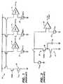
- FIG. 4Ashows an overall schematic diagram of an exemplary embodiment of a sense amplifier 100 for reading data stored in a memory cell or cell 105 according to the present invention.
- memory cell 105includes a field effect transistor (FET 110) having control-gate 115 and an isolated or floating-gate 120 that is electrically isolated from source 125 and drain 130 of the FET.
- FET 110field effect transistor
- Information or datais programmed or stored by injecting charge on the floating gate 120 to change the threshold voltage of the FET 110 from an intrinsic threshold voltage by an amount proportional to the charge.
- the programmed threshold voltage of FET 110represents one or more bits of programmed data.
- V REFa predetermined reference voltage
- Sense amplifier 100comprises a number of transistors that provide reference voltages and currents to cell 105, amplify a voltage signal that represents the programmed threshold voltage of the cell, and switch the coupling of some transistors to reconfigure the sense amplifier between different modes for completing different phases or cycles of operation.
- sense amplifier 105includes cascode device 135 coupled to drain 130 of FET 110 of cell 105.
- Cascode device 135increases resolution of sense amplifier 100, and isolates the remaining sense amplifier components from high-voltage developed on bit-line 140 during a write operation.
- cascode device 135is an FET 145 having source 150 coupled through bit-line 140 to drain 130 of the FET 110 of the memory cell 105 and to parasitic capacitance on the bit-line. This capacitance is represented by bit-line capacitor 155 connected in parallel with cell 105 to a source voltage V ss .
- the drain of FET 145 of cascode device 135is coupled through a first output node 160 to transistors 165, 170. These transistors 165, 170, are switched on to couple the cascode device to unity gain buffer 175 (not labeled in this figure) formed by a pair of differential transistors 180, 185, and transistors 190, 195, when sense amplifier 100 is operated in a pre-charge mode.
- drain 130 of cell 105 and node 160 of the cascode device 135are pre-charged to the predetermined reference voltage in preparation for reading the cell.
- the predetermined reference voltageis applied to a gate of transistor 185, and a gate of transistor 180 is coupled to node 160 to form a simple feedback circuit.
- Gates of transistors 190, 195,are coupled to one another through transistors 200, 205 and to a second output node (node 210) through transistors 215, 220.
- Transistor 225is coupled toVSS to provide bias current (I BIAS ) to unity gain buffer 175 through transistor 230.
- Transistor 235coupled to drain voltage V DD , provides reference current (I REF ) to node 160 through transistor 240, to which current through cell 105 is compared.
- I REF and I BIASare provided to node 160 to pre-charge the cell 105 to the predetermined reference voltage.
- I REFis on the order of a few ⁇ A, less than half of I BIAS .
- sense amplifier 100enables cell 105 to be pre-charged much more rapidly than does a conventional sense amplifier, which relies on a small pre-charge current namely I REF .
- a voltage(V OUT1 ) is allowed to develop on node 160.
- transistors 245, 250couple the gate of transistor 195 to a third output node (node 255).
- transistors 215, 220couple the gate of transistor 190 to node 210, and transistors 200, 205 couple the gates of transistors 190, 195, to one another.
- Transistors 245, 250also couple the gate of transistor 195 to node 255 in a regeneration mode, in which V OUT1 is compared to V REF to determine difference voltage (V DIFF ) representing data stored in cell 105.
- V DIFFdifference voltage
- gates of transistors 190, 195are coupled to node 210 and node 255 respectively to form a positive feedback loop.
- This configurationenables transistors 190, 195, to amplify V DIFF , thereby increasing resolution of sense amplifier 100.
- final stage 260comprising transistors 265, 270, 275 and 280, use control signal (cnt) applied to transistor 270 to pass the signals to output 285 only at the end of a regeneration step.
- FiGs. 4B - 4D, FIG. 5 and FIG. 6are simplified diagrams of the diagram of FIG. 4A showing sense amplifier 100 configured for pre-charge mode, develop mode, and regeneration mode respectively.
- FIG. 5is a timing diagram showing timing of control signals applied to components of sense amplifier 100 to configure it for different modes of operation.
- FIG. 6is a graph showing voltage waveforms from bit-line 140 and node 160 of sense amplifier 100 in different modes of operation.
- voltages refip, refin, vcg and vrefare established using reference circuits (not shown) and current mirrors (not shown).
- Voltage refipdetermines the effective comparison current, I COMP , and voltage refip establishes the bias current Ibias for the sense amplifier 100.
- Voltage vcgis applied to control-gate 115 to determine whether cell 105 threshold voltage is above or below vcg.
- Reference voltage blbiasis applied to the gate of the cascode device 135 to determine the voltage to which the bit-line 140 is charged during pre-charge mode.
- Voltage vrefis a reference voltage to which bit-line 140 and node 160 of the cascode device 135 is charged, and is typically chosen to be a predetermined value approximately halfway between the supply voltage and ground.
- FIG. 4Bshows sense amplifier 100 configured in the pre-charge mode.
- enable signals en and enbare applied to transistors 230 and 240 (shown in FIG. 4A) to enable sense amplifier 100.
- Control signals eq and eqbare applied to transistors 200, 205, to form unity gain buffer 175.
- Control signals prechrg and prechrgbare applied to transistors 165, 170, to couple unity gain buffer 175 to node 160 to pre-charge node 160 of cascode device 135 and bit-line 140 of cell 105.
- V REFis applied to transistor 185, the input of unity gain buffer 175, and cascode device 135 and drain 130 of cell 105 are pre-charged to the predetermined reference voltage.
- FIG. 4Cshows sense amplifier 100 configured in the develop mode.
- prechrg and prechrgbare removed from transistors 165, 170, (shown in FIG. 4A). This disconnects unity gain buffer 175 (shown in FIG. 4B) from node 160, and allows V OUT1 to develop on node 160.
- Transistors 165 and 170are preferably sized to minimize charge injection into node 160 at the beginning of the develop cycle when transistors 165 and 170 turn off. Minimizing charge injection is desired to improve the performance of the sense amplifier 100.
- V OUT1is improved by cascode device 135, because bit-line 140 capacitance (which is much bigger than the capacitance at node 160) needs to move by a small fraction of the V OUT1 change.
- differential transistors 180, 185are prepared for the next step, a regeneration operation, by shorting nodes 210 and 255, and connecting transistors 190,195, as a diode connected load.
- FIG. 5shows the control signals eq, eqb, regen and regenb applied to transistors 200, 205, 215, 245 and 250 respectively to accomplish this step.
- FIG. 4Dshows sense amplifier 100 configured in the regeneration mode.
- control signals eq and eqbare removed from transistors 200, 205, (shown in FIG. 4A) respectively decoupling the gates of transistors 190, 195.
- V OUT1will move by a very small amount in the develop operation.
- FIG. 6show how this is amplified in the regeneration operation. Referring to FIG. 6, line 290 indicates V OUT1 when I CELL is less than I REF , and line 295 indicates V OUT1 when I CELL is greater than I REF .
- V OUT1 and V REFV DIFF
- transistors 190, 195are configured to form an amplifier having a positive feedback loop to enable amplification of the change in V OUT1 from V REF . mode.
- nodes 210 and 255have digital levels indicating the result of comparison.
- control signal cntis applied to transistor 270 to pass the signals on nodes 210 and 255 to output 285.
- control signals eq, eqb, prechrg and prechrgbare applied to transistors 200, 205, 165 and 170, respectively, to reconfigure sense amplifier 100 for the next pre-charge operation.
- Control signals regen, regenb and cntare removed from transistors 245, 250 and 270 respectively.
- Enabling control signals en and enbare removed from transistors 230 and 240 respectively until the pre-charge operation is ready to begin.
- FIG. 7is a flowchart showing a process for operating the sense amplifier 100 according to an embodiment of the present invention.
- the processbegins by coupling the pre-charge circuit to the bit-line 140 through node 160 of cascode device 135 at step 305. Generally, this is accomplished by applying a control signal to the transistor switch to cause it to turn on.
- the cascode deviceis pre-charged to a predetermined reference voltage.
- the predetermined reference voltageis applied to the input of the unity gain buffer to generate a bias current (I BIAS ), and the I BIAS and a reference current (I REF ) from the reference current circuit are applied to the cascode device to pre-charge the cascode device to the predetermined reference voltage.
- the pre-charge circuitis de-coupled from the cascode device, step 315, and a voltage signal is developed representing data stored in the memory cell, at step 320.
- the step of developing the voltage signalis developed by allowing a difference between I REF and a current through the memory cell (I CELL ) to change the voltage to which the cascode device is charged.
- the pre-charge circuitis reconfigured as a regeneration circuit by changing the couplings between transistors in the pre-charge circuit to form an amplifier having a positive feedback loop.
- the voltage signalis then amplified using the regeneration circuit at step 330.
- sense amplifier 100an array of memory cells (not shown), a high-voltage supply or pump (not shown) and a selector (not shown) for selecting the cell to couple the sense amplifier to are fabricated on the same substrate or chip.
- sense amplifier 100 of the present inventioncan also be fabricated as a separate integrated circuit or as a circuit of separate components without departing from the scope of the present invention.
Landscapes
- Engineering & Computer Science (AREA)
- Computer Hardware Design (AREA)
- Microelectronics & Electronic Packaging (AREA)
- Read Only Memory (AREA)
- Amplifiers (AREA)
- Warehouses Or Storage Devices (AREA)
- Non-Volatile Memory (AREA)
Abstract
Description
- The present invention relates generally to non-volatile integrated memory devices and more particularly to an improved sense amplifier and method of operating the same to quickly read data stored in a multi-state memory cell with a high degree of accuracy.
- Non-volatile memories, such as electronically erasable programable read-only memories (EEPROM) or flash memories, are widely used in portable devices including devices lacking a mass data storage devices and a fixed source of power, such as cellular phones, handheld personal computers (PCs), portable music players and digital cameras.
- Non-volatile memories are typically semiconductor devices having a number of memory cells each with a field effect transistor having a control-gate and an isolated or floating-gate that is electrically isolated from a source and a drain of the FET. Non-volatile memories program or store information by injecting charge on the floating gate to change a threshold voltage of the FET. The injected charge changes the threshold voltage of the FET from an intrinsic threshold voltage by an amount proportional to the charge. The new threshold voltage of the FET in the memory cell represents one or more bits of programmed data or information. For example, in a simple memory cell storing a single bit of data, the FET threshold voltage is either raised to a value near a high end of the threshold voltage range or maintained at a value near a low end. These two programmed threshold voltages represent a logical one or a logical zero. These voltages program the memory cell to turn on or off, respectively, when read conditions are established, thereby enabling a read operation to determine if data stored in the memory cell is a logical one or a logical zero.
- To read the bit stored in a simple memory cell, an intermediate threshold voltage is applied to the FET and a resulting current compared with a reference current. A memory cell programmed to a high threshold voltage, a logical one, will conduct less current than the reference current, and a memory cell programmed to a low threshold voltage, a logical zero, will conduct more current than the reference current. The current comparison is accomplished with a circuit known as a sense amplifier or, more commonly, a sense amp. For a simple memory cell, the output of the sense amplifier is a one bit digital signal representing the logical state of the data stored in the memory cell.
- More sophisticated non-volatile memories have multilevel or multi-state memory cells enabling the storage of more than one bit per memory cell. Storing more than one bit per memory cell requires that the threshold voltage space of the memory cell be divided or partitioned into multiple regions or memory states, each associated with one of several threshold voltages representing one of several possible bits or data states. For example, a multi-state memory cell capable of storing two bits of data requires a threshold space having four memory states, and a multi-state memory cell storing three bits of data requires partitioning the threshold space into eight memory states. Exemplary flash memories having such multi-state memory cells are described in
U.S. Patents Nos. 5,043,940 and5,434,825 . - To exploit the concept of non-volatile memories having multi-state memory cells fully, the memory states should be packed as closely together as possible, with minimal threshold voltage separation for margin/discrimination overhead. Thus, reading a multi-slate memory cell requires that the sense amplifier precisely resolve the programmed threshold voltage with margins much smaller than the separation between available memory states. For example, given a multi-state memory cell having FETs with a two-volt threshold voltage space and four bits per memory cell (sixteen memory states per memory cell), each memory state is 125mV wide, which requires the sense amplifier to resolve threshold voltages to within a few millivolts. Typically, the sense amplifier must be able to resolve thresholds to within about 10 mV or less.
- In addition to resolving small voltage differences, performance requirements dictate that the sense amplifier be able to determine the programed threshold voltage within a very short time. This can be very critical in non-volatile memories using a closed loop write, where the programming operation is followed by a verify operation, in which the sense amplifier checks whether the threshold voltage of the memory cell being programmed has reached the desired value. These performance and resolution requirements are difficult to satisfy simultaneously. Often, performance must be sacrificed to improve resolution and vice versa.
- FIG. 1 shows a prior art sensing circuit, commonly known as a current sensing circuit. A
current mirroring circuit 10 andmultiple sense amplifiers 15, generally one sense amplifier for each memory state, compare the current frommemory cell 20 with multiple reference currents provided simultaneously by multiple referencecurrent circuits 25. A predetermined fixed voltage, higher than a maximum programmed threshold voltage, is applied to the control gate of the memory cell being read. The resultant memory cell current is mirrored using a P-channel FET to multiple P-channel FETs as shown in FIG. 1. These multiple mirrored currents are compared to multiple reference currents by the multiple sense amps. The different reference currents are equal to current produced by programmed threshold voltages that correspond to boundaries of threshold voltage partitions. The digital outputs of the sense amps indicate the memory cell state. - While an improvement over earlier designs, this approach is not wholly satisfactory for a number of reasons. As arrays grow in size and have increasing numbers of memory cells, it is not feasible to provide the necessary current, generally on the order of tens of micro amperes (µA), to mirror for the larger number of cells. Furthermore, it is difficult to read the cell state by distinguishing relatively small current levels.
- In a so-called voltage sensing approach, shown in FIGs. 2 and 3, a voltage (VBL) on a bit-
line 28 of thememory cell 20 is pre-charged to a reference voltage (VPRE) using a pre-charge voltage VPRE. Optionally, bit-line 28 of thememory cell 20 is pre-charged through acascode device 32. A control gate voltage (VCG) exceeding the maximum possible threshold voltage (VT) cell is applied to thecontrol gate 28. VCG is chosen in relation to VT such that an erased memory cell will always conduct with that magnitude of VCG. After a period of time, Δt, VBL is compared with a trip or reference voltage (VTRP) using an inverter orcomparator 30. Referring to FIG. 3, it is seen that if VBL is larger than VTRP after Δt, thecell 20 conducts less than an effective comparison current (ICOMP), and therefore VT is higher and the cell is programmed. It can be shown that a simplified approximate expression for the effective comparison current is:
where AV is the voltage gain of the cascode device, and CBL is the bit-line capacitance. - If the
memory cell 20 is a multilevel or multi-state memory cell, the VT can be determined more precisely by applying a sequence of different VCG voltages and comparing the resultant VBL voltages. For example, in one version of this approach known as half-stepping, a VCG of about half of a maximum possible VCG is applied. If the resultant VBL is less than VTRP, in a second iteration (or pass), a VCG that is half of the VCG applied in the first pass, or one-quarter of the maximum possible VCG is applied. If the resultant VBL is greater than expected, in the second or subsequent pass, a VCG that is 1.5 · VCG applied in the first pass, or 75% of the maximum possible VCG is applied. The process continues until the VT is determined with sufficient precision. - While an improvement over earlier designs and methods for large arrays and/or small devices, this approach is not wholly satisfactory. For example, the effective comparison current is generally not constant due to variation in supply voltage, develop time (the time in which the intermediate threshold voltage is developed), or time variations in bit-line capacitance, as ICOMP varies with time per the above equation. For example, bit-line capacitance can change from the write time to the read time of the cell due to write or erase of other memory cells in a memory array coupled to the same bit-line. This change in capacitance can cause an offset in ICOMP, resulting in multi-state memory cell data being read incorrectly.
- Another problem is that the difference between VPRE and VTRP can vary with temperature and with the voltage supply, especially when the comparator is a simple inverter. Further, measured time can vary due to variations in a clock chip (not shown), which is susceptible to variations in temperature and/or supply voltages.
US 5,581,511 , over which the independent claims are characterized, discloses a reading circuit for non-volatile memory cells in which the bit line and a reference line are pre-charged. Any differences in line voltage is eliminated before a voltage difference between the line indicative of a storage state of the memory cell is allowed to develop.- A further constraint on designs of non-volatile memories having multi-state memory cells is power consumed by the sense amplifier during the read operation. Non-volatile memories using the approach described above often require hundreds of sense amplifiers working in parallel to read the multi-state memory cells with sufficient precision and speed. Such large numbers of sense amplifiers can consume a significant portion of the available power. Thus, the very low power budgets of today's portable devices can put a severe constraint on sense amplifier design. For example, sense amps having cascode stages are desired for their increased gain. But cascode stages may not be practical because of an increased headroom required between voltage supply traces or head rails delivering high voltages from an external source. Non-volatile memories having high voltages from an on-chip voltage supply are available. However, these voltage supplies generally have a severely limited power capacity and consume too much power, especially in portable devices. Furthermore, the power available from on-chip voltage supplies is even more limited and must be conserved, especially to reduce chip heat dissipation. Thus, the shrinking power and voltage supplies in portable devices introduce limitations on sense amplifier designs.
- Another important consideration in the design of sense amps is the chip or die area used by the sense amplifier. As noted above, to achieve satisfactory performance, a non-volatile memory having multi-state memory cells typically requires multiple sense amps on the chip. Thus, sense amplifiers can make up a significant fraction of the die area of the non-volatile memory.
- Accordingly, there is a need for a non-volatile memory having multi-state memory cells with a sense amplifier capable of quickly reading data stored in the cell with a high degree of accuracy. There is a further need for a sense amplifier capable of reducing errors in reads due to due to low resolution. There is a still further need for a sense amplifier having a reduced power consumption, that makes efficient use of components to reduce cost and conserves chip space.
- The present invention provides such sense amplifiers.
- According to an aspect of the present invention there is provided a method of operating a sense amplifier as claimed in
claim 1. - According to another aspect of the present invention there is provided a memory device as claimed in claim 11.
- The preferred embodiment provides a sense amplifier with a pre-charged state set at the sense amplifier trip point. Use of such pre-charged trip point state provides an effective comparison current that is equal to a reference current, and substantially independent of variations in supply voltage, develop time, and capacitance of components of the sense amplifier, and advantageously reduces the time required for the sensing operation. In one embodiment, a pre-charge regenerative circuit is provided for the sense amplifier.
- A preferred embodiment provides a sense amplifier for reading data stored in a multi-state memory cell in a non-volatile memory device. The sense amplifier includes a cascode device coupled to the drain of the memory cell FET and having a pre-charge circuit coupled to the cascode device. The cascode device is preferably a FET having a source coupled to the drain of the memory cell FET and having a drain coupled to the pre-charge circuit. The cascode device increases the resolution of the sense amplifier during a read operation, and isolates other components of the sense amplifier from a high voltage applied to the memory cell during a write operation. The pre-charge circuit is configured to pre-charge a node of the cascode device. The cascode device pre-charges the bit-line coupled to the memory cell to a pre-charge state during a pre-charge operation when the sense amplifier is in a pre-charge mode. Such pre-charging advantageously reduces time required to read the multi-state memory cell.
- The pre-charge circuit includes a unity gain buffer to whose input a predetermined reference voltage is applied, and includes an output coupled to the node of the cascode device. The pre-charge circuit provides a bias current (IBIAS) to the cascode device to pre-charge the bit-line through the cascode device to the predetermined reference voltage. The pre-charge circuit can further include a transistor switch to couple the unity gain buffer to the cascode device when the sense amplifier is in the pre-charge mode, and to decouple it from the cascode device when the sense amplifier is in a develop mode. In develop mode, a reference current circuit provides a reference current (IREF) to the cascode device, and a difference between IREF and a current through the memory cell (lCELL) causes a change in the voltage applied to the cascode device from the predetermined reference voltage, thereby developing a voltage signal representing data stored in the memory cell.
- The pre-charge circuit is re-configured as a regeneration circuit when the sense amplifier is in a regeneration mode to amplify the voltage signal developed during the develop mode. The pre-charged state is selected to put the regeneration circuit into a meta-stable state set at a trip point of the sense amplifier. Use of such a pre-charged state at the trip point produces an effective comparison current that is equal to a reference current, and substantially independent from factors such as bit-line capacitance, supply voltage, and develop time. Such setting of the pre-charge state at the trip point of the sense amplifier can speed up the read operation.
- A method of operating a sense amplifier to read data stored in a multi-state memory cell is also provided. A pre-charge circuit is coupled to the cascode device, and the bit-line pre-charged through the cascode device to a predetermined reference voltage. The pre-charge circuit is de-coupled from the cascode device, and a voltage signal representing datastored in the memory cell is developed. The pre-charge circuit is reconfigured as a regeneration circuit to amplify the voltage signal.
- The pre-charge circuit includes a unity gain buffer having an output coupled to the cascode device through a transistor switch. Coupling the pre-charge circuit to the cascode device is accomplished by applying a control signal to turn-on the transistor switch. Pre-charging the bit-line through the cascode device to the predetermined reference voltage involves (i) applying the predetermined reference voltage to an input of the unity gain buffer, and (ii) applying a bias current IBIAS from the unity gain buffer to a node of the cascode device to pre-charge the bit-line to the predetermined reference voltage. The sense amplifier further includes a reference current circuit to provide a reference current (IREF) to the cascode device. The cascode device is pre-charged by applying both IREF and IBIAS simultaneously to the cascode device. Developing a voltage signal is accomplished by allowing a difference between IREF and a current through the memory cell (ICELL) to change the predetermined reference voltage to which the bit-line is charged.
- Reconfiguring the pre-charge circuit as a regeneration circuit involves forming an amplifier having a positive feedback loop. The voltage signal is then amplified using the amplifier. To further reduce time required to read the multi-state memory cell the pre-charge is preferably reconfigured to form the regeneration circuit while the voltage signal is being developed.
- These and various other features and advantages of the present invention will be apparent upon reading of the following detailed description in conjunction with the accompanying drawings, where:
- FIG. 1 is a schematic diagram of a read circuit for a non-volatile memory having multi-state memory cells comprising a current mirroring circuit and multiple sense amps, according to the prior art;
- FIG. 2 is a schematic diagram of another read circuit for a non-volatile memory having multi-state memory cells comprising a pre-charge circuit and voltage comparator, according to the prior art;
- FIG. 3 is a graph of voltage comparator output over time for the read circuit of FIG. 2, according to the prior art;
- FIG. 4A is a schematic diagram of a sense amplifier according to an embodiment of the present invention;
- FIG. 4B is a simplified schematic diagram of the sense amplifier of FIG. 4A configured in a pre-charge mode according to an embodiment of the present invention;
- FIG. 4C is a simplified schematic diagram of the sense amplifier of FIG. 4A configured in a develop mode according to an embodiment of the present invention;
- FIG. 4D is a simplified schematic diagram of the sense amplifier of FIG. 4A configured in a regeneration mode according to an embodiment of the present invention;
- FIG. 5 is a timing diagram showing timing of control signals applied to components of the sense amplifier to configure the sense amplifier for different modes of operation according to an embodiment of the present invention;
- FIG. 6 is a graph showing voltage waveforms from a sense amplifier according to an embodiment of the present invention; and
- FIG. 7 is a flowchart of a method for operating a sense amplifier according to the embodiment of the present invention.
- The present invention provides a sense amplifier for use in memories having multi-level memory cells that provides improved resolution and read times, and efficient use of components to reduce cost, immunity from process variation and' to conserve chip space. A sense amplifier used according to the present invention is particularly useful for use with multi-level or multi-state memory cells capable of storing multiple bits of data. For example, a multi-state memory cell capable of storing four bits of data and having a single FET with a two-volt threshold voltage space requires sixteen separate memory states (not shown), each 125mV wide. Thus, a sense amplifier used to read such a multi-state memory cell would require a high resolution to distinguish between the different memory states. Sense amplifier and the method of the preferred embodiments provide a resolution of at least about ± 5mV.
- The sense amplifier will now be described with reference to FIGs. 4A to 4D. FIG. 4A shows an overall schematic diagram of an exemplary embodiment of a
sense amplifier 100 for reading data stored in a memory cell orcell 105 according to the present invention. - Referring to FIG. 4A,
memory cell 105 includes a field effect transistor (FET 110) havingcontrol-gate 115 and an isolated or floating-gate 120 that is electrically isolated fromsource 125 and drain 130 of the FET. Information or data is programmed or stored by injecting charge on the floatinggate 120 to change the threshold voltage of theFET 110 from an intrinsic threshold voltage by an amount proportional to the charge. The programmed threshold voltage ofFET 110 represents one or more bits of programmed data. - To read data stored in
cell 105, a predetermined reference voltage (VREF) is applied to drain 130 ofFET 110. A resulting current, sunk by the cell, is compared to a reference current to determine the programmed threshold voltage of the cell, and thereby the state of data stored in the cell. Sense amplifier 100 comprises a number of transistors that provide reference voltages and currents tocell 105, amplify a voltage signal that represents the programmed threshold voltage of the cell, and switch the coupling of some transistors to reconfigure the sense amplifier between different modes for completing different phases or cycles of operation.- Referring again to FIG. 4A,
sense amplifier 105 includescascode device 135 coupled to drain 130 ofFET 110 ofcell 105.Cascode device 135 increases resolution ofsense amplifier 100, and isolates the remaining sense amplifier components from high-voltage developed on bit-line 140 during a write operation. In the embodiment shown,cascode device 135 is anFET 145 havingsource 150 coupled through bit-line 140 to drain 130 of theFET 110 of thememory cell 105 and to parasitic capacitance on the bit-line. This capacitance is represented by bit-line capacitor 155 connected in parallel withcell 105 to a source voltage Vss. - The drain of
FET 145 ofcascode device 135 is coupled through afirst output node 160 totransistors transistors differential transistors transistors sense amplifier 100 is operated in a pre-charge mode. In the pre-charge mode, drain 130 ofcell 105 andnode 160 of thecascode device 135 are pre-charged to the predetermined reference voltage in preparation for reading the cell. The predetermined reference voltage is applied to a gate oftransistor 185, and a gate oftransistor 180 is coupled tonode 160 to form a simple feedback circuit. Gates oftransistors transistors transistors Transistor 225 is coupled toVSS to provide bias current (IBIAS) tounity gain buffer 175 throughtransistor 230. Transistor 235, coupled to drain voltage VDD, provides reference current (IREF) tonode 160 throughtransistor 240, to which current throughcell 105 is compared. In the pre-charge mode, IREF and IBIAS are provided tonode 160 to pre-charge thecell 105 to the predetermined reference voltage. Generally, IREF is on the order of a few µA, less than half of IBIAS. Thus,sense amplifier 100 enablescell 105 to be pre-charged much more rapidly than does a conventional sense amplifier, which relies on a small pre-charge current namely IREF.- In a develop mode, a voltage (VOUT1) is allowed to develop on
node 160. In thismode transistors transistor 195 to a third output node (node 255). At the same time,transistors transistor 190 tonode 210, andtransistors transistors Transistors transistor 195 tonode 255 in a regeneration mode, in which VOUT1 is compared to VREF to determine difference voltage (VDIFF) representing data stored incell 105. In the regeneration mode, gates oftransistors node 210 andnode 255 respectively to form a positive feedback loop. This configuration enablestransistors sense amplifier 100. Using thesame transistors sense amplifier 100. During different sense amplifier modes ofoperation node 210 andnode 255 go through intermediate voltages, signals taken from these nodes cannot be used directly in digital logic circuits. Therefore,final stage 260, comprisingtransistors transistor 270 to pass the signals tooutput 285 only at the end of a regeneration step.- Operation of
sense amplifier 100 in different modes of operation will now be described in more detail with reference to FiGs. 4B - 4D, FIG. 5 and FIG. 6. FiGs. 4B, 4C and 4D are simplified diagrams of the diagram of FIG. 4A showingsense amplifier 100 configured for pre-charge mode, develop mode, and regeneration mode respectively. FIG. 5 is a timing diagram showing timing of control signals applied to components ofsense amplifier 100 to configure it for different modes of operation. FIG. 6 is a graph showing voltage waveforms from bit-line 140 andnode 160 ofsense amplifier 100 in different modes of operation. - Before the sensing operation begins, voltages refip, refin, vcg and vref are established using reference circuits (not shown) and current mirrors (not shown). Voltage refip determines the effective comparison current, ICOMP, and voltage refip establishes the bias current Ibias for the
sense amplifier 100. Voltage vcg is applied to control-gate 115 to determine whethercell 105 threshold voltage is above or below vcg. Reference voltage blbias, is applied to the gate of thecascode device 135 to determine the voltage to which the bit-line 140 is charged during pre-charge mode. Voltage vref is a reference voltage to which bit-line 140 andnode 160 of thecascode device 135 is charged, and is typically chosen to be a predetermined value approximately halfway between the supply voltage and ground. - FIG. 4B shows
sense amplifier 100 configured in the pre-charge mode. Referring to FIG. 4B and FIG. 5, at time t0 enable signals en and enb are applied totransistors 230 and 240 (shown in FIG. 4A) to enablesense amplifier 100. Control signals eq and eqb are applied totransistors unity gain buffer 175. Control signals prechrg and prechrgb are applied totransistors unity gain buffer 175 tonode 160 topre-charge node 160 ofcascode device 135 and bit-line 140 ofcell 105. VREF is applied totransistor 185, the input ofunity gain buffer 175, andcascode device 135 and drain 130 ofcell 105 are pre-charged to the predetermined reference voltage. Note that if current through cell 105 (ICELL) is greater than IREF + IBIAS, then it will not be possible to chargecascode device 135 and drain 130 of the cell to VREF. However, this will not affect operation ofsense amplifier 100, whose output will still indicate thatcell 105 is conducting more current than IREF in the develop mode. - FIG. 4C shows
sense amplifier 100 configured in the develop mode. Referring to FIG. 4C and FIG. 5, after the pre-charge operation is complete, at time t1 control signals prechrg and prechrgb are removed fromtransistors node 160, and allows VOUT1 to develop onnode 160.Transistors node 160 at the beginning of the develop cycle whentransistors sense amplifier 100. If significant charge is injected tonode 160, the node voltage can change, and the develop cycle must be made larger to recover from such injected charge. The voltage onnode 160 will drop from the pre-charged value, VREF if ICELL is greater than IREF, and will increase if ICELL is smaller than IREF. The change in VOUT1 is improved bycascode device 135, because bit-line 140 capacitance (which is much bigger than the capacitance at node 160) needs to move by a small fraction of the VOUT1 change. While VOUT1 is being developed,differential transistors nodes transistors - FIG. 4D shows
sense amplifier 100 configured in the regeneration mode. Referring to FIG. 4D and FIG. 5, after the develop operation is complete, at time t2 control signals eq and eqb are removed fromtransistors transistors line 290 indicates VOUT1 when ICELL is less than IREF, andline 295 indicates VOUT1 when ICELL is greater than IREF. This small difference between VOUT1 and VREF (VDIFF) is amplified in the regeneration mode bytransistors transistors nodes transistor 270 to pass the signals onnodes output 285. - At time t4 control signals eq, eqb, prechrg and prechrgb are applied to
transistors sense amplifier 100 for the next pre-charge operation. Control signals regen, regenb and cnt are removed fromtransistors transistors - A method or process of operating the
sense amplifier 100 to read a memory having multi-level memory cells will now be described. FIG. 7 is a flowchart showing a process for operating thesense amplifier 100 according to an embodiment of the present invention. The process begins by coupling the pre-charge circuit to the bit-line 140 throughnode 160 ofcascode device 135 atstep 305. Generally, this is accomplished by applying a control signal to the transistor switch to cause it to turn on. Next, atstep 310, the cascode device is pre-charged to a predetermined reference voltage. The predetermined reference voltage is applied to the input of the unity gain buffer to generate a bias current (IBIAS), and the IBIAS and a reference current (IREF) from the reference current circuit are applied to the cascode device to pre-charge the cascode device to the predetermined reference voltage. The pre-charge circuit is de-coupled from the cascode device,step 315, and a voltage signal is developed representing data stored in the memory cell, atstep 320. Atstep 320, the step of developing the voltage signal is developed by allowing a difference between IREF and a current through the memory cell (ICELL) to change the voltage to which the cascode device is charged. Atstep 325, the pre-charge circuit is reconfigured as a regeneration circuit by changing the couplings between transistors in the pre-charge circuit to form an amplifier having a positive feedback loop. The voltage signal is then amplified using the regeneration circuit atstep 330. - Preferably,
sense amplifier 100, an array of memory cells (not shown), a high-voltage supply or pump (not shown) and a selector (not shown) for selecting the cell to couple the sense amplifier to are fabricated on the same substrate or chip. However, it will be understood thatsense amplifier 100 of the present invention can also be fabricated as a separate integrated circuit or as a circuit of separate components without departing from the scope of the present invention. - It is to be understood that even though numerous characteristics and advantages of certain embodiments of the present invention have been set forth in the foregoing description, together with details of the structure and function of various embodiments of the invention, this disclosure is illustrative only. Changes may be made as to detail, especially in matters of structure and arrangement of parts within the principles of the present invention to the full extent indicated by the broad general meaning of the terms in which the appended claims are expressed. For example, although the preferred embodiment described herein is directed to memories using solid-state microelectronics, it will be appreciated by those skilled in the art that the teachings of the present invention can be adapted to other memories, for example those using molecular-scale organic or chemical switches. Thus, the scope of the appended claims is not to be limited to the preferred embodiments described herein.

Claims (20)
- A method of operating a sense amplifier (100) to read data stored in a memory cell (105), the method comprising steps of:pre-charging a bit-line (140) of the memory cell (105) from a discharged state to a pre-determined reference voltage substantially equal to a trip point of the sense amplifier (100) using a pre-charging circuit;developing a voltage signal representing data stored in the memory cell (105);reconfiguring the pre-charge circuit as a regeneration circuit; andamplifying the voltage signal using the regeneration circuit;CHARACTERISED IN THAT:the pre-charge circuit comprises a unity gain buffer (175) having an output connected to the bit-line (140) and an input connected to a voltage supply that is maintained at the predetermined reference voltage throughout the pre-charging of the bit-line (140).
- A method according to Claim 1, further including the step of pre-charging a node (160) of a cascode device (135) coupled to the bit-line of the memory cell.
- A method according to Claim 2 further comprising the steps of:coupling the pre-charge circuit to the cascode device (135) prior to the pre-charging; anddecoupling the pre-charge circuit from the cascode device (135) after the pre-charging.
- A method according to Claim 3, wherein the unity gain buffer (175) has an output switchably coupled to the cascode device (135) and wherein the step of coupling the pre-charge circuit to the cascode device (135) includes applying a control signal to couple the output to the cascode device (135).
- A method according to Claim 4, wherein the step of pre-charging the cascode device (135) to a predetermined reference voltage further includes applying a bias current from the unity gain buffer (175) to the cascode device (135) to pre-charge the bit-line (140) of the memory cell (105) by charging the node (160) of the cascode device (135) to the predetermined reference voltage.
- A method according to Claim 5, wherein the sense amplifier (100) further comprises a reference current circuit to provide a reference current to the cascode device (135), and wherein the step of pre-charging the cascode device (135) to a predetermined reference voltage includes applying the reference current and the bias current simultaneously to the cascode device (135) to pre-charge the bit-line (140) through the cascode device (135) to the predetermined reference voltage.
- A method according to Claim 6, wherein the step of developing a voltage signal includes enabling a difference between the reference current and a current through the memory cell to cause a change from the predetermined reference voltage to which the cascode device (135) is charged.
- A method according to any preceding claim, wherein the step of reconfiguring the pre-charge circuit as a regeneration circuit includes forming an amplifier having a positive feedback loop.
- A method according to Claim 8, wherein forming the amplifier includes using components comprising the unity gain buffer (175).
- A method according to Claim 8 or Claim 9, wherein the step of amplifying the voltage signal includes amplifying the voltage signal using the amplifier.
- A memory device comprising:a plurality of multi-state memory cells (105), an individual memory cell having a field effect transistor (110) with a source (125) and a drain (130) that is connected to a bit-line (140); anda sense amplifier (100) comprising:a cascode device (135) coupled to the drain of the field effect transistor (110) of the memory cell (105), the cascode device (135) adapted to increase the resolution of the sense amplifier (100) during a read mode and to isolate the sense amplifier (100) from a high voltage applied to the memory cell (105) during a write mode; anda pre-charge circuit coupled to the cascode device (135), the pre-charge circuit configured to pre-charge the bit-line (140) of the memory cell (105) through the cascode device (135) during a pre-charge mode to reduce time required to read the multi-state memory cell,CHARACTERISED IN THAT:the pre-charge circuit comprises a unity gain buffer (175) having an output coupled to the cascode device (135) and an input, the pre-charge circuit arranged so that a predetermined reference voltage is applied to the input of the unity gain buffer as the bit-line (140) is pre-charged from a discharge state, and so that the output provides a bias current to the cascode device (135) to pre-charge the bit-line (140) by charging a node (160) of the cascode device (135) to the predetermined reference voltage.
- A memory device according to Claim 11, wherein the cascode device (135) is coupled in series between the pre-charge circuit and the drain (130) of the field effect transistor (110) in the memory cell (105).
- A memory device according to Claim 11 or Claim 12, wherein the pre-charge circuit further comprises a transistor switch (165, 170) to couple the unity gain buffer (175) to the cascode device (135) during the pre-charge mode and to de-couple the unity gain buffer (175) from the cascode device (135) during a develop mode.
- A memory device according to Claim 13 further comprising a reference current circuit to provide a reference current, wherein in the develop mode a difference between the reference current and a current through the memory cell causes a change from the predetermined reference voltage to which the node of the cascode device (135) is charged to develop a voltage signal representing data stored in the memory cell (105).
- A memory device according to Claim 14, wherein the pre-charge circuit is re-configurable as a regeneration circuit during a regeneration mode to amplify the voltage signal developed during the develop mode.
- A memory device according to any one of Claims 11 to 15, further comprising a high-voltage supply for writing data to the multi-state memory cells (105).
- The memory device of any one of Claims 11 to 16, further comprising:means for developing a voltage signal representing data stored in the memory cell (105); andmeans for amplifying the voltage signal.
- A memory device according to Claim 17, wherein the means for developing a voltage signal comprises:means for decoupling the output of the pre-charge circuit from the cascode device (135); anda reference current circuit to provide a reference current to the cascode device (135);wherein a difference between the reference current and a current through the memory cell causes a change from the predetermined reference voltage to which the node (160) of the cascode device (135) is charged.
- A memory device according to Claim 17 or Claim 18, wherein the means for amplifying the voltage signal comprises a regeneration circuit having an amplifier with a positive feedback loop.
- A memory device according to Claim 19, wherein the pre-charging circuit comprises components of the unity gain buffer (175) coupled together in a first configuration and wherein the regeneration circuit comprises components of the unity gain buffer (175) coupled together in a second configuration.
Applications Claiming Priority (3)
| Application Number | Priority Date | Filing Date | Title |
|---|---|---|---|
| US989996 | 2001-11-20 | ||
| US09/989,996US6747892B2 (en) | 2000-11-21 | 2001-11-20 | Sense amplifier for multilevel non-volatile integrated memory devices |
| PCT/US2002/036356WO2003044803A2 (en) | 2001-11-20 | 2002-11-12 | Sense amplifier for multilevel non-volatile integrated memory devices |
Publications (3)
| Publication Number | Publication Date |
|---|---|
| EP1446807A2 EP1446807A2 (en) | 2004-08-18 |
| EP1446807A4 EP1446807A4 (en) | 2005-11-30 |
| EP1446807B1true EP1446807B1 (en) | 2008-01-16 |
Family
ID=25535640
Family Applications (1)
| Application Number | Title | Priority Date | Filing Date |
|---|---|---|---|
| EP02799188AExpired - LifetimeEP1446807B1 (en) | 2001-11-20 | 2002-11-12 | Sense amplifier for multilevel non-volatile integrated memory devices |
Country Status (9)
| Country | Link |
|---|---|
| US (1) | US6747892B2 (en) |
| EP (1) | EP1446807B1 (en) |
| JP (1) | JP4274943B2 (en) |
| KR (1) | KR100915883B1 (en) |
| CN (1) | CN100456389C (en) |
| AT (1) | ATE384330T1 (en) |
| AU (1) | AU2002364118A1 (en) |
| DE (1) | DE60224703T2 (en) |
| WO (1) | WO2003044803A2 (en) |
Families Citing this family (35)
| Publication number | Priority date | Publication date | Assignee | Title |
|---|---|---|---|---|
| JP3709846B2 (en)* | 2002-01-18 | 2005-10-26 | ソニー株式会社 | Parallel AD converter |
| EP1915759B1 (en)* | 2005-07-04 | 2018-09-19 | Micron Technology, Inc. | Low power multiple bit sense amplifier |
| US7656710B1 (en) | 2005-07-14 | 2010-02-02 | Sau Ching Wong | Adaptive operations for nonvolatile memories |
| US7385848B2 (en)* | 2005-09-09 | 2008-06-10 | Sharp Kabushiki Kaisha | Semiconductor storage device and electronic equipment |
| US7489546B2 (en)* | 2005-12-20 | 2009-02-10 | Micron Technology, Inc. | NAND architecture memory devices and operation |
| JP4855773B2 (en)* | 2005-12-26 | 2012-01-18 | 株式会社東芝 | Semiconductor memory device and data read method thereof |
| US7457178B2 (en)* | 2006-01-12 | 2008-11-25 | Sandisk Corporation | Trimming of analog voltages in flash memory devices |
| US7254071B2 (en)* | 2006-01-12 | 2007-08-07 | Sandisk Corporation | Flash memory devices with trimmed analog voltages |
| US7525855B2 (en)* | 2006-04-24 | 2009-04-28 | Sandisk Corporation | Method of high-performance flash memory data transfer |
| US7366029B2 (en)* | 2006-04-24 | 2008-04-29 | Sandisk Corporation | High-performance flash memory data transfer |
| US7499369B2 (en)* | 2006-07-19 | 2009-03-03 | Sandisk Corporation | Method of high-performance flash memory data transfer |
| US7499339B2 (en)* | 2006-07-19 | 2009-03-03 | Sandisk Corporation | High-performance flash memory data transfer |
| US7345926B2 (en)* | 2006-04-24 | 2008-03-18 | Sandisk Corporation | High-performance flash memory data transfer |
| US7366028B2 (en) | 2006-04-24 | 2008-04-29 | Sandisk Corporation | Method of high-performance flash memory data transfer |
| JPWO2007125590A1 (en) | 2006-04-28 | 2009-09-10 | スパンション エルエルシー | Semiconductor device and control method thereof |
| US7809994B2 (en)* | 2006-05-17 | 2010-10-05 | Sandisk Corporation | Error correction coding for multiple-sector pages in flash memory devices |
| US20070300130A1 (en)* | 2006-05-17 | 2007-12-27 | Sandisk Corporation | Method of Error Correction Coding for Multiple-Sector Pages in Flash Memory Devices |
| US7355892B2 (en)* | 2006-06-30 | 2008-04-08 | Sandisk Corporation | Partial page fail bit detection in flash memory devices |
| US7304893B1 (en) | 2006-06-30 | 2007-12-04 | Sandisk Corporation | Method of partial page fail bit detection in flash memory devices |
| CN100580806C (en)* | 2006-10-12 | 2010-01-13 | 旺宏电子股份有限公司 | Memory and low offset limiting bias circuit thereof |
| US7522463B2 (en) | 2007-01-12 | 2009-04-21 | Atmel Corporation | Sense amplifier with stages to reduce capacitance mismatch in current mirror load |
| US7508715B2 (en)* | 2007-07-03 | 2009-03-24 | Sandisk Corporation | Coarse/fine program verification in non-volatile memory using different reference levels for improved sensing |
| US7599224B2 (en)* | 2007-07-03 | 2009-10-06 | Sandisk Corporation | Systems for coarse/fine program verification in non-volatile memory using different reference levels for improved sensing |
| US7746713B2 (en)* | 2007-09-12 | 2010-06-29 | Massachusetts Institute Of Technology | High density 45 nm SRAM using small-signal non-strobed regenerative sensing |
| JP5490432B2 (en)* | 2008-03-17 | 2014-05-14 | ピーエスフォー ルクスコ エスエイアールエル | Semiconductor device |
| US7710782B2 (en)* | 2008-05-05 | 2010-05-04 | Macronix International Co., Ltd. | Sense amplifier and data sensing method thereof |
| CN101609710B (en)* | 2008-06-17 | 2011-07-27 | 旺宏电子股份有限公司 | Sense amplifier circuit and data sensing method thereof |
| US8469971B2 (en)* | 2008-08-12 | 2013-06-25 | Boston Scientific Neuromodulation Corporation | Stylet for guiding leads of implantable electric stimulation systems and methods of making and using |
| US8509013B1 (en)* | 2010-04-30 | 2013-08-13 | Micron Technology, Inc. | Partitioned bitline for memory |
| US9047930B2 (en)* | 2013-07-26 | 2015-06-02 | International Business Machines Corporation | Single-ended low-swing power-savings mechanism with process compensation |
| CN105469818B (en)* | 2014-09-12 | 2018-01-26 | 上海华虹宏力半导体制造有限公司 | sense amplifier |
| US9997250B2 (en) | 2016-03-17 | 2018-06-12 | SK Hynix Inc. | Non-volatile memory device with a plurality of cache latches and switches and method for operating non-volatile memory device |
| KR102424285B1 (en)* | 2018-02-01 | 2022-07-25 | 에스케이하이닉스 주식회사 | Multi level sensing circuit and semiconductor device including the same |
| US11372056B2 (en)* | 2020-05-26 | 2022-06-28 | Sandisk Technologies Llc | Circuit for detecting pin-to-pin leaks of an integrated circuit package |
| US12094542B2 (en) | 2020-12-08 | 2024-09-17 | Stmicroelectronics International N.V. | Device and method to generate bias voltages in non-volatile memory |
Family Cites Families (13)
| Publication number | Priority date | Publication date | Assignee | Title |
|---|---|---|---|---|
| US5268319A (en)* | 1988-06-08 | 1993-12-07 | Eliyahou Harari | Highly compact EPROM and flash EEPROM devices |
| US5095344A (en)* | 1988-06-08 | 1992-03-10 | Eliyahou Harari | Highly compact eprom and flash eeprom devices |
| US5172338B1 (en) | 1989-04-13 | 1997-07-08 | Sandisk Corp | Multi-state eeprom read and write circuits and techniques |
| US5220531A (en) | 1991-01-02 | 1993-06-15 | Information Storage Devices, Inc. | Source follower storage cell and improved method and apparatus for iterative write for integrated circuit analog signal recording and playback |
| US6222762B1 (en) | 1992-01-14 | 2001-04-24 | Sandisk Corporation | Multi-state memory |
| FR2694119B1 (en)* | 1992-07-24 | 1994-08-26 | Sgs Thomson Microelectronics | Reading circuit for memory, with recharging and balancing before reading. |
| US5591384A (en) | 1994-03-31 | 1997-01-07 | Modern Technologies Corp. | Method for molding parts |
| EP0735542A1 (en) | 1995-03-31 | 1996-10-02 | STMicroelectronics S.r.l. | Reading circuit for multilevel non-volatile memory cell devices |
| US5684736A (en) | 1996-06-17 | 1997-11-04 | Nuram Technology, Inc. | Multilevel memory cell sense amplifier system |
| US6490200B2 (en) | 2000-03-27 | 2002-12-03 | Sandisk Corporation | Non-volatile memory with improved sensing and method therefor |
| IT1314042B1 (en)* | 1999-10-11 | 2002-12-03 | St Microelectronics Srl | MEMORY READING AMPLIFIER CIRCUIT, WITH HIGH CAPACITY OF DISCRIMINATION OF CURRENT LEVELS. |
| KR100436127B1 (en)* | 2000-06-28 | 2004-06-14 | 주식회사 하이닉스반도체 | semiconductor memory device having sense amplifier and method for driving sense amplifier |
| US6538922B1 (en) | 2000-09-27 | 2003-03-25 | Sandisk Corporation | Writable tracking cells |
- 2001
- 2001-11-20USUS09/989,996patent/US6747892B2/ennot_activeExpired - Lifetime
- 2002
- 2002-11-12ATAT02799188Tpatent/ATE384330T1/ennot_activeIP Right Cessation
- 2002-11-12JPJP2003546354Apatent/JP4274943B2/ennot_activeExpired - Fee Related
- 2002-11-12AUAU2002364118Apatent/AU2002364118A1/ennot_activeAbandoned
- 2002-11-12DEDE60224703Tpatent/DE60224703T2/ennot_activeExpired - Lifetime
- 2002-11-12CNCNB028230825Apatent/CN100456389C/ennot_activeExpired - Fee Related
- 2002-11-12KRKR1020047007706Apatent/KR100915883B1/ennot_activeExpired - Fee Related
- 2002-11-12WOPCT/US2002/036356patent/WO2003044803A2/enactiveIP Right Grant
- 2002-11-12EPEP02799188Apatent/EP1446807B1/ennot_activeExpired - Lifetime
Also Published As
| Publication number | Publication date |
|---|---|
| AU2002364118A1 (en) | 2003-06-10 |
| KR20040070174A (en) | 2004-08-06 |
| EP1446807A4 (en) | 2005-11-30 |
| ATE384330T1 (en) | 2008-02-15 |
| WO2003044803A3 (en) | 2003-08-28 |
| EP1446807A2 (en) | 2004-08-18 |
| US6747892B2 (en) | 2004-06-08 |
| JP2005510006A (en) | 2005-04-14 |
| DE60224703T2 (en) | 2009-01-08 |
| CN100456389C (en) | 2009-01-28 |
| JP4274943B2 (en) | 2009-06-10 |
| DE60224703D1 (en) | 2008-03-06 |
| KR100915883B1 (en) | 2009-09-07 |
| US20030095431A1 (en) | 2003-05-22 |
| WO2003044803A2 (en) | 2003-05-30 |
| CN1672215A (en) | 2005-09-21 |
Similar Documents
| Publication | Publication Date | Title |
|---|---|---|
| EP1446807B1 (en) | Sense amplifier for multilevel non-volatile integrated memory devices | |
| US11031050B2 (en) | Power line compensation for flash memory sense amplifiers | |
| US5729492A (en) | Sense amplifier having capacitively coupled input for offset compensation | |
| JP4344769B2 (en) | Low voltage memory sensing circuit and method | |
| CN101346773B (en) | Reference sense amplifier and method for compensated sensing in non-volatile memory | |
| US6788601B2 (en) | Semiconductor memory device and current mirror circuit | |
| US7453742B2 (en) | Semiconductor integrated circuit device | |
| EP3114688B1 (en) | Improved sensing circuits for use in low power nanometer flash memory devices | |
| EP0907955B1 (en) | A multiple bits-per-cell flash shift register page buffer | |
| US8213234B2 (en) | Current sink system for source-side sensing | |
| CN101105976A (en) | Method and apparatus for reading data from non-volatile memory | |
| EP1966801B1 (en) | Reference sense amplifier and method for compensated sensing in non-volatile memory | |
| JP4237337B2 (en) | Apparatus and method for reading non-volatile memory cells | |
| US7158431B2 (en) | Single transistor sensing and double transistor sensing for flash memory | |
| US5889699A (en) | Non-volatile semiconductor memory device | |
| EP1324344B1 (en) | Sense amplifier structure for multilevel non-volatile memory devices and corresponding reading method | |
| US6240018B1 (en) | Nonvolatile semiconductor memory device having verify function | |
| US7751251B2 (en) | Current sensing scheme for non-volatile memory | |
| EP1011105B1 (en) | One-chip microcomputer | |
| US20020122336A1 (en) | Reference voltage generation the circuit for semiconductor memory device, memory reading circuit including same, and electronic information device including the same | |
| US6603681B2 (en) | Method of pulse programming, in particular for high-parallelism memory devices, and a memory device implementing the method | |
| JP2008077766A (en) | Semiconductor device |
Legal Events
| Date | Code | Title | Description |
|---|---|---|---|
| PUAI | Public reference made under article 153(3) epc to a published international application that has entered the european phase | Free format text:ORIGINAL CODE: 0009012 | |
| 17P | Request for examination filed | Effective date:20040519 | |
| AK | Designated contracting states | Kind code of ref document:A2 Designated state(s):AT BE BG CH CY CZ DE DK EE ES FI FR GB GR IE IT LI LU MC NL PT SE SK TR | |
| AX | Request for extension of the european patent | Extension state:AL LT LV MK RO SI | |
| A4 | Supplementary search report drawn up and despatched | Effective date:20051019 | |
| GRAP | Despatch of communication of intention to grant a patent | Free format text:ORIGINAL CODE: EPIDOSNIGR1 | |
| GRAS | Grant fee paid | Free format text:ORIGINAL CODE: EPIDOSNIGR3 | |
| GRAA | (expected) grant | Free format text:ORIGINAL CODE: 0009210 | |
| AK | Designated contracting states | Kind code of ref document:B1 Designated state(s):AT BE BG CH CY CZ DE DK EE ES FI FR GB GR IE IT LI LU MC NL PT SE SK TR | |
| RAP1 | Party data changed (applicant data changed or rights of an application transferred) | Owner name:SANDISK CORPORATION | |
| REG | Reference to a national code | Ref country code:GB Ref legal event code:FG4D | |
| REG | Reference to a national code | Ref country code:CH Ref legal event code:EP | |
| REG | Reference to a national code | Ref country code:IE Ref legal event code:FG4D | |
| REF | Corresponds to: | Ref document number:60224703 Country of ref document:DE Date of ref document:20080306 Kind code of ref document:P | |
| PG25 | Lapsed in a contracting state [announced via postgrant information from national office to epo] | Ref country code:LI Free format text:LAPSE BECAUSE OF FAILURE TO SUBMIT A TRANSLATION OF THE DESCRIPTION OR TO PAY THE FEE WITHIN THE PRESCRIBED TIME-LIMIT Effective date:20080116 Ref country code:ES Free format text:LAPSE BECAUSE OF FAILURE TO SUBMIT A TRANSLATION OF THE DESCRIPTION OR TO PAY THE FEE WITHIN THE PRESCRIBED TIME-LIMIT Effective date:20080427 Ref country code:FI Free format text:LAPSE BECAUSE OF FAILURE TO SUBMIT A TRANSLATION OF THE DESCRIPTION OR TO PAY THE FEE WITHIN THE PRESCRIBED TIME-LIMIT Effective date:20080116 Ref country code:CH Free format text:LAPSE BECAUSE OF FAILURE TO SUBMIT A TRANSLATION OF THE DESCRIPTION OR TO PAY THE FEE WITHIN THE PRESCRIBED TIME-LIMIT Effective date:20080116 | |
| REG | Reference to a national code | Ref country code:CH Ref legal event code:PL | |
| PG25 | Lapsed in a contracting state [announced via postgrant information from national office to epo] | Ref country code:BG Free format text:LAPSE BECAUSE OF FAILURE TO SUBMIT A TRANSLATION OF THE DESCRIPTION OR TO PAY THE FEE WITHIN THE PRESCRIBED TIME-LIMIT Effective date:20080416 Ref country code:AT Free format text:LAPSE BECAUSE OF FAILURE TO SUBMIT A TRANSLATION OF THE DESCRIPTION OR TO PAY THE FEE WITHIN THE PRESCRIBED TIME-LIMIT Effective date:20080116 | |
| ET | Fr: translation filed | ||
| PG25 | Lapsed in a contracting state [announced via postgrant information from national office to epo] | Ref country code:PT Free format text:LAPSE BECAUSE OF FAILURE TO SUBMIT A TRANSLATION OF THE DESCRIPTION OR TO PAY THE FEE WITHIN THE PRESCRIBED TIME-LIMIT Effective date:20080616 Ref country code:BE Free format text:LAPSE BECAUSE OF FAILURE TO SUBMIT A TRANSLATION OF THE DESCRIPTION OR TO PAY THE FEE WITHIN THE PRESCRIBED TIME-LIMIT Effective date:20080116 | |
| PG25 | Lapsed in a contracting state [announced via postgrant information from national office to epo] | Ref country code:DK Free format text:LAPSE BECAUSE OF FAILURE TO SUBMIT A TRANSLATION OF THE DESCRIPTION OR TO PAY THE FEE WITHIN THE PRESCRIBED TIME-LIMIT Effective date:20080116 Ref country code:SK Free format text:LAPSE BECAUSE OF FAILURE TO SUBMIT A TRANSLATION OF THE DESCRIPTION OR TO PAY THE FEE WITHIN THE PRESCRIBED TIME-LIMIT Effective date:20080116 Ref country code:CZ Free format text:LAPSE BECAUSE OF FAILURE TO SUBMIT A TRANSLATION OF THE DESCRIPTION OR TO PAY THE FEE WITHIN THE PRESCRIBED TIME-LIMIT Effective date:20080116 Ref country code:SE Free format text:LAPSE BECAUSE OF FAILURE TO SUBMIT A TRANSLATION OF THE DESCRIPTION OR TO PAY THE FEE WITHIN THE PRESCRIBED TIME-LIMIT Effective date:20080416 | |
| PLBE | No opposition filed within time limit | Free format text:ORIGINAL CODE: 0009261 | |
| STAA | Information on the status of an ep patent application or granted ep patent | Free format text:STATUS: NO OPPOSITION FILED WITHIN TIME LIMIT | |
| 26N | No opposition filed | Effective date:20081017 | |
| PG25 | Lapsed in a contracting state [announced via postgrant information from national office to epo] | Ref country code:EE Free format text:LAPSE BECAUSE OF FAILURE TO SUBMIT A TRANSLATION OF THE DESCRIPTION OR TO PAY THE FEE WITHIN THE PRESCRIBED TIME-LIMIT Effective date:20080116 | |
| PG25 | Lapsed in a contracting state [announced via postgrant information from national office to epo] | Ref country code:MC Free format text:LAPSE BECAUSE OF NON-PAYMENT OF DUE FEES Effective date:20081130 | |
| GBPC | Gb: european patent ceased through non-payment of renewal fee | Effective date:20081112 | |
| PG25 | Lapsed in a contracting state [announced via postgrant information from national office to epo] | Ref country code:CY Free format text:LAPSE BECAUSE OF FAILURE TO SUBMIT A TRANSLATION OF THE DESCRIPTION OR TO PAY THE FEE WITHIN THE PRESCRIBED TIME-LIMIT Effective date:20080116 | |
| PG25 | Lapsed in a contracting state [announced via postgrant information from national office to epo] | Ref country code:IT Free format text:LAPSE BECAUSE OF NON-PAYMENT OF DUE FEES Effective date:20081112 | |
| PG25 | Lapsed in a contracting state [announced via postgrant information from national office to epo] | Ref country code:IE Free format text:LAPSE BECAUSE OF NON-PAYMENT OF DUE FEES Effective date:20081112 | |
| PG25 | Lapsed in a contracting state [announced via postgrant information from national office to epo] | Ref country code:GB Free format text:LAPSE BECAUSE OF NON-PAYMENT OF DUE FEES Effective date:20081112 | |
| PG25 | Lapsed in a contracting state [announced via postgrant information from national office to epo] | Ref country code:LU Free format text:LAPSE BECAUSE OF NON-PAYMENT OF DUE FEES Effective date:20081112 | |
| PG25 | Lapsed in a contracting state [announced via postgrant information from national office to epo] | Ref country code:TR Free format text:LAPSE BECAUSE OF FAILURE TO SUBMIT A TRANSLATION OF THE DESCRIPTION OR TO PAY THE FEE WITHIN THE PRESCRIBED TIME-LIMIT Effective date:20080116 | |
| PG25 | Lapsed in a contracting state [announced via postgrant information from national office to epo] | Ref country code:GR Free format text:LAPSE BECAUSE OF FAILURE TO SUBMIT A TRANSLATION OF THE DESCRIPTION OR TO PAY THE FEE WITHIN THE PRESCRIBED TIME-LIMIT Effective date:20080417 | |
| REG | Reference to a national code | Ref country code:NL Ref legal event code:SD Effective date:20111229 | |
| REG | Reference to a national code | Ref country code:FR Ref legal event code:TP Owner name:SANDISK TECHNOLOGIES INC., US Effective date:20120229 | |
| REG | Reference to a national code | Ref country code:DE Ref legal event code:R082 Ref document number:60224703 Country of ref document:DE Representative=s name:PATENTANWAELTE MAXTON LANGMAACK & PARTNER, DE | |
| REG | Reference to a national code | Ref country code:DE Ref legal event code:R081 Ref document number:60224703 Country of ref document:DE Owner name:SANDISK TECHNOLOGIES INC., PLANO, US Free format text:FORMER OWNER: SANDISK CORP., MILPITAS, CALIF., US Effective date:20120713 Ref country code:DE Ref legal event code:R082 Ref document number:60224703 Country of ref document:DE Representative=s name:PATENTANWAELTE MAXTON LANGMAACK & PARTNER, DE Effective date:20120713 Ref country code:DE Ref legal event code:R082 Ref document number:60224703 Country of ref document:DE Representative=s name:PATENTANWAELTE LIPPERT, STACHOW & PARTNER, DE Effective date:20120713 Ref country code:DE Ref legal event code:R081 Ref document number:60224703 Country of ref document:DE Owner name:SANDISK TECHNOLOGIES LLC, PLANO, US Free format text:FORMER OWNER: SANDISK CORP., MILPITAS, CALIF., US Effective date:20120713 Ref country code:DE Ref legal event code:R082 Ref document number:60224703 Country of ref document:DE Representative=s name:LIPPERT STACHOW PATENTANWAELTE RECHTSANWAELTE , DE Effective date:20120713 | |
| PGFP | Annual fee paid to national office [announced via postgrant information from national office to epo] | Ref country code:NL Payment date:20121110 Year of fee payment:11 | |
| PGFP | Annual fee paid to national office [announced via postgrant information from national office to epo] | Ref country code:FR Payment date:20131108 Year of fee payment:12 | |
| REG | Reference to a national code | Ref country code:NL Ref legal event code:V1 Effective date:20140601 | |
| PG25 | Lapsed in a contracting state [announced via postgrant information from national office to epo] | Ref country code:NL Free format text:LAPSE BECAUSE OF NON-PAYMENT OF DUE FEES Effective date:20140601 | |
| REG | Reference to a national code | Ref country code:DE Ref legal event code:R082 Ref document number:60224703 Country of ref document:DE Representative=s name:PATENTANWAELTE LIPPERT, STACHOW & PARTNER, DE Ref country code:DE Ref legal event code:R082 Ref document number:60224703 Country of ref document:DE Representative=s name:LIPPERT STACHOW PATENTANWAELTE RECHTSANWAELTE , DE | |
| REG | Reference to a national code | Ref country code:FR Ref legal event code:ST Effective date:20150731 | |
| PG25 | Lapsed in a contracting state [announced via postgrant information from national office to epo] | Ref country code:FR Free format text:LAPSE BECAUSE OF NON-PAYMENT OF DUE FEES Effective date:20141201 | |
| REG | Reference to a national code | Ref country code:DE Ref legal event code:R082 Ref document number:60224703 Country of ref document:DE Representative=s name:PATENTANWAELTE LIPPERT, STACHOW & PARTNER, DE Ref country code:DE Ref legal event code:R081 Ref document number:60224703 Country of ref document:DE Owner name:SANDISK TECHNOLOGIES LLC, PLANO, US Free format text:FORMER OWNER: SANDISK TECHNOLOGIES INC., PLANO, TEX., US Ref country code:DE Ref legal event code:R082 Ref document number:60224703 Country of ref document:DE Representative=s name:LIPPERT STACHOW PATENTANWAELTE RECHTSANWAELTE , DE | |
| PGFP | Annual fee paid to national office [announced via postgrant information from national office to epo] | Ref country code:DE Payment date:20171108 Year of fee payment:16 | |
| REG | Reference to a national code | Ref country code:DE Ref legal event code:R119 Ref document number:60224703 Country of ref document:DE | |
| PG25 | Lapsed in a contracting state [announced via postgrant information from national office to epo] | Ref country code:DE Free format text:LAPSE BECAUSE OF NON-PAYMENT OF DUE FEES Effective date:20190601 |