EP1443332A1 - Current sensor and current sensor manufacturing method - Google Patents
Current sensor and current sensor manufacturing methodDownload PDFInfo
- Publication number
- EP1443332A1 EP1443332A1EP02775480AEP02775480AEP1443332A1EP 1443332 A1EP1443332 A1EP 1443332A1EP 02775480 AEP02775480 AEP 02775480AEP 02775480 AEP02775480 AEP 02775480AEP 1443332 A1EP1443332 A1EP 1443332A1
- Authority
- EP
- European Patent Office
- Prior art keywords
- current
- magnetic field
- magnetic
- detection element
- field detection
- Prior art date
- Legal status (The legal status is an assumption and is not a legal conclusion. Google has not performed a legal analysis and makes no representation as to the accuracy of the status listed.)
- Granted
Links
Images


Classifications
- G—PHYSICS
- G01—MEASURING; TESTING
- G01R—MEASURING ELECTRIC VARIABLES; MEASURING MAGNETIC VARIABLES
- G01R15/00—Details of measuring arrangements of the types provided for in groups G01R17/00 - G01R29/00, G01R33/00 - G01R33/26 or G01R35/00
- G01R15/14—Adaptations providing voltage or current isolation, e.g. for high-voltage or high-current networks
- G01R15/20—Adaptations providing voltage or current isolation, e.g. for high-voltage or high-current networks using galvano-magnetic devices, e.g. Hall-effect devices, i.e. measuring a magnetic field via the interaction between a current and a magnetic field, e.g. magneto resistive or Hall effect devices
- G01R15/202—Adaptations providing voltage or current isolation, e.g. for high-voltage or high-current networks using galvano-magnetic devices, e.g. Hall-effect devices, i.e. measuring a magnetic field via the interaction between a current and a magnetic field, e.g. magneto resistive or Hall effect devices using Hall-effect devices
- G—PHYSICS
- G01—MEASURING; TESTING
- G01R—MEASURING ELECTRIC VARIABLES; MEASURING MAGNETIC VARIABLES
- G01R31/00—Arrangements for testing electric properties; Arrangements for locating electric faults; Arrangements for electrical testing characterised by what is being tested not provided for elsewhere
- G—PHYSICS
- G01—MEASURING; TESTING
- G01R—MEASURING ELECTRIC VARIABLES; MEASURING MAGNETIC VARIABLES
- G01R15/00—Details of measuring arrangements of the types provided for in groups G01R17/00 - G01R29/00, G01R33/00 - G01R33/26 or G01R35/00
- G01R15/14—Adaptations providing voltage or current isolation, e.g. for high-voltage or high-current networks
- G01R15/20—Adaptations providing voltage or current isolation, e.g. for high-voltage or high-current networks using galvano-magnetic devices, e.g. Hall-effect devices, i.e. measuring a magnetic field via the interaction between a current and a magnetic field, e.g. magneto resistive or Hall effect devices
- G01R15/207—Constructional details independent of the type of device used
- H—ELECTRICITY
- H01—ELECTRIC ELEMENTS
- H01L—SEMICONDUCTOR DEVICES NOT COVERED BY CLASS H10
- H01L2224/00—Indexing scheme for arrangements for connecting or disconnecting semiconductor or solid-state bodies and methods related thereto as covered by H01L24/00
- H01L2224/01—Means for bonding being attached to, or being formed on, the surface to be connected, e.g. chip-to-package, die-attach, "first-level" interconnects; Manufacturing methods related thereto
- H01L2224/42—Wire connectors; Manufacturing methods related thereto
- H01L2224/47—Structure, shape, material or disposition of the wire connectors after the connecting process
- H01L2224/48—Structure, shape, material or disposition of the wire connectors after the connecting process of an individual wire connector
- H01L2224/4805—Shape
- H01L2224/4809—Loop shape
- H01L2224/48091—Arched
- H—ELECTRICITY
- H01—ELECTRIC ELEMENTS
- H01L—SEMICONDUCTOR DEVICES NOT COVERED BY CLASS H10
- H01L2224/00—Indexing scheme for arrangements for connecting or disconnecting semiconductor or solid-state bodies and methods related thereto as covered by H01L24/00
- H01L2224/01—Means for bonding being attached to, or being formed on, the surface to be connected, e.g. chip-to-package, die-attach, "first-level" interconnects; Manufacturing methods related thereto
- H01L2224/42—Wire connectors; Manufacturing methods related thereto
- H01L2224/47—Structure, shape, material or disposition of the wire connectors after the connecting process
- H01L2224/48—Structure, shape, material or disposition of the wire connectors after the connecting process of an individual wire connector
- H01L2224/481—Disposition
- H01L2224/48151—Connecting between a semiconductor or solid-state body and an item not being a semiconductor or solid-state body, e.g. chip-to-substrate, chip-to-passive
- H01L2224/48221—Connecting between a semiconductor or solid-state body and an item not being a semiconductor or solid-state body, e.g. chip-to-substrate, chip-to-passive the body and the item being stacked
- H01L2224/48245—Connecting between a semiconductor or solid-state body and an item not being a semiconductor or solid-state body, e.g. chip-to-substrate, chip-to-passive the body and the item being stacked the item being metallic
- H01L2224/48247—Connecting between a semiconductor or solid-state body and an item not being a semiconductor or solid-state body, e.g. chip-to-substrate, chip-to-passive the body and the item being stacked the item being metallic connecting the wire to a bond pad of the item
Definitions
- the present inventionrelates to a current sensor and a method of manufacturing the current sensor.
- the present inventionrelates to a current sensor of magnetoelectric conversion type, which measures the intensity of a current by detecting a flux generated by the current to be measured with a magnetic field detection element, and a manufacturing method thereof.
- a Hall sensor using the Hall effect, a magnetoresistive element, a magnetic transistor, etcare widely known as magnetic sensors. Capturing a magnetic flux created around a current to be measured and measuring its current intensity can be done by using such magnetic field sensors.
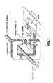
- a current sensor structure shown in Fig. 1is widely used conventionally.
- the current sensor having the configuration of Fig. 1is not suitable for miniaturization because the sensor requires a magnetic core 4 surrounding a current conductor 2 fed with current. Further, since the magnetic core 4 and a Hall element 6 need to be separately manufactured and then assembled into one, the sensor has not been suitable for mass production and the cost is not low.
- a magnetic field sensor with a terminal for detecting currentcontaining a chip with a magnetoelectric conversion element sealed with plastics
- This publicationdiscloses "a magnetic field sensor with a terminal for detecting current.
- This magnetic field sensorcomprises a current conductor, a magnetoelectric conversion element chip placed on a part of the above current conductor (except both sides of the conductor), lead frames (each side of which are connected to the chip) and a sealing part (for integrally sealing the end of the lead frame, the magnetoelectric conversion element chip, and the part of the chip located on a current conductor).
- This magnetic field sensoris characterized in that the sensor has both ends of the current conductor as external terminals for current detection".
- the present inventionprovides a low-cost current sensor suitable for mass production and a manufacturing method, the current sensor is small with high sensitivity and can be packaged in a standard assembly line which is normally used for manufacturing an integrated circuit.
- Another object of the present inventionis to provide a current sensor which is packaged in a standard assembly line with sufficient shielding effect against a disturbance flux, and to provide a manufacturing method thereof.
- a current sensorwhich comprises a magnetic field detection element placed on a current conductor passedby acurrent to be measured, wherein the magnetic field detection element is placed close to a flux concentrator for converging a flux generated by the current to be measured, and wherein an input/output terminal of the magnetic field detection element is placed on the same height of a plane compared to that of the current conductor or is placed on a plane which has a predetermined height difference compared to that of the current conductor.
- the flux concentratorin the first claim of the current sensor, may be composed of a pair of members having a gap between them.
- the current sensor in the first claimmay further comprise a first magnetic material on the backside of the current conductor, on which side the magnetic field detection element is not located.
- the current sensor in the third claimmay further comprise a second magnetic material above the current conductor, on which side the magnetic field detection element is located.
- a position of the second magnetic materialmay be set so as to satisfy 0.1 ⁇ X ⁇ 3.6 ⁇ where ⁇ represents a whole length of the flux concentrator along a direction of a flux generated by the current to be measured and X represents a distance between a magnetic detecting surface of the magnetic field detection element and the second magnetic material.
- the detection sensitivity of the magnetic field detection elementis substantially increased by reducing a width of the current conductor where the magnetic field detection element is placed on.
- a method of manufacturing a current sensorwhich comprises a magnetic field detection element on a current conductor passed by a current to be measured, wherein the magnetic field detection element is placed close to a flux concentrator for converging a flux generated by the current to be measured, and wherein an input/output terminal of the magnetic field detection element is placed on the same height of a plane compared to that of the current conductor oris placedon a plane which has a predetermined height difference compared to that of the current conductor, the manufacturing method comprising the steps of:
- a method of manufacturing a current sensorwhich comprises a magnetic field detection element on a current conductor passed by a current to be measured, wherein the magnetic field detection element is placed close to a flux concentrator for converging a flux generated by the current to be measured, and wherein an input/output terminal of the magnetic field detection element is placed on the same height of a plane compared to that of the current conductor oris placed on a plane which has a predetermined height difference compared to that of the current conductor, the manufacturing method comprising the steps of:
- a method of manufacturing a current sensorwhich comprises a magnetic field detection element placed on a current conductor passed by a current to be measured, wherein the magnetic field detection element is placed close to a flux concentrator for converging a flux generated by the current to be measured, and wherein an input/output terminal of the magnetic field detection element is placed on the same height of a plane compared to that of the current conductor oris placed on a plane which has a predetermined height difference compared to that of the current conductor, the manufacturing method comprising the steps of:
- a position of the second magnetic materialmay be set so as to satisfy 0.1 ⁇ X ⁇ 3.6 ⁇ where ⁇ represents a whole length of the flux concentrator along a direction of a flux generated by the current to be measured and X represents a distance between a magnetic detecting surface of the magnetic field detection element and the second magnetic material.
- the detection sensitivity of the magnetic field detection elementis substantially increased by reducing a width of the current conductor where the magnetic field detection element is placed on.
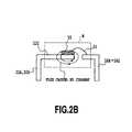
- Fig. 2Ais a perspective view showing schematically the entire configuration of a current sensor employing the present invention.
- Fig. 2Bis a view showing schematically the configuration of the current sensor shown in Fig. 2A.
- reference numeral 20denotes a magnetic field sensor chip including a magnetic field detection element like a Hall element and so on
- reference numerals 22A to 22Cdenote current conductors for applying a current to be measured
- reference numerals 24A to 24Ddenote lead frame terminals.
- Each of the lead frame terminals 24A to 24D and the current conductor 22A to 22Care formed from a single thin plate-like metal as will be discussed later (Fig. 4A and Fig. 4B) .
- Reference numeral 26denotes a bonding wire for connecting the lead frame terminals 24A to 24D and the magnetic field sensor chip 20.
- reference character Mdenotes a part to be molded in plastics.
- Figs. 3A, 3B, and 3Care, respectively, a perspective view, a sectional view, and a surface view showing the detail of a magnetic field sensor chip 20 shown in Fig. 2A.
- the magnetic field sensor chip 20is entirely placed on the current conductor 22C and detects the magnitude of an induction field generated by the current to be measured.
- two flux concentrators 28A and 28Bare placed having a predetermined interval between them.
- Two Hall elements 30A and 30Bare placed on a region which is placed below the two flux concentrators 28A and 28B where flux density is high (that is, on the side of the sensor chip substrate 32),
- an induction field caused by the current to be measuredpasses through the magnetic field sensor chip 20 in such a way that the induction field passes though the flux concentrator 28A, the Hall element 30A, the other Hall element 30B, and the other flux concentrator 28B.
- the illustrated magnetic field sensor chip 20itself has been disclosed in US Patent Publication (USP No. 5,942,895: "MAGNETIC FIELD SENSOR AND CURRENT AND/OR ENERGY SENSOR", Popovic et al.) by the inventor of the present application. With the provision of the magnetic field sensor chip 20, it is possible to efficiently detect a flux looped around a surface of a current conductor (in parallel with the surface of the current conductor), thereby achieving a current sensor with high sensitivity.
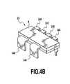
- Figs. 4A and 4Bare views for explaining a manufacturing process of the magnetic field sensor chip 20 shown in Figs. 2A, 2B, 3A, 3B, and 3C.
- a plural set of the current conductor 22A to 22C and lead frame terminals 24A to 24Dis formed at one at the same time by etching or pressing a single thin plate-like metal.
- a processed thin piece metal which is cut out for one chip regionhas an appearance shown in Fig. 4B in the end.
- the external view of Fig. 4Bis identical to Fig. 2A (perspective view) , which has been already discussed.
- the current conductor 22C passed by the current to be measuredis configured so as to have the same height position of a plane compared to that of the lead frame terminals 24A to 24D, with which the terminals of the magnetic field sensor chip are connected. Or in order to perform wire bonding readily, the surface of the current conductor 22C where the magnetic field sensor chip 20 is placed on can be pressed down by approximately a thickness of the chip.
- the conductive material passed through by the current and the lead frame terminalscan be formed as one at the same time from a single flat plate-like material by using a method such as etching and /or pressing. This method achieves mass-productivity at low cost.
- FIG. 4AA copper plate with a thickness of 0.4 mm was used as a thin plate-like metal (Fig. 4A) to form the current conductor 22A to 22C and the lead frame terminals 24A to 24D as one.
- Fig. 4Ashows that a plurality of chips are connected. Manufacturing in large quantity was readily performed by using completely the same process used for lead frames of a typical integrated circuit. Then the above lead frames were used to form a current sensor molded in plastics used for an integrated circuit. This is shown in Fig. 4B.
- the width of the center part 22C of the current conductor placing the magnetic field sensor chip 20 thereonwas about 2 mm, and the outside of the molded plastics was about 5.5 mm in width, and a maximum current of 25A could be applied continuously.
- the Hall ASIC shown in Figs. 3B and 3Cwas applied on the magnetic field sensor chip 20.
- the Hall ASICwas fixed on an island of the current conductor by an insulating adhesive tape used for die bonding of an integrated circuit.
- the Hall ASIChad a pair of flux concentrators (soft magnetic material thin film-like) 28A and 28B which were separated by a gap, and Hall elements were placed directly below each flux concentrator.
- flux concentratorssoft magnetic material thin film-like
- the fluxpasses through the flux concentrator 28A on the surface of the ASIC chip, draws an arc-shaped trail over the gap of the flux concentrators, penetrates the Hall elements placed directly below the flux concentrators, and is absorbed by the other flux concentrator 28B.
- electromotive forceis generated corresponding to a flux density. Since the flux density is proportional to the intensity of the current passing through the current conductor, an electromotive force proportional to the intensity of the flowing current is generated at the Hall elements, and the intensity of the current can be detected.
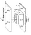
- Figs. 5A and 5Bare schematical perspective views showing the entire configuration of a current sensor corresponding to another embodiment.
- a soft thin plate-like magnetic material 50is bonded beneath a current conductor 22C (that is, bonded on the opposite side from a magnetic field sensor chip 20).
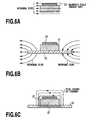
- Figs. 6A, 6B, and 6Care explanatory drawings showing the function of the soft, thin plate-like magnetic material 50 shown in Figs. 5A and 5B.
- the soft, thin plate-like magnetic material 50 with high magnetic permeability, high saturation flux density, and low coercive forceis bonded on the backside of an island part 22C of the current conductor, so that the soft, thin plate-like magnetic material 50 absorbs an external flux entering from the outside of the current sensor, and that it passes through the plate 50.
- the soft, thin plate-like magnetic material 50also converges and amplifies a flux generated by the current to be measured, and thus, further improve the sensitivity of the current sensor.
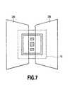
- the two Hall elements 30A and 30Bare placed below the two flux concentrators 28A and 28B.
- a single Hall element 70may be placed instead of the two Hall elements 30A and 30B.
- the single Hall element 70is placed over two flux concentrators 28A and 28B and a gap between the concentrators in this case.
- a magnetic field sensor chipis not restricted to employ a Hall element as long as preferable sensitivity is realized for a horizontal flux to a surface of the chip.
- a magnetoresistive element or GMRis also applicable for it.
- a soft, thin plate-like magnetic material 50was 0.35 mm in thickness, 10 mm in length, and 7 mm in width. Then, the thin plate was bonded on the backside of a current conductor using an insulating adhesive tape which is used for bonding Hall ASIC chip onto an island described above. As a result, as compared to the case where the soft magnetic material thin plate 50 is not bonded, the sensitivity to current to be measured was improved by about 1.8 times, and the sensitivity to an external flux of Figs. 6A and 6B was reduced to about one eighth.
- Fig. 8Ais a schematical perspective view showing the entire configuration of a current sensor corresponding to embodiment 3.
- a second magnetic material (shield plate) 51is placed above a magnetic field sensor chip 20 which is placed on an island 22C of a current conductor, in addition to the configuration of Fig. 5A.
- Fig. 8Bis an explanatory drawing showing the function of the second magnetic material 51 shown in Fig. 8A.
- the magnetic material (shield plate) with high magnetic permeability, high saturation flux density, and low coercive forceis placed over the magnetic field sensor chip 20, so that a disturbance flux coming from the outside is absorbed by the second magnetic material 51 (shield plate) and passes through the material 51.
- a disturbance flux coming from the outsideis absorbed by the second magnetic material 51 (shield plate) and passes through the material 51.
- Fig. 8Ba representation indicating the magnetic shielding effect caused by the first magnetic material 50 (cf. Fig. 6B) protecting a current sensor from a disturbance flux is not depicted.
- Figs. 9 and 10are explanatory drawings emphasizing the main parts of embodiment 3. Properly speaking, Figs. 9 and 10 depict a section view cut in centers, but character references C and G denote a whole length of a magnetic plate (which is twice the length from a center to an edge).
- a placement of the magnetic detection surface of a magnetic field detection element using Hall elements or the likeis substantially the same height position of the bottoms of the flux concentrators.
- a distance between the position (the magnetic detection surface of a magnetic field detection element) and the bottom of the second magnetic material 51is X.
- a total length of the flux concentrators including two flux concentrators 28A, 28B and a gapis ⁇ along the flowing direction of a measuring magnetic field generated by the current to be measured.
- a region satisfying 0.1 ⁇ X ⁇ 3.6 ⁇is effective.
- the singular regionis practically an area satisfying the above condition, 0.1 ⁇ X ⁇ 3.6 ⁇ .
- measuring magnetic fieldforms a magnetic path passing through the first magnetic material and the magnetic concentrator.
- the second magnetic material(shield plate) 51draws an external disturbance (interference) magnetic flux mainly, rather than the measuring flux caused by the current to be measured.
- a placement of the first magnetic material 50 and the second magnetic material 51is not restricted to the inside of the molded resin. These may be placed inside or outside of the molded resin, or on the surface of it.
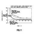
- Fig. 11shows numerical analysis results indicating magnetic shielding effect of the embodiment shown in Figs. 8A, 8B, 9, and 10, when a disturbance current wire is moved vertically over the current sensor.
- the disturbance current wirewas placed above the second magnetic material 51 so as to cross above the center of the magnetic field sensor chip, and moved vertically. This case brings the largest disturbance to a magnetic field to be measured.
- the horizontal axis of Fig. 11represents a distance X (unit: mm) between the center of the disturbance current wire and the magnetic detection surface of the Hall element. A distance between a package surface and the Hall element was calculated based on a design size determined when the package was prototyped.
- the vertical axis of Fig. 11represents an output deviation (%).
- the detecting sensitivity [mV/A] with no disturbance and the detecting sensitivity [mV/A] corresponding to a distance to the disturbance current wirewere computed, and "deviation of sensor outputs" resulting from an disturbance flux were computed based on the calculated detection sensitivities.
- a commercial magnetic field analysis toolwas used for the numerical analysis. It was assumed that ideal DC line current flows in the disturbance current wire. Then, for both cases where disturbance is absent and present, a flux crossing the magnetic detection surface of a Hall element was computed by the numerical analysis, an average flux density over the magnetic detection surface was computed as post processing, and "deviation of sensor outputs" resulting from disturbance were computed based on the results.
- a width L of the current conductor, total length ⁇ of two concentrators with an air gap, and sizes E and F of the second magnetic material closely placed to the magnetic sensor chip 20 containing the magnetic concentrator,are important to form a magnetic path between the flux concentrator and the first magnetic material.
- a magnetic field analysisis done on distance X for each combination of L, ⁇ , E, F.
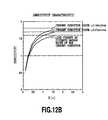
- Figs. 12A, 12B, and 12Cshow sensitivity curves which are computed by a magnetic field analysis tool using a magnetic circuit model employed for the numerical calculation of Fig. 11.
- sensitivity characteristicsis shown in Fig 12A for sizes (width E, thickness F) of the second magnetic material 51, and is shown in Fig.12B for the width L of the current conductor, and is shown in Fig 12C for a total length ⁇ of the flux concentrator with a gap(cf. Fig. 10).
- the horizontal axisrepresents a distance X (unit: ⁇ ) between the bottom (or base) of the second magnetic material 51 and the magnetic detection surface of the Hall elements.
- the vertical axisrepresents relative sensitivity for distance X on (an assumption that sensitivity is 1 when the first magnetic material 50 and the second magnetic material 51 are absent (Embodiment 1: Fig. 2A).
- the sensitivity characteristics of this caseare indicated by a solid line.
- a dotted line on relative sensitivity of 1corresponds to "embodiment 1”
- a dotted line around relative sensitivity of 1.8corresponds to "embodiment 2”.
- the width Eincreases, absolute sensitivity tends to decrease.
- the changeis very small (not shown in Fig.12A).
- the detection sensitivityis 1 when X is about 0.23 ⁇ .
- Xwas 0.681 ⁇ and the detection sensitivity was 1.53.
- Fig. 12Bshows sensitivity characteristics when the current conductor decreases in width.
- Horizontal scaleis distance X.
- Sensitivity for each width L of the current conductor in embodiment 1is used as standard value of "1".
- Fig. 12Cshows sensitivity characteristics when the entire length ⁇ of the flux concentrator is increased.
- ⁇3.04 mm.
- the width B0.115 ⁇ (0.35 mm)
- the length C3.289 ⁇ (10 mm)
- a magnetic field analysiswas done using the magnetic circuit model applied in the numerical analysis as shown in Fig.11.
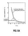
- Fig. 13A, 13B and 13Cshow the results.
- the disturbance current wireis placed in a constant position, about 22 mm far away from the magnetic detection surface, and the second magnetic material 51 is vertically moved between the magnetic field sensor chip 20 and the disturbance current wire.
- the horizontal axisrepresents a distance X (unit: ⁇ ) between the base(bottom) of the second magnetic material 51 and the magnetic detection surface of the Hall elements.
- the vertical axisrepresents the relative sensitivity for each case.
- the horizontal axisis a distance X.
- a flux density (that is, sensitivity) passing through the magnetic detection surface of the Hall element in "embodiment 2 which comprises the first magnetic material 50is as standard value of "1" (Figs. 5A and 5B)".
- the relative sensitivityie.
- Sensor sensitivityis based on a density of a flux passing through the magnetic detection surface of the magnetic field detection element (a flux density , that is sensitivity, in "embodiment 2" is treated as “1" ).
- the flux density on the magnetic detection surfaceis computed as a combined value of a disturbance flux generated by disturbance current and a measuring magnetic field generated by the current to be measured. If the second magnetic material is very close to the magnetic detection surface, a drawing phenomenon of a flux caused by the second magnetic material 51, that is, an intake effect of a flux appears markedly. At this moment, a flux does not go mainly toward the magnetic detection surface.
- Fig. 13Bshows the magnetic shielding effect when the width of the current conductor is reduced.
- the thickness F0.201 ⁇ (0.35 mm)
- the length G5.747 ⁇ (10 mm)
- the width E4.022 ⁇ (7 mm).
- Fig. 13Bthe relative sensitivities for each current width are indicated by solid lines and a dotted line on the same drawing, wherein the flux density (sensitivity) in embodiment 2 for each current width is "1".
- the horizontal axisis the distance.
- the solid line with * marksindicates the characteristics of the ideal line current.
- Fig. 13Cshows a magnetic shielding effect which appears when the entire length ⁇ of the flux concentrator is enlarged.
- the position of the disturbance current wireis positioned in constant about 22mm above the magnetic detection surface of the Hall elements.
- Fig. 13Crelative sensitivity is indicated by a solid line and a dotted line, wherein sensitivity for each ⁇ in embodiment 2 is treated as standard value of "1".
- Horizontal axisis the distance X.
- the horizontal axisdenotes the real size of ⁇ in mm units, and the vertical axis is exppresed as upper or lower limit of a singular region in unit ⁇ .
- the lower limit of Xis 0.1 ⁇ . If ⁇ becomes larger, lower limit of X becomes less than 0.1 ⁇ . If ⁇ becomes more large, lower limit of X tends to close to zero. If ⁇ becomes smaller, lower limit of X becomes more than 0.23 ⁇ .
- the two Hall elements 30A and 30Bare placed below the two flux concentrators 28A and 28B in the embodiment 3 described above.
- a single Hall element 70may be placed instead of the two Hall elements 30A and 30B.
- the single Hall element 70is placed over the two flux concentrators 28A and 28B and a gap between the concentrators.
- the single Hall element 70 of Fig. 7has been disclosed in US Patent Publication (USP No. 5, 942, 895: "MAGNETIC FIELD SENSOR AND CURRENT AND/OR ENERGY SENSOR", Popovic et al.) by the inventor of the present application.
- the sensor chipis not restricted to employ the Hall element as long as preferable sensitivity is obtained for a horizontal flux to a chip surface.
- a magnetoresistive elementis also applicable as magnetic detection element.
- Fig. 14shows an example of the top view of a current sensor.
- Fig. 14shows that the magnetic detection part containing the magnetic flux concentrators 28A and 28B and a gap is indicated by reference numeral 20, and that a width E of a second magnetic material 51 is indicated by reference numeral 81, a length G of it is indicated by reference numeral 82, and that a whole length ⁇ of the magnetic detecting part 20 containing the magnetic flux concentrators 28A and 28B and a gap is depicted in reference numeral 85, and a length of numeral reference 20 toward current flow is depicted in numeral number 86.
- the dimensions of the first magnetic material 50are omitted.
- reference numeral 85 indicating a width ⁇ of the magnetic detection part containing the flux concentrators 28A and 28B and a gapwas ranged from 1.74 to 3.04 mm.
- the two magnetic materials 50 and 51 placed above and below the magnetic field sensor chip 20are not restricted each other to the same shape and size mentioned so far. Further, each of a shape of the magnetic materials 50 and 51 is not restricted to a single thin plate-like shape (rectangular and parallelepiped).
- the essence of the present inventionis a configuration for sandwiching a current conductor 22C and the magnetic field sensor chip 20 with, at least, the two magnetic materials 50 and 51 in proper positions.
- the present embodimentmakes it possible to achieve a reasonable measuring sensitivity and an enough magnetic shielding effect while taking a balance of them.
- a distance X between the second magnetic material 51 and a magnetic detection surface of the magnetic field detection element such as a Hall element, etcis significant.
- the center of the current conductor and the magnetic field sensor chipis aligned with the center of the first magnetic material 50 and that of the second magnetic material 51. Actually, even in the event of some displacement of them, a sufficient magnetic shielding effect can be realized, while keeping some extent of sensitivity (while not degrading sensitivity so much).
- the magnetic shielding effectcan be exerted on disturbance of a magnetic field that is causedby a parallel magnetic field from the outside, an external magnetic material and so on, as well as a current line which is placed on the top, the bottom, and the sides of the package, and which is in parallel with or perpendicular to the magnetic detection surface.
- the output deviation of the sensoris more than 1%.
- the first magnetic material 50 and the second magnetic material 51are placed in parallel with the current conductor and the magnetic field sensor chip. For example, even when the first magnetic material 50 and the second magnetic material 51 are placed in a truncated chevron shape and the current conductor and the magnetic field sensor chip are interposed between the magnetic materials, it is also possible to obtain the magnetic shielding effect.
- the magnetic shielding effectcan be obtained even when the first magnetic material 50 and the second magnetic material 51 are placed in parallel with each other and the current conductor and the magnetic field sensor chip are not in parallel to the magnetic materials but are somewhat tilted.
- the magnetic material sandwiching a magnetic sensor chip 20 and a current conductor 22Care not restricted to use one for upside and one for downside.
- the magnetic shielding effectcan be improved by vertically stacking a plurality of magnetic materials.
- a manufacturing method of embodiment 3will be explained in the following.
- the package typeis expressed in DIP(Dual Inline Package). But it is not restricted to DIP.
- package surface mount type like SOPis also applicable in this invention.
- a configuration of a terminal for measuringis not restricted to those shown in the Figs.
- the first magnetic materialis usually mounted inside a package molded in plastics while being brought most close to the current conductor 22C in the present example.
- the followingwill explain a manufacturing method in case that the second magnetic material 51 is not mounted inside the molded package from the beginning stage.
- the second magnetic material (shield plate) 51When the second magnetic material (shield plate) 51 is placed on the upper surface of the molded package, it is fixed by an adhesive, resin, fiber or a cover, and so on.
- a spacer made of a non-magnetic materialis inserted with an accurately controlled thickness, and fixed by an adhesive,resin, fiber, a cover, and so on or by a non-magnetic spacer itself.
- a bored surfaceis made substantially in parallel with the current conductor 22C, the magnetic field sensor chip 20 including the flux concentrators, and the first magnetic material 50.
- Fig. 15Ashows an example of boring the upper surface of the molded package.
- Fig. 15Bis a view showing that the second magnetic material 51 is inserted into the bored hole.
- Fig. 15Cshows an example in which a lid is put after the second magnetic material 51 is inserted. Only plate-like lid is not restricted in its use. Instead of using the lid, a light coating of resin, fiber and so on may be applied.
- a concave surfaceis formed in a die mold from the beginning in such a way that a soft magnetic material is placed over the upper surface of an island of the current conductor 22C later.
- the senorWhen plate-like magnetic materials are used as the first magnetic material 50 and the second magnetic material 51, the sensor can be assembled with ease. Namely, since a bending process is not necessary, it is more preferable to insert a plate in view of workability.
- Fig. 16shows a method of manufacturing a current sensor which originally includes the second magnetic material 51.
- Fig. 16shows a sectional view of a die mold of the current sensor. The bottom of the mold has, for example, protruding parts 91A and 91B shown in Fig. 16, the second magnetic material 51 is placed on the bottom of the mold, and the second magnetic material 51 is lifted from the bottom of the mold by the protruding parts 91A and 91B.
- the protruding parts 91A and 91Bare not always restricted to the shapes in Fig. 16.
- sticks extending laterallymay be used instead of the protruding parts 91A and 91B.
- the magnetic field sensor chip containing the flux concentrators 28A and 28Bis die-bonded on the current conductor 22C. Further, the f irst magnetic material 50 is also closely fixed on the current conductor 22C. Since lead frame terminals 24A to 24D and the current conductor 22A to 22C are formed as one (Ref. Fig. 4A) , the lead frame terminals 24A to 24D and the current conductor 22A, 22B, 22C are turned upside down together and are placed in the mold. The magnetic sensor chip and terminals for measuring are wire-bonded. In Fig. 16, a slot for placing a tie bar is illustrated but an expression of a tie bar of the lead frame positioned to the slot is omitted.
- mold resinis put in the mold. After curing, on the upper surface (or the side) of a molded package taken out from the mold, a hole or a ditch is formed, because of support for the second magnetic material 51 in the mold. Thus, as necessary, the hole or the ditch is filled with a coating, a resin, fiber, an adhesive, a cover, and so on.
- the present inventionmakes it possible to realize a low-cost current sensor suitable for mass production and a manufacturing method thereof.
- the current sensorhas a small size with high sensitivity and can be packaged in a standard assembly line which is typically used for manufacturing of an integrated circuit.
- the present inventionmakes it possible to efficiently reduce the influence of an external flux and improve the sensitivity without sacrificing mass productivity.
- the present inventionmakes it possible to obtain sufficient shielding effect against a disturbance flux without degrading the detecting sensitivity of the flux.
Landscapes
- Physics & Mathematics (AREA)
- General Physics & Mathematics (AREA)
- Measuring Instrument Details And Bridges, And Automatic Balancing Devices (AREA)
- Hall/Mr Elements (AREA)
- Measuring Magnetic Variables (AREA)
Abstract
Description
However, the invention is not practical and lacks mass productivity,considering complexity of a method of fixing the magnetic field sensor chipon the current conductor and a wire bonding method between a sensor chipterminal and a lead frame.
wherein the magnetic field detection element is placed close to a fluxconcentrator for converging a flux generated by the current to be measured,and wherein an input/output terminal of the magnetic field detection elementis placed on the same height of a plane compared to that of the currentconductor oris placedon a plane which has a predetermined height differencecompared to that of the current conductor, the manufacturing methodcomprising the steps of:
wherein the magnetic field detection element is placed close to a fluxconcentrator for converging a flux generated by the current to be measured,and wherein an input/output terminal of the magnetic field detection elementis placed on the same height of a plane compared to that of the currentconductor oris placed on a plane which has a predetermined height differencecompared to that of the current conductor, the manufacturing methodcomprising the steps of:
wherein the magnetic field detection element is placed close to a fluxconcentrator for converging a flux generated by the current to be measured,and wherein an input/output terminal of the magnetic field detection elementis placed on the same height of a plane compared to that of the currentconductor oris placed on a plane which has a predetermined height differencecompared to that of the current conductor, the manufacturing methodcomprising the steps of:
Dotted lines around the relative sensitivities, 1.8, 1.7, and 1.6 representrespectively sensitivities for width L=1.149α (2 mm), L=0.574α (1 mm),L=ideal line of the current conductor in
In the present example, relative sensitivity=1 was obtained around X=0.23αin any case.
In this example, α=3.04 mm. In comparison to the α=3.04 mm, the characteristicsin α=1.74 mm is also depicted. In this case, a basic configuration is thatthe width of the current conductor is L=1 mm , and that the thickness isB=0.35 mm, the length is C=10 mm, and the width is A=7 mm for the first
In the Figs. the package type is expressed in DIP(Dual Inline Package).But it is not restricted to DIP. For an example, package surface mount typelike SOP is also applicable in this invention. In addition, a configurationof a terminal for measuring (shape, bending) is not restricted to thoseshown in the Figs.
Claims (11)
- A current sensor, comprising a magnetic field detection element ona metallic conductive material fed with a current to be measured,
wherein the magnetic field detection element is placed close to a fluxconcentrator for converging a flux generated by the current to be measured,and
an input/output terminal of the magnetic field detection element isplaced on the same height of a plane compared to the current conductor oron a plane having a predetermined height difference. - The current sensor as claimed in claim 1, wherein the flux concentratoris composed of a pair of members having a gap of a predetermined width.
- The current sensor as claimed in claim 1, further comprising a firstmagnetic material on the backside of the current conductor, on which sidethe magnetic field detection element is not located.
- The current sensor as claimed in claim 3, further comprising a secondmagnetic material above the current conductor, on which side the magneticfield detection element is located.
- The current sensor as claimed in claim 4, wherein a position of thesecond magnetic material is set so as to satisfy 0.1α≤X≤3.6α where α representsa whole length of the flux concentrator along a direction of a flux generatedby the current to be measured and X represents a distance between a magneticdetecting surface of the magnetic field detection element and the secondmagnetic material.
- The current sensor as claimed in any one of claims 1 to 5, whereinthe magnetic field detection element is substantially increased in detectingsensitivity by reducing a width of the current conductor having the magneticfield detection element thereon.
- A method of manufacturing a current sensor, the sensor comprising amagnetic field detection element on a metallic conductive material fed witha current to be measured,
wherein the magnetic field detection element is placed close to a fluxconcentrator for converging a flux generated by the current to be measured,and an input/output terminal of the magnetic field detection element isplaced on the same height of a plane compared to the current conductor oron a plane having a predetermined height difference,
the method comprising the steps of:simultaneously forming a lead frame providing for an input/outputterminal of the magnetic field detection element and the current conductoras a single piece by using etching and/or pressing performed on a singleflat plate material, andsealing the current conductor, the lead frame, and the magnetic fielddetection element into a single piece. - A method of manufacturing a current sensor, the sensor comprising amagnetic field detection element on a metallic conductive material fed witha current to be measured,
wherein the magnetic field detection element is placed close to a fluxconcentrator for converging a flux generated by the current to be measured,and an input/output terminal of the magnetic field detection element isplaced on the same height of a plane compared to the current conductor oron a plane having a predetermined height difference,
the method comprising the steps of:simultaneously forming a lead frame providing for an input/outputterminal of the magnetic field detection element and the current conductoras a single piece by using etching and/or pressing performed on a singleflat plate material,providing a first magnetic material on a backside of the currentconductor, on which side the magnetic field detection element is not located,andsealing the current conductor, the lead frame, the first magneticmaterial, and the magnetic field detection element into a single piece. - A method of manufacturing a current sensor, the sensor comprising amagnetic field detection element on a metallic conductive material fed witha current to be measured,
wherein the magnetic field detection element is placed close to a fluxconcentrator for converging a flux generated by the current to be measured,and an input/output terminal of the magnetic field detection element isplaced on the same height of a plane compared to the current conductor oron a plane having a predetermined height difference,
the method comprising the steps of:simultaneously forming a lead frame providing for an input/output ofthe magnetic field detection element and the current conductor as a singlepiece by using etching and/or pressing performed on a single flat platematerial,providing a first magnetic material on a backside of the currentconductor, on which side the magnetic field detection element is not located,providing a second magnetic material above the current conductor, onwhich side the magnetic field detection element is located,sealing the current conductor, the lead frame, the first magneticmaterial, the magnetic field detection element, and the second magneticmaterial into a single piece. - The method of manufacturing the current sensor as claimed in claim9, wherein a position of the second magnetic material is set so as to satisfy0.1α≤X≤3.6α where α represents a whole length of the flux concentrator alonga direction of a flux generated by the current to be measured and X represents a distance between a magnetic detecting surface of the magnetic fielddetection element and the second magnetic material.
- The method of manufacturing the current sensor as claimed in any oneof claims 7 to 10, wherein detected sensitivityby the magnetic field detectionelement is substantially increased by reducing a width of the currentconductor having the magnetic field detection element thereon.
Applications Claiming Priority (3)
| Application Number | Priority Date | Filing Date | Title |
|---|---|---|---|
| JP2001336682 | 2001-11-01 | ||
| JP2001336682 | 2001-11-01 | ||
| PCT/JP2002/011473WO2003038452A1 (en) | 2001-11-01 | 2002-11-01 | Current sensor and current sensor manufacturing method |
Publications (3)
| Publication Number | Publication Date |
|---|---|
| EP1443332A1true EP1443332A1 (en) | 2004-08-04 |
| EP1443332A4 EP1443332A4 (en) | 2005-09-07 |
| EP1443332B1 EP1443332B1 (en) | 2014-04-16 |
Family
ID=19151467
Family Applications (1)
| Application Number | Title | Priority Date | Filing Date |
|---|---|---|---|
| EP02775480.3AExpired - LifetimeEP1443332B1 (en) | 2001-11-01 | 2002-11-01 | Current sensor |
Country Status (8)
| Country | Link |
|---|---|
| US (1) | US7129691B2 (en) |
| EP (1) | EP1443332B1 (en) |
| JP (1) | JP4579538B2 (en) |
| KR (1) | KR100746546B1 (en) |
| CN (1) | CN1295514C (en) |
| DE (1) | DE02775480T1 (en) |
| TW (1) | TWI273266B (en) |
| WO (1) | WO2003038452A1 (en) |
Cited By (55)
| Publication number | Priority date | Publication date | Assignee | Title |
|---|---|---|---|---|
| WO2006083479A1 (en)* | 2005-02-04 | 2006-08-10 | Allegro Microsystems, Inc. | Integrated sensor having a magnetic flux concentrator |
| EP1746426A1 (en) | 2005-07-22 | 2007-01-24 | Sentron Ag | Current sensor |
| WO2006124252A3 (en)* | 2005-05-16 | 2007-02-15 | Allegro Microsystems Inc | Integrated magnetic flux concentrator |
| EP1811311A1 (en)* | 2006-01-19 | 2007-07-25 | Melexis Technologies SA | Device for measuring current |
| EP1772737A3 (en)* | 2005-10-08 | 2008-02-20 | Melexis Technologies SA | Assembly group for the current measurement |
| WO2008030129A3 (en)* | 2006-09-06 | 2009-02-19 | Radivoje Popovic | Sensor and procedure for measuring bus bar current with skin effect correction |
| US7768083B2 (en) | 2006-01-20 | 2010-08-03 | Allegro Microsystems, Inc. | Arrangements for an integrated sensor |
| US7816905B2 (en) | 2008-06-02 | 2010-10-19 | Allegro Microsystems, Inc. | Arrangements for a current sensing circuit and integrated current sensor |
| US8143169B2 (en) | 2007-03-29 | 2012-03-27 | Allegro Microsystems, Inc. | Methods for multi-stage molding of integrated circuit package |
| EP2437072A2 (en) | 2010-10-01 | 2012-04-04 | Melexis Technologies NV | Current sensor |
| US8461677B2 (en) | 2008-12-05 | 2013-06-11 | Allegro Microsystems, Llc | Magnetic field sensors and methods for fabricating the magnetic field sensors |
| EP2775311A2 (en) | 2013-03-08 | 2014-09-10 | Melexis Technologies NV | Current sensor |
| EP2801832A2 (en) | 2013-05-07 | 2014-11-12 | Melexis Technologies NV | Device for current measurement |
| US9411025B2 (en) | 2013-04-26 | 2016-08-09 | Allegro Microsystems, Llc | Integrated circuit package having a split lead frame and a magnet |
| US9494660B2 (en) | 2012-03-20 | 2016-11-15 | Allegro Microsystems, Llc | Integrated circuit package having a split lead frame |
| AT517672A1 (en)* | 2015-06-29 | 2017-03-15 | Dr Schrödl Manfred | Circuit arrangement for detecting at least one current increase |
| US9620705B2 (en) | 2012-01-16 | 2017-04-11 | Allegro Microsystems, Llc | Methods and apparatus for magnetic sensor having non-conductive die paddle |
| US9666788B2 (en) | 2012-03-20 | 2017-05-30 | Allegro Microsystems, Llc | Integrated circuit package having a split lead frame |
| US9720054B2 (en) | 2014-10-31 | 2017-08-01 | Allegro Microsystems, Llc | Magnetic field sensor and electronic circuit that pass amplifier current through a magnetoresistance element |
| US9719806B2 (en) | 2014-10-31 | 2017-08-01 | Allegro Microsystems, Llc | Magnetic field sensor for sensing a movement of a ferromagnetic target object |
| US9810519B2 (en) | 2013-07-19 | 2017-11-07 | Allegro Microsystems, Llc | Arrangements for magnetic field sensors that act as tooth detectors |
| US9812588B2 (en) | 2012-03-20 | 2017-11-07 | Allegro Microsystems, Llc | Magnetic field sensor integrated circuit with integral ferromagnetic material |
| US9817078B2 (en) | 2012-05-10 | 2017-11-14 | Allegro Microsystems Llc | Methods and apparatus for magnetic sensor having integrated coil |
| US9823090B2 (en) | 2014-10-31 | 2017-11-21 | Allegro Microsystems, Llc | Magnetic field sensor for sensing a movement of a target object |
| US9823092B2 (en) | 2014-10-31 | 2017-11-21 | Allegro Microsystems, Llc | Magnetic field sensor providing a movement detector |
| US10012518B2 (en) | 2016-06-08 | 2018-07-03 | Allegro Microsystems, Llc | Magnetic field sensor for sensing a proximity of an object |
| US10041810B2 (en) | 2016-06-08 | 2018-08-07 | Allegro Microsystems, Llc | Arrangements for magnetic field sensors that act as movement detectors |
| US10145908B2 (en) | 2013-07-19 | 2018-12-04 | Allegro Microsystems, Llc | Method and apparatus for magnetic sensor producing a changing magnetic field |
| US10215550B2 (en) | 2012-05-01 | 2019-02-26 | Allegro Microsystems, Llc | Methods and apparatus for magnetic sensors having highly uniform magnetic fields |
| US10234513B2 (en) | 2012-03-20 | 2019-03-19 | Allegro Microsystems, Llc | Magnetic field sensor integrated circuit with integral ferromagnetic material |
| US10260905B2 (en) | 2016-06-08 | 2019-04-16 | Allegro Microsystems, Llc | Arrangements for magnetic field sensors to cancel offset variations |
| US10310028B2 (en) | 2017-05-26 | 2019-06-04 | Allegro Microsystems, Llc | Coil actuated pressure sensor |
| US10324141B2 (en) | 2017-05-26 | 2019-06-18 | Allegro Microsystems, Llc | Packages for coil actuated position sensors |
| US10495699B2 (en) | 2013-07-19 | 2019-12-03 | Allegro Microsystems, Llc | Methods and apparatus for magnetic sensor having an integrated coil or magnet to detect a non-ferromagnetic target |
| US10641842B2 (en) | 2017-05-26 | 2020-05-05 | Allegro Microsystems, Llc | Targets for coil actuated position sensors |
| US10712403B2 (en) | 2014-10-31 | 2020-07-14 | Allegro Microsystems, Llc | Magnetic field sensor and electronic circuit that pass amplifier current through a magnetoresistance element |
| US10725100B2 (en) | 2013-03-15 | 2020-07-28 | Allegro Microsystems, Llc | Methods and apparatus for magnetic sensor having an externally accessible coil |
| US10823586B2 (en) | 2018-12-26 | 2020-11-03 | Allegro Microsystems, Llc | Magnetic field sensor having unequally spaced magnetic field sensing elements |
| US10837943B2 (en) | 2017-05-26 | 2020-11-17 | Allegro Microsystems, Llc | Magnetic field sensor with error calculation |
| US10866117B2 (en) | 2018-03-01 | 2020-12-15 | Allegro Microsystems, Llc | Magnetic field influence during rotation movement of magnetic target |
| US10921391B2 (en) | 2018-08-06 | 2021-02-16 | Allegro Microsystems, Llc | Magnetic field sensor with spacer |
| US10935612B2 (en) | 2018-08-20 | 2021-03-02 | Allegro Microsystems, Llc | Current sensor having multiple sensitivity ranges |
| US10955306B2 (en) | 2019-04-22 | 2021-03-23 | Allegro Microsystems, Llc | Coil actuated pressure sensor and deformable substrate |
| US10991644B2 (en) | 2019-08-22 | 2021-04-27 | Allegro Microsystems, Llc | Integrated circuit package having a low profile |
| US10996289B2 (en) | 2017-05-26 | 2021-05-04 | Allegro Microsystems, Llc | Coil actuated position sensor with reflected magnetic field |
| US11061084B2 (en) | 2019-03-07 | 2021-07-13 | Allegro Microsystems, Llc | Coil actuated pressure sensor and deflectable substrate |
| US11237020B2 (en) | 2019-11-14 | 2022-02-01 | Allegro Microsystems, Llc | Magnetic field sensor having two rows of magnetic field sensing elements for measuring an angle of rotation of a magnet |
| US11255700B2 (en) | 2018-08-06 | 2022-02-22 | Allegro Microsystems, Llc | Magnetic field sensor |
| US11262422B2 (en) | 2020-05-08 | 2022-03-01 | Allegro Microsystems, Llc | Stray-field-immune coil-activated position sensor |
| US11280637B2 (en) | 2019-11-14 | 2022-03-22 | Allegro Microsystems, Llc | High performance magnetic angle sensor |
| US11428755B2 (en) | 2017-05-26 | 2022-08-30 | Allegro Microsystems, Llc | Coil actuated sensor with sensitivity detection |
| US11493361B2 (en) | 2021-02-26 | 2022-11-08 | Allegro Microsystems, Llc | Stray field immune coil-activated sensor |
| US11567108B2 (en) | 2021-03-31 | 2023-01-31 | Allegro Microsystems, Llc | Multi-gain channels for multi-range sensor |
| US11578997B1 (en) | 2021-08-24 | 2023-02-14 | Allegro Microsystems, Llc | Angle sensor using eddy currents |
| US11994541B2 (en) | 2022-04-15 | 2024-05-28 | Allegro Microsystems, Llc | Current sensor assemblies for low currents |
Families Citing this family (70)
| Publication number | Priority date | Publication date | Assignee | Title |
|---|---|---|---|---|
| US7709754B2 (en)* | 2003-08-26 | 2010-05-04 | Allegro Microsystems, Inc. | Current sensor |
| JP5248588B2 (en)* | 2005-05-27 | 2013-07-31 | アレグロ・マイクロシステムズ・インコーポレーテッド | Current sensor |
| JP2007003237A (en)* | 2005-06-21 | 2007-01-11 | Denso Corp | Current sensor |
| US20070279053A1 (en)* | 2006-05-12 | 2007-12-06 | Taylor William P | Integrated current sensor |
| CH698504B1 (en) | 2006-05-16 | 2009-08-31 | Melexis Technologies Sa | Device for measuring current. |
| US7990132B2 (en)* | 2006-06-30 | 2011-08-02 | Silicon Laboratories Inc. | Current sensor including an integrated circuit die including a first and second coil |
| KR20080095699A (en) | 2007-04-25 | 2008-10-29 | 삼성전기주식회사 | Fluid generation calculation device using electromagnetic induction principle and fluid generation device that can calculate fluid production amount |
| US7612553B2 (en)* | 2007-07-26 | 2009-11-03 | Honeywell International Inc. | Current sensor having sandwiched magnetic permeability layer |
| US8587297B2 (en) | 2007-12-04 | 2013-11-19 | Infineon Technologies Ag | Integrated circuit including sensor having injection molded magnetic material |
| US7642768B1 (en)* | 2008-10-21 | 2010-01-05 | Honeywell International Inc. | Current sensor having field screening arrangement including electrical conductors sandwiching magnetic permeability layer |
| US9222992B2 (en)* | 2008-12-18 | 2015-12-29 | Infineon Technologies Ag | Magnetic field current sensors |
| DE102009012794B3 (en) | 2009-03-13 | 2010-11-11 | Vacuumschmelze Gmbh & Co. Kg | Low-hysteresis sensor |
| US20110133732A1 (en)* | 2009-12-03 | 2011-06-09 | Allegro Microsystems, Inc. | Methods and apparatus for enhanced frequency response of magnetic sensors |
| US8717016B2 (en)* | 2010-02-24 | 2014-05-06 | Infineon Technologies Ag | Current sensors and methods |
| US8760149B2 (en) | 2010-04-08 | 2014-06-24 | Infineon Technologies Ag | Magnetic field current sensors |
| JP5167305B2 (en)* | 2010-04-23 | 2013-03-21 | 株式会社タムラ製作所 | Current detector |
| US9170309B2 (en) | 2010-06-08 | 2015-10-27 | Infineon Technologies Ag | Through bias pole for IGMR speed sensing |
| US8680843B2 (en) | 2010-06-10 | 2014-03-25 | Infineon Technologies Ag | Magnetic field current sensors |
| US8446159B2 (en)* | 2010-06-30 | 2013-05-21 | Linear Technology Corporation | Current sensor using leadframe as sensing element |
| US8664943B2 (en)* | 2010-07-07 | 2014-03-04 | Asahi Kasei Microdevices Corporation | Position detecting apparatus |
| US9121885B2 (en)* | 2010-08-16 | 2015-09-01 | Infineon Technologies Ag | Sensor package and method of manufacturing thereof |
| US8283742B2 (en) | 2010-08-31 | 2012-10-09 | Infineon Technologies, A.G. | Thin-wafer current sensors |
| US20120146165A1 (en) | 2010-12-09 | 2012-06-14 | Udo Ausserlechner | Magnetic field current sensors |
| DE102011008866A1 (en)* | 2011-01-18 | 2012-07-19 | Christian-Albrechts-Universität Zu Kiel | Method for magnetic field measurement with magnoelectric sensors |
| US8975889B2 (en) | 2011-01-24 | 2015-03-10 | Infineon Technologies Ag | Current difference sensors, systems and methods |
| US8963536B2 (en) | 2011-04-14 | 2015-02-24 | Infineon Technologies Ag | Current sensors, systems and methods for sensing current in a conductor |
| JP2013142604A (en)* | 2012-01-11 | 2013-07-22 | Alps Green Devices Co Ltd | Current sensor |
| US9000761B2 (en)* | 2012-01-19 | 2015-04-07 | Avago Technologies General Ip (Singapore) Pte. Ltd. | Hall-effect sensor isolator |
| CN103323643B (en)* | 2012-03-20 | 2016-06-29 | 美新半导体(无锡)有限公司 | Single-chip current sensor and manufacture method thereof |
| WO2013161773A1 (en)* | 2012-04-23 | 2013-10-31 | 日立金属株式会社 | Magnetic sensor device |
| JPWO2013176271A1 (en)* | 2012-05-24 | 2016-01-14 | 株式会社フジクラ | Current sensor |
| JP2013246005A (en)* | 2012-05-24 | 2013-12-09 | Fujikura Ltd | Current sensor |
| US9190606B2 (en) | 2013-03-15 | 2015-11-17 | Allegro Micosystems, LLC | Packaging for an electronic device |
| US10345343B2 (en) | 2013-03-15 | 2019-07-09 | Allegro Microsystems, Llc | Current sensor isolation |
| TWI504904B (en) | 2013-07-30 | 2015-10-21 | Asahi Kasei Microdevices Corp | Current sensor |
| CN103412269B (en)* | 2013-07-30 | 2016-01-20 | 江苏多维科技有限公司 | Single-chip push-pull bridge type magnetic field sensor |
| US9746500B2 (en)* | 2013-12-11 | 2017-08-29 | Eaton Corporation | Electrical current sensing apparatus |
| JP2015194472A (en)* | 2014-01-23 | 2015-11-05 | 株式会社デンソー | current detection system |
| US10006946B2 (en)* | 2014-05-07 | 2018-06-26 | Texas Instruments Incorporated | Fault current detection with an integrated magnetic sensor array |
| JP6149885B2 (en)* | 2015-03-18 | 2017-06-21 | トヨタ自動車株式会社 | Current sensor |
| CN104849606B (en)* | 2015-05-08 | 2018-06-08 | 无锡乐尔科技有限公司 | Leakage current sensor |
| JP6699139B2 (en)* | 2015-11-20 | 2020-05-27 | Tdk株式会社 | Magnetic field sensor and magnetic field detection device including the same |
| US9810721B2 (en) | 2015-12-23 | 2017-11-07 | Melexis Technologies Sa | Method of making a current sensor and current sensor |
| JP6696571B2 (en)* | 2016-06-09 | 2020-05-20 | 株式会社村田製作所 | Current sensor and current sensor module |
| EP3486664B1 (en)* | 2016-07-15 | 2021-05-05 | Alps Alpine Co., Ltd. | Current sensor |
| US10290554B2 (en) | 2016-12-12 | 2019-05-14 | Melexis Technologies Sa | Current sensor and method of making a current sensor |
| JP6914671B2 (en)* | 2017-02-24 | 2021-08-04 | 旭化成エレクトロニクス株式会社 | Current sensor |
| US11293949B2 (en)* | 2017-06-14 | 2022-04-05 | Mitsubishi Electric Corporation | Current detection apparatus and power conversion apparatus |
| JP6690617B2 (en)* | 2017-09-15 | 2020-04-28 | Tdk株式会社 | Magnetic sensor device and current sensor |
| EP3508863B1 (en)* | 2018-01-05 | 2023-06-07 | Melexis Technologies SA | Offset current sensor structure |
| CN108333537B (en)* | 2018-04-20 | 2024-02-27 | 成都工业学院 | Debugging device and method for tubular sensor for magnetic field test |
| CN109239469B (en)* | 2018-08-16 | 2021-11-02 | 江苏赛诺格兰医疗科技有限公司 | Device and method for detecting magnetic shielding effect of magnetic shielding material under low magnetic field |
| WO2020040168A1 (en) | 2018-08-22 | 2020-02-27 | 旭化成エレクトロニクス株式会社 | Magnetic field measurement device, magnetic field measurement method, and magnetic field measurement program |
| CN216560728U (en)* | 2018-11-01 | 2022-05-17 | 株式会社村田制作所 | Current sensor |
| JP6936405B2 (en) | 2018-12-26 | 2021-09-15 | 旭化成エレクトロニクス株式会社 | Magnetic field measuring device |
| US11497425B2 (en) | 2019-03-08 | 2022-11-15 | Asahi Kasei Microdevices Corporation | Magnetic field measurement apparatus |
| DE102019124405A1 (en)* | 2019-09-11 | 2021-03-11 | Schaeffler Technologies AG & Co. KG | CURRENT SENSOR |
| CN111562420A (en)* | 2020-06-05 | 2020-08-21 | 新纳传感系统有限公司 | Current sensor |
| CN111551768A (en)* | 2020-06-05 | 2020-08-18 | 新纳传感系统有限公司 | Current sensor |
| CN111551769A (en)* | 2020-06-16 | 2020-08-18 | 新纳传感系统有限公司 | High-precision current sensor based on magnetic sensor array |
| US11422167B2 (en)* | 2020-07-17 | 2022-08-23 | Texas Instruments Incorporated | Integrated current sensor with magnetic flux concentrators |
| JP2022039744A (en)* | 2020-08-28 | 2022-03-10 | 株式会社東芝 | Current sensor |
| JP7367657B2 (en)* | 2020-11-10 | 2023-10-24 | Tdk株式会社 | Current sensor and electrical control device |
| DE102021114943A1 (en) | 2021-06-10 | 2022-12-15 | Infineon Technologies Ag | Sensor devices with soft magnets and associated manufacturing processes |
| US11768229B2 (en) | 2021-08-23 | 2023-09-26 | Allegro Microsystems, Llc | Packaged current sensor integrated circuit |
| US11519946B1 (en)* | 2021-08-23 | 2022-12-06 | Allegro Microsystems, Llc | Packaged current sensor integrated circuit |
| US12163983B2 (en) | 2021-08-23 | 2024-12-10 | Allegro Microsystems, Llc | Packaged current sensor integrated circuit |
| CN114361334A (en)* | 2021-12-30 | 2022-04-15 | 江苏兴宙微电子有限公司 | Closed-loop current detection module structure and packaging method |
| EP4249924B1 (en)* | 2022-03-23 | 2025-05-14 | Melexis Technologies SA | Current sensor system |
| US11768230B1 (en) | 2022-03-30 | 2023-09-26 | Allegro Microsystems, Llc | Current sensor integrated circuit with a dual gauge lead frame |
Family Cites Families (20)
| Publication number | Priority date | Publication date | Assignee | Title |
|---|---|---|---|---|
| GB2143038B (en)* | 1983-07-06 | 1987-12-23 | Standard Telephones Cables Ltd | Hall effect device |
| JPS6180074A (en) | 1984-09-28 | 1986-04-23 | Toshiba Corp | Magnetic sensor with current detection terminal |
| DD264091A1 (en) | 1987-08-27 | 1989-01-18 | Halbleiterwerk Veb | CAPACITED MAGNETORESISTIVE COMPONENT FOR POTENTIAL-FREE CURRENT MEASUREMENT |
| JPH0429510A (en) | 1990-05-23 | 1992-01-31 | Toshiba Corp | Abnormality detector for enclosed switchboard |
| JPH04148869A (en)* | 1990-10-12 | 1992-05-21 | Murata Mfg Co Ltd | Current sensor |
| JPH0581731A (en)* | 1991-09-18 | 1993-04-02 | Canon Inc | Magnetic recording/reproducing device |
| JPH0581731U (en)* | 1992-04-06 | 1993-11-05 | 住友電気工業株式会社 | Current sensor |
| DE4221385C2 (en) | 1992-06-30 | 2000-05-11 | Zetex Neuhaus Gmbh | Component for potential-free current measurement |
| DE4410180A1 (en) | 1994-03-24 | 1995-09-28 | Bosch Gmbh Robert | Current meter |
| JPH0990007A (en)* | 1995-09-25 | 1997-04-04 | Sony Corp | Magnetic sensor and its packaging method |
| EP0772046B1 (en)* | 1995-10-30 | 2002-04-17 | Sentron Ag | Magnetic field probe and current or energy probe |
| DE59609089D1 (en)* | 1995-10-30 | 2002-05-23 | Sentron Ag Zug | Magnetic field sensor and current or energy sensor |
| DE19650078A1 (en)* | 1996-12-03 | 1998-06-04 | Inst Mikrostrukturtechnologie | Sensor element for determining magnetic field or current |
| ATE322023T1 (en)* | 1997-09-15 | 2006-04-15 | Ams Internat Ag | A POWER MONITORING DEVICE AND A METHOD FOR PRODUCING THE SAME |
| JP3414292B2 (en) | 1998-12-25 | 2003-06-09 | 株式会社豊田中央研究所 | Magnetic field detecting device and magnetic field detecting element |
| EP1031844A3 (en)* | 1999-02-25 | 2009-03-11 | Liaisons Electroniques-Mecaniques Lem S.A. | Process for forming an electrical current sensor |
| JP3852554B2 (en)* | 1999-12-09 | 2006-11-29 | サンケン電気株式会社 | Current detection device with Hall element |
| JP4164615B2 (en)* | 1999-12-20 | 2008-10-15 | サンケン電気株式会社 | CURRENT DETECTOR HAVING HALL ELEMENT |
| JP3896590B2 (en)* | 2002-10-28 | 2007-03-22 | サンケン電気株式会社 | Current detector |
| JP2012193728A (en)* | 2011-03-14 | 2012-10-11 | Kimimasa Sumizaki | Unaided wind/water power generation with magnet-amplifying motor, vessel and bicycle |
- 2002
- 2002-11-01CNCNB028215966Apatent/CN1295514C/ennot_activeExpired - Lifetime
- 2002-11-01KRKR1020047006561Apatent/KR100746546B1/ennot_activeExpired - Lifetime
- 2002-11-01EPEP02775480.3Apatent/EP1443332B1/ennot_activeExpired - Lifetime
- 2002-11-01WOPCT/JP2002/011473patent/WO2003038452A1/enactiveApplication Filing
- 2002-11-01DEDE02775480Tpatent/DE02775480T1/enactivePending
- 2002-11-01JPJP2003540669Apatent/JP4579538B2/ennot_activeExpired - Lifetime
- 2002-11-01TWTW091132526Apatent/TWI273266B/ennot_activeIP Right Cessation
- 2002-11-01USUS10/493,985patent/US7129691B2/ennot_activeExpired - Lifetime
Cited By (89)
| Publication number | Priority date | Publication date | Assignee | Title |
|---|---|---|---|---|
| WO2006083479A1 (en)* | 2005-02-04 | 2006-08-10 | Allegro Microsystems, Inc. | Integrated sensor having a magnetic flux concentrator |
| US7476953B2 (en) | 2005-02-04 | 2009-01-13 | Allegro Microsystems, Inc. | Integrated sensor having a magnetic flux concentrator |
| WO2006124252A3 (en)* | 2005-05-16 | 2007-02-15 | Allegro Microsystems Inc | Integrated magnetic flux concentrator |
| US7358724B2 (en) | 2005-05-16 | 2008-04-15 | Allegro Microsystems, Inc. | Integrated magnetic flux concentrator |
| EP1746426A1 (en) | 2005-07-22 | 2007-01-24 | Sentron Ag | Current sensor |
| EP1772737A3 (en)* | 2005-10-08 | 2008-02-20 | Melexis Technologies SA | Assembly group for the current measurement |
| US7375507B2 (en) | 2005-10-08 | 2008-05-20 | Melexis Technologies Sa | Assembly group for current measurement |
| EP1811311A1 (en)* | 2006-01-19 | 2007-07-25 | Melexis Technologies SA | Device for measuring current |
| US8629520B2 (en) | 2006-01-20 | 2014-01-14 | Allegro Microsystems, Llc | Arrangements for an integrated sensor |
| US9082957B2 (en) | 2006-01-20 | 2015-07-14 | Allegro Microsystems, Llc | Arrangements for an integrated sensor |
| US7768083B2 (en) | 2006-01-20 | 2010-08-03 | Allegro Microsystems, Inc. | Arrangements for an integrated sensor |
| US9859489B2 (en) | 2006-01-20 | 2018-01-02 | Allegro Microsystems, Llc | Integrated circuit having first and second magnetic field sensing elements |
| US10069063B2 (en) | 2006-01-20 | 2018-09-04 | Allegro Microsystems, Llc | Integrated circuit having first and second magnetic field sensing elements |
| US8952471B2 (en) | 2006-01-20 | 2015-02-10 | Allegro Microsystems, Llc | Arrangements for an integrated sensor |
| WO2008030129A3 (en)* | 2006-09-06 | 2009-02-19 | Radivoje Popovic | Sensor and procedure for measuring bus bar current with skin effect correction |
| US8143169B2 (en) | 2007-03-29 | 2012-03-27 | Allegro Microsystems, Inc. | Methods for multi-stage molding of integrated circuit package |
| US7816905B2 (en) | 2008-06-02 | 2010-10-19 | Allegro Microsystems, Inc. | Arrangements for a current sensing circuit and integrated current sensor |
| US8461677B2 (en) | 2008-12-05 | 2013-06-11 | Allegro Microsystems, Llc | Magnetic field sensors and methods for fabricating the magnetic field sensors |
| US8486755B2 (en) | 2008-12-05 | 2013-07-16 | Allegro Microsystems, Llc | Magnetic field sensors and methods for fabricating the magnetic field sensors |
| EP2437072A2 (en) | 2010-10-01 | 2012-04-04 | Melexis Technologies NV | Current sensor |
| EP3754344A1 (en) | 2010-10-01 | 2020-12-23 | Melexis Technologies NV | Current sensor |
| US9620705B2 (en) | 2012-01-16 | 2017-04-11 | Allegro Microsystems, Llc | Methods and apparatus for magnetic sensor having non-conductive die paddle |
| US10333055B2 (en) | 2012-01-16 | 2019-06-25 | Allegro Microsystems, Llc | Methods for magnetic sensor having non-conductive die paddle |
| US11444209B2 (en) | 2012-03-20 | 2022-09-13 | Allegro Microsystems, Llc | Magnetic field sensor integrated circuit with an integrated coil enclosed with a semiconductor die by a mold material |
| US9494660B2 (en) | 2012-03-20 | 2016-11-15 | Allegro Microsystems, Llc | Integrated circuit package having a split lead frame |
| US11828819B2 (en) | 2012-03-20 | 2023-11-28 | Allegro Microsystems, Llc | Magnetic field sensor integrated circuit with integral ferromagnetic material |
| US10234513B2 (en) | 2012-03-20 | 2019-03-19 | Allegro Microsystems, Llc | Magnetic field sensor integrated circuit with integral ferromagnetic material |
| US11677032B2 (en) | 2012-03-20 | 2023-06-13 | Allegro Microsystems, Llc | Sensor integrated circuit with integrated coil and element in central region of mold material |
| US9812588B2 (en) | 2012-03-20 | 2017-11-07 | Allegro Microsystems, Llc | Magnetic field sensor integrated circuit with integral ferromagnetic material |
| US10230006B2 (en) | 2012-03-20 | 2019-03-12 | Allegro Microsystems, Llc | Magnetic field sensor integrated circuit with an electromagnetic suppressor |
| US11961920B2 (en) | 2012-03-20 | 2024-04-16 | Allegro Microsystems, Llc | Integrated circuit package with magnet having a channel |
| US10916665B2 (en) | 2012-03-20 | 2021-02-09 | Allegro Microsystems, Llc | Magnetic field sensor integrated circuit with an integrated coil |
| US9666788B2 (en) | 2012-03-20 | 2017-05-30 | Allegro Microsystems, Llc | Integrated circuit package having a split lead frame |
| US10215550B2 (en) | 2012-05-01 | 2019-02-26 | Allegro Microsystems, Llc | Methods and apparatus for magnetic sensors having highly uniform magnetic fields |
| US9817078B2 (en) | 2012-05-10 | 2017-11-14 | Allegro Microsystems Llc | Methods and apparatus for magnetic sensor having integrated coil |
| US11680996B2 (en) | 2012-05-10 | 2023-06-20 | Allegro Microsystems, Llc | Methods and apparatus for magnetic sensor having integrated coil |
| EP2775311A2 (en) | 2013-03-08 | 2014-09-10 | Melexis Technologies NV | Current sensor |
| US10725100B2 (en) | 2013-03-15 | 2020-07-28 | Allegro Microsystems, Llc | Methods and apparatus for magnetic sensor having an externally accessible coil |
| US9411025B2 (en) | 2013-04-26 | 2016-08-09 | Allegro Microsystems, Llc | Integrated circuit package having a split lead frame and a magnet |
| EP2801832A2 (en) | 2013-05-07 | 2014-11-12 | Melexis Technologies NV | Device for current measurement |
| US10495699B2 (en) | 2013-07-19 | 2019-12-03 | Allegro Microsystems, Llc | Methods and apparatus for magnetic sensor having an integrated coil or magnet to detect a non-ferromagnetic target |
| US10670672B2 (en) | 2013-07-19 | 2020-06-02 | Allegro Microsystems, Llc | Method and apparatus for magnetic sensor producing a changing magnetic field |
| US11313924B2 (en) | 2013-07-19 | 2022-04-26 | Allegro Microsystems, Llc | Method and apparatus for magnetic sensor producing a changing magnetic field |
| US12061246B2 (en) | 2013-07-19 | 2024-08-13 | Allegro Microsystems, Llc | Method and apparatus for magnetic sensor producing a changing magnetic field |
| US10254103B2 (en) | 2013-07-19 | 2019-04-09 | Allegro Microsystems, Llc | Arrangements for magnetic field sensors that act as tooth detectors |
| US10145908B2 (en) | 2013-07-19 | 2018-12-04 | Allegro Microsystems, Llc | Method and apparatus for magnetic sensor producing a changing magnetic field |
| US9810519B2 (en) | 2013-07-19 | 2017-11-07 | Allegro Microsystems, Llc | Arrangements for magnetic field sensors that act as tooth detectors |
| US9823092B2 (en) | 2014-10-31 | 2017-11-21 | Allegro Microsystems, Llc | Magnetic field sensor providing a movement detector |
| US9720054B2 (en) | 2014-10-31 | 2017-08-01 | Allegro Microsystems, Llc | Magnetic field sensor and electronic circuit that pass amplifier current through a magnetoresistance element |
| US9719806B2 (en) | 2014-10-31 | 2017-08-01 | Allegro Microsystems, Llc | Magnetic field sensor for sensing a movement of a ferromagnetic target object |
| US10712403B2 (en) | 2014-10-31 | 2020-07-14 | Allegro Microsystems, Llc | Magnetic field sensor and electronic circuit that pass amplifier current through a magnetoresistance element |
| US11307054B2 (en) | 2014-10-31 | 2022-04-19 | Allegro Microsystems, Llc | Magnetic field sensor providing a movement detector |
| US10753768B2 (en) | 2014-10-31 | 2020-08-25 | Allegro Microsystems, Llc | Magnetic field sensor providing a movement detector |
| US10753769B2 (en) | 2014-10-31 | 2020-08-25 | Allegro Microsystems, Llc | Magnetic field sensor providing a movement detector |
| US9823090B2 (en) | 2014-10-31 | 2017-11-21 | Allegro Microsystems, Llc | Magnetic field sensor for sensing a movement of a target object |
| AT517672A1 (en)* | 2015-06-29 | 2017-03-15 | Dr Schrödl Manfred | Circuit arrangement for detecting at least one current increase |
| AT517672B1 (en)* | 2015-06-29 | 2020-01-15 | Manfred Dr Schroedl | Circuit arrangement for detecting at least one current rise |
| US10041810B2 (en) | 2016-06-08 | 2018-08-07 | Allegro Microsystems, Llc | Arrangements for magnetic field sensors that act as movement detectors |
| US10837800B2 (en) | 2016-06-08 | 2020-11-17 | Allegro Microsystems, Llc | Arrangements for magnetic field sensors that act as movement detectors |
| US10012518B2 (en) | 2016-06-08 | 2018-07-03 | Allegro Microsystems, Llc | Magnetic field sensor for sensing a proximity of an object |
| US10260905B2 (en) | 2016-06-08 | 2019-04-16 | Allegro Microsystems, Llc | Arrangements for magnetic field sensors to cancel offset variations |
| US10324141B2 (en) | 2017-05-26 | 2019-06-18 | Allegro Microsystems, Llc | Packages for coil actuated position sensors |
| US11320496B2 (en) | 2017-05-26 | 2022-05-03 | Allegro Microsystems, Llc | Targets for coil actuated position sensors |
| US10641842B2 (en) | 2017-05-26 | 2020-05-05 | Allegro Microsystems, Llc | Targets for coil actuated position sensors |
| US10996289B2 (en) | 2017-05-26 | 2021-05-04 | Allegro Microsystems, Llc | Coil actuated position sensor with reflected magnetic field |
| US11428755B2 (en) | 2017-05-26 | 2022-08-30 | Allegro Microsystems, Llc | Coil actuated sensor with sensitivity detection |
| US11073573B2 (en) | 2017-05-26 | 2021-07-27 | Allegro Microsystems, Llc | Packages for coil actuated position sensors |
| US10649042B2 (en) | 2017-05-26 | 2020-05-12 | Allegro Microsystems, Llc | Packages for coil actuated position sensors |
| US10310028B2 (en) | 2017-05-26 | 2019-06-04 | Allegro Microsystems, Llc | Coil actuated pressure sensor |
| US11768256B2 (en) | 2017-05-26 | 2023-09-26 | Allegro Microsystems, Llc | Coil actuated sensor with sensitivity detection |
| US10837943B2 (en) | 2017-05-26 | 2020-11-17 | Allegro Microsystems, Llc | Magnetic field sensor with error calculation |
| US11313700B2 (en) | 2018-03-01 | 2022-04-26 | Allegro Microsystems, Llc | Magnetic field influence during rotation movement of magnetic target |
| US10866117B2 (en) | 2018-03-01 | 2020-12-15 | Allegro Microsystems, Llc | Magnetic field influence during rotation movement of magnetic target |
| US11686599B2 (en) | 2018-08-06 | 2023-06-27 | Allegro Microsystems, Llc | Magnetic field sensor |
| US11255700B2 (en) | 2018-08-06 | 2022-02-22 | Allegro Microsystems, Llc | Magnetic field sensor |
| US10921391B2 (en) | 2018-08-06 | 2021-02-16 | Allegro Microsystems, Llc | Magnetic field sensor with spacer |
| US10935612B2 (en) | 2018-08-20 | 2021-03-02 | Allegro Microsystems, Llc | Current sensor having multiple sensitivity ranges |
| US10823586B2 (en) | 2018-12-26 | 2020-11-03 | Allegro Microsystems, Llc | Magnetic field sensor having unequally spaced magnetic field sensing elements |
| US11061084B2 (en) | 2019-03-07 | 2021-07-13 | Allegro Microsystems, Llc | Coil actuated pressure sensor and deflectable substrate |
| US10955306B2 (en) | 2019-04-22 | 2021-03-23 | Allegro Microsystems, Llc | Coil actuated pressure sensor and deformable substrate |
| US10991644B2 (en) | 2019-08-22 | 2021-04-27 | Allegro Microsystems, Llc | Integrated circuit package having a low profile |
| US11280637B2 (en) | 2019-11-14 | 2022-03-22 | Allegro Microsystems, Llc | High performance magnetic angle sensor |
| US11237020B2 (en) | 2019-11-14 | 2022-02-01 | Allegro Microsystems, Llc | Magnetic field sensor having two rows of magnetic field sensing elements for measuring an angle of rotation of a magnet |
| US11262422B2 (en) | 2020-05-08 | 2022-03-01 | Allegro Microsystems, Llc | Stray-field-immune coil-activated position sensor |
| US11493361B2 (en) | 2021-02-26 | 2022-11-08 | Allegro Microsystems, Llc | Stray field immune coil-activated sensor |
| US11567108B2 (en) | 2021-03-31 | 2023-01-31 | Allegro Microsystems, Llc | Multi-gain channels for multi-range sensor |
| US11578997B1 (en) | 2021-08-24 | 2023-02-14 | Allegro Microsystems, Llc | Angle sensor using eddy currents |
| US11994541B2 (en) | 2022-04-15 | 2024-05-28 | Allegro Microsystems, Llc | Current sensor assemblies for low currents |
| US12235294B2 (en) | 2022-04-15 | 2025-02-25 | Allegro MicroSystem, LLC | Current sensor assemblies for low currents |
Also Published As
| Publication number | Publication date |
|---|---|
| US7129691B2 (en) | 2006-10-31 |
| CN1295514C (en) | 2007-01-17 |
| JP4579538B2 (en) | 2010-11-10 |
| EP1443332A4 (en) | 2005-09-07 |
| EP1443332B1 (en) | 2014-04-16 |
| KR100746546B1 (en) | 2007-08-06 |
| WO2003038452A1 (en) | 2003-05-08 |
| DE02775480T1 (en) | 2005-08-18 |
| TW200300211A (en) | 2003-05-16 |
| CN1578912A (en) | 2005-02-09 |
| US20050030018A1 (en) | 2005-02-10 |
| KR20050042216A (en) | 2005-05-06 |
| TWI273266B (en) | 2007-02-11 |
| JPWO2003038452A1 (en) | 2005-02-24 |
Similar Documents
| Publication | Publication Date | Title |
|---|---|---|
| US7129691B2 (en) | Current sensor and current sensor manufacturing method | |
| JP2003329749A (en) | Magnetic sensor and current sensor | |
| US7106046B2 (en) | Current measuring method and current measuring device | |
| US8542011B2 (en) | Apparatus and method for reducing a transient signal in a magnetic field sensor | |
| US7476953B2 (en) | Integrated sensor having a magnetic flux concentrator | |
| US20160223623A1 (en) | Single-chip z-axis linear magnetic resistance sensor | |
| EP2290381B1 (en) | Arrangements for an integrated sensor | |
| US11513141B2 (en) | Current sensor having a flux concentrator for redirecting a magnetic field through two magnetic field sensing elements | |
| US20130008022A1 (en) | Electrical current sensor device | |
| JP2005195427A (en) | Current measurement system, current measurement method, and current measurement program | |
| US12013419B2 (en) | Integrated current sensor with magnetic flux concentrators | |
| CN103123369A (en) | Current sensing device | |
| JP4685969B2 (en) | Current detection device and manufacturing method thereof | |
| JP2021135196A (en) | Magnetic sensor and magnetic detection method | |
| JP2003302428A (en) | Board mounted current sensor and current measuring method | |
| CN108139450A (en) | Electrical structure component and the manufacturing method for manufacturing this electrical structure component | |
| JP2934255B2 (en) | Magnetic sensor | |
| JP2005121471A (en) | Current sensor |
Legal Events
| Date | Code | Title | Description |
|---|---|---|---|
| PUAI | Public reference made under article 153(3) epc to a published international application that has entered the european phase | Free format text:ORIGINAL CODE: 0009012 | |
| 17P | Request for examination filed | Effective date:20040601 | |
| AK | Designated contracting states | Kind code of ref document:A1 Designated state(s):AT BE BG CH CY CZ DE DK EE ES FI FR GB GR IE IT LI LU MC NL PT SE SK TR | |
| AX | Request for extension of the european patent | Extension state:AL LT LV MK RO SI | |
| RAP1 | Party data changed (applicant data changed or rights of an application transferred) | Owner name:SENTRON AKTIENGESELLSCHAFT Owner name:ASAHI KASEI EMD CORPORATION | |
| RAP1 | Party data changed (applicant data changed or rights of an application transferred) | Owner name:SENTRON AG | |
| DET | De: translation of patent claims | ||
| A4 | Supplementary search report drawn up and despatched | Effective date:20050727 | |
| 17Q | First examination report despatched | Effective date:20060914 | |
| RAP1 | Party data changed (applicant data changed or rights of an application transferred) | Owner name:MELEXIS TECHNOLOGIES SA | |
| RAP1 | Party data changed (applicant data changed or rights of an application transferred) | Owner name:MELEXIS TESSENDERLO NV | |
| RAP1 | Party data changed (applicant data changed or rights of an application transferred) | Owner name:MELEXIS TECHNOLOGIES NV | |
| GRAP | Despatch of communication of intention to grant a patent | Free format text:ORIGINAL CODE: EPIDOSNIGR1 | |
| INTG | Intention to grant announced | Effective date:20131118 | |
| GRAP | Despatch of communication of intention to grant a patent | Free format text:ORIGINAL CODE: EPIDOSNIGR1 | |
| INTG | Intention to grant announced | Effective date:20131220 | |
| GRAS | Grant fee paid | Free format text:ORIGINAL CODE: EPIDOSNIGR3 | |
| GRAA | (expected) grant | Free format text:ORIGINAL CODE: 0009210 | |
| AK | Designated contracting states | Kind code of ref document:B1 Designated state(s):AT BE BG CH CY CZ DE DK EE ES FI FR GB GR IE IT LI LU MC NL PT SE SK TR | |
| REG | Reference to a national code | Ref country code:GB Ref legal event code:FG4D | |
| REG | Reference to a national code | Ref country code:CH Ref legal event code:NV Representative=s name:PATENTANWALTSBUERO DR. URS FALK, CH Ref country code:CH Ref legal event code:EP | |
| REG | Reference to a national code | Ref country code:AT Ref legal event code:REF Ref document number:662872 Country of ref document:AT Kind code of ref document:T Effective date:20140515 | |
| REG | Reference to a national code | Ref country code:IE Ref legal event code:FG4D | |
| REG | Reference to a national code | Ref country code:DE Ref legal event code:R096 Ref document number:60246194 Country of ref document:DE Effective date:20140528 | |
| REG | Reference to a national code | Ref country code:AT Ref legal event code:MK05 Ref document number:662872 Country of ref document:AT Kind code of ref document:T Effective date:20140416 | |
| REG | Reference to a national code | Ref country code:NL Ref legal event code:VDEP Effective date:20140416 | |
| PG25 | Lapsed in a contracting state [announced via postgrant information from national office to epo] | Ref country code:CY Free format text:LAPSE BECAUSE OF FAILURE TO SUBMIT A TRANSLATION OF THE DESCRIPTION OR TO PAY THE FEE WITHIN THE PRESCRIBED TIME-LIMIT Effective date:20140416 Ref country code:FI Free format text:LAPSE BECAUSE OF FAILURE TO SUBMIT A TRANSLATION OF THE DESCRIPTION OR TO PAY THE FEE WITHIN THE PRESCRIBED TIME-LIMIT Effective date:20140416 Ref country code:NL Free format text:LAPSE BECAUSE OF FAILURE TO SUBMIT A TRANSLATION OF THE DESCRIPTION OR TO PAY THE FEE WITHIN THE PRESCRIBED TIME-LIMIT Effective date:20140416 Ref country code:BG Free format text:LAPSE BECAUSE OF FAILURE TO SUBMIT A TRANSLATION OF THE DESCRIPTION OR TO PAY THE FEE WITHIN THE PRESCRIBED TIME-LIMIT Effective date:20140716 Ref country code:GR Free format text:LAPSE BECAUSE OF FAILURE TO SUBMIT A TRANSLATION OF THE DESCRIPTION OR TO PAY THE FEE WITHIN THE PRESCRIBED TIME-LIMIT Effective date:20140717 | |
| PG25 | Lapsed in a contracting state [announced via postgrant information from national office to epo] | Ref country code:ES Free format text:LAPSE BECAUSE OF FAILURE TO SUBMIT A TRANSLATION OF THE DESCRIPTION OR TO PAY THE FEE WITHIN THE PRESCRIBED TIME-LIMIT Effective date:20140416 Ref country code:SE Free format text:LAPSE BECAUSE OF FAILURE TO SUBMIT A TRANSLATION OF THE DESCRIPTION OR TO PAY THE FEE WITHIN THE PRESCRIBED TIME-LIMIT Effective date:20140416 Ref country code:AT Free format text:LAPSE BECAUSE OF FAILURE TO SUBMIT A TRANSLATION OF THE DESCRIPTION OR TO PAY THE FEE WITHIN THE PRESCRIBED TIME-LIMIT Effective date:20140416 | |
| PG25 | Lapsed in a contracting state [announced via postgrant information from national office to epo] | Ref country code:PT Free format text:LAPSE BECAUSE OF FAILURE TO SUBMIT A TRANSLATION OF THE DESCRIPTION OR TO PAY THE FEE WITHIN THE PRESCRIBED TIME-LIMIT Effective date:20140818 | |
| REG | Reference to a national code | Ref country code:DE Ref legal event code:R097 Ref document number:60246194 Country of ref document:DE | |
| PG25 | Lapsed in a contracting state [announced via postgrant information from national office to epo] | Ref country code:SK Free format text:LAPSE BECAUSE OF FAILURE TO SUBMIT A TRANSLATION OF THE DESCRIPTION OR TO PAY THE FEE WITHIN THE PRESCRIBED TIME-LIMIT Effective date:20140416 Ref country code:EE Free format text:LAPSE BECAUSE OF FAILURE TO SUBMIT A TRANSLATION OF THE DESCRIPTION OR TO PAY THE FEE WITHIN THE PRESCRIBED TIME-LIMIT Effective date:20140416 Ref country code:CZ Free format text:LAPSE BECAUSE OF FAILURE TO SUBMIT A TRANSLATION OF THE DESCRIPTION OR TO PAY THE FEE WITHIN THE PRESCRIBED TIME-LIMIT Effective date:20140416 Ref country code:DK Free format text:LAPSE BECAUSE OF FAILURE TO SUBMIT A TRANSLATION OF THE DESCRIPTION OR TO PAY THE FEE WITHIN THE PRESCRIBED TIME-LIMIT Effective date:20140416 | |
| PLBE | No opposition filed within time limit | Free format text:ORIGINAL CODE: 0009261 | |
| STAA | Information on the status of an ep patent application or granted ep patent | Free format text:STATUS: NO OPPOSITION FILED WITHIN TIME LIMIT | |
| 26N | No opposition filed | Effective date:20150119 | |
| PG25 | Lapsed in a contracting state [announced via postgrant information from national office to epo] | Ref country code:IT Free format text:LAPSE BECAUSE OF FAILURE TO SUBMIT A TRANSLATION OF THE DESCRIPTION OR TO PAY THE FEE WITHIN THE PRESCRIBED TIME-LIMIT Effective date:20140416 | |
| REG | Reference to a national code | Ref country code:DE Ref legal event code:R097 Ref document number:60246194 Country of ref document:DE Effective date:20150119 | |
| PG25 | Lapsed in a contracting state [announced via postgrant information from national office to epo] | Ref country code:MC Free format text:LAPSE BECAUSE OF FAILURE TO SUBMIT A TRANSLATION OF THE DESCRIPTION OR TO PAY THE FEE WITHIN THE PRESCRIBED TIME-LIMIT Effective date:20140416 Ref country code:LU Free format text:LAPSE BECAUSE OF FAILURE TO SUBMIT A TRANSLATION OF THE DESCRIPTION OR TO PAY THE FEE WITHIN THE PRESCRIBED TIME-LIMIT Effective date:20141101 | |
| REG | Reference to a national code | Ref country code:IE Ref legal event code:MM4A | |
| PG25 | Lapsed in a contracting state [announced via postgrant information from national office to epo] | Ref country code:IE Free format text:LAPSE BECAUSE OF NON-PAYMENT OF DUE FEES Effective date:20141101 | |
| REG | Reference to a national code | Ref country code:FR Ref legal event code:PLFP Year of fee payment:14 | |
| PG25 | Lapsed in a contracting state [announced via postgrant information from national office to epo] | Ref country code:TR Free format text:LAPSE BECAUSE OF FAILURE TO SUBMIT A TRANSLATION OF THE DESCRIPTION OR TO PAY THE FEE WITHIN THE PRESCRIBED TIME-LIMIT Effective date:20140416 | |
| REG | Reference to a national code | Ref country code:FR Ref legal event code:PLFP Year of fee payment:15 | |
| REG | Reference to a national code | Ref country code:FR Ref legal event code:PLFP Year of fee payment:16 | |
| PGFP | Annual fee paid to national office [announced via postgrant information from national office to epo] | Ref country code:GB Payment date:20211020 Year of fee payment:20 Ref country code:DE Payment date:20211020 Year of fee payment:20 | |
| PGFP | Annual fee paid to national office [announced via postgrant information from national office to epo] | Ref country code:FR Payment date:20211020 Year of fee payment:20 Ref country code:CH Payment date:20211025 Year of fee payment:20 Ref country code:BE Payment date:20211020 Year of fee payment:20 | |
| REG | Reference to a national code | Ref country code:DE Ref legal event code:R071 Ref document number:60246194 Country of ref document:DE | |
| REG | Reference to a national code | Ref country code:CH Ref legal event code:PL | |
| REG | Reference to a national code | Ref country code:GB Ref legal event code:PE20 Expiry date:20221031 | |
| REG | Reference to a national code | Ref country code:BE Ref legal event code:MK Effective date:20221101 | |
| PG25 | Lapsed in a contracting state [announced via postgrant information from national office to epo] | Ref country code:GB Free format text:LAPSE BECAUSE OF EXPIRATION OF PROTECTION Effective date:20221031 |