EP1436097B1 - System for attaching an acoustic element to an integrated circuit - Google Patents
System for attaching an acoustic element to an integrated circuitDownload PDFInfo
- Publication number
- EP1436097B1 EP1436097B1EP02751556.8AEP02751556AEP1436097B1EP 1436097 B1EP1436097 B1EP 1436097B1EP 02751556 AEP02751556 AEP 02751556AEP 1436097 B1EP1436097 B1EP 1436097B1
- Authority
- EP
- European Patent Office
- Prior art keywords
- layer
- transducer
- elements
- ultrasonic sensor
- ultrasonic
- Prior art date
- Legal status (The legal status is an assumption and is not a legal conclusion. Google has not performed a legal analysis and makes no representation as to the accuracy of the status listed.)
- Expired - Lifetime
Links
- 239000010410layerSubstances0.000claimsdescription160
- 239000002184metalSubstances0.000claimsdescription44
- 229910052751metalInorganic materials0.000claimsdescription44
- 238000002161passivationMethods0.000claimsdescription39
- 239000004020conductorSubstances0.000claimsdescription37
- 239000000523sampleSubstances0.000claimsdescription36
- 239000000463materialSubstances0.000claimsdescription21
- 239000000853adhesiveSubstances0.000claimsdescription19
- 230000001070adhesive effectEffects0.000claimsdescription19
- 238000000034methodMethods0.000claimsdescription9
- 229910000679solderInorganic materials0.000claimsdescription7
- 239000002998adhesive polymerSubstances0.000claimsdescription6
- PCHJSUWPFVWCPO-UHFFFAOYSA-NgoldChemical compound[Au]PCHJSUWPFVWCPO-UHFFFAOYSA-N0.000claimsdescription3
- 239000010931goldSubstances0.000claimsdescription3
- 229910052737goldInorganic materials0.000claimsdescription3
- 238000002604ultrasonographyMethods0.000claimsdescription2
- 239000002356single layerSubstances0.000claims1
- 239000000919ceramicSubstances0.000description62
- 238000001465metallisationMethods0.000description49
- 239000000758substrateSubstances0.000description20
- 239000012528membraneSubstances0.000description5
- VYPSYNLAJGMNEJ-UHFFFAOYSA-NSilicium dioxideChemical compoundO=[Si]=OVYPSYNLAJGMNEJ-UHFFFAOYSA-N0.000description4
- XUIMIQQOPSSXEZ-UHFFFAOYSA-NSiliconChemical compound[Si]XUIMIQQOPSSXEZ-UHFFFAOYSA-N0.000description4
- 229920000642polymerPolymers0.000description4
- 229910052710siliconInorganic materials0.000description4
- 239000010703siliconSubstances0.000description4
- 230000003746surface roughnessEffects0.000description4
- 239000004593EpoxySubstances0.000description3
- 239000004065semiconductorSubstances0.000description3
- PXHVJJICTQNCMI-UHFFFAOYSA-NNickelChemical compound[Ni]PXHVJJICTQNCMI-UHFFFAOYSA-N0.000description2
- 239000012814acoustic materialSubstances0.000description2
- 239000002131composite materialSubstances0.000description2
- 229920001940conductive polymerPolymers0.000description2
- 230000008878couplingEffects0.000description2
- 238000010168coupling processMethods0.000description2
- 238000005859coupling reactionMethods0.000description2
- 238000005520cutting processMethods0.000description2
- 238000005516engineering processMethods0.000description2
- 229910052451lead zirconate titanateInorganic materials0.000description2
- 238000012986modificationMethods0.000description2
- 230000004048modificationEffects0.000description2
- 235000012239silicon dioxideNutrition0.000description2
- 239000000377silicon dioxideSubstances0.000description2
- 229910052709silverInorganic materials0.000description2
- 239000004332silverSubstances0.000description2
- UONOETXJSWQNOL-UHFFFAOYSA-Ntungsten carbideChemical compound[W+]#[C-]UONOETXJSWQNOL-UHFFFAOYSA-N0.000description2
- 238000010521absorption reactionMethods0.000description1
- 239000012790adhesive layerSubstances0.000description1
- 238000003491arrayMethods0.000description1
- 230000015572biosynthetic processEffects0.000description1
- 229910010293ceramic materialInorganic materials0.000description1
- 229910017052cobaltInorganic materials0.000description1
- 239000010941cobaltSubstances0.000description1
- GUTLYIVDDKVIGB-UHFFFAOYSA-Ncobalt atomChemical compound[Co]GUTLYIVDDKVIGB-UHFFFAOYSA-N0.000description1
- 238000002059diagnostic imagingMethods0.000description1
- 238000009826distributionMethods0.000description1
- 238000005304joiningMethods0.000description1
- HFGPZNIAWCZYJU-UHFFFAOYSA-Nlead zirconate titanateChemical compound[O-2].[O-2].[O-2].[O-2].[O-2].[Ti+4].[Zr+4].[Pb+2]HFGPZNIAWCZYJU-UHFFFAOYSA-N0.000description1
- 238000004519manufacturing processMethods0.000description1
- 239000000203mixtureSubstances0.000description1
- 229910052759nickelInorganic materials0.000description1
- 238000004806packaging method and processMethods0.000description1
- 229920002959polymer blendPolymers0.000description1
- 230000001131transforming effectEffects0.000description1
Images


Classifications
- G—PHYSICS
- G01—MEASURING; TESTING
- G01S—RADIO DIRECTION-FINDING; RADIO NAVIGATION; DETERMINING DISTANCE OR VELOCITY BY USE OF RADIO WAVES; LOCATING OR PRESENCE-DETECTING BY USE OF THE REFLECTION OR RERADIATION OF RADIO WAVES; ANALOGOUS ARRANGEMENTS USING OTHER WAVES
- G01S15/00—Systems using the reflection or reradiation of acoustic waves, e.g. sonar systems
- G01S15/88—Sonar systems specially adapted for specific applications
- G01S15/89—Sonar systems specially adapted for specific applications for mapping or imaging
- B—PERFORMING OPERATIONS; TRANSPORTING
- B06—GENERATING OR TRANSMITTING MECHANICAL VIBRATIONS IN GENERAL
- B06B—METHODS OR APPARATUS FOR GENERATING OR TRANSMITTING MECHANICAL VIBRATIONS OF INFRASONIC, SONIC, OR ULTRASONIC FREQUENCY, e.g. FOR PERFORMING MECHANICAL WORK IN GENERAL
- B06B1/00—Methods or apparatus for generating mechanical vibrations of infrasonic, sonic, or ultrasonic frequency
- B06B1/02—Methods or apparatus for generating mechanical vibrations of infrasonic, sonic, or ultrasonic frequency making use of electrical energy
- B06B1/06—Methods or apparatus for generating mechanical vibrations of infrasonic, sonic, or ultrasonic frequency making use of electrical energy operating with piezoelectric effect or with electrostriction
- B06B1/0607—Methods or apparatus for generating mechanical vibrations of infrasonic, sonic, or ultrasonic frequency making use of electrical energy operating with piezoelectric effect or with electrostriction using multiple elements
- B06B1/0622—Methods or apparatus for generating mechanical vibrations of infrasonic, sonic, or ultrasonic frequency making use of electrical energy operating with piezoelectric effect or with electrostriction using multiple elements on one surface
- A—HUMAN NECESSITIES
- A61—MEDICAL OR VETERINARY SCIENCE; HYGIENE
- A61B—DIAGNOSIS; SURGERY; IDENTIFICATION
- A61B8/00—Diagnosis using ultrasonic, sonic or infrasonic waves
- A61B8/44—Constructional features of the ultrasonic, sonic or infrasonic diagnostic device
- A61B8/4483—Constructional features of the ultrasonic, sonic or infrasonic diagnostic device characterised by features of the ultrasound transducer
- A—HUMAN NECESSITIES
- A61—MEDICAL OR VETERINARY SCIENCE; HYGIENE
- A61B—DIAGNOSIS; SURGERY; IDENTIFICATION
- A61B8/00—Diagnosis using ultrasonic, sonic or infrasonic waves
- A61B8/12—Diagnosis using ultrasonic, sonic or infrasonic waves in body cavities or body tracts, e.g. by using catheters
- A—HUMAN NECESSITIES
- A61—MEDICAL OR VETERINARY SCIENCE; HYGIENE
- A61B—DIAGNOSIS; SURGERY; IDENTIFICATION
- A61B8/00—Diagnosis using ultrasonic, sonic or infrasonic waves
- A61B8/44—Constructional features of the ultrasonic, sonic or infrasonic diagnostic device
- A61B8/4444—Constructional features of the ultrasonic, sonic or infrasonic diagnostic device related to the probe
- A61B8/445—Details of catheter construction
- Y—GENERAL TAGGING OF NEW TECHNOLOGICAL DEVELOPMENTS; GENERAL TAGGING OF CROSS-SECTIONAL TECHNOLOGIES SPANNING OVER SEVERAL SECTIONS OF THE IPC; TECHNICAL SUBJECTS COVERED BY FORMER USPC CROSS-REFERENCE ART COLLECTIONS [XRACs] AND DIGESTS
- Y10—TECHNICAL SUBJECTS COVERED BY FORMER USPC
- Y10T—TECHNICAL SUBJECTS COVERED BY FORMER US CLASSIFICATION
- Y10T29/00—Metal working
- Y10T29/42—Piezoelectric device making
Definitions
- the present inventionrelates generally to ultrasonic transducers, and, more particularly, to a system for attaching the acoustic element of an ultrasonic transducer to an integrated circuit.
- Ultrasonic transducershave been available for quite some time and are particularly useful for non-invasive medical diagnostic imaging.
- Ultrasonic transducersare typically formed of either piezoelectric elements or micro-machined ultrasonic transducer (MUT) elements.
- the piezoelectric elementstypically are made of a piezoelectric ceramic such as lead zirconate titanate (commonly referred to as PZT), with a plurality of elements being -arranged to form a transducer assembly.
- PZTlead zirconate titanate
- a MUTis formed using known semiconductor manufacturing techniques resulting in a capacitive ultrasonic transducer cell that comprises, in essence, a flexible membrane supported around its edges over a silicon substrate.
- the MUTBy applying contact material, in the form of electrodes, to the membrane, or a portion of the membrane, and to the base of the cavity in the silicon substrate, and then by applying appropriate voltage signals to the electrodes, the MUT may be energized such that an appropriate ultrasonic wave is produced. Similarly, when electrically biased, the membrane of the MUT may be used to receive ultrasonic signals by capturing reflected ultrasonic energy and transforming that energy into movement of the electrically biased membrane, which then generates a receive signal.
- the transducer elementscan be combined with control circuitry forming a transducer assembly, which is then further assembled into a housing possibly including additional control electronics, in the form of electronic circuit boards, the combination of which forms an ultrasonic probe.
- This ultrasonic probewhich may include various acoustic matching layers, backing layers, and dematching layers, may then be used to send and receive ultrasonic signals through body tissue.
- an acoustic sensorsuch as a piezoelectric ceramic transducer element or a MUT element
- electrical control circuitryrequired the use of many individual wires to connect each element of the transducer array to the control circuitry.
- large wiring harnesseswere required.
- a large wiring harnessincreases the bulk and cost of the ultrasonic probe.
- One manner of reducing the size of the probeis to provide the transducer element control electronics on an integrated circuit (IC) assembly.
- An IC in proximity to the transducer arraymay be used to transmit and receive from many small transducer elements and may also be used to combine the signals, thereby reducing or eliminating the bulky and expensive cables that typically connect the ultrasonic probe elements to the control electronics.
- the inventionis a system according to claim 1 and a method according to claim 15 for attaching an acoustic element to an integrated circuit (IC).
- ICintegrated circuit
- the systemprovides various ways to connect piezoelectric ceramic or MUT transducer elements to an IC, thus reducing the number of conductors required to connect each element of the transducer array to the IC by combining the signals in the IC.
- the transducer elementsinclude an electrically conductive acoustic layer having a backing layer and/or a dematching layer that is connected to an IC.
- the invention to be described hereafteris applicable to piezoelectric ceramic and micro-machined ultrasonic transducer (MUT) elements connected to an integrated circuit (IC).
- MUTmicro-machined ultrasonic transducer
- ICintegrated circuit
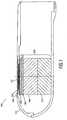
- FIG. 1is a cross-sectional schematic view of a transesophageal (TEE) ultrasonic probe 100.
- the ultrasonic probe 100includes a probe housing 110 that contains an ultrasonic transducer.
- the ultrasonic transducerincludes an acoustic sensor 120 commonly comprising a number of transducer array elements (to be described in further detail below).
- the transducer elementsmay be piezoelectric ceramic or micro-machined ultrasonic transducer (MUT) elements.
- An acoustic window 112, through which ultrasonic energy is both transmitted from and received by the ultrasonic probe 100,is located along a surface of the probe housing 110 and in front of the acoustic sensor 120.
- the acoustic sensor 120is joined to an integrated circuit (IC) 140. through an interface 130.
- the interface 130includes a redistribution layer 145 (shown and described in FIG. 2 ) applied over the active circuitry of the integrated circuit 140.
- the active circuitry of the IC 140can be formed on the surface of a suitable substrate (150 of FIG. 2 ) and is typically fabricated over a silicon (Si) substrate. However, other semiconductor substrate materials may be used to fabricate the IC 140.
- the IC substrateis bonded to a circuit board 155 having acoustic impedance that matches the acoustic impedance of the IC substrate.
- the circuit board 155is bonded to a backing material 160 by thin bonds to prevent acoustic reflections from the bonded surfaces.
- the acoustic sensor 120typically includes many hundreds or thousands of transducer elements, and preferably includes 2500 ultrasonic elements. Each of the elements requires an electrical connection to the electronic control circuitry (not shown) associated with the ultrasonic probe 100.
- the IC 140allows many such electrical connections to be combined, thereby reducing the number of individual connections within the ultrasonic probe 100.
- an acoustic backing 160is applied behind the circuit board 155 in order to absorb any ultrasonic energy that migrates through the circuit board 155.
- a heat sink 170is applied behind the acoustic backing 160 in order to remove heat from the acoustic sensor 120 and the IC 140.
- the acoustic sensor 120, interface 130, IC 140, circuit board 155, acoustic backing 160 and heat sink 170comprise an ultrasonic transducer 200.
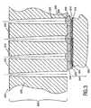
- FIG. 2is a cross-sectional schematic view illustrating a portion of the ultrasonic transducer 200 of FIG. 1 .
- a circuit board155 of FIG. 1
- an acoustic backing 160 and heat sink 170as shown in FIG. 1
- matching and dematching layersare omitted for clarity.
- the ultrasonic transducer 200includes an acoustic sensor 220 that, in this embodiment, comprises a plurality of piezoelectric ceramic transducer elements, an exemplar one of which is illustrated using reference numeral 210.
- a plurality of piezoelectric ceramic transducer elements 210are arranged in an array, which typically includes many hundreds or thousands of individual transducer elements, and in a preferred embodiment, includes 2500 elements.
- Each piezoelectric ceramic transducer element 210includes an element metalization layer 212a applied to the upper surface as shown.
- the element metalization layer 212aprovides an electrical ground connection for each element 210.
- the ground connectiontypically includes a conductor (not shown) connecting each element 210 to a suitable electrical ground.
- each piezoelectric ceramic transducer element 210is joined to the active circuitry 218 associated with IC 140 through a redistribution layer 145.
- the redistribution layer 145can be applied over the active circuitry 218, the IC pads, an exemplar one of which is illustrated using reference numeral 224, and the die passivation layer 214 located on the IC 140.
- the IC substrate 150 and the active circuitry 218comprise the IC 140.
- the die passivation layer 214is applied over the active circuitry 218 and the IC pads 224, leaving the IC pads 224 exposed.
- the redistribution layer 145includes a number of redistribution conductors, an exemplar one of which is shown using reference numeral 222, in contact with portions of the active circuitry 218 through the IC pads 224.
- the redistribution layer 145also includes a secondary passivation layer 216 applied over the redistribution conductors 222 and the die passivation layer 214.
- the redistribution conductors 222redistribute the connections of the active circuitry 218, through the IC pads 224, to appropriate locations corresponding to each piezoelectric ceramic transducer element 210.
- the redistribution conductor 222is a conductive material that connects each IC pad 224 to a respective metal contact 232, and can be formed using fine trace IC technology. Each metal contact 232 corresponds to a piezoelectric ceramic transducer element 210.
- the die passivation layer 214 and the secondary passivation layer 216can be formed of, for example, but not limited to, silicon dioxide or polymer.
- the redistribution layer 145aids in reducing capacitive coupling between the active circuitry 218 and the transducer elements 210.
- An additional passivation layer(not shown) can be applied between the die passivation layer 214 and the redistribution conductors 222 to further reduce capacitive coupling between the active circuitry 218 and the transducer elements 210, and is applicable to the other embodiments discussed.
- the secondary passivation layer 216aids in leveling the uneven surface resulting from the formation of the active circuitry 218 over the IC substrate 150.
- each piezoelectric ceramic transducer element 210is joined to a respective metal contact 232 using a conductive element 228.
- the conductive element 228can be, for example, a solder ball, or bump, that forms an electrical contact between the metal contact 232 and an element metalization layer 212b applied to the underside of each piezoelectric ceramic transducer element 210. In this manner, electrical contact between the piezoelectric ceramic transducer element 210 and the active circuitry 218 is achieved.
- solder bumpsas the conductive element 228, a variety of other techniques are available for electrically connecting the metal contact 232 to the element metalization layer 212b of each piezoelectric ceramic transducer element 210.
- solder bumpsinstead of solder bumps, gold bumps can be used.
- conductive adhesive or conductive polymer bumpscan be used to connect the metal contact 232 to the element metalization layer 212b.
- a technique known as "thin-line bonding"can be used to connect the element metalization layer 212b directly to the metal contact 232 resulting in a direct ohmic connection.
- the surface of the secondary passivation layer 216 and the metal contact 232can optionally be lapped flat, or planarized, to level the surface of the redistribution layer 145 and of the integrated circuit 140, prior to thin-line bonding the element metalization layer 212b to the metal contact 232.
- Adhesive material 226fills the gaps between each conductive element 228 and the space between each piezoelectric ceramic transducer element 210 and the secondary passivation layer 216.
- the adhesive 226is typically non-conductive and can be a variety of adhesives such as, for example but not limited to, epoxy.
- the adhesive 226can also function as a dematching material, which acts as an acoustic reflector.
- the ultrasonic transducer 200is typically constructed by forming the secondary passivation layer 216 and the metal contacts 232 over the active circuitry 218 of the IC 140.
- the conductive elements 228are then deposited over the metal contacts 232.
- the adhesive 226is then deposited and the material from which the transducer elements 210 are formed is bonded to the secondary passivation layer 216, resulting in an electrical connection between the element metalization layer 212b and the conductive elements 228.
- the transducer elements 210are then formed by removing a portion of the material that forms the transducer elements 210 and the element metalization layers 212a and 212b. For example, the transducer elements 210 can be cut using a dicing saw stopping before the saw contacts the metalization layer 212b.
- the remaining material of the transducer elements 210 and the metalization layer 212bcan then be removed by, for example, burning with a laser.
- the resulting saw kerf 215creates the independent transducer elements 210 and removes the electrical connection between transducer elements 210.
- FIG. 3is a cross-sectional schematic view of an alternative embodiment of the ultrasonic transducer 200 of FIG. 2 .
- the ultrasonic transducer 300 of FIG. 3includes an acoustic sensor 320 comprising a plurality of MUT elements 310.
- the MUT elements 310are formed on a MUT substrate 330.
- Each MUT element 310includes one or more MUT cells (not shown). If more than one MUT cell is used to form the MUT element 310, the MUT cells forming the MUT element typically are commonly connected.
- MUT elements 310can be fabricated on a substrate 330, such as silicon, using semiconductor device processing technology.
- Each MUT element 310includes an electrical ground connection (not shown) typically extending over the surface of each MUT element 310.
- the ground connectiontypically includes a conductor (not shown) connecting each MUT element 310 to a suitable electrical ground.
- each MUT element 310includes one or more small diameter holes, referred to as vias, an exemplar one of which is illustrated using reference numeral 325.
- the via 325extends through the MUT substrate 330 and makes contact with each MUT element 310.
- Each via 325is doped so as to be electrically conductive, thereby providing an electrical connection to each MUT element 310.
- each MUT element 310is located adjacent to a via 325.
- Each via 325extends through the MUT substrate 330 and contacts one of the conductive elements 328. In this manner, the conductive via 325 electrically couples the MUT element 310 to the conductive element 328.
- Each conductive element 328makes contact with a respective metal contact 332.
- Each metal contact 332makes electrical contact with a respective redistribution conductor 322, which in turn makes electrical contact with a respective IC pad 324.
- Each IC pad 324contacts a portion of the active circuitry 318.
- the active circuitry 318 located on the IC 340makes electrical contact, through the redistribution conductors 322, to the conductive elements 328 and to each MUT element 310.
- Adhesive material 326fills the gaps between each conductive element 328 and the space between the MUT substrate 330 and the secondary passivation layer 316.
- the adhesive 326is typically non-conductive and similar to the adhesive 226 described above.
- FIG. 4is a cross-sectional schematic view illustrating another alternative embodiment of the ultrasonic transducer 200 of FIG. 2 .
- the ultrasonic transducer 400 of FIG. 4includes acoustic sensor 420, which in this example includes a plurality of piezoelectric ceramic transducer elements, an exemplar one of which is illustrated using reference numeral 410.
- Each piezoelectric ceramic transducer element 410includes an element metalization layer 212a applied to the upper surface as shown.
- the element metalization layer 212aprovides an electrical ground connection for each element 410.
- the ground connectiontypically includes a conductor (not shown) connecting each element 410 to a suitable electrical ground.
- Each piezoelectric ceramic transducer element 410also includes an element metalization layer 412b applied to the underside as shown.
- the element metalization layer 412ballows direct electrical contact to be made between the piezoelectric ceramic transducer element 410 and the metal contact 432. As mentioned above, such a connection is typically referred to as a "thin-line bond.”
- the thin-line bonduses an adhesive polymer material to mechanically connect the metal contact 432 directly to the exposed surface of the element metalization layer 412b of the piezoelectric ceramic transducer element 410.
- the thin-line bondis achieved because of the microscopic surface roughness that exists on the exposed surface of the element metalization layer 412b and the metal contact 432. This microscopic surface roughness provides a direct ohmic connection between the metal contact 432 and the element metalization layer 412b.
- the metal contact 432is connected through the redistribution conductor 422 to the IC pad 424.
- the IC pad 424connects to the active circuitry 418 located on the IC 440.
- the redistribution layer 445includes the redistribution conductors 422 and a secondary passivation layer 416, which is similar to the secondary passivation layer 216, described above.
- the ultrasonic transducer 400is typically constructed by forming the secondary passivation layer 416 and the metal contacts 432 over the active circuitry 418 and IC pads 424 of the IC 440.
- the exposed surface of the secondary passivation layer 416 and portions of the metal contacts 432can then be lapped, or planarized, flat.
- the adhesive 426is then deposited and the material from which the transducer elements 410 are formed is bonded to the secondary passivation layer 416, resulting in a thin-line bond electrical connection between the element metalization layer 412b and the metal contacts 432.
- the transducer elements 410are then formed by removing a portion of the material that forms the transducer elements 410 and the element metalization layers 412a and 412b. As described above, the transducer elements 410 can be cut using a dicing saw stopping before the saw contacts the metalization layer 412b. The remaining material of the transducer elements 410 and the metalization layer 412b can then be removed using, for example, a laser. The resulting saw kerf 415 creates the independent transducer elements 410 and removes the electrical connection between transducer elements 410.
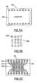
- FIG. 5Ais a plan view illustrating the IC 140 of FIG. 2 .
- the IC 140includes a plurality of IC pads, an exemplar one of which is illustrated using reference numeral 224.
- the IC pad 224connects to the active circuitry 218 and corresponds to the IC pad 224 of FIG. 2 .
- FIG. 5Bis a plan view illustrating a footprint of a two-dimensional (2D) acoustic sensor 500.
- the transducer array footprint 500illustrates 16 transducer elements, an exemplar one of which is illustrated using reference numeral 510, arranged in a 4x4 array.
- a typical transducer arrayincludes many hundreds or thousands of transducer elements.
- FIG. 5Cis a plan view illustrating the redistribution layer 145 of FIG. 2 including the transducer array footprint 510 of FIG. 5B shown using a dashed line.
- Each redistribution conductor 222connects one of the IC pads 224 to one of the pads 510 of the transducer array footprint 500.
- the redistribution conductors 222 in the redistribution layer 145make electrical connections between the IC pads 224 and each respective transducer array element 510. Accordingly, both the transducer array footprint 500 and the design of the active circuitry 218 can be independently optimized and each transducer array element 510 connected to the appropriate portion of the active circuitry 218.
- FIG. 6Ais a plan view illustrating an alternative embodiment of the IC of FIG. 5A .
- the IC 640includes a plurality of IC pads, an exemplar one of which is illustrated using reference numeral 624.
- the IC pad 624connects to the active circuitry 618.
- FIG. 6Bis a plan view illustrating a footprint of a one-dimensional (1D) acoustic sensor 605.
- the transducer array footprint 605includes a plurality of transducer elements, an exemplar one of which is illustrated using reference numeral 610, arranged in a 1 x 8 array.
- FIG. 6Cis a plan view illustrating an alternative embodiment of the redistribution layer 145 of FIG. 5A .
- the redistribution layer 645includes the transducer array footprint 605 of FIG. 6B .
- Each redistribution conductor 622connects one of the IC pads 624 to one of the pads 610 of the transducer array footprint 605.
- the dotted linesillustrate the outline of the transducer array footprint 605 shown in FIG. 6B .
- the redistribution conductors 622 in the redistribution layer 645make electrical connections between the IC pads 624 and each respective transducer array element 610. Accordingly, both the transducer array footprint 600 and the design of the active circuitry 618 can be independently optimized and each transducer array element 610 connected to the appropriate portion of the active circuitry 618.
- FIG. 7is a cross-sectional schematic view illustrating an alternative embodiment of the ultrasonic transducer 200 of FIG. 2 .
- the ultrasonic transducer 700includes an acoustic sensor 720, which comprises a plurality of piezoelectric ceramic transducer elements, an exemplar one of which is illustrated using reference numeral 710.
- Each piezoelectric ceramic transducer element 710includes an element metalization layer 712a applied to the upper surface as shown.
- the element metalization layer 712aprovides an electrical ground connection for each element 710.
- the ground connectiontypically includes a conductor (not shown) connecting each element 710 to a suitable electrical ground.
- Each piezoelectric ceramic transducer element 710also includes an element metalization layer 712b applied to the underside of each piezoelectric ceramic transducer element 710 as shown.
- each conductive element 728is a conductive polymer bump that is lapped flat, or planarized, as illustrated, and then metalized with a metalization layer 719.
- the adhesive layer 726is also planarized and metalized.
- Each conductive element 728is located over a respective metal contact 732.
- the element metalization layer 712b on the underside of each piezoelectric ceramic transducer element 710is thin-line bonded to the metalization layer 719 applied over each conductive element 728.
- the redistribution layer 745includes the redistribution conductors 722 and a secondary passivation layer 716, which is similar to the secondary passivation layer 216 described above.
- Each metal contact 732is connected through a respective redistribution conductor 722 to a respective IC pad 724.
- the IC pad 724connects to the active circuitry 718 located on the IC 740.
- the gap between the secondary passivation layer 716 and the exposed surface of the element metalization layer 712 on the piezoelectric ceramic transducer element 710is filled with a layer of adhesive 726.
- the adhesive 726is similar to the adhesive 226 described above.
- the transducer elements 710can be cut using a dicing saw stopping before the saw contacts the metalization layer 712b.
- the remaining material of the transducer elements 710 and the metalization layer 712bcan then be removed using, for example, a laser.
- the resulting saw kerf 715creates the independent transducer elements 710 and removes the electrical connection between transducer elements 710.
- FIG. 8Ais a cross-sectional schematic view illustrating one of the piezoelectric ceramic transducer elements of FIG. 2 .
- the piezoelectric ceramic transducer element 800includes a first matching layer 802 and a second matching layer 804 located over piezoelectric ceramic element 806.
- the matching layers 802 and 804are electrically conductive and generally include a metalization layer 811 applied over the matching layer 802.
- the matching layers 802 and 804help to match the acoustic impedance of the piezoelectric ceramic element 806 (approximately 30 megarayls (MRayls)) to the acoustic impedance of the patient (approximately 1.5 MRayls).
- the MRaylis a unit of measure of acoustic impedance.
- the 1.5 MRayl acoustic impedance of the patientcan be closely matched to the 30 MRayl acoustic impedance of the piezoelectric ceramic element 806.
- the acoustic impedance of the piezoelectric ceramic element 806can be altered by fabricating the element 806 using a composite piezoelectric ceramic material.
- a layer of an electrically conductive acoustic materialis bonded to the surface of the piezoelectric ceramic element 806 opposite that of the matching layer 804.
- the electrically conductive acoustic materialis a dematching layer 808 bonded to the piezoelectric ceramic element 806 as shown.
- the dematching layer 808acts as an acoustic reflector and may be a high impendance dematching layer, constructed of, for example, tungsten-carbide, having a cobalt or nickel blinder and having an acoustic impedance of approximately 80-100 MRayls.
- a low impedance dematching layerconstructed of, for example a polymer or polymer mixtures, such as, for example, epoxy having an acoustic impedance of approximately 3 MRayls and epoxy-metal mixtures such as epoxy-silver having an acoustic impedance of approximately 4.5 MRayls.
- the electrically conductive dematching layer 808might be tungsten-carbide, having acoustic impedance on the order of 80-100 MRayls. In this manner, the high impedance dematching layer 808 reflects acoustic energy back towards the piezoelectric ceramic element 806, which has an acoustic impedance of approximately 33 MRayls.
- the dematching layer 808is bonded to the IC 840, which has acoustic impedance on the order of 19 MRayls. Both surfaces of the dematching layer reflect waves, as known to those having ordinary skill in the art.
- the small amount of energy that passes through the dematching layer 808is transmitted into the IC substrate 850, circuit board 855 and into the backing 860 and absorbed. Both the circuit board 855 and the backing 860 match the acoustic impedance of the IC substrate 850.
- the IC 840is similar to the IC 140 described above and can be joined to the dematching layer 808 through interface 830, which is similar to interface 130 described above.
- the electrically conductive dematching layer 808might be a layer of epoxy-silver having acoustic impedance on the order of 4.5 MRayls.
- the low impedance dematching layer 808reflects acoustic energy back toward the piezoelectric ceramic element 806 that has an acoustic impedance of approximately 33 MRayls.
- the dematching layer 808is bonded to the IC 840, which has acoustic impedance on the order of 19 MRayls. Both surfaces of the dematching layer reflect waves as known to those skilled in the art.
- the small amount of energy that passes through the dematching layer 808is transmitted into the IC substrate 850, circuit board 855 and into the backing 860 and absorbed. Both the circuit board 855 and the backing 860 match the acoustic impedance of the IC substrate 850.
- additional dematching layerscan be added in alternating acoustic impedances to decrease the acoustic energy transmitted through the IC 840, circuit board 855 and into the backing 860.
- FIG. 8Bis a cross-sectional schematic view illustrating an alternative embodiment of the piezoelectric ceramic transducer element 800 of FIG. 8A .
- the transducer element 810includes one matching layer 812, over which is applied metalization layer 811.
- the matching layer 812is applied over the piezoelectric ceramic element 814, which has acoustic impedance of approximately 33 Mrayls.
- the acoustic impedance of the piezoelectric ceramic element 814is closely matched to the acoustic impedance of the IC substrate 850. This configuration may be desirable in some cases because it can provide a larger operating bandwidth.
- the transducer element 810could also be constructed using a composite polymer and piezoelectric ceramic element 814, which has acoustic impedance matched to the acoustic impedance of the IC substrate 850.
- Another configurationis to place the transducer element on a backing having conductors over the redistribution layer on the IC.
- a backing including conductorsis described in commonly assigned U.S. Patent No. 5,267,221 , entitled “BACKING FOR ACOUSTIC TRANSDUCER ARRAY” to Miller et al.
- the electrically conductive acoustic layer applied to the circuit board 855is a backing layer 816.
- the backing layer 816acts as an acoustic absorption material, thereby absorbing any acoustic energy that travels through the IC 840 and the circuit board 855.
- the dematching layer 808 of FIG. 8Amay be combined with the backing layer 816 of FIG. 8B to achieve the desired acoustic performance of the piezoelectric ceramic transducer element 800.
- FIG. 9is a cross-sectional schematic view illustrating another alternative embodiment 900 of the ultrasonic transducer 200 of FIG. 2 .
- the ultrasonic transducer 900includes an acoustic sensor 920 that, in this embodiment, comprises a plurality of piezoelectric ceramic transducer elements, an exemplar one of which is illustrated using reference numeral 910.
- a plurality of piezoelectric ceramic transducer elements 910are arranged in an array, which typically includes many hundreds or thousands of individual transducer elements, and in a preferred embodiment, includes 2500 elements.
- Each piezoelectric ceramic transducer element 910includes an element metalization layer 912a applied to the upper surface as shown.
- the element metalization layer 912aprovides an electrical ground connection for each element 910.
- the ground connectiontypically includes a conductor (not shown) connecting each element 910 to a suitable electrical ground.
- each piezoelectric ceramic transducer element 910is joined to the active circuitry 918 associated with IC 940 through a die passivation layer 914 in which the metal contacts 932 are connected directly to the IC pads 924, thereby eliminating the redistribution conductors referred to above.
- the die passivation layer 914can be applied over the active circuitry 918 and IC pads, an exemplar one of which is illustrated using reference numeral 924.
- the die passivation later 914can be formed using, for example, silicon dioxide or polymer.
- Each IC pad 924is in electrical contact with a corresponding portion of the active circuitry 918 and the underside of metal contact 932. As illustrated in FIG. 9 , the redistribution conductors and the secondary passivation layer referred to above are omitted because the transducer elements 910 are each aligned over corresponding IC pads 924.
- each piezoelectric ceramic transducer element 910is joined to a respective metal contact 932 using a conductive element 928.
- the conductive element 928can be, for example, a solder bump that forms an electrical contact between the metal contact 932 and an element metalization layer 912b applied to the underside of each piezoelectric ceramic transducer element 910. In this manner, electrical contact between the piezoelectric ceramic transducer element 910 and the active circuitry 918 is achieved.
- solder bumpsas the conductive element 928, the variety of other techniques mentioned above with respect to FIG. 2 are available for electrically connecting the metal contact 932 to the element metalization layer 912b of each piezoelectric ceramic transducer element 910.
- Adhesive material 926fills the gaps between each conductive element 928 and the space between each piezoelectric ceramic transducer element 910 and the die passivation layer 914.
- the adhesive 926is typically non-conductive and can be a variety of adhesives such as, for example but not limited to, epoxy.
- the ultrasonic transducer 900is typically constructed by forming the die passivation layer 914 and the metal contacts 932 over the active circuitry 918 of the IC 940.
- the conductive elements 928are then deposited over the metal contacts 932.
- the adhesive 926is then deposited and the material from which the transducer elements 910 are formed is bonded to the die passivation layer 914, resulting in an electrical connection between the element metalization layer 912b and the conductive elements 928.
- the transducer elements 910are then formed by removing a portion of the material that forms the transducer elements 910 and the element metalization layers 912a and 912b by, for example, cutting and lasing as described above.
- FIG. 10is a cross-sectional schematic view illustrating an alternative embodiment 1000 of the ultrasonic transducer 400 of FIG. 4 .
- the ultrasonic transducer 1000 of FIG. 10includes acoustic sensor 1020, which in this example includes a plurality of piezoelectric ceramic transducer elements, an exemplar one of which is illustrated using reference numeral 1010.
- Each piezoelectric cerainic transducer element 1010includes an element metalization layer 1012a applied to the upper surface as shown.
- the element metalization layer 1012aprovides an electrical ground connection for each element 1010.
- the ground connectiontypically includes a conductor (not shown) connecting each element 1010 to a suitable electrical ground.
- Each piezoelectric ceramic transducer element 1010also includes an element metalization layer 1012b applied to the underside as shown.
- the element metalization layer 1012ballows direct electrical contact to be made between the piezoelectric ceramic transducer element 1010 and the metal contact 1032. As mentioned above, such a connection is typically referred to as a "thin-line bond.”
- the thin-line bondelectrically connects the metal contact 1032 directly to the exposed surface of the element metalization layer 1012b of the piezoelectric ceramic transducer element 1010, typically using an adhesive polymer.
- the thin-line bondis achieved because of the microscopic surface roughness that exists on the exposed surface of the element metalization layer 1012b and the metal contact 1032. This microscopic surface roughness provides a direct ohmic connection between the metal contact 1032 and the element metalization layer 1012b.
- the metal contact 1032connects directly to the IC bond pad 1024 without the use of the redistribution conductor described above.
- the IC pad 1024connects to the active circuitry 1018 located on the IC 1040.
- the surface of the secondary passivation layer 1016 and a portion of the metal contact 1032is lapped, or planarized, and metalized to level the surface of the IC 1040 and to provide an even surface over which to attach the transducer elements 1010.
- the ultrasonic transducer 1000is typically constructed by forming the IC bond pads 1024 directly over portions of the active circuitry 1018.
- the metal contacts 1032are then formed over the IC bond pads 1024, and the die passivation layer 1014 and the secondary passivation layer 1016 are then formed over the active circuitry 1018 and the IC pads 1024 of the IC 1040.
- the exposed surface of the secondary passivation layer 1016 and portions of the metal contacts 1032are then lapped, or planarized, flat and metalized.
- the element metalization layer 1012bis then thin-line bonded to the planarized surface of the secondary passivation layer 1016, resulting in a thin-line bond electrical connection between the element metalization layer 1012b and the metal contacts 1032.
- the transducer elements 1010are then formed by removing a portion of the material that forms the transducer elements 1010 and the element metalization layers 1012a and 1012b by, for example, cutting and lasing as described above.
Landscapes
- Health & Medical Sciences (AREA)
- Engineering & Computer Science (AREA)
- Life Sciences & Earth Sciences (AREA)
- Physics & Mathematics (AREA)
- Remote Sensing (AREA)
- Radar, Positioning & Navigation (AREA)
- Nuclear Medicine, Radiotherapy & Molecular Imaging (AREA)
- Public Health (AREA)
- Pathology (AREA)
- Radiology & Medical Imaging (AREA)
- Biomedical Technology (AREA)
- Heart & Thoracic Surgery (AREA)
- Medical Informatics (AREA)
- Molecular Biology (AREA)
- Surgery (AREA)
- Animal Behavior & Ethology (AREA)
- General Health & Medical Sciences (AREA)
- Biophysics (AREA)
- Veterinary Medicine (AREA)
- Mechanical Engineering (AREA)
- Gynecology & Obstetrics (AREA)
- Acoustics & Sound (AREA)
- Computer Networks & Wireless Communication (AREA)
- General Physics & Mathematics (AREA)
- Transducers For Ultrasonic Waves (AREA)
- Ultra Sonic Daignosis Equipment (AREA)
- Investigating Or Analyzing Materials By The Use Of Ultrasonic Waves (AREA)
- Apparatuses For Generation Of Mechanical Vibrations (AREA)
Description
- The present invention relates generally to ultrasonic transducers, and, more particularly, to a system for attaching the acoustic element of an ultrasonic transducer to an integrated circuit.
- Ultrasonic transducers have been available for quite some time and are particularly useful for non-invasive medical diagnostic imaging. Ultrasonic transducers are typically formed of either piezoelectric elements or micro-machined ultrasonic transducer (MUT) elements. The piezoelectric elements typically are made of a piezoelectric ceramic such as lead zirconate titanate (commonly referred to as PZT), with a plurality of elements being -arranged to form a transducer assembly. A MUT is formed using known semiconductor manufacturing techniques resulting in a capacitive ultrasonic transducer cell that comprises, in essence, a flexible membrane supported around its edges over a silicon substrate. By applying contact material, in the form of electrodes, to the membrane, or a portion of the membrane, and to the base of the cavity in the silicon substrate, and then by applying appropriate voltage signals to the electrodes, the MUT may be energized such that an appropriate ultrasonic wave is produced. Similarly, when electrically biased, the membrane of the MUT may be used to receive ultrasonic signals by capturing reflected ultrasonic energy and transforming that energy into movement of the electrically biased membrane, which then generates a receive signal.
- The transducer elements can be combined with control circuitry forming a transducer assembly, which is then further assembled into a housing possibly including additional control electronics, in the form of electronic circuit boards, the combination of which forms an ultrasonic probe. This ultrasonic probe, which may include various acoustic matching layers, backing layers, and dematching layers, may then be used to send and receive ultrasonic signals through body tissue.
- In the past, joining an acoustic sensor, such as a piezoelectric ceramic transducer element or a MUT element, to the electrical control circuitry required the use of many individual wires to connect each element of the transducer array to the control circuitry. In the case of large transducer arrays having many hundreds or thousands of elements, large wiring harnesses were required. Unfortunately, a large wiring harness increases the bulk and cost of the ultrasonic probe. For ultrasonic probes designed to be used inside the human body, it is desirable to reduce the overall size of the ultrasonic probe and cable. One manner of reducing the size of the probe is to provide the transducer element control electronics on an integrated circuit (IC) assembly. An IC in proximity to the transducer array may be used to transmit and receive from many small transducer elements and may also be used to combine the signals, thereby reducing or eliminating the bulky and expensive cables that typically connect the ultrasonic probe elements to the control electronics.
- Placing the transducer array over the IC results in greater packaging efficiency. Unfortunately, there is no convenient way to connect the piezoelectric ceramic or MUT transducer elements to the control electronics.
US5744898 , "Ultrasound transducer array with transmitter/receiver integrated circuitry", for instance, discloses a transducer array where piezoelectric ceramic transducer elements are connected to the control electronics via a distribution layer, consisting of multiple layers of connectors that connect to each other through vias.- Therefore, it would be desirable to have a way in which to connect both the piezoelectric ceramic and MUT elements of an ultrasonic transducer array directly to an IC.
- The invention is a system according to
claim 1 and a method according to claim 15 for attaching an acoustic element to an integrated circuit (IC). The system provides various ways to connect piezoelectric ceramic or MUT transducer elements to an IC, thus reducing the number of conductors required to connect each element of the transducer array to the IC by combining the signals in the IC. In another aspect of the invention, the transducer elements include an electrically conductive acoustic layer having a backing layer and/or a dematching layer that is connected to an IC. - Other systems, methods, features, and advantages of the invention will be or will become apparent to one with skill in the art upon examination of the following drawings and detailed description. It is intended that all such additional systems, methods, features, and advantages be included within this description, be within the scope of the present invention, and be protected by the accompanying claims.
- The present invention, as defined in the claims, can be better understood with reference to the following drawings. The components within the drawings are not necessarily to scale relative to each other, emphasis instead being placed upon clearly illustrating the principles of the present invention.
FIG. 1 is a cross-sectional schematic view of a transesophageal (TEE) ultrasonic probe.FIG. 2 is a cross-sectional schematic view illustrating a portion of the ultrasonic transducer ofFIG. 1 .FIG. 3 is a cross-sectional schematic view of an alternative embodiment of the ultrasonic transducer ofFIG. 2 .FIG. 4 is a cross-sectional schematic view illustrating another alternative embodiment of the ultrasonic transducer ofFIG. 2 .FIG. 5A is a plan view illustrating the IC in the ultrasonic transducer ofFIG. 2 .FIG. 5B is a plan view illustrating a footprint of a two-dimensional (2D) acoustic sensor.FIG. 5C is a plan view illustrating the redistribution layer ofFIG. 2 including the transducer array footprint ofFIG. 5B .FIG. 6A is a plan view illustrating an alternative embodiment of the IC ofFIG. 5A .FIG. 6B is a plan view illustrating a footprint of a one-dimensional (1D) acoustic sensor.FIG. 6C is a plan view illustrating a redistribution layer including the transducer array footprint ofFIG. 6B .FIG. 7 is a cross-sectional schematic view illustrating an alternative embodiment of the ultrasonic transducer ofFIG. 2 .FIG. 8A is a cross-sectional schematic view illustrating one of the piezoelectric ceramic transducer elements ofFIG. 2 .FIG. 8B is a cross-sectional schematic view illustrating an alternative embodiment of the piezoelectric ceramic transducer element ofFIG. 8A .FIG. 9 is a cross-sectional schematic view illustrating another alternative embodiment of the ultrasonic transducer ofFIG. 2 .FIG. 10 is a cross-sectional schematic view illustrating an alternative embodiment of the ultrasonic transducer ofFIG. 4 .- The invention to be described hereafter is applicable to piezoelectric ceramic and micro-machined ultrasonic transducer (MUT) elements connected to an integrated circuit (IC).
FIG. 1 is a cross-sectional schematic view of a transesophageal (TEE)ultrasonic probe 100. Theultrasonic probe 100 includes aprobe housing 110 that contains an ultrasonic transducer. The ultrasonic transducer includes anacoustic sensor 120 commonly comprising a number of transducer array elements (to be described in further detail below). The transducer elements may be piezoelectric ceramic or micro-machined ultrasonic transducer (MUT) elements. Anacoustic window 112, through which ultrasonic energy is both transmitted from and received by theultrasonic probe 100, is located along a surface of theprobe housing 110 and in front of theacoustic sensor 120.- The
acoustic sensor 120 is joined to an integrated circuit (IC) 140. through aninterface 130. Theinterface 130 includes a redistribution layer 145 (shown and described inFIG. 2 ) applied over the active circuitry of theintegrated circuit 140. The active circuitry of theIC 140 can be formed on the surface of a suitable substrate (150 ofFIG. 2 ) and is typically fabricated over a silicon (Si) substrate. However, other semiconductor substrate materials may be used to fabricate theIC 140. The IC substrate is bonded to acircuit board 155 having acoustic impedance that matches the acoustic impedance of the IC substrate. Thecircuit board 155 is bonded to abacking material 160 by thin bonds to prevent acoustic reflections from the bonded surfaces. - The
acoustic sensor 120 typically includes many hundreds or thousands of transducer elements, and preferably includes 2500 ultrasonic elements. Each of the elements requires an electrical connection to the electronic control circuitry (not shown) associated with theultrasonic probe 100. TheIC 140 allows many such electrical connections to be combined, thereby reducing the number of individual connections within theultrasonic probe 100. - Typically, an
acoustic backing 160 is applied behind thecircuit board 155 in order to absorb any ultrasonic energy that migrates through thecircuit board 155. Aheat sink 170 is applied behind theacoustic backing 160 in order to remove heat from theacoustic sensor 120 and theIC 140. Theacoustic sensor 120,interface 130,IC 140,circuit board 155,acoustic backing 160 andheat sink 170 comprise anultrasonic transducer 200. FIG. 2 is a cross-sectional schematic view illustrating a portion of theultrasonic transducer 200 ofFIG. 1 . Although omitted from theultrasonic transducer 200 ofFIG. 2 , there is commonly a circuit board (155 ofFIG. 1 ), anacoustic backing 160 and heat sink 170 (as shown inFIG. 1 ) associated with theultrasonic transducer 200. Furthermore, matching and dematching layers are omitted for clarity.- The
ultrasonic transducer 200 includes anacoustic sensor 220 that, in this embodiment, comprises a plurality of piezoelectric ceramic transducer elements, an exemplar one of which is illustrated usingreference numeral 210. A plurality of piezoelectricceramic transducer elements 210 are arranged in an array, which typically includes many hundreds or thousands of individual transducer elements, and in a preferred embodiment, includes 2500 elements. Each piezoelectricceramic transducer element 210 includes anelement metalization layer 212a applied to the upper surface as shown. Theelement metalization layer 212a provides an electrical ground connection for eachelement 210. The ground connection typically includes a conductor (not shown) connecting eachelement 210 to a suitable electrical ground. In accordance with an aspect of the invention, each piezoelectricceramic transducer element 210 is joined to theactive circuitry 218 associated withIC 140 through aredistribution layer 145. Theredistribution layer 145 can be applied over theactive circuitry 218, the IC pads, an exemplar one of which is illustrated usingreference numeral 224, and thedie passivation layer 214 located on theIC 140. TheIC substrate 150 and theactive circuitry 218 comprise theIC 140. Thedie passivation layer 214 is applied over theactive circuitry 218 and theIC pads 224, leaving theIC pads 224 exposed. - The
redistribution layer 145 includes a number of redistribution conductors, an exemplar one of which is shown usingreference numeral 222, in contact with portions of theactive circuitry 218 through theIC pads 224. Theredistribution layer 145 also includes asecondary passivation layer 216 applied over theredistribution conductors 222 and thedie passivation layer 214. Theredistribution conductors 222 redistribute the connections of theactive circuitry 218, through theIC pads 224, to appropriate locations corresponding to each piezoelectricceramic transducer element 210. Theredistribution conductor 222 is a conductive material that connects eachIC pad 224 to arespective metal contact 232, and can be formed using fine trace IC technology. Eachmetal contact 232 corresponds to a piezoelectricceramic transducer element 210. - The
die passivation layer 214 and thesecondary passivation layer 216 can be formed of, for example, but not limited to, silicon dioxide or polymer. Theredistribution layer 145 aids in reducing capacitive coupling between theactive circuitry 218 and thetransducer elements 210. An additional passivation layer (not shown) can be applied between thedie passivation layer 214 and theredistribution conductors 222 to further reduce capacitive coupling between theactive circuitry 218 and thetransducer elements 210, and is applicable to the other embodiments discussed. Furthermore, thesecondary passivation layer 216 aids in leveling the uneven surface resulting from the formation of theactive circuitry 218 over theIC substrate 150. - In one embodiment, each piezoelectric
ceramic transducer element 210 is joined to arespective metal contact 232 using aconductive element 228. Theconductive element 228 can be, for example, a solder ball, or bump, that forms an electrical contact between themetal contact 232 and anelement metalization layer 212b applied to the underside of each piezoelectricceramic transducer element 210. In this manner, electrical contact between the piezoelectricceramic transducer element 210 and theactive circuitry 218 is achieved. Although illustrated inFIG. 2 using solder bumps as theconductive element 228, a variety of other techniques are available for electrically connecting themetal contact 232 to theelement metalization layer 212b of each piezoelectricceramic transducer element 210. For example, instead of solder bumps, gold bumps can be used. Further, conductive adhesive or conductive polymer bumps can be used to connect themetal contact 232 to theelement metalization layer 212b. Further still, as will be described below with respect toFIG. 4 , a technique known as "thin-line bonding" can be used to connect theelement metalization layer 212b directly to themetal contact 232 resulting in a direct ohmic connection. In such an embodiment, the surface of thesecondary passivation layer 216 and themetal contact 232 can optionally be lapped flat, or planarized, to level the surface of theredistribution layer 145 and of theintegrated circuit 140, prior to thin-line bonding theelement metalization layer 212b to themetal contact 232. Adhesive material 226 fills the gaps between eachconductive element 228 and the space between each piezoelectricceramic transducer element 210 and thesecondary passivation layer 216. The adhesive 226 is typically non-conductive and can be a variety of adhesives such as, for example but not limited to, epoxy. The adhesive 226 can also function as a dematching material, which acts as an acoustic reflector.- The
ultrasonic transducer 200 is typically constructed by forming thesecondary passivation layer 216 and themetal contacts 232 over theactive circuitry 218 of theIC 140. Theconductive elements 228 are then deposited over themetal contacts 232. The adhesive 226 is then deposited and the material from which thetransducer elements 210 are formed is bonded to thesecondary passivation layer 216, resulting in an electrical connection between theelement metalization layer 212b and theconductive elements 228. Thetransducer elements 210 are then formed by removing a portion of the material that forms thetransducer elements 210 and theelement metalization layers transducer elements 210 can be cut using a dicing saw stopping before the saw contacts themetalization layer 212b. The remaining material of thetransducer elements 210 and themetalization layer 212b can then be removed by, for example, burning with a laser. The resultingsaw kerf 215 creates theindependent transducer elements 210 and removes the electrical connection betweentransducer elements 210. FIG. 3 is a cross-sectional schematic view of an alternative embodiment of theultrasonic transducer 200 ofFIG. 2 . Theultrasonic transducer 300 ofFIG. 3 includes anacoustic sensor 320 comprising a plurality ofMUT elements 310. TheMUT elements 310 are formed on aMUT substrate 330. EachMUT element 310 includes one or more MUT cells (not shown). If more than one MUT cell is used to form theMUT element 310, the MUT cells forming the MUT element typically are commonly connected. As known to those having ordinary skill in the art,MUT elements 310 can be fabricated on asubstrate 330, such as silicon, using semiconductor device processing technology. EachMUT element 310 includes an electrical ground connection (not shown) typically extending over the surface of eachMUT element 310. The ground connection typically includes a conductor (not shown) connecting eachMUT element 310 to a suitable electrical ground.- In accordance with an aspect of the invention, each
MUT element 310 includes one or more small diameter holes, referred to as vias, an exemplar one of which is illustrated usingreference numeral 325. The via 325 extends through theMUT substrate 330 and makes contact with eachMUT element 310. Each via 325 is doped so as to be electrically conductive, thereby providing an electrical connection to eachMUT element 310. In accordance with this aspect of the invention, eachMUT element 310 is located adjacent to a via 325. Each via 325 extends through theMUT substrate 330 and contacts one of theconductive elements 328. In this manner, the conductive via 325 electrically couples theMUT element 310 to theconductive element 328. It should be noted that all the alternative conductive elements mentioned above inFIG. 2 apply toFIG. 3 . Eachconductive element 328 makes contact with arespective metal contact 332. Eachmetal contact 332 makes electrical contact with arespective redistribution conductor 322, which in turn makes electrical contact with arespective IC pad 324. EachIC pad 324 contacts a portion of theactive circuitry 318. In this manner, theactive circuitry 318 located on theIC 340 makes electrical contact, through theredistribution conductors 322, to theconductive elements 328 and to eachMUT element 310.Adhesive material 326 fills the gaps between eachconductive element 328 and the space between theMUT substrate 330 and the secondary passivation layer 316. The adhesive 326 is typically non-conductive and similar to the adhesive 226 described above. FIG. 4 is a cross-sectional schematic view illustrating another alternative embodiment of theultrasonic transducer 200 ofFIG. 2 . Theultrasonic transducer 400 ofFIG. 4 includesacoustic sensor 420, which in this example includes a plurality of piezoelectric ceramic transducer elements, an exemplar one of which is illustrated usingreference numeral 410. Each piezoelectricceramic transducer element 410 includes anelement metalization layer 212a applied to the upper surface as shown. Theelement metalization layer 212a provides an electrical ground connection for eachelement 410. The ground connection typically includes a conductor (not shown) connecting eachelement 410 to a suitable electrical ground. Each piezoelectricceramic transducer element 410 also includes anelement metalization layer 412b applied to the underside as shown. Theelement metalization layer 412b allows direct electrical contact to be made between the piezoelectricceramic transducer element 410 and themetal contact 432. As mentioned above, such a connection is typically referred to as a "thin-line bond." The thin-line bond uses an adhesive polymer material to mechanically connect themetal contact 432 directly to the exposed surface of theelement metalization layer 412b of the piezoelectricceramic transducer element 410. The thin-line bond is achieved because of the microscopic surface roughness that exists on the exposed surface of theelement metalization layer 412b and themetal contact 432. This microscopic surface roughness provides a direct ohmic connection between themetal contact 432 and theelement metalization layer 412b. Themetal contact 432 is connected through theredistribution conductor 422 to theIC pad 424. TheIC pad 424 connects to theactive circuitry 418 located on theIC 440. Theredistribution layer 445 includes theredistribution conductors 422 and asecondary passivation layer 416, which is similar to thesecondary passivation layer 216, described above.- Similar to the
ultrasonic transducer 200 ofFIG. 2 , theultrasonic transducer 400 is typically constructed by forming thesecondary passivation layer 416 and themetal contacts 432 over theactive circuitry 418 andIC pads 424 of theIC 440. The exposed surface of thesecondary passivation layer 416 and portions of themetal contacts 432 can then be lapped, or planarized, flat. - The adhesive 426 is then deposited and the material from which the
transducer elements 410 are formed is bonded to thesecondary passivation layer 416, resulting in a thin-line bond electrical connection between theelement metalization layer 412b and themetal contacts 432. Thetransducer elements 410 are then formed by removing a portion of the material that forms thetransducer elements 410 and theelement metalization layers transducer elements 410 can be cut using a dicing saw stopping before the saw contacts themetalization layer 412b. The remaining material of thetransducer elements 410 and themetalization layer 412b can then be removed using, for example, a laser. The resultingsaw kerf 415 creates theindependent transducer elements 410 and removes the electrical connection betweentransducer elements 410. FIG. 5A is a plan view illustrating theIC 140 ofFIG. 2 . TheIC 140 includes a plurality of IC pads, an exemplar one of which is illustrated usingreference numeral 224. TheIC pad 224 connects to theactive circuitry 218 and corresponds to theIC pad 224 ofFIG. 2 .FIG. 5B is a plan view illustrating a footprint of a two-dimensional (2D)acoustic sensor 500. For simplicity, thetransducer array footprint 500 illustrates 16 transducer elements, an exemplar one of which is illustrated usingreference numeral 510, arranged in a 4x4 array. However, a typical transducer array includes many hundreds or thousands of transducer elements.FIG. 5C is a plan view illustrating theredistribution layer 145 ofFIG. 2 including thetransducer array footprint 510 ofFIG. 5B shown using a dashed line. Eachredistribution conductor 222 connects one of theIC pads 224 to one of thepads 510 of thetransducer array footprint 500. Theredistribution conductors 222 in theredistribution layer 145 make electrical connections between theIC pads 224 and each respectivetransducer array element 510. Accordingly, both thetransducer array footprint 500 and the design of theactive circuitry 218 can be independently optimized and eachtransducer array element 510 connected to the appropriate portion of theactive circuitry 218.FIG. 6A is a plan view illustrating an alternative embodiment of the IC ofFIG. 5A . TheIC 640 includes a plurality of IC pads, an exemplar one of which is illustrated usingreference numeral 624. TheIC pad 624 connects to theactive circuitry 618.FIG. 6B is a plan view illustrating a footprint of a one-dimensional (1D)acoustic sensor 605. Thetransducer array footprint 605 includes a plurality of transducer elements, an exemplar one of which is illustrated usingreference numeral 610, arranged in a 1 x 8 array.FIG. 6C is a plan view illustrating an alternative embodiment of theredistribution layer 145 ofFIG. 5A . Theredistribution layer 645 includes thetransducer array footprint 605 ofFIG. 6B . Eachredistribution conductor 622 connects one of theIC pads 624 to one of thepads 610 of thetransducer array footprint 605. Further, inFIG. 6C , the dotted lines illustrate the outline of thetransducer array footprint 605 shown inFIG. 6B . In this manner, theredistribution conductors 622 in theredistribution layer 645 make electrical connections between theIC pads 624 and each respectivetransducer array element 610. Accordingly, both the transducer array footprint 600 and the design of theactive circuitry 618 can be independently optimized and eachtransducer array element 610 connected to the appropriate portion of theactive circuitry 618.FIG. 7 is a cross-sectional schematic view illustrating an alternative embodiment of theultrasonic transducer 200 ofFIG. 2 . Theultrasonic transducer 700 includes anacoustic sensor 720, which comprises a plurality of piezoelectric ceramic transducer elements, an exemplar one of which is illustrated usingreference numeral 710. Each piezoelectricceramic transducer element 710 includes anelement metalization layer 712a applied to the upper surface as shown. Theelement metalization layer 712a provides an electrical ground connection for eachelement 710. The ground connection typically includes a conductor (not shown) connecting eachelement 710 to a suitable electrical ground. Each piezoelectricceramic transducer element 710 also includes anelement metalization layer 712b applied to the underside of each piezoelectricceramic transducer element 710 as shown. In the embodiment shown inFIG. 7 , eachconductive element 728 is a conductive polymer bump that is lapped flat, or planarized, as illustrated, and then metalized with ametalization layer 719. Theadhesive layer 726 is also planarized and metalized. Eachconductive element 728 is located over arespective metal contact 732. Theelement metalization layer 712b on the underside of each piezoelectricceramic transducer element 710 is thin-line bonded to themetalization layer 719 applied over eachconductive element 728.- The
redistribution layer 745 includes theredistribution conductors 722 and asecondary passivation layer 716, which is similar to thesecondary passivation layer 216 described above. - Each
metal contact 732 is connected through arespective redistribution conductor 722 to arespective IC pad 724. TheIC pad 724 connects to theactive circuitry 718 located on theIC 740. The gap between thesecondary passivation layer 716 and the exposed surface of the element metalization layer 712 on the piezoelectricceramic transducer element 710 is filled with a layer ofadhesive 726. The adhesive 726 is similar to the adhesive 226 described above. As described above, thetransducer elements 710 can be cut using a dicing saw stopping before the saw contacts themetalization layer 712b. The remaining material of thetransducer elements 710 and themetalization layer 712b can then be removed using, for example, a laser. The resultingsaw kerf 715 creates theindependent transducer elements 710 and removes the electrical connection betweentransducer elements 710. FIG. 8A is a cross-sectional schematic view illustrating one of the piezoelectric ceramic transducer elements ofFIG. 2 . The piezoelectricceramic transducer element 800 includes afirst matching layer 802 and asecond matching layer 804 located over piezoelectricceramic element 806. The matching layers 802 and 804 are electrically conductive and generally include ametalization layer 811 applied over thematching layer 802. The matching layers 802 and 804 help to match the acoustic impedance of the piezoelectric ceramic element 806 (approximately 30 megarayls (MRayls)) to the acoustic impedance of the patient (approximately 1.5 MRayls). The MRayl is a unit of measure of acoustic impedance.- For example, by using the matching layers 802 and 804, in a ¼ wave arrangement, the 1.5 MRayl acoustic impedance of the patient can be closely matched to the 30 MRayl acoustic impedance of the piezoelectric
ceramic element 806. Alternatively, instead of using a pure piezoelectric ceramic element, the acoustic impedance of the piezoelectricceramic element 806 can be altered by fabricating theelement 806 using a composite piezoelectric ceramic material. - In accordance with another aspect of the invention, a layer of an electrically conductive acoustic material is bonded to the surface of the piezoelectric
ceramic element 806 opposite that of thematching layer 804. In one embodiment, the electrically conductive acoustic material is adematching layer 808 bonded to the piezoelectricceramic element 806 as shown. Thedematching layer 808 acts as an acoustic reflector and may be a high impendance dematching layer, constructed of, for example, tungsten-carbide, having a cobalt or nickel blinder and having an acoustic impedance of approximately 80-100 MRayls. Alternatively, a low impedance dematching layer, constructed of, for example a polymer or polymer mixtures, such as, for example, epoxy having an acoustic impedance of approximately 3 MRayls and epoxy-metal mixtures such as epoxy-silver having an acoustic impedance of approximately 4.5 MRayls. For example, the electricallyconductive dematching layer 808 might be tungsten-carbide, having acoustic impedance on the order of 80-100 MRayls. In this manner, the highimpedance dematching layer 808 reflects acoustic energy back towards the piezoelectricceramic element 806, which has an acoustic impedance of approximately 33 MRayls. Thedematching layer 808 is bonded to theIC 840, which has acoustic impedance on the order of 19 MRayls. Both surfaces of the dematching layer reflect waves, as known to those having ordinary skill in the art. The small amount of energy that passes through thedematching layer 808 is transmitted into theIC substrate 850,circuit board 855 and into thebacking 860 and absorbed. Both thecircuit board 855 and thebacking 860 match the acoustic impedance of theIC substrate 850. - As known to those having ordinary skill in the art, other than the
interface 830, which is similar to theinterface 130 described above, all elements inFIG. 8A are attached using acoustic bonds. TheIC 840 is similar to theIC 140 described above and can be joined to thedematching layer 808 throughinterface 830, which is similar tointerface 130 described above. - Alternatively, the electrically
conductive dematching layer 808 might be a layer of epoxy-silver having acoustic impedance on the order of 4.5 MRayls. In this embodiment, the lowimpedance dematching layer 808 reflects acoustic energy back toward the piezoelectricceramic element 806 that has an acoustic impedance of approximately 33 MRayls. Thedematching layer 808 is bonded to theIC 840, which has acoustic impedance on the order of 19 MRayls. Both surfaces of the dematching layer reflect waves as known to those skilled in the art. The small amount of energy that passes through thedematching layer 808 is transmitted into theIC substrate 850,circuit board 855 and into thebacking 860 and absorbed. Both thecircuit board 855 and thebacking 860 match the acoustic impedance of theIC substrate 850. As known to those having ordinary skill in the art, additional dematching layers can be added in alternating acoustic impedances to decrease the acoustic energy transmitted through theIC 840,circuit board 855 and into thebacking 860. FIG. 8B is a cross-sectional schematic view illustrating an alternative embodiment of the piezoelectricceramic transducer element 800 ofFIG. 8A . Thetransducer element 810 includes onematching layer 812, over which is appliedmetalization layer 811. Thematching layer 812 is applied over the piezoelectricceramic element 814, which has acoustic impedance of approximately 33 Mrayls. The acoustic impedance of the piezoelectricceramic element 814 is closely matched to the acoustic impedance of theIC substrate 850. This configuration may be desirable in some cases because it can provide a larger operating bandwidth. Thetransducer element 810 could also be constructed using a composite polymer and piezoelectricceramic element 814, which has acoustic impedance matched to the acoustic impedance of theIC substrate 850.- Another configuration is to place the transducer element on a backing having conductors over the redistribution layer on the IC. Such a backing including conductors is described in commonly assigned
U.S. Patent No. 5,267,221 , entitled "BACKING FOR ACOUSTIC TRANSDUCER ARRAY" to Milleret al. - As known to those having ordinary skill in the art, other than the
interface 830, which is similar to theinterface 130 described above, all elements inFIG. 8B are attached using acoustic bonds. - In this embodiment, the electrically conductive acoustic layer applied to the
circuit board 855 is abacking layer 816. Thebacking layer 816 acts as an acoustic absorption material, thereby absorbing any acoustic energy that travels through theIC 840 and thecircuit board 855. Furthermore, thedematching layer 808 ofFIG. 8A may be combined with thebacking layer 816 ofFIG. 8B to achieve the desired acoustic performance of the piezoelectricceramic transducer element 800. FIG. 9 is a cross-sectional schematic view illustrating anotheralternative embodiment 900 of theultrasonic transducer 200 ofFIG. 2 . Theultrasonic transducer 900 includes anacoustic sensor 920 that, in this embodiment, comprises a plurality of piezoelectric ceramic transducer elements, an exemplar one of which is illustrated usingreference numeral 910. A plurality of piezoelectricceramic transducer elements 910 are arranged in an array, which typically includes many hundreds or thousands of individual transducer elements, and in a preferred embodiment, includes 2500 elements. Each piezoelectricceramic transducer element 910 includes anelement metalization layer 912a applied to the upper surface as shown. Theelement metalization layer 912a provides an electrical ground connection for eachelement 910. The ground connection typically includes a conductor (not shown) connecting eachelement 910 to a suitable electrical ground. In accordance with an aspect of the invention, each piezoelectricceramic transducer element 910 is joined to theactive circuitry 918 associated withIC 940 through adie passivation layer 914 in which themetal contacts 932 are connected directly to theIC pads 924, thereby eliminating the redistribution conductors referred to above. Thedie passivation layer 914 can be applied over theactive circuitry 918 and IC pads, an exemplar one of which is illustrated usingreference numeral 924. The die passivation later 914, can be formed using, for example, silicon dioxide or polymer.- Each
IC pad 924 is in electrical contact with a corresponding portion of theactive circuitry 918 and the underside ofmetal contact 932. As illustrated inFIG. 9 , the redistribution conductors and the secondary passivation layer referred to above are omitted because thetransducer elements 910 are each aligned overcorresponding IC pads 924. - In one embodiment, each piezoelectric
ceramic transducer element 910 is joined to arespective metal contact 932 using aconductive element 928. Theconductive element 928 can be, for example, a solder bump that forms an electrical contact between themetal contact 932 and anelement metalization layer 912b applied to the underside of each piezoelectricceramic transducer element 910. In this manner, electrical contact between the piezoelectricceramic transducer element 910 and theactive circuitry 918 is achieved. Although illustrated inFIG. 9 using solder bumps as theconductive element 928, the variety of other techniques mentioned above with respect toFIG. 2 are available for electrically connecting themetal contact 932 to theelement metalization layer 912b of each piezoelectricceramic transducer element 910. Adhesive material 926 fills the gaps between eachconductive element 928 and the space between each piezoelectricceramic transducer element 910 and thedie passivation layer 914. The adhesive 926 is typically non-conductive and can be a variety of adhesives such as, for example but not limited to, epoxy.- The
ultrasonic transducer 900 is typically constructed by forming thedie passivation layer 914 and themetal contacts 932 over theactive circuitry 918 of theIC 940. Theconductive elements 928 are then deposited over themetal contacts 932. The adhesive 926 is then deposited and the material from which thetransducer elements 910 are formed is bonded to thedie passivation layer 914, resulting in an electrical connection between theelement metalization layer 912b and theconductive elements 928. Thetransducer elements 910 are then formed by removing a portion of the material that forms thetransducer elements 910 and theelement metalization layers FIG. 10 is a cross-sectional schematic view illustrating analternative embodiment 1000 of theultrasonic transducer 400 ofFIG. 4 . Theultrasonic transducer 1000 ofFIG. 10 includesacoustic sensor 1020, which in this example includes a plurality of piezoelectric ceramic transducer elements, an exemplar one of which is illustrated usingreference numeral 1010. Each piezoelectriccerainic transducer element 1010 includes anelement metalization layer 1012a applied to the upper surface as shown. Theelement metalization layer 1012a provides an electrical ground connection for eachelement 1010. The ground connection typically includes a conductor (not shown) connecting eachelement 1010 to a suitable electrical ground. Each piezoelectricceramic transducer element 1010 also includes anelement metalization layer 1012b applied to the underside as shown. Theelement metalization layer 1012b allows direct electrical contact to be made between the piezoelectricceramic transducer element 1010 and themetal contact 1032. As mentioned above, such a connection is typically referred to as a "thin-line bond." The thin-line bond electrically connects themetal contact 1032 directly to the exposed surface of theelement metalization layer 1012b of the piezoelectricceramic transducer element 1010, typically using an adhesive polymer. The thin-line bond is achieved because of the microscopic surface roughness that exists on the exposed surface of theelement metalization layer 1012b and themetal contact 1032. This microscopic surface roughness provides a direct ohmic connection between themetal contact 1032 and theelement metalization layer 1012b.- The
metal contact 1032 connects directly to theIC bond pad 1024 without the use of the redistribution conductor described above. TheIC pad 1024 connects to theactive circuitry 1018 located on theIC 1040. The surface of thesecondary passivation layer 1016 and a portion of themetal contact 1032 is lapped, or planarized, and metalized to level the surface of theIC 1040 and to provide an even surface over which to attach thetransducer elements 1010. - The
ultrasonic transducer 1000 is typically constructed by forming theIC bond pads 1024 directly over portions of theactive circuitry 1018. Themetal contacts 1032 are then formed over theIC bond pads 1024, and thedie passivation layer 1014 and thesecondary passivation layer 1016 are then formed over theactive circuitry 1018 and theIC pads 1024 of theIC 1040. The exposed surface of thesecondary passivation layer 1016 and portions of themetal contacts 1032 are then lapped, or planarized, flat and metalized. Theelement metalization layer 1012b is then thin-line bonded to the planarized surface of thesecondary passivation layer 1016, resulting in a thin-line bond electrical connection between theelement metalization layer 1012b and themetal contacts 1032. Thetransducer elements 1010 are then formed by removing a portion of the material that forms thetransducer elements 1010 and theelement metalization layers - It will be apparent to those skilled in the art that many modifications and variations may be made to the present invention, as set forth above, without departing substantially from the principles of the present invention. For example, the present invention can be used with piezoelectric ceramic and MUT transducer elements. All such modifications and variations are intended to be included herein.
Claims (15)
- An ultrasonic transducer probe, comprising:a probe housing (110);an ultrasonic sensor (120) located in the probe housing and having a plurality of elements (210);an integrated circuit (140) located in the probe housing and associated with active circuitry (218); anda redistribution layer (145) between the ultrasonic sensor (120) and the integrated circuit (140), the redistribution layer (145) having a first surface including electrical contacts corresponding to contact pads (224) of the integrated circuit, a second surface including metal contacts (232) corresponding to the plurality of elements (210) of the ultrasonic sensor (120), and a plurality of redistribution conductors (222) formed side by side between the first and second surface,characterized in that each of the redistribution conductors is connected to one of the electrical contacts and to one of the metal contacts.
- The transducer probe of claim 1, wherein the ultrasonic sensor and the redistribution layer are configured as a two-dimensional array.
- The transducer probe of claim 1, wherein the redistribution layer comprises a first passivation layer (216) and a second passivation layer (214) and wherein the redistribution conductors are formed in a single layer between the two passivation layers.
- The transducer probe of claim 1, wherein the ultrasonic sensor comprises a micro-machined ultrasonic transducer (MUT) and wherein the redistribution layer joins to the ultrasonic sensor using means chosen among solder bumps, gold bumps, conductive adhesive polymer bumps and adhesive polymer thin-line bonding.
- The transducer probe of claim 4, wherein the ultrasonic sensor comprises a micro-machined ultrasonic transducer (MUT) and wherein the MUT further includes an electrically conductive via associated with each of a plurality of MUT elements, the electrically conductive via configured to provide an electrical connection between the MUT element and the second surface of the redistribution layer.
- The transducer probe of claim 1, further comprising an adhesive material located between the ultrasonic sensor and the redistribution layer, where the adhesive material is a dematching layer.
- An ultrasonic transducer probe according to claim 1, wherein each of the plurality of elements of the ultrasonic sensor include an electrically conductive acoustic layer.
- The transducer probe of claim 7, wherein the electrically conductive acoustic layer is a backing layer.
- The transducer probe of claim 7, wherein the electrically conductive acoustic layer is a dematching layer.
- An ultrasonic transducer probe according to claim 1 wherein the ultrasonic sensor and the integrated circuit are joined using a thin-line bond.
- The transducer probe of claim 10, further comprising:a pad associated with the integrated circuit and arranged to correspond with the location of each of the plurality of elements of the ultrasonic sensor;a conductor associated with the pad and with each of the elements of the ultrasonic sensor; andwhere each conductor is joined to each of the plurality of elements of the ultrasonic sensor using an adhesive polymer thin-line bond.
- The transducer probe of claim 11, further comprising a passivation layer applied over and exposing the conductor, where the passivation layer and the conductor are planarized to level the surface of the integrated circuit.
- An ultrasonic transducer probe according to claim 1, wherein the integrated circuit comprises a plurality of electrical pads corresponding to the locations of each of the plurality of elements; and
the redistribution layer further comprises a plurality of electrical contacts (222) corresponding to the electrical pads, the electrical contacts being electrically attached to each of the plurality of transducer elements. - The transducer probe of claim 12, wherein each of the electrical contacts joins each of the plurality of transducer elements using means chosen among solder bumps, gold bumps and conductive adhesive polymer bumps.
- A method for constructing an ultrasonic transducer probe (100), the method comprising the steps of:providing a probe housing (110);providing an ultrasonic sensor (120) in the probe housing, the ultrasonic sensor having a plurality of elements;providing an integrated circuit (140) associated with active circuitry (218) in the probe housing; andproviding a redistribution layer (145) having a first surface including electrical contacts, a second surface including metal contacts (232), and a plurality of redistribution conductors (222) formed side by side between the first and the second surface, wherein each of the redistribution conductors is connected to one of the electrical contacts, andconnecting contact pads (224) of the integrated circuit to the electrical contacts and connecting the elements of the ultrasound sensor to the metal contacts.
Applications Claiming Priority (3)
| Application Number | Priority Date | Filing Date | Title |
|---|---|---|---|
| US09/919,470US6551248B2 (en) | 2001-07-31 | 2001-07-31 | System for attaching an acoustic element to an integrated circuit |
| US919470 | 2001-07-31 | ||
| PCT/IB2002/003145WO2003013181A2 (en) | 2001-07-31 | 2002-07-26 | System for attaching an acoustic element to an integrated circuit |
Publications (2)
| Publication Number | Publication Date |
|---|---|
| EP1436097A2 EP1436097A2 (en) | 2004-07-14 |
| EP1436097B1true EP1436097B1 (en) | 2016-02-03 |
Family
ID=25442151
Family Applications (1)
| Application Number | Title | Priority Date | Filing Date |
|---|---|---|---|
| EP02751556.8AExpired - LifetimeEP1436097B1 (en) | 2001-07-31 | 2002-07-26 | System for attaching an acoustic element to an integrated circuit |
Country Status (7)
| Country | Link |
|---|---|
| US (1) | US6551248B2 (en) |
| EP (1) | EP1436097B1 (en) |
| JP (1) | JP2005507581A (en) |
| KR (1) | KR20040019258A (en) |
| CN (1) | CN1327976C (en) |
| DK (1) | DK1436097T3 (en) |
| WO (1) | WO2003013181A2 (en) |
Cited By (3)
| Publication number | Priority date | Publication date | Assignee | Title |
|---|---|---|---|---|
| US12019155B2 (en) | 2020-03-05 | 2024-06-25 | Exo Imaging, Inc. | Ultrasonic imaging device with programmable anatomy and flow imaging |
| US12059300B2 (en) | 2019-03-25 | 2024-08-13 | Exo Imaging, Inc. | Handheld ultrasound imager |
| US12213834B2 (en) | 2019-11-22 | 2025-02-04 | Exo Imaging, Inc. | Ultrasound transducer with acoustic absorber structure |
Families Citing this family (116)
| Publication number | Priority date | Publication date | Assignee | Title |
|---|---|---|---|---|
| US6936008B2 (en)* | 1999-08-20 | 2005-08-30 | Zonare Medical Systems, Inc. | Ultrasound system with cableless coupling assembly |
| US6685645B1 (en) | 2001-10-20 | 2004-02-03 | Zonare Medical Systems, Inc. | Broad-beam imaging |
| US7288069B2 (en)* | 2000-02-07 | 2007-10-30 | Kabushiki Kaisha Toshiba | Ultrasonic probe and method of manufacturing the same |
| US20040002655A1 (en)* | 2002-06-27 | 2004-01-01 | Acuson, A Siemens Company | System and method for improved transducer thermal design using thermo-electric cooling |
| US6831394B2 (en)* | 2002-12-11 | 2004-12-14 | General Electric Company | Backing material for micromachined ultrasonic transducer devices |
| US20060116584A1 (en)* | 2002-12-11 | 2006-06-01 | Koninklijke Philips Electronic N.V. | Miniaturized ultrasonic transducer |
| US7780597B2 (en)* | 2003-02-14 | 2010-08-24 | Siemens Medical Solutions Usa, Inc. | Method and apparatus for improving the performance of capacitive acoustic transducers using bias polarity control and multiple firings |
| US7635332B2 (en)* | 2003-02-14 | 2009-12-22 | Siemens Medical Solutions Usa, Inc. | System and method of operating microfabricated ultrasonic transducers for harmonic imaging |
| US7618373B2 (en)* | 2003-02-14 | 2009-11-17 | Siemens Medical Solutions Usa, Inc. | Microfabricated ultrasonic transducer array for 3-D imaging and method of operating the same |
| US7353056B2 (en)* | 2003-03-06 | 2008-04-01 | General Electric Company | Optimized switching configurations for reconfigurable arrays of sensor elements |
| US7257051B2 (en)* | 2003-03-06 | 2007-08-14 | General Electric Company | Integrated interface electronics for reconfigurable sensor array |
| JP2004350701A (en)* | 2003-05-26 | 2004-12-16 | Olympus Corp | Ultrasonic endoscope apparatus |
| JP2004350703A (en)* | 2003-05-26 | 2004-12-16 | Olympus Corp | Ultrasonic diagnosis probe apparatus |
| US7439656B2 (en)* | 2003-06-09 | 2008-10-21 | Koninklijke Philips Electronics N.V. | Method for designing ultrasonic transducers with acoustically active integrated electronics |
| US7453254B2 (en)* | 2003-07-25 | 2008-11-18 | Paragon Ag | Microstructured chemical sensor |
| US20050075571A1 (en)* | 2003-09-18 | 2005-04-07 | Siemens Medical Solutions Usa, Inc. | Sound absorption backings for ultrasound transducers |
| WO2005055195A1 (en)* | 2003-12-04 | 2005-06-16 | Koninklijke Philips Electronics, N.V. | Implementing ic mounted sensor with high attenuation backing |
| US7431698B2 (en) | 2004-01-13 | 2008-10-07 | Ge Medical Systems Global Technology Company, Llc | Apparatus and method for controlling an ultrasound probe |
| JP2007532227A (en)* | 2004-04-14 | 2007-11-15 | コーニンクレッカ フィリップス エレクトロニクス エヌ ヴィ | Wide-field ultrasound imaging probe |
| DE102004022838A1 (en)* | 2004-05-08 | 2005-12-01 | Forschungszentrum Karlsruhe Gmbh | Ultrasonic transducer and method for producing the same |
| EP1789816A1 (en)* | 2004-08-18 | 2007-05-30 | Koninklijke Philips Electronics N.V. | Two-dimensional ultrasound transducer arrays |
| JP4513596B2 (en)* | 2004-08-25 | 2010-07-28 | 株式会社デンソー | Ultrasonic sensor |
| US20060173344A1 (en)* | 2005-01-19 | 2006-08-03 | Siemens Medical Solutions Usa, Inc. | Method for using a refrigeration system to remove waste heat from an ultrasound transducer |
| US7449821B2 (en)* | 2005-03-02 | 2008-11-11 | Research Triangle Institute | Piezoelectric micromachined ultrasonic transducer with air-backed cavities |
| WO2006131875A2 (en)* | 2005-06-07 | 2006-12-14 | Koninklijke Philips Electronics, N.V. | Multicomponent backing block for ultrasound sensor assemblies |
| JP5161773B2 (en)* | 2005-08-05 | 2013-03-13 | コーニンクレッカ フィリップス エレクトロニクス エヌ ヴィ | Bent two-dimensional array transducer |
| US20070052700A1 (en)* | 2005-09-07 | 2007-03-08 | Wheeler Frederick W | System and method for 3D CAD using projection images |
| US7229292B1 (en)* | 2005-12-22 | 2007-06-12 | General Electric Company | Interconnect structure for transducer assembly |
| FR2897461A1 (en)* | 2006-02-16 | 2007-08-17 | Gen Electric | X-RAY DEVICE AND IMAGE PROCESSING METHOD |
| US20080125658A1 (en)* | 2006-09-01 | 2008-05-29 | General Electric Company | Low-profile acoustic transducer assembly |
| US7451651B2 (en)* | 2006-12-11 | 2008-11-18 | General Electric Company | Modular sensor assembly and methods of fabricating the same |
| JP2009061112A (en)* | 2007-09-06 | 2009-03-26 | Ge Medical Systems Global Technology Co Llc | Ultrasonic probe and ultrasonic imaging apparatus |
| US7621028B2 (en)* | 2007-09-13 | 2009-11-24 | General Electric Company | Method for optimized dematching layer assembly in an ultrasound transducer |
| US7781238B2 (en)* | 2007-12-06 | 2010-08-24 | Robert Gideon Wodnicki | Methods of making and using integrated and testable sensor array |
| US8531089B2 (en)* | 2008-10-17 | 2013-09-10 | Konica Minolta Medical & Graphic, Inc. | Array-type ultrasonic vibrator |
| US20100249598A1 (en)* | 2009-03-25 | 2010-09-30 | General Electric Company | Ultrasound probe with replaceable head portion |
| EP2283935A1 (en)* | 2009-08-13 | 2011-02-16 | Fraunhofer-Gesellschaft zur Förderung der angewandten Forschung e.V. | Ultrasound converter system and method for its operation |
| US8691145B2 (en) | 2009-11-16 | 2014-04-08 | Flodesign Sonics, Inc. | Ultrasound and acoustophoresis for water purification |
| JP5039167B2 (en)* | 2010-03-24 | 2012-10-03 | 株式会社東芝 | Two-dimensional array ultrasonic probe and probe diagnostic apparatus |
| JP5611645B2 (en)* | 2010-04-13 | 2014-10-22 | 株式会社東芝 | Ultrasonic transducer and ultrasonic probe |
| JP5570311B2 (en) | 2010-06-07 | 2014-08-13 | キヤノン株式会社 | Electromechanical converter, specimen diagnostic device |
| US8956538B2 (en) | 2010-06-16 | 2015-02-17 | Flodesign Sonics, Inc. | Phononic crystal desalination system and methods of use |
| JP5620345B2 (en)* | 2010-06-23 | 2014-11-05 | 株式会社東芝 | Ultrasonic transducer and manufacturing method thereof |
| US9421553B2 (en) | 2010-08-23 | 2016-08-23 | Flodesign Sonics, Inc. | High-volume fast separation of multi-phase components in fluid suspensions |
| CN102018492B (en)* | 2010-12-30 | 2012-05-23 | 广州宝胆医疗器械科技有限公司 | Integral color Doppler ultrasound cholecystoscope system |
| CN102008322B (en)* | 2010-12-30 | 2012-07-25 | 广州宝胆医疗器械科技有限公司 | Cholecystoscope system with color Doppler ultrasonic scanning function |
| JP6548201B2 (en)* | 2011-09-16 | 2019-07-24 | ゼネラル・エレクトリック・カンパニイ | Heat transfer and acoustic matching layer for ultrasonic transducers |
| JP5829897B2 (en)* | 2011-11-22 | 2015-12-09 | 富士フイルム株式会社 | Probe unit for photoacoustic diagnosis and photoacoustic diagnostic apparatus using the same |
| KR101477544B1 (en)* | 2012-01-02 | 2014-12-31 | 삼성전자주식회사 | Ultrasonic transducer, ultrasonic probe, and ultrasound image diagnosis apparatus |
| US8659212B2 (en)* | 2012-02-16 | 2014-02-25 | General Electric Company | Ultrasound transducer and method for manufacturing an ultrasound transducer |
| NL2008459C2 (en)* | 2012-03-09 | 2013-09-10 | Oldelft B V | A method of manufacturing an ultrasound transducer for use in an ultrasound imaging device, and an ultrasound transducer and ultrasound probe manufactured according to the method. |
| US9567559B2 (en) | 2012-03-15 | 2017-02-14 | Flodesign Sonics, Inc. | Bioreactor using acoustic standing waves |
| US9796956B2 (en) | 2013-11-06 | 2017-10-24 | Flodesign Sonics, Inc. | Multi-stage acoustophoresis device |
| US9950282B2 (en) | 2012-03-15 | 2018-04-24 | Flodesign Sonics, Inc. | Electronic configuration and control for acoustic standing wave generation |
| US10689609B2 (en) | 2012-03-15 | 2020-06-23 | Flodesign Sonics, Inc. | Acoustic bioreactor processes |
| US9458450B2 (en) | 2012-03-15 | 2016-10-04 | Flodesign Sonics, Inc. | Acoustophoretic separation technology using multi-dimensional standing waves |
| US10967298B2 (en) | 2012-03-15 | 2021-04-06 | Flodesign Sonics, Inc. | Driver and control for variable impedence load |
| US11179747B2 (en) | 2015-07-09 | 2021-11-23 | Flodesign Sonics, Inc. | Non-planar and non-symmetrical piezoelectric crystals and reflectors |
| US9745548B2 (en) | 2012-03-15 | 2017-08-29 | Flodesign Sonics, Inc. | Acoustic perfusion devices |
| US10322949B2 (en) | 2012-03-15 | 2019-06-18 | Flodesign Sonics, Inc. | Transducer and reflector configurations for an acoustophoretic device |
| US10370635B2 (en) | 2012-03-15 | 2019-08-06 | Flodesign Sonics, Inc. | Acoustic separation of T cells |
| US9752113B2 (en) | 2012-03-15 | 2017-09-05 | Flodesign Sonics, Inc. | Acoustic perfusion devices |
| US10704021B2 (en) | 2012-03-15 | 2020-07-07 | Flodesign Sonics, Inc. | Acoustic perfusion devices |
| US9752114B2 (en) | 2012-03-15 | 2017-09-05 | Flodesign Sonics, Inc | Bioreactor using acoustic standing waves |
| US10953436B2 (en) | 2012-03-15 | 2021-03-23 | Flodesign Sonics, Inc. | Acoustophoretic device with piezoelectric transducer array |
| US9272234B2 (en) | 2012-03-15 | 2016-03-01 | Flodesign Sonics, Inc. | Separation of multi-component fluid through ultrasonic acoustophoresis |
| US9688958B2 (en) | 2012-03-15 | 2017-06-27 | Flodesign Sonics, Inc. | Acoustic bioreactor processes |
| US9783775B2 (en) | 2012-03-15 | 2017-10-10 | Flodesign Sonics, Inc. | Bioreactor using acoustic standing waves |
| US10040011B2 (en)* | 2012-03-15 | 2018-08-07 | Flodesign Sonics, Inc. | Acoustophoretic multi-component separation technology platform |
| US11324873B2 (en) | 2012-04-20 | 2022-05-10 | Flodesign Sonics, Inc. | Acoustic blood separation processes and devices |
| US10737953B2 (en) | 2012-04-20 | 2020-08-11 | Flodesign Sonics, Inc. | Acoustophoretic method for use in bioreactors |
| JP5480988B1 (en)* | 2013-03-05 | 2014-04-23 | 日立アロカメディカル株式会社 | Ultrasonic probe |
| WO2014069501A1 (en)* | 2012-10-31 | 2014-05-08 | 日立アロカメディカル株式会社 | Ultrasonic probe |
| JP5550706B2 (en)* | 2012-10-31 | 2014-07-16 | 日立アロカメディカル株式会社 | Ultrasonic probe |
| US9820720B2 (en) | 2012-10-31 | 2017-11-21 | Hitachi, Ltd. | Ultrasonic probe |
| JP6102284B2 (en)* | 2013-01-29 | 2017-03-29 | セイコーエプソン株式会社 | Ultrasonic measuring device, ultrasonic head unit, ultrasonic probe, and ultrasonic imaging device |
| CN105188960A (en)* | 2013-02-05 | 2015-12-23 | 声音技术公司 | Ultrasound device |
| US9745569B2 (en) | 2013-09-13 | 2017-08-29 | Flodesign Sonics, Inc. | System for generating high concentration factors for low cell density suspensions |
| EP3057719B1 (en)* | 2013-10-17 | 2020-01-01 | Audeze, LLC | Thin film circuit for acoustic transducer and methods of manufacture |
| US20150115773A1 (en)* | 2013-10-31 | 2015-04-30 | General Electric Company | Ultrasound transducer and method for manufacturing an ultrasound transducer |
| US10441247B2 (en)* | 2013-11-04 | 2019-10-15 | Koninklijke Philips N.V. | High volume manufacture of single element ultrasound transducers |
| WO2015105955A1 (en) | 2014-01-08 | 2015-07-16 | Flodesign Sonics, Inc. | Acoustophoresis device with dual acoustophoretic chamber |
| NL2012419B1 (en)* | 2014-03-13 | 2016-01-06 | Novioscan B V | High voltage MEMS, and a portable ultrasound device comprising such a MEMS. |
| KR20150118750A (en)* | 2014-04-15 | 2015-10-23 | 삼성전자주식회사 | Ultrasonic imaging apparatus |
| US9744483B2 (en) | 2014-07-02 | 2017-08-29 | Flodesign Sonics, Inc. | Large scale acoustic separation device |
| JP5997796B2 (en) | 2015-02-27 | 2016-09-28 | 株式会社日立製作所 | Ultrasonic transducer unit |
| US10106770B2 (en) | 2015-03-24 | 2018-10-23 | Flodesign Sonics, Inc. | Methods and apparatus for particle aggregation using acoustic standing waves |
| US11377651B2 (en) | 2016-10-19 | 2022-07-05 | Flodesign Sonics, Inc. | Cell therapy processes utilizing acoustophoresis |
| US11021699B2 (en) | 2015-04-29 | 2021-06-01 | FioDesign Sonics, Inc. | Separation using angled acoustic waves |
| US11708572B2 (en) | 2015-04-29 | 2023-07-25 | Flodesign Sonics, Inc. | Acoustic cell separation techniques and processes |
| EP3288660A1 (en) | 2015-04-29 | 2018-03-07 | Flodesign Sonics Inc. | Acoustophoretic device for angled wave particle deflection |
| CA2986238A1 (en) | 2015-05-20 | 2016-11-24 | Bart Lipkens | Acoustic manipulation of particles in standing wave fields |
| US10161926B2 (en) | 2015-06-11 | 2018-12-25 | Flodesign Sonics, Inc. | Acoustic methods for separation of cells and pathogens |
| US9663756B1 (en) | 2016-02-25 | 2017-05-30 | Flodesign Sonics, Inc. | Acoustic separation of cellular supporting materials from cultured cells |
| US11459540B2 (en) | 2015-07-28 | 2022-10-04 | Flodesign Sonics, Inc. | Expanded bed affinity selection |
| US11474085B2 (en) | 2015-07-28 | 2022-10-18 | Flodesign Sonics, Inc. | Expanded bed affinity selection |
| CN107920803B (en)* | 2015-09-07 | 2021-09-03 | 索尼公司 | Ultrasonic array oscillator, ultrasonic probe, ultrasonic diagnostic apparatus, and method of manufacturing ultrasonic array oscillator |
| KR20170086886A (en)* | 2016-01-19 | 2017-07-27 | 삼성메디슨 주식회사 | Ultrasonic probe and the method of manufacturing the ultrasonic probe |
| DE102016200657A1 (en)* | 2016-01-20 | 2017-07-20 | Robert Bosch Gmbh | Transducer array |
| US10710006B2 (en) | 2016-04-25 | 2020-07-14 | Flodesign Sonics, Inc. | Piezoelectric transducer for generation of an acoustic standing wave |
| EP3481361A1 (en) | 2016-05-03 | 2019-05-15 | Flodesign Sonics, Inc. | Therapeutic cell washing, concentration, and separation utilizing acoustophoresis |
| US11085035B2 (en) | 2016-05-03 | 2021-08-10 | Flodesign Sonics, Inc. | Therapeutic cell washing, concentration, and separation utilizing acoustophoresis |
| US11214789B2 (en) | 2016-05-03 | 2022-01-04 | Flodesign Sonics, Inc. | Concentration and washing of particles with acoustics |
| TWI721183B (en) | 2016-06-20 | 2021-03-11 | 美商蝴蝶網路公司 | Electrical contact arrangement for microfabricated ultrasonic transducer |
| WO2018065405A1 (en)* | 2016-10-03 | 2018-04-12 | Koninklijke Philips N.V. | Transducer arrays with air kerfs for intraluminal imaging |
| JP2020513248A (en) | 2016-10-19 | 2020-05-14 | フロデザイン ソニックス, インク.Flodesign Sonics, Inc. | Affinity cell extraction by sound |
| JP6951456B2 (en)* | 2017-03-07 | 2021-10-20 | コーニンクレッカ フィリップス エヌ ヴェKoninklijke Philips N.V. | Ultrasound imaging device with a thermally conductive plate |
| CN111480345B (en) | 2017-12-14 | 2022-04-29 | 弗洛设计声能学公司 | Acoustophoretic system, method for operating acoustophoretic system, and method for controlling acoustic transducer and acoustic system |
| US10966683B2 (en)* | 2018-03-22 | 2021-04-06 | Exo Imaging Inc. | Integrated ultrasonic transducers |
| JP6784342B2 (en) | 2018-05-01 | 2020-11-11 | 株式会社村田製作所 | Electronic device and fingerprint authentication device equipped with it |
| GB201817503D0 (en)* | 2018-10-26 | 2018-12-12 | Dolphitech As | Scanning apparatus |
| US11883846B2 (en)* | 2019-06-14 | 2024-01-30 | GE Precision Healthcare LLC | Method for manufacturing an ultrasound transducer and ultrasound probe |
| CN113143320A (en)* | 2021-04-30 | 2021-07-23 | 吉林大学 | Flexible ultrasonic transducer of multi-mode measurement |
| US12099150B2 (en) | 2021-10-26 | 2024-09-24 | Exo Imaging, Inc. | Multi-transducer chip ultrasound device |
| EP4539989A4 (en)* | 2022-06-17 | 2025-08-27 | Siemens Healthcare Diagnostics Inc | ACUSTOPHORESIS DEVICES WITH CONDUCTIVE ELECTRODES AND METHODS |
| WO2024161240A1 (en)* | 2023-02-01 | 2024-08-08 | Darkvision Technologies Inc. | Method and apparatus for packaging system circuity and a transducer array |
Family Cites Families (5)
| Publication number | Priority date | Publication date | Assignee | Title |
|---|---|---|---|---|
| US4262399A (en)* | 1978-11-08 | 1981-04-21 | General Electric Co. | Ultrasonic transducer fabricated as an integral park of a monolithic integrated circuit |
| JP3040554B2 (en)* | 1991-10-08 | 2000-05-15 | ジーイー横河メディカルシステム株式会社 | Ultrasonic probe |
| US5744898A (en)* | 1992-05-14 | 1998-04-28 | Duke University | Ultrasound transducer array with transmitter/receiver integrated circuitry |
| US5817024A (en)* | 1996-06-28 | 1998-10-06 | Sonosight, Inc. | Hand held ultrasonic diagnostic instrument with digital beamformer |
| US5855049A (en)* | 1996-10-28 | 1999-01-05 | Microsound Systems, Inc. | Method of producing an ultrasound transducer |
- 2001
- 2001-07-31USUS09/919,470patent/US6551248B2/ennot_activeExpired - Lifetime
- 2002
- 2002-07-26CNCNB028030753Apatent/CN1327976C/ennot_activeExpired - Fee Related
- 2002-07-26WOPCT/IB2002/003145patent/WO2003013181A2/enactiveApplication Filing
- 2002-07-26DKDK02751556.8Tpatent/DK1436097T3/enactive
- 2002-07-26JPJP2003518221Apatent/JP2005507581A/ennot_activeAbandoned
- 2002-07-26EPEP02751556.8Apatent/EP1436097B1/ennot_activeExpired - Lifetime
- 2002-07-26KRKR10-2003-7004354Apatent/KR20040019258A/ennot_activeCeased
Cited By (4)
| Publication number | Priority date | Publication date | Assignee | Title |
|---|---|---|---|---|
| US12059300B2 (en) | 2019-03-25 | 2024-08-13 | Exo Imaging, Inc. | Handheld ultrasound imager |
| EP3946065B1 (en)* | 2019-03-25 | 2024-09-25 | Exo Imaging Inc. | Handheld ultrasound imager |
| US12213834B2 (en) | 2019-11-22 | 2025-02-04 | Exo Imaging, Inc. | Ultrasound transducer with acoustic absorber structure |
| US12019155B2 (en) | 2020-03-05 | 2024-06-25 | Exo Imaging, Inc. | Ultrasonic imaging device with programmable anatomy and flow imaging |
Also Published As
| Publication number | Publication date |
|---|---|
| JP2005507581A (en) | 2005-03-17 |
| CN1327976C (en) | 2007-07-25 |
| EP1436097A2 (en) | 2004-07-14 |
| DK1436097T3 (en) | 2016-04-18 |
| US20030028108A1 (en) | 2003-02-06 |
| WO2003013181A2 (en) | 2003-02-13 |
| KR20040019258A (en) | 2004-03-05 |
| CN1531467A (en) | 2004-09-22 |
| US6551248B2 (en) | 2003-04-22 |
| WO2003013181A3 (en) | 2004-05-06 |
Similar Documents
| Publication | Publication Date | Title |
|---|---|---|
| EP1436097B1 (en) | System for attaching an acoustic element to an integrated circuit | |
| US6758094B2 (en) | Ultrasonic transducer wafer having variable acoustic impedance | |
| US6894425B1 (en) | Two-dimensional ultrasound phased array transducer | |
| US6776762B2 (en) | Piezocomposite ultrasound array and integrated circuit assembly with improved thermal expansion and acoustical crosstalk characteristics | |
| JP5591549B2 (en) | Ultrasonic transducer, ultrasonic probe, and method of manufacturing ultrasonic transducer | |
| US7952260B2 (en) | Ultrasound imaging system | |
| US20100317972A1 (en) | Ultrasound transducer with improved acoustic performance | |
| US11806752B2 (en) | Ultrasound transducer and method for wafer level front face attachment | |
| US20080273424A1 (en) | Monitoring or imaging system with interconnect structure for large area sensor array | |
| US6669644B2 (en) | Micro-machined ultrasonic transducer (MUT) substrate that limits the lateral propagation of acoustic energy | |
| CN113948505B (en) | Direct-on-array chip for multi-dimensional transducer arrays | |
| US11231491B2 (en) | Robust ultrasound transducer probes having protected integrated circuit interconnects | |
| JP7049323B2 (en) | Flexible circuit with redundant connection points for ultrasonic arrays | |
| JP3612312B2 (en) | Ultrasonic probe and manufacturing method thereof | |
| JP3934202B2 (en) | Ultrasonic probe | |
| US20230420995A1 (en) | Implantable medical device and method to manufacture such a device |
Legal Events
| Date | Code | Title | Description |
|---|---|---|---|
| PUAI | Public reference made under article 153(3) epc to a published international application that has entered the european phase | Free format text:ORIGINAL CODE: 0009012 | |
| AK | Designated contracting states | Kind code of ref document:A2 Designated state(s):AT BE BG CH CY CZ DE DK EE ES FI FR GB GR IE IT LI LU MC NL PT SE SK TR | |
| 17P | Request for examination filed | Effective date:20041108 | |
| 17Q | First examination report despatched | Effective date:20101028 | |
| RAP1 | Party data changed (applicant data changed or rights of an application transferred) | Owner name:KONINKLIJKE PHILIPS N.V. | |
| GRAP | Despatch of communication of intention to grant a patent | Free format text:ORIGINAL CODE: EPIDOSNIGR1 | |
| INTG | Intention to grant announced | Effective date:20150625 | |
| GRAP | Despatch of communication of intention to grant a patent | Free format text:ORIGINAL CODE: EPIDOSNIGR1 | |
| INTG | Intention to grant announced | Effective date:20150804 | |
| GRAS | Grant fee paid | Free format text:ORIGINAL CODE: EPIDOSNIGR3 | |
| GRAA | (expected) grant | Free format text:ORIGINAL CODE: 0009210 | |
| AK | Designated contracting states | Kind code of ref document:B1 Designated state(s):AT BE BG CH CY CZ DE DK EE ES FI FR GB GR IE IT LI LU MC NL PT SE SK TR | |
| REG | Reference to a national code | Ref country code:GB Ref legal event code:FG4D | |
| REG | Reference to a national code | Ref country code:AT Ref legal event code:REF Ref document number:773399 Country of ref document:AT Kind code of ref document:T Effective date:20160215 Ref country code:CH Ref legal event code:EP | |
| REG | Reference to a national code | Ref country code:IE Ref legal event code:FG4D | |
| REG | Reference to a national code | Ref country code:DE Ref legal event code:R096 Ref document number:60247781 Country of ref document:DE | |
| REG | Reference to a national code | Ref country code:DK Ref legal event code:T3 Effective date:20160411 | |
| REG | Reference to a national code | Ref country code:NL Ref legal event code:MP Effective date:20160203 | |
| REG | Reference to a national code | Ref country code:AT Ref legal event code:MK05 Ref document number:773399 Country of ref document:AT Kind code of ref document:T Effective date:20160203 | |
| REG | Reference to a national code | Ref country code:FR Ref legal event code:PLFP Year of fee payment:15 | |
| PG25 | Lapsed in a contracting state [announced via postgrant information from national office to epo] | Ref country code:FI Free format text:LAPSE BECAUSE OF FAILURE TO SUBMIT A TRANSLATION OF THE DESCRIPTION OR TO PAY THE FEE WITHIN THE PRESCRIBED TIME-LIMIT Effective date:20160203 Ref country code:GR Free format text:LAPSE BECAUSE OF FAILURE TO SUBMIT A TRANSLATION OF THE DESCRIPTION OR TO PAY THE FEE WITHIN THE PRESCRIBED TIME-LIMIT Effective date:20160504 Ref country code:ES Free format text:LAPSE BECAUSE OF FAILURE TO SUBMIT A TRANSLATION OF THE DESCRIPTION OR TO PAY THE FEE WITHIN THE PRESCRIBED TIME-LIMIT Effective date:20160203 | |
| PG25 | Lapsed in a contracting state [announced via postgrant information from national office to epo] | Ref country code:SE Free format text:LAPSE BECAUSE OF FAILURE TO SUBMIT A TRANSLATION OF THE DESCRIPTION OR TO PAY THE FEE WITHIN THE PRESCRIBED TIME-LIMIT Effective date:20160203 Ref country code:AT Free format text:LAPSE BECAUSE OF FAILURE TO SUBMIT A TRANSLATION OF THE DESCRIPTION OR TO PAY THE FEE WITHIN THE PRESCRIBED TIME-LIMIT Effective date:20160203 Ref country code:NL Free format text:LAPSE BECAUSE OF FAILURE TO SUBMIT A TRANSLATION OF THE DESCRIPTION OR TO PAY THE FEE WITHIN THE PRESCRIBED TIME-LIMIT Effective date:20160203 Ref country code:PT Free format text:LAPSE BECAUSE OF FAILURE TO SUBMIT A TRANSLATION OF THE DESCRIPTION OR TO PAY THE FEE WITHIN THE PRESCRIBED TIME-LIMIT Effective date:20160603 | |
| PG25 | Lapsed in a contracting state [announced via postgrant information from national office to epo] | Ref country code:EE Free format text:LAPSE BECAUSE OF FAILURE TO SUBMIT A TRANSLATION OF THE DESCRIPTION OR TO PAY THE FEE WITHIN THE PRESCRIBED TIME-LIMIT Effective date:20160203 | |
| REG | Reference to a national code | Ref country code:DE Ref legal event code:R097 Ref document number:60247781 Country of ref document:DE | |
| PG25 | Lapsed in a contracting state [announced via postgrant information from national office to epo] | Ref country code:CZ Free format text:LAPSE BECAUSE OF FAILURE TO SUBMIT A TRANSLATION OF THE DESCRIPTION OR TO PAY THE FEE WITHIN THE PRESCRIBED TIME-LIMIT Effective date:20160203 Ref country code:SK Free format text:LAPSE BECAUSE OF FAILURE TO SUBMIT A TRANSLATION OF THE DESCRIPTION OR TO PAY THE FEE WITHIN THE PRESCRIBED TIME-LIMIT Effective date:20160203 | |
| PLBE | No opposition filed within time limit | Free format text:ORIGINAL CODE: 0009261 | |
| STAA | Information on the status of an ep patent application or granted ep patent | Free format text:STATUS: NO OPPOSITION FILED WITHIN TIME LIMIT | |
| PG25 | Lapsed in a contracting state [announced via postgrant information from national office to epo] | Ref country code:BE Free format text:LAPSE BECAUSE OF FAILURE TO SUBMIT A TRANSLATION OF THE DESCRIPTION OR TO PAY THE FEE WITHIN THE PRESCRIBED TIME-LIMIT Effective date:20160203 | |
| 26N | No opposition filed | Effective date:20161104 | |
| PG25 | Lapsed in a contracting state [announced via postgrant information from national office to epo] | Ref country code:BG Free format text:LAPSE BECAUSE OF FAILURE TO SUBMIT A TRANSLATION OF THE DESCRIPTION OR TO PAY THE FEE WITHIN THE PRESCRIBED TIME-LIMIT Effective date:20160503 | |
| REG | Reference to a national code | Ref country code:CH Ref legal event code:PL | |
| GBPC | Gb: european patent ceased through non-payment of renewal fee | Effective date:20160726 | |
| PG25 | Lapsed in a contracting state [announced via postgrant information from national office to epo] | Ref country code:MC Free format text:LAPSE BECAUSE OF FAILURE TO SUBMIT A TRANSLATION OF THE DESCRIPTION OR TO PAY THE FEE WITHIN THE PRESCRIBED TIME-LIMIT Effective date:20160203 | |
| PG25 | Lapsed in a contracting state [announced via postgrant information from national office to epo] | Ref country code:CH Free format text:LAPSE BECAUSE OF NON-PAYMENT OF DUE FEES Effective date:20160731 Ref country code:LI Free format text:LAPSE BECAUSE OF NON-PAYMENT OF DUE FEES Effective date:20160731 | |
| REG | Reference to a national code | Ref country code:IE Ref legal event code:MM4A | |
| PG25 | Lapsed in a contracting state [announced via postgrant information from national office to epo] | Ref country code:GB Free format text:LAPSE BECAUSE OF NON-PAYMENT OF DUE FEES Effective date:20160726 | |
| REG | Reference to a national code | Ref country code:FR Ref legal event code:PLFP Year of fee payment:16 | |
| PG25 | Lapsed in a contracting state [announced via postgrant information from national office to epo] | Ref country code:IE Free format text:LAPSE BECAUSE OF NON-PAYMENT OF DUE FEES Effective date:20160726 | |
| PG25 | Lapsed in a contracting state [announced via postgrant information from national office to epo] | Ref country code:LU Free format text:LAPSE BECAUSE OF NON-PAYMENT OF DUE FEES Effective date:20160726 | |
| PG25 | Lapsed in a contracting state [announced via postgrant information from national office to epo] | Ref country code:CY Free format text:LAPSE BECAUSE OF FAILURE TO SUBMIT A TRANSLATION OF THE DESCRIPTION OR TO PAY THE FEE WITHIN THE PRESCRIBED TIME-LIMIT Effective date:20160203 | |
| PG25 | Lapsed in a contracting state [announced via postgrant information from national office to epo] | Ref country code:TR Free format text:LAPSE BECAUSE OF FAILURE TO SUBMIT A TRANSLATION OF THE DESCRIPTION OR TO PAY THE FEE WITHIN THE PRESCRIBED TIME-LIMIT Effective date:20160203 | |
| REG | Reference to a national code | Ref country code:DE Ref legal event code:R084 Ref document number:60247781 Country of ref document:DE | |
| REG | Reference to a national code | Ref country code:FR Ref legal event code:PLFP Year of fee payment:17 | |
| PGFP | Annual fee paid to national office [announced via postgrant information from national office to epo] | Ref country code:IT Payment date:20190725 Year of fee payment:18 Ref country code:DK Payment date:20190723 Year of fee payment:18 Ref country code:FR Payment date:20190726 Year of fee payment:18 | |
| PGFP | Annual fee paid to national office [announced via postgrant information from national office to epo] | Ref country code:DE Payment date:20190930 Year of fee payment:18 | |
| REG | Reference to a national code | Ref country code:DE Ref legal event code:R119 Ref document number:60247781 Country of ref document:DE | |
| REG | Reference to a national code | Ref country code:DK Ref legal event code:EBP Effective date:20200731 | |
| PG25 | Lapsed in a contracting state [announced via postgrant information from national office to epo] | Ref country code:FR Free format text:LAPSE BECAUSE OF NON-PAYMENT OF DUE FEES Effective date:20200731 | |
| PG25 | Lapsed in a contracting state [announced via postgrant information from national office to epo] | Ref country code:DE Free format text:LAPSE BECAUSE OF NON-PAYMENT OF DUE FEES Effective date:20210202 | |
| PG25 | Lapsed in a contracting state [announced via postgrant information from national office to epo] | Ref country code:DK Free format text:LAPSE BECAUSE OF NON-PAYMENT OF DUE FEES Effective date:20200731 | |
| PG25 | Lapsed in a contracting state [announced via postgrant information from national office to epo] | Ref country code:IT Free format text:LAPSE BECAUSE OF NON-PAYMENT OF DUE FEES Effective date:20200726 |