EP1433180B1 - A tertiary cam cell - Google Patents
A tertiary cam cellDownload PDFInfo
- Publication number
- EP1433180B1 EP1433180B1EP02770532AEP02770532AEP1433180B1EP 1433180 B1EP1433180 B1EP 1433180B1EP 02770532 AEP02770532 AEP 02770532AEP 02770532 AEP02770532 AEP 02770532AEP 1433180 B1EP1433180 B1EP 1433180B1
- Authority
- EP
- European Patent Office
- Prior art keywords
- state
- binary
- storage element
- capacitor
- bit line
- Prior art date
- Legal status (The legal status is an assumption and is not a legal conclusion. Google has not performed a legal analysis and makes no representation as to the accuracy of the status listed.)
- Expired - Lifetime
Links
- 239000003990capacitorSubstances0.000claimsdescription55
- 238000000034methodMethods0.000claimsdescription12
- 230000008859changeEffects0.000claimsdescription8
- 230000004044responseEffects0.000claimsdescription6
- 230000008878couplingEffects0.000claims3
- 238000010168coupling processMethods0.000claims3
- 238000005859coupling reactionMethods0.000claims3
- 238000010586diagramMethods0.000description9
- 238000001514detection methodMethods0.000description7
- 230000006870functionEffects0.000description4
- 230000008901benefitEffects0.000description2
- 230000001066destructive effectEffects0.000description2
- 238000005516engineering processMethods0.000description2
- 230000003071parasitic effectEffects0.000description2
- 230000000087stabilizing effectEffects0.000description2
- 238000003491arrayMethods0.000description1
- 238000013479data entryMethods0.000description1
- 238000013500data storageMethods0.000description1
- 230000008569processEffects0.000description1
- 239000004065semiconductorSubstances0.000description1
- 230000003068static effectEffects0.000description1
Images


Classifications
- G—PHYSICS
- G11—INFORMATION STORAGE
- G11C—STATIC STORES
- G11C15/00—Digital stores in which information comprising one or more characteristic parts is written into the store and in which information is read-out by searching for one or more of these characteristic parts, i.e. associative or content-addressed stores
- G11C15/04—Digital stores in which information comprising one or more characteristic parts is written into the store and in which information is read-out by searching for one or more of these characteristic parts, i.e. associative or content-addressed stores using semiconductor elements
- G11C15/043—Digital stores in which information comprising one or more characteristic parts is written into the store and in which information is read-out by searching for one or more of these characteristic parts, i.e. associative or content-addressed stores using semiconductor elements using capacitive charge storage elements
- G—PHYSICS
- G11—INFORMATION STORAGE
- G11C—STATIC STORES
- G11C15/00—Digital stores in which information comprising one or more characteristic parts is written into the store and in which information is read-out by searching for one or more of these characteristic parts, i.e. associative or content-addressed stores
Definitions
- the present inventionrelates generally to semiconductor memory, and more particularly to a tertiary CAM cell.
- CAMmay be read by presenting it with a read command and an address.
- the RAMresponds by outputting the data stored at the specified address.
- a CAMis read, it is presented with a data sample, and the CAM returns an match signal indicating whether the data sample is stored in the CAM, and if so, an address within the CAM which contains the data which matched the sample.
- FIG. 1is a block diagram of an exemplary CAM device 100, which includes a CAM array 110 for storing the database, a match detection circuit 120 for detecting matches, and optionally a priority encoder 130 for selecting and outputting a matching address in a priority order, when appropriate.
- the CAM devicealso includes a controller 140, for controlling the operation of the CAM array 110, match detection logic 120, and priority encoder 130, as well as for interfacing the CAM device 100 to other devices via the data 150a, address 150b, and control 150c lines.
- CAM devicesmay support, for example, searching a 136-bit wide data sample against a database having up to 16,384 entries.
- Commercially available CAM devicesmay be searched at rates up to 100 million searches per second. This ability for CAMs to quickly search relatively wide data words against relatively large databases at high speeds makes them highly useful in applications such as network routing and switching.
- searchfor the exact match
- partial match searchan entry stored in the CAM will match the data sample only if the data sample and the entry match bit for bit.
- the searchmay be conducted on only a subset of bits in the word. That is, the CAM entries are permitted to specify a third "don't care" state in addition to the logical "0" and "1" states.
- CAM entrieswill match a data sample as long as each bit in the entry set at a logical "0" or "1" states match the corresponding portion of the data sample.
- CAMs having entries which only support the logical "0" and logical "1" statesare known as binary CAMs, and can only support exact match searches.
- CAMs having entries which also support the use of the "don't care” stateare known as ternary CAMs, and can be used for partial match searches. (These CAMs also support exact match searches when an entry does not contain any "don't care” states.)
- each bit of the database stored in the CAM array 110must be represented by at least two bits, in order to encode the three required logical states ("0", "1", and "don't care").
- SRAMstatic random access memory
- DRAMdynamic random access memory
- Fig. 2is an illustration of a CAM cell 200 based upon DRAM technology.
- the cell 200includes a transistor 202 and a capacitor 203, which are coupled in series between a bit line 201 and a ground potential 206 as illustrated in Fig. 2.
- a select line 205is coupled to the gate of the transistor 202.
- the cell 200inherently includes parasitic capacitance, which is illustrated in Fig. 2 as capacitor 204, coupled between the bit line 201 and ground 206.
- Datamay be stored in the cell 200 by switching transistor 202 on (via line 205) and forcing bit line 201 to either a high or a low state. This causes the capacitor 203 to charge or discharge until the potential at node 207 equals the potential of the bit line. The transistor 202 is then switched off (via line 205) and the potential at node 207 is maintained by the charge stored in capacitor 203.
- the bit line 201is precharged to a high level. This ensures that the parasitic capacitance 204 is also charged.
- the transistor 202is then switched on (via line 205). If the capacitor 203 is storing a charge so that the potential at node 207 is high, there is no change of potential at node 207 and at the bit line 201. The charge level of the capacitor 203 is also unchanged. However, if the capacitor 203 is storing a charge so that the potential at node 207 is low, charge will flow from the bit line 201 through the transistor 202 and into the capacitor 203. This causes the potential at the bit line 201 to decrease and the potential at node 207 to increase. The charge level of the capacitor 203 also increases. The change in voltage in the bit line 201 and/or at node 207 can be sensed, in order to determine logical stated stored in the capacitor 202.
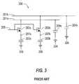
- the CAM cell illustrated in Fig. 2stores a single bit of data, and is therefore capable of encoding only two states.
- ternary CAMsrequire cells which can encode three states.
- the 300 circuit illustrated in Fig. 3is similar to that the circuit 200 illustrated in Fig. 2, but includes two storage elements. This permits the cell 300 to store two bits, which can encode four states, three of which is sufficient to serve the storage requirements of a ternary CAM cell.
- a read operationmay be destructive.
- cell 200for example, when the read operation is performed on a cell in which the capacitor 202 is storing a low level of charge, the flow of charge from the bit line 201 during the read operation alters the charge level of the capacitor 202.
- a charge restoration operationis required after each read operation.
- the requirement for performing a charge restoration operation after each readlimits the speed of a CAM device.
- the charge restoration circuit(not illustrated) also requires additional components and increases power consumption.
- Fig. 4is an illustration of another CAM cell 400.
- CAM cell 400includes two additional transistors 402a, 402b, which are coupled in parallel with the data storage capacitors 203a, 203b, respectively.
- the gate of transistor 402ais coupled to node 207b while the gate of transistor 402b is coupled to node 207a.
- These two transistors 402a, 402bprovide the circuit 400 a limited form of protection from destructive reads. More specifically, the CAM cell 400 can be read nondestructively only if the capacitors 203a, 203b store opposite charges (i.e., "0" + "1" or "1" + “0").
- the CAM cell 400can be used as a dynamic binary CAM cell not requiring charge restoration after a read.
- control circuitrye.g., controller 140 (Fig. 1)
- the CAM cell 400is unsuitable for use as a ternary CAM cell because ternary CAM cells must be able to store at least three states. Accordingly, there is a need and desire for a method and apparatus for an efficient dynamic CAM cell architecture which does not require charge restoration after each read operation.
- JP56029891discloses an associative memory circuit having a self-refresh function.
- the disclosed circuitis limited to the use of MIS transistors, formed into two RAM blocks.
- the present inventionis directed to a ternary CAM cell which stores charge in a manner similar to a DRAM cell, but which also can be non-destructively read. That is, a read operation does not have to be followed by a charge restoration operation in order to maintain data integrity.
- the three required states of a ternary CAM(logical "0", logical "1", and "don't care") may be stored using three bits of storage.
- the use of three bits of storage per CAM cellpermits the use of a circuit topology which include three states which can be read non-destructively.
- a tertiary content addressable memory CAM cellcomprising: a first storage element having a first capacitor controllably coupled via a first switch to a first bit line; a second storage element having a second capacitor controllably coupled via a second switch to a second bit line; a third storage element having a third capacitor controllably coupled via a third switch to a third bit line; wherein said first, second, and third storage elements are coupled to a control circuit which, in response to one of said storage elements being set to a first logical state, sets each of the other storage elements to a second logical state.
- a method for operating a tertiary content addressable memory CAM cellcomprising: setting a first of three binary storage elements to a first binary state to indicate a first tertiary state of said CAM cell, said three binary storage elements each including a capacitor, wherein in response to said first binary storage element being set to a first binary state, said second and third binary storage elements are each set to a second binary state.
- FIG. 1is a block diagram of a content addressable memory.
- FIG. 2is a circuit diagram of a binary CAM cell
- FIG. 3is a circuit diagram of a ternary CAM cell based on the binary CAM cell of FIG. 2;
- FIG. 4is a circuit diagram of a CAM cell having two bits of storage and which may be used as a binary CAM cell which can be read nondestructively;
- FIG. 5is a circuit diagram of tertiary storage element
- FIG. 6is a circuit diagram of a ternary CAM cell having three bits of storage per cell.
- FIG. 7is a block diagram of CAM device using an array of ternary CAM cells as illustrated in FIG. 6.
- FIG. 8is a block diagram of a network device employing a CAM device as illustrated in FIG. 7.
- the CAM cell architecture of the present inventionis illustrated as CAM cell 600 in Fig 6 and utilizes a tertiary storage element having particular properties in order to support reading without requiring a charge restoration operation.
- a tertiary storage elementhaving particular properties in order to support reading without requiring a charge restoration operation.
- the tertiary storage circuit 500(Fig. 5) comprises three NAND gates 501, 502, 503 which couple three inputs D0, D1, D2 to three outputs Q0, Q1, Q2, respectively.
- the output of each NAND gate 501, 502, 503is also coupled as an input to the other NAND gates.
- NAND gate 501has an output Q0 which is provided as an input to NAND gates 502, 503. The use of feedback in this manner limits the number of stable input/output states for the circuit 500.
- the circuit 500supports thee stable states wherein only one of the three inputs D0, D1, D2 of the circuit 500 is at a logical "1" (with the remaining inputs each at a logical "0") and wherein only one of the three outputs Q0, Q1, Q2 is at a logical "0" (with the remaining outputs each at a logical "1").
- These three stables statesarc illustrated in the following truth table. Input Output D0 D1 D2 Q1 Q2 Q3 1 0 0 0 1 1 0 1 0 1 0 1 0 0 1 1 1 0
- One important aspect of the above truth tableis that when one of the outputs (e.g., Q1) is at a logical "0" state, due to the way the NAND gates 501, 502, 503 are coupled, the remaining outputs (e.g., Q2, Q3) are forced to take the logical "1" state.
- one of the outputse.g., Q1
- the remaining outputse.g., Q2, Q3
- the CAM cell 600(Fig. 6) of the present invention is based upon the stable state properties of the above described circuit.
- the CAM cell 600is a dynamic CAM cell and includes three storage elements in the form of capacitors 203a, 203b, 203c. Each capacitor is associated with a respective bit line 201a, 201b, 201c. Access between the bit lines 201a, 201b, 201c and the capacitors 203a, 203b, 203c is governed by transistors 202a, 202b, 202c, each of which has its gate coupled to line 205.
- the capacitors 203a 203b 203care each associated with two discharge devices.
- the discharge devicesare transistors.
- capacitors 203a, 203b, 203care respectively coupled in parallel to a first set of transistors 402a, 402b, and 402c.
- Transistors 402a, 402bhave their gates coupled to node 207c.
- Transistor 402chas its gate coupled to node 207b.
- the capacitors 203a, 203b, 203care also respectively coupled in parallel to transistors 602a, 602b, 602c.
- the gate of transistor 602ais coupled to node 207b.
- Transistors 602b, 602chave their gates coupled together and to node 207a.
- the above described circuit topologyis designed using a principle similar to the tertiary storage circuit 500 (Fig. 5) because the above described circuit topology supports three stable states wherein only one of the three capacitors 203a, 203b, 203c stores a high level of charge (e.g., a logical "1") while the other two capacitors are discharged (e.g., a logical "0").
- the nodes 207a, 207b, 207care respectively associated with capacitors 203a, 203b, 203c and function much like the feedback feature of circuit 500. This is because the charge level of one capacitor is coupled via one of the nodes to control the discharge devices (e.g., 602b, 602c) coupled to the other capacitors.
- node 207awould be at a high potential.
- Node 207ais coupled to the gate of transistor 602b and the gate of transistor 602c, thus both transistors 602b, 602c will be switched on.
- transistor 602bis switched on, charge will flow from capacitor 203b to ground 206 via transistor 602b.
- transistor 602cis turned on, capacitor 203c will discharge to ground 206 via transistor 602c.
- the cell 600can be written by setting one of the bit lines 201a, 201b, 201c to a high logic level (e.g., a logical "1") and the remaining two bit lines 201a, 201b, 201c to a low logical level (e.g., a logical "0").
- a high logic levele.g., a logical "1”
- a low logical levele.g., a logical "0"
- bit lines 201a, 201b, 201chave been set to the appropriate voltage levels, a logical high signal is placed on line 205, causing the gates of transistors 202a, 202b, 202c to conduct, thereby transferring charge corresponding to a high logical level to one of the capacitors 203a, 203b, 203c associated with the bit line 201a, 201b, 201c set to a high logic level and transferring charge corresponding to a low logical level to two of the capacitors 203a, 203b, 203c associated with the bit lines 201a, 201b, 201c set to a low logic level.
- the cell 600can be read by precharging the bit lines 201a, 201b, 201c to high, switching on the access transistors 202a, 202b, 202c, and observing potential changes on the bit lines 201a-201c.
- a capacitorstores a high level of charge, the read process does not reduce the charge level of the capacitors.
- a capacitor at a high logical statewill retain that logical state through a read.
- cell 600when a capacitor is at a low logical state, it will retain that logical state through a read as well because one of the other capacitors will be at a high logical state, ensuring that one of the transistors coupled in parallel to a capacitor having low logical state will discharge to ground.
- the cell 600can therefore be used as a building block for CAM arrays which do not require a charge restoration procedure following each read operation.
- the present inventionis directed to a tertiary CAM cell 600.
- the CAM cell 600(Fig. 6) includes three bits of storage, arranged in a nine transistor architecture.
- the architectureincludes three stables states where only one of the three bits is at a logical "0" while the other two bits are at a logical "1.” These three stable states are sufficient to encode the logical "0", "1", and "don't care” states required in a ternary CAM.
- the three stable statescan also be read without requiring a charge restoration procedure while maintaining the integrity of the storage.
- Fig. 7is an illustration of a CAM device 700 utilizing an array 110' of the CAM cells 600 of the present invention.
- a match detection circuit 120'is coupled to the array 110.
- the CAM device 700may also optionally include a priority encoder 130 coupled to the match detection circuitry 120.
- a control circuit 140'is coupled to the array 110', match detection circuit 120, priority encoder 130, and the data 150a, address 150b, and control 150c signal lines.
- the control circuit 140' and match detection circuit 120'are similar to their conventional counter parts, but have been adapted to work with an encoding which maps the three stable states (i.e., 100, 010, 001) of the CAM cells to the "0", "1", and "don't care" states of a ternary CAM.
- state 100may correspond to a logical "0"
- state 010may correspond to a logical "1”
- state "001"may correspond to a "don't care” state.
- the priority encoder 130may be coupled to the match detection circuit to prioritize the output of the CAM device 700 should multiple entries in the device 700 match a data sample.
- Fig. 8is an illustration of how the CAM device 700 can be used in a network device 800.
- the network device 800might be, for example, a network router 800 which examines each data packet received from input ports 801 and routes each packet to one of a plurality of output ports 805. As data packets are received from each input port 801, they are temporarily stored in an input buffer 802.
- the input buffer 802may be organized as a queue and read by a control logic 803.
- Each packetincludes an address field. Generally, a portion of the address field specifies a network or sub-network address, while another portion of the address field specifies a node on a network/sub-network.
- the control logic 803examines the data packet at the head of the queue 802 and determines which one of the plurality of output ports (each corresponding to, for example, a different network or sub-network) will receive the data packet.
- the control logic 803may also store each newly resolved network/sub-network address-to-output port pairing in the CAM device 700.
- the network or sub-network address from the data packetis extracted and searched by the CAM device 700 for a previously resolved route. In the case of a match, the data packet can be quickly transferred to the correct output port without additional processing.
Landscapes
- Dram (AREA)
- Logic Circuits (AREA)
- Semiconductor Memories (AREA)
Description
- The present invention relates generally to semiconductor memory, and more particularly to a tertiary CAM cell.
- Many applications require searching information at high speed. In many network devices, such as switches or routers, data packets are transferred based on the contents of embedded address information. Thus, in order to achieve a high data transfer rate, network systems must be able to perform very high speed searches and comparisons. One class of circuits useful for this function is a content addressable memory or CAM. It should be noted that although the following discussion is set within the context of a networked system, there are many other applications which require high speed searching and comparison, and which may also therefore benefit from the present invention. For example, the tag field of a fully associative cache memory also requires high speed searching and may be implemented using a CAM.
- It may be useful to compare a CAM against a traditional memory device, such as a random access memory (RAM). To an extent, CAM and RAM device operate conversely. For example, a RAM may be read by presenting it with a read command and an address. The RAM responds by outputting the data stored at the specified address. However, when a CAM is read, it is presented with a data sample, and the CAM returns an match signal indicating whether the data sample is stored in the CAM, and if so, an address within the CAM which contains the data which matched the sample.
- Network routers and switches generally employ a matching function, where a portion of a packet, such as an address field, is compared to a list of data entries. The list is often referred to as a database. Fig. 1 is a block diagram of an
exemplary CAM device 100, which includes aCAM array 110 for storing the database, amatch detection circuit 120 for detecting matches, and optionally apriority encoder 130 for selecting and outputting a matching address in a priority order, when appropriate. The CAM device also includes acontroller 140, for controlling the operation of theCAM array 110,match detection logic 120, andpriority encoder 130, as well as for interfacing theCAM device 100 to other devices via thedata 150a,address 150b, and control 150c lines. Commercially available CAM devices may support, for example, searching a 136-bit wide data sample against a database having up to 16,384 entries. Commercially available CAM devices may be searched at rates up to 100 million searches per second. This ability for CAMs to quickly search relatively wide data words against relatively large databases at high speeds makes them highly useful in applications such as network routing and switching. - There are two types of searches which are of interest, namely a search for the exact match and the partial match search. In the exact match search, an entry stored in the CAM will match the data sample only if the data sample and the entry match bit for bit. In a partial match search, the search may be conducted on only a subset of bits in the word. That is, the CAM entries are permitted to specify a third "don't care" state in addition to the logical "0" and "1" states. When a partial match search is conducted, CAM entries will match a data sample as long as each bit in the entry set at a logical "0" or "1" states match the corresponding portion of the data sample.
- CAMs having entries which only support the logical "0" and logical "1" states are known as binary CAMs, and can only support exact match searches. CAMs having entries which also support the use of the "don't care" state are known as ternary CAMs, and can be used for partial match searches. (These CAMs also support exact match searches when an entry does not contain any "don't care" states.)
- In a ternary CAM, each bit of the database stored in the
CAM array 110 must be represented by at least two bits, in order to encode the three required logical states ("0", "1", and "don't care"). Although a number of different technologies can be used to construct theCAM array 110, modern CAM devices use storage elements based upon a static random access memory (SRAM), where data is stored in a flip-flop, or a dynamic random access memory (DRAM), where data is stored in the form of a charge on a capacitor. Fig. 2 is an illustration of aCAM cell 200 based upon DRAM technology. - The
cell 200 includes atransistor 202 and acapacitor 203, which are coupled in series between abit line 201 and aground potential 206 as illustrated in Fig. 2. Aselect line 205 is coupled to the gate of thetransistor 202. Additionally, thecell 200 inherently includes parasitic capacitance, which is illustrated in Fig. 2 ascapacitor 204, coupled between thebit line 201 andground 206. Data may be stored in thecell 200 by switchingtransistor 202 on (via line 205) and forcingbit line 201 to either a high or a low state. This causes thecapacitor 203 to charge or discharge until the potential atnode 207 equals the potential of the bit line. Thetransistor 202 is then switched off (via line 205) and the potential atnode 207 is maintained by the charge stored incapacitor 203. - In order to read data stored in the
cell 200, thebit line 201 is precharged to a high level. This ensures that theparasitic capacitance 204 is also charged. Thetransistor 202 is then switched on (via line 205). If thecapacitor 203 is storing a charge so that the potential atnode 207 is high, there is no change of potential atnode 207 and at thebit line 201. The charge level of thecapacitor 203 is also unchanged. However, if thecapacitor 203 is storing a charge so that the potential atnode 207 is low, charge will flow from thebit line 201 through thetransistor 202 and into thecapacitor 203. This causes the potential at thebit line 201 to decrease and the potential atnode 207 to increase. The charge level of thecapacitor 203 also increases. The change in voltage in thebit line 201 and/or atnode 207 can be sensed, in order to determine logical stated stored in thecapacitor 202. - The CAM cell illustrated in Fig. 2 stores a single bit of data, and is therefore capable of encoding only two states. As previously discussed, ternary CAMs require cells which can encode three states. The 300 circuit illustrated in Fig. 3 is similar to that the
circuit 200 illustrated in Fig. 2, but includes two storage elements. This permits thecell 300 to store two bits, which can encode four states, three of which is sufficient to serve the storage requirements of a ternary CAM cell. - One problem associated with
dynamic CAM cells cell 200, for example, when the read operation is performed on a cell in which thecapacitor 202 is storing a low level of charge, the flow of charge from thebit line 201 during the read operation alters the charge level of thecapacitor 202. Thus, inCAM cells - Fig. 4 is an illustration of another
CAM cell 400. In comparison to the previously described CAM cell 300 (Fig. 3),CAM cell 400 includes twoadditional transistors data storage capacitors transistor 402a is coupled tonode 207b while the gate oftransistor 402b is coupled tonode 207a. These twotransistors CAM cell 400 can be read nondestructively only if thecapacitors CAM cell 400 were used with control circuitry (e.g., controller 140 (Fig. 1)) which only permits storing inCAM cell 400 the two opposite charge states, theCAM cell 400 can be used as a dynamic binary CAM cell not requiring charge restoration after a read. Unfortunately, theCAM cell 400 is unsuitable for use as a ternary CAM cell because ternary CAM cells must be able to store at least three states. Accordingly, there is a need and desire for a method and apparatus for an efficient dynamic CAM cell architecture which does not require charge restoration after each read operation. - JP56029891 discloses an associative memory circuit having a self-refresh function. The disclosed circuit is limited to the use of MIS transistors, formed into two RAM blocks.
- The present invention is directed to a ternary CAM cell which stores charge in a manner similar to a DRAM cell, but which also can be non-destructively read. That is, a read operation does not have to be followed by a charge restoration operation in order to maintain data integrity. The three required states of a ternary CAM (logical "0", logical "1", and "don't care") may be stored using three bits of storage. The use of three bits of storage per CAM cell permits the use of a circuit topology which include three states which can be read non-destructively.
- In particular, in a first aspect of the invention there is provided a tertiary content addressable memory CAM cell, comprising: a first storage element having a first capacitor controllably coupled via a first switch to a first bit line; a second storage element having a second capacitor controllably coupled via a second switch to a second bit line; a third storage element having a third capacitor controllably coupled via a third switch to a third bit line; wherein said first, second, and third storage elements are coupled to a control circuit which, in response to one of said storage elements being set to a first logical state, sets each of the other storage elements to a second logical state.
- In another aspect of the invention there is provided a method for operating a tertiary content addressable memory CAM cell, comprising: setting a first of three binary storage elements to a first binary state to indicate a first tertiary state of said CAM cell, said three binary storage elements each including a capacitor, wherein in response to said first binary storage element being set to a first binary state, said second and third binary storage elements are each set to a second binary state.
- The foregoing and other advantages and features of the invention will become more apparent from the detailed description of exemplary embodiments of the invention given below with reference to the accompanying drawings in which:
- FIG. 1 is a block diagram of a content addressable memory.
- FIG. 2 is a circuit diagram of a binary CAM cell;
- FIG. 3 is a circuit diagram of a ternary CAM cell based on the binary CAM cell of FIG. 2;
- FIG. 4 is a circuit diagram of a CAM cell having two bits of storage and which may be used as a binary CAM cell which can be read nondestructively;
- FIG. 5 is a circuit diagram of tertiary storage element;
- FIG. 6 is a circuit diagram of a ternary CAM cell having three bits of storage per cell; and
- FIG. 7 is a block diagram of CAM device using an array of ternary CAM cells as illustrated in FIG. 6.
- FIG. 8 is a block diagram of a network device employing a CAM device as illustrated in FIG. 7.
- The CAM cell architecture of the present invention is illustrated as
CAM cell 600 in Fig 6 and utilizes a tertiary storage element having particular properties in order to support reading without requiring a charge restoration operation. However, before discussing in detail the structure and operation of the CAM cell architecture of the present invention, it may be useful to examine the operation of thetertiary storage circuit 500 of Fig. 5, as there are numerous similarities betweencircuit 500 andcell 600. - The tertiary storage circuit 500 (Fig. 5) comprises three
NAND gates NAND gate NAND gate 501 has an output Q0 which is provided as an input toNAND gates circuit 500. In particular, thecircuit 500 supports thee stable states wherein only one of the three inputs D0, D1, D2 of thecircuit 500 is at a logical "1" (with the remaining inputs each at a logical "0") and wherein only one of the three outputs Q0, Q1, Q2 is at a logical "0" (with the remaining outputs each at a logical "1"). These three stables states arc illustrated in the following truth table.Input Output D0 D1 D2 Q1 Q2 Q3 1 0 0 0 1 1 0 1 0 1 0 1 0 0 1 1 1 0 - One important aspect of the above truth table is that when one of the outputs (e.g., Q1) is at a logical "0" state, due to the way the
NAND gates - The CAM cell 600 (Fig. 6) of the present invention is based upon the stable state properties of the above described circuit. The
CAM cell 600 is a dynamic CAM cell and includes three storage elements in the form ofcapacitors respective bit line bit lines capacitors transistors line 205. - The
capacitors 203a203b 203c are each associated with two discharge devices. In one illustrated embodiment, the discharge devices are transistors. For example,capacitors transistors Transistors node 207c.Transistor 402c has its gate coupled tonode 207b. Thecapacitors transistors transistor 602a is coupled tonode 207b.Transistors node 207a. - The above described circuit topology is designed using a principle similar to the tertiary storage circuit 500 (Fig. 5) because the above described circuit topology supports three stable states wherein only one of the three
capacitors nodes capacitors circuit 500. This is because the charge level of one capacitor is coupled via one of the nodes to control the discharge devices (e.g., 602b, 602c) coupled to the other capacitors. For example, ifcapacitor 203a stores a high charge,node 207a would be at a high potential.Node 207a is coupled to the gate oftransistor 602b and the gate oftransistor 602c, thus bothtransistors transistor 602b is switched on, charge will flow fromcapacitor 203b to ground 206 viatransistor 602b. Similarly, whentransistor 602c is turned on,capacitor 203c will discharge toground 206 viatransistor 602c. - The
cell 600 can be written by setting one of thebit lines bit lines bit lines line 205, causing the gates oftransistors capacitors bit line capacitors bit lines - The
cell 600 can be read by precharging thebit lines access transistors bit lines 201a-201c. As previously noted, when a capacitor stores a high level of charge, the read process does not reduce the charge level of the capacitors. Thus, a capacitor at a high logical state will retain that logical state through a read. Incell 600, when a capacitor is at a low logical state, it will retain that logical state through a read as well because one of the other capacitors will be at a high logical state, ensuring that one of the transistors coupled in parallel to a capacitor having low logical state will discharge to ground. Thecell 600 can therefore be used as a building block for CAM arrays which do not require a charge restoration procedure following each read operation. - Thus, the present invention is directed to a
tertiary CAM cell 600. The CAM cell 600 (Fig. 6) includes three bits of storage, arranged in a nine transistor architecture. The architecture includes three stables states where only one of the three bits is at a logical "0" while the other two bits are at a logical "1." These three stable states are sufficient to encode the logical "0", "1", and "don't care" states required in a ternary CAM. The three stable states can also be read without requiring a charge restoration procedure while maintaining the integrity of the storage. - Fig. 7 is an illustration of a
CAM device 700 utilizing an array 110' of theCAM cells 600 of the present invention. A match detection circuit 120' is coupled to thearray 110. TheCAM device 700 may also optionally include apriority encoder 130 coupled to thematch detection circuitry 120. A control circuit 140' is coupled to the array 110',match detection circuit 120,priority encoder 130, and thedata 150a,address 150b, and control 150c signal lines. The control circuit 140' and match detection circuit 120' are similar to their conventional counter parts, but have been adapted to work with an encoding which maps the three stable states (i.e., 100, 010, 001) of the CAM cells to the "0", "1", and "don't care" states of a ternary CAM. For example,state 100 may correspond to a logical "0", whilestate 010 may correspond to a logical "1", and state "001" may correspond to a "don't care" state. Thepriority encoder 130 may be coupled to the match detection circuit to prioritize the output of theCAM device 700 should multiple entries in thedevice 700 match a data sample. - Fig. 8 is an illustration of how the
CAM device 700 can be used in anetwork device 800. Thenetwork device 800 might be, for example, anetwork router 800 which examines each data packet received frominput ports 801 and routes each packet to one of a plurality ofoutput ports 805. As data packets are received from eachinput port 801, they are temporarily stored in aninput buffer 802. Theinput buffer 802 may be organized as a queue and read by acontrol logic 803. Each packet includes an address field. Generally, a portion of the address field specifies a network or sub-network address, while another portion of the address field specifies a node on a network/sub-network. Thecontrol logic 803 examines the data packet at the head of thequeue 802 and determines which one of the plurality of output ports (each corresponding to, for example, a different network or sub-network) will receive the data packet. Thecontrol logic 803 may also store each newly resolved network/sub-network address-to-output port pairing in theCAM device 700. When a new packet is examined by the control logic 703, the network or sub-network address from the data packet is extracted and searched by theCAM device 700 for a previously resolved route. In the case of a match, the data packet can be quickly transferred to the correct output port without additional processing.
Claims (11)
- A tertiary content addressable memory, CAM, cell (600), comprising:a first storage element having a first capacitor (203a) controllably coupled via a first switch (202a) to a first bit line (201a);a second storage element having a second capacitor (203b) controllably coupled via a second switch (202b) to a second bit line (201b);a third storage element having a third capacitor (203c) controllably coupled via a third switch (202c) to a third bit line (201c);wherein said first, second, and third storage elements are coupled to a control circuit which, in response to one of said storage elements being set to a first logical state, sets each of the other storage elements to a second logical state.
- The tertiary CAM cell of claim 1, wherein said first, second, and third switches (202a, 202b, 202c) are transistors.
- The tertiary CAM cell of claim 1, wherein said control circuit further comprises:a first pair (402a, 602a) of controllable discharge devices, coupled in parallel between a ground potential (206) and the first capacitor (203a);a second pair (402b, 602b) of controllable discharge devices, coupled in parallel between the ground potential (206) and the second capacitor (203b); anda third pair (402c, 602c) of controllable discharge devices, coupled in parallel between the ground potential (206) and the third capacitor (203c);wherein said first pair (402a, 602a) of controllable discharge devices are arranged to set first capacitor (203a) to correspond to the second logical state if either the second or third capacitors (203b, 203c) are set to store a charge associated with the first logical state;
wherein said second pair (402b, 602b) of controllable discharge devices are arranged to set said second capacitor (203b) to correspond to the second logical state if either the first or third capacitors (203a, 203c) are set to store a charge associated with the first logical state; and
wherein said third pair (402c, 602c) of controllable discharge devices are arranged to set said third capacitor (203c) to correspond to the second logical state if either the first or second capacitors (203a, 203b) are set to store a charge associated with the first logical state. - The CAM cell of claim 3, wherein said controllable discharge devices are transistors having a first source/drain terminal coupled to a first terminal of one of said capacitors (203a, 203b, 203c) and a second source/drain terminal coupled to the ground potential (206).
- A method for operating a tertiary content addressable memory, CAM, cell (600), comprising:setting a first of three binary storage elements to a first binary state to indicate a first tertiary state of said CAM cell (600), said three binary storage elements each including a capacitor (203a, 203b, 203c),wherein in response to said first binary storage element being set to a first binary state, said second and third binary storage elements are each set to a second binary state.
- The method of claim 5, further comprising:setting the second of three binary storage elements to a first binary state to indicate a second tertiary state of said CAM cell (600),wherein in response to said second binary storage element being set to a first binary state, said first and third binary storage elements are each set to a second binary state.
- The method of claim 6, further comprising:setting the third of three binary storage elements to a first binary state to indicate a third tertiary state of said CAM cell (600),wherein in response to said third binary storage element being set to a first binary state, said first and second binary storage elements are each set to a second binary state.
- The method of claim 7, wherein said first, second, and third tertiary states are members of a set consisting of the following elements:a binary "0";a binary "1"; anda "don't care" state.
- The method of claim 5, further comprising reading the state of said first binary storage element, said reading further comprising the steps of:precharging a first bit line (201a) controllably coupled to said first storage element to a predetermined level;coupling said first bit line (201 a) to said first binary storage element; andsensing a change in potential of said first bit line;wherein said reading does not change the state of said first storage element.
- The method of claim 6, further comprising reading the state of said second binary storage element, said reading further comprising the steps of:precharging a second bit line (201b) controllably coupled to said second storage element to a predetermined level;coupling said second bit line (201b) to said second binary storage element; andsensing a change in potential of said second bit line;wherein said reading does not change the state of said second storage element.
- The method of claim 7, further comprising reading the state of said third binary storage element, said reading further comprising the steps of:precharging a third bit line (201c) controllably coupled to said third storage element to a predetermined level;coupling said third bit line (201c) to said third binary storage element; andsensing a change in potential of said third bit line;wherein said reading does not change the state of said third storage element.
Applications Claiming Priority (5)
| Application Number | Priority Date | Filing Date | Title |
|---|---|---|---|
| US32446201P | 2001-09-25 | 2001-09-25 | |
| US324462P | 2001-09-25 | ||
| US10/202,003US6781856B2 (en) | 2001-09-25 | 2002-07-25 | Tertiary CAM cell |
| US202003 | 2002-07-25 | ||
| PCT/US2002/029749WO2003028034A2 (en) | 2001-09-25 | 2002-09-23 | A tertiary cam cell |
Publications (2)
| Publication Number | Publication Date |
|---|---|
| EP1433180A2 EP1433180A2 (en) | 2004-06-30 |
| EP1433180B1true EP1433180B1 (en) | 2007-01-10 |
Family
ID=26897277
Family Applications (1)
| Application Number | Title | Priority Date | Filing Date |
|---|---|---|---|
| EP02770532AExpired - LifetimeEP1433180B1 (en) | 2001-09-25 | 2002-09-23 | A tertiary cam cell |
Country Status (8)
| Country | Link |
|---|---|
| US (2) | US6781856B2 (en) |
| EP (1) | EP1433180B1 (en) |
| JP (2) | JP3981665B2 (en) |
| KR (1) | KR100565456B1 (en) |
| CN (1) | CN100440379C (en) |
| AU (1) | AU2002335768A1 (en) |
| DE (1) | DE60217526T2 (en) |
| WO (1) | WO2003028034A2 (en) |
Families Citing this family (10)
| Publication number | Priority date | Publication date | Assignee | Title |
|---|---|---|---|---|
| US6751110B2 (en)* | 2002-03-08 | 2004-06-15 | Micron Technology, Inc. | Static content addressable memory cell |
| US20060203529A1 (en)* | 2003-09-05 | 2006-09-14 | William Radke | Cutting CAM peak power by clock regioning |
| US8169808B2 (en) | 2008-01-25 | 2012-05-01 | Micron Technology, Inc. | NAND flash content addressable memory |
| US8238173B2 (en)* | 2009-07-16 | 2012-08-07 | Zikbit Ltd | Using storage cells to perform computation |
| US9076527B2 (en) | 2009-07-16 | 2015-07-07 | Mikamonu Group Ltd. | Charge sharing in a TCAM array |
| US8732560B2 (en)* | 2012-05-08 | 2014-05-20 | Infineon Technologies Ag | Method and device for correction of ternary stored binary data |
| US8935590B2 (en)* | 2012-10-31 | 2015-01-13 | Infineon Technologies Ag | Circuitry and method for multi-bit correction |
| US9792988B2 (en) | 2014-08-12 | 2017-10-17 | Ciena Corporation | Parallel turbine ternary content addressable memory for high-speed applications |
| DE102017110208B4 (en)* | 2017-05-11 | 2019-03-07 | Universität Rostock | Signal processing device and measuring device for high-precision transit time measurement of at least three signals |
| CN110830169A (en)* | 2019-11-12 | 2020-02-21 | 深圳市本特利科技有限公司 | Ternary coding method for electronic detonator detection device |
Family Cites Families (12)
| Publication number | Priority date | Publication date | Assignee | Title |
|---|---|---|---|---|
| JPS6045502B2 (en) | 1979-08-13 | 1985-10-09 | 日本電信電話株式会社 | Semiconductor content addressable memory circuit |
| US4622653A (en) | 1984-10-29 | 1986-11-11 | Texas Instruments Incorporated | Block associative memory |
| KR0135699B1 (en) | 1994-07-11 | 1998-04-24 | 김주용 | Self-Refreshing Dual-Port Dynamic Cam Cells and Refreshers |
| US5642322A (en) | 1995-05-24 | 1997-06-24 | Kawasaki Steel Corporation | Layout of semiconductor memory and content-addressable memory |
| JP3190868B2 (en)* | 1997-11-21 | 2001-07-23 | エヌイーシーマイクロシステム株式会社 | Associative memory device |
| US6081440A (en)* | 1998-11-05 | 2000-06-27 | Lara Technology, Inc. | Ternary content addressable memory (CAM) having fast insertion and deletion of data values |
| US6266262B1 (en)* | 1998-11-05 | 2001-07-24 | Lara Technology, Inc. | Enhanced binary content addressable memory for longest prefix address matching |
| US5999435A (en) | 1999-01-15 | 1999-12-07 | Fast-Chip, Inc. | Content addressable memory device |
| US6542391B2 (en)* | 2000-06-08 | 2003-04-01 | Netlogic Microsystems, Inc. | Content addressable memory with configurable class-based storage partition |
| US6647457B1 (en)* | 1999-11-16 | 2003-11-11 | Cypress Semiconductor Corporation | Content addressable memory having prioritization of unoccupied entries |
| US6331961B1 (en) | 2000-06-09 | 2001-12-18 | Silicon Access Networks, Inc. | DRAM based refresh-free ternary CAM |
| EP1271548B1 (en)* | 2001-06-22 | 2008-05-14 | STMicroelectronics Limited | Associative memory with AND gate match signal combining circuitry |
- 2002
- 2002-07-25USUS10/202,003patent/US6781856B2/ennot_activeExpired - Fee Related
- 2002-09-23JPJP2003531472Apatent/JP3981665B2/ennot_activeExpired - Fee Related
- 2002-09-23WOPCT/US2002/029749patent/WO2003028034A2/enactiveIP Right Grant
- 2002-09-23DEDE60217526Tpatent/DE60217526T2/ennot_activeExpired - Lifetime
- 2002-09-23EPEP02770532Apatent/EP1433180B1/ennot_activeExpired - Lifetime
- 2002-09-23CNCNB028233271Apatent/CN100440379C/ennot_activeExpired - Fee Related
- 2002-09-23KRKR1020047004292Apatent/KR100565456B1/ennot_activeExpired - Fee Related
- 2002-09-23AUAU2002335768Apatent/AU2002335768A1/ennot_activeAbandoned
- 2003
- 2003-10-15USUS10/684,388patent/US6785153B2/ennot_activeExpired - Fee Related
- 2007
- 2007-04-26JPJP2007117545Apatent/JP2007265604A/enactivePending
Also Published As
| Publication number | Publication date |
|---|---|
| US20040081000A1 (en) | 2004-04-29 |
| KR20040037108A (en) | 2004-05-04 |
| US20030063485A1 (en) | 2003-04-03 |
| DE60217526D1 (en) | 2007-02-22 |
| CN1592935A (en) | 2005-03-09 |
| JP2005505089A (en) | 2005-02-17 |
| CN100440379C (en) | 2008-12-03 |
| US6785153B2 (en) | 2004-08-31 |
| JP2007265604A (en) | 2007-10-11 |
| JP3981665B2 (en) | 2007-09-26 |
| WO2003028034A3 (en) | 2003-10-30 |
| WO2003028034A2 (en) | 2003-04-03 |
| AU2002335768A1 (en) | 2003-04-07 |
| EP1433180A2 (en) | 2004-06-30 |
| DE60217526T2 (en) | 2007-11-08 |
| US6781856B2 (en) | 2004-08-24 |
| KR100565456B1 (en) | 2006-03-30 |
Similar Documents
| Publication | Publication Date | Title |
|---|---|---|
| US7269040B2 (en) | Static content addressable memory cell | |
| US7433217B1 (en) | Content addressable memory cell configurable between multiple modes and method therefor | |
| US5949696A (en) | Differential dynamic content addressable memory and high speed network address filtering | |
| US6108227A (en) | Content addressable memory having binary and ternary modes of operation | |
| US6310880B1 (en) | Content addressable memory cells and systems and devices using the same | |
| US6781857B1 (en) | Content addressable memory (CAM) devices that utilize multi-port CAM cells and control logic to support multiple overlapping search cycles that are asynchronously timed relative to each other | |
| US20030179623A1 (en) | CAM cell array, TCAM cell, TCAM cell array, address search memory, and network address search apparatus | |
| JP2007265604A (en) | Ternary cam cell | |
| US20050213359A1 (en) | Hybrid content addressable memory | |
| US20030005210A1 (en) | Intelligent CAM cell for CIDR processor | |
| JP2000353388A (en) | Improvement of memory that can refer to contents | |
| US20040228155A1 (en) | Folded dram cam cell | |
| US11631459B2 (en) | Dual compare ternary content addressable memory | |
| US6898100B2 (en) | Semiconductor memory device used for cache memory | |
| US6751112B2 (en) | Dense content addressable memory cell | |
| US7099171B2 (en) | Content addressable memory cell techniques | |
| KR101136578B1 (en) | Ternary content addressable memory | |
| EP0805457A2 (en) | Contents addressable memories | |
| GB2312769A (en) | Contents addressable memory | |
| EP1357558A1 (en) | Dense content addressable memory cell |
Legal Events
| Date | Code | Title | Description |
|---|---|---|---|
| PUAI | Public reference made under article 153(3) epc to a published international application that has entered the european phase | Free format text:ORIGINAL CODE: 0009012 | |
| 17P | Request for examination filed | Effective date:20040421 | |
| AK | Designated contracting states | Kind code of ref document:A2 Designated state(s):AT BE BG CH CY CZ DE DK EE ES FI FR GB GR IE IT LI LU MC NL PT SE SK TR | |
| AX | Request for extension of the european patent | Extension state:AL LT LV MK RO SI | |
| GRAP | Despatch of communication of intention to grant a patent | Free format text:ORIGINAL CODE: EPIDOSNIGR1 | |
| GRAS | Grant fee paid | Free format text:ORIGINAL CODE: EPIDOSNIGR3 | |
| GRAA | (expected) grant | Free format text:ORIGINAL CODE: 0009210 | |
| AK | Designated contracting states | Kind code of ref document:B1 Designated state(s):AT BE BG CH CY CZ DE DK EE ES FI FR GB GR IE IT LI LU MC NL PT SE SK TR | |
| PG25 | Lapsed in a contracting state [announced via postgrant information from national office to epo] | Ref country code:LI Free format text:LAPSE BECAUSE OF FAILURE TO SUBMIT A TRANSLATION OF THE DESCRIPTION OR TO PAY THE FEE WITHIN THE PRESCRIBED TIME-LIMIT Effective date:20070110 Ref country code:NL Free format text:LAPSE BECAUSE OF FAILURE TO SUBMIT A TRANSLATION OF THE DESCRIPTION OR TO PAY THE FEE WITHIN THE PRESCRIBED TIME-LIMIT Effective date:20070110 Ref country code:CH Free format text:LAPSE BECAUSE OF FAILURE TO SUBMIT A TRANSLATION OF THE DESCRIPTION OR TO PAY THE FEE WITHIN THE PRESCRIBED TIME-LIMIT Effective date:20070110 Ref country code:DK Free format text:LAPSE BECAUSE OF FAILURE TO SUBMIT A TRANSLATION OF THE DESCRIPTION OR TO PAY THE FEE WITHIN THE PRESCRIBED TIME-LIMIT Effective date:20070110 Ref country code:FI Free format text:LAPSE BECAUSE OF FAILURE TO SUBMIT A TRANSLATION OF THE DESCRIPTION OR TO PAY THE FEE WITHIN THE PRESCRIBED TIME-LIMIT Effective date:20070110 Ref country code:AT Free format text:LAPSE BECAUSE OF FAILURE TO SUBMIT A TRANSLATION OF THE DESCRIPTION OR TO PAY THE FEE WITHIN THE PRESCRIBED TIME-LIMIT Effective date:20070110 | |
| REG | Reference to a national code | Ref country code:GB Ref legal event code:FG4D | |
| REG | Reference to a national code | Ref country code:IE Ref legal event code:FG4D | |
| REF | Corresponds to: | Ref document number:60217526 Country of ref document:DE Date of ref document:20070222 Kind code of ref document:P | |
| PG25 | Lapsed in a contracting state [announced via postgrant information from national office to epo] | Ref country code:SE Free format text:LAPSE BECAUSE OF FAILURE TO SUBMIT A TRANSLATION OF THE DESCRIPTION OR TO PAY THE FEE WITHIN THE PRESCRIBED TIME-LIMIT Effective date:20070410 | |
| PG25 | Lapsed in a contracting state [announced via postgrant information from national office to epo] | Ref country code:BG Free format text:LAPSE BECAUSE OF THE APPLICANT RENOUNCES Effective date:20070411 | |
| PG25 | Lapsed in a contracting state [announced via postgrant information from national office to epo] | Ref country code:ES Free format text:LAPSE BECAUSE OF FAILURE TO SUBMIT A TRANSLATION OF THE DESCRIPTION OR TO PAY THE FEE WITHIN THE PRESCRIBED TIME-LIMIT Effective date:20070421 | |
| ET | Fr: translation filed | ||
| PG25 | Lapsed in a contracting state [announced via postgrant information from national office to epo] | Ref country code:PT Free format text:LAPSE BECAUSE OF FAILURE TO SUBMIT A TRANSLATION OF THE DESCRIPTION OR TO PAY THE FEE WITHIN THE PRESCRIBED TIME-LIMIT Effective date:20070611 | |
| NLV1 | Nl: lapsed or annulled due to failure to fulfill the requirements of art. 29p and 29m of the patents act | ||
| REG | Reference to a national code | Ref country code:CH Ref legal event code:PL | |
| PLBE | No opposition filed within time limit | Free format text:ORIGINAL CODE: 0009261 | |
| STAA | Information on the status of an ep patent application or granted ep patent | Free format text:STATUS: NO OPPOSITION FILED WITHIN TIME LIMIT | |
| PG25 | Lapsed in a contracting state [announced via postgrant information from national office to epo] | Ref country code:SK Free format text:LAPSE BECAUSE OF FAILURE TO SUBMIT A TRANSLATION OF THE DESCRIPTION OR TO PAY THE FEE WITHIN THE PRESCRIBED TIME-LIMIT Effective date:20070110 | |
| 26N | No opposition filed | Effective date:20071011 | |
| PG25 | Lapsed in a contracting state [announced via postgrant information from national office to epo] | Ref country code:BE Free format text:LAPSE BECAUSE OF FAILURE TO SUBMIT A TRANSLATION OF THE DESCRIPTION OR TO PAY THE FEE WITHIN THE PRESCRIBED TIME-LIMIT Effective date:20070110 Ref country code:CZ Free format text:LAPSE BECAUSE OF FAILURE TO SUBMIT A TRANSLATION OF THE DESCRIPTION OR TO PAY THE FEE WITHIN THE PRESCRIBED TIME-LIMIT Effective date:20070110 | |
| PG25 | Lapsed in a contracting state [announced via postgrant information from national office to epo] | Ref country code:MC Free format text:LAPSE BECAUSE OF NON-PAYMENT OF DUE FEES Effective date:20070930 Ref country code:GR Free format text:LAPSE BECAUSE OF FAILURE TO SUBMIT A TRANSLATION OF THE DESCRIPTION OR TO PAY THE FEE WITHIN THE PRESCRIBED TIME-LIMIT Effective date:20070411 | |
| PG25 | Lapsed in a contracting state [announced via postgrant information from national office to epo] | Ref country code:IE Free format text:LAPSE BECAUSE OF NON-PAYMENT OF DUE FEES Effective date:20070924 | |
| PG25 | Lapsed in a contracting state [announced via postgrant information from national office to epo] | Ref country code:EE Free format text:LAPSE BECAUSE OF FAILURE TO SUBMIT A TRANSLATION OF THE DESCRIPTION OR TO PAY THE FEE WITHIN THE PRESCRIBED TIME-LIMIT Effective date:20070110 | |
| PG25 | Lapsed in a contracting state [announced via postgrant information from national office to epo] | Ref country code:CY Free format text:LAPSE BECAUSE OF FAILURE TO SUBMIT A TRANSLATION OF THE DESCRIPTION OR TO PAY THE FEE WITHIN THE PRESCRIBED TIME-LIMIT Effective date:20070110 | |
| PG25 | Lapsed in a contracting state [announced via postgrant information from national office to epo] | Ref country code:LU Free format text:LAPSE BECAUSE OF NON-PAYMENT OF DUE FEES Effective date:20070923 | |
| PG25 | Lapsed in a contracting state [announced via postgrant information from national office to epo] | Ref country code:TR Free format text:LAPSE BECAUSE OF FAILURE TO SUBMIT A TRANSLATION OF THE DESCRIPTION OR TO PAY THE FEE WITHIN THE PRESCRIBED TIME-LIMIT Effective date:20070110 | |
| PGFP | Annual fee paid to national office [announced via postgrant information from national office to epo] | Ref country code:FR Payment date:20100921 Year of fee payment:9 Ref country code:IT Payment date:20100922 Year of fee payment:9 | |
| PGFP | Annual fee paid to national office [announced via postgrant information from national office to epo] | Ref country code:GB Payment date:20100922 Year of fee payment:9 | |
| PGFP | Annual fee paid to national office [announced via postgrant information from national office to epo] | Ref country code:DE Payment date:20100915 Year of fee payment:9 | |
| GBPC | Gb: european patent ceased through non-payment of renewal fee | Effective date:20110923 | |
| PG25 | Lapsed in a contracting state [announced via postgrant information from national office to epo] | Ref country code:IT Free format text:LAPSE BECAUSE OF NON-PAYMENT OF DUE FEES Effective date:20110923 | |
| REG | Reference to a national code | Ref country code:FR Ref legal event code:ST Effective date:20120531 | |
| REG | Reference to a national code | Ref country code:DE Ref legal event code:R119 Ref document number:60217526 Country of ref document:DE Effective date:20120403 | |
| PG25 | Lapsed in a contracting state [announced via postgrant information from national office to epo] | Ref country code:DE Free format text:LAPSE BECAUSE OF NON-PAYMENT OF DUE FEES Effective date:20120403 | |
| PG25 | Lapsed in a contracting state [announced via postgrant information from national office to epo] | Ref country code:GB Free format text:LAPSE BECAUSE OF NON-PAYMENT OF DUE FEES Effective date:20110923 Ref country code:FR Free format text:LAPSE BECAUSE OF NON-PAYMENT OF DUE FEES Effective date:20110930 |